Embed Size (px)
Citation preview
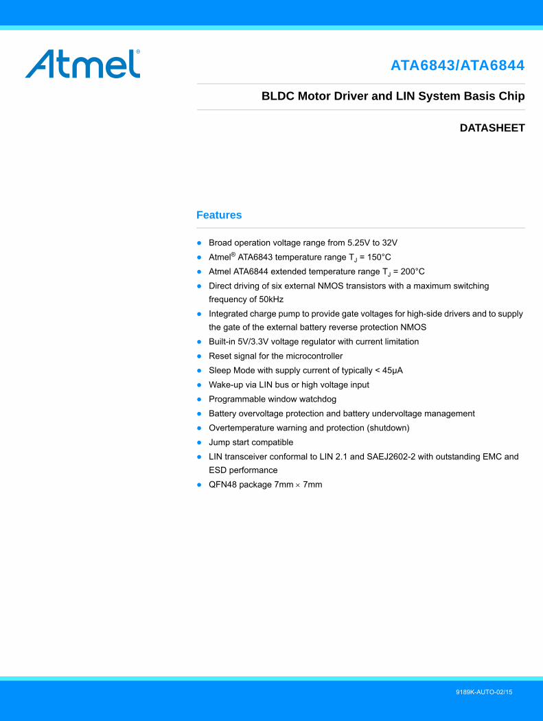
ATA6843/ATA6844
BLDC Motor Driver and LIN System Basis Chip
DATASHEET
Features
● Broad operation voltage range from 5.25V to 32V
● Atmel® ATA6843 temperature range TJ = 150°C
● Atmel ATA6844 extended temperature range TJ = 200°C
● Direct driving of six external NMOS transistors with a maximum switching
frequency of 50kHz
● Integrated charge pump to provide gate voltages for high-side drivers and to supply
the gate of the external battery reverse protection NMOS
● Built-in 5V/3.3V voltage regulator with current limitation
● Reset signal for the microcontroller
● Sleep Mode with supply current of typically < 45µA
● Wake-up via LIN bus or high voltage input
● Programmable window watchdog
● Battery overvoltage protection and battery undervoltage management
● Overtemperature warning and protection (shutdown)
● Jump start compatible
● LIN transceiver conformal to LIN 2.1 and SAEJ2602-2 with outstanding EMC and
ESD performance
● QFN48 package 7mm 7mm
9189K-AUTO-02/15
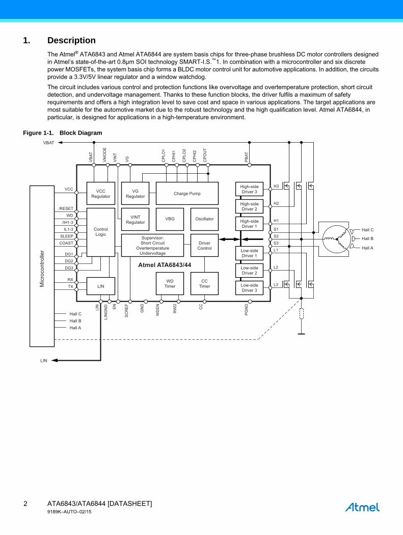
1. Description
The Atmel® ATA6843 and Atmel ATA6844 are system basis chips for three-phase brushless DC motor controllers designed in Atmel’s state-of-the-art 0.8µm SOI technology SMART-I.S.™1. In combination with a microcontroller and six discrete power MOSFETs, the system basis chip forms a BLDC motor control unit for automotive applications. In addition, the circuits provide a 3.3V/5V linear regulator and a window watchdog.
The circuit includes various control and protection functions like overvoltage and overtemperature protection, short circuit detection, and undervoltage management. Thanks to these function blocks, the driver fulfils a maximum of safety requirements and offers a high integration level to save cost and space in various applications. The target applications are most suitable for the automotive market due to the robust technology and the high qualification level. Atmel ATA6844, in particular, is designed for applications in a high-temperature environment.
Figure 1-1. Block Diagram
Supervisor:Short Circuit
OvertemperatureUndervoltage
Charge Pump
CCTimer
WDTimer
VBG
LIN
LIN
Hall CHall BHall A
Hall C
Hall B
Hall A
Atmel ATA6843/44
Oscillator
DriverControl
VINTRegulator
ControlLogic
VGRegulator
LIN
VBAT
Mic
roco
ntro
ller
VIN
T
CPH
I1
CPH
I2
CPL
O1
PBAT
CPO
UT
CPL
O2
VGVMO
DE
High-sideDriver 1
High-sideDriver 2
High-sideDriver 3VCC
Regulator
Low-sideDriver 3
Low-sideDriver 2
Low-sideDriver 1
L2
L1
L3
H2
H3
VBAT
DG3
/RESET
DG2
DG1
WD
/IH1-3
SLEEP
COAST
IL1-3
TX
RX
VCC
H1
S2
S3
S1
LIN
GN
D
WD
EN
GN
D
PGN
D
RW
D
CC
SCR
EFEN
ATA6843/ATA6844 [DATASHEET]9189K–AUTO–02/15
2
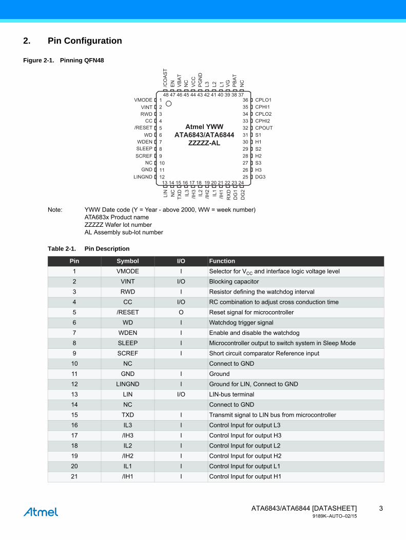
2. Pin Configuration
Figure 2-1. Pinning QFN48
Note: YWW Date code (Y = Year - above 2000, WW = week number)ATA683x Product nameZZZZZ Wafer lot numberAL Assembly sub-lot number
RWD
WDENSLEEPSCREF
LINGNDGND
NC
CC
WD/RESET
VMODEVINT
Atmel YWWATA6843/ATA6844
ZZZZZ-AL
CPLO1CPHI1CPLO2CPHI2CPOUTS1H1S2H2S3H3DG3
NC
PBAT
VGL1L2L3PGN
D
VBAT
EN/CO
AST
NC
VCC
TXD
/IH3
IL2
/IH2
RXD DG
1D
G2
/IH1
IL1
IL3
NC
LIN
48 47 46 45 44 43 42 41 40 39 38 37
13 14 15 16 17 18 19 20 21 22 23 24
123456789101112
363534333231302928272625
Table 2-1. Pin Description
Pin Symbol I/O Function
1 VMODE I Selector for VCC and interface logic voltage level
2 VINT I/O Blocking capacitor
3 RWD I Resistor defining the watchdog interval
4 CC I/O RC combination to adjust cross conduction time
5 /RESET O Reset signal for microcontroller
6 WD I Watchdog trigger signal
7 WDEN I Enable and disable the watchdog
8 SLEEP I Microcontroller output to switch system in Sleep Mode
9 SCREF I Short circuit comparator Reference input
10 NC Connect to GND
11 GND I Ground
12 LINGND I Ground for LIN, Connect to GND
13 LIN I/O LIN-bus terminal
14 NC Connect to GND
15 TXD I Transmit signal to LIN bus from microcontroller
16 IL3 I Control Input for output L3
17 /IH3 I Control Input for output H3
18 IL2 I Control Input for output L2
19 /IH2 I Control Input for output H2
20 IL1 I Control Input for output L1
21 /IH1 I Control Input for output H1
3ATA6843/ATA6844 [DATASHEET]9189K–AUTO–02/15
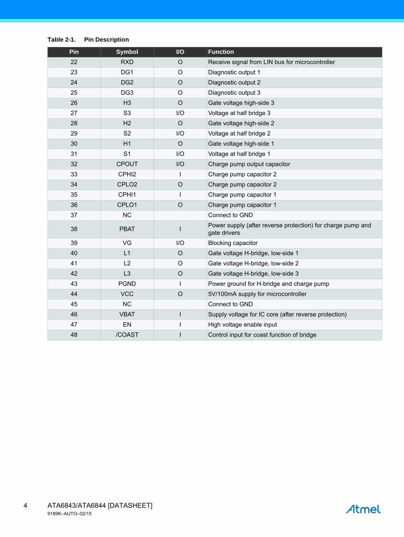
22 RXD O Receive signal from LIN bus for microcontroller
23 DG1 O Diagnostic output 1
24 DG2 O Diagnostic output 2
25 DG3 O Diagnostic output 3
26 H3 O Gate voltage high-side 3
27 S3 I/O Voltage at half bridge 3
28 H2 O Gate voltage high-side 2
29 S2 I/O Voltage at half bridge 2
30 H1 O Gate voltage high-side 1
31 S1 I/O Voltage at half bridge 1
32 CPOUT I/O Charge pump output capacitor
33 CPHI2 I Charge pump capacitor 2
34 CPLO2 O Charge pump capacitor 2
35 CPHI1 I Charge pump capacitor 1
36 CPLO1 O Charge pump capacitor 1
37 NC Connect to GND
38 PBAT IPower supply (after reverse protection) for charge pump and gate drivers
39 VG I/O Blocking capacitor
40 L1 O Gate voltage H-bridge, low-side 1
41 L2 O Gate voltage H-bridge, low-side 2
42 L3 O Gate voltage H-bridge, low-side 3
43 PGND I Power ground for H-bridge and charge pump
44 VCC O 5V/100mA supply for microcontroller
45 NC Connect to GND
46 VBAT I Supply voltage for IC core (after reverse protection)
47 EN I High voltage enable input
48 /COAST I Control input for coast function of bridge
Table 2-1. Pin Description
Pin Symbol I/O Function
ATA6843/ATA6844 [DATASHEET]9189K–AUTO–02/15
4
3. Functional Description
3.1 Power Supply Unit with Supervisor Functions
3.1.1 Power Supply
The IC has to be supplied by a reverse-protected battery voltage. To prevent damage to the IC, proper external protection circuitry has to be added. It is recommended to use at least one capacitor combination of storage and RF capacitors be-hind the reverse protection circuitry, which is connected close to the VBAT and GND pins of the IC.
A fully integrated low-power and low-drop regulator (VINT regulator), stabilized by an external blocking capacitor, provides the necessary low-voltage supply needed for the wake-up process. A trimmed low-power band gap is used as reference for the VINT regulator as well as for the VCC regulator. All internal blocks are supplied by VINT regulator. VINT regulator must not be used for any external supply purposes.
Nothing inside the IC except the logic interface to the external microcontroller is supplied by the 5V/3.3V VCC regulator.
Both voltage regulators are checked by a “power-good comparator”, which keeps the whole chip in reset as long as the internal supply voltage (VINT regulator output) is too low and gnerates a reset for the external microcontroller if the out-put voltage of the VCC regulator is not sufficient.
3.1.2 Voltage Supervisor
This function is implemented to protect the IC and the external power MOS transistors from damage due to overvoltage on PBAT input. In the event of overvoltage (VTHOV) or undervoltage (VTHUV), the external NMOS motor driver transistors will be switched off. The failure state will be flagged on DG2 pin. It is recommended to block PBAT with an external RF capacitor to suppress high frequency disturbances.
3.1.3 Temperature Supervisor
An integrated temperature sensor prevents the IC from overheating. If the temperature is above the overtemperature prewarning threshold TJPW set, the diagnostic pin DG3 will be switched to HIGH to signal this event to the external microcontroller. The microcontroller should take actions to reduce the power dissipation in the IC. If the temperature rises above the overtemperature shutdown threshold TJ switch off, the VCC regulator and all output drivers together with the LIN transceiver will be switched OFF immediately and the /RESET signal will go LOW. Both thresholds have a built-in hysteresis to avoid oscillations. The IC will return to normal operation (Active Mode) when it has cooled down below the shutdown threshold. When the junction temperature drops below the pre-warning threshold, bit DG3 will be switched LOW.
5ATA6843/ATA6844 [DATASHEET]9189K–AUTO–02/15
3.2 Active Mode and Sleep Mode
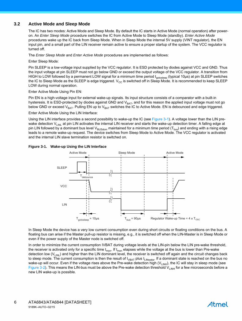
The IC has two modes: Active Mode and Sleep Mode. By default the IC starts in Active Mode (normal operation) after power-on. An Enter Sleep Mode procedure switches the IC from Active Mode to Sleep Mode (standby). Enter Active Mode procedures wake up the IC back from Sleep Mode. When in Sleep Mode the internal 5V supply (VINT regulator), the EN input pin, and a small part of the LIN receiver remain active to ensure a proper startup of the system. The VCC regulator is turned off.
The Enter Sleep Mode and Enter Active Mode procedures are implemented as follows:
Enter Sleep Mode:
Pin SLEEP is a low-voltage input supplied by the VCC regulator. It is ESD protected by diodes against VCC and GND. Thus the input voltage at pin SLEEP must not go below GND or exceed the output voltage of the VCC regulator. A transition from HIGH to LOW followed by a permanent LOW signal for a minimum time period tgotosleep (typical 10µs) at pin SLEEP switches the IC to Sleep Mode as the SLEEP is edge triggered. VCC is switched off in Sleep Mode. It is recommended to keep SLEEP LOW during normal operation.
Enter Active Mode Using Pin EN:
Pin EN is a high-voltage input for external wake-up signals. Its input structure consists of a comparator with a built-in hysteresis. It is ESD-protected by diodes against GND and VBAT, and for this reason the applied input voltage must not go below GND or exceed VBAT. Pulling EN up to VBAT switches the IC to Active Mode. EN is debounced and edge triggered.
Enter Active Mode Using the LIN Interface:
Using the LIN interface provides a second possibility to wake-up the IC (see Figure 3-1). A voltage lower than the LIN pre-wake detection VLINL at pin LIN activates the internal LIN receiver and starts the wake-up detection timer. A falling edge at pin LIN followed by a dominant bus level VBUSdom maintained for a minimum time period (Tbus) and ending with a rising edge leads to a remote wake-up request. The device switches from Sleep Mode to Active Mode. The VCC regulator is activated and the internal LIN slave termination resistor is switched on.
Figure 3-1. Wake-up Using the LIN Interface
In Sleep Mode the device has a very low current consumption even during short circuits or floating conditions on the bus. A floating bus can arise if the Master pull-up resistor is missing, e.g., it is switched off when the LIN-Master is in Sleep Mode or even if the power supply of the Master node is switched off.
In order to minimize the current consumption IVBAT during voltage levels at the LIN-pin below the LIN pre-wake threshold, the receiver is activated only for a specific time tmon. If tmon elapses while the voltage at the bus is lower than Pre-wake detection low (VLINL) and higher than the LIN dominant level, the receiver is switched off again and the circuit changes back to sleep mode. The current consumption is then the result of IVBAT plus ILINwake. If a dominant state is reached on the bus no wake-up will occur. Even if the voltage rises above the Pre-wake detection high (VLINH), the IC will stay in sleep mode (see Figure 3-2). This means the LIN-bus must be above the Pre-wake detection threshold VLINH for a few microseconds before a new LIN wake-up is possible.
Sleep Mode
LIN
VCC
SLEEP
Active ModeActive Mode
Tbus = 90µs Regulator Wake-up Time = 4 x TOSCTgotosleep = 10µs
Tdebounce
ATA6843/ATA6844 [DATASHEET]9189K–AUTO–02/15
6
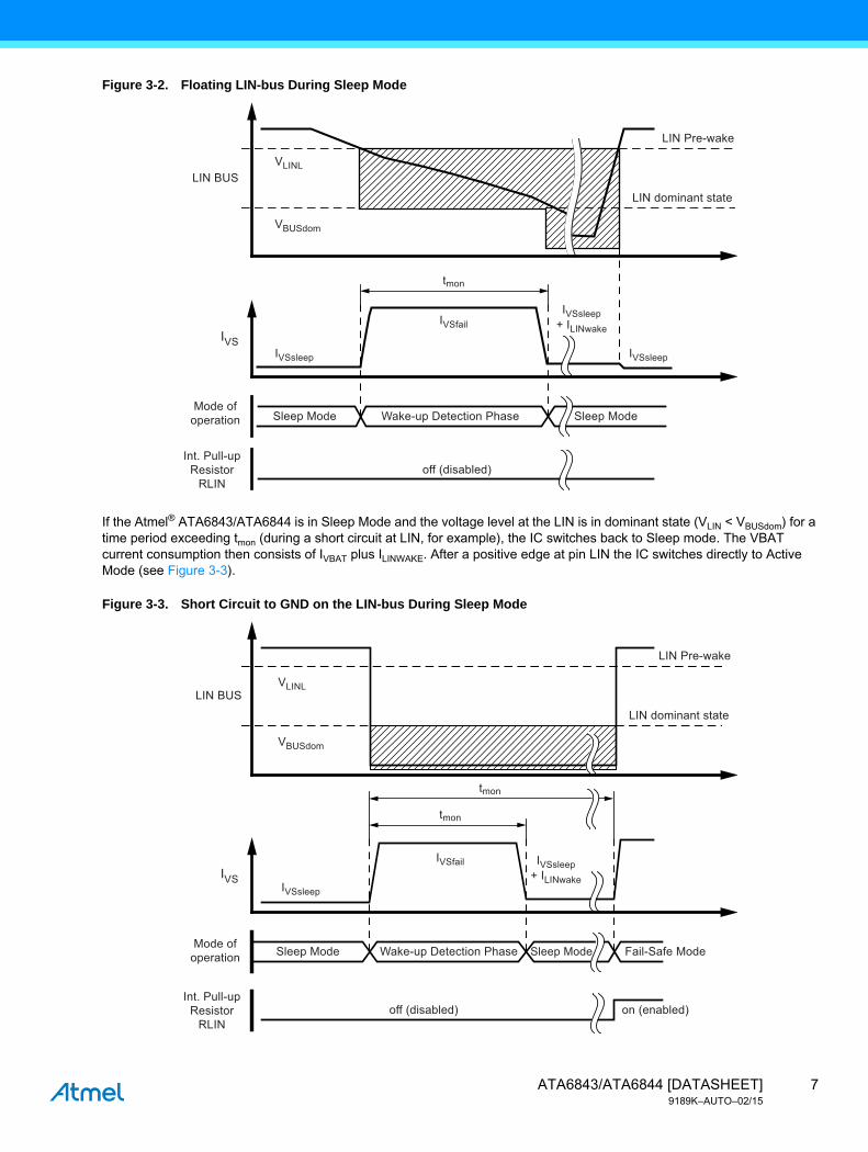
Figure 3-2. Floating LIN-bus During Sleep Mode
If the Atmel® ATA6843/ATA6844 is in Sleep Mode and the voltage level at the LIN is in dominant state (VLIN < VBUSdom) for a time period exceeding tmon (during a short circuit at LIN, for example), the IC switches back to Sleep mode. The VBAT current consumption then consists of IVBAT plus ILINWAKE. After a positive edge at pin LIN the IC switches directly to Active Mode (see Figure 3-3).
Figure 3-3. Short Circuit to GND on the LIN-bus During Sleep Mode
IVSsleep IVSsleep
IVSfail + ILINwake
IVSsleep
VBUSdom
VLINL
IVS
tmon
LIN Pre-wake
LIN dominant stateLIN BUS
Mode ofoperation
Int. Pull-upResistor
RLIN
Wake-up Detection Phase
off (disabled)
Sleep Mode Sleep Mode
Sleep Mode
IVSsleep
IVSfail+ ILINwake
IVSsleep
VBUSdom
VLINL
LIN Pre-wake
LIN dominant stateLIN BUS
IVS
Mode ofoperation
Int. Pull-upResistor
RLINoff (disabled) on (enabled)
Wake-up Detection PhaseSleep Mode Fail-Safe Mode
tmon
tmon
7ATA6843/ATA6844 [DATASHEET]9189K–AUTO–02/15
3.3 5V/3.3V VCC Regulator
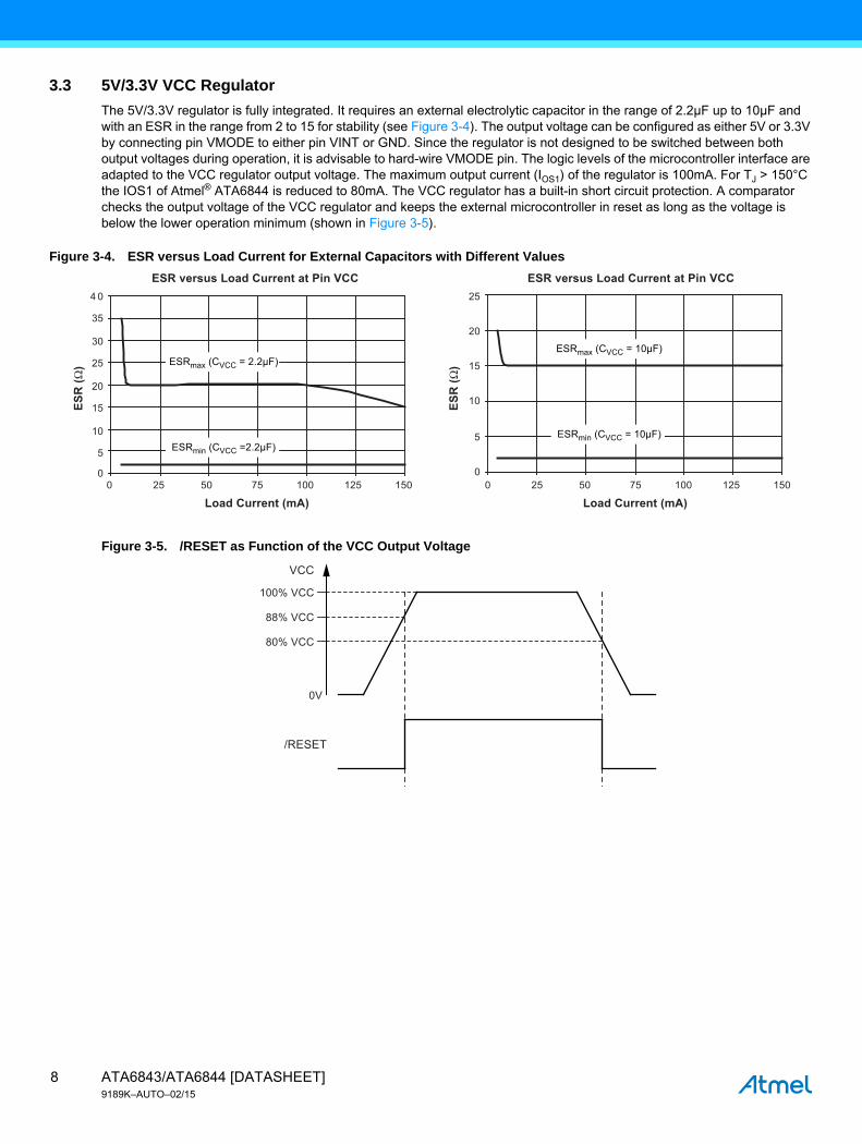
The 5V/3.3V regulator is fully integrated. It requires an external electrolytic capacitor in the range of 2.2µF up to 10µF and with an ESR in the range from 2 to 15 for stability (see Figure 3-4). The output voltage can be configured as either 5V or 3.3V by connecting pin VMODE to either pin VINT or GND. Since the regulator is not designed to be switched between both output voltages during operation, it is advisable to hard-wire VMODE pin. The logic levels of the microcontroller interface are adapted to the VCC regulator output voltage. The maximum output current (IOS1) of the regulator is 100mA. For TJ > 150°C the IOS1 of Atmel® ATA6844 is reduced to 80mA. The VCC regulator has a built-in short circuit protection. A comparator checks the output voltage of the VCC regulator and keeps the external microcontroller in reset as long as the voltage is below the lower operation minimum (shown in Figure 3-5).
Figure 3-4. ESR versus Load Current for External Capacitors with Different Values
Figure 3-5. /RESET as Function of the VCC Output Voltage
4 0
35
30
25
20
15
10
5
0
ESR
(Ω)
25
20
15
10
5
0
ESR
(Ω)
ESR versus Load Current at Pin VCC ESR versus Load Current at Pin VCC
0 25 50 75 100 125 150
Load Current (mA)0 25 50 75 100 125 150
Load Current (mA)
ESRmax (CVCC = 2.2µF)
ESRmin (CVCC =2.2µF)
ESRmax (CVCC = 10µF)
ESRmin (CVCC = 10µF)
100% VCC
0V
VCC
/RESET
80% VCC
88% VCC
ATA6843/ATA6844 [DATASHEET]9189K–AUTO–02/15
8

3.4 Reset and Watchdog Management
The watchdog timing is based on the trimmed internal watchdog oscillator. Its period time TOSC is determined by the external resistor RWD. A HIGH signal on WDEN pin enables the watchdog function; a LOW signal disables it. Since the WDEN pin is equipped with an internal pull-up resistor the watchdog is enabled by default. In order to keep the current consumption as low as possible the watchdog is switched off during Sleep Mode.
The timing diagram in Figure 3-6 shows the watchdog and external reset timing.
Figure 3-6. Timing Diagram of the Watchdog in Conjunction with the /RESET Signal
After power-up of the VCC regulator (VCC output exceeds 88% of its nominal value) /RESET output stays LOW for the timeout period tres (typical 10ms). Subsequently /RESET output switches to HIGH. During the following time td (typical 500ms) a rising edge at the input WD is expected otherwise another external reset will be triggered.
When the watchdog has been correctly triggered for the first time, normal watchdog operation begins. A normal watchdog cycle consists of two time sections t1 and t2 followed by a short pulse for the time tresshort at /RESET if no valid trigger has been applied at pin WD during t2. Rising edges on WD pin during t1 also cause a short pulse on /RESET. Start for such a cycle is always the time of the last rising edge either on WD pin or on /RESET pin.
If the watchdog is disabled (WDEN = LOW), only the initial reset for the time tres after power-up will be generated.
Additional resets will be generated if the VCC output voltage drops below 80% of its nominal value.
The following example demonstrates how to calculate the timing scheme for valid watchdog trigger pulses, which the external microcontroller has to provide in order to prevent undesired resets.
Example:
Using an external resistor RWD = 33k ±1% results in typical parameters as follows:
TOSC = 12.4µs
t1 = 980 TOSC = 12.1ms ±10%
t2 = 780 TOSC = 9.6ms ±10%
t1 + t2 = 21.7ms ±10%
Hence, the minimum time the external microcontroller has to wait before pin WD can be triggered is in worst case tmin = 1.1 t1 = 13.3ms. The maximum time for the watchdog trigger on WD pin is tmax = 0.9 (t1 + t2) = 19.5ms. Thus watchdog trigger input must remain within tmax – tmin = 6.2ms.
Watchdogtrigger edge
Reset and leadtime, no trigger
Watchdog cycle,no trigger
Watchdog cycle, triggerduring t2 window
Reset and lead time,trigger during lead time
tresshort
t1 t2t1tdtres td t1tres
t2
Watchdog triggerin t2 window
88% VCC
VCC
WD
/RESET
9ATA6843/ATA6844 [DATASHEET]9189K–AUTO–02/15
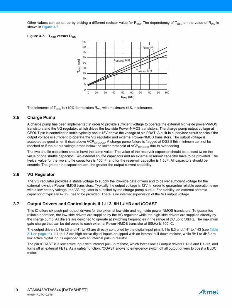
Other values can be set up by picking a different resistor value for RWD. The dependency of TOSC on the value of RWD isshown in Figure 3-7.
Figure 3-7. TOSC versus RWD
The tolerance of TOSC is ±10% for resistors RWD with maximum ±1% in tolerance.
3.5 Charge Pump
A charge pump has been implemented in order to provide sufficient voltage to operate the external high-side power-NMOS transistors and the VG regulator, which drives the low-side Power-NMOS transistors. The charge pump output voltage at CPOUT pin is controlled to settle typically about 15V above the voltage at pin PBAT. A built-in supervisor circuit checks if the output voltage is sufficient to operate the VG regulator and external Power-NMOS transistors. The output voltage is accepted as good when it rises above VCPCPGOOD. A charge pump failure is flagged at DG2 if this minimum can not be reached or if the output voltage drops below the lower threshold of VCPCPGOOD due to overloading.
The two shuffle capacitors should have the same value. The value of the reservoir capacitor should be at least twice the value of one shuffle capacitor. Two external shuffle capacitors and an external reservoir capacitor have to be provided. The typical value for the two shuffle capacitors is 100nF, and for the reservoir capacitor is 1.5µF. All capacitors should be ceramic. The greater the capacitors are, the greater the output current capability.
3.6 VG Regulator
The VG regulator provides a stable voltage to supply the low-side gate drivers and to deliver sufficient voltage for the external low-side Power-NMOS transistors. Typically the output voltage is 12V. In order to guarantee reliable operation even with a low battery voltage, the VG regulator is supplied by the charge pump output. For stability, an external ceramic capacitor of typically 470nF has to be provided. There is no internal supervision of the VG output voltage.
3.7 Output Drivers and Control Inputs IL1-IL3, /IH1-/IH3 and /COAST
This IC offers six push-pull output drivers for the external low-side and high-side power-NMOS transistors. To guarantee reliable operation, the low-side drivers are supplied by the VG regulator while the high-side drivers are supplied directly by the charge pump. All drivers are designed to operate at switching frequencies in the range of DC up to 50kHz. The maximum gate charge that can be delivered to each external Power-NMOS transistor at 50kHz is 100nC.
The output drivers L1 to L3 and H1 to H3 are directly controlled by the digital input pins IL1 to IL3 and /IH1 to /IH3 (see Table 3-1 on page 11). IL1 to IL3 are high active digital inputs equipped with an internal pull-down resistor, while /IH1 to /IH3 are low active digital inputs equipped with an internal pull-up resistor.
The pin /COAST is a low active input with internal pull-up resistor, which forces low all output drivers L1-L3 and H1-H3, and turns off all external FETs. As a safety function, /COAST allows to emergency switch off all output drivers to coast a BLDC motor.
4 0
4 5
35
30
25
20
15
10
5
010 20 4030 60 90807050 100
T OSC
(μs) TOSCmax (µs)
TOSCmin (µs)
TOSC (µs)
RWD (kΩ)
ATA6843/ATA6844 [DATASHEET]9189K–AUTO–02/15
10
To operate the output drivers properly the following requirements have to be fulfilled:
1. Device is in Active Mode.
2. In case of watchdog is enabled, at least one valid watchdog trigger has been accepted.
3. The voltage at pin PBAT lies within its operation range. Neither undervoltage nor overvoltage is present.
4. The charge pump output voltage has been accepted as good, thus it exceeded VCPCPGOOD.
5. No overtemperature shutdown has occurred.
6. /COAST is high
If a short circuit is detected by one of the sense inputs S1 to S3, the output drivers will be switched off after a blanking time tSC of typically 6 µs and the output DG1 will be flagged (see also Section 3.8 “Short Circuit Detection and Short Circuit Comparator Reference Input” on page 11). The output drivers will be enabled again and DG1 will be cleared with a rising edge at one of the control inputs IL1 to IL3, or falling edge at one of the control inputs /IH1 to /IH3.
Additional logic prevents short circuits due to switching on one power-NMOS transistor while the opposite one in the same branch is switched on already.
3.8 Short Circuit Detection and Short Circuit Comparator Reference Input
Short circuits in the motor bridge circuitry are sensed by S1 to S3 inputs. Internal comparators monitor the voltage differences between the drain and the source terminals of the external power-NMOS transistors and compare it to voltage VSCREF applied at pin SCREF. If one transistor switches on and its drain-source voltage exceeds VSCREF threshold after a blanking time tSC (see Figure 3-8 on page 12), a short circuit in this branch will be detected. In this case, the short-circuit detected output will be switched off immediately and pin DG1 will be set to HIGH. With a rising edge at any of the pins IL1 to IL3 or a falling edge at any of the pins /IH1 to /IH3, the diagnostic output DG1will be reset and the drivers switched on again.
Note, valid voltage range for short-circuit reference is 0.5V ≤ VSCREF ≤ 3.3V. Voltages outside this range will lead to incorrect short circuit thresholds. If pin SCREF is floating VSCREF will be set to approximately 2.5V by an integrated resistive voltage divider.
3.9 Cross Conduction Timer
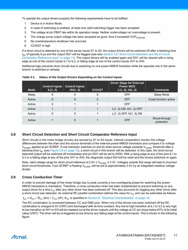
In order to prevent damage of the motor bridge due to peak currents a non-overlapping phase for switching the power-NMOS transistors is mandatory. Therefore, a cross conduction timer has been implemented to prevent switching on any output driver for a time tCC after any other driver has been switched off. This also accounts for toggling any other driver after a short circuit was detected. An external RC parallel combination defines the value for tCC and can be estimated as follows:
tCC = KCC RCC (k) CCC (nF), KCC is specified in Section 8. “Electrical Characteristics” on page 16.
The RC combination is connected between CC and GND pins. When one of the drivers has been switched off the RC combination is charged to 5V (VINT) and discharged with its time constant. Any low to high transition at IL1 to IL3 or any high to low transition at /IH1 to IH3 will be masked out at the driver outputs until the voltage at CC pin drops below 67% of its initial value (VINT). The timer will be re-triggered at any time by any falling edge at the control inputs. This is shown in the following figure.
Table 3-1. Status of the Output Drivers Depending on the Control Inputs
ModeControl Inputs
IL(1..3)Control Inputs
/IH(1..3) /COAST
Driver Stage for External Power MOS
L(1..3), H(1..3) Comments
Sleep X X X OFF Sleep Mode
Active X X 0 OFF Coast function active
Active 0 1 1 OFF
Active 1 1 1 L(1..3) ON, H(1..3) OFF
Active 0 0 1 L(1..3) OFF, H(1..3) ON
Active 1 0 1 OFFShoot-through
protection
11ATA6843/ATA6844 [DATASHEET]9189K–AUTO–02/15
Figure 3-8. Interaction of Short Circuit Detection and Cross Conduction Timer
At least 5k minimum and 5nF at maximum should be used as values for the RC combination. 10k is recommended. If the non-overlapping phase is controlled by the external microcontroller, it is possible to do without the external capacitor. The minimum time tCC is defined by the parasitic capacitance at CC pin.
3.10 Diagnostic Outputs DG1 - DG3
As mentioned in the sections above, the diagnostic outputs DG1 to DG3 are used to signal failures. This is summarized in the following table.
Note: This is only valid for VCC > VtHRESHLow. Otherwise all diagnostic outputs will be tristated.
In order to differentiate between LIN and EN wake-up, DG1 output will be set to LOW or HIGH respectively. LOW indicates wake-up by LIN, HIGH indicates wake-up by EN. DG1 output will be cleared by the first valid watchdog trigger after wake-up or by the first rising edge at IL1 to IL3 if the watchdog is disabled or by the first falling edge at /IH1 to /IH3if the watchdog is disabled.
tcc tcc tcc
L1
/IH1
IL3
CC
L3
H1
IL1
VCC = 67% VVINT
VCC = VVINT
Ignore VS1for tSC = 6µs
Shut offif VS1 > 4V
Ignore VPBAT - VS1for tSC = 6µs
Shut offif VPBAT - VS1 > 4V
Ignore VS3for tSC = 6µs
Shut offif VS3 > 4V
Table 3-2. Status of the Diagnostic Outputs (Normal Operation)
Device Status Diagnostic Outputs
CommentsCPOK OT1 OV UV SC DG1 DG2 DG3
0 X X X X – 1 – Charge pump failure
X 1 X X X – – 1 Overtemperature prewarning
X X 1 X X – 1 – Overvoltage
X X X 1 X – 1 – Undervoltage
X X X X 1 1 – – Short circuit
Note: X represents: no effect)OT1: overtemperature warningOV: overvoltage of PBATUV: undervoltage of PBATSC: short circuitCPOK: charge pump OK
ATA6843/ATA6844 [DATASHEET]9189K–AUTO–02/15
12
3.11 LIN Transceiver
Atmel® ATA6843 and Atmel ATA6844 include a fully integrated LIN transceiver complying with LIN specification 2.1 and SAEJ2602 2. The transceiver consists of a low-side driver with slew rate control, wave shaping, current limiting, and a high voltage comparator followed by a debouncing unit in the receiver.
During transmission, the data applied at pin TXD will be transferred to the bus driver to generate a bus signal on LIN pin. TXD input has an internal pull-up resistor.
To minimize the electromagnetic emission of the bus line, the bus driver has a built-in slew rate control and wave-shaping unit. The transmission will be aborted by a thermal shutdown or by a transition to Sleep Mode.
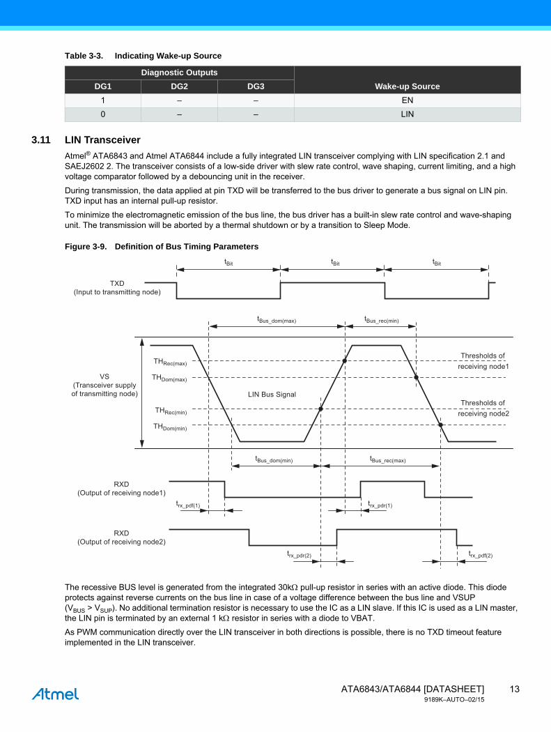
Figure 3-9. Definition of Bus Timing Parameters
The recessive BUS level is generated from the integrated 30k pull-up resistor in series with an active diode. This diode protects against reverse currents on the bus line in case of a voltage difference between the bus line and VSUP (VBUS > VSUP). No additional termination resistor is necessary to use the IC as a LIN slave. If this IC is used as a LIN master, the LIN pin is terminated by an external 1 k resistor in series with a diode to VBAT.
As PWM communication directly over the LIN transceiver in both directions is possible, there is no TXD timeout feature implemented in the LIN transceiver.
Table 3-3. Indicating Wake-up Source
Diagnostic Outputs
Wake-up SourceDG1 DG2 DG3
1 – – EN
0 – – LIN
TXD(Input to transmitting node)
VS(Transceiver supplyof transmitting node)
RXD(Output of receiving node1)
RXD(Output of receiving node2)
LIN Bus Signal
Thresholds ofreceiving node1
Thresholds ofreceiving node2
tBus_rec(max)
trx_pdr(1)
trx_pdf(2)trx_pdr(2)
trx_pdf(1)
tBus_dom(min)
tBus_dom(max)
THRec(max)
THDom(max)
THRec(min)
THDom(min)
tBus_rec(min)
tBit tBittBit
13ATA6843/ATA6844 [DATASHEET]9189K–AUTO–02/15

4. Absolute Maximum Ratings
Stresses beyond those listed under “Absolute Maximum Ratings” may cause permanent damage to the device. This is a stress rating only and functional operation of the device at these or any other conditions beyond those indicated in the operational sections of this specification is not implied. Exposure to absolute maximum rating conditions for extended periods may affect device reliability.
All voltages are referenced to pin GND. (xxx) Values for the Atmel® ATA6844.
Parameters Pin Symbol Min. Max. Unit
Input voltage PGND VPGND –0.3 +0.3 V
Negative input current VBAT IVBAT –15 mA
Negative input current PBAT IPBAT –20 mA
Supply voltage VBAT VVBAT +40 V
Supply voltage PBAT VPBAT +40 V
Logic output voltage/RESET, DG1,
DG2, DG3, RXDV/RESET, VDG1, VDG2,
VDG3, VRXD –0.3 VVCC + 0.3 V
Logic input voltageIL1-3, /IH1-3, WD, WDD, SLEEP, TXD
VIL1-3, V/IH1-3, VWD, VSLEEP, VTXD
–0.3 VVCC + 0.3 V
Output voltage VINT, VCC VINT, VVVCC –0.3 +5.5 V
Analog input voltage RWD, CC, SCREF VRWD , VCC, VSCREF –0.3 VVCC + 0.3 V
Digital input voltage EN VEN –0.3 VVBAT + 0.3 V
Digital input voltage VMODE VVMODE –0.3 VVINT + 0.3 V
Output voltage VG VVG +16 V
Input voltage LIN VVLIN –27 VVBAT + 2 V
Output voltage S1, S2, S3 VS1, VS2, VS3 (–6) +40 V
Output voltage L1, L2, L3 VL1, VL2, VL3 VPGND – 0.3 VVG + 0.3 V
Output voltage H1, H2, L3 VH1, VH2, VH3 VS1, 2, 3 – 1 VS1, 2, 3 + 16 V
Charge pump CPLO1, 2 VCPLO1, VCPLO2 VPBAT + 0.3 V
Charge pump CPHI1, 2 VCPHI1, VCPHI2 VCPOUT + 0.3 V
Output voltage CPOUT VCPOUT +52 V
Storage temperature TStorage –55 +150 °C
Reverse current
CPLOx, CPHIx, VG, CPOUT, Sx
ICPLOx_R, ICPHIx_R, IVG_R, ICPOUT_R, ISx_R
–2 mA
Lx, Hx ILx_R, IHx_R –1 mA
Note: Estimated values take TJ > 150°C into account.
5. Thermal Resistance
Parameters Symbol Value Unit
Thermal resistance junction to heat slug Rthjc < 5 K/W
Thermal resistance junction to ambient when heat slug is soldered to PCB
Rthja 25 K/W
ATA6843/ATA6844 [DATASHEET]9189K–AUTO–02/15
14
Static latch-up tested according to AEC-Q100-004 and JESD78.
● 3 to 6 samples, 0 failures
● Electrical post-stress testing at room temperature
In test, the voltage at the pins VBAT, LIN, CP, VBATSW, Hx, and Sx must not exceed 45V when not able to drive the specified current.
6. Operating Range
The operating conditions define the limits for functional operation and parametric characteristics of the device. Functionality outside these limits is not implied unless otherwise stated explicitly. (xxx) Values for the Atmel® ATA6844
Parameters Symbol Min Max Unit
Operating supply voltage(1) VVBAT 5.5 VTHOV V
Operating supply voltage(2) VVBAT 4.3 5.5 V
Operating supply voltage(3) VVBAT VTHOV 40 V
Ambient temperature range TA –40 +150 °C
Junction temperature range TJ –40 +150 (200) °C
Notes: 1. Full functionality
2. Output drivers are switched off, extended range for parameters for voltage regulators
3. Output drivers and charge pump are switched off
7. Noise and Surge Immunity, ESD and Latch-up
Parameters Standard and Test Conditions Value
Conducted interferences ISO 7637-1 Level 4(1)
Conducted disturbances CISP25 Level 5
ESD according to IBEE LIN EMC- Pins LIN, PBAT, VBAT- Pin EN (33k serial resistor)
Test specification 1.0 following IEC 61000-4-2±6kV±5kV
ESD HBM with 1.5k/100pF
ESD- STM5.1-2001JESD22-A114E 2007CEI/IEC 60749-26: 2006AEC-Q100-002-Ref_D
±2kV
ESD HBM with 1.5k/100pFPins EN, LIN, PBAT, VBAT against GND
ESD- STM5.1-2001JESD22-A114E 2007CEI/IEC 60749-26: 2006AEC-Q100-002-Ref_D
±8kV
ESD CDM (field induced method) ESD STM5.3.1 - 1999 ±500V
Note: 1. Test pulse 5: Vbat max = 40V
15ATA6843/ATA6844 [DATASHEET]9189K–AUTO–02/15
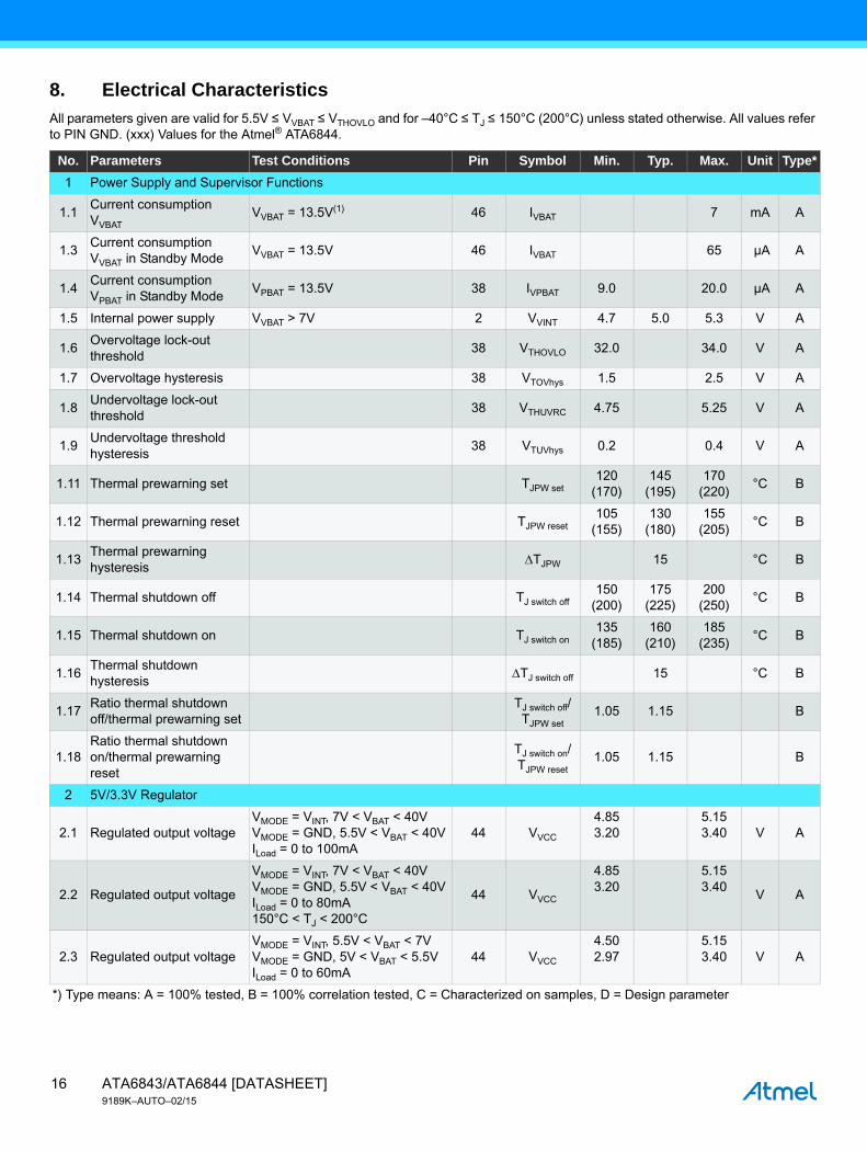
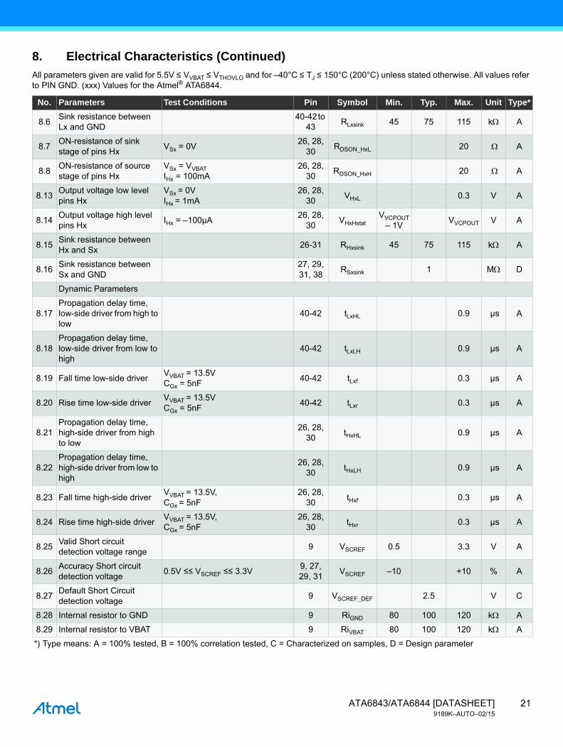
8. Electrical Characteristics
All parameters given are valid for 5.5V ≤ VVBAT ≤ VTHOVLO and for –40°C ≤ TJ ≤ 150°C (200°C) unless stated otherwise. All values refer to PIN GND. (xxx) Values for the Atmel® ATA6844.
No. Parameters Test Conditions Pin Symbol Min. Typ. Max. Unit Type*
1 Power Supply and Supervisor Functions
1.1Current consumption VVBAT
VVBAT = 13.5V(1) 46 IVBAT 7 mA A
1.3Current consumption VVBAT in Standby Mode
VVBAT = 13.5V 46 IVBAT 65 µA A
1.4Current consumption VPBAT in Standby Mode
VPBAT = 13.5V 38 IVPBAT 9.0 20.0 µA A
1.5 Internal power supply VVBAT > 7V 2 VVINT 4.7 5.0 5.3 V A
1.6Overvoltage lock-out threshold
38 VTHOVLO 32.0 34.0 V A
1.7 Overvoltage hysteresis 38 VTOVhys 1.5 2.5 V A
1.8Undervoltage lock-out threshold
38 VTHUVRC 4.75 5.25 V A
1.9Undervoltage threshold hysteresis
38 VTUVhys 0.2 0.4 V A
1.11 Thermal prewarning set TJPW set120
(170)145
(195)170
(220)°C B
1.12 Thermal prewarning reset TJPW reset105
(155)130
(180)155
(205)°C B
1.13Thermal prewarning hysteresis
TJPW 15 °C B
1.14 Thermal shutdown off TJ switch off150
(200)175
(225)200
(250)°C B
1.15 Thermal shutdown on TJ switch on135
(185)160
(210)185
(235)°C B
1.16Thermal shutdown hysteresis
TJ switch off 15 °C B
1.17Ratio thermal shutdown off/thermal prewarning set
TJ switch off/ TJPW set
1.05 1.15 B
1.18Ratio thermal shutdown on/thermal prewarning reset
TJ switch on/TJPW reset
1.05 1.15 B
2 5V/3.3V Regulator
2.1 Regulated output voltageVMODE = VINT, 7V < VBAT < 40VVMODE = GND, 5.5V < VBAT < 40VILoad = 0 to 100mA
44 VVCC
4.853.20
5.153.40 V A
2.2 Regulated output voltage
VMODE = VINT, 7V < VBAT < 40VVMODE = GND, 5.5V < VBAT < 40VILoad = 0 to 80mA 150°C < TJ < 200°C
44 VVCC
4.853.20
5.153.40
V A
2.3 Regulated output voltageVMODE = VINT, 5.5V < VBAT < 7VVMODE = GND, 5V < VBAT < 5.5VILoad = 0 to 60mA
44 VVCC
4.502.97
5.153.40 V A
*) Type means: A = 100% tested, B = 100% correlation tested, C = Characterized on samples, D = Design parameter
ATA6843/ATA6844 [DATASHEET]9189K–AUTO–02/15
16
2.4 Regulated output voltage
VMODE = VINT, 5.5V < VBAT < 7VVMODE = GND, 5V < VBAT < 5.5VILoad = 0 to 50mA 150°C < TJ < 200°C
44 VVCC
4.502.97
5.153.40
V A
2.5 Line regulationVMODE = VINT, 7V < VBAT < 40VVMODE = GND, 5.5V < VBAT < 40VILoad = 50mA, –40°C < TJ < 150°C
445050 mV A
2.6 Load regulation
VMODE = VINT, VBAT > 7VVMODE = GND, VBAT > 5.5VILoad = 0 to 100mAILoad = 0 to 80mA, 150°C < TJ < 200°C
44
5050
mV A
2.7 Output current limitVMODE = VINT, VBAT > 7VVMODE = GND, VBAT > 5.5VILoad at RESET
44 IOS1
100100
360360 mA A
2.8 Output current limit
VMODE = VINT, VBAT > 7VVMODE = GND, VBAT > 5.5VILoad at RESET, 150°C < TJ < 200°C
44 IOS1
7070
360360
mA C
2.12 HIGH threshold VMODE 1 VVMODE H 4.0 V A
2.13 LOW threshold VMODE 1 VVMODE L 0.7 V A
3 Reset and Watchdog
3.1VCC threshold voltage level for /RESET
VMODE = VINT (VMODE = GND)
5 VtHRESHLow3.82.5
4.22.8
VAB
3.2 HysteresisVMODE = VINT (VMODE = GND)
5 HYSRESth0.2
0.130.60.4
VAB
3.3 Length of pulse at /RESET 5 tres 8 12 ms A
3.4Length of short pulse at /RESET
5 tresshort 1.6 2.4 ms A
3.5 Wait for the first WD trigger 5 td 400 600 ms A
3.6Time for VCC < VtHRESL before activating /RESET
5 tdelayRESL 2 µs C
3.8 Watchdog oscillator period RRWD = 33k ±1% (5) TOSC 11.09 13.55 µs A
3.12 Close window (5) t1980 TOSC
A
3.13 Open window (5) t2780 TOSC
A
3.14Output low-level at pin /RESET
IOLRES = 1mA 5 VOLRES 0.4 V A
3.15Internal pull-up resistor at pin /RESET
5 RPURES 5 10 15 k D
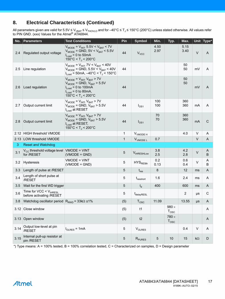
8. Electrical Characteristics (Continued)
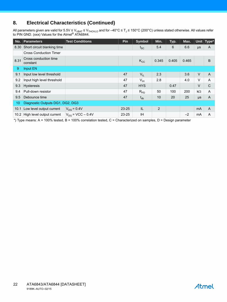
All parameters given are valid for 5.5V ≤ VVBAT ≤ VTHOVLO and for –40°C ≤ TJ ≤ 150°C (200°C) unless stated otherwise. All values refer to PIN GND. (xxx) Values for the Atmel® ATA6844.
No. Parameters Test Conditions Pin Symbol Min. Typ. Max. Unit Type*
*) Type means: A = 100% tested, B = 100% correlation tested, C = Characterized on samples, D = Design parameter
17ATA6843/ATA6844 [DATASHEET]9189K–AUTO–02/15
4 LIN Transceiver
4.1 Low-level output currentNormal mode; VLIN = 0V, VRXD = 0.4V
22 ILRXD 2 mA D
4.2 High-level output currentNormal mode; VLIN = VBATVRXD = VCC – 0.4V
22 IHRXD –2 mA D
4.3Driver recessive output voltage
VTXD = VCC; ILIN = 0mA 13 VBUSrec0.9 VBAT
V A
4.4Driver dominant voltageVBUSdom_DRV_LoSUP
VVBAT = 7.3VRload = 500
13 V_LoSUP 1.2 V A
4.5Driver dominant voltageVBUSdom_DRV_HiSUP
VVBAT = 18VRload = 500
13 V_HiSUP 2 V A
4.6Driver dominant voltageVBUSdom_DRV_LoSUP
VVBAT = 7.3VRload = 1000 13 V_LoSUP_1k 0.6 V A
4.7Driver dominant voltageVBUSdom_DRV_HiSUP
VVBAT = 18VRload = 1000
13 V_HiSUP_1k_ 0.8 V A
4.8 Pull up resistor to VS Serial diode required 13 RLIN 20 47 k A
4.9 Current limitation VBUS = VBAT_max 13 IBUS_LIM 50 200 mA A
4.10Input leakage current at the receiver including pull-up resistor as specified
Input leakage currentdriver offVBUS = 0VVBAT = 12V
13 IBUS_PAS_dom –1 mA A
4.11Leakage current LIN recessive
Driver off8V < VBAT < 18V8V < VBUS < 18VVBUS = VBAT
13 IBUS_PAS_rec 20 µA A
4.12
Leakage current at ground lossControl unit disconnected from groundLoss of local ground must not affect communication in the residual network
GNDDevice = VSVBAT = 12V0V < VBUS < 18V
13 IBUS_NO_gnd –1 +1 mA A
4.13
Node has to sustain the current that can flow under this condition. Bus must remain operational under this condition
VBAT disconnected VSUP_Device = GND0V < VBUS < 18V
13 IBUS 100 µA A
4.14Center of receiver threshold
VBUS_CNT = (Vth_dom + Vth_rec)/2
13 VBUS_CNT0.475 VVBAT
0.5 VVBAT
0.525 VVBAT
V A
4.15 Receiver dominant state VEN = 5V 13 VBUSdom0.4 VVBAT
V A
4.16 Receiver recessive state VEN = 5V 13 VBUSrec0.6 VVBAT
V A
4.17 Receiver input hysteresis VHYS = Vth_rec – Vth_dom 13 VBUShys0.175 VVBAT
V A
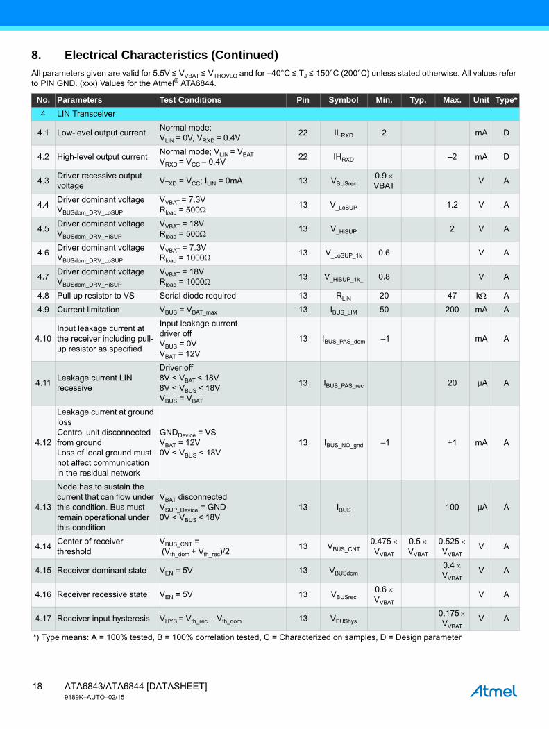
8. Electrical Characteristics (Continued)
All parameters given are valid for 5.5V ≤ VVBAT ≤ VTHOVLO and for –40°C ≤ TJ ≤ 150°C (200°C) unless stated otherwise. All values refer to PIN GND. (xxx) Values for the Atmel® ATA6844.
No. Parameters Test Conditions Pin Symbol Min. Typ. Max. Unit Type*
*) Type means: A = 100% tested, B = 100% correlation tested, C = Characterized on samples, D = Design parameter
ATA6843/ATA6844 [DATASHEET]9189K–AUTO–02/15
18

4.18 Duty cycle 1
7V < VVBAT < 18VTHrec(max) = 0.744 VVBATTHDom(max) = 0.581 VVBATtBit = 50µsD1 = tBus_rec(min)/(2 tBit)Load1: 1nF + 1kLoad2: 10nF + 500
13 D1 0.396 A
4.19 Duty cycle 2
7V < VVBAT < 18VTHrec(min) = 0.422 VVBATTHDom(min) = 0.284 VVBATtBit = 50µsD2 = tBus_rec(max)/(2×tBit)Load1: 1nF + 1kLoad2: 10nF + 500
13 D2 0.581 A
4.20 Duty cycle 3
7V < VVBAT < 18VTHrec(max) = 0.778 VVBATTHDom(max) = 0.616 VVBATtBit = 96µsD3 = tBus_rec(min)/(2 tBit)Load1: 1nF + 1kLoad2: 10nF + 500
13 D3 0.417 A
4.21 Duty cycle 4
7V < VVBAT < 18VTHrec(max) = 0.389 VVBATTHDom(max) = 0.251 VVBATtBit = 96µsD4 = tBus_rec(min)/(2 tBit)Load1: 1nF + 1kLoad2: 10nF + 500
13 D4 0.590 A
4.22Receiver propagation delay
7V < VVBAT < 18Vtrec_pd = max(trx_pdr, trx_pdf)
22 trx_pd 6 µs A
4.23Symmetry of receiver propagation delay rising edge minus falling edge
7V < VVBAT < 18Vtrx_sym = trx_pdr – trx_pdf
22 trx_sym –2 +2 µs A
4.24Dominant time for wake-up via LIN Bus
VLIN = 0V 13 TBUS 30 90 150 µs A
4.25Monitoring time for wake-up over LIN Bus
13 Tmon 6 10 15 ms B
4.26Pre-wake detection LIN Low-Level Input Voltage
Switches the LIN receiver on 13 VLINL –27VVBAT –
3.3V A
4.27Pre-wake detection LIN High-Level Input Voltage
13 VLINHVVBAT –
2VVBAT +
0.3V A
4.28LIN Pre-Wake pull-up current
VVBAT < 27VVLIN = 0V
13 ILINWake –30 –10 µA A
4.29Capacitance on LIN Pin to GND
13 CLIN 10 pF D
8. Electrical Characteristics (Continued)
All parameters given are valid for 5.5V ≤ VVBAT ≤ VTHOVLO and for –40°C ≤ TJ ≤ 150°C (200°C) unless stated otherwise. All values refer to PIN GND. (xxx) Values for the Atmel® ATA6844.
No. Parameters Test Conditions Pin Symbol Min. Typ. Max. Unit Type*
*) Type means: A = 100% tested, B = 100% correlation tested, C = Characterized on samples, D = Design parameter
19ATA6843/ATA6844 [DATASHEET]9189K–AUTO–02/15
5 Control Inputs WD, WDEN, SLEEP, TXD, IL1-3, /IH1-3, /COAST
5.1 Input low-level threshold6-8, 15-21, 48
VIL0.3 VVCC
V A
5.2 Input high-level threshold6-8, 15-21, 48
VIH0.7 VVCC
V A
5.3 Hysteresis6-8, 15-21, 48
HYS 0.3 C
5.4 Pull-down resistor WD, SLEEP, IL1-36, 8, 16, 18, 20
RPD 25 50 100 k A
5.5 Pull-up resistor WDEN, TXD, /IH1-3, /COAST7, 15, 17, 19, 21, 48
RPU 25 50 100 k A
5.7 Debounce time SLEEP 8 tgotosleep 9 10 11 µs A
6 Charge Pump
6.1 Charge pump voltage
VVBAT > 7VILoadCPOUT = 0AILoadVG = 0ACCP1,2 = 47nFCCPOUT = 220nF
32 VCPOUTVVBAT+ 11V
VVBAT+ 18
V A
6.2 Charge pump voltage
VVBAT > 7VILoadCPOUT = 7.5mA, ILoadVG = 0ACCP1,2 = 47nFCCPOUT = 220nF
32 VCPOUTVVBAT +10V
V A
6.3Period charge pump oscillator
TCP 2.5 µs B
6.4Charge pump output voltage for active drivers
32 VCPCPGOOD 5.25 8.0 V A
7 VG Regulator
7.1VG Regulator Output Voltage
VBAT = 13.5VVCPOUT = 20VILoadVG = 7.5mA
39 VVG 11 12.5 14 V A
7.2VG Regulator Line Regulation
VBAT = 13.5VVCPOUT1 = 20V, VCPOUT2 = 35VILoadVG = 7.5mA
39 VVG_Line 100 mV A
7.3VG Regulator Load Regulation
VBAT = 13.5VVCPOUT = 25VILoadVG1 = 1mA, ILoadVG2 = 60mA
39 VVG_Load 100 mV A
8 H-bridge Driver
8.1Low-side driver HIGH output voltage
40-42 VLxH VVG V D
8.2ON-resistance of sink stage of pins Lx
ILX = 100mA 40-42 RDSON_LxL 20 A
8.3ON-resistance of source stage of pins Lx
ILX = 100mA 40-42 RDSON_LxH 20 A
8. Electrical Characteristics (Continued)
All parameters given are valid for 5.5V ≤ VVBAT ≤ VTHOVLO and for –40°C ≤ TJ ≤ 150°C (200°C) unless stated otherwise. All values refer to PIN GND. (xxx) Values for the Atmel® ATA6844.
No. Parameters Test Conditions Pin Symbol Min. Typ. Max. Unit Type*
*) Type means: A = 100% tested, B = 100% correlation tested, C = Characterized on samples, D = Design parameter
ATA6843/ATA6844 [DATASHEET]9189K–AUTO–02/15
20
8.6Sink resistance between Lx and GND
40-42 to 43
RLxsink 45 75 115 k A
8.7ON-resistance of sink stage of pins Hx
VSx = 0V26, 28,
30RDSON_HxL 20 A
8.8ON-resistance of source stage of pins Hx
VSx = VVBATIHx = 100mA
26, 28, 30
RDSON_HxH 20 A
8.13Output voltage low level pins Hx
VSx = 0V IHx = 1mA
26, 28, 30
VHxL 0.3 V A
8.14Output voltage high level pins Hx
IHx = –100µA26, 28,
30VHxHstat
VVCPOUT – 1V
VVCPOUT V A
8.15Sink resistance between Hx and Sx
26-31 RHxsink 45 75 115 k A
8.16Sink resistance between Sx and GND
27, 29, 31, 38
RSxsink 1 M D
Dynamic Parameters
8.17Propagation delay time, low-side driver from high to low
40-42 tLxHL 0.9 µs A
8.18Propagation delay time, low-side driver from low to high
40-42 tLxLH 0.9 µs A
8.19 Fall time low-side driverVVBAT = 13.5VCGx = 5nF
40-42 tLxf 0.3 µs A
8.20 Rise time low-side driverVVBAT = 13.5VCGx = 5nF
40-42 tLxr 0.3 µs A
8.21Propagation delay time, high-side driver from high to low
26, 28, 30
tHxHL 0.9 µs A
8.22Propagation delay time, high-side driver from low to high
26, 28, 30
tHxLH 0.9 µs A
8.23 Fall time high-side driverVVBAT = 13.5V,CGx = 5nF
26, 28, 30
tHxf 0.3 µs A
8.24 Rise time high-side driverVVBAT = 13.5V,CGx = 5nF
26, 28, 30
tHxr 0.3 µs A
8.25Valid Short circuit detection voltage range
9 VSCREF 0.5 3.3 V A
8.26Accuracy Short circuit detection voltage
0.5V ≤≤ VSCREF ≤≤ 3.3V9, 27, 29, 31
VSCREF –10 +10 % A
8.27Default Short Circuit detection voltage
9 VSCREF_DEF 2.5 V C
8.28 Internal resistor to GND 9 RiGND 80 100 120 k A
8.29 Internal resistor to VBAT 9 RiVBAT 80 100 120 k A
8. Electrical Characteristics (Continued)
All parameters given are valid for 5.5V ≤ VVBAT ≤ VTHOVLO and for –40°C ≤ TJ ≤ 150°C (200°C) unless stated otherwise. All values refer to PIN GND. (xxx) Values for the Atmel® ATA6844.
No. Parameters Test Conditions Pin Symbol Min. Typ. Max. Unit Type*
*) Type means: A = 100% tested, B = 100% correlation tested, C = Characterized on samples, D = Design parameter
21ATA6843/ATA6844 [DATASHEET]9189K–AUTO–02/15
8.30 Short circuit blanking time tSC 5.4 6 6.6 µs A
Cross Conduction Timer
8.31Cross conduction time constant
KCC 0.345 0.405 0.465 B
9 Input EN
9.1 Input low level threshold 47 VIL 2.3 3.6 V A
9.2 Input high level threshold 47 VIH 2.8 4.0 V A
9.3 Hysteresis 47 HYS 0.47 V C
9.4 Pull-down resistor 47 RPD 50 100 200 k A
9.5 Debounce time 47 tdb 10 20 25 µs A
10 Diagnostic Outputs DG1, DG2, DG3
10.1 Low level output current VDG = 0.4V 23-25 IL 2 mA A
10.2 High level output current VDG = VCC – 0.4V 23-25 IH –2 mA A
8. Electrical Characteristics (Continued)
All parameters given are valid for 5.5V ≤ VVBAT ≤ VTHOVLO and for –40°C ≤ TJ ≤ 150°C (200°C) unless stated otherwise. All values refer to PIN GND. (xxx) Values for the Atmel® ATA6844.
No. Parameters Test Conditions Pin Symbol Min. Typ. Max. Unit Type*
*) Type means: A = 100% tested, B = 100% correlation tested, C = Characterized on samples, D = Design parameter
ATA6843/ATA6844 [DATASHEET]9189K–AUTO–02/15
22
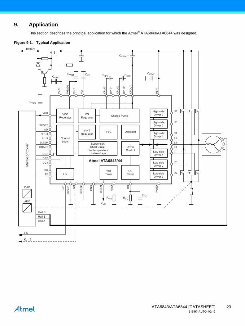
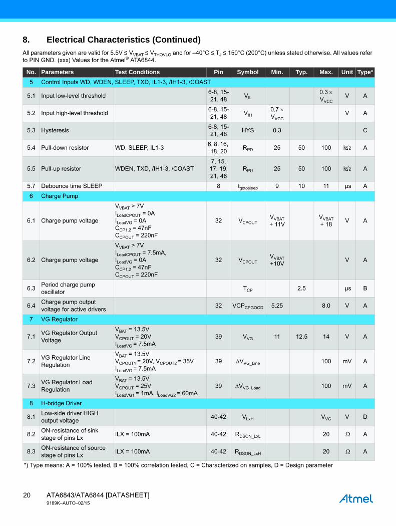
9. Application
This section describes the principal application for which the Atmel® ATA6843/ATA6844 was designed.
Figure 9-1. Typical Application
Supervisor:Short Circuit
OvertemperatureUndervoltage
Charge Pump
CCTimer
WDTimer
VBG
LIN
KL 15
LIN
DAC
Hall CHall BHall A
Atmel ATA6843/44
Oscillator
DriverControl
VINTRegulator
ControlLogic
VGRegulator
LIN
VBAT
Mic
roco
ntro
ller
VIN
T
CPH
I1
CPH
I2
CPL
O1
PBAT
CPO
UT
CPL
O2
VGVMO
DE
High-sideDriver 1
High-sideDriver 2
High-sideDriver 3
CCP1
CCPOUT
CVINT
CVCC
CVG
RWD
CCP2CPBAT
CVBAT
VCCRegulator
Low-sideDriver 3
Low-sideDriver 2
Low-sideDriver 1
+
L2
L1
L3
H2
H3
Battery
DG3
/RESET
DG2
DG1
WD
/IH1-3
SLEEP
COAST
IL1-3
TX
RX
VCC
H1
S2
S3
S1
LIN
GN
D
WD
EN
GN
D
PGN
D
RW
D
CC
SCR
EF
RCCCCC
VCCADC
EN
23ATA6843/ATA6844 [DATASHEET]9189K–AUTO–02/15
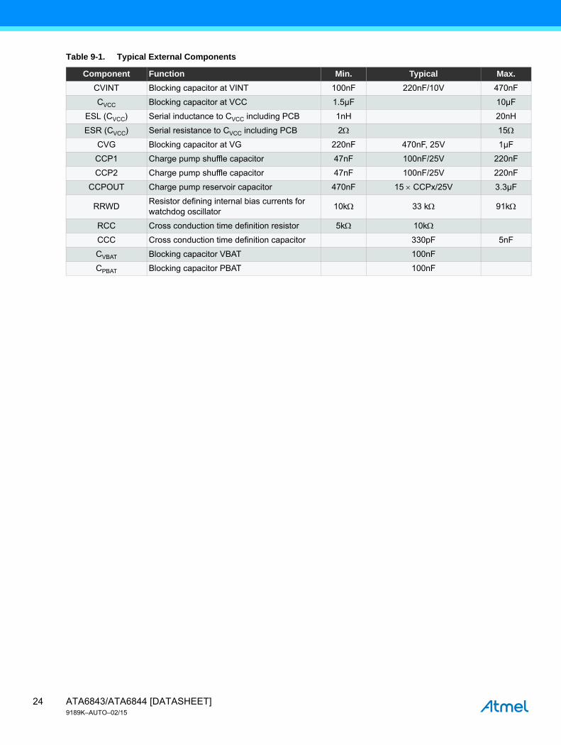
Table 9-1. Typical External Components
Component Function Min. Typical Max.
CVINT Blocking capacitor at VINT 100nF 220nF/10V 470nF
CVCC Blocking capacitor at VCC 1.5µF 10µF
ESL (CVCC) Serial inductance to CVCC including PCB 1nH 20nH
ESR (CVCC) Serial resistance to CVCC including PCB 2 15
CVG Blocking capacitor at VG 220nF 470nF, 25V 1µF
CCP1 Charge pump shuffle capacitor 47nF 100nF/25V 220nF
CCP2 Charge pump shuffle capacitor 47nF 100nF/25V 220nF
CCPOUT Charge pump reservoir capacitor 470nF 15 CCPx/25V 3.3µF
RRWDResistor defining internal bias currents for watchdog oscillator
10k 33 k 91k
RCC Cross conduction time definition resistor 5k 10k
CCC Cross conduction time definition capacitor 330pF 5nF
CVBAT Blocking capacitor VBAT 100nF
CPBAT Blocking capacitor PBAT 100nF
ATA6843/ATA6844 [DATASHEET]9189K–AUTO–02/15
24
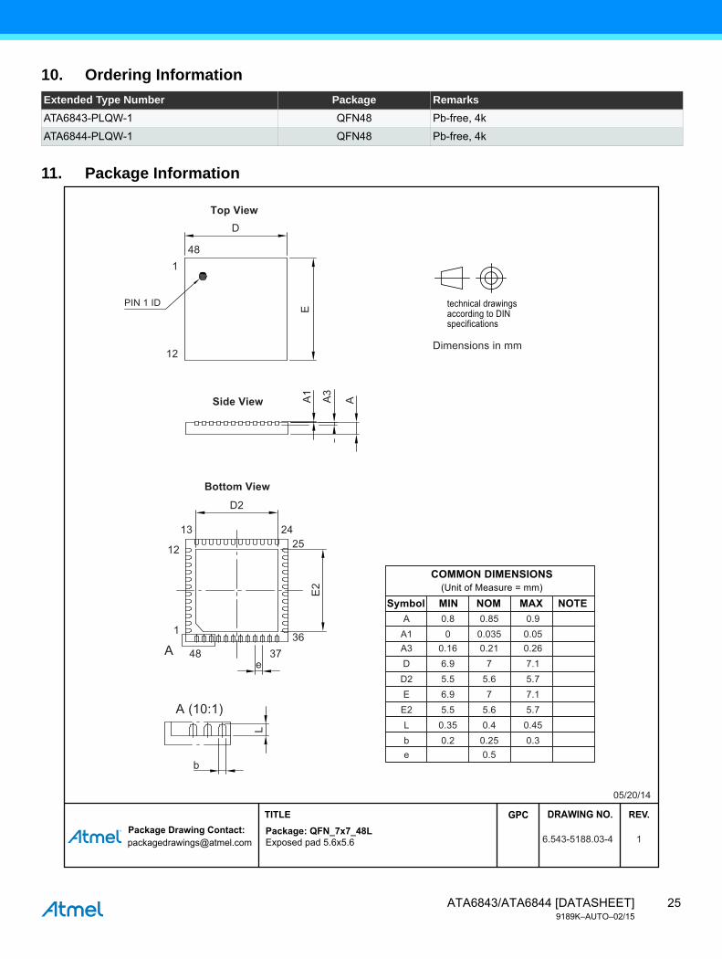
11. Package Information
10. Ordering Information
Extended Type Number Package Remarks
ATA6843-PLQW-1 QFN48 Pb-free, 4k
ATA6844-PLQW-1 QFN48 Pb-free, 4k
Package Drawing Contact:[email protected]
GPC DRAWING NO. REV. TITLE
6.543-5188.03-4 1
05/20/14
Package: QFN_7x7_48LExposed pad 5.6x5.6
COMMON DIMENSIONS(Unit of Measure = mm)
MIN NOM NOTEMAXSymbol
Dimensions in mm
specificationsaccording to DINtechnical drawings
0.035 0.050A1
7 7.16.9E
0.25 0.30.2b0.5e
0.4 0.450.35L5.6 5.75.5E2
5.6 5.75.5D27 7.16.9D
0.21 0.260.16A3
0.85 0.90.8A
b
L
A (10:1)
A
D
1
12
48
PIN 1 ID E
Top View
AA3A1E2
Side View
Bottom View
e
D2
48 37
13
12
1
2425
36
25ATA6843/ATA6844 [DATASHEET]9189K–AUTO–02/15
12. Revision History
Please note that the following page numbers referred to in this section refer to the specific revision mentioned, not to this document.
Revision No. History
9189K-AUTO-02/15Section 10 “Ordering Information” on page 25 updated
Section 11 “Package Information” on page 25 updated
9189J-AUTO-05/14 Section 8 “Electrical Characteristics” numbers 8.4 and 8.5 on page 20 removed
9189I-AUTO-03/14
Section 3.8 “Short Circuit Detection and Short Comparator Reference Input” on page 11 updated
Section 4 “Absolute Maximum Ratings” on page 14 updated
Section 8 “Electrical Characteristics” numbers 8.9 to 8.12 on page 21 removed
9189H-AUTO-07/12Figure 3-1 “Wake-up Using the LIN Interface” on page 6 updated
Section 11 “Package Information” on page 25 updated
9189G-AUTO-03/12 Section 4 “Absolute Maximum Ratings” on page 14 changed
9189F-AUTO-10/11Section 8 “Electrical Characteristics” numbers 8.1, 8.4, 8.7, 8.9, 8.10, 8.11, 812, 8.17,
8.19, 8.21 and 8.26 on pages 23 to 25 changed
9189E-AUTO-08/11
Example test changed and text under figure 3-5 on page 11 added
Section 8 “Electrical Characteristics” number 3.8 on page 20 changed
Section 8 “Electrical Characteristics” number 8.31 on page 25 changed
Figure 9-1 “Typical Application” on page 26 changed
Table 9-1 “Typical External Components” on page 27 changed
9189D-AUTO-03/11
Features on page 1 changed
Section 8 “Electrical Characteristics” number 1.6 on page 19 changed
Section 8 “Electrical Characteristics” numbers 8.10 and 8.12 on page 24 changed
9189C-AUTO-01/11 Section 8 “Electrical Characteristics” numbers 8.28 and 8.29 on page 25 added
9189B-AUTO-10/10Section 4 “Absolute Maximum Ratings” on page 17 changed
Section 8 “Electrical Characteristics” numbers 8.23 and 8.24 on page 25 changed.
ATA6843/ATA6844 [DATASHEET]9189K–AUTO–02/15
26

XX X XX XAtmel Corporation 1600 Technology Drive, San Jose, CA 95110 USA T: (+1)(408) 441.0311 F: (+1)(408) 436.4200 | www.atmel.com
© 2015 Atmel Corporation. / Rev.: 9189K–AUTO–02/15
Atmel®, Atmel logo and combinations thereof, Enabling Unlimited Possibilities®, and others are registered trademarks or trademarks of Atmel Corporation in U.S. and other countries. Other terms and product names may be trademarks of others.
DISCLAIMER: The information in this document is provided in connection with Atmel products. No license, express or implied, by estoppel or otherwise, to any intellectual property rightis granted by this document or in connection with the sale of Atmel products. EXCEPT AS SET FORTH IN THE ATMEL TERMS AND CONDITIONS OF SALES LOCATED ON THEATMEL WEBSITE, ATMEL ASSUMES NO LIABILITY WHATSOEVER AND DISCLAIMS ANY EXPRESS, IMPLIED OR STATUTORY WARRANTY RELATING TO ITS PRODUCTSINCLUDING, BUT NOT LIMITED TO, THE IMPLIED WARRANTY OF MERCHANTABILITY, FITNESS FOR A PARTICULAR PURPOSE, OR NON-INFRINGEMENT. IN NO EVENTSHALL ATMEL BE LIABLE FOR ANY DIRECT, INDIRECT, CONSEQUENTIAL, PUNITIVE, SPECIAL OR INCIDENTAL DAMAGES (INCLUDING, WITHOUT LIMITATION, DAMAGESFOR LOSS AND PROFITS, BUSINESS INTERRUPTION, OR LOSS OF INFORMATION) ARISING OUT OF THE USE OR INABILITY TO USE THIS DOCUMENT, EVEN IF ATMEL HASBEEN ADVISED OF THE POSSIBILITY OF SUCH DAMAGES. Atmel makes no representations or warranties with respect to the accuracy or completeness of the contents of thisdocument and reserves the right to make changes to specifications and products descriptions at any time without notice. Atmel does not make any commitment to update the informationcontained herein. Unless specifically provided otherwise, Atmel products are not suitable for, and shall not be used in, automotive applications. Atmel products are not intended,authorized, or warranted for use as components in applications intended to support or sustain life.
SAFETY-CRITICAL, MILITARY, AND AUTOMOTIVE APPLICATIONS DISCLAIMER: Atmel products are not designed for and will not be used in connection with any applications wherethe failure of such products would reasonably be expected to result in significant personal injury or death (“Safety-Critical Applications”) without an Atmel officer's specific writtenconsent. Safety-Critical Applications include, without limitation, life support devices and systems, equipment or systems for the operation of nuclear facilities and weapons systems.Atmel products are not designed nor intended for use in military or aerospace applications or environments unless specifically designated by Atmel as military-grade. Atmel products arenot designed nor intended for use in automotive applications unless specifically designated by Atmel as automotive-grade.