Embed Size (px)
Citation preview

Features• Protocol
– CAN Used as Physical Layer
– 7 ISP CAN Identifiers
– Relocatable ISP CAN Identifiers
– Autobaud
• In-System Programming
– Read/Write Flash and EEPROM Memories
– Read Device ID
– Full-chip Erase
– Read/Write Configuration Bytes
– Security Setting From ISP Command
– Remote Application Start Command
• In-Application Programming/Self Programming
– Read/Write Flash and EEPROM Memories
– Read Device ID
– Block Erase
– Read/Write Configuration Bytes
– Bootloader Start
Description
This document describes the CAN bootloader functionalities as well as the CAN proto-
col to efficiently perform operations on the on-chip Flash (EEPROM) memories.
Addit ional information on the AT89C51CC03 product can be found in the
AT89C51CC03 datasheet and the AT89C51CC03 errata sheet available on the Atmel
web site.
The bootloader software package (source code and binary) currently used for produc-
tion is available from the Atmel web site.
Bootloader Revision Purpose of Modifications Date
Revisions 1.0.0 First release 01/08/2003
Revisions 1.0.1 SBV > 0x7F00 bug fix
(no doc and specification change)
15/04/2004
Revision 1.0.4 Improvement of Autobaud detection. 04/01/2006
4251B–CAN–03/08
CAN Microcontrollers
AT89C51CC03
CAN Bootloader

2
4251B–CAN–03/08
AT89C51CC03 CAN Bootloader
Functional
Description
The AT89C51CC03 Bootloader facilitates In-System Programming and In-Application
Programming.
In-System Programming Capability
In-System Programming allows the user to program or reprogram a microcontroller on-chip
Flash memory without removing it from the system and without the need of a pre-programmed
application.
The CAN bootloader can manage a communication with a host through the CAN network. It can
also access and perform requested operations on the on-chip Flash Memory.
In-Application Programming or Self Programming Capability
In-Application Programming (IAP) allows the reprogramming of a microcontroller on-chip Flash
memory without removing it from the system and while the embedded application is running.
The CAN bootloader contains some Application Programming Interface routines named API rou-
tines allowing IAP by using the user’s firmware.
Block Diagram This section describes the different parts of the bootloader. The figure below shows the on-chip
bootloader and IAP processes.
Figure 1. Bootloader Process Description
ISP CommunicationManagement
User
ApplicationCAN Protocol
Communication
Management
FlashMemory
External host via the
Flash Memory
IAP
Management
User Call
On Chip
3
4251B–CAN–03/08
AT89C51CC03 CAN Bootloader
ISP Communication
Management
The purpose of this process is to manage the communication and its protocol between the on-
chip bootloader and an external device (host). The on-chip bootloader implements a CAN proto-
col (see Section “Protocol”). This process translates serial communication frames (CAN) into
Flash memory accesses (read, write, erase...).
User Call Management Several Application Program Interface (API) calls are available to the application program to
selectively erase and program Flash pages. All calls are made through a common interface (API
calls) included in the bootloader. The purpose of this process is to translate the application
request into internal Flash Memory operations.
Flash Memory
Management
This process manages low level accesses to the Flash memory (performs read and write
accesses).
Bootloader Configuration
Configuration and
Manufacturer
Information
The table below lists Configuration and Manufacturer byte information used by the bootloader.
This information can be accessed through a set of API or ISP commands.
Mnemonic Description Default Value
BSB Boot Status Byte FFh
SBV Software Boot Vector FCh
SSB Software Security Byte FFh
EB Extra Byte FFh
CANBT1 CAN Bit Timing 1 FFh
CANBT2 CAN Bit Timing 2 FFh
CANBT3 CAN Bit Timing 3 FFh
NNB Node Number Byte FFh
CRIS CAN Re-locatable Identifier Segment FFh
Manufacturer 58h
Id1: Family code D7h
Id2: Product Name FFh
Id3: Product Revision FEh

4
4251B–CAN–03/08
AT89C51CC03 CAN Bootloader
Mapping and Default
Value of Hardware
Security Byte
The 4 MSB of the Hardware Byte can be read/written by software (this area is called Fuse bits).
The 4 LSB can only be read by software and written by hardware in parallel mode (with parallel
programmer devices).
Note: U: Unprogram = 1 P: Program = 0
Security The bootloader has Software Security Byte (SSB) to protect itself from user access or ISP
access.
The Software Security Byte (SSB) protects from ISP accesses. The command "Program Soft-
ware Security Bit" can only write a higher priority level. There are three levels of security:
• Level 0: NO_SECURITY (FFh) This is the default level. From level 0, one can write level 1 or level 2.
• Level 1: WRITE_SECURITY (FEh) In this level it is impossible to write in the Flash memory, BSB and SBV. The Bootloader returns ID_ERROR message. From level 1, one can write only level 2.
• Level 2: RD_WR_SECURITY (FCh) Level 2 forbids all read and write accesses to/from the Flash memory. The Bootloader returns ID_ERROR message.
Only a full chip erase command can reset the software security bits.
Bit Position Mnemonic Default Value Description
7 X2B U To start in x1 mode
6 BLJB P To map the boot area in code area between F800h-FFFFh
5 reserved U
4 reserved U
3 reserved U
2 LB2 P
To lock the chip (see datasheet)1 LB1 U
0 LB0 U
Level 0 Level 1 Level 2
Flash/EEPROM Any access allowed Read only access allowed All access not allowed
Fuse bit Any access allowed Read only access allowed All access not allowed
BSB & SBV & EB Any access allowed Read only access allowed All access not allowed
SSB Any access allowed Write level2 allowed Read only access allowed
Manufacturer info Read only access allowed Read only access allowed All access not allowed
Bootloader info Read only access allowed Read only access allowed All access not allowed
Erase block Allowed Not allowed Not allowed
Full chip erase Allowed Allowed Allowed
Blank Check Allowed Allowed Allowed

5
4251B–CAN–03/08
AT89C51CC03 CAN Bootloader
Software Boot Vector
The Software Boot Vector (SBV) forces the execution of a user bootloader starting at address
[SBV]00h in the application area (FM0).
The way to start this user bootloader is described in Section “Boot Process”.
FLIP Software Program
FLIP is a PC software program running under Windows 9x / NT / 2K / XP and LINUX that sup-
ports all Atmel Flash microcontroller and CAN protocol communication media.
Several CAN dongles are supported by FLIP (for Windows).
This free software program is available from the Atmel web site.
CAN Bootloader
Application
User Bootloader
[SBV]00hFM1
FM0

6
4251B–CAN–03/08
AT89C51CC03 CAN Bootloader
In-System
Programming
ISP allows the user to program or reprogram a microcontroller’s on-chip Flash memory through
the CAN network without removing it from the system and without the need of a pre-pro-
grammed application.
This section describes how to start the CAN bootloader and the higher level protocol over the
CAN.
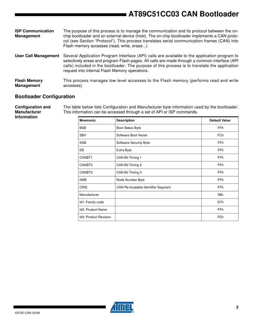
Boot Process The bootloader can be activated in two ways:
• Hardware conditions
• Regular boot process
Hardware Conditions The Hardware conditions (EA = 1, PSEN = 0) during the RESET# falling edge force the on-chip
bootloader execution. In this way the bootloader can be carried out whatever the user Flash
memory content.
As PSEN is an output port in normal operating mode (running user application or bootloader
code) after reset, it is recommended to release PSEN after falling edge of reset signal. The hard-
ware conditions are sampled at reset signal falling edge, thus they can be released at any time
when reset input is low.
7
4251B–CAN–03/08
AT89C51CC03 CAN Bootloader
Regular Boot Process
RESET
BLJB = 1
HardwareCondition
Start Bootloader
FCO N = 00h
SBV < F8h
Start User BootloaderStart Application
Yes
No
Yes
Yes
No
No
Ha
rdw
are
Bo
ot
Pro
ce
ss
So
ftw
are
Bo
ot
Pro
ce
ss
bit ENBOO T in AUXR1 Register isinitia lized with BLJB inverted
ENBOO T = 1PC = F800hFCO N = 0Fh
ENBO OT = 0PC = 0000h
ENBOOT = 1PC = F800hFCON = 00hYes
No

8
4251B–CAN–03/08
AT89C51CC03 CAN Bootloader
Physical Layer The CAN is used to transmit information has the following configuration:
• Standard Frame CAN format 2.0A (identifier 11-bit)
• Frame: Data Frame
• Baud rate: autobaud is performed by the bootloader
CAN Controller
Initialization
Two ways are possible to initialize the CAN controller:
• Use the software autobaud
• Use the user configuration stored in the CANBT1, CANBT2 and CANBT3
The selection between these two solutions is made with EB:
• EB = FFh: the autobaud is performed.
• EB not equal to FFh: the CANBT1:2:3 are used.
CANBT1:3 and EB can be modified by user through a set of API or with ISP commands.
The figure below describes the CAN controller flow.
Figure 2. CAN Controller Initialization
CAN controllerInitialization
EB = FFh
Read CANBT1 valueRead CANBT2 valueRead CANBT3 value
CANBTx = FFhx=(1,3)
CAN Error
CAN macroInitialized
Yes
No
No
No
Yes
Yes
Configure the CANcontroller
Autobaud ok
Set the CAN controller inautobaud mode
Yes
No

9
4251B–CAN–03/08
AT89C51CC03 CAN Bootloader
CAN Autobaud The table below shows the autobaud performance for a point to point connection in X1 mode.
Note: ‘–’ indicates an impossible configuration.
CAN Autobaud
Limitation
The CAN autobaud implemented in the bootloader is efficient only in point-to-point connection.
Because in a point to point connection, the transmit CAN message is repeated until a hardware
acknowledge is done by the receiver.
The bootloader can acknowledge an in-coming CAN frame only if a configuration is found.
This functionality is not guaranteed on a network with several CAN nodes.
8 MHz
11.059
MHz 12 MHz 16 MHz 20 MHz
22.1184
MHz 24 MHz 25 MHz 32 MHz 40 MHz
20 k
100 k
125 k –
250 k –
500 k
1 M – – –
10
4251B–CAN–03/08
AT89C51CC03 CAN Bootloader
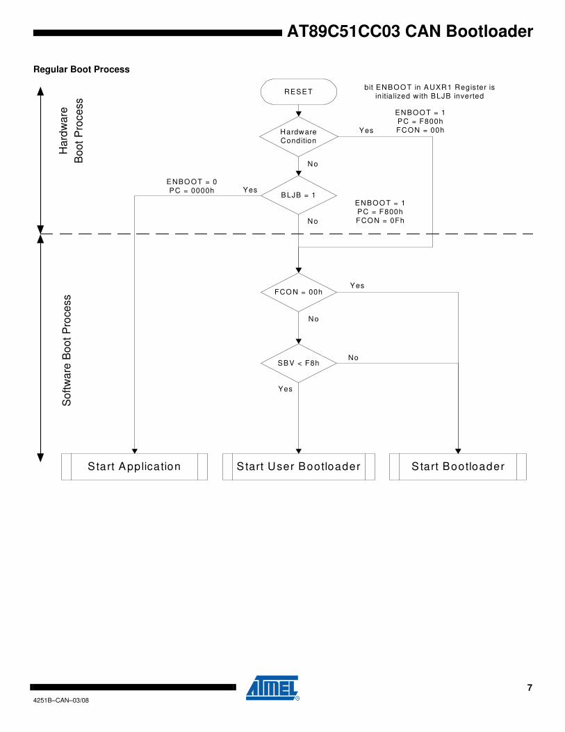
Protocol
Generic CAN Frame
Description
• Identifier: Identifier identifies the frame (or message). Only the standard mode (11-bit) is used.
• Control: Control contains the DLC information (number of data in Data field) 4-bit.
• Data: Data field consists of zero to eight bytes. The interpretation within the frame depends on the
Identifier field.
The CAN protocol manages directly using hardware a checksum and an acknowledge.
Note: To describe the ISP CAN Protocol, we use Symbolic name for Identifier, but default values are
given.
Command Description This protocol allows to:
• Initiate the communication
• Program the Flash or EEPROM Data
• Read the Flash or EEPROM Data
• Program Configuration Information
• Read Configuration and Manufacturer Information
• Erase the Flash
• Start the application
Overview of the protocol is detailed in APPENDIX-1.
Several CAN message identifiers are defined to manage this protocol.
It is possible to allocate a new value for CAN ISP identifiers by writing the byte CRIS with the
base value for the group of identifier.
The maximum value for CRIS is 7Fh and the default CRIS value is 00h.
Identifier Control Data11-bit 1 byte 8 bytes max
Identifier Command Effect Value
ID_SELECT_NODE Open/Close a communication with a node [CRIS]0h
ID_PROG_START Start a Flash/EEPROM programming [CRIS]1h
ID_PROG_DATA Data for Flash/EEPROM programming [CRIS]2h
ID_DISPLAY_DATA Display data [CRIS]3h
ID_WRITE_COMMAND Write in XAF, or Hardware Byte [CRIS]4h
ID_READ_COMMAND Read from XAF or Hardware Byte and special data [CRIS]5h
ID_ERROR Error message from bootloader only [CRIS]6h

11
4251B–CAN–03/08
AT89C51CC03 CAN Bootloader
Figure 3. Identifier Remapping
Communication
Initialization
The communication with a device (CAN node) must be opened prior to initiate any ISP
communication.
To open communication with the device, the Host sends a “connecting” CAN message
(Id_select_node) with the node number (NNB) passed in parameter.
If the node number passed is equal to FFh then the CAN bootloader accepts the communication
(Figure 4).
Otherwise the node number passed in parameter must be equal to the local Node Number (Fig-
ure 5).
Figure 4. First Connection
Figure 5. On Network Connection
Before opening a new communication with another device, the current device communication
must be closed with its connecting CAN message (Id_select_node).
CAN Identifiers
000h
7FFh
ID_errorID_read_commandID_write_commandID_display_dataID_prog_dataID_prog_startID_select_node
CAN ISP identifiers
Group of 7CAN messagesUsed to manage CAN ISP
[CRIS]0h
Host
Interface board between PCand CAN network
Node 1
NNB = FFh (default value)
Host
Interface board between PCand CAN network
Node 0
Node 3
Node 1
Node n
NNB = 00h
NNB = 01h
NNB = 03h NNB = n

12
4251B–CAN–03/08
AT89C51CC03 CAN Bootloader
Request From Host
Note: num_node is the NNB (Node Number Byte) to which the Host wants to talk to.T
Answers From
Bootloader
Note: data[0] contains the bootloader version.
If the communication is closed then all the others messages won’t be managed by bootloader.
Flow Description
Example
Identifier Length data[0]
ID_SELECT_NODE 1 num_node
Identifier Length data[0] data[1] Comment
ID_SELECT_NODE 2 boot_version00h Communication close
01h Communication open
Host Bootloader
Id_select_node message
Wait Select Node
Send Bootloader Version
Read Bootloader Version
Send Select Node message
Time-out 10 ms
Wait Select Node
OR
COMMAND ABORTED
COMMAND FINISHEDCOMMAND FINISHED
with node number in parameter
Id_select_node message
node select = FFh
node select = local node number
state com = com open
State com = com open
State com = com closed
and state of communication
HOST Id_select_node
BOOTLOADER Id_select_node
identifier length data
01 FF
02 01 01
13
4251B–CAN–03/08
AT89C51CC03 CAN Bootloader
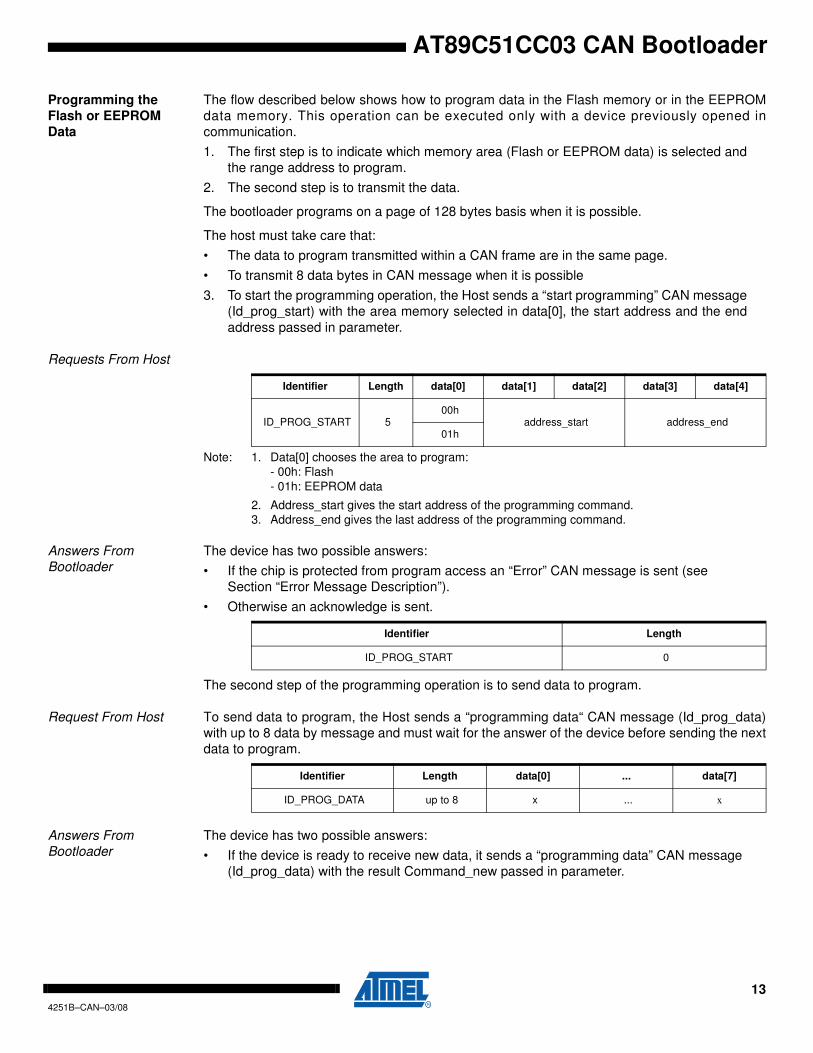
Programming the
Flash or EEPROM
Data
The flow described below shows how to program data in the Flash memory or in the EEPROM
data memory. This operation can be executed only with a device previously opened in
communication.
1. The first step is to indicate which memory area (Flash or EEPROM data) is selected and
the range address to program.
2. The second step is to transmit the data.
The bootloader programs on a page of 128 bytes basis when it is possible.
The host must take care that:
• The data to program transmitted within a CAN frame are in the same page.
• To transmit 8 data bytes in CAN message when it is possible
3. To start the programming operation, the Host sends a “start programming” CAN message
(Id_prog_start) with the area memory selected in data[0], the start address and the end
address passed in parameter.
Requests From Host
Note: 1. Data[0] chooses the area to program: - 00h: Flash - 01h: EEPROM data
2. Address_start gives the start address of the programming command.
3. Address_end gives the last address of the programming command.
Answers From
Bootloader
The device has two possible answers:
• If the chip is protected from program access an “Error” CAN message is sent (see
Section “Error Message Description”).
• Otherwise an acknowledge is sent.
The second step of the programming operation is to send data to program.
Request From Host To send data to program, the Host sends a “programming data“ CAN message (Id_prog_data)
with up to 8 data by message and must wait for the answer of the device before sending the next
data to program.
Answers From
Bootloader
The device has two possible answers:
• If the device is ready to receive new data, it sends a “programming data” CAN message
(Id_prog_data) with the result Command_new passed in parameter.
Identifier Length data[0] data[1] data[2] data[3] data[4]
ID_PROG_START 500h
address_start address_end01h
Identifier Length
ID_PROG_START 0
Identifier Length data[0] ... data[7]
ID_PROG_DATA up to 8 x ... x

14
4251B–CAN–03/08
AT89C51CC03 CAN Bootloader
• If the device has finished the programming, it sends a “programming data” CAN message
(Id_prog_data) with the result Command_ok passed in parameter.
Flow Description
Identifier Length data[0] Description
ID_PROG_DATA 1
00h Command ok
01h Command fail
02h Command new data
Host Bootloader
Id_prog_start message
Id_error message
Id_prog_data message
Id_prog_data message
Column Latch Full
All bytes received
Wait Prog start
SSB = Level 0
Send COMMAND_OK
Wait Data prog
Wait Programming
All bytes received
Send ERROR
Send COMMAND_NEW_DATA
Id_prog_data message
Send prog_start messagewith addresses
Wait ERROR
Send prog_data messagewith 8 datas
Wait COMMAND_N
Wait COMMAND_OK
Wait ProgStart
OR
OR
COMMAND ABORTED
COMMAND FINISHED COMMAND FINISHED
Send ProgStartId_prog_start message

15
4251B–CAN–03/08
AT89C51CC03 CAN Bootloader
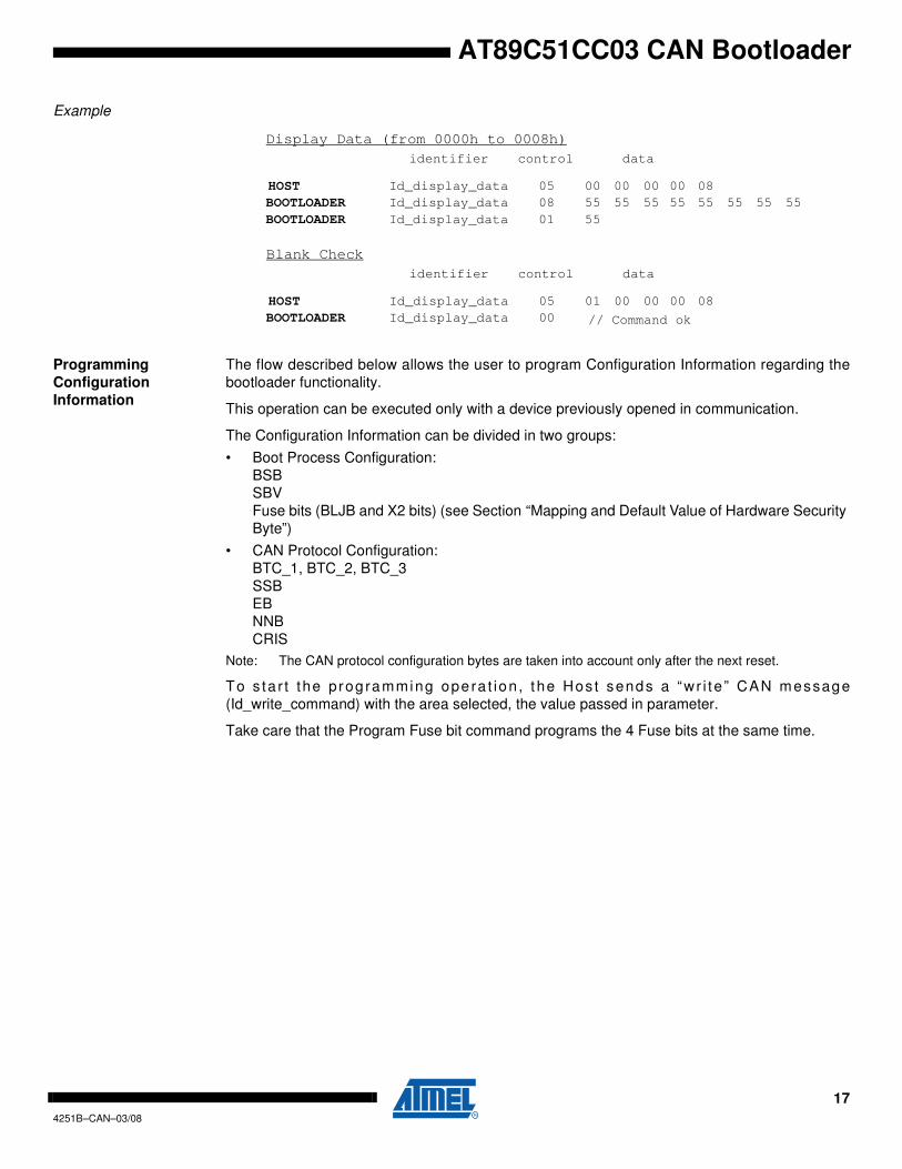
Example
Reading the Flash or
EEPROM Data
The flow described below allows the user to read data in the Flash memory or in the EEPROM
data memory. A blank check command on the Flash memory is possible with this flow.
This operation can be executed only with a device previously opened in communication.
To start the reading operation, the Host sends a “Display Data” CAN message (Id_display_data)
with the area memory selected, the start address and the end address passed in parameter.
The device splits into block of 8 bytes data to transfer to the Host if the number of data to display
is greater than 8 data bytes.
Requests from Host
Note: 1. Data[0] selects the area to read and the operation - 00h: Display Flash - 01h: Blank Check on the Flash - 02h: Display EEPROM data
2. The address_start gives the start address to read.
3. The address_end gives the last address to read.
Answers from
Bootloader
The device has two possible answers:
• If the chip is protected from read access a “Error” CAN message is sent (see Section “Error
Message Description”).
• Otherwise: for a display command the device start to send the data up to 8 by frame to the host. for a
blank check command the device send a result ok or the first address not erased.
Answer to a read command:
HOST Id_prog_start
BOOTLOADER
Id_prog_data
Programming Data (write 55h from 0000h to 0008h in the flash)
identifier control
05 00
08 55
00
55
00
55
data
55 55 55 55
00
55HOST
Id_prog_data 01 02
BOOTLOADER
Id_prog_data 01 55HOST
Id_prog_data 01 00
HOST Id_prog_start
Programming Data (write 55h from 0000h to 0008h in the flash), with SSB in write security
identifier control
04 00 00 00
data
08BOOTLOADER Id_error 01 00
// command_new_data
// command_ok
// error_security
BOOTLOADER Id_prog_start 00
08
Identifier Length data[0] data[1] data[2] data[3] data[4]
ID_DISPLAY_DATA 5
00h
address_start address_end01h
02h
Identifier Length data[n]
ID_DISPLAY_DATA n x

16
4251B–CAN–03/08
AT89C51CC03 CAN Bootloader
Answer to a blank check command:
Flow Description
Identifier Length data[0] data[1] Description
ID_DISPLAY_DATA0 - - Blank Check OK
2 address_start
Host Bootloader
Id_display_data message
Id_error message
Id_display_data message
Blank command
Wait Display Data
SSB = Level2
Send COMMAND_OK
Read Data
All data read
Send ERROR
Send DATA Read
Send display_data messagewith addresses or blank check
Wait ERROR
Wait COMMAND_OK
Wait Data Display
OR
OR
COMMAND ABORTED
COMMAND FINISHED
nb max by frame
All data read
Verify memory
Blank Check
COMMAND FINISHED
Send COMMAND_KO
Id_display_data message
Id_display_data message
Wait COMMAND_KO
COMMAND FINISHED
OR
All data read
COMMAND FINISHED
17
4251B–CAN–03/08
AT89C51CC03 CAN Bootloader
Example
Programming
Configuration
Information
The flow described below allows the user to program Configuration Information regarding the
bootloader functionality.
This operation can be executed only with a device previously opened in communication.
The Configuration Information can be divided in two groups:
• Boot Process Configuration: BSB SBV Fuse bits (BLJB and X2 bits) (see Section “Mapping and Default Value of Hardware Security
Byte”)
• CAN Protocol Configuration: BTC_1, BTC_2, BTC_3 SSB EB NNB CRIS
Note: The CAN protocol configuration bytes are taken into account only after the next reset.
To s ta r t the prog ramming ope ra t ion , t he Hos t sends a “wr i t e ” CAN message
(Id_write_command) with the area selected, the value passed in parameter.
Take care that the Program Fuse bit command programs the 4 Fuse bits at the same time.
HOST Id_display_data
BOOTLOADER Id_display_data
Display Data (from 0000h to 0008h)
identifier control
05 00
08 55
00
55
00
55
data
55 55 55 55
00
55
HOST Id_display_data
BOOTLOADER Id_display_data
Blank Check
identifier control
05 01
00
00 00
data
00
08
08
// Command ok
BOOTLOADER Id_display_data 01 55

18
4251B–CAN–03/08
AT89C51CC03 CAN Bootloader
Requests From Host
Answers From
Bootloader
The device has two possible answers:
• If the chip is protected from program access a “Error” CAN message is sent (see
Section “Error Message Description”).
• Otherwise an acknowledge “Command ok“ is sent.
Flow Description
Identifier Length data[0] data[1] data[2] Description
ID_WRITE_COMMAND3 01h
00h
value
write value in BSB
01h write value in SBV
05h write value in SSB
06h write value in EB
1Ch write value in BTC_1
1Dh write value in BTC_2
1Eh write value in BTC_3
1Fh write value in NNB
20h write value in CRIS
3 02h 00h value write value in Fuse bits
Identifier Length data[0] Description
ID_WRITE_COMMAND 1 00h Command ok
Host Bootloader
Id_write_com message
Id_error message
Wait Write_Command
NO_SECURITY
Send COMMAND_OK
Write Data
Send ERROR_SECURITY
Send Write_Command
Wait ERROR_SECURITY
Wait COMMAND_OK
OR
COMMAND ABORTED
COMMAND FINISHED
Id_write_com message
COMMAND FINISHED

19
4251B–CAN–03/08
AT89C51CC03 CAN Bootloader
Example
Reading Configuration
Information or
Manufacturer
Information
The flow described below allows the user to read the configuration or manufacturer information.
This operation can be executed only with a device previously opened in communication.
To start the reading operation, the Host sends a “Read command” CAN message
(Id_read_command) with the information selected passed in data field.
Requests From Host
00
HOST Id_write_command
BOOTLOADER Id_write_command
identifier control
03 01
01
00 88
data
// command_ok
00
HOST Id_write_command
BOOTLOADER Id_write_command
Write Fuse bit at Fxh
identifier control
02 02
01
F0
data
// command_ok
Write BSB at 88h
Identifier Length data[0] data[1] Description
ID_READ_COMMAND
2 00h
00h Read Bootloader version
01h Read Device ID1
02h Read Device ID2
2 01h
00h Read BSB
01h Read SBV
05h Read SSB
06h Read EB
1Ch Read BTC_1
1Dh Read BTC_2
1Eh Read BTC_3
1Fh Read NNB
20h Read CRIS
30h Read Manufacturer Code
31h Read Family Code
60h Read Product Name
61h Read Product Revision
2 02h 00h Read HSB (Fuse bits)

20
4251B–CAN–03/08
AT89C51CC03 CAN Bootloader
Answers From
Bootloader
The device has two possible answers:
• If the chip is protected from read access an “Error” CAN message is sent (see Section “Error
Message Description”).
• Otherwise: the device answers with a Read Answer CAN message (Id_read_command).
Flow Description
Example
Identifier Length data[n]
ID_READ_COMMAND 1 value
Host Bootloader
Id_read_com message
Id_error message
Wait Read_Com
Send Data read
Read Data
Send ERROR_SECURITY
Send read_com message
Wait ERROR_SECURITY
Wait Value of data
OR
COMMAND ABORTED
COMMAND FINISHED
Id_read_com message
COMMAND FINISHED
RD_WR_SECURITY
HOST Id_read_command
BOOTLOADER Id_read_command
Read Bootloader Version
identifier control
02 00
01
F5
00
data
HOST Id_read_command
BOOTLOADER Id_read_command
Read SBV
identifier control
02 01
01
01
data
// SBV = F5h
55 // Bootloader version 55h
F0
HOST Id_read_command
BOOTLOADER Id_read_command
Read Fuse bit
identifier control
01 02
01
data
// Fuse bit = F0h

21
4251B–CAN–03/08
AT89C51CC03 CAN Bootloader
Erasing the Flash The flow described below allows the user to erase the Flash memory.
This operation can be executed only with a device previously opened in communication.
Two modes of Flash erasing are possible:
• Full Chip erase
• Block erase
The Full Chip erase command erases the whole Flash (64 Kbytes) and sets some Configuration
Bytes at their default values:
• BSB = FFh
• SBV = FFh
• SSB = FFh (NO_SECURITY)
The Block erase command erases only a part of the Flash.
Three Blocks are defined in the AT89C51CC03:
• block0 (From 0000h to 1FFFh)
• block1 (From 2000h to 3FFFh)
• block2 (From 4000h to 7FFFh)
• block3 (From 8000h to BFFFh)
• block4 (From C000h to FFFFh)
•
To start the erasing operation, the Host sends a “write” CAN message (Id_write_command).
Requests From Host
Answers From
Bootloader
As the Program Configuration Information flows, the erase block command has two possible
answers:
• If the chip is protected from program access an “Error” CAN message is sent (see
Section “Error Message Description”).
• Otherwise an acknowledge is sent.
The full chip erase is always executed whatever the Software Security Byte value is.
On a full chip erase command an acknowledge “command ok” is sent.
Identifier Length data[0] data[1] Description
ID_WRITE_COMMAND 2 00h
00h Erase block0 (0k to 8k)
20h Erase block1 (8k to 16k)
40h Erase block2 (16k to 32k)
80h Erase block3 (32k to 48k)
C0h Erase block4 (48k to 64k)
FFh Full chip erase
Identifier Length data[0] Description
ID_WRITE_COMMAND 1 00h Command ok

22
4251B–CAN–03/08
AT89C51CC03 CAN Bootloader
Example
Starting the
Application
The flow described below allows to start the application directly from the bootloader upon a spe-
cific command reception.
This operation can be executed only with a device previously opened in communication.
Two options are possible:
• Start the application with a reset pulse generation (using watchdog). When the device receives this command the watchdog is enabled and the bootloader enters
a waiting loop until the watchdog resets the device. Take care that if an external reset chip is used the reset pulse in output may be wrong and in
this case the reset sequence is not correctly executed.
• Start the application without reset A jump at the address 0000h is used to start the application without reset.
To start the application, the Host sends a “start application” CAN message (Id_write_command)
with the corresponding option passed in parameter.
Requests From Host
Answer From
Bootloader
No answer is returned by the device.
Example
Error Message
Description
The error message is implemented to report when an action required is not possible.
• At the moment only the security error is implemented and only the device can answer this
kind of CAN message (Id_error).
HOST Id_write_command
BOOTLOADER Id_write_command
Full Chip Erase
identifier control
02 00
01
FF
data
00 // command_ok
Identifier Length data[0] data[1] data[2] data[3] Description
ID_WRITE_COMMAND
2
03h
00h - -Start Application with a reset pulse
generation
4 01h addressStart Application with a jump at
“address”
HOST Id_write_command
BOOTLOADER
Start application
identifier control
04 03 01 00 00
data
No answer
Identifier Length data[0] Description
ID_ERROR 1 00h Software Security Error
23
4251B–CAN–03/08
AT89C51CC03 CAN Bootloader
In-Application
Programming/S
elf
Programming
The IAP allows to reprogram a microcontroller on-chip Flash memory without removing it from
the system and while the embedded application is running.
The user application can call Application Programming Interface (API) routines allowing IAP.
These API are executed by the bootloader.
To call the corresponding API, the user must use a set of Flash_api routines which can be linked
with the application.
Example of Flash_api routines are available on the Atmel web site on the software package:
C Flash Drivers for the AT89C51CC03CA for Keil Compilers
The flash_api routines on the package work only with the CAN bootloader.
The flash_api routines are listed in APPENDIX-2.
API Call
Process The application selects an API by setting the 4 variables available when the flash_api library is
linked to the application.
These four variables are located in RAM at fixed address:
• api_command: 1Ch
• api_value: 1Dh
• api_dph: 1Eh
• api_dpl: 1Fh
All calls are made through a common interface “USER_CALL” at the address FFC0h.
The jump at the USER_CALL must be done by LCALL instruction to be able to comeback in the
application.
Before jump at the USER_CALL, the bit ENBOOT in AUXR1 register must be set.
Constraints The interrupts are not disabled by the bootloader.
Interrupts must be disabled by user prior to jump to the USER_CALL, then re-enabled when
returning.
Interrupts must also be disabled before accessing EEPROM Data then re-enabled after.
The user must take care of hardware watchdog before launching a Flash operation.
For more information regarding the Flash writing time see the AT89C51CC03 datasheet.

24
4251B–CAN–03/08
AT89C51CC03 CAN Bootloader
API Commands Several types of APIs are available:
• Read/Program Flash and EEPROM Data memory
• Read Configuration and Manufacturer Information
• Program Configuration Information
• Erase Flash
• Start bootloader
Read/Program Flash
and EEPROM Data
Memory
All routines to access EEPROM Data are managed directly from the application without using
bootloader resources.
To read the Flash memory the bootloader is not involved.
For more details on these routines see the AT89C51CC03 Datasheet sections “Program/Code
Memory” and “EEPROM Data Memory”
Two routines are available to program the Flash:
– __api_wr_code_byte
– __api_wr_code_page
• The application program load the column latches of the Flash then call the
__api_wr_code_byte or __api_wr_code_page see datasheet in section “Program/Code
Memory”.
• Parameter settings
• instruction: LCALL FFC0h.
Note: No special resources are used by the bootloader during this operation
Read Configuration
and Manufacturer
Information
• Parameter settings
API Name api_command api_dph api_dpl api_value
__api_wr_code_byte
__api_wr_code_page0Dh - - -
API Name api_command api_dph api_dpl api_value
__api_rd_HSB 08h - 00h return HSB
__api_rd_BSB 05h - 00h return BSB
__api_rd_SBV 05h - 01h return SBV
__api_rd_SSB 05h - 05h return SSB
__api_rd_EB 05h - 06h return EB
__api_rd_CANBTC1 05h - 1Ch return CANBTC1
__api_rd_CANBTC2 05h - 1Dh return CANBTC2
__api_rd_CANBTC3 05h - 1Eh return CANBTC3
__api_rd_NNB 05h - 1Fh return NNB
__api_rd_CRIS 05h - 20h return CRIS
__api_rd_manufacturer 05h - 30hreturn
manufacturer id
__api_rd_device_id1 05h - 31h return id1

25
4251B–CAN–03/08
AT89C51CC03 CAN Bootloader
• Instruction: LCALL FFC0h.
• At the complete API execution by the bootloader, the value to read is in the api_value
variable.
Note: No special resources are used by the bootloader during this operation
Program
Configuration
Information
• Parameter settings
• instruction: LCALL FFC0h.
Note: 1. See in the AT89C51CC03 datasheet the time that a write operation takes.
2. No special resources are used by the bootloader during these operations
Erasing the Flash The AT89C51CC03 Flash memory is divided in several blocks:
Block 0: from address 0000h to 1FFFh
Block 1: from address 2000h to 3FFFh
Block 2: from address 4000h to 7FFFh
Block 3: from address 8000h to BFFFh
Block 4: from address C000h to FFFFh
These five blocks contain 256 pages.
__api_rd_device_id2 05h - 60h return id2
__api_rd_device_id3 05h - 61h return id3
__api_rd_bootloader_version 0Eh - 00h return value
API Name api_command api_dph api_dpl api_value
API Name api_command api_dph api_dpl api_value
__api_clr_BLJB 07h - -(HSB & BFh) |
40h
__api_set_BLJB 07h - - HSB & BFh
__api_clr_X2 07h - -(HSB & 7Fh) |
80h
__api_set_X2 07h - - HSB & 7Fh
__api_wr_BSB 04h - 00h value to write
__api_wr_SBV 04h - 01h value to write
__api_wr_SSB 04h - 05h value to write
__api_wr_EB 04h - 06h value to write
__api_wr_CANBTC1 04h - 1Ch value to write
__api_wr_CANBTC2 04h - 1Dh value to write
__api_wr_CANBTC3 04h - 1Eh value to write
__api_wr_NNB 04h - 1Fh value to write
__api_wr_CRIS 04h - 20h value to write

26
4251B–CAN–03/08
AT89C51CC03 CAN Bootloader
• Parameter settings
• instruction: LCALL FFC0h.
Note: 1. See the AT89C51CC03 datasheet for the time that a write operation takes and this time must
multiply by the number of pages.
2. No special resources are used by the bootloader during these operations
Starting the
Bootloader
There are two start bootloader routines possible:
This routine allows to start at the beginning of the bootloader as after a reset. After calling this
routine the regular boot process is performed and the communication must be opened before
any action.
• No special parameter setting
• Set bit ENBOOT in AUXR1 register
• instruction: LJUMP or LCALL at address F800h
This routine allows to start the bootloader with the CAN bit configuration of the application and
start with the state "communication open". That means the bootloader will return the message
“id_select_node” with the field com port open.
• No special parameter setting
• Set bit ENBOOT in AUXR1 register
• instruction: LJUMP or LCALL at address FF00h
API Name api_command api_dph api_dpl api_value
__api_erase_block0 00h 00h - -
__api_erase_block1 00h 20h -
__api_erase_block2 00h 40h -
__api_erase_block3 00h 80h - -
__api_erase_block4 00h C0h -
27
4251B–CAN–03/08
AT89C51CC03 CAN Bootloader
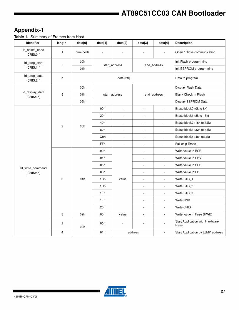
Appendix-1Table 1. Summary of Frames from Host
Identifier length data[0] data[1] data[2] data[3] data[4] Description
Id_select_node
(CRIS:0h)1 num node - - - - Open / Close communication
Id_prog_start
(CRIS:1h)5
00hstart_address end_address
Init Flash programming
01h Init EEPROM programming
Id_prog_data
(CRIS:2h)n data[0:8] Data to program
Id_display_data
(CRIS:3h)5
00h
start_address end_address
Display Flash Data
01h Blank Check in Flash
02h Display EEPROM Data
Id_write_command
(CRIS:4h)
2 00h
00h - - - Erase block0 (0k to 8k)
20h - - - Erase block1 (8k to 16k)
40h - - - Erase block2 (16k to 32k)
80h - - - Erase block3 (32k to 48k)
C0h - - - Erase block4 (48k to64k)
FFh - - - Full chip Erase
3 01h
00h
value
- - Write value in BSB
01h - - Write value in SBV
05h - - Write value in SSB
06h - - Write value in EB
1Ch - - Write BTC_1
1Dh - - Write BTC_2
1Eh - - Write BTC_3
1Fh - - Write NNB
20h - - Write CRIS
3 02h 00h value - - Write value in Fuse (HWB)
203h
00h - - -Start Application with Hardware
Reset
4 01h address - Start Application by LJMP address

28
4251B–CAN–03/08
AT89C51CC03 CAN Bootloader
Id_read_command
(CRIS:5h)
2 00h
00h - - - Read Bootloader Version
01h - - - Read Device ID1
02h - - - Read Device ID2
2 01h
00h - - - Read BSB
01h - - - Read SBV
05h - - - Read SSB
06h - - - Read EB
30h - - - Read Manufacturer Code
31h - - - Read Family Code
60h - - - Read Product Name
61h - - - Read Product Revision
1Ch - - - Read BTC_1
1Dh - - - Read BTC_2
1Eh - - - Read BTC_3
1Fh - - - Read NNB
20h - - - Read CRIS
2 02h 00h - - - Read HSB
Table 1. Summary of Frames from Host (Continued)
Identifier length data[0] data[1] data[2] data[3] data[4] Description
Table 2. Summary of Frames from Target (Bootloader)
Identifier length data[0] data[1] data[2] data[3] data[4] Description
Id_select_node
(CRIS:0h)2
Boot
version
00h - - - communication close
01h - - - communication open
Id_prog_start
(CIRS:1h)0 - - - - - Command ok
Id_prog_data
(CRIS:2h)1
00h - - - - Command ok
01h - - - - Command fail
02h - - - - Command New Data
Id_display_data
(CRIS:3h)
n n data (n = 0 to 8) Data read
0 - - - - - Blank Check ok
2 first address not blank - - - Blank Check fail
Id_write_command
(CIRS:4h)1 00h - - - - Command ok
Id_read_command
(CRIS:5h)1 Value - - - Read Value

29
4251B–CAN–03/08
AT89C51CC03 CAN Bootloader
Id_error
(CRIS:6h)1 00h - - - - Software Security Error
Table 2. Summary of Frames from Target (Bootloader) (Continued)
Identifier length data[0] data[1] data[2] data[3] data[4] Description

30
4251B–CAN–03/08
AT89C51CC03 CAN Bootloader
Appendix-2Table 3. API Summary
Function Name
Bootloader
Execution api_command api_dph api_dpl api_value
__api_rd_code_byte no
__api_wr_code_byte yes 0Dh - - -
__api_wr_code_page yes 0Dh - - -
__api_erase block0 yes 00h 00h - -
__api_erase block1 yes 00h 20h - -
__api_erase block2 yes 00h 40h - -
__api_erase block3 yes 00h 80h - -
__api_erase block4 yes 00h C0h - -
__api_rd_HSB yes 08h - 00h return value
__api_clr_BLJB yes 07h - - (HSB & BFh) | 40h
__api_set_BLJB yes 07h - - HSB & BFh
__api_clr_X2 yes 07h - - (HSB & 7Fh) | 80h
__api_set_X2 yes 07h - - HSB & 7Fh
__api_rd_BSB yes 05h - 00h return value
__api_wr_BSB yes 04h - 00h value
__api_rd_SBV yes 05h - 01h return value
__api_wr_SBV yes 04h - 01h value
__api_erase_SBV yes 04h - 01h FFh
__api_rd_SSB yes 05h - 05h return value
__api_wr_SSB yes 04h - 05h value
__api_rd_EB yes 05h - 06h return value
__api_wr_EB yes 04h - 06h value
__api_rd_CANBTC1 yes 05h - 1Ch return value
__api_wr_CANBTC1 yes 04h - 1Ch value
__api_rd_CANBTC2 yes 05h - 1Dh return value
__api_wr_CANBTC2 yes 04h - 1Dh value
__api_rd_CANBTC3 yes 05h - 1Eh return value
__api_wr_CANBTC3 yes 04h - 1Eh value
__api_rd_NNB yes 05h - 1Fh return value
__api_wr_NNB yes 04h - 1Fh value
__api_rd_CRIS yes 05h - 20h return value
__api_wr_CRIS yes 04h - 20h value

31
4251B–CAN–03/08
AT89C51CC03 CAN Bootloader
__api_rd_manufacturer yes 05h - 30h return value
__api_rd_device_id1 yes 05h - 31h return value
__api_rd_device_id2 yes 05h - 60h return value
__api_rd_device_id3 yes 05h - 61h return value
__api_rd_bootloader_version yes 0Eh - 00h return value
__api_eeprom_busy no - - - -
__api_rd_eeprom_byte no - - - -
__api_wr_eeprom_byte no - - - -
__api_start_bootloader no - - - -
__api_start_isp no - - - -
Table 3. API Summary
Function Name
Bootloader
Execution api_command api_dph api_dpl api_value

4251B–CAN–03/08
Headquarters International
Atmel Corporation
2325 Orchard Parkway
San Jose, CA 95131
USA
Tel: 1(408) 441-0311
Fax: 1(408) 487-2600
Atmel Asia
Room 1219
Chinachem Golden Plaza
77 Mody Road Tsimshatsui
East Kowloon
Hong Kong
Tel: (852) 2721-9778
Fax: (852) 2722-1369
Atmel Europe
Le Krebs
8, Rue Jean-Pierre Timbaud
BP 309
78054 Saint-Quentin-en-
Yvelines Cedex
France
Tel: (33) 1-30-60-70-00
Fax: (33) 1-30-60-71-11
Atmel Japan
9F, Tonetsu Shinkawa Bldg.
1-24-8 Shinkawa
Chuo-ku, Tokyo 104-0033
Japan
Tel: (81) 3-3523-3551
Fax: (81) 3-3523-7581
Product Contact
Web Site
www.atmel.com
Technical Support
Enter Product Line E-mail
Sales Contact
www.atmel.com/contacts
Literature Requests
www.atmel.com/literature
Disclaimer: The information in this document is provided in connection with Atmel products. No license, express or implied, by estoppel or otherwise, to any intellectual property right is granted by this document or in connection with the sale of Atmel products. EXCEPT AS SET FORTH IN ATMEL’S TERMS AND CONDI-TIONS OF SALE LOCATED ON ATMEL’S WEB SITE, ATMEL ASSUMES NO LIABILITY WHATSOEVER AND DISCLAIMS ANY EXPRESS, IMPLIED OR STATUTORY WARRANTY RELATING TO ITS PRODUCTS INCLUDING, BUT NOT LIMITED TO, THE IMPLIED WARRANTY OF MERCHANTABILITY, FITNESS FOR A PARTICULAR PURPOSE, OR NON-INFRINGEMENT. IN NO EVENT SHALL ATMEL BE LIABLE FOR ANY DIRECT, INDIRECT, CONSEQUENTIAL, PUNITIVE, SPECIAL OR INCIDEN-TAL DAMAGES (INCLUDING, WITHOUT LIMITATION, DAMAGES FOR LOSS OF PROFITS, BUSINESS INTERRUPTION, OR LOSS OF INFORMATION) ARISING OUT OF THE USE OR INABILITY TO USE THIS DOCUMENT, EVEN IF ATMEL HAS BEEN ADVISED OF THE POSSIBILITY OF SUCH DAMAGES. Atmel makes no representations or warranties with respect to the accuracy or completeness of the contents of this document and reserves the right to make changes to specifications and product descriptions at any time without notice. Atmel does not make any commitment to update the information contained herein. Unless specifically provided otherwise, Atmel products are not suitable for, and shall not be used in, automotive applications. Atmel’s products are not intended, authorized, or warranted for use as components in applications intended to support or sustain life.
© 2008 Atmel Corporation. All rights reserved. Atmel®, logo and combinations thereof, and others are registered trademarks or trademarks of
Atmel Corporation or its subsidiaries. Other terms and product names may be trademarks of others.