Embed Size (px)
Citation preview
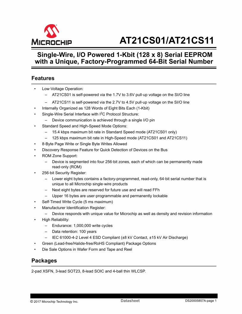
AT21CS01AT21CS11 Single-Wire IO Powered 1-Kbit (128 x 8) Serial EEPROMwith a Unique Factory-Programmed 64-Bit Serial Number
Features
bull Low‑Voltage Operationndash AT21CS01 is self-powered via the 17V to 36V pull‑up voltage on the SIO line
ndash AT21CS11 is self-powered via the 27V to 45V pull‑up voltage on the SIO linebull Internally Organized as 128 Words of Eight Bits Each (1-Kbit)bull Single-Wire Serial Interface with I2C Protocol Structure
ndash Device communication is achieved through a single IO pinbull Standard Speed and High-Speed Mode Options
ndash 154 kbps maximum bit rate in Standard Speed mode (AT21CS01 only)ndash 125 kbps maximum bit rate in High-Speed mode (AT21CS01 and AT21CS11)
bull 8‑Byte Page Write or Single Byte Writes Allowedbull Discovery Response Feature for Quick Detection of Devices on the Busbull ROM Zone Support
ndash Device is segmented into four 256‑bit zones each of which can be permanently maderead‑only (ROM)
bull 256‑bit Security Registerndash Lower eight bytes contains a factory-programmed read-only 64‑bit serial number that is
unique to all Microchip single‑wire productsndash Next eight bytes are reserved for future use and will read FFhndash Upper 16 bytes are user‑programmable and permanently lockable
bull Self‑Timed Write Cycle (5 ms maximum)bull Manufacturer Identification Register
ndash Device responds with unique value for Microchip as well as density and revision informationbull High Reliability
ndash Endurance 1000000 write cyclesndash Data retention 100 yearsndash IEC 61000-4-2 Level 4 ESD Compliant (plusmn8 kV Contact plusmn15 kV Air Discharge)
bull Green (Lead-freeHalide-freeRoHS Compliant) Package Optionsbull Die Sale Options in Wafer Form and Tape and Reel
Packages
2-pad XSFN 3-lead SOT23 8-lead SOIC and 4-ball thin WLCSP
copy 2017 Microchip Technology Inc Datasheet DS20005857A-page 1
Package Types (not to scale)
8-lead SOIC(Top View)
NC 1
2
3
4
8
7
6
5
NC
NC
GND
NC
NC
NC
SIO
SIO
GND
4-ball WLCSP(Top View)
NC
NC
A1 A2
B1 B2
3
2
1
GND
SIO
NC
3-lead SOT23(Top View)
SIO
GND
1
2
2-pad XSFN(Top View)
Description
The AT21CS0111 is a 2-pin memory (SIO signal and Ground) that harvests energy from the signal pin topower the integrated circuit It provides 1024 bits of Serial Electrically Erasable and Programmable Read-Only Memory (SEEPROM) organized as 128 words of eight bits each
The device is optimized to add configuration and use information in unpowered attachments using a two-pointmechanical connection that brings only one signal (SIO) and GND to the unpowered attachment Someunpowered attachment application examples include analog sensor calibration data storage ink and tonerprinter cartridge identification and management of after‑market consumables The devicersquos softwareaddressing scheme allows up to eight devices to share a common single‑wire bus The device is available inspace‑saving package options and operates with an external pull‑up voltage from 17V to 36V on the SIOline (AT21CS01) or from 27V to 45V on the SIO line (AT21CS11)
AT21CS01AT21CS11
copy 2017 Microchip Technology Inc Datasheet DS20005857A-page 2
System Configuration Using Single-Wire Serial EEPROMs
Bus MasterMicrocontroller
Slave 0AT21CSXX
GND
VCC
GND
SIO
RPUP
(See Sections 13 and 14 for requirements)
VPUP
SIO
Slave 1AT21CSXX
GND
SIO
Slave 7AT21CSXX
GND
SIO
Block Diagram
1 page
InternalTiming
Generation
GND
MemorySystem Control
Module
High VoltageGeneration Circuit
Data amp ACK InputOutput Control
CommandControl
ResetDetection
DOUT
DIN
Device Configuration
LatchesSIODevice
PowerExtraction
EEPROM Array
Column Decoder
Row
Dec
oder
Data Register
AT21CS01AT21CS11
copy 2017 Microchip Technology Inc Datasheet DS20005857A-page 3
Table of Contents
Features 1
Packages1
Package Types (not to scale) 2
Description2
System Configuration Using Single-Wire Serial EEPROMs3
Block Diagram 3
1 Electrical Characteristics 611 Absolute Maximum Ratings(1) 612 AT21CS0111 DC and AC Operating Range613 AT21CS01 DC Characteristics(1)614 AT21CS11 DC Characteristics(1) 715 AT21CS0111 AC Characteristics8
2 Pin Descriptions1121 No Connect1122 Serial Input and Output11
3 Device Operation and Communication1231 Single-Wire Bus Transactions 12
4 Device Addressing and I2C Protocol Emulation 1841 Memory Organization18
5 Available Opcodes2051 EEPROM Access (Opcode Ah)2052 Security Register Access (Opcode Bh)2053 Lock Security Register (Opcode 2h) 2054 ROM Zone Register Access (Opcode 7h)2055 Freeze ROM Zone State (Opcode 1h) 2156 Manufacturer ID Read (Opcode Ch) 2157 Standard Speed Mode (Opcode Dh)2158 High-Speed Mode (Opcode Eh)21
6 Write Operations2261 Device Behavior During Internal Write Cycle 2262 Byte Write2263 Page Write2364 Writing to the Security Register2365 Locking the Security Register2466 Setting the Device Speed25
AT21CS01AT21CS11
copy 2017 Microchip Technology Inc Datasheet DS20005857A-page 4
7 Read Operations 2771 Current Address Read within the EEPROM2772 Random Read within the EEPROM 2873 Sequential Read within the EEPROM2874 Read Operations in the Security Register2975 Manufacturer ID Read30
8 ROM Zones 3281 ROM Zone Size and ROM Zone Registers3282 Programming and Reading the ROM Zone Registers3283 Device Response to a Write Command Within an Enabled ROM Zone 34
9 Device Default Condition from Microchip 36
10 Packaging Information37101 Package Marking Information37
11 Revision History42
The Microchip Web Site 43
Customer Change Notification Service43
Customer Support 43
Product Identification System44
Microchip Devices Code Protection Feature 45
Legal Notice45
Trademarks 45
Quality Management System Certified by DNV46
Worldwide Sales and Service47
AT21CS01AT21CS11
copy 2017 Microchip Technology Inc Datasheet DS20005857A-page 5
1 Electrical Characteristics
11 Absolute Maximum Ratings(1)
Temperature under bias -55degC to +125degC
Storage temperature -65degC to +150degC
Voltage on any pin with respect to ground -06V to VPUP +05V
DC output current 150 mA
Note 1 Stresses beyond those listed under ldquoAbsolute Maximum Ratingsrdquo may cause permanent damage to
the device This is a stress rating only and functional operation of the device at these or any otherconditions beyond those indicated in the operational sections of this specification are not impliedExposure to absolute maximum rating conditions for extended periods may affect device reliability
12 AT21CS0111 DC and AC Operating Range
AT21CS01 AT21CS11
Operating Temperature (Case) Industrial Temperature Range -40degC to +85degC -40degC to +85degC
VPUP Voltage tied to SIO Voltage Range 17V to 36V 27V to 45V
13 AT21CS01 DC Characteristics(1)
Parameter Symbol Minimum Typical(2) Maximum Units Test Conditions
Pull-up Voltage VPUP 17 mdash 36 V High-Speedmode
27 mdash 36 V Standard Speedmode
Pull-up Resistance RPUP 130 mdash 200 Ω VPUP = 17V
02 mdash 18 kΩ VPUP = 27V
033 mdash 4 kΩ VPUP = 36V
Active Current Read IA1 mdash 008 03 mA VPUP = 36VSIO = VPUP
Active Current Write IA2 mdash 020 05 mA VPUP = 36V
Standby Current ISB mdash 06 15 microA VPUP = 18V(3)SIO = VPUP
mdash 07 25 microA VPUP = 36V
Input Low Level(3)(4) VIL ndash06 mdash 05 V
Input High Level(3)(4) VIH VPUP x 07 mdash VPUP + 05 V
AT21CS01AT21CS11
copy 2017 Microchip Technology Inc Datasheet DS20005857A-page 6
Parameter Symbol Minimum Typical(2) Maximum Units Test Conditions
SIO Hysteresis(3)(4)(5) VHYS 0128 mdash 117 V
Output Low Level VOL 0 mdash 04 V IOL = 4 mA
Bus Capacitance CBUS mdash mdash 1000 pF
Note 1 Parameters are applicable over the operating range in AT21CS0111 DC and AC Operating Range
unless otherwise noted2 Typical values characterized at TA = +25degC unless otherwise noted3 This parameter is characterized but is not 100 tested in production4 VIH VIL and VHYS are a function of the internal supply voltage which is a function of VPUP RPUP
CBUS and timing used Use of a lower VPUP higher RPUP higher CBUS and shorter tRCV createslower VIH VIL and VHYS values
5 Once VIH is crossed on a rising edge of SIO the voltage on SIO must drop at least by VHYS to bedetected as a logic lsquo0rsquo
14 AT21CS11 DC Characteristics(1)
Parameter Symbol Minimum Typical(2) Maximum Units Test Conditions
Pull-up Voltage VPUP 27 mdash 45 V High-Speedmode
Pull-up Resistance RPUP 02 mdash 18 kΩ VPUP = 27V
04 mdash 54 kΩ VPUP = 45V
Active Current Read IA1 mdash 008 03 mA VPUP = 45VSIO = VPUP
Active Current Write IA2 mdash 020 05 mA VPUP = 45V
Standby Current ISB mdash 06 15 microA VPUP = 27V(3)SIO = VPUP
mdash 07 30 microA VPUP = 45VSIO = VPUP
Input Low Level(3)(4) VIL ndash06 mdash 05 V
Input High Level(3)(4) VIH VPUP x 07 mdash VPUP + 05 V
SIO Hysteresis(3)(4)(5) VHYS 0128 mdash 14 V
Output Low Level VOL 0 mdash 04 V IOL = 4 mA
Bus Capacitance CBUS mdash mdash 1000 pF
Note 1 Parameters are applicable over the operating range in AT21CS0111 DC and AC Operating Range
unless otherwise noted2 Typical values characterized at TA = +25degC unless otherwise noted3 This parameter is characterized but is not 100 tested in production
AT21CS01AT21CS11
copy 2017 Microchip Technology Inc Datasheet DS20005857A-page 7
4 VIH VIL and VHYS are a function of the internal supply voltage which is a function of VPUP RPUPCBUS and timing used Use of a lower VPUP higher RPUP higher CBUS and shorter tRCV createslower VIH VIL and VHYS values
5 Once VIH is crossed on a rising edge of SIO the voltage on SIO must drop at least by VHYS to bedetected as a logic lsquo0rsquo
15 AT21CS0111 AC Characteristics
151 Reset and Discovery Response Timing
Parameter and Condition(1)(2) Symbol StandardSpeed(3)(4)
High Speed Units
Min Max Min Max
Reset Low Time Device in InactiveState
tRESET 480 mdash 48 mdash micros
Discharge Low Time Device in ActiveWrite Cycle (tWR)
tDSCHG 150 mdash 150 mdash micros
Reset Recovery Time tRRT NA NA 8 mdash micros
Discovery Response Request tDRR NA NA 1 2 - tPUP(5) micros
Discovery Response AcknowledgeTime
tDACK NA NA 8 24 micros
Master Strobe Discovery ResponseTime
tMSDR NA NA 2 6 micros
SIO High Time for StartStopCondition
tHTSS NA NA 150 mdash micros
Note 1 Parameters applicable over operating range in AT21CS0111 DC and AC Operating Range unless
otherwise noted2 AC measurement conditions for the table above
ndash Loading capacitance on SIO 100 pFndash RPUP (bus line pull-up resistor to VPUP) 1 kΩ VPUP 27V
3 Due to the fact that the device will default to High-Speed mode upon Reset the Reset andDiscovery Response Timing after tRESET does not apply for Standard Speed mode High-Speedmode timing applies in all cases after tRESET
4 Standard Speed is not available on the AT21CS115 tPUP is the time required once the SIO line is released to be pulled up from VIL to VIH This value is
application specific and is a function of the loading capacitance on the SIO line as well as the RPUPchosen Limits for these values are provided in AT21CS01 DC Characteristics(1) and AT21CS11DC Characteristics(1)
AT21CS01AT21CS11
copy 2017 Microchip Technology Inc Datasheet DS20005857A-page 8
152 Data Communication Timing
Parameter and Condition(1)(2) Symbol Frame Type StandardSpeed(3)
High Speed Units
Min Max Min Max
Bit Frame Duration tBIT Input andOutput Bit
Frame
40 100 tLOW0 +tPUP
(4) +tRCV
25 micros
SIO High Time for StartStopCondition
tHTSS Input BitFrame
600 mdash 150 mdash micros
SIO Low Time Logic lsquo0rsquoCondition
tLOW0 Input BitFrame
24 64 6 16 micros
SIO Low Time Logic lsquo1rsquoCondition
tLOW1 Input BitFrame
4 8 1 2 micros
Master SIO Low Time DuringRead
tRD Output BitFrame
4 8 -tPUP
(4)1 2 -
tPUP(4)
micros
Master Read Strobe Time tMRS Output BitFrame
tRD +tPUP
(4)8 tRD +
tPUP(4)
2 micros
Data Output Hold Time (Logiclsquo0rsquo)
tHLD0 Output BitFrame
8 24 2 6 micros
Slave Recovery Time tRCV Input andOutput Bit
Frame
8 mdash 2(5) mdash micros
Noise Filtering Capability onSIO
tNOISE Input BitFrame
05 mdash mdash mdash micros
Note 1 Parameters applicable over operating range in AT21CS0111 DC and AC Operating Range unless
otherwise noted2 AC measurement conditions for the table above
ndash Loading capacitance on SIO 100 pFndash RPUP (bus line pull-up resistor to VPUP) 1 kΩ VPUP 27V
3 Standard Speed is not available on the AT21CS114 tPUP is the time required once the SIO line is released to be pulled up from VIL to VIH This value is
application specific and is a function of the loading capacitance on the SIO line as well as the RPUPchosen Limits for these values are provided in AT21CS01 DC Characteristics(1)
5 The system designer must select an combination of RPUP CBUS and tBIT such that the minimumtRCV is satisfied The relationship of tRCV within the bit frame can be expressed by the followingformula tBIT = tLOW0 + tPUP + tRCV
AT21CS01AT21CS11
copy 2017 Microchip Technology Inc Datasheet DS20005857A-page 9
153 EEPROM Cell Performance Characteristics
Operation Min Max Units Test Condition
Write Cycle Time(tWR)
mdash 5 ms VPUP (min) lt VPUP lt VPUP (max)TA = 25degC Byte or Page Write mode
Write Endurance(1) 1000000 mdash Write Cycles VPUP (min) lt VPUP lt VPUP (max)TA = 25degC Byte or Page Write mode
Data Retention(2) 100 mdash Years VPUP (min) lt VPUP lt VPUP (max)TA = 55degC
Note 1 Write endurance performance is determined through characterization and the qualification process2 The data retention capability is determined through qualification and checked on each device in
production
AT21CS01AT21CS11
copy 2017 Microchip Technology Inc Datasheet DS20005857A-page 10
2 Pin DescriptionsThe descriptions of the pins are listed in Table 2-1
Table 2-1 Pin Function Table
Name 2-pad XSFN 3-lead SOT23 8-lead SOIC 4-ball WLCSP Function
NC mdash mdash 1 mdash No Connect
NC mdash mdash 2 mdash No Connect
NC mdash 2 3 mdash No Connect
GND 2 3 4 B1 Ground
SIO 1 1 5 A1 Serial Input andOutput
NC mdash mdash 6 No Connect
NC mdash mdash 7 mdash No Connect
NC mdash mdash 8 mdash No Connect
21 No ConnectThe NC pins are not internally connected These pins can be connected to GND or left floating
22 Serial Input and OutputThe SIO pin is an open-drain bidirectional inputoutput pin used to serially transfer data to and from thedevice
The SIO pin must be pulled high using an external pull‑up resistor (not to exceed 4 kΩ in value) and maybe wire-ORed with any number of other open‑drain or open‑collector pins from other devices on the samebus
The device also uses the SIO pin as its voltage source by drawing and storing power during the periodsthat the pin is pulled high to a voltage level between 17V and 36V (AT21CS01) and between 27V and45V (AT21CS11)
AT21CS01AT21CS11
copy 2017 Microchip Technology Inc Datasheet DS20005857A-page 11
3 Device Operation and CommunicationThe AT21CS0111 operates as a slave device and utilizes a single‑wire digital serial interface tocommunicate with a host controller commonly referred to as the bus master The master controls all readand write operations to the slave devices on the serial bus The device has two speeds of operationStandard Speed mode (AT21CS01) and High-Speed mode (AT21CS01 and AT21CS11)
The device utilizes an 8-bit data structure Data is transferred to and from the device via the single‑wireserial interface using the Serial InputOutput (SIO) pin Power to the device is also provided via the SIOpin thus only the SIO pin and the GND pin are required for device operation Data sent to the deviceover the single‑wire bus is interpreted by the state of the SIO pin during specific time intervals or slotsEach time slot is referred to as a bit frame and lasts tBIT in duration The master initiates all bit frames bydriving the SIO line low All commands and data information are transferred with the Most Significant bit(MSb) first
The software sequence sent to the device is an emulation of what would be sent to an I2C SerialEEPROM with the exception that typical 4-bit device type identifier of 1010b in the device address isreplaced by a 4-bit opcode The device has been architected in this way to allow for rapid deploymentand significant reuse of existing I2C firmware For more details about the way the device operates referto Device Addressing and I2C Protocol Emulation
During bus communication one data bit is transmitted in every bit frame and after eight bits (one byte) ofdata has been transferred the receiving device must respond with either an acknowledge (ACK) or a no-acknowledge (NACK) response bit during a ninth bit window There are no unused clock cycles duringany read or write operation so there must not be any interruptions or breaks in the data stream duringeach data byte transfer and ACK or NACK clock cycle In the event where an unavoidable systeminterrupt is required refer to the requirements outlined in Communication Interruptions
31 Single-Wire Bus TransactionsTypes of data transmitted over the SIO line
bull Reset and Discovery Responsebull Logic lsquo0rsquo or Acknowledge (ACK)bull Logic lsquo1rsquo or No Acknowledge (NACK)bull Start Conditionbull Stop Condition
The Reset and Discovery Response is not considered to be part of the data stream to the devicewhereas the remaining four transactions are all required in order to send data to and receive data fromthe device The difference between the different types of data stream transactions is the duration thatSIO is driven low within the bit frame
311 Device ResetPower-up and Discovery Response
3111 Resetting the DeviceA Reset and Discovery Response sequence is used by the master to reset the device as well as toperform a general bus call to determine if any devices are present on the bus
To begin the Reset portion of the sequence the master must drive SIO low for a minimum time If thedevice is not currently busy with other operations the master can drive SIO low for a time of tRESET Thelength of tRESET differs for Standard Speed mode and for High-Speed mode
AT21CS01AT21CS11
copy 2017 Microchip Technology Inc Datasheet DS20005857A-page 12
However if the device is busy the master must drive SIO for a longer time of tDSCHG to ensure the deviceis reset as discussed in Interrupting the Device during an Active Operation The Reset time forces anyinternal charge storage within the device to be consumed causing the device to lose all remainingstandby power available internally
Upon SIO being released for a sufficient amount of time to allow the device time to power-up andinitialize the master must then always request a Discovery Response Acknowledge from theAT21CS0111 prior to any commands being sent to the device The master can then determine if anAT21CS0111 is present by sampling for the Discovery Response Acknowledge from the device
3112 Device Response Upon Reset or Power-UpAfter the device has been powered up or after the master has reset the device by holding the SIO linelow for tRESET or tDSCHG the master must then release the line which will be pulled high by an externalpull-up resistor The master must then wait an additional minimum time of tRRT before the master canrequest a Discovery Response Acknowledge from the device
The Discovery Response Acknowledge sequence begins by the master driving the SIO line low whichwill start the AT21CS0111 internal timing circuits The master must continue to drive the line low for tDRR
During the tDRR time the AT21CS0111 will respond by concurrently driving SIO low The device willcontinue to drive SIO low for a total time of tDACK The master should sample the state of the SIO line attMSDR past the initiation of tDRR By definition the tDACK minimum is longer than the tMSDR maximum timethereby ensuring the master can always correctly sample the SIO for a level less than VIL After the tDACKtime has elapsed the AT21CS0111 will release SIO which will then be pulled high by the externalpull‑up resistor
The master must then wait tHTSS to create a Start condition before continuing with the first command (see StartStop Condition for more details about Start conditions) By default the device will come out of Resetin High-Speed mode Changing the device to Standard Speed mode is covered in Standard Speed Mode(Opcode Dh) The AT21CS0111 will power-up with its internal Address Pointer set to zero
The timing requirements for the Reset and Discovery Response sequence for both Standard Speed andHigh-Speed mode can be found in AT21CS0111 AC Characteristics
312 Interrupting the Device during an Active OperationTo conserve the stored energy within the onboard parasitic power system and minimize overall activecurrent the AT21CS0111 will not monitor the SIO line for new commands while it is busy executing apreviously sent command As a result the device is not able to sense how long SIO has been in a givenstate If the master requires to interrupt the device during an active operation it must drive SIO low longenough to deplete all of its remaining stored power This time is defined as tDSCHG after which a normalDiscovery Response can begin by releasing the SIO line
Figure 3-1 Reset and Discovery Response Waveform
SIO
tRESET tDSCHG
VIL
VIH
MASTER PULL-UP RESISTORAT21CS01
Begin Next Command with Start Condition
tRRT
tDACK
tMSDR
MasterSamplingWindow
tDRR
tPUPtHTSS
AT21CS01AT21CS11
copy 2017 Microchip Technology Inc Datasheet DS20005857A-page 13
313 Data Input and Output Bit FramesCommunication with the AT21CS0111 is conducted in time intervals referred to as a bit frame and laststBIT in duration Each bit frame contains a single binary data value Input bit frames are used to transmitdata from the master to the AT21CS0111 and can either be a logic lsquo0rsquo or a logic lsquo1rsquo An output bit framecarries data from the AT21CS0111 to the master In all input and output cases the master initiates the bitframe by driving the SIO line low Once the AT21CS0111 detects the SIO being driven below the VILlevel its internal timing circuits begin to run
The duration of each bit frame is allowed to vary from bit to bit as long as the variation does not cause thetBIT length to exceed the specified minimum and maximum values (see AT21CS0111 ACCharacteristics) The tBIT requirements will vary depending on whether the device is set for Low-Speed orHigh-Speed mode For more information about setting the speed of the device refer to Setting the DeviceSpeed
3131 Data Input Bit FramesA data input bit frame can be used by the master to transmit either a logic lsquo0rsquo or logic lsquo1rsquo data bit to theAT21CS0111 The input bit frame is initiated when the master drives the SIO line low The length of timethat the SIO line is held low will dictate whether the master is transmitting a logic lsquo0rsquo or a logic lsquo1rsquo for thatbit frame For a logic lsquo0rsquo input the length of time that the SIO line must be held low is defined as tLOW0Similarly for a logic lsquo1rsquo input the length of time that the SIO line must be held low is defined as tLOW1
The AT21CS0111 will sample the state of the SIO line after the maximum tLOW1 but prior to the minimumtLOW0 after SIO was driven below the VIL threshold to determine if the data input is a logic lsquo0rsquo or alogic lsquo1rsquo If the master is still driving the line low at the sample time the AT21CS0111 will decode that bitframe as a logic lsquo0rsquo as SIO will be at a voltage less than VIL If the master has already released the SIOline the AT21CS0111 will see a voltage level greater than or equal to VIH because of the external pull-upresistor and that bit frame will be decoded as a logic lsquo1rsquo The timing requirements for these parameterscan be found in AT21CS0111 AC Characteristics
A logic lsquo0rsquo condition has multiple uses in the I2C emulation sequences It is used to signify a lsquo0rsquo data bitand it also is used for an Acknowledge (ACK) response Additionally a logic lsquo1rsquo condition is also is usedfor a No Acknowledge (NACK) response in addition to the nominal lsquo1lsquo data bit
Figure 3-2 and Figure 3-3 depict the logic lsquo0rsquo and logic lsquo1rsquo input bit frames
Figure 3-2 Logic 0 Input Condition Waveform
SIO
tLOW0
VIL
VIH
tBIT
MASTER PULL-UP RESISTOR
tRCV
AT21CS01AT21CS11
copy 2017 Microchip Technology Inc Datasheet DS20005857A-page 14
Figure 3-3 Logic 1 Input Condition Waveform
SIO
tLOW1
VIL
VIH
tBIT
MASTER PULL-UP RESISTOR
3132 StartStop ConditionAll transactions to the AT21CS0111 begin with a Start condition therefore a Start can only betransmitted by the master to the slave Likewise all transactions are terminated with a Stop condition andthus a Stop condition can only be transmitted by the master to the slave
The Start and Stop conditions require identical biasing of the SIO line The StartStop condition iscreated by holding the SIO line at a voltage of VPUP for a duration of tHTSS Refer to AT21CS0111 ACCharacteristics for timing minimums and maximums
Figure 3-4 and Figure 3-5 depict the Start and Stop conditions
Figure 3-4 Start Condition Waveform
SIOVIL
VIH
tHTSS
MASTER PULL-UP RESISTOR
Figure 3-5 Stop Condition Waveform
SIOVIL
VIH
tHTSS
MASTER PULL-UP RESISTOR
PreviousBit Frame
tRCV
3133 Communication InterruptionsIn the event that a protocol sequence is interrupted midstream this sequence can be resumed at thepoint of interruption if the elapsed time of inactivity (where SIO is idle) is less that the maximum tBIT timeThe maximum allowed value will differ if the device is High-Speed mode or Low-Speed mode (see Settingthe Device Speed)
AT21CS01AT21CS11
copy 2017 Microchip Technology Inc Datasheet DS20005857A-page 15
Note The interruption of protocol must not occur during a write sequence immediately after a logic lsquo0rsquoldquoACKrdquo response when sending data to be written to the device In this case the interruption will beinterpreted as a Stop condition and will cause an internal write cycle to begin The device will be busy fortWR time and will not respond to any commands
Note For systems that cannot accurately monitor the location of interrupts it is recommended to ensurethat a minimum interruption time be observed consistent with the longest busy operation of the device(tWR) Communicating with the device while it is in an internal write cycle by the master driving SIO lowcould cause the byte(s) being written to become corrupted and must be avoided The behavior of thedevice during a write cycle is described in more detail in Device Behavior During Internal Write Cycle
If the sequence is interrupted for longer than the maximum tBIT the master must wait at least theminimum tHTSS before continuing By waiting the minimum tHTSS time a new Start condition is createdand the device is ready to receive a new command It is recommended that the master start over andrepeat the transaction that was interrupted midstream
3134 Data Output Bit FrameA data output bit frame is used when the master is to receive communication back from theAT21CS0111 Data output bit frames are used when reading any data out as well as any ACK or NACKresponses from the device Just as in the input bit frame the master initiates the sequence by driving theSIO line below the VIL threshold which engages the AT21CS0111 internal timing generation circuit
Within the output bit frame is the critical timing parameter tRD which is defined as the amount of time themaster must continue to drive the SIO line low after crossing the below VIL threshold to request a data bitback from the AT21CS0111 Once the tRD duration has expired the master must release the SIO line
If the AT21CS0111 is responding with a logic lsquo0rsquo (for either a lsquo0rsquo data bit or an ACK response) it will beginto pull the SIO line low concurrently during the tRD window and continue to hold it low for a duration oftHLD0 after which it will release the line to be pulled back up to VPUP (see Figure 3-6) Thus when themaster samples SIO within the tMRS window it will see a voltage less than VIL and decode this event as alogic rsquo0rsquo By definition the tHLD0 time is longer than the tMRS time and therefore the master is ensured tosample while the AT21CS0111 is still driving the SIO line low
Figure 3-6 Logic 0 Data Output Bit Frame Waveform
AT21CS01 [DATASHEET]Atmel-8903A-SEEPROM-AT21CS01-Datasheet_082015
10
3134 Data Output Bit FrameA data output Bit Frame is used when the Master is to receive communication back from the AT21CS01 Data output Bit Frames are used when reading any data out as well as any ACK or NACK responses from the deviceJust as in the input Bit Frame the Master initiates the sequence by driving the SIO line below the VIL threshold which engages the AT21CS01rsquos internal timing generation circuit Within the output Bit Frame is the critical timing parameter tRD which is defined as the amount of time the Master must continue to drive the SIO line low after crossing the below VIL threshold to request a data bit back from the AT21CS01 Once the tRD duration has expired the Master must release the SIO line If the AT21CS01 is responding with a Logic 0 (for either a lsquo0rsquo data bit or an ACK response) it will begin to pull the SIO line low concurrently during the tRD window and continue to hold it low for a duration of tHLD0 after which it will release the line to be pulled back up to VPUP (see Figure 3-6) Thus when the Master samples SIO within the tMRS window it will see a voltage less than VIL and decode this event as a Logic 0 By definition the tHLD0 time is longer than the tMRS time and therefore the Master is guaranteed to sample while the AT21CS01 is still driving the SIO line low
Figure 3-6 Logic 0 Data Output Bit Frame Waveform
If the AT21CS01 intends to respond with a Logic 1 (for either a lsquo1rsquo data bit or a NACK response) it will not drive the SIO line low at all Once the Master releases the SIO line after the maximum tRD has elapsed the line will be pulled up to VPUP Thus when the Master samples the SIO line within the tMRS window it will detect a voltage greater than VIH and decode this event as a Logic 1The data output Bit Frame is shown in greater detail below in Figure 3-7
Figure 3-7 Logic 1 Data Output Bit Frame Waveform
SIOVIL
VIH
tBIT
MASTER PULL-UP RESISTOR
tMRS
tRCV
AT21CS01
MasterSamplingWindowtRD
tHLD0
tPUP
SIOVIL
VIH
tBIT
MASTER PULL-UP RESISTOR
tMRS
AT21CS01
MasterSamplingWindowtRD
tPUP
Note AT21CS01 will not drive the SIO line during a Logic 1 output Bit Frame
If the AT21CS0111 intends to respond with a logic lsquo1rsquo (for either a lsquo1rsquo data bit or a NACK response) it willnot drive the SIO line low at all Once the master releases the SIO line after the maximum tRD haselapsed the line will be pulled up to VPUP Thus when the master samples the SIO line within the tMRSwindow it will detect a voltage greater than VIH and decode this event as a logic lsquo1rsquo
The data output bit frame is shown in greater detail below in Figure 3-7
AT21CS01AT21CS11
copy 2017 Microchip Technology Inc Datasheet DS20005857A-page 16
Figure 3-7 Logic 1 Data Output Bit Frame Waveform
AT21CS01 [DATASHEET]Atmel-8903A-SEEPROM-AT21CS01-Datasheet_082015
10
3134 Data Output Bit FrameA data output Bit Frame is used when the Master is to receive communication back from the AT21CS01 Data output Bit Frames are used when reading any data out as well as any ACK or NACK responses from the deviceJust as in the input Bit Frame the Master initiates the sequence by driving the SIO line below the VIL threshold which engages the AT21CS01rsquos internal timing generation circuit Within the output Bit Frame is the critical timing parameter tRD which is defined as the amount of time the Master must continue to drive the SIO line low after crossing the below VIL threshold to request a data bit back from the AT21CS01 Once the tRD duration has expired the Master must release the SIO line If the AT21CS01 is responding with a Logic 0 (for either a lsquo0rsquo data bit or an ACK response) it will begin to pull the SIO line low concurrently during the tRD window and continue to hold it low for a duration of tHLD0 after which it will release the line to be pulled back up to VPUP (see Figure 3-6) Thus when the Master samples SIO within the tMRS window it will see a voltage less than VIL and decode this event as a Logic 0 By definition the tHLD0 time is longer than the tMRS time and therefore the Master is guaranteed to sample while the AT21CS01 is still driving the SIO line low
Figure 3-6 Logic 0 Data Output Bit Frame Waveform
If the AT21CS01 intends to respond with a Logic 1 (for either a lsquo1rsquo data bit or a NACK response) it will not drive the SIO line low at all Once the Master releases the SIO line after the maximum tRD has elapsed the line will be pulled up to VPUP Thus when the Master samples the SIO line within the tMRS window it will detect a voltage greater than VIH and decode this event as a Logic 1The data output Bit Frame is shown in greater detail below in Figure 3-7
Figure 3-7 Logic 1 Data Output Bit Frame Waveform
SIOVIL
VIH
tBIT
MASTER PULL-UP RESISTOR
tMRS
tRCV
AT21CS01
MasterSamplingWindowtRD
tHLD0
tPUP
SIOVIL
VIH
tBIT
MASTER PULL-UP RESISTOR
tMRS
AT21CS01
MasterSamplingWindowtRD
tPUP
Note AT21CS01 will not drive the SIO line during a Logic 1 output Bit Frame
AT21CS01AT21CS11
copy 2017 Microchip Technology Inc Datasheet DS20005857A-page 17
4 Device Addressing and I2C Protocol EmulationAccessing the device requires a Start condition followed by an 8-bit device address word
The AT21CS0111 protocol sequence emulates what would be required for an I2C Serial EEPROM withthe exception that the beginning four bits of the device address are used as an opcode for the differentcommands and actions that the device can perform
Since multiple slave devices can reside on the bus each slave device must have its own unique addressso that the master can access each device independently After the 4-bit opcode the following three bitsof the device address byte are comprised of the slave address bits The three slave address bits arepreprogrammed prior to shipment and are read-only Obtaining devices with different slave address bitvalues is done by purchasing a specific ordering code Refer to Packaging Information for explanation ofwhich ordering code corresponds with a specific slave address value
Following the three slave address bits is a ReadWrite select bit where a logic lsquo1rsquo indicates a read and alogic lsquo0rsquo indicates a write Upon the successful comparison of the device address the EEPROM will returnan ACK (logic lsquo0rsquo) If the 4-bit opcode is invalid or the three bits of slave address do not match what ispreprogrammed in the device the device will not respond on the SIO line and will return to a Standbystate
Table 4-1 Device Address Byte
4-bit Opcode Preprogrammed Slave Address Bits ReadWrite
Bit 7 Bit 6 Bit 5 Bit 4 Bit 3 Bit 2 Bit 1 Bit 0
Refer to Available Opcodes A2 A1 A0 RW
Following the device address byte a memory address byte must be transmitted to the deviceimmediately The memory address byte contains a 7-bit memory array address to specify which locationin the EEPROM to start reading or writing Refer to Table 4-2 to review these bit positions
Table 4-2 Memory Address Byte
Bit 7 Bit 6 Bit 5 Bit 4 Bit 3 Bit 2 Bit 1 Bit 0
Donrsquot Care A6 A5 A4 A3 A2 A1 A0
41 Memory OrganizationThe AT21CS0111 internal memory array is partitioned into two regions The main 1-Kbit EEPROM isorganized as 16 pages of eight bytes each The Security register is 256 bits in length organized as fourpages of eight bytes each The lower two pages of the Security register are read-only and have afactory‑programmed 64‑bit serial number that is unique across all AT21CS series Serial EEPROMs Theupper two pages of the Security register are user-programmable and can be subsequently locked (see Locking the Security Register)
AT21CS01AT21CS11
copy 2017 Microchip Technology Inc Datasheet DS20005857A-page 18
Figure 4-1 Memory Architecture Diagram
Main1-Kbit
EEPROM
256-bitSecurityRegister
Zone 2
1-Kbit Address Range (00h-7Fh)
User-Programmable MemoryAddress Range (10h-1Fh)
64-bit Serial NumberAddress Range (00h-07h)
Permanently Lockableby Software
Opcode 1010b (Ah)
Opcode1011b (Bh)
Read-Only
Four 256-bit ROM Zones
Each can be independently
set to read-only
Zone 0
Zone 1
Zone 2
Zone 3
Reserved for Future UseAddress Range (08h-0Fh)
AT21CS01AT21CS11
copy 2017 Microchip Technology Inc Datasheet DS20005857A-page 19
5 Available OpcodesTable 5-1 outlines available opcodes for the AT21CS0111
Table 5-1 Opcodes used by the AT21CS0111
Command 4-Bit Opcode Brief Description of Functionality
EEPROM Access 1010 (Ah) ReadWrite the contents of the main memory array
Security Register Access 1011 (Bh) ReadWrite the contents of the Security register
Lock Security Register 0010 (2h) Permanently lock the contents of the Security register
ROM Zone RegisterAccess
0111 (7h) Inhibit further modification to a zone of the EEPROM array
Freeze ROM Zone State 0001 (1h) Permanently lock the current state of the ROM Zoneregisters
Manufacturer ID Read 1100 (Ch) Query manufacturer and density of device
Standard Speed Mode 1101 (Dh) Switch to Standard Speed mode operation (AT21CS01only command the AT21CS11 will NACK this command)
High-Speed Mode 1110 (Eh) Switch to High-Speed mode operation (AT21CS0111power‑on default AT21CS11 will ACK this command)
51 EEPROM Access (Opcode Ah)The opcode Ah is used to read data from and write data to the EEPROM Refer to Read Operations formore details about reading data from the device For details about writing to the EEPROM refer to WriteOperations
52 Security Register Access (Opcode Bh)The opcode Bh is used to read data from and write data to the Security register Refer to ReadOperations in the Security Register for more details about reading data from the Security register Fordetails about writing to the user-programmable portion of the Security register refer to section Writing tothe Security Register
53 Lock Security Register (Opcode 2h)The opcode 2h is used to permanently lock the user-programmable portion of the Security register Referto Locking the Security Register
54 ROM Zone Register Access (Opcode 7h)The AT21CS0111 is partitioned into four 256-bit zones each of which can be independently andpermanently made read-only (ROM) The state of each zone is stored in a Configuration register whichcan be read from or written to using the opcode 7h The ROM Zone functionality is explained in greaterdetail in ROM Zones
AT21CS01AT21CS11
copy 2017 Microchip Technology Inc Datasheet DS20005857A-page 20
55 Freeze ROM Zone State (Opcode 1h)The opcode 1h is used to permanently freeze the current state of the ROM Zone registers Once set theROM Zone registers are read-only
Therefore any zone that is not already read-only cannot be subsequently converted to ROM Refer to Freeze ROM Zone Registers for additional details
56 Manufacturer ID Read (Opcode Ch)Manufacturer identification device density and device revision information can be read from the deviceusing the opcode Ch The full details of the format of the data returned by this command are found in Manufacturer ID Read
57 Standard Speed Mode (Opcode Dh)The AT21CS01 can be set to Standard Speed mode or checked to see whether or not it is in StandardSpeed mode with the use of the Dh opcode Further details are covered in Standard Speed Mode(AT21CS01) The AT21CS11 does not offer Standard Speed mode and therefore will NACK thiscommand
58 High-Speed Mode (Opcode Eh)The AT21CS01 can be set to High-Speed mode or checked to see whether or not it is in High-Speedmode with the use of the Eh opcode The AT21CS11 only operates in High-Speed mode and thereforewill ACK this command Further details are covered in High-Speed Mode
AT21CS01AT21CS11
copy 2017 Microchip Technology Inc Datasheet DS20005857A-page 21
6 Write OperationsAll write operations for the AT21CS0111 begin with the master sending a Start condition followed by adevice address byte (opcode Ah for the EEPROM and opcode Bh for the Security register) with the RWbit set to lsquo0rsquo followed by the memory address byte Next the data value(s) to be written to the device aresent Data values must be sent in 8-bit increments to the device followed by a Stop condition If a Stopcondition is sent somewhere other than at the byte boundary the current write operation will be aborted
The AT21CS0111 allows single byte writes partial page writes and full page writes
61 Device Behavior During Internal Write CycleTo ensure that the address and data sent to the device for writing are not corrupted while any type ofinternal write operation is in progress commands sent to the device are blocked from being recognizeduntil the internal operation is completed If a write interruption occurs (SIO pulsed low) and is smallenough to not deplete the internal power storage the device will NACK signaling that the operation is inprogress If an interruption is longer than tDSCHG then internal write operation will be terminated and mayresult in data corruption
62 Byte WriteThe AT21CS0111 supports writing of a single 8-bit byte and requires a 7-bit memory word address toselect which byte to write
Upon receipt of the proper device address byte (with opcode of Ah) and memory address byte theEEPROM will send a logic lsquo0rsquo to signify an ACK The device will then be ready to receive the data byteFollowing receipt of the complete 8-bit data byte the EEPROM will respond with an ACK A Stopcondition must then occur however since a Stop condition is defined as a null bit frame with SIO pulledhigh the master does not need to drive the SIO line to accomplish this If a Stop condition is sent at anyother time the write operation is aborted After the Stop condition is complete the EEPROM will enter aninternally self-timed write cycle which will complete within a time of tWR while the data is beingprogrammed into the nonvolatile EEPROM The SIO pin must be pulled high via the external pull-upresistor during the entire tWR cycle After the maximum tWR time has elapsed the master may begin anew bus transactionNote
1 Any attempt to interrupt the internal write cycle by driving the SIO line low may cause the bytebeing programmed to be corrupted Other memory locations within the memory array will not beaffected Note Device Behavior During Internal Write Cycle for the behavior of the device while thewrite cycle is in progress If the master must interrupt a write operation the SIO line must be drivenlow for tDSCHG as noted in Interrupting the Device during an Active Operation
Figure 6-1 Byte Write
SIOMSB
ACKby Slave
1 0 1 0 A2 A1 A0 0
Device Address
MSB
x A6 A5 A4 A3 A2 A1 A0
Memory Address
MSB
D D D D D D D D
Data In Byte
ACKby Slave
`ACKby Slave
Stop Conditionby Master
Start Conditionby Master
0 0 0
Note 1 x = Donrsquot Care bit in the place of A7 as this bit falls outside the 1-Kbit addressable range
AT21CS01AT21CS11
copy 2017 Microchip Technology Inc Datasheet DS20005857A-page 22
63 Page WriteA page write operation allows up to eight bytes to be written in the same write cycle provided all bytesare in the same row (address bits A6 through A3 are the same) of the memory array Partial page writesof less than eight bytes are allowed
A page write is initiated the same way as a byte write but the bus master does not send a Stop conditionafter the first data byte is clocked in Instead after the EEPROM acknowledges receipt of the first databyte the bus master can transmit up to an additional seven data bytes
The EEPROM will respond with an ACK after each data byte is received Once all data bytes have beensent the device requires a Stop condition to begin the write cycle However since a Stop condition isdefined as a null bit frame with SIO pulled high the master does not need to drive the SIO line toaccomplish this If a Stop condition is sent at any other time the write operation is aborted After the Stopcondition is complete the internally self-timed write cycle will beginThe SIO pin must be pulled high viathe external pull-up resistor during the entire tWR cycle Thus in a multi‑slave environmentcommunication to other single-wire devices on the bus should not be attempted while any devices are inan internal write cycle
The lower three bits of the memory address are internally incremented following the receipt of each databyte The higher order address bits are not incremented and the device retains the memory pagelocation Page write operations are limited to writing bytes within a single physical page regardless of thenumber of bytes actually being written When the incremented word address reaches the page boundarythe address counter will ldquoroll overrdquo to the beginning of the same page Nevertheless creating a roll overevent should be avoided as previously loaded data in the page could become unintentionally alteredAfter the maximum tWR time has elapsed the master may begin a new bus transaction
Note 1 Any attempt to interrupt the internal write cycle by driving the SIO line low may cause the bytes
being programmed to be corrupted Other memory locations within the memory array will not beaffected Note Device Behavior During Internal Write Cycle for the behavior of the device while thewrite cycle is in progress If the master must interrupt a write operation the SIO line must be drivenlow for tDSCHG as noted in Interrupting the Device during an Active Operation
Figure 6-2 Page Write
SIOMSB
ACKby Slave
1 0 1 0 A2 A1 A0 0
Device Address
MSB
x A6 A5 A4 A3 A2 A1 A0
Memory Address
MSB
D D D D D D D D
Data In Byte (1)
D D D D D D D D
Data In Byte (8)
ACKby Slave
ACKby Slave
ACKby Slave
Stop Conditionby Master
Start Conditionby Master
0000
Note 1 x = Donrsquot Care bit in the place of A7 as this bit falls outside the 1-Kbit addressable range
64 Writing to the Security RegisterThe Security register supports bytes writes page writes and partial page writes in the upper 16 bytes(upper two pages of eight bytes each) of the region Page writes and partial page writes in the Securityregister have the same page boundary restrictions and behavior requirements as they do in theEEPROM
Upon receipt of the proper device address byte (with opcode of Bh specified) and memory address bytethe EEPROM will send a logic lsquo0rsquo to signify an ACK The device will then be ready to receive the first databyte
AT21CS01AT21CS11
copy 2017 Microchip Technology Inc Datasheet DS20005857A-page 23
Following receipt of the data byte the EEPROM will respond with an ACK and the master can send up toan additional seven bytes if desired The EEPROM will respond with an ACK after each data byte issuccessfully received Once all of the data bytes have been sent the device requires a Stop condition tobegin the write cycle However since a Stop condition is defined as a null bit frame with SIO pulled highthe master does not need to drive the SIO line to accomplish this After the Stop condition is completethe EEPROM will enter an internally self-timed write cycle which will complete within a time of tWR whilethe data is being programmed into the nonvolatile EEPROM The SIO pin must be pulled high via theexternal pull-up resistor during the entire tWR cycle Figure 6-3 is included below as an example of a bytewrite operation in the Security register
Figure 6-3 Byte Write in the Security Register
SIOMSB
ACKby Slave
1 0 1 1 A2 A1 A0 0
Device Address
MSB
x x x 1 A3 A2 A1 A0
MSB
D D D D D D D D
Data In Byte
ACKby Slave
ACKby Slave
Stop Conditionby Master
Start Conditionby Master
0 0 0
Security Register Address
Note 1 x = Donrsquot Care values in the place of A7‑A5 as these bits falls outside the addressable range of the
Security register2 Any attempt to interrupt the internal write cycle by driving the SIO line low may cause the byte
being programmed to be corrupted Other memory locations within the memory array will not beaffected Note Device Behavior During Internal Write Cycle for the behavior of the device while thewrite cycle is in progress If the master must interrupt a write operation the SIO line must be drivenlow for tDSCHG as noted in Interrupting the Device during an Active Operation
65 Locking the Security RegisterThe Lock command is an irreversible sequence that will permanently prevent all future writing to theupper 16 bytes of the Security register on the AT21CS0111 Once the Lock command has beenexecuted the entire 32-byte Security register becomes read-only Once the Security register has beenlocked it is not possible to unlock it
The Lock command protocol emulates a byte write operation to the Security register however theopcode 0010b (2h) is required along with the A7 through A4 bits of the memory address being set to0110b (6h) The remaining bits of the memory address as well as the data byte are donrsquot care bitsEven though these bits are donrsquot cares they still must be transmitted to the device An ACK response tothe memory address and data byte indicates the Security register is not currently locked A NACKresponse indicates the Security register is already locked Refer to Figure 6-5 for details aboutdetermining the Lock status of the Security register
The sequence completes with a Stop condition to initiate a self-timed internal write cycle If a Stopcondition is sent at any other time the Lock operation is aborted Since a Stop condition is defined as anull bit frame with SIO pulled high the master does not need to drive the SIO line to accomplish thisUpon completion of the write cycle (taking a time of tWR) the Lock operation is complete and the Securityregister will become permanently read-only
Note 1 Any attempt to drive the SIO line low during the tWR time period may cause the Lock operation to
not complete successfully and must be avoided
AT21CS01AT21CS11
copy 2017 Microchip Technology Inc Datasheet DS20005857A-page 24
Figure 6-4 Lock Command
SIOMSB
ACKby Slave
0 0 1 0 A2 A1 A0 0
Device Address
MSB
0 1 1 0 X X X X
Lock Security Register Address
MSB
X X X X X X X X
Data In Byte
ACKby Slave
ACKby Slave
Stop Conditionby Master
Start Conditionby Master
0 0 0
651 Device Response to a Write Command on a Locked DeviceA locked device will respond differently to a Write command to the Security register compared to a devicethat has not been locked Writing to the Security register is accomplished by sending a Start conditionfollowed by a device address byte with the opcode of 1011b (Bh) the appropriate slave addresscombination and the ReadWrite bit set as a logic lsquo0rsquo Both a locked device and a device that has notbeen locked will return an ACK Next the 8-bit word address is sent and again both devices will return anACK However upon sending the data input byte a device that has already been locked will return aNACK and be immediately ready to accept a new command whereas a device that has not been lockedwill return an ACK to the data input byte as per normal operation for a Write command as described in Write Operations
652 Check Lock CommandThe Check Lock command follows the same sequence as the Lock command (including 0110b in the A7through A4 bits of the memory address byte) with the exception that only the device address byte andmemory address byte need to be transmitted to the device An ACK response to the memory addressbyte indicates that the lock has not been set while a NACK response indicates that the lock has been setIf the lock has already been enabled it cannot be reversed The Check Lock command is completed bythe master sending a Stop bit to the device (defined as a null bit frame)
Figure 6-5 Check Lock Command
SIOMSB
ACKby Slave
0 0 1 0 A2 A1 A0 0
Device Address
MSB
0 1 1 0 X X X X
Lock Security Register Address
ACK by Slaveif Unlocked
NACK by Slaveif Locked
Stop Conditionby Master
Start Conditionby Master
0
66 Setting the Device SpeedThe AT21CS01 can be set to Standard Speed mode (154 kbps maximum) or High-Speed mode(125 kbps maximum) through a software sequence Upon executing a Reset and Discovery Responsesequence (see Device ResetPower-up and Discovery Response) the device will default to High-Speedmode The AT21CS11 does not have Standard Speed mode
661 Standard Speed Mode (AT21CS01)The AT21CS01 can be set to Standard Speed mode or checked to see whether or not it is in StandardSpeed mode with the use of the Dh opcode This transaction only requires eight bits
To set the device to Standard Speed mode the master must send a Start condition followed by thedevice address byte with the opcode of 1101b (Dh) specified along with the appropriate slave addresscombination and the ReadWrite bit set to a logic lsquo0rsquo The device will return an ACK (logic lsquo0rsquo) and will beimmediately ready to receive commands for standard speed operation
AT21CS01AT21CS11
copy 2017 Microchip Technology Inc Datasheet DS20005857A-page 25
To determine if the device is already set to Standard Speed mode the device address byte with theopcode of 1101b (Dh) must be sent to the device along with the appropriate slave address combinationand the ReadWrite bit set to a logic lsquo1rsquo The device will return an ACK (logic lsquo0rsquo) if it was set for StandardSpeed mode It will return a NACK (logic lsquo1rsquo) if the device was not currently set for Standard Speed mode
Note The AT21CS11 will NACK this command
662 High-Speed ModeThe device can be set to High-Speed mode or checked to see whether or not it is in High-Speed modewith the use of the Eh opcode This transaction only requires eight bits The power-on default for theAT21CS0111 is High-Speed mode
To set the device to High-Speed mode the master must send a Start condition followed by the deviceaddress byte with the opcode of 1110b (Eh) specified along the appropriate slave address combinationand the ReadWrite bit set to a logic lsquo0rsquo The device will return an ACK (Logic 0) and will be immediatelyready to receive commands for high-speed operation
To determine if the device is already set to High-Speed mode the device address byte with the opcode of1110b (Eh) specified must be sent to the device along with the appropriate slave address combinationand the ReadWrite bit set to a logic lsquo1rsquo The device will return an ACK (logic lsquo0rsquo) if it was set for High-Speed mode It will return a NACK (logic lsquo1rsquo) if the device was not currently set for High-Speed mode
Note The AT21CS11 will ACK this command
AT21CS01AT21CS11
copy 2017 Microchip Technology Inc Datasheet DS20005857A-page 26
7 Read OperationsRead operations are initiated in a similar way as write operations with the exception that the ReadWriteselect bit in the device address byte must be set to a logic lsquo1rsquo There are multiple read operationssupported by the device
bull Current Address Read within the EEPROMbull Random Read within the EEPROMbull Sequential Read within the EEPROMbull Read from the Security Registerbull Manufacturer ID Read
Note 1 The AT21CS0111 contains a single shared-memory Address Pointer that maintains the
address of the next byte in the EEPROM or Security register to be accessed For example ifthe last byte read or written was memory location 0Dh of the EEPROM then the AddressPointer will be pointing to memory location 0Eh of the EEPROM As such when changingfrom a read in one region to the other the first read operation in the new region should beginwith a random read instead of a current address read to ensure the Address Pointer is set toa known value within the desired region
If the end of the EEPROM or the Security register is reached then the Address Pointer will ldquoroll overrdquoback to the beginning (address 00h) of that region The Address Pointer retains its value betweenoperations as long as the pull-up voltage on the SIO pin is maintained or as long as the device has notbeen reset
71 Current Address Read within the EEPROMThe internal Address Pointer must be pointing to a memory location within the EEPROM in order toperform a current address read from the EEPROM To initiate the operation the master must send a Startcondition followed by the device address byte with the opcode of 1010b (Ah) specified along with theappropriate slave address combination and the ReadWrite bit set to a logic lsquo1rsquo After the device addressbyte has been sent the AT21CS0111 will return an ACK (logic lsquo0rsquo)
Following the ACK the device is ready to output one byte (eight bits) of data The master initiates the allbits of data by driving the SIO line low to start The AT21CS0111 will hold the line low after the masterreleases it to indicate a logic lsquo0rsquo If the data is logic lsquo1rsquo the AT21CS0111 will not hold the SIO line low atall causing it to be pulled high by the pull-up resistor once the master releases it This sequence repeatsfor eight bits
After the master has read the first data byte and no further data is desired the master must return aNACK (logic lsquo1rsquo) response to end the read operation and return the device to the Standby mode Figure7-1 depicts this sequence
If the master would like the subsequent byte it would return an ACK (logic lsquo0rsquo) and the device will beready output the next byte in the memory array Refer to Sequential Read within the EEPROM for detailsabout continuing to read beyond one byte
Note 1 If the last operation to the device was an access to the Security register then a random read should
be performed to ensure that the Address Pointer is set to a known memory location within theEEPROM
AT21CS01AT21CS11
copy 2017 Microchip Technology Inc Datasheet DS20005857A-page 27
Figure 7-1 Current Address Read
SIOMSB
ACKby Slave
1 0 1 0 A2 A1 A0 1
Device Address
MSB
D D D D D D D D
Data Out Byte (n)
NACK by Master
Stop Conditionby Master
Start Conditionby Master
0 1
72 Random Read within the EEPROMA random read begins in the same way as a byte write operation which will load a new EEPROM memoryaddress into the Address Pointer However instead of sending the data byte and Stop condition of thebyte write a repeated Start condition is sent to the device This sequence is referred to as a ldquodummywriterdquo After the device address and memory address bytes of the ldquodummy writerdquo have been sent theAT21CS0111 will return an ACK response The master can then initiate a current address readbeginning with a new Start condition to read data from the EEPROM Refer to Current Address Readwithin the EEPROM for details on how to perform a current address read
Figure 7-2 Random Read
SIOMSB
ACKby Slave
1 0 1 0 A2 A1 A0 0
Device Address
Dummy Write
MSB
x A6 A5 A4 A3 A2 A1 A0
Memory Address
MSB
D D D D D D D D
Data Out Byte (n)
ACKby Slave
NACKby Master
Stop Conditionby Master
Start Conditionby Master
MSB
ACKby Slave
1 0 1 0 A2 A1 A0 1
Device Address
Restartby Master
1000
73 Sequential Read within the EEPROMSequential reads start as either a current address read or as a random read However instead of themaster sending a NACK (logic lsquo1rsquo) response to end a read operation after a single byte of data has beenread the master sends an ACK (logic lsquo0rsquo) to instruct the AT21CS0111 to output another byte of data Aslong as the device receives an ACK from the master after each byte of data has been output it willcontinue to increment the address counter and output the next byte data from the EEPROM If the end ofthe EEPROM is reached then the Address Pointer will ldquoroll overrdquo back to the beginning (address 00h) ofthe EEPROM region To end the sequential read operation the master must send a NACK response afterthe device has output a complete byte of data After the device receives the NACK it will end the readoperation and return to the Standby mode
Note 1 If the last operation to the device accessed the Security register then a random read should be
performed to ensure that the Address Pointer is set to a known memory location within theEEPROM
Figure 7-3 Sequential Read from a Current Address Read
SIOMSB
ACKby Slave
1 0 1 0 A2 A1 A0 1
Device Address
MSB
D D D D D D D D
Data Out Byte (n)
ACK by Master
MSB
D D D D D D D D
Data Out Byte (n+x)
NACK by Master
Stop Conditonby Master
Start Conditionby Master
0 0 1
AT21CS01AT21CS11
copy 2017 Microchip Technology Inc Datasheet DS20005857A-page 28
Figure 7-4 Sequential Read from a Random Read
SIOMSB
ACKby Slave
1 0 1 0 A2 A1 A0 0
Device Address
MSB
x A6 A5 A4 A3 A2 A1 A0
Memory Address
MSB
D D D D D D D D
Data Out Byte (n)
ACKby Slave
ACKby Master
Stop Conditionby Master
Start Conditionby Master
MSB
ACKby Slave
1 0 1 0 A2 A1 A0 1
Device Address
Restartby Master
MSB
D D D D D D D D
Data Out Byte (n + x)
Dummy Write
NACK by Master
0 10
00
74 Read Operations in the Security RegisterThe Security register can be read by using either a random read or a sequential read operation Due tothe fact that the EEPROM and Security register share a single Address Pointer register a ldquodummy writerdquomust be performed to correctly set the Address Pointer in the Security register This is why a random reador sequential read must be used as these sequences include a ldquodummy writerdquo Bits A7 through A5 aredonrsquot care bits as these fall outside the addressable range of the Security register Current addressreads of the Security register are not supported
In order to read the Security register the device address byte must be specified with the opcode 1011b(Bh) instead of the opcode 1010b (Ah)The Security register can be read to read the 64-bit serial numberor the remaining user-programmable data
741 Serial Number ReadThe lower eight bytes of the Security register contain a factory-programmed unique 64‑bit serial numberIn order to ensure a unique value the entire 64-bit serial number must be read starting at Securityregister address location 00h Therefore it is recommended that a sequential read started with a randomread operation be used ensuring that the random read sequence uses a device address byte withopcode 1011b (Bh) specified in addition to the memory address byte being set to 00h
The first byte read out of the 64-bit serial number is the product identifier (A0h) Following the productidentifier a 48-bit unique number is contained in bytes 1 through 6 The last byte of the serial numbercontains a cyclic redundancy check (CRC) of the other 56 bits The CRC is generated using thepolynomial X8 + X5 + X4 + 1 The structure of the 64-bit serial number is depicted in Table 7-1
Table 7-1 64-Bit Factory-Programmed Serial Number Organization
Byte 0 Byte 1 Byte 2 Byte 3 Byte 4 Byte 5 Byte 6 Byte 7
8-bit ProductIdentifier
(A0h)
48-bit Unique Number 8-bit CRCValue
After all eight bytes of the serial number have been read the master can return a NACK (logic lsquo1rsquo)response to end the read operation and return the device to the Standby mode If the master sends anACK (logic lsquo0rsquo) instead of a NACK then the next byte (address location 08h) in the Security register willbe output If the end of the Security register is reached then the Address Pointer will ldquoroll overrdquo back tothe beginning (address location 00h) of the Security register
AT21CS01AT21CS11
copy 2017 Microchip Technology Inc Datasheet DS20005857A-page 29
Figure 7-5 Serial Number Read
SIOMSB
ACKby Slave
1 0 1 1 A2 A1 A0 0
Device Address
MSB
X X X 0 0 0 0 0
Serial Number Starting Address
MSB
D D D D D D D D
Serial Number Byte 00h
ACKby Slave
ACKby Master
Stop Conditionby Master
Start Conditionby Master
MSB
ACKby Slave
1 0 1 1 A2 A1 A0 1
Device Address
Restartby Master
MSB
D D D D D D D D
Serial Number Byte 07h
Dummy Write
NACK by Master
0 10
00
75 Manufacturer ID ReadThe AT21CS0111 offers the ability to query the device for manufacturer density and revisioninformation By using a specific opcode and following the format of a current address read the device willreturn a 24-bit value that corresponds with the I2C identifier value reserved for Microchip along withfurther data to signify a 1-Kbit density and the device revision
To read the Manufacturer ID data the master must send a Start condition followed by the device addressbyte with the opcode of 1100b (Ch) specified along the appropriate slave address combination and theReadWrite bit set to a logic lsquo1rsquo After the device address byte has been sent the AT21CS0111 will returnan ACK (logic lsquo0rsquo) If the ReadWrite bit is set to a logic lsquo0rsquo to indicate a write the device will NACK (logiclsquo1rsquo) since the Manufacturer ID data is read-only
After the device has returned an ACK it will then send the first byte of Manufacturer ID data whichcontains the eight Most Significant bits (D23‑D16) of the 24-bit data value The master can then return anACK (logic lsquo0rsquo) to indicate it successfully received the data upon which the device will send the secondbyte (D15‑D8) of Manufacturer ID data The process repeats until all three bytes have been read out andthe master sends a NACK (logic lsquo1rsquo) to complete the sequence Figure 7-6 depicts this sequence below Ifthe master ACKs (logic lsquo0rsquo) the third byte the Internal Pointer will roll over back to the first byte ofManufacturer ID data
Figure 7-6 Manufacturer ID Read
SIOMSB
ACKby Slave
1 1 0 0 A2 A1 A0 1
Device Address
MSB(D23)
D D D D D D D D
Manufacturer ID Byte 1
ACK by Master
D D D D D D D D
Manufacturer ID Byte 2
NACK by Master
Stop Conditionby Master
Start Conditionby Master
ACK by Master
LSB(D0)
D D D D D D D D
Manufacturer ID Byte 3
0 100
Table 7-2 below provides the format of the Manufacturer ID data
Table 7-2 Manufacturer ID Data Format
Device Manufacturer CodeltD23D12gt
Device CodeltD11D3gt
Revision CodeltD2D0gt
Hex ValueltD23D0gt
AT21CS01 0000-0000-1101 0010-0000-0 000 00D200h
AT21CS11 0000-0000-1101 0011-1000-0 000 00D380h
AT21CS01AT21CS11
copy 2017 Microchip Technology Inc Datasheet DS20005857A-page 30
The Manufacturer Identifier portion of the ID is returned in the 12 Most Significant bits of the three bytesread out The value reserved for Microchip is 0000-0000-1101b (00Dh) Therefore the first byte readout by the device will be 00h The upper nibble of the second byte read out is Dh
The Least Significant 12 bits of the 24-bit ID is comprised of a Microchip defined value that indicates thedevice density and revision Bits D11 through D3 indicate the device code and bits D2 through D0indicate the device revision The output is shown more specifically in Table 7-2
The overall 24-bit value returned by the AT21CS01 is 00D200h The overall 24‑bit value returned by theAT21CS11 is 00D380h
AT21CS01AT21CS11
copy 2017 Microchip Technology Inc Datasheet DS20005857A-page 31
8 ROM Zones
81 ROM Zone Size and ROM Zone RegistersCertain applications require that portions of the EEPROM memory array be permanently protectedagainst malicious attempts at altering program code data modules security information orencryptiondecryption algorithms keys and routines To address these applications the memory array issegmented into four different memory zones of 256 bits each A ROM Zone mechanism has beenincorporated that allows any combination of individual memory zones to be permanently locked so thatthey become read‑only (ROM) Once a memory zone has been converted to ROM it can never beerased or programmed again and it can never be unlocked from the ROM state Table 8-2 shows theaddress range of each of the four memory zones
811 ROM Zone RegistersEach 256-bit memory zone has a corresponding single-bit ROM Zone register that is used to control theROM status of that zone These registers are nonvolatile and will retain their state even after a devicepower cycle or Reset operation The following table outlines the two states of the ROM Zone registersEach ROM Zone register has specific ROM Zone register address that is reserved for read or writeaccess
Table 8-1 ROM Zone Register Values
Value ROM Zone Status
0 ROM Zone is not enabled and that memory zone can be programmed and erased (the defaultstate)
1 ROM Zone is enabled and that memory zone can never be programmed or erased again
Issuing the ROM Zone command to a particular ROM Zone register address will set the correspondingROM Zone register to the logic lsquo1rsquo state Each ROM Zone register can only be set once therefore onceset to the logic lsquo1rsquo state a ROM Zone cannot be reset back to the logic lsquo0rsquo state
Table 8-2 ROM Zone Address Ranges
Memory Zone Starting Memory Address Ending Memory Address ROM Zone Register Address
0 0h 1Fh 01h
1 20h 3Fh 02h
2 40h 5Fh 04h
3 60h 7Fh 08h
82 Programming and Reading the ROM Zone Registers
821 Reading the Status of a ROM Zone RegisterTo check the current status of a ROM Zone register the master must emulate a random read sequencewith the exception that the opcode 0111b (7h) will be used The dummy write portion of the random readsequence is needed to specify which ROM Zone register address is to be read
AT21CS01AT21CS11
copy 2017 Microchip Technology Inc Datasheet DS20005857A-page 32
This sequence begins by the master sending a Start condition followed by a device address byte with theopcode of 7h in the four Most Significant bits along with the appropriate slave address combination andthe ReadWrite bit set to a logic lsquo0rsquo The AT21CS0111 will respond with an ACK
Following this device address byte is an 8-bit ROM Zone register address byte The four Most Significantbits are not used and are therefore donrsquot care bits The address sent to the device must match one ofthe ROM Zone register addresses specified in Table 8-3 After the ROM Zone register address has beensent the AT21CS0111 will return an ACK (logic lsquo0rsquo)
Then an additional Start condition is sent to the device with the same device address byte as before butnow with the ReadWrite bit set to a logic lsquo1rsquo to which the device will return an ACK After theAT21CS0111 has sent the ACK the device will output either 00h or FFh data byte A 00h data byteindicates that the ROM Zone register is zero meaning the zone has not been set as ROM If the deviceoutputs FFh data then the memory zone has been set to ROM and cannot be altered
Table 8-3 Read ROM Zone Register ndash Output Data
Output Data ROM Zone Register Value
00h ROM Zone register value is zero (zone is not set as ROM)
FFh ROM Zone register value is one (zone is permanently set as ROM)
Figure 8-1 Reading the State of a ROM Zone Register
SIOMSB
ACKby Slave
0 1 1 1 A2 A1 A0 0
Device Address
Dummy Write
MSB
0 0 0 0 A3 A2 A1 A0
ROM Zone Register Address
MSB
D D D D D D D D
Data Out Byte (00h or FFh)
ACKby Slave
NACKby Master
Stop Conditionby Master
Start Conditionby Master
MSB
ACKby Slave
0 1 1 1 A2 A1 A0 1
Device Address
Restartby Master
1000
822 Writing to a ROM Zone RegisterA ROM Zone register can only be written to a logic lsquo1rsquo which will set the corresponding memory zone to aROM state Once a ROM Zone register has been written it can never be altered again
To write to a ROM Zone register the master must send a Start condition followed by the device addressbyte with the opcode of 0111b (7h) specified along with the appropriate slave address combination andthe ReadWrite bit set to a logic lsquo0rsquo The device will return an ACK After the device address byte hasbeen sent the AT21CS0111 will return an ACK
Following the device address byte is an 8-bit ROM Zone register address byte The address sent to thedevice must match one of the ROM Zone register addresses specified in Table 8-2 After the ROM Zoneregister address has been sent the AT21CS0111 will return an ACK
After the AT21CS0111 has sent the ACK the master must send an FFh data byte in order to set theappropriate ROM Zone register to the logic lsquo1rsquo state The device will then return an ACK and after a Stopcondition is executed the device will enter a self-time internal write cycle lasting tWR If a Stop conditionis sent at any other point in the sequence the write operation to the ROM Zone register is aborted Thedevice will not respond till any commands until the tWR time has completed This sequence is depicted in Figure 8-2
AT21CS01AT21CS11
copy 2017 Microchip Technology Inc Datasheet DS20005857A-page 33
Figure 8-2 Writing to a ROM Zone Register
SIOMSB
ACKby Slave
0 1 1 1 A2 A1 A0 0
Device Address
MSB
0 0 0 0 A3 A2 A1 A0
ROM Zone Register Address
MSB
1 1 1 1 1 1 1 1
Data In Byte (FFh)
ACKby Slave
ACKby Slave
Stop Conditionby Master
Start Conditionby Master
0 0 0
Note 1 Any attempt to interrupt the internal write cycle by driving the SIO line low may cause the register
being programmed to become corrupted Note Device Behavior During Internal Write Cycle for thebehavior of the device while a write cycle is in progress If the master must interrupt a writeoperation the SIO line must be driven low for tDSCHG as noted in Interrupting the Device during anActive Operation
823 Freeze ROM Zone RegistersThe current ROM Zone state can be frozen so that no further modifications to the ROM Zone registerscan be made Once frozen this event cannot be reversed
To freeze the state of the ROM Zone registers the master must send a Start condition followed by thedevice address byte with the opcode of 0001b (1h) specified along with the appropriate slave addresscombination and the ReadWrite bit set to a logic lsquo0rsquo The device will return either an ACK (logic lsquo0rsquo)response if the ROM Zone registers have not been previously frozen or a NACK (logic lsquo1rsquo) response if theregisters have already been frozen
If the AT21CS0111 returns an ACK the master must send a fixed arbitrary address byte value of 55h towhich the device will return an ACK (logic lsquo0rsquo) Following the 55h address byte a data byte of AAh mustbe sent by the master The device will ACK after the AAh data byte If an address byte other than 55h ora data byte other than AAh is sent the device will NACK (logic lsquo1rsquo) and the freeze operation will not beperformed
To complete the Freeze ROM Zone register sequence a Stop condition is required If a Stop condition issent at any other point in this sequence the operation is aborted Since a Stop condition is defined as anull bit frame with SIO pulled high the master does not need to drive the SIO line to accomplish thisAfter the Stop condition is complete the internally self-timed write cycle will beginThe SIO pin must bepulled high via the external pull-up resistor during the entire tWR cycle
Figure 8-3 Freezing the ROM Zone Registers
SIOMSB
ACKby Slave
0 0 0 1 A2 A1 A0 0
Device Address
MSB
0 1 0 1 0 1 0 1
Fixed Abitrary Address (55h)
MSB
1 0 1 0 1 0 1 0
Data In Byte (AAh)
ACKby Slave
ACKby Slave
Stop Conditionby Master
Start Conditionby Master
0 0 0
Note 1 Any attempt to drive the SIO line low during the tWR time period may cause the Freeze operation to
not complete successfully and must be avoided
83 Device Response to a Write Command Within an Enabled ROM ZoneThe AT21CS0111 will respond differently to a Write command in a memory zone that has been set toROM compared to Write command in a memory zone that has not been set to ROM Writing to theEEPROM is accomplished by sending a Start condition followed by a device address byte with the
AT21CS01AT21CS11
copy 2017 Microchip Technology Inc Datasheet DS20005857A-page 34
opcode of 1010b (Ah) the appropriate slave address combination and the ReadWrite bit set as alogic lsquo0rsquo Since a memory address has not been input at this point in the sequence the device returns anACK Next the 8‑bit word address is sent which will result in an ACK from the device regardless if thataddress is in a memory zone that has been set to ROM However upon sending the data input byte aWrite command to an address that was in a memory zone that was set to ROM will result in a NACKresponse from the AT21CS0111 and the device will be immediately ready to accept a new command Ifthe address being written was in a memory zone that had not been set to ROM the device will return anACK to the data input byte as per normal operation for write operations as described in Write Operations
AT21CS01AT21CS11
copy 2017 Microchip Technology Inc Datasheet DS20005857A-page 35
9 Device Default Condition from MicrochipThe AT21CS0111 is delivered with the EEPROM array set to logic lsquo1rsquo state resulting in FFh data in alllocations
AT21CS01AT21CS11
copy 2017 Microchip Technology Inc Datasheet DS20005857A-page 36
10 Packaging Information
101 Package Marking Information
DRAWING NO REV TITLE
21CS0111SM A
91117
AT21CS0111SM AT21CS01 and AT21CS11 Package Marking Information
YYWWNNN COATMLHYWW
8-lead SOIC
Note 2 Package drawings are not to scale
Note 1 designates pin 1
AT21CS01AT21CS11 Package Marking Information
Diagram Order EIAJ PDIP SOICTSSOP UDFN SOT23VFBGAXDFN
Catalog Number TruncationAT21CS01 AT21CS11
Truncation Code K1M Truncation Code K2
Date Codes Slave AddressY = Year M = Month WW = Work Week of Assembly = Slave Address 7 2017 1 2021 A January 02 Week 2 A Address 000 E Address 1008 2018 2 2022 B February 04 Week 4 B Address 001 F Address 101 9 2019 3 2023 C Address 010 G Address 110 0 2020 4 2024 L December 52 Week 52 D Address 011 H Address 111
Country of Assembly Trace Code Atmel Truncation CO = Country of Assembly NNN or NN AT Atmel
ATM Atmel ATML Atmel
l
WWNNN
3-lead SOT-23
NN
4-ball WLCSP
ATMLYWWNNN
2-ld XSFN
(AT21CS01 only)
AT21CS01AT21CS11
copy 2017 Microchip Technology Inc Datasheet DS20005857A-page 37
DRAWING NO REV TITLE GPC
2MS-1 B
101414
2MS-1 2-pad 50x35 mm Body 040 thick Extra Thin Single Flat No Lead Package (XSFN) YDR
COMMON DIMENSIONS(Unit of Measure = mm)
SYMBOL MIN TYP MAX NOTE
A 030 035 040
A1 000 0035 005
A3 0127 REF
b 105 110 115 3
L 455 460 465
D 500 BSC
E 350 BSC
e 200 BSC
0 0deg - - 2
K 090 REF
Notes
1 Dimensioning and tolerancing conform to ASME Y145M - 1994
2 All dimensions are in millimeters 0 is in degrees
3 Dimension lsquobrsquo applies to metallized terminal and is measured between 015 and 030mm from terminal tip If the terminal has the optional radius on the
other end of the terminal the dimension lsquobrsquo should not be measured in that radius area
4 Maximum package warpage is 005mm
5 Maximum allowable burrs is 0076mm in all directions
6 Pin 1 on top will be laser marked
7 Unilateral coplanarity zone applies to the exposed heat sink slug as well as the terminals
010 m C A Bv 005 C 3
6
TOP VIEW BOTTOM VIEW
(DATUM A)
B
Ak 010 C
4XPin1 Corner
(DATUM B)1
2
A1
SEATING PLANE
A3 C
SIDE VIEW
1
2
D
E
A
7
0
C060 X 45deg
e
bL
0200
0200
K
7
Pin1 Corner
mk 0050 C
h 010 C
Note For the most current package drawings please see the Microchip Packaging Specification locatedat httpwwwmicrochipcompackaging
AT21CS01AT21CS11
copy 2017 Microchip Technology Inc Datasheet DS20005857A-page 38
AT21CS01 [DATASHEET]Atmel-8903A-SEEPROM-AT21CS01-Datasheet_082015
34
122 3ST1 mdash 3-lead SOT23
TITLE DRAWING NOGPC REV 3TS1
121109
COMMON DIMENSIONS(Unit of Measure = mm)
SYMBOL MIN NOM MAX NOTE
End View
Side View
Top View
3TS1 3-lead 130mm Body Plastic ThinShrink Small Outline Package (Shrink SOT)
BTBG
089001088280210120
030
AA1A2DEE1L1e1b
---
290-
130054 REF190 BSC
-
112010102304264140
050
12
12
3
Notes 1 Dimension D does not include mold flash protrusions or gate burrs Mold flash protrusions or gate burrs shall not exceed 025mm per end Dimension E1 does not include interlead flash or protrusion Interlead flash or protrusion shall not exceed 025mm per side
2 The package top may be smaller than the package bottomDimensions D and E1 are determined at the outermost extremes of the plastic body exclusive of mold flash tie bar burrs gate burrs and interlead flash but including any mismatch between the top and bottom of the plastic body
3 These dimensions apply to the flat section of the lead between008 mm and 015mm from the lead tip
This drawing is for general information only Refer to JEDEC Drawing TO-236 Variation AB for additional information
C L
L1
3
EE1
1 2e1
SEATINGPLANE
b
A2 A
A1e
D
GND
SDA VCC
Note For the most current package drawings please see the Microchip Packaging Specification locatedat httpwwwmicrochipcompackaging
AT21CS01AT21CS11
copy 2017 Microchip Technology Inc Datasheet DS20005857A-page 39
33AT21CS01 [DATASHEET]Atmel-8903A-SEEPROM-AT21CS01-Datasheet_082015
12 Packaging Information
121 8S1 mdash 8-lead SOIC
DRAWING NO REV TITLE GPC
COMMON DIMENSIONS(Unit of Measure = mm)
SYMBOL MIN NOM MAX NOTE
A1 010 ndash 025 A ndash ndash 175
b 031 ndash 051 C 017 ndash 025 D 490 BSC E 600 BSC E1 390 BSC
e 127 BSC L 040 ndash 127 OslashOslash 0deg ndash 8deg
Oslash
E
1
N
TOP VIEW
C
E1
END VIEW
Ab
L
A1
e
D
SIDE VIEW
8S1 H
362015
Notes This drawing is for general information onlyRefer to JEDEC Drawing MS-012 Variation AAfor proper dimensions tolerances datums etc
8S1 8-lead (0150rdquo Wide Body) Plastic Gull Wing Small Outline (JEDEC SOIC) SWB
Note For the most current package drawings please see the Microchip Packaging Specification locatedat httpwwwmicrochipcompackaging
AT21CS01AT21CS11
copy 2017 Microchip Technology Inc Datasheet DS20005857A-page 40
35AT21CS01 [DATASHEET]Atmel-8903A-SEEPROM-AT21CS01-Datasheet_082015
123 4U-6 mdash 4-ball WLCSP
DRAWING NO REV TITLE GPC
4U-6 B
8715
4U-6 4-ball 2x2 Array 040mm PitchWafer Level Chip-Scale Package (WLCSP) with BSC GPH
COMMON DIMENSIONS(Unit of Measure = mm)
SYMBOL MIN TYP MAX NOTEA 0313 0334 0355
A1 mdash 0094 mdash
A2 mdash 0240 mdash 3
D Contact Microchip for details
d1 0400 BSC
E Contact Microchip for details
e1 0400 BSC
b 0170 0185 0200
PIN ASSIGNMENT MATRIX
1 2
A
B
SIO
GND
NC
NC
TOP VIEW
SIDE VIEW
BOTTOM SIDE
Note 1 Dimensions are NOT to scale2 Solder ball composition is 955Sn-40Ag-05Cu3 Product offered with Back Side Coating
k 0015 (4X)
A
B
Ck 0075 C
SEATING PLANE
d b
A1 CORNERA1 CORNER
d 0015 m Cv 005 C A Bmd
D
E
d1
e1
A2A1
A
A
B
12
B
A
1 2
Note For the most current package drawings please see the Microchip Packaging Specification locatedat httpwwwmicrochipcompackaging
AT21CS01AT21CS11
copy 2017 Microchip Technology Inc Datasheet DS20005857A-page 41
11 Revision History
Atmel AT21CS01 Document 8903 Revision A (August 2015)Initial document release
Atmel AT21CS11 Document 8975 Revision A (August 2015)Initial document release Preliminary Status
Atmel AT21CS11 Document 8975 Revision B (November 2015)Removed Standard Speed mode
Revision A (October 2017)Updated to Microchip template This replaces Atmel documents 8903 and 8975 Added XSFN packageUpdated DC output current absolute maximum rating Removed lead finish designation Updated tracecode format in package markings
AT21CS01AT21CS11
copy 2017 Microchip Technology Inc Datasheet DS20005857A-page 42
The Microchip Web Site
Microchip provides online support via our web site at httpwwwmicrochipcom This web site is used asa means to make files and information easily available to customers Accessible by using your favoriteInternet browser the web site contains the following information
bull Product Support ndash Data sheets and errata application notes and sample programs designresources userrsquos guides and hardware support documents latest software releases and archivedsoftware
bull General Technical Support ndash Frequently Asked Questions (FAQ) technical support requestsonline discussion groups Microchip consultant program member listing
bull Business of Microchip ndash Product selector and ordering guides latest Microchip press releaseslisting of seminars and events listings of Microchip sales offices distributors and factoryrepresentatives
Customer Change Notification Service
Microchiprsquos customer notification service helps keep customers current on Microchip productsSubscribers will receive e-mail notification whenever there are changes updates revisions or erratarelated to a specified product family or development tool of interest
To register access the Microchip web site at httpwwwmicrochipcom Under ldquoSupportrdquo click onldquoCustomer Change Notificationrdquo and follow the registration instructions
Customer Support
Users of Microchip products can receive assistance through several channels
bull Distributor or Representativebull Local Sales Officebull Field Application Engineer (FAE)bull Technical Support
Customers should contact their distributor representative or Field Application Engineer (FAE) for supportLocal sales offices are also available to help customers A listing of sales offices and locations is includedin the back of this document
Technical support is available through the web site at httpwwwmicrochipcomsupport
AT21CS01AT21CS11
copy 2017 Microchip Technology Inc Datasheet DS20005857A-page 43
Product Identification System
To order or obtain information eg on pricing or delivery refer to the factory or the listed sales office
Tape and Reel Option
PART NO XX X XDevice Package Device
GradeOperating Voltage
ProductVariation
XX X[1]
Device AT21CS0111 Single-Wire IO Powered 1‑Kbit (128 x 8) Serial EEPROMwith Unique Factory‑Programmed 64‑bit Serial Number
Package Option MS = 2-Pad XSFN
ST = 3-Lead SOT23
SS = 8-Lead SOIC
U = 4-Ball WLCSP (AT21CS01 only)
WWU = Wafer Unsawn
Package Device Grade orWaferDie Thickness
H = Green Industrial Temperature Range (-40degC to +85degC)
U = Green Industrial Temperature Range (‑40degC to +85degC)
11 = 11 mil Wafer Thickness
Operating Voltage M = 17V to 36V (AT21CS01)
blank = 27V to 45V (AT21CS11)
Product Variation 10 = 0-0-0 Slave Address (A2 A1 A0)(2)
0B = 0-0-0 Slave Address (A2 A1 A0) WLCSP package with BackSide Coating
Tape and Reel Option B = Standard packaging (tube or tray)
T = Tape and Reel(1)
Note 1 Tape and Reel identifier only appears in the catalog part number description This identifier is used
for ordering purposes and is not printed on the device package Check with your Microchip SalesOffice for package availability with the Tape and Reel option
2 Please contact Microchip Sales to order devices with non 0-0-0 slave addresses
Examplesbull AT21CS01-SSHM10-T 17V-36V Industrial Temp Tape and Reel SOIC package
Slave Address 0-0-0bull AT21CS01-SSHM11-B 17V-36V Industrial Temp SOIC package Slave Address 0-0-1(2)
bull AT21CS01-MSHM15-T 17V-36V Industrial Temp Tape and Reel XSFN packageSlave Address 1-0-1(2)
bull AT21CS01-UUM0B-T 17V-36V Industrial Temp Tape and Reel UDFN packageSlave Address 0-0-0
AT21CS01AT21CS11
copy 2017 Microchip Technology Inc Datasheet DS20005857A-page 44
bull AT21CS11-STU10 27V-45V Industrial Temp SOT23 package Slave Address 0-0-0bull AT21CS11-MSH17-T 27V-45V Industrial Temp XSFN package Slave Address 1-1-1(2)
bull AT21CS11-WWU11(1) 27V-45V Industrial Temp 11 mil Thick Wafer ThicknessSlave Address 0-0-0 all die
Note 1 Contact Microchip Sales for wafer sales2 Please contact Microchip Sales to order non 0-0-0 slave addressed devices
Microchip Devices Code Protection Feature
Note the following details of the code protection feature on Microchip devices
bull Microchip products meet the specification contained in their particular Microchip Data Sheetbull Microchip believes that its family of products is one of the most secure families of its kind on the
market today when used in the intended manner and under normal conditionsbull There are dishonest and possibly illegal methods used to breach the code protection feature All of
these methods to our knowledge require using the Microchip products in a manner outside theoperating specifications contained in Microchiprsquos Data Sheets Most likely the person doing so isengaged in theft of intellectual property
bull Microchip is willing to work with the customer who is concerned about the integrity of their codebull Neither Microchip nor any other semiconductor manufacturer can guarantee the security of their
code Code protection does not mean that we are guaranteeing the product as ldquounbreakablerdquo
Code protection is constantly evolving We at Microchip are committed to continuously improving thecode protection features of our products Attempts to break Microchiprsquos code protection feature may be aviolation of the Digital Millennium Copyright Act If such acts allow unauthorized access to your softwareor other copyrighted work you may have a right to sue for relief under that Act
Legal Notice
Information contained in this publication regarding device applications and the like is provided only foryour convenience and may be superseded by updates It is your responsibility to ensure that yourapplication meets with your specifications MICROCHIP MAKES NO REPRESENTATIONS ORWARRANTIES OF ANY KIND WHETHER EXPRESS OR IMPLIED WRITTEN OR ORAL STATUTORYOR OTHERWISE RELATED TO THE INFORMATION INCLUDING BUT NOT LIMITED TO ITSCONDITION QUALITY PERFORMANCE MERCHANTABILITY OR FITNESS FOR PURPOSEMicrochip disclaims all liability arising from this information and its use Use of Microchip devices in lifesupport andor safety applications is entirely at the buyerrsquos risk and the buyer agrees to defendindemnify and hold harmless Microchip from any and all damages claims suits or expenses resultingfrom such use No licenses are conveyed implicitly or otherwise under any Microchip intellectualproperty rights unless otherwise stated
Trademarks
The Microchip name and logo the Microchip logo AnyRate AVR AVR logo AVR Freaks BeaconThingsBitCloud CryptoMemory CryptoRF dsPIC FlashFlex flexPWR Heldo JukeBlox KeeLoq KeeLoq logoKleer LANCheck LINK MD maXStylus maXTouch MediaLB megaAVR MOST MOST logo MPLABOptoLyzer PIC picoPower PICSTART PIC32 logo Prochip Designer QTouch RightTouch SAM-BA
AT21CS01AT21CS11
copy 2017 Microchip Technology Inc Datasheet DS20005857A-page 45
SpyNIC SST SST Logo SuperFlash tinyAVR UNIO and XMEGA are registered trademarks ofMicrochip Technology Incorporated in the USA and other countries
ClockWorks The Embedded Control Solutions Company EtherSynch Hyper Speed Control HyperLightLoad IntelliMOS mTouch Precision Edge and Quiet-Wire are registered trademarks of MicrochipTechnology Incorporated in the USA
Adjacent Key Suppression AKS Analog-for-the-Digital Age Any Capacitor AnyIn AnyOut BodyComchipKIT chipKIT logo CodeGuard CryptoAuthentication CryptoCompanion CryptoControllerdsPICDEM dsPICDEMnet Dynamic Average Matching DAM ECAN EtherGREEN In-Circuit SerialProgramming ICSP Inter-Chip Connectivity JitterBlocker KleerNet KleerNet logo Mindi MiWimotorBench MPASM MPF MPLAB Certified logo MPLIB MPLINK MultiTRAK NetDetach OmniscientCode Generation PICDEM PICDEMnet PICkit PICtail PureSilicon QMatrix RightTouch logo REALICE Ripple Blocker SAM-ICE Serial Quad IO SMART-IS SQI SuperSwitcher SuperSwitcher II TotalEndurance TSHARC USBCheck VariSense ViewSpan WiperLock Wireless DNA and ZENA aretrademarks of Microchip Technology Incorporated in the USA and other countries
SQTP is a service mark of Microchip Technology Incorporated in the USA
Silicon Storage Technology is a registered trademark of Microchip Technology Inc in other countries
GestIC is a registered trademark of Microchip Technology Germany II GmbH amp Co KG a subsidiary ofMicrochip Technology Inc in other countries
All other trademarks mentioned herein are property of their respective companiescopy 2017 Microchip Technology Incorporated Printed in the USA All Rights Reserved
ISBN 978-1-5224-2232-7
Quality Management System Certified by DNV
ISOTS 16949Microchip received ISOTS-169492009 certification for its worldwide headquarters design and waferfabrication facilities in Chandler and Tempe Arizona Gresham Oregon and design centers in Californiaand India The Companyrsquos quality system processes and procedures are for its PICreg MCUs and dsPICreg
DSCs KEELOQreg code hopping devices Serial EEPROMs microperipherals nonvolatile memory andanalog products In addition Microchiprsquos quality system for the design and manufacture of developmentsystems is ISO 90012000 certified
AT21CS01AT21CS11
copy 2017 Microchip Technology Inc Datasheet DS20005857A-page 46
AMERICAS ASIAPACIFIC ASIAPACIFIC EUROPECorporate Office2355 West Chandler BlvdChandler AZ 85224-6199Tel 480-792-7200Fax 480-792-7277Technical SupporthttpwwwmicrochipcomsupportWeb AddresswwwmicrochipcomAtlantaDuluth GATel 678-957-9614Fax 678-957-1455Austin TXTel 512-257-3370BostonWestborough MATel 774-760-0087Fax 774-760-0088ChicagoItasca ILTel 630-285-0071Fax 630-285-0075DallasAddison TXTel 972-818-7423Fax 972-818-2924DetroitNovi MITel 248-848-4000Houston TXTel 281-894-5983IndianapolisNoblesville INTel 317-773-8323Fax 317-773-5453Tel 317-536-2380Los AngelesMission Viejo CATel 949-462-9523Fax 949-462-9608Tel 951-273-7800Raleigh NCTel 919-844-7510New York NYTel 631-435-6000San Jose CATel 408-735-9110Tel 408-436-4270Canada - TorontoTel 905-695-1980Fax 905-695-2078
Asia Pacific OfficeSuites 3707-14 37th FloorTower 6 The GatewayHarbour City KowloonHong KongTel 852-2943-5100Fax 852-2401-3431Australia - SydneyTel 61-2-9868-6733Fax 61-2-9868-6755China - BeijingTel 86-10-8569-7000Fax 86-10-8528-2104China - ChengduTel 86-28-8665-5511Fax 86-28-8665-7889China - ChongqingTel 86-23-8980-9588Fax 86-23-8980-9500China - DongguanTel 86-769-8702-9880China - GuangzhouTel 86-20-8755-8029China - HangzhouTel 86-571-8792-8115Fax 86-571-8792-8116China - Hong Kong SARTel 852-2943-5100Fax 852-2401-3431China - NanjingTel 86-25-8473-2460Fax 86-25-8473-2470China - QingdaoTel 86-532-8502-7355Fax 86-532-8502-7205China - ShanghaiTel 86-21-3326-8000Fax 86-21-3326-8021China - ShenyangTel 86-24-2334-2829Fax 86-24-2334-2393China - ShenzhenTel 86-755-8864-2200Fax 86-755-8203-1760China - WuhanTel 86-27-5980-5300Fax 86-27-5980-5118China - XianTel 86-29-8833-7252Fax 86-29-8833-7256
China - XiamenTel 86-592-2388138Fax 86-592-2388130China - ZhuhaiTel 86-756-3210040Fax 86-756-3210049India - BangaloreTel 91-80-3090-4444Fax 91-80-3090-4123India - New DelhiTel 91-11-4160-8631Fax 91-11-4160-8632India - PuneTel 91-20-3019-1500Japan - OsakaTel 81-6-6152-7160Fax 81-6-6152-9310Japan - TokyoTel 81-3-6880- 3770Fax 81-3-6880-3771Korea - DaeguTel 82-53-744-4301Fax 82-53-744-4302Korea - SeoulTel 82-2-554-7200Fax 82-2-558-5932 or82-2-558-5934Malaysia - Kuala LumpurTel 60-3-6201-9857Fax 60-3-6201-9859Malaysia - PenangTel 60-4-227-8870Fax 60-4-227-4068Philippines - ManilaTel 63-2-634-9065Fax 63-2-634-9069SingaporeTel 65-6334-8870Fax 65-6334-8850Taiwan - Hsin ChuTel 886-3-5778-366Fax 886-3-5770-955Taiwan - KaohsiungTel 886-7-213-7830Taiwan - TaipeiTel 886-2-2508-8600Fax 886-2-2508-0102Thailand - BangkokTel 66-2-694-1351Fax 66-2-694-1350
Austria - WelsTel 43-7242-2244-39Fax 43-7242-2244-393Denmark - CopenhagenTel 45-4450-2828Fax 45-4485-2829Finland - EspooTel 358-9-4520-820France - ParisTel 33-1-69-53-63-20Fax 33-1-69-30-90-79France - Saint CloudTel 33-1-30-60-70-00Germany - GarchingTel 49-8931-9700Germany - HaanTel 49-2129-3766400Germany - HeilbronnTel 49-7131-67-3636Germany - KarlsruheTel 49-721-625370Germany - MunichTel 49-89-627-144-0Fax 49-89-627-144-44Germany - RosenheimTel 49-8031-354-560Israel - RarsquoananaTel 972-9-744-7705Italy - MilanTel 39-0331-742611Fax 39-0331-466781Italy - PadovaTel 39-049-7625286Netherlands - DrunenTel 31-416-690399Fax 31-416-690340Norway - TrondheimTel 47-7289-7561Poland - WarsawTel 48-22-3325737Romania - BucharestTel 40-21-407-87-50Spain - MadridTel 34-91-708-08-90Fax 34-91-708-08-91Sweden - GothenbergTel 46-31-704-60-40Sweden - StockholmTel 46-8-5090-4654UK - WokinghamTel 44-118-921-5800Fax 44-118-921-5820
Worldwide Sales and Service
copy 2017 Microchip Technology Inc Datasheet DS20005857A-page 47
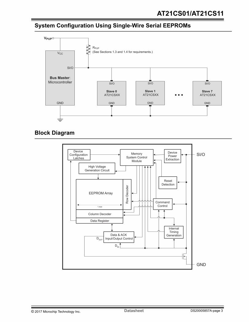
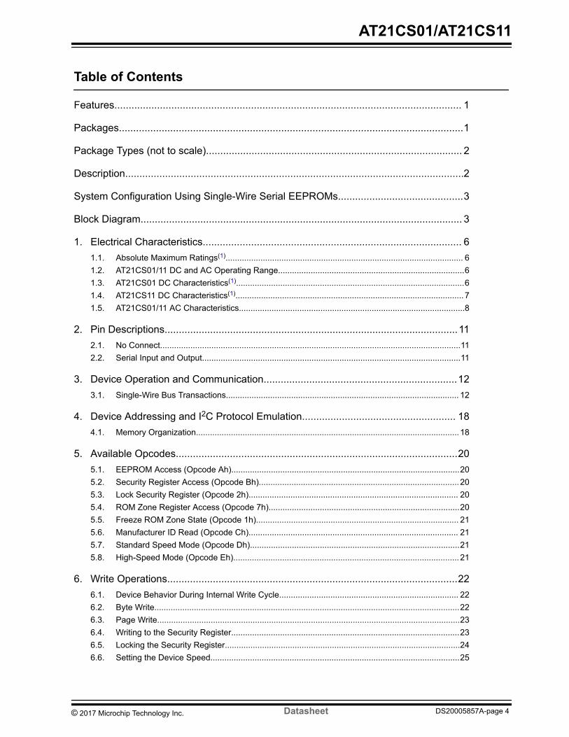
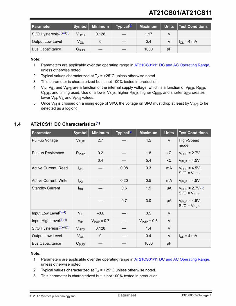
Parameter Symbol Minimum Typical(2) Maximum Units Test Conditions
SIO Hysteresis(3)(4)(5) VHYS 0128 mdash 117 V
Output Low Level VOL 0 mdash 04 V IOL = 4 mA
Bus Capacitance CBUS mdash mdash 1000 pF
Note 1 Parameters are applicable over the operating range in AT21CS0111 DC and AC Operating Range
unless otherwise noted2 Typical values characterized at TA = +25degC unless otherwise noted3 This parameter is characterized but is not 100 tested in production4 VIH VIL and VHYS are a function of the internal supply voltage which is a function of VPUP RPUP
CBUS and timing used Use of a lower VPUP higher RPUP higher CBUS and shorter tRCV createslower VIH VIL and VHYS values
5 Once VIH is crossed on a rising edge of SIO the voltage on SIO must drop at least by VHYS to bedetected as a logic lsquo0rsquo
14 AT21CS11 DC Characteristics(1)
Parameter Symbol Minimum Typical(2) Maximum Units Test Conditions
Pull-up Voltage VPUP 27 mdash 45 V High-Speedmode
Pull-up Resistance RPUP 02 mdash 18 kΩ VPUP = 27V
04 mdash 54 kΩ VPUP = 45V
Active Current Read IA1 mdash 008 03 mA VPUP = 45VSIO = VPUP
Active Current Write IA2 mdash 020 05 mA VPUP = 45V
Standby Current ISB mdash 06 15 microA VPUP = 27V(3)SIO = VPUP
mdash 07 30 microA VPUP = 45VSIO = VPUP
Input Low Level(3)(4) VIL ndash06 mdash 05 V
Input High Level(3)(4) VIH VPUP x 07 mdash VPUP + 05 V
SIO Hysteresis(3)(4)(5) VHYS 0128 mdash 14 V
Output Low Level VOL 0 mdash 04 V IOL = 4 mA
Bus Capacitance CBUS mdash mdash 1000 pF
Note 1 Parameters are applicable over the operating range in AT21CS0111 DC and AC Operating Range
unless otherwise noted2 Typical values characterized at TA = +25degC unless otherwise noted3 This parameter is characterized but is not 100 tested in production
AT21CS01AT21CS11
copy 2017 Microchip Technology Inc Datasheet DS20005857A-page 7
4 VIH VIL and VHYS are a function of the internal supply voltage which is a function of VPUP RPUPCBUS and timing used Use of a lower VPUP higher RPUP higher CBUS and shorter tRCV createslower VIH VIL and VHYS values
5 Once VIH is crossed on a rising edge of SIO the voltage on SIO must drop at least by VHYS to bedetected as a logic lsquo0rsquo
15 AT21CS0111 AC Characteristics
151 Reset and Discovery Response Timing
Parameter and Condition(1)(2) Symbol StandardSpeed(3)(4)
High Speed Units
Min Max Min Max
Reset Low Time Device in InactiveState
tRESET 480 mdash 48 mdash micros
Discharge Low Time Device in ActiveWrite Cycle (tWR)
tDSCHG 150 mdash 150 mdash micros
Reset Recovery Time tRRT NA NA 8 mdash micros
Discovery Response Request tDRR NA NA 1 2 - tPUP(5) micros
Discovery Response AcknowledgeTime
tDACK NA NA 8 24 micros
Master Strobe Discovery ResponseTime
tMSDR NA NA 2 6 micros
SIO High Time for StartStopCondition
tHTSS NA NA 150 mdash micros
Note 1 Parameters applicable over operating range in AT21CS0111 DC and AC Operating Range unless
otherwise noted2 AC measurement conditions for the table above
ndash Loading capacitance on SIO 100 pFndash RPUP (bus line pull-up resistor to VPUP) 1 kΩ VPUP 27V
3 Due to the fact that the device will default to High-Speed mode upon Reset the Reset andDiscovery Response Timing after tRESET does not apply for Standard Speed mode High-Speedmode timing applies in all cases after tRESET
4 Standard Speed is not available on the AT21CS115 tPUP is the time required once the SIO line is released to be pulled up from VIL to VIH This value is
application specific and is a function of the loading capacitance on the SIO line as well as the RPUPchosen Limits for these values are provided in AT21CS01 DC Characteristics(1) and AT21CS11DC Characteristics(1)
AT21CS01AT21CS11
copy 2017 Microchip Technology Inc Datasheet DS20005857A-page 8
152 Data Communication Timing
Parameter and Condition(1)(2) Symbol Frame Type StandardSpeed(3)
High Speed Units
Min Max Min Max
Bit Frame Duration tBIT Input andOutput Bit
Frame
40 100 tLOW0 +tPUP
(4) +tRCV
25 micros
SIO High Time for StartStopCondition
tHTSS Input BitFrame
600 mdash 150 mdash micros
SIO Low Time Logic lsquo0rsquoCondition
tLOW0 Input BitFrame
24 64 6 16 micros
SIO Low Time Logic lsquo1rsquoCondition
tLOW1 Input BitFrame
4 8 1 2 micros
Master SIO Low Time DuringRead
tRD Output BitFrame
4 8 -tPUP
(4)1 2 -
tPUP(4)
micros
Master Read Strobe Time tMRS Output BitFrame
tRD +tPUP
(4)8 tRD +
tPUP(4)
2 micros
Data Output Hold Time (Logiclsquo0rsquo)
tHLD0 Output BitFrame
8 24 2 6 micros
Slave Recovery Time tRCV Input andOutput Bit
Frame
8 mdash 2(5) mdash micros
Noise Filtering Capability onSIO
tNOISE Input BitFrame
05 mdash mdash mdash micros
Note 1 Parameters applicable over operating range in AT21CS0111 DC and AC Operating Range unless
otherwise noted2 AC measurement conditions for the table above
ndash Loading capacitance on SIO 100 pFndash RPUP (bus line pull-up resistor to VPUP) 1 kΩ VPUP 27V
3 Standard Speed is not available on the AT21CS114 tPUP is the time required once the SIO line is released to be pulled up from VIL to VIH This value is
application specific and is a function of the loading capacitance on the SIO line as well as the RPUPchosen Limits for these values are provided in AT21CS01 DC Characteristics(1)
5 The system designer must select an combination of RPUP CBUS and tBIT such that the minimumtRCV is satisfied The relationship of tRCV within the bit frame can be expressed by the followingformula tBIT = tLOW0 + tPUP + tRCV
AT21CS01AT21CS11
copy 2017 Microchip Technology Inc Datasheet DS20005857A-page 9
153 EEPROM Cell Performance Characteristics
Operation Min Max Units Test Condition
Write Cycle Time(tWR)
mdash 5 ms VPUP (min) lt VPUP lt VPUP (max)TA = 25degC Byte or Page Write mode
Write Endurance(1) 1000000 mdash Write Cycles VPUP (min) lt VPUP lt VPUP (max)TA = 25degC Byte or Page Write mode
Data Retention(2) 100 mdash Years VPUP (min) lt VPUP lt VPUP (max)TA = 55degC
Note 1 Write endurance performance is determined through characterization and the qualification process2 The data retention capability is determined through qualification and checked on each device in
production
AT21CS01AT21CS11
copy 2017 Microchip Technology Inc Datasheet DS20005857A-page 10
2 Pin DescriptionsThe descriptions of the pins are listed in Table 2-1
Table 2-1 Pin Function Table
Name 2-pad XSFN 3-lead SOT23 8-lead SOIC 4-ball WLCSP Function
NC mdash mdash 1 mdash No Connect
NC mdash mdash 2 mdash No Connect
NC mdash 2 3 mdash No Connect
GND 2 3 4 B1 Ground
SIO 1 1 5 A1 Serial Input andOutput
NC mdash mdash 6 No Connect
NC mdash mdash 7 mdash No Connect
NC mdash mdash 8 mdash No Connect
21 No ConnectThe NC pins are not internally connected These pins can be connected to GND or left floating
22 Serial Input and OutputThe SIO pin is an open-drain bidirectional inputoutput pin used to serially transfer data to and from thedevice
The SIO pin must be pulled high using an external pull‑up resistor (not to exceed 4 kΩ in value) and maybe wire-ORed with any number of other open‑drain or open‑collector pins from other devices on the samebus
The device also uses the SIO pin as its voltage source by drawing and storing power during the periodsthat the pin is pulled high to a voltage level between 17V and 36V (AT21CS01) and between 27V and45V (AT21CS11)
AT21CS01AT21CS11
copy 2017 Microchip Technology Inc Datasheet DS20005857A-page 11
3 Device Operation and CommunicationThe AT21CS0111 operates as a slave device and utilizes a single‑wire digital serial interface tocommunicate with a host controller commonly referred to as the bus master The master controls all readand write operations to the slave devices on the serial bus The device has two speeds of operationStandard Speed mode (AT21CS01) and High-Speed mode (AT21CS01 and AT21CS11)
The device utilizes an 8-bit data structure Data is transferred to and from the device via the single‑wireserial interface using the Serial InputOutput (SIO) pin Power to the device is also provided via the SIOpin thus only the SIO pin and the GND pin are required for device operation Data sent to the deviceover the single‑wire bus is interpreted by the state of the SIO pin during specific time intervals or slotsEach time slot is referred to as a bit frame and lasts tBIT in duration The master initiates all bit frames bydriving the SIO line low All commands and data information are transferred with the Most Significant bit(MSb) first
The software sequence sent to the device is an emulation of what would be sent to an I2C SerialEEPROM with the exception that typical 4-bit device type identifier of 1010b in the device address isreplaced by a 4-bit opcode The device has been architected in this way to allow for rapid deploymentand significant reuse of existing I2C firmware For more details about the way the device operates referto Device Addressing and I2C Protocol Emulation
During bus communication one data bit is transmitted in every bit frame and after eight bits (one byte) ofdata has been transferred the receiving device must respond with either an acknowledge (ACK) or a no-acknowledge (NACK) response bit during a ninth bit window There are no unused clock cycles duringany read or write operation so there must not be any interruptions or breaks in the data stream duringeach data byte transfer and ACK or NACK clock cycle In the event where an unavoidable systeminterrupt is required refer to the requirements outlined in Communication Interruptions
31 Single-Wire Bus TransactionsTypes of data transmitted over the SIO line
bull Reset and Discovery Responsebull Logic lsquo0rsquo or Acknowledge (ACK)bull Logic lsquo1rsquo or No Acknowledge (NACK)bull Start Conditionbull Stop Condition
The Reset and Discovery Response is not considered to be part of the data stream to the devicewhereas the remaining four transactions are all required in order to send data to and receive data fromthe device The difference between the different types of data stream transactions is the duration thatSIO is driven low within the bit frame
311 Device ResetPower-up and Discovery Response
3111 Resetting the DeviceA Reset and Discovery Response sequence is used by the master to reset the device as well as toperform a general bus call to determine if any devices are present on the bus
To begin the Reset portion of the sequence the master must drive SIO low for a minimum time If thedevice is not currently busy with other operations the master can drive SIO low for a time of tRESET Thelength of tRESET differs for Standard Speed mode and for High-Speed mode
AT21CS01AT21CS11
copy 2017 Microchip Technology Inc Datasheet DS20005857A-page 12
However if the device is busy the master must drive SIO for a longer time of tDSCHG to ensure the deviceis reset as discussed in Interrupting the Device during an Active Operation The Reset time forces anyinternal charge storage within the device to be consumed causing the device to lose all remainingstandby power available internally
Upon SIO being released for a sufficient amount of time to allow the device time to power-up andinitialize the master must then always request a Discovery Response Acknowledge from theAT21CS0111 prior to any commands being sent to the device The master can then determine if anAT21CS0111 is present by sampling for the Discovery Response Acknowledge from the device
3112 Device Response Upon Reset or Power-UpAfter the device has been powered up or after the master has reset the device by holding the SIO linelow for tRESET or tDSCHG the master must then release the line which will be pulled high by an externalpull-up resistor The master must then wait an additional minimum time of tRRT before the master canrequest a Discovery Response Acknowledge from the device
The Discovery Response Acknowledge sequence begins by the master driving the SIO line low whichwill start the AT21CS0111 internal timing circuits The master must continue to drive the line low for tDRR
During the tDRR time the AT21CS0111 will respond by concurrently driving SIO low The device willcontinue to drive SIO low for a total time of tDACK The master should sample the state of the SIO line attMSDR past the initiation of tDRR By definition the tDACK minimum is longer than the tMSDR maximum timethereby ensuring the master can always correctly sample the SIO for a level less than VIL After the tDACKtime has elapsed the AT21CS0111 will release SIO which will then be pulled high by the externalpull‑up resistor
The master must then wait tHTSS to create a Start condition before continuing with the first command (see StartStop Condition for more details about Start conditions) By default the device will come out of Resetin High-Speed mode Changing the device to Standard Speed mode is covered in Standard Speed Mode(Opcode Dh) The AT21CS0111 will power-up with its internal Address Pointer set to zero
The timing requirements for the Reset and Discovery Response sequence for both Standard Speed andHigh-Speed mode can be found in AT21CS0111 AC Characteristics
312 Interrupting the Device during an Active OperationTo conserve the stored energy within the onboard parasitic power system and minimize overall activecurrent the AT21CS0111 will not monitor the SIO line for new commands while it is busy executing apreviously sent command As a result the device is not able to sense how long SIO has been in a givenstate If the master requires to interrupt the device during an active operation it must drive SIO low longenough to deplete all of its remaining stored power This time is defined as tDSCHG after which a normalDiscovery Response can begin by releasing the SIO line
Figure 3-1 Reset and Discovery Response Waveform
SIO
tRESET tDSCHG
VIL
VIH
MASTER PULL-UP RESISTORAT21CS01
Begin Next Command with Start Condition
tRRT
tDACK
tMSDR
MasterSamplingWindow
tDRR
tPUPtHTSS
AT21CS01AT21CS11
copy 2017 Microchip Technology Inc Datasheet DS20005857A-page 13
313 Data Input and Output Bit FramesCommunication with the AT21CS0111 is conducted in time intervals referred to as a bit frame and laststBIT in duration Each bit frame contains a single binary data value Input bit frames are used to transmitdata from the master to the AT21CS0111 and can either be a logic lsquo0rsquo or a logic lsquo1rsquo An output bit framecarries data from the AT21CS0111 to the master In all input and output cases the master initiates the bitframe by driving the SIO line low Once the AT21CS0111 detects the SIO being driven below the VILlevel its internal timing circuits begin to run
The duration of each bit frame is allowed to vary from bit to bit as long as the variation does not cause thetBIT length to exceed the specified minimum and maximum values (see AT21CS0111 ACCharacteristics) The tBIT requirements will vary depending on whether the device is set for Low-Speed orHigh-Speed mode For more information about setting the speed of the device refer to Setting the DeviceSpeed
3131 Data Input Bit FramesA data input bit frame can be used by the master to transmit either a logic lsquo0rsquo or logic lsquo1rsquo data bit to theAT21CS0111 The input bit frame is initiated when the master drives the SIO line low The length of timethat the SIO line is held low will dictate whether the master is transmitting a logic lsquo0rsquo or a logic lsquo1rsquo for thatbit frame For a logic lsquo0rsquo input the length of time that the SIO line must be held low is defined as tLOW0Similarly for a logic lsquo1rsquo input the length of time that the SIO line must be held low is defined as tLOW1
The AT21CS0111 will sample the state of the SIO line after the maximum tLOW1 but prior to the minimumtLOW0 after SIO was driven below the VIL threshold to determine if the data input is a logic lsquo0rsquo or alogic lsquo1rsquo If the master is still driving the line low at the sample time the AT21CS0111 will decode that bitframe as a logic lsquo0rsquo as SIO will be at a voltage less than VIL If the master has already released the SIOline the AT21CS0111 will see a voltage level greater than or equal to VIH because of the external pull-upresistor and that bit frame will be decoded as a logic lsquo1rsquo The timing requirements for these parameterscan be found in AT21CS0111 AC Characteristics
A logic lsquo0rsquo condition has multiple uses in the I2C emulation sequences It is used to signify a lsquo0rsquo data bitand it also is used for an Acknowledge (ACK) response Additionally a logic lsquo1rsquo condition is also is usedfor a No Acknowledge (NACK) response in addition to the nominal lsquo1lsquo data bit
Figure 3-2 and Figure 3-3 depict the logic lsquo0rsquo and logic lsquo1rsquo input bit frames
Figure 3-2 Logic 0 Input Condition Waveform
SIO
tLOW0
VIL
VIH
tBIT
MASTER PULL-UP RESISTOR
tRCV
AT21CS01AT21CS11
copy 2017 Microchip Technology Inc Datasheet DS20005857A-page 14
Figure 3-3 Logic 1 Input Condition Waveform
SIO
tLOW1
VIL
VIH
tBIT
MASTER PULL-UP RESISTOR
3132 StartStop ConditionAll transactions to the AT21CS0111 begin with a Start condition therefore a Start can only betransmitted by the master to the slave Likewise all transactions are terminated with a Stop condition andthus a Stop condition can only be transmitted by the master to the slave
The Start and Stop conditions require identical biasing of the SIO line The StartStop condition iscreated by holding the SIO line at a voltage of VPUP for a duration of tHTSS Refer to AT21CS0111 ACCharacteristics for timing minimums and maximums
Figure 3-4 and Figure 3-5 depict the Start and Stop conditions
Figure 3-4 Start Condition Waveform
SIOVIL
VIH
tHTSS
MASTER PULL-UP RESISTOR
Figure 3-5 Stop Condition Waveform
SIOVIL
VIH
tHTSS
MASTER PULL-UP RESISTOR
PreviousBit Frame
tRCV
3133 Communication InterruptionsIn the event that a protocol sequence is interrupted midstream this sequence can be resumed at thepoint of interruption if the elapsed time of inactivity (where SIO is idle) is less that the maximum tBIT timeThe maximum allowed value will differ if the device is High-Speed mode or Low-Speed mode (see Settingthe Device Speed)
AT21CS01AT21CS11
copy 2017 Microchip Technology Inc Datasheet DS20005857A-page 15
Note The interruption of protocol must not occur during a write sequence immediately after a logic lsquo0rsquoldquoACKrdquo response when sending data to be written to the device In this case the interruption will beinterpreted as a Stop condition and will cause an internal write cycle to begin The device will be busy fortWR time and will not respond to any commands
Note For systems that cannot accurately monitor the location of interrupts it is recommended to ensurethat a minimum interruption time be observed consistent with the longest busy operation of the device(tWR) Communicating with the device while it is in an internal write cycle by the master driving SIO lowcould cause the byte(s) being written to become corrupted and must be avoided The behavior of thedevice during a write cycle is described in more detail in Device Behavior During Internal Write Cycle
If the sequence is interrupted for longer than the maximum tBIT the master must wait at least theminimum tHTSS before continuing By waiting the minimum tHTSS time a new Start condition is createdand the device is ready to receive a new command It is recommended that the master start over andrepeat the transaction that was interrupted midstream
3134 Data Output Bit FrameA data output bit frame is used when the master is to receive communication back from theAT21CS0111 Data output bit frames are used when reading any data out as well as any ACK or NACKresponses from the device Just as in the input bit frame the master initiates the sequence by driving theSIO line below the VIL threshold which engages the AT21CS0111 internal timing generation circuit
Within the output bit frame is the critical timing parameter tRD which is defined as the amount of time themaster must continue to drive the SIO line low after crossing the below VIL threshold to request a data bitback from the AT21CS0111 Once the tRD duration has expired the master must release the SIO line
If the AT21CS0111 is responding with a logic lsquo0rsquo (for either a lsquo0rsquo data bit or an ACK response) it will beginto pull the SIO line low concurrently during the tRD window and continue to hold it low for a duration oftHLD0 after which it will release the line to be pulled back up to VPUP (see Figure 3-6) Thus when themaster samples SIO within the tMRS window it will see a voltage less than VIL and decode this event as alogic rsquo0rsquo By definition the tHLD0 time is longer than the tMRS time and therefore the master is ensured tosample while the AT21CS0111 is still driving the SIO line low
Figure 3-6 Logic 0 Data Output Bit Frame Waveform
AT21CS01 [DATASHEET]Atmel-8903A-SEEPROM-AT21CS01-Datasheet_082015
10
3134 Data Output Bit FrameA data output Bit Frame is used when the Master is to receive communication back from the AT21CS01 Data output Bit Frames are used when reading any data out as well as any ACK or NACK responses from the deviceJust as in the input Bit Frame the Master initiates the sequence by driving the SIO line below the VIL threshold which engages the AT21CS01rsquos internal timing generation circuit Within the output Bit Frame is the critical timing parameter tRD which is defined as the amount of time the Master must continue to drive the SIO line low after crossing the below VIL threshold to request a data bit back from the AT21CS01 Once the tRD duration has expired the Master must release the SIO line If the AT21CS01 is responding with a Logic 0 (for either a lsquo0rsquo data bit or an ACK response) it will begin to pull the SIO line low concurrently during the tRD window and continue to hold it low for a duration of tHLD0 after which it will release the line to be pulled back up to VPUP (see Figure 3-6) Thus when the Master samples SIO within the tMRS window it will see a voltage less than VIL and decode this event as a Logic 0 By definition the tHLD0 time is longer than the tMRS time and therefore the Master is guaranteed to sample while the AT21CS01 is still driving the SIO line low
Figure 3-6 Logic 0 Data Output Bit Frame Waveform
If the AT21CS01 intends to respond with a Logic 1 (for either a lsquo1rsquo data bit or a NACK response) it will not drive the SIO line low at all Once the Master releases the SIO line after the maximum tRD has elapsed the line will be pulled up to VPUP Thus when the Master samples the SIO line within the tMRS window it will detect a voltage greater than VIH and decode this event as a Logic 1The data output Bit Frame is shown in greater detail below in Figure 3-7
Figure 3-7 Logic 1 Data Output Bit Frame Waveform
SIOVIL
VIH
tBIT
MASTER PULL-UP RESISTOR
tMRS
tRCV
AT21CS01
MasterSamplingWindowtRD
tHLD0
tPUP
SIOVIL
VIH
tBIT
MASTER PULL-UP RESISTOR
tMRS
AT21CS01
MasterSamplingWindowtRD
tPUP
Note AT21CS01 will not drive the SIO line during a Logic 1 output Bit Frame
If the AT21CS0111 intends to respond with a logic lsquo1rsquo (for either a lsquo1rsquo data bit or a NACK response) it willnot drive the SIO line low at all Once the master releases the SIO line after the maximum tRD haselapsed the line will be pulled up to VPUP Thus when the master samples the SIO line within the tMRSwindow it will detect a voltage greater than VIH and decode this event as a logic lsquo1rsquo
The data output bit frame is shown in greater detail below in Figure 3-7
AT21CS01AT21CS11
copy 2017 Microchip Technology Inc Datasheet DS20005857A-page 16
Figure 3-7 Logic 1 Data Output Bit Frame Waveform
AT21CS01 [DATASHEET]Atmel-8903A-SEEPROM-AT21CS01-Datasheet_082015
10
3134 Data Output Bit FrameA data output Bit Frame is used when the Master is to receive communication back from the AT21CS01 Data output Bit Frames are used when reading any data out as well as any ACK or NACK responses from the deviceJust as in the input Bit Frame the Master initiates the sequence by driving the SIO line below the VIL threshold which engages the AT21CS01rsquos internal timing generation circuit Within the output Bit Frame is the critical timing parameter tRD which is defined as the amount of time the Master must continue to drive the SIO line low after crossing the below VIL threshold to request a data bit back from the AT21CS01 Once the tRD duration has expired the Master must release the SIO line If the AT21CS01 is responding with a Logic 0 (for either a lsquo0rsquo data bit or an ACK response) it will begin to pull the SIO line low concurrently during the tRD window and continue to hold it low for a duration of tHLD0 after which it will release the line to be pulled back up to VPUP (see Figure 3-6) Thus when the Master samples SIO within the tMRS window it will see a voltage less than VIL and decode this event as a Logic 0 By definition the tHLD0 time is longer than the tMRS time and therefore the Master is guaranteed to sample while the AT21CS01 is still driving the SIO line low
Figure 3-6 Logic 0 Data Output Bit Frame Waveform
If the AT21CS01 intends to respond with a Logic 1 (for either a lsquo1rsquo data bit or a NACK response) it will not drive the SIO line low at all Once the Master releases the SIO line after the maximum tRD has elapsed the line will be pulled up to VPUP Thus when the Master samples the SIO line within the tMRS window it will detect a voltage greater than VIH and decode this event as a Logic 1The data output Bit Frame is shown in greater detail below in Figure 3-7
Figure 3-7 Logic 1 Data Output Bit Frame Waveform
SIOVIL
VIH
tBIT
MASTER PULL-UP RESISTOR
tMRS
tRCV
AT21CS01
MasterSamplingWindowtRD
tHLD0
tPUP
SIOVIL
VIH
tBIT
MASTER PULL-UP RESISTOR
tMRS
AT21CS01
MasterSamplingWindowtRD
tPUP
Note AT21CS01 will not drive the SIO line during a Logic 1 output Bit Frame
AT21CS01AT21CS11
copy 2017 Microchip Technology Inc Datasheet DS20005857A-page 17
4 Device Addressing and I2C Protocol EmulationAccessing the device requires a Start condition followed by an 8-bit device address word
The AT21CS0111 protocol sequence emulates what would be required for an I2C Serial EEPROM withthe exception that the beginning four bits of the device address are used as an opcode for the differentcommands and actions that the device can perform
Since multiple slave devices can reside on the bus each slave device must have its own unique addressso that the master can access each device independently After the 4-bit opcode the following three bitsof the device address byte are comprised of the slave address bits The three slave address bits arepreprogrammed prior to shipment and are read-only Obtaining devices with different slave address bitvalues is done by purchasing a specific ordering code Refer to Packaging Information for explanation ofwhich ordering code corresponds with a specific slave address value
Following the three slave address bits is a ReadWrite select bit where a logic lsquo1rsquo indicates a read and alogic lsquo0rsquo indicates a write Upon the successful comparison of the device address the EEPROM will returnan ACK (logic lsquo0rsquo) If the 4-bit opcode is invalid or the three bits of slave address do not match what ispreprogrammed in the device the device will not respond on the SIO line and will return to a Standbystate
Table 4-1 Device Address Byte
4-bit Opcode Preprogrammed Slave Address Bits ReadWrite
Bit 7 Bit 6 Bit 5 Bit 4 Bit 3 Bit 2 Bit 1 Bit 0
Refer to Available Opcodes A2 A1 A0 RW
Following the device address byte a memory address byte must be transmitted to the deviceimmediately The memory address byte contains a 7-bit memory array address to specify which locationin the EEPROM to start reading or writing Refer to Table 4-2 to review these bit positions
Table 4-2 Memory Address Byte
Bit 7 Bit 6 Bit 5 Bit 4 Bit 3 Bit 2 Bit 1 Bit 0
Donrsquot Care A6 A5 A4 A3 A2 A1 A0
41 Memory OrganizationThe AT21CS0111 internal memory array is partitioned into two regions The main 1-Kbit EEPROM isorganized as 16 pages of eight bytes each The Security register is 256 bits in length organized as fourpages of eight bytes each The lower two pages of the Security register are read-only and have afactory‑programmed 64‑bit serial number that is unique across all AT21CS series Serial EEPROMs Theupper two pages of the Security register are user-programmable and can be subsequently locked (see Locking the Security Register)
AT21CS01AT21CS11
copy 2017 Microchip Technology Inc Datasheet DS20005857A-page 18
Figure 4-1 Memory Architecture Diagram
Main1-Kbit
EEPROM
256-bitSecurityRegister
Zone 2
1-Kbit Address Range (00h-7Fh)
User-Programmable MemoryAddress Range (10h-1Fh)
64-bit Serial NumberAddress Range (00h-07h)
Permanently Lockableby Software
Opcode 1010b (Ah)
Opcode1011b (Bh)
Read-Only
Four 256-bit ROM Zones
Each can be independently
set to read-only
Zone 0
Zone 1
Zone 2
Zone 3
Reserved for Future UseAddress Range (08h-0Fh)
AT21CS01AT21CS11
copy 2017 Microchip Technology Inc Datasheet DS20005857A-page 19
5 Available OpcodesTable 5-1 outlines available opcodes for the AT21CS0111
Table 5-1 Opcodes used by the AT21CS0111
Command 4-Bit Opcode Brief Description of Functionality
EEPROM Access 1010 (Ah) ReadWrite the contents of the main memory array
Security Register Access 1011 (Bh) ReadWrite the contents of the Security register
Lock Security Register 0010 (2h) Permanently lock the contents of the Security register
ROM Zone RegisterAccess
0111 (7h) Inhibit further modification to a zone of the EEPROM array
Freeze ROM Zone State 0001 (1h) Permanently lock the current state of the ROM Zoneregisters
Manufacturer ID Read 1100 (Ch) Query manufacturer and density of device
Standard Speed Mode 1101 (Dh) Switch to Standard Speed mode operation (AT21CS01only command the AT21CS11 will NACK this command)
High-Speed Mode 1110 (Eh) Switch to High-Speed mode operation (AT21CS0111power‑on default AT21CS11 will ACK this command)
51 EEPROM Access (Opcode Ah)The opcode Ah is used to read data from and write data to the EEPROM Refer to Read Operations formore details about reading data from the device For details about writing to the EEPROM refer to WriteOperations
52 Security Register Access (Opcode Bh)The opcode Bh is used to read data from and write data to the Security register Refer to ReadOperations in the Security Register for more details about reading data from the Security register Fordetails about writing to the user-programmable portion of the Security register refer to section Writing tothe Security Register
53 Lock Security Register (Opcode 2h)The opcode 2h is used to permanently lock the user-programmable portion of the Security register Referto Locking the Security Register
54 ROM Zone Register Access (Opcode 7h)The AT21CS0111 is partitioned into four 256-bit zones each of which can be independently andpermanently made read-only (ROM) The state of each zone is stored in a Configuration register whichcan be read from or written to using the opcode 7h The ROM Zone functionality is explained in greaterdetail in ROM Zones
AT21CS01AT21CS11
copy 2017 Microchip Technology Inc Datasheet DS20005857A-page 20
55 Freeze ROM Zone State (Opcode 1h)The opcode 1h is used to permanently freeze the current state of the ROM Zone registers Once set theROM Zone registers are read-only
Therefore any zone that is not already read-only cannot be subsequently converted to ROM Refer to Freeze ROM Zone Registers for additional details
56 Manufacturer ID Read (Opcode Ch)Manufacturer identification device density and device revision information can be read from the deviceusing the opcode Ch The full details of the format of the data returned by this command are found in Manufacturer ID Read
57 Standard Speed Mode (Opcode Dh)The AT21CS01 can be set to Standard Speed mode or checked to see whether or not it is in StandardSpeed mode with the use of the Dh opcode Further details are covered in Standard Speed Mode(AT21CS01) The AT21CS11 does not offer Standard Speed mode and therefore will NACK thiscommand
58 High-Speed Mode (Opcode Eh)The AT21CS01 can be set to High-Speed mode or checked to see whether or not it is in High-Speedmode with the use of the Eh opcode The AT21CS11 only operates in High-Speed mode and thereforewill ACK this command Further details are covered in High-Speed Mode
AT21CS01AT21CS11
copy 2017 Microchip Technology Inc Datasheet DS20005857A-page 21
6 Write OperationsAll write operations for the AT21CS0111 begin with the master sending a Start condition followed by adevice address byte (opcode Ah for the EEPROM and opcode Bh for the Security register) with the RWbit set to lsquo0rsquo followed by the memory address byte Next the data value(s) to be written to the device aresent Data values must be sent in 8-bit increments to the device followed by a Stop condition If a Stopcondition is sent somewhere other than at the byte boundary the current write operation will be aborted
The AT21CS0111 allows single byte writes partial page writes and full page writes
61 Device Behavior During Internal Write CycleTo ensure that the address and data sent to the device for writing are not corrupted while any type ofinternal write operation is in progress commands sent to the device are blocked from being recognizeduntil the internal operation is completed If a write interruption occurs (SIO pulsed low) and is smallenough to not deplete the internal power storage the device will NACK signaling that the operation is inprogress If an interruption is longer than tDSCHG then internal write operation will be terminated and mayresult in data corruption
62 Byte WriteThe AT21CS0111 supports writing of a single 8-bit byte and requires a 7-bit memory word address toselect which byte to write
Upon receipt of the proper device address byte (with opcode of Ah) and memory address byte theEEPROM will send a logic lsquo0rsquo to signify an ACK The device will then be ready to receive the data byteFollowing receipt of the complete 8-bit data byte the EEPROM will respond with an ACK A Stopcondition must then occur however since a Stop condition is defined as a null bit frame with SIO pulledhigh the master does not need to drive the SIO line to accomplish this If a Stop condition is sent at anyother time the write operation is aborted After the Stop condition is complete the EEPROM will enter aninternally self-timed write cycle which will complete within a time of tWR while the data is beingprogrammed into the nonvolatile EEPROM The SIO pin must be pulled high via the external pull-upresistor during the entire tWR cycle After the maximum tWR time has elapsed the master may begin anew bus transactionNote
1 Any attempt to interrupt the internal write cycle by driving the SIO line low may cause the bytebeing programmed to be corrupted Other memory locations within the memory array will not beaffected Note Device Behavior During Internal Write Cycle for the behavior of the device while thewrite cycle is in progress If the master must interrupt a write operation the SIO line must be drivenlow for tDSCHG as noted in Interrupting the Device during an Active Operation
Figure 6-1 Byte Write
SIOMSB
ACKby Slave
1 0 1 0 A2 A1 A0 0
Device Address
MSB
x A6 A5 A4 A3 A2 A1 A0
Memory Address
MSB
D D D D D D D D
Data In Byte
ACKby Slave
`ACKby Slave
Stop Conditionby Master
Start Conditionby Master
0 0 0
Note 1 x = Donrsquot Care bit in the place of A7 as this bit falls outside the 1-Kbit addressable range
AT21CS01AT21CS11
copy 2017 Microchip Technology Inc Datasheet DS20005857A-page 22
63 Page WriteA page write operation allows up to eight bytes to be written in the same write cycle provided all bytesare in the same row (address bits A6 through A3 are the same) of the memory array Partial page writesof less than eight bytes are allowed
A page write is initiated the same way as a byte write but the bus master does not send a Stop conditionafter the first data byte is clocked in Instead after the EEPROM acknowledges receipt of the first databyte the bus master can transmit up to an additional seven data bytes
The EEPROM will respond with an ACK after each data byte is received Once all data bytes have beensent the device requires a Stop condition to begin the write cycle However since a Stop condition isdefined as a null bit frame with SIO pulled high the master does not need to drive the SIO line toaccomplish this If a Stop condition is sent at any other time the write operation is aborted After the Stopcondition is complete the internally self-timed write cycle will beginThe SIO pin must be pulled high viathe external pull-up resistor during the entire tWR cycle Thus in a multi‑slave environmentcommunication to other single-wire devices on the bus should not be attempted while any devices are inan internal write cycle
The lower three bits of the memory address are internally incremented following the receipt of each databyte The higher order address bits are not incremented and the device retains the memory pagelocation Page write operations are limited to writing bytes within a single physical page regardless of thenumber of bytes actually being written When the incremented word address reaches the page boundarythe address counter will ldquoroll overrdquo to the beginning of the same page Nevertheless creating a roll overevent should be avoided as previously loaded data in the page could become unintentionally alteredAfter the maximum tWR time has elapsed the master may begin a new bus transaction
Note 1 Any attempt to interrupt the internal write cycle by driving the SIO line low may cause the bytes
being programmed to be corrupted Other memory locations within the memory array will not beaffected Note Device Behavior During Internal Write Cycle for the behavior of the device while thewrite cycle is in progress If the master must interrupt a write operation the SIO line must be drivenlow for tDSCHG as noted in Interrupting the Device during an Active Operation
Figure 6-2 Page Write
SIOMSB
ACKby Slave
1 0 1 0 A2 A1 A0 0
Device Address
MSB
x A6 A5 A4 A3 A2 A1 A0
Memory Address
MSB
D D D D D D D D
Data In Byte (1)
D D D D D D D D
Data In Byte (8)
ACKby Slave
ACKby Slave
ACKby Slave
Stop Conditionby Master
Start Conditionby Master
0000
Note 1 x = Donrsquot Care bit in the place of A7 as this bit falls outside the 1-Kbit addressable range
64 Writing to the Security RegisterThe Security register supports bytes writes page writes and partial page writes in the upper 16 bytes(upper two pages of eight bytes each) of the region Page writes and partial page writes in the Securityregister have the same page boundary restrictions and behavior requirements as they do in theEEPROM
Upon receipt of the proper device address byte (with opcode of Bh specified) and memory address bytethe EEPROM will send a logic lsquo0rsquo to signify an ACK The device will then be ready to receive the first databyte
AT21CS01AT21CS11
copy 2017 Microchip Technology Inc Datasheet DS20005857A-page 23
Following receipt of the data byte the EEPROM will respond with an ACK and the master can send up toan additional seven bytes if desired The EEPROM will respond with an ACK after each data byte issuccessfully received Once all of the data bytes have been sent the device requires a Stop condition tobegin the write cycle However since a Stop condition is defined as a null bit frame with SIO pulled highthe master does not need to drive the SIO line to accomplish this After the Stop condition is completethe EEPROM will enter an internally self-timed write cycle which will complete within a time of tWR whilethe data is being programmed into the nonvolatile EEPROM The SIO pin must be pulled high via theexternal pull-up resistor during the entire tWR cycle Figure 6-3 is included below as an example of a bytewrite operation in the Security register
Figure 6-3 Byte Write in the Security Register
SIOMSB
ACKby Slave
1 0 1 1 A2 A1 A0 0
Device Address
MSB
x x x 1 A3 A2 A1 A0
MSB
D D D D D D D D
Data In Byte
ACKby Slave
ACKby Slave
Stop Conditionby Master
Start Conditionby Master
0 0 0
Security Register Address
Note 1 x = Donrsquot Care values in the place of A7‑A5 as these bits falls outside the addressable range of the
Security register2 Any attempt to interrupt the internal write cycle by driving the SIO line low may cause the byte
being programmed to be corrupted Other memory locations within the memory array will not beaffected Note Device Behavior During Internal Write Cycle for the behavior of the device while thewrite cycle is in progress If the master must interrupt a write operation the SIO line must be drivenlow for tDSCHG as noted in Interrupting the Device during an Active Operation
65 Locking the Security RegisterThe Lock command is an irreversible sequence that will permanently prevent all future writing to theupper 16 bytes of the Security register on the AT21CS0111 Once the Lock command has beenexecuted the entire 32-byte Security register becomes read-only Once the Security register has beenlocked it is not possible to unlock it
The Lock command protocol emulates a byte write operation to the Security register however theopcode 0010b (2h) is required along with the A7 through A4 bits of the memory address being set to0110b (6h) The remaining bits of the memory address as well as the data byte are donrsquot care bitsEven though these bits are donrsquot cares they still must be transmitted to the device An ACK response tothe memory address and data byte indicates the Security register is not currently locked A NACKresponse indicates the Security register is already locked Refer to Figure 6-5 for details aboutdetermining the Lock status of the Security register
The sequence completes with a Stop condition to initiate a self-timed internal write cycle If a Stopcondition is sent at any other time the Lock operation is aborted Since a Stop condition is defined as anull bit frame with SIO pulled high the master does not need to drive the SIO line to accomplish thisUpon completion of the write cycle (taking a time of tWR) the Lock operation is complete and the Securityregister will become permanently read-only
Note 1 Any attempt to drive the SIO line low during the tWR time period may cause the Lock operation to
not complete successfully and must be avoided
AT21CS01AT21CS11
copy 2017 Microchip Technology Inc Datasheet DS20005857A-page 24
Figure 6-4 Lock Command
SIOMSB
ACKby Slave
0 0 1 0 A2 A1 A0 0
Device Address
MSB
0 1 1 0 X X X X
Lock Security Register Address
MSB
X X X X X X X X
Data In Byte
ACKby Slave
ACKby Slave
Stop Conditionby Master
Start Conditionby Master
0 0 0
651 Device Response to a Write Command on a Locked DeviceA locked device will respond differently to a Write command to the Security register compared to a devicethat has not been locked Writing to the Security register is accomplished by sending a Start conditionfollowed by a device address byte with the opcode of 1011b (Bh) the appropriate slave addresscombination and the ReadWrite bit set as a logic lsquo0rsquo Both a locked device and a device that has notbeen locked will return an ACK Next the 8-bit word address is sent and again both devices will return anACK However upon sending the data input byte a device that has already been locked will return aNACK and be immediately ready to accept a new command whereas a device that has not been lockedwill return an ACK to the data input byte as per normal operation for a Write command as described in Write Operations
652 Check Lock CommandThe Check Lock command follows the same sequence as the Lock command (including 0110b in the A7through A4 bits of the memory address byte) with the exception that only the device address byte andmemory address byte need to be transmitted to the device An ACK response to the memory addressbyte indicates that the lock has not been set while a NACK response indicates that the lock has been setIf the lock has already been enabled it cannot be reversed The Check Lock command is completed bythe master sending a Stop bit to the device (defined as a null bit frame)
Figure 6-5 Check Lock Command
SIOMSB
ACKby Slave
0 0 1 0 A2 A1 A0 0
Device Address
MSB
0 1 1 0 X X X X
Lock Security Register Address
ACK by Slaveif Unlocked
NACK by Slaveif Locked
Stop Conditionby Master
Start Conditionby Master
0
66 Setting the Device SpeedThe AT21CS01 can be set to Standard Speed mode (154 kbps maximum) or High-Speed mode(125 kbps maximum) through a software sequence Upon executing a Reset and Discovery Responsesequence (see Device ResetPower-up and Discovery Response) the device will default to High-Speedmode The AT21CS11 does not have Standard Speed mode
661 Standard Speed Mode (AT21CS01)The AT21CS01 can be set to Standard Speed mode or checked to see whether or not it is in StandardSpeed mode with the use of the Dh opcode This transaction only requires eight bits
To set the device to Standard Speed mode the master must send a Start condition followed by thedevice address byte with the opcode of 1101b (Dh) specified along with the appropriate slave addresscombination and the ReadWrite bit set to a logic lsquo0rsquo The device will return an ACK (logic lsquo0rsquo) and will beimmediately ready to receive commands for standard speed operation
AT21CS01AT21CS11
copy 2017 Microchip Technology Inc Datasheet DS20005857A-page 25
To determine if the device is already set to Standard Speed mode the device address byte with theopcode of 1101b (Dh) must be sent to the device along with the appropriate slave address combinationand the ReadWrite bit set to a logic lsquo1rsquo The device will return an ACK (logic lsquo0rsquo) if it was set for StandardSpeed mode It will return a NACK (logic lsquo1rsquo) if the device was not currently set for Standard Speed mode
Note The AT21CS11 will NACK this command
662 High-Speed ModeThe device can be set to High-Speed mode or checked to see whether or not it is in High-Speed modewith the use of the Eh opcode This transaction only requires eight bits The power-on default for theAT21CS0111 is High-Speed mode
To set the device to High-Speed mode the master must send a Start condition followed by the deviceaddress byte with the opcode of 1110b (Eh) specified along the appropriate slave address combinationand the ReadWrite bit set to a logic lsquo0rsquo The device will return an ACK (Logic 0) and will be immediatelyready to receive commands for high-speed operation
To determine if the device is already set to High-Speed mode the device address byte with the opcode of1110b (Eh) specified must be sent to the device along with the appropriate slave address combinationand the ReadWrite bit set to a logic lsquo1rsquo The device will return an ACK (logic lsquo0rsquo) if it was set for High-Speed mode It will return a NACK (logic lsquo1rsquo) if the device was not currently set for High-Speed mode
Note The AT21CS11 will ACK this command
AT21CS01AT21CS11
copy 2017 Microchip Technology Inc Datasheet DS20005857A-page 26
7 Read OperationsRead operations are initiated in a similar way as write operations with the exception that the ReadWriteselect bit in the device address byte must be set to a logic lsquo1rsquo There are multiple read operationssupported by the device
bull Current Address Read within the EEPROMbull Random Read within the EEPROMbull Sequential Read within the EEPROMbull Read from the Security Registerbull Manufacturer ID Read
Note 1 The AT21CS0111 contains a single shared-memory Address Pointer that maintains the
address of the next byte in the EEPROM or Security register to be accessed For example ifthe last byte read or written was memory location 0Dh of the EEPROM then the AddressPointer will be pointing to memory location 0Eh of the EEPROM As such when changingfrom a read in one region to the other the first read operation in the new region should beginwith a random read instead of a current address read to ensure the Address Pointer is set toa known value within the desired region
If the end of the EEPROM or the Security register is reached then the Address Pointer will ldquoroll overrdquoback to the beginning (address 00h) of that region The Address Pointer retains its value betweenoperations as long as the pull-up voltage on the SIO pin is maintained or as long as the device has notbeen reset
71 Current Address Read within the EEPROMThe internal Address Pointer must be pointing to a memory location within the EEPROM in order toperform a current address read from the EEPROM To initiate the operation the master must send a Startcondition followed by the device address byte with the opcode of 1010b (Ah) specified along with theappropriate slave address combination and the ReadWrite bit set to a logic lsquo1rsquo After the device addressbyte has been sent the AT21CS0111 will return an ACK (logic lsquo0rsquo)
Following the ACK the device is ready to output one byte (eight bits) of data The master initiates the allbits of data by driving the SIO line low to start The AT21CS0111 will hold the line low after the masterreleases it to indicate a logic lsquo0rsquo If the data is logic lsquo1rsquo the AT21CS0111 will not hold the SIO line low atall causing it to be pulled high by the pull-up resistor once the master releases it This sequence repeatsfor eight bits
After the master has read the first data byte and no further data is desired the master must return aNACK (logic lsquo1rsquo) response to end the read operation and return the device to the Standby mode Figure7-1 depicts this sequence
If the master would like the subsequent byte it would return an ACK (logic lsquo0rsquo) and the device will beready output the next byte in the memory array Refer to Sequential Read within the EEPROM for detailsabout continuing to read beyond one byte
Note 1 If the last operation to the device was an access to the Security register then a random read should
be performed to ensure that the Address Pointer is set to a known memory location within theEEPROM
AT21CS01AT21CS11
copy 2017 Microchip Technology Inc Datasheet DS20005857A-page 27
Figure 7-1 Current Address Read
SIOMSB
ACKby Slave
1 0 1 0 A2 A1 A0 1
Device Address
MSB
D D D D D D D D
Data Out Byte (n)
NACK by Master
Stop Conditionby Master
Start Conditionby Master
0 1
72 Random Read within the EEPROMA random read begins in the same way as a byte write operation which will load a new EEPROM memoryaddress into the Address Pointer However instead of sending the data byte and Stop condition of thebyte write a repeated Start condition is sent to the device This sequence is referred to as a ldquodummywriterdquo After the device address and memory address bytes of the ldquodummy writerdquo have been sent theAT21CS0111 will return an ACK response The master can then initiate a current address readbeginning with a new Start condition to read data from the EEPROM Refer to Current Address Readwithin the EEPROM for details on how to perform a current address read
Figure 7-2 Random Read
SIOMSB
ACKby Slave
1 0 1 0 A2 A1 A0 0
Device Address
Dummy Write
MSB
x A6 A5 A4 A3 A2 A1 A0
Memory Address
MSB
D D D D D D D D
Data Out Byte (n)
ACKby Slave
NACKby Master
Stop Conditionby Master
Start Conditionby Master
MSB
ACKby Slave
1 0 1 0 A2 A1 A0 1
Device Address
Restartby Master
1000
73 Sequential Read within the EEPROMSequential reads start as either a current address read or as a random read However instead of themaster sending a NACK (logic lsquo1rsquo) response to end a read operation after a single byte of data has beenread the master sends an ACK (logic lsquo0rsquo) to instruct the AT21CS0111 to output another byte of data Aslong as the device receives an ACK from the master after each byte of data has been output it willcontinue to increment the address counter and output the next byte data from the EEPROM If the end ofthe EEPROM is reached then the Address Pointer will ldquoroll overrdquo back to the beginning (address 00h) ofthe EEPROM region To end the sequential read operation the master must send a NACK response afterthe device has output a complete byte of data After the device receives the NACK it will end the readoperation and return to the Standby mode
Note 1 If the last operation to the device accessed the Security register then a random read should be
performed to ensure that the Address Pointer is set to a known memory location within theEEPROM
Figure 7-3 Sequential Read from a Current Address Read
SIOMSB
ACKby Slave
1 0 1 0 A2 A1 A0 1
Device Address
MSB
D D D D D D D D
Data Out Byte (n)
ACK by Master
MSB
D D D D D D D D
Data Out Byte (n+x)
NACK by Master
Stop Conditonby Master
Start Conditionby Master
0 0 1
AT21CS01AT21CS11
copy 2017 Microchip Technology Inc Datasheet DS20005857A-page 28
Figure 7-4 Sequential Read from a Random Read
SIOMSB
ACKby Slave
1 0 1 0 A2 A1 A0 0
Device Address
MSB
x A6 A5 A4 A3 A2 A1 A0
Memory Address
MSB
D D D D D D D D
Data Out Byte (n)
ACKby Slave
ACKby Master
Stop Conditionby Master
Start Conditionby Master
MSB
ACKby Slave
1 0 1 0 A2 A1 A0 1
Device Address
Restartby Master
MSB
D D D D D D D D
Data Out Byte (n + x)
Dummy Write
NACK by Master
0 10
00
74 Read Operations in the Security RegisterThe Security register can be read by using either a random read or a sequential read operation Due tothe fact that the EEPROM and Security register share a single Address Pointer register a ldquodummy writerdquomust be performed to correctly set the Address Pointer in the Security register This is why a random reador sequential read must be used as these sequences include a ldquodummy writerdquo Bits A7 through A5 aredonrsquot care bits as these fall outside the addressable range of the Security register Current addressreads of the Security register are not supported
In order to read the Security register the device address byte must be specified with the opcode 1011b(Bh) instead of the opcode 1010b (Ah)The Security register can be read to read the 64-bit serial numberor the remaining user-programmable data
741 Serial Number ReadThe lower eight bytes of the Security register contain a factory-programmed unique 64‑bit serial numberIn order to ensure a unique value the entire 64-bit serial number must be read starting at Securityregister address location 00h Therefore it is recommended that a sequential read started with a randomread operation be used ensuring that the random read sequence uses a device address byte withopcode 1011b (Bh) specified in addition to the memory address byte being set to 00h
The first byte read out of the 64-bit serial number is the product identifier (A0h) Following the productidentifier a 48-bit unique number is contained in bytes 1 through 6 The last byte of the serial numbercontains a cyclic redundancy check (CRC) of the other 56 bits The CRC is generated using thepolynomial X8 + X5 + X4 + 1 The structure of the 64-bit serial number is depicted in Table 7-1
Table 7-1 64-Bit Factory-Programmed Serial Number Organization
Byte 0 Byte 1 Byte 2 Byte 3 Byte 4 Byte 5 Byte 6 Byte 7
8-bit ProductIdentifier
(A0h)
48-bit Unique Number 8-bit CRCValue
After all eight bytes of the serial number have been read the master can return a NACK (logic lsquo1rsquo)response to end the read operation and return the device to the Standby mode If the master sends anACK (logic lsquo0rsquo) instead of a NACK then the next byte (address location 08h) in the Security register willbe output If the end of the Security register is reached then the Address Pointer will ldquoroll overrdquo back tothe beginning (address location 00h) of the Security register
AT21CS01AT21CS11
copy 2017 Microchip Technology Inc Datasheet DS20005857A-page 29
Figure 7-5 Serial Number Read
SIOMSB
ACKby Slave
1 0 1 1 A2 A1 A0 0
Device Address
MSB
X X X 0 0 0 0 0
Serial Number Starting Address
MSB
D D D D D D D D
Serial Number Byte 00h
ACKby Slave
ACKby Master
Stop Conditionby Master
Start Conditionby Master
MSB
ACKby Slave
1 0 1 1 A2 A1 A0 1
Device Address
Restartby Master
MSB
D D D D D D D D
Serial Number Byte 07h
Dummy Write
NACK by Master
0 10
00
75 Manufacturer ID ReadThe AT21CS0111 offers the ability to query the device for manufacturer density and revisioninformation By using a specific opcode and following the format of a current address read the device willreturn a 24-bit value that corresponds with the I2C identifier value reserved for Microchip along withfurther data to signify a 1-Kbit density and the device revision
To read the Manufacturer ID data the master must send a Start condition followed by the device addressbyte with the opcode of 1100b (Ch) specified along the appropriate slave address combination and theReadWrite bit set to a logic lsquo1rsquo After the device address byte has been sent the AT21CS0111 will returnan ACK (logic lsquo0rsquo) If the ReadWrite bit is set to a logic lsquo0rsquo to indicate a write the device will NACK (logiclsquo1rsquo) since the Manufacturer ID data is read-only
After the device has returned an ACK it will then send the first byte of Manufacturer ID data whichcontains the eight Most Significant bits (D23‑D16) of the 24-bit data value The master can then return anACK (logic lsquo0rsquo) to indicate it successfully received the data upon which the device will send the secondbyte (D15‑D8) of Manufacturer ID data The process repeats until all three bytes have been read out andthe master sends a NACK (logic lsquo1rsquo) to complete the sequence Figure 7-6 depicts this sequence below Ifthe master ACKs (logic lsquo0rsquo) the third byte the Internal Pointer will roll over back to the first byte ofManufacturer ID data
Figure 7-6 Manufacturer ID Read
SIOMSB
ACKby Slave
1 1 0 0 A2 A1 A0 1
Device Address
MSB(D23)
D D D D D D D D
Manufacturer ID Byte 1
ACK by Master
D D D D D D D D
Manufacturer ID Byte 2
NACK by Master
Stop Conditionby Master
Start Conditionby Master
ACK by Master
LSB(D0)
D D D D D D D D
Manufacturer ID Byte 3
0 100
Table 7-2 below provides the format of the Manufacturer ID data
Table 7-2 Manufacturer ID Data Format
Device Manufacturer CodeltD23D12gt
Device CodeltD11D3gt
Revision CodeltD2D0gt
Hex ValueltD23D0gt
AT21CS01 0000-0000-1101 0010-0000-0 000 00D200h
AT21CS11 0000-0000-1101 0011-1000-0 000 00D380h
AT21CS01AT21CS11
copy 2017 Microchip Technology Inc Datasheet DS20005857A-page 30
The Manufacturer Identifier portion of the ID is returned in the 12 Most Significant bits of the three bytesread out The value reserved for Microchip is 0000-0000-1101b (00Dh) Therefore the first byte readout by the device will be 00h The upper nibble of the second byte read out is Dh
The Least Significant 12 bits of the 24-bit ID is comprised of a Microchip defined value that indicates thedevice density and revision Bits D11 through D3 indicate the device code and bits D2 through D0indicate the device revision The output is shown more specifically in Table 7-2
The overall 24-bit value returned by the AT21CS01 is 00D200h The overall 24‑bit value returned by theAT21CS11 is 00D380h
AT21CS01AT21CS11
copy 2017 Microchip Technology Inc Datasheet DS20005857A-page 31
8 ROM Zones
81 ROM Zone Size and ROM Zone RegistersCertain applications require that portions of the EEPROM memory array be permanently protectedagainst malicious attempts at altering program code data modules security information orencryptiondecryption algorithms keys and routines To address these applications the memory array issegmented into four different memory zones of 256 bits each A ROM Zone mechanism has beenincorporated that allows any combination of individual memory zones to be permanently locked so thatthey become read‑only (ROM) Once a memory zone has been converted to ROM it can never beerased or programmed again and it can never be unlocked from the ROM state Table 8-2 shows theaddress range of each of the four memory zones
811 ROM Zone RegistersEach 256-bit memory zone has a corresponding single-bit ROM Zone register that is used to control theROM status of that zone These registers are nonvolatile and will retain their state even after a devicepower cycle or Reset operation The following table outlines the two states of the ROM Zone registersEach ROM Zone register has specific ROM Zone register address that is reserved for read or writeaccess
Table 8-1 ROM Zone Register Values
Value ROM Zone Status
0 ROM Zone is not enabled and that memory zone can be programmed and erased (the defaultstate)
1 ROM Zone is enabled and that memory zone can never be programmed or erased again
Issuing the ROM Zone command to a particular ROM Zone register address will set the correspondingROM Zone register to the logic lsquo1rsquo state Each ROM Zone register can only be set once therefore onceset to the logic lsquo1rsquo state a ROM Zone cannot be reset back to the logic lsquo0rsquo state
Table 8-2 ROM Zone Address Ranges
Memory Zone Starting Memory Address Ending Memory Address ROM Zone Register Address
0 0h 1Fh 01h
1 20h 3Fh 02h
2 40h 5Fh 04h
3 60h 7Fh 08h
82 Programming and Reading the ROM Zone Registers
821 Reading the Status of a ROM Zone RegisterTo check the current status of a ROM Zone register the master must emulate a random read sequencewith the exception that the opcode 0111b (7h) will be used The dummy write portion of the random readsequence is needed to specify which ROM Zone register address is to be read
AT21CS01AT21CS11
copy 2017 Microchip Technology Inc Datasheet DS20005857A-page 32
This sequence begins by the master sending a Start condition followed by a device address byte with theopcode of 7h in the four Most Significant bits along with the appropriate slave address combination andthe ReadWrite bit set to a logic lsquo0rsquo The AT21CS0111 will respond with an ACK
Following this device address byte is an 8-bit ROM Zone register address byte The four Most Significantbits are not used and are therefore donrsquot care bits The address sent to the device must match one ofthe ROM Zone register addresses specified in Table 8-3 After the ROM Zone register address has beensent the AT21CS0111 will return an ACK (logic lsquo0rsquo)
Then an additional Start condition is sent to the device with the same device address byte as before butnow with the ReadWrite bit set to a logic lsquo1rsquo to which the device will return an ACK After theAT21CS0111 has sent the ACK the device will output either 00h or FFh data byte A 00h data byteindicates that the ROM Zone register is zero meaning the zone has not been set as ROM If the deviceoutputs FFh data then the memory zone has been set to ROM and cannot be altered
Table 8-3 Read ROM Zone Register ndash Output Data
Output Data ROM Zone Register Value
00h ROM Zone register value is zero (zone is not set as ROM)
FFh ROM Zone register value is one (zone is permanently set as ROM)
Figure 8-1 Reading the State of a ROM Zone Register
SIOMSB
ACKby Slave
0 1 1 1 A2 A1 A0 0
Device Address
Dummy Write
MSB
0 0 0 0 A3 A2 A1 A0
ROM Zone Register Address
MSB
D D D D D D D D
Data Out Byte (00h or FFh)
ACKby Slave
NACKby Master
Stop Conditionby Master
Start Conditionby Master
MSB
ACKby Slave
0 1 1 1 A2 A1 A0 1
Device Address
Restartby Master
1000
822 Writing to a ROM Zone RegisterA ROM Zone register can only be written to a logic lsquo1rsquo which will set the corresponding memory zone to aROM state Once a ROM Zone register has been written it can never be altered again
To write to a ROM Zone register the master must send a Start condition followed by the device addressbyte with the opcode of 0111b (7h) specified along with the appropriate slave address combination andthe ReadWrite bit set to a logic lsquo0rsquo The device will return an ACK After the device address byte hasbeen sent the AT21CS0111 will return an ACK
Following the device address byte is an 8-bit ROM Zone register address byte The address sent to thedevice must match one of the ROM Zone register addresses specified in Table 8-2 After the ROM Zoneregister address has been sent the AT21CS0111 will return an ACK
After the AT21CS0111 has sent the ACK the master must send an FFh data byte in order to set theappropriate ROM Zone register to the logic lsquo1rsquo state The device will then return an ACK and after a Stopcondition is executed the device will enter a self-time internal write cycle lasting tWR If a Stop conditionis sent at any other point in the sequence the write operation to the ROM Zone register is aborted Thedevice will not respond till any commands until the tWR time has completed This sequence is depicted in Figure 8-2
AT21CS01AT21CS11
copy 2017 Microchip Technology Inc Datasheet DS20005857A-page 33
Figure 8-2 Writing to a ROM Zone Register
SIOMSB
ACKby Slave
0 1 1 1 A2 A1 A0 0
Device Address
MSB
0 0 0 0 A3 A2 A1 A0
ROM Zone Register Address
MSB
1 1 1 1 1 1 1 1
Data In Byte (FFh)
ACKby Slave
ACKby Slave
Stop Conditionby Master
Start Conditionby Master
0 0 0
Note 1 Any attempt to interrupt the internal write cycle by driving the SIO line low may cause the register
being programmed to become corrupted Note Device Behavior During Internal Write Cycle for thebehavior of the device while a write cycle is in progress If the master must interrupt a writeoperation the SIO line must be driven low for tDSCHG as noted in Interrupting the Device during anActive Operation
823 Freeze ROM Zone RegistersThe current ROM Zone state can be frozen so that no further modifications to the ROM Zone registerscan be made Once frozen this event cannot be reversed
To freeze the state of the ROM Zone registers the master must send a Start condition followed by thedevice address byte with the opcode of 0001b (1h) specified along with the appropriate slave addresscombination and the ReadWrite bit set to a logic lsquo0rsquo The device will return either an ACK (logic lsquo0rsquo)response if the ROM Zone registers have not been previously frozen or a NACK (logic lsquo1rsquo) response if theregisters have already been frozen
If the AT21CS0111 returns an ACK the master must send a fixed arbitrary address byte value of 55h towhich the device will return an ACK (logic lsquo0rsquo) Following the 55h address byte a data byte of AAh mustbe sent by the master The device will ACK after the AAh data byte If an address byte other than 55h ora data byte other than AAh is sent the device will NACK (logic lsquo1rsquo) and the freeze operation will not beperformed
To complete the Freeze ROM Zone register sequence a Stop condition is required If a Stop condition issent at any other point in this sequence the operation is aborted Since a Stop condition is defined as anull bit frame with SIO pulled high the master does not need to drive the SIO line to accomplish thisAfter the Stop condition is complete the internally self-timed write cycle will beginThe SIO pin must bepulled high via the external pull-up resistor during the entire tWR cycle
Figure 8-3 Freezing the ROM Zone Registers
SIOMSB
ACKby Slave
0 0 0 1 A2 A1 A0 0
Device Address
MSB
0 1 0 1 0 1 0 1
Fixed Abitrary Address (55h)
MSB
1 0 1 0 1 0 1 0
Data In Byte (AAh)
ACKby Slave
ACKby Slave
Stop Conditionby Master
Start Conditionby Master
0 0 0
Note 1 Any attempt to drive the SIO line low during the tWR time period may cause the Freeze operation to
not complete successfully and must be avoided
83 Device Response to a Write Command Within an Enabled ROM ZoneThe AT21CS0111 will respond differently to a Write command in a memory zone that has been set toROM compared to Write command in a memory zone that has not been set to ROM Writing to theEEPROM is accomplished by sending a Start condition followed by a device address byte with the
AT21CS01AT21CS11
copy 2017 Microchip Technology Inc Datasheet DS20005857A-page 34
opcode of 1010b (Ah) the appropriate slave address combination and the ReadWrite bit set as alogic lsquo0rsquo Since a memory address has not been input at this point in the sequence the device returns anACK Next the 8‑bit word address is sent which will result in an ACK from the device regardless if thataddress is in a memory zone that has been set to ROM However upon sending the data input byte aWrite command to an address that was in a memory zone that was set to ROM will result in a NACKresponse from the AT21CS0111 and the device will be immediately ready to accept a new command Ifthe address being written was in a memory zone that had not been set to ROM the device will return anACK to the data input byte as per normal operation for write operations as described in Write Operations
AT21CS01AT21CS11
copy 2017 Microchip Technology Inc Datasheet DS20005857A-page 35
9 Device Default Condition from MicrochipThe AT21CS0111 is delivered with the EEPROM array set to logic lsquo1rsquo state resulting in FFh data in alllocations
AT21CS01AT21CS11
copy 2017 Microchip Technology Inc Datasheet DS20005857A-page 36
10 Packaging Information
101 Package Marking Information
DRAWING NO REV TITLE
21CS0111SM A
91117
AT21CS0111SM AT21CS01 and AT21CS11 Package Marking Information
YYWWNNN COATMLHYWW
8-lead SOIC
Note 2 Package drawings are not to scale
Note 1 designates pin 1
AT21CS01AT21CS11 Package Marking Information
Diagram Order EIAJ PDIP SOICTSSOP UDFN SOT23VFBGAXDFN
Catalog Number TruncationAT21CS01 AT21CS11
Truncation Code K1M Truncation Code K2
Date Codes Slave AddressY = Year M = Month WW = Work Week of Assembly = Slave Address 7 2017 1 2021 A January 02 Week 2 A Address 000 E Address 1008 2018 2 2022 B February 04 Week 4 B Address 001 F Address 101 9 2019 3 2023 C Address 010 G Address 110 0 2020 4 2024 L December 52 Week 52 D Address 011 H Address 111
Country of Assembly Trace Code Atmel Truncation CO = Country of Assembly NNN or NN AT Atmel
ATM Atmel ATML Atmel
l
WWNNN
3-lead SOT-23
NN
4-ball WLCSP
ATMLYWWNNN
2-ld XSFN
(AT21CS01 only)
AT21CS01AT21CS11
copy 2017 Microchip Technology Inc Datasheet DS20005857A-page 37
DRAWING NO REV TITLE GPC
2MS-1 B
101414
2MS-1 2-pad 50x35 mm Body 040 thick Extra Thin Single Flat No Lead Package (XSFN) YDR
COMMON DIMENSIONS(Unit of Measure = mm)
SYMBOL MIN TYP MAX NOTE
A 030 035 040
A1 000 0035 005
A3 0127 REF
b 105 110 115 3
L 455 460 465
D 500 BSC
E 350 BSC
e 200 BSC
0 0deg - - 2
K 090 REF
Notes
1 Dimensioning and tolerancing conform to ASME Y145M - 1994
2 All dimensions are in millimeters 0 is in degrees
3 Dimension lsquobrsquo applies to metallized terminal and is measured between 015 and 030mm from terminal tip If the terminal has the optional radius on the
other end of the terminal the dimension lsquobrsquo should not be measured in that radius area
4 Maximum package warpage is 005mm
5 Maximum allowable burrs is 0076mm in all directions
6 Pin 1 on top will be laser marked
7 Unilateral coplanarity zone applies to the exposed heat sink slug as well as the terminals
010 m C A Bv 005 C 3
6
TOP VIEW BOTTOM VIEW
(DATUM A)
B
Ak 010 C
4XPin1 Corner
(DATUM B)1
2
A1
SEATING PLANE
A3 C
SIDE VIEW
1
2
D
E
A
7
0
C060 X 45deg
e
bL
0200
0200
K
7
Pin1 Corner
mk 0050 C
h 010 C
Note For the most current package drawings please see the Microchip Packaging Specification locatedat httpwwwmicrochipcompackaging
AT21CS01AT21CS11
copy 2017 Microchip Technology Inc Datasheet DS20005857A-page 38
AT21CS01 [DATASHEET]Atmel-8903A-SEEPROM-AT21CS01-Datasheet_082015
34
122 3ST1 mdash 3-lead SOT23
TITLE DRAWING NOGPC REV 3TS1
121109
COMMON DIMENSIONS(Unit of Measure = mm)
SYMBOL MIN NOM MAX NOTE
End View
Side View
Top View
3TS1 3-lead 130mm Body Plastic ThinShrink Small Outline Package (Shrink SOT)
BTBG
089001088280210120
030
AA1A2DEE1L1e1b
---
290-
130054 REF190 BSC
-
112010102304264140
050
12
12
3
Notes 1 Dimension D does not include mold flash protrusions or gate burrs Mold flash protrusions or gate burrs shall not exceed 025mm per end Dimension E1 does not include interlead flash or protrusion Interlead flash or protrusion shall not exceed 025mm per side
2 The package top may be smaller than the package bottomDimensions D and E1 are determined at the outermost extremes of the plastic body exclusive of mold flash tie bar burrs gate burrs and interlead flash but including any mismatch between the top and bottom of the plastic body
3 These dimensions apply to the flat section of the lead between008 mm and 015mm from the lead tip
This drawing is for general information only Refer to JEDEC Drawing TO-236 Variation AB for additional information
C L
L1
3
EE1
1 2e1
SEATINGPLANE
b
A2 A
A1e
D
GND
SDA VCC
Note For the most current package drawings please see the Microchip Packaging Specification locatedat httpwwwmicrochipcompackaging
AT21CS01AT21CS11
copy 2017 Microchip Technology Inc Datasheet DS20005857A-page 39
33AT21CS01 [DATASHEET]Atmel-8903A-SEEPROM-AT21CS01-Datasheet_082015
12 Packaging Information
121 8S1 mdash 8-lead SOIC
DRAWING NO REV TITLE GPC
COMMON DIMENSIONS(Unit of Measure = mm)
SYMBOL MIN NOM MAX NOTE
A1 010 ndash 025 A ndash ndash 175
b 031 ndash 051 C 017 ndash 025 D 490 BSC E 600 BSC E1 390 BSC
e 127 BSC L 040 ndash 127 OslashOslash 0deg ndash 8deg
Oslash
E
1
N
TOP VIEW
C
E1
END VIEW
Ab
L
A1
e
D
SIDE VIEW
8S1 H
362015
Notes This drawing is for general information onlyRefer to JEDEC Drawing MS-012 Variation AAfor proper dimensions tolerances datums etc
8S1 8-lead (0150rdquo Wide Body) Plastic Gull Wing Small Outline (JEDEC SOIC) SWB
Note For the most current package drawings please see the Microchip Packaging Specification locatedat httpwwwmicrochipcompackaging
AT21CS01AT21CS11
copy 2017 Microchip Technology Inc Datasheet DS20005857A-page 40
35AT21CS01 [DATASHEET]Atmel-8903A-SEEPROM-AT21CS01-Datasheet_082015
123 4U-6 mdash 4-ball WLCSP
DRAWING NO REV TITLE GPC
4U-6 B
8715
4U-6 4-ball 2x2 Array 040mm PitchWafer Level Chip-Scale Package (WLCSP) with BSC GPH
COMMON DIMENSIONS(Unit of Measure = mm)
SYMBOL MIN TYP MAX NOTEA 0313 0334 0355
A1 mdash 0094 mdash
A2 mdash 0240 mdash 3
D Contact Microchip for details
d1 0400 BSC
E Contact Microchip for details
e1 0400 BSC
b 0170 0185 0200
PIN ASSIGNMENT MATRIX
1 2
A
B
SIO
GND
NC
NC
TOP VIEW
SIDE VIEW
BOTTOM SIDE
Note 1 Dimensions are NOT to scale2 Solder ball composition is 955Sn-40Ag-05Cu3 Product offered with Back Side Coating
k 0015 (4X)
A
B
Ck 0075 C
SEATING PLANE
d b
A1 CORNERA1 CORNER
d 0015 m Cv 005 C A Bmd
D
E
d1
e1
A2A1
A
A
B
12
B
A
1 2
Note For the most current package drawings please see the Microchip Packaging Specification locatedat httpwwwmicrochipcompackaging
AT21CS01AT21CS11
copy 2017 Microchip Technology Inc Datasheet DS20005857A-page 41
11 Revision History
Atmel AT21CS01 Document 8903 Revision A (August 2015)Initial document release
Atmel AT21CS11 Document 8975 Revision A (August 2015)Initial document release Preliminary Status
Atmel AT21CS11 Document 8975 Revision B (November 2015)Removed Standard Speed mode
Revision A (October 2017)Updated to Microchip template This replaces Atmel documents 8903 and 8975 Added XSFN packageUpdated DC output current absolute maximum rating Removed lead finish designation Updated tracecode format in package markings
AT21CS01AT21CS11
copy 2017 Microchip Technology Inc Datasheet DS20005857A-page 42
The Microchip Web Site
Microchip provides online support via our web site at httpwwwmicrochipcom This web site is used asa means to make files and information easily available to customers Accessible by using your favoriteInternet browser the web site contains the following information
bull Product Support ndash Data sheets and errata application notes and sample programs designresources userrsquos guides and hardware support documents latest software releases and archivedsoftware
bull General Technical Support ndash Frequently Asked Questions (FAQ) technical support requestsonline discussion groups Microchip consultant program member listing
bull Business of Microchip ndash Product selector and ordering guides latest Microchip press releaseslisting of seminars and events listings of Microchip sales offices distributors and factoryrepresentatives
Customer Change Notification Service
Microchiprsquos customer notification service helps keep customers current on Microchip productsSubscribers will receive e-mail notification whenever there are changes updates revisions or erratarelated to a specified product family or development tool of interest
To register access the Microchip web site at httpwwwmicrochipcom Under ldquoSupportrdquo click onldquoCustomer Change Notificationrdquo and follow the registration instructions
Customer Support
Users of Microchip products can receive assistance through several channels
bull Distributor or Representativebull Local Sales Officebull Field Application Engineer (FAE)bull Technical Support
Customers should contact their distributor representative or Field Application Engineer (FAE) for supportLocal sales offices are also available to help customers A listing of sales offices and locations is includedin the back of this document
Technical support is available through the web site at httpwwwmicrochipcomsupport
AT21CS01AT21CS11
copy 2017 Microchip Technology Inc Datasheet DS20005857A-page 43
Product Identification System
To order or obtain information eg on pricing or delivery refer to the factory or the listed sales office
Tape and Reel Option
PART NO XX X XDevice Package Device
GradeOperating Voltage
ProductVariation
XX X[1]
Device AT21CS0111 Single-Wire IO Powered 1‑Kbit (128 x 8) Serial EEPROMwith Unique Factory‑Programmed 64‑bit Serial Number
Package Option MS = 2-Pad XSFN
ST = 3-Lead SOT23
SS = 8-Lead SOIC
U = 4-Ball WLCSP (AT21CS01 only)
WWU = Wafer Unsawn
Package Device Grade orWaferDie Thickness
H = Green Industrial Temperature Range (-40degC to +85degC)
U = Green Industrial Temperature Range (‑40degC to +85degC)
11 = 11 mil Wafer Thickness
Operating Voltage M = 17V to 36V (AT21CS01)
blank = 27V to 45V (AT21CS11)
Product Variation 10 = 0-0-0 Slave Address (A2 A1 A0)(2)
0B = 0-0-0 Slave Address (A2 A1 A0) WLCSP package with BackSide Coating
Tape and Reel Option B = Standard packaging (tube or tray)
T = Tape and Reel(1)
Note 1 Tape and Reel identifier only appears in the catalog part number description This identifier is used
for ordering purposes and is not printed on the device package Check with your Microchip SalesOffice for package availability with the Tape and Reel option
2 Please contact Microchip Sales to order devices with non 0-0-0 slave addresses
Examplesbull AT21CS01-SSHM10-T 17V-36V Industrial Temp Tape and Reel SOIC package
Slave Address 0-0-0bull AT21CS01-SSHM11-B 17V-36V Industrial Temp SOIC package Slave Address 0-0-1(2)
bull AT21CS01-MSHM15-T 17V-36V Industrial Temp Tape and Reel XSFN packageSlave Address 1-0-1(2)
bull AT21CS01-UUM0B-T 17V-36V Industrial Temp Tape and Reel UDFN packageSlave Address 0-0-0
AT21CS01AT21CS11
copy 2017 Microchip Technology Inc Datasheet DS20005857A-page 44
bull AT21CS11-STU10 27V-45V Industrial Temp SOT23 package Slave Address 0-0-0bull AT21CS11-MSH17-T 27V-45V Industrial Temp XSFN package Slave Address 1-1-1(2)
bull AT21CS11-WWU11(1) 27V-45V Industrial Temp 11 mil Thick Wafer ThicknessSlave Address 0-0-0 all die
Note 1 Contact Microchip Sales for wafer sales2 Please contact Microchip Sales to order non 0-0-0 slave addressed devices
Microchip Devices Code Protection Feature
Note the following details of the code protection feature on Microchip devices
bull Microchip products meet the specification contained in their particular Microchip Data Sheetbull Microchip believes that its family of products is one of the most secure families of its kind on the
market today when used in the intended manner and under normal conditionsbull There are dishonest and possibly illegal methods used to breach the code protection feature All of
these methods to our knowledge require using the Microchip products in a manner outside theoperating specifications contained in Microchiprsquos Data Sheets Most likely the person doing so isengaged in theft of intellectual property
bull Microchip is willing to work with the customer who is concerned about the integrity of their codebull Neither Microchip nor any other semiconductor manufacturer can guarantee the security of their
code Code protection does not mean that we are guaranteeing the product as ldquounbreakablerdquo
Code protection is constantly evolving We at Microchip are committed to continuously improving thecode protection features of our products Attempts to break Microchiprsquos code protection feature may be aviolation of the Digital Millennium Copyright Act If such acts allow unauthorized access to your softwareor other copyrighted work you may have a right to sue for relief under that Act
Legal Notice
Information contained in this publication regarding device applications and the like is provided only foryour convenience and may be superseded by updates It is your responsibility to ensure that yourapplication meets with your specifications MICROCHIP MAKES NO REPRESENTATIONS ORWARRANTIES OF ANY KIND WHETHER EXPRESS OR IMPLIED WRITTEN OR ORAL STATUTORYOR OTHERWISE RELATED TO THE INFORMATION INCLUDING BUT NOT LIMITED TO ITSCONDITION QUALITY PERFORMANCE MERCHANTABILITY OR FITNESS FOR PURPOSEMicrochip disclaims all liability arising from this information and its use Use of Microchip devices in lifesupport andor safety applications is entirely at the buyerrsquos risk and the buyer agrees to defendindemnify and hold harmless Microchip from any and all damages claims suits or expenses resultingfrom such use No licenses are conveyed implicitly or otherwise under any Microchip intellectualproperty rights unless otherwise stated
Trademarks
The Microchip name and logo the Microchip logo AnyRate AVR AVR logo AVR Freaks BeaconThingsBitCloud CryptoMemory CryptoRF dsPIC FlashFlex flexPWR Heldo JukeBlox KeeLoq KeeLoq logoKleer LANCheck LINK MD maXStylus maXTouch MediaLB megaAVR MOST MOST logo MPLABOptoLyzer PIC picoPower PICSTART PIC32 logo Prochip Designer QTouch RightTouch SAM-BA
AT21CS01AT21CS11
copy 2017 Microchip Technology Inc Datasheet DS20005857A-page 45
SpyNIC SST SST Logo SuperFlash tinyAVR UNIO and XMEGA are registered trademarks ofMicrochip Technology Incorporated in the USA and other countries
ClockWorks The Embedded Control Solutions Company EtherSynch Hyper Speed Control HyperLightLoad IntelliMOS mTouch Precision Edge and Quiet-Wire are registered trademarks of MicrochipTechnology Incorporated in the USA
Adjacent Key Suppression AKS Analog-for-the-Digital Age Any Capacitor AnyIn AnyOut BodyComchipKIT chipKIT logo CodeGuard CryptoAuthentication CryptoCompanion CryptoControllerdsPICDEM dsPICDEMnet Dynamic Average Matching DAM ECAN EtherGREEN In-Circuit SerialProgramming ICSP Inter-Chip Connectivity JitterBlocker KleerNet KleerNet logo Mindi MiWimotorBench MPASM MPF MPLAB Certified logo MPLIB MPLINK MultiTRAK NetDetach OmniscientCode Generation PICDEM PICDEMnet PICkit PICtail PureSilicon QMatrix RightTouch logo REALICE Ripple Blocker SAM-ICE Serial Quad IO SMART-IS SQI SuperSwitcher SuperSwitcher II TotalEndurance TSHARC USBCheck VariSense ViewSpan WiperLock Wireless DNA and ZENA aretrademarks of Microchip Technology Incorporated in the USA and other countries
SQTP is a service mark of Microchip Technology Incorporated in the USA
Silicon Storage Technology is a registered trademark of Microchip Technology Inc in other countries
GestIC is a registered trademark of Microchip Technology Germany II GmbH amp Co KG a subsidiary ofMicrochip Technology Inc in other countries
All other trademarks mentioned herein are property of their respective companiescopy 2017 Microchip Technology Incorporated Printed in the USA All Rights Reserved
ISBN 978-1-5224-2232-7
Quality Management System Certified by DNV
ISOTS 16949Microchip received ISOTS-169492009 certification for its worldwide headquarters design and waferfabrication facilities in Chandler and Tempe Arizona Gresham Oregon and design centers in Californiaand India The Companyrsquos quality system processes and procedures are for its PICreg MCUs and dsPICreg
DSCs KEELOQreg code hopping devices Serial EEPROMs microperipherals nonvolatile memory andanalog products In addition Microchiprsquos quality system for the design and manufacture of developmentsystems is ISO 90012000 certified
AT21CS01AT21CS11
copy 2017 Microchip Technology Inc Datasheet DS20005857A-page 46
AMERICAS ASIAPACIFIC ASIAPACIFIC EUROPECorporate Office2355 West Chandler BlvdChandler AZ 85224-6199Tel 480-792-7200Fax 480-792-7277Technical SupporthttpwwwmicrochipcomsupportWeb AddresswwwmicrochipcomAtlantaDuluth GATel 678-957-9614Fax 678-957-1455Austin TXTel 512-257-3370BostonWestborough MATel 774-760-0087Fax 774-760-0088ChicagoItasca ILTel 630-285-0071Fax 630-285-0075DallasAddison TXTel 972-818-7423Fax 972-818-2924DetroitNovi MITel 248-848-4000Houston TXTel 281-894-5983IndianapolisNoblesville INTel 317-773-8323Fax 317-773-5453Tel 317-536-2380Los AngelesMission Viejo CATel 949-462-9523Fax 949-462-9608Tel 951-273-7800Raleigh NCTel 919-844-7510New York NYTel 631-435-6000San Jose CATel 408-735-9110Tel 408-436-4270Canada - TorontoTel 905-695-1980Fax 905-695-2078
Asia Pacific OfficeSuites 3707-14 37th FloorTower 6 The GatewayHarbour City KowloonHong KongTel 852-2943-5100Fax 852-2401-3431Australia - SydneyTel 61-2-9868-6733Fax 61-2-9868-6755China - BeijingTel 86-10-8569-7000Fax 86-10-8528-2104China - ChengduTel 86-28-8665-5511Fax 86-28-8665-7889China - ChongqingTel 86-23-8980-9588Fax 86-23-8980-9500China - DongguanTel 86-769-8702-9880China - GuangzhouTel 86-20-8755-8029China - HangzhouTel 86-571-8792-8115Fax 86-571-8792-8116China - Hong Kong SARTel 852-2943-5100Fax 852-2401-3431China - NanjingTel 86-25-8473-2460Fax 86-25-8473-2470China - QingdaoTel 86-532-8502-7355Fax 86-532-8502-7205China - ShanghaiTel 86-21-3326-8000Fax 86-21-3326-8021China - ShenyangTel 86-24-2334-2829Fax 86-24-2334-2393China - ShenzhenTel 86-755-8864-2200Fax 86-755-8203-1760China - WuhanTel 86-27-5980-5300Fax 86-27-5980-5118China - XianTel 86-29-8833-7252Fax 86-29-8833-7256
China - XiamenTel 86-592-2388138Fax 86-592-2388130China - ZhuhaiTel 86-756-3210040Fax 86-756-3210049India - BangaloreTel 91-80-3090-4444Fax 91-80-3090-4123India - New DelhiTel 91-11-4160-8631Fax 91-11-4160-8632India - PuneTel 91-20-3019-1500Japan - OsakaTel 81-6-6152-7160Fax 81-6-6152-9310Japan - TokyoTel 81-3-6880- 3770Fax 81-3-6880-3771Korea - DaeguTel 82-53-744-4301Fax 82-53-744-4302Korea - SeoulTel 82-2-554-7200Fax 82-2-558-5932 or82-2-558-5934Malaysia - Kuala LumpurTel 60-3-6201-9857Fax 60-3-6201-9859Malaysia - PenangTel 60-4-227-8870Fax 60-4-227-4068Philippines - ManilaTel 63-2-634-9065Fax 63-2-634-9069SingaporeTel 65-6334-8870Fax 65-6334-8850Taiwan - Hsin ChuTel 886-3-5778-366Fax 886-3-5770-955Taiwan - KaohsiungTel 886-7-213-7830Taiwan - TaipeiTel 886-2-2508-8600Fax 886-2-2508-0102Thailand - BangkokTel 66-2-694-1351Fax 66-2-694-1350
Austria - WelsTel 43-7242-2244-39Fax 43-7242-2244-393Denmark - CopenhagenTel 45-4450-2828Fax 45-4485-2829Finland - EspooTel 358-9-4520-820France - ParisTel 33-1-69-53-63-20Fax 33-1-69-30-90-79France - Saint CloudTel 33-1-30-60-70-00Germany - GarchingTel 49-8931-9700Germany - HaanTel 49-2129-3766400Germany - HeilbronnTel 49-7131-67-3636Germany - KarlsruheTel 49-721-625370Germany - MunichTel 49-89-627-144-0Fax 49-89-627-144-44Germany - RosenheimTel 49-8031-354-560Israel - RarsquoananaTel 972-9-744-7705Italy - MilanTel 39-0331-742611Fax 39-0331-466781Italy - PadovaTel 39-049-7625286Netherlands - DrunenTel 31-416-690399Fax 31-416-690340Norway - TrondheimTel 47-7289-7561Poland - WarsawTel 48-22-3325737Romania - BucharestTel 40-21-407-87-50Spain - MadridTel 34-91-708-08-90Fax 34-91-708-08-91Sweden - GothenbergTel 46-31-704-60-40Sweden - StockholmTel 46-8-5090-4654UK - WokinghamTel 44-118-921-5800Fax 44-118-921-5820
Worldwide Sales and Service
copy 2017 Microchip Technology Inc Datasheet DS20005857A-page 47
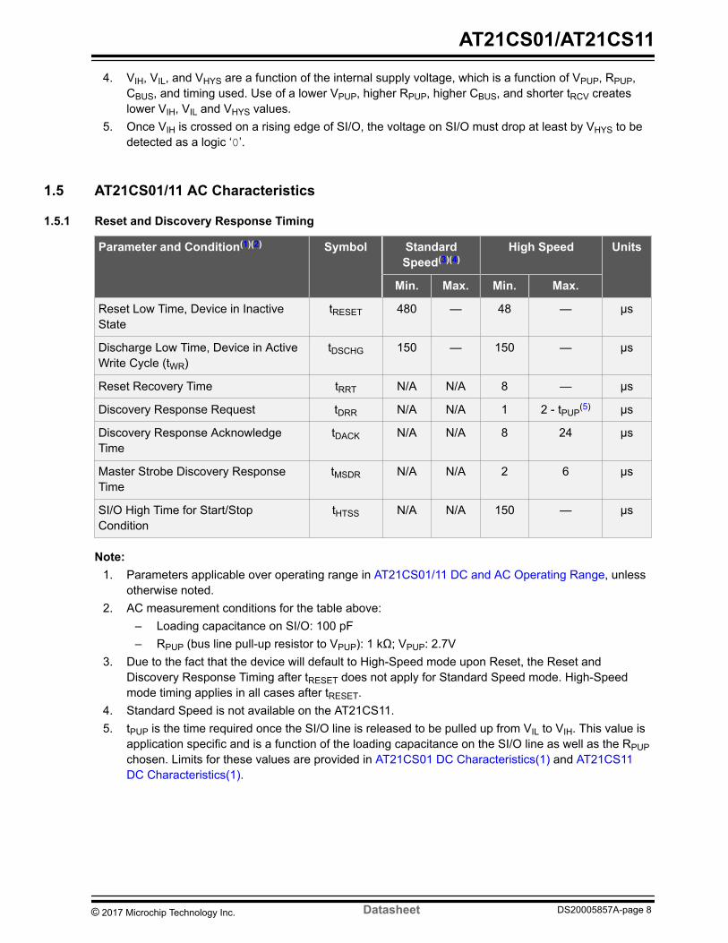
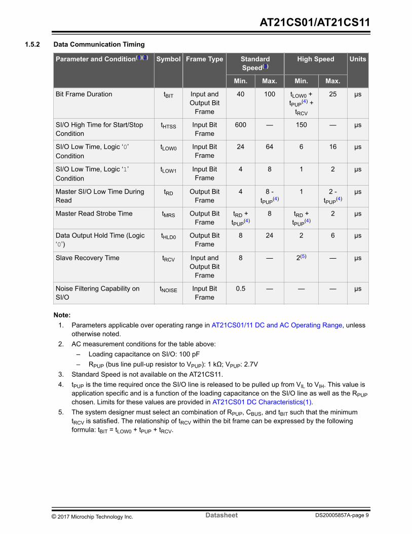
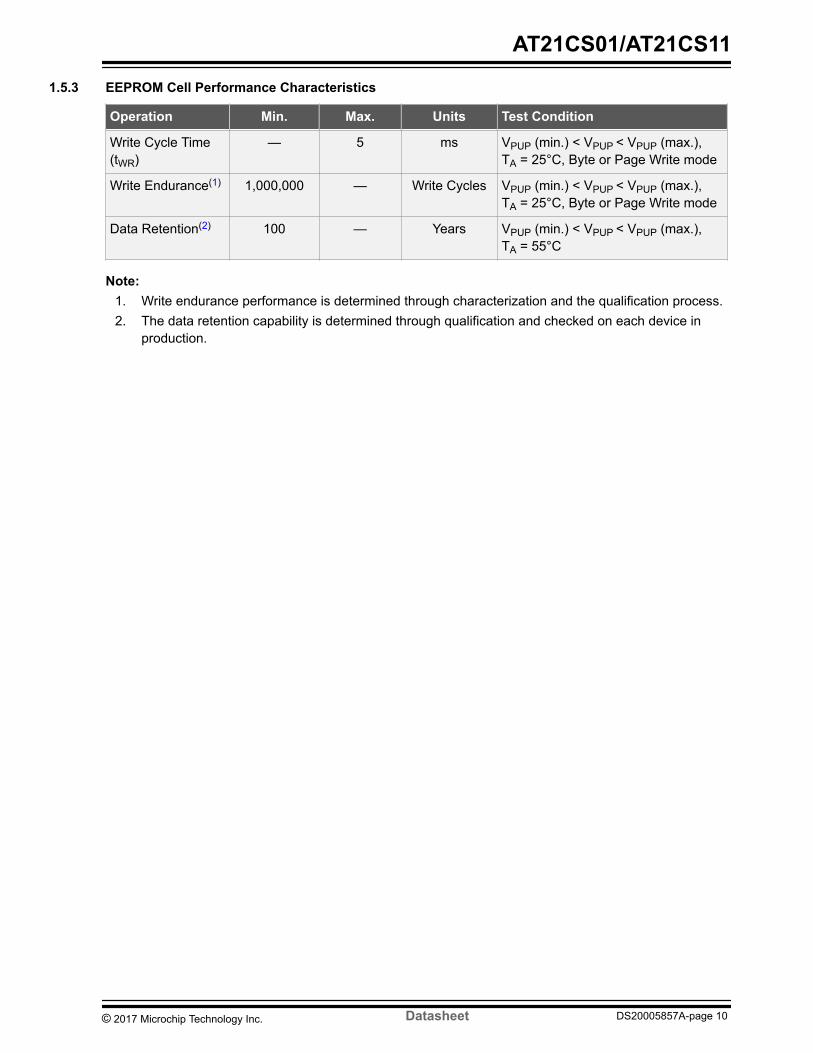
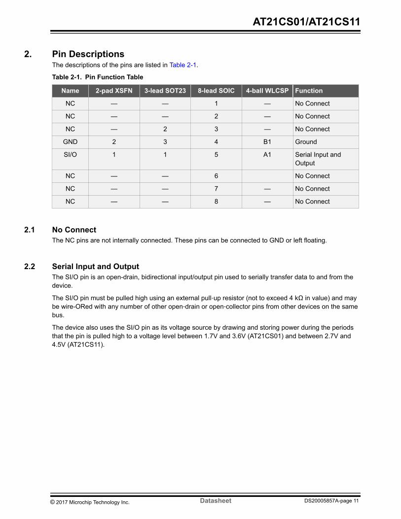
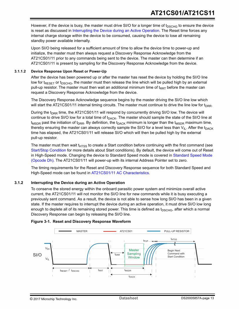
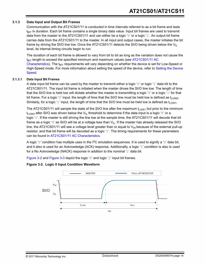
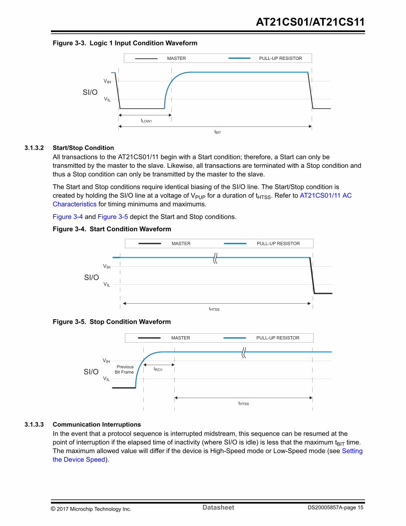
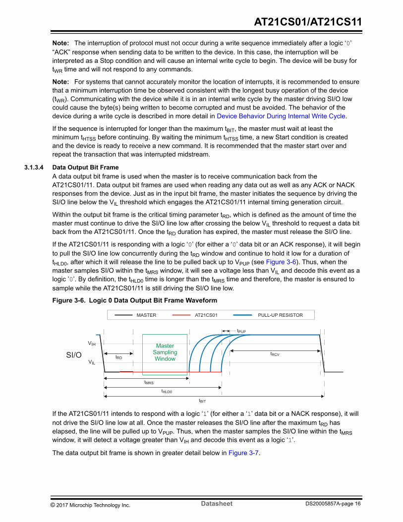

Figure 3-7 Logic 1 Data Output Bit Frame Waveform
AT21CS01 [DATASHEET]Atmel-8903A-SEEPROM-AT21CS01-Datasheet_082015
10
3134 Data Output Bit FrameA data output Bit Frame is used when the Master is to receive communication back from the AT21CS01 Data output Bit Frames are used when reading any data out as well as any ACK or NACK responses from the deviceJust as in the input Bit Frame the Master initiates the sequence by driving the SIO line below the VIL threshold which engages the AT21CS01rsquos internal timing generation circuit Within the output Bit Frame is the critical timing parameter tRD which is defined as the amount of time the Master must continue to drive the SIO line low after crossing the below VIL threshold to request a data bit back from the AT21CS01 Once the tRD duration has expired the Master must release the SIO line If the AT21CS01 is responding with a Logic 0 (for either a lsquo0rsquo data bit or an ACK response) it will begin to pull the SIO line low concurrently during the tRD window and continue to hold it low for a duration of tHLD0 after which it will release the line to be pulled back up to VPUP (see Figure 3-6) Thus when the Master samples SIO within the tMRS window it will see a voltage less than VIL and decode this event as a Logic 0 By definition the tHLD0 time is longer than the tMRS time and therefore the Master is guaranteed to sample while the AT21CS01 is still driving the SIO line low
Figure 3-6 Logic 0 Data Output Bit Frame Waveform
If the AT21CS01 intends to respond with a Logic 1 (for either a lsquo1rsquo data bit or a NACK response) it will not drive the SIO line low at all Once the Master releases the SIO line after the maximum tRD has elapsed the line will be pulled up to VPUP Thus when the Master samples the SIO line within the tMRS window it will detect a voltage greater than VIH and decode this event as a Logic 1The data output Bit Frame is shown in greater detail below in Figure 3-7
Figure 3-7 Logic 1 Data Output Bit Frame Waveform
SIOVIL
VIH
tBIT
MASTER PULL-UP RESISTOR
tMRS
tRCV
AT21CS01
MasterSamplingWindowtRD
tHLD0
tPUP
SIOVIL
VIH
tBIT
MASTER PULL-UP RESISTOR
tMRS
AT21CS01
MasterSamplingWindowtRD
tPUP
Note AT21CS01 will not drive the SIO line during a Logic 1 output Bit Frame
AT21CS01AT21CS11
copy 2017 Microchip Technology Inc Datasheet DS20005857A-page 17
4 Device Addressing and I2C Protocol EmulationAccessing the device requires a Start condition followed by an 8-bit device address word
The AT21CS0111 protocol sequence emulates what would be required for an I2C Serial EEPROM withthe exception that the beginning four bits of the device address are used as an opcode for the differentcommands and actions that the device can perform
Since multiple slave devices can reside on the bus each slave device must have its own unique addressso that the master can access each device independently After the 4-bit opcode the following three bitsof the device address byte are comprised of the slave address bits The three slave address bits arepreprogrammed prior to shipment and are read-only Obtaining devices with different slave address bitvalues is done by purchasing a specific ordering code Refer to Packaging Information for explanation ofwhich ordering code corresponds with a specific slave address value
Following the three slave address bits is a ReadWrite select bit where a logic lsquo1rsquo indicates a read and alogic lsquo0rsquo indicates a write Upon the successful comparison of the device address the EEPROM will returnan ACK (logic lsquo0rsquo) If the 4-bit opcode is invalid or the three bits of slave address do not match what ispreprogrammed in the device the device will not respond on the SIO line and will return to a Standbystate
Table 4-1 Device Address Byte
4-bit Opcode Preprogrammed Slave Address Bits ReadWrite
Bit 7 Bit 6 Bit 5 Bit 4 Bit 3 Bit 2 Bit 1 Bit 0
Refer to Available Opcodes A2 A1 A0 RW
Following the device address byte a memory address byte must be transmitted to the deviceimmediately The memory address byte contains a 7-bit memory array address to specify which locationin the EEPROM to start reading or writing Refer to Table 4-2 to review these bit positions
Table 4-2 Memory Address Byte
Bit 7 Bit 6 Bit 5 Bit 4 Bit 3 Bit 2 Bit 1 Bit 0
Donrsquot Care A6 A5 A4 A3 A2 A1 A0
41 Memory OrganizationThe AT21CS0111 internal memory array is partitioned into two regions The main 1-Kbit EEPROM isorganized as 16 pages of eight bytes each The Security register is 256 bits in length organized as fourpages of eight bytes each The lower two pages of the Security register are read-only and have afactory‑programmed 64‑bit serial number that is unique across all AT21CS series Serial EEPROMs Theupper two pages of the Security register are user-programmable and can be subsequently locked (see Locking the Security Register)
AT21CS01AT21CS11
copy 2017 Microchip Technology Inc Datasheet DS20005857A-page 18
Figure 4-1 Memory Architecture Diagram
Main1-Kbit
EEPROM
256-bitSecurityRegister
Zone 2
1-Kbit Address Range (00h-7Fh)
User-Programmable MemoryAddress Range (10h-1Fh)
64-bit Serial NumberAddress Range (00h-07h)
Permanently Lockableby Software
Opcode 1010b (Ah)
Opcode1011b (Bh)
Read-Only
Four 256-bit ROM Zones
Each can be independently
set to read-only
Zone 0
Zone 1
Zone 2
Zone 3
Reserved for Future UseAddress Range (08h-0Fh)
AT21CS01AT21CS11
copy 2017 Microchip Technology Inc Datasheet DS20005857A-page 19
5 Available OpcodesTable 5-1 outlines available opcodes for the AT21CS0111
Table 5-1 Opcodes used by the AT21CS0111
Command 4-Bit Opcode Brief Description of Functionality
EEPROM Access 1010 (Ah) ReadWrite the contents of the main memory array
Security Register Access 1011 (Bh) ReadWrite the contents of the Security register
Lock Security Register 0010 (2h) Permanently lock the contents of the Security register
ROM Zone RegisterAccess
0111 (7h) Inhibit further modification to a zone of the EEPROM array
Freeze ROM Zone State 0001 (1h) Permanently lock the current state of the ROM Zoneregisters
Manufacturer ID Read 1100 (Ch) Query manufacturer and density of device
Standard Speed Mode 1101 (Dh) Switch to Standard Speed mode operation (AT21CS01only command the AT21CS11 will NACK this command)
High-Speed Mode 1110 (Eh) Switch to High-Speed mode operation (AT21CS0111power‑on default AT21CS11 will ACK this command)
51 EEPROM Access (Opcode Ah)The opcode Ah is used to read data from and write data to the EEPROM Refer to Read Operations formore details about reading data from the device For details about writing to the EEPROM refer to WriteOperations
52 Security Register Access (Opcode Bh)The opcode Bh is used to read data from and write data to the Security register Refer to ReadOperations in the Security Register for more details about reading data from the Security register Fordetails about writing to the user-programmable portion of the Security register refer to section Writing tothe Security Register
53 Lock Security Register (Opcode 2h)The opcode 2h is used to permanently lock the user-programmable portion of the Security register Referto Locking the Security Register
54 ROM Zone Register Access (Opcode 7h)The AT21CS0111 is partitioned into four 256-bit zones each of which can be independently andpermanently made read-only (ROM) The state of each zone is stored in a Configuration register whichcan be read from or written to using the opcode 7h The ROM Zone functionality is explained in greaterdetail in ROM Zones
AT21CS01AT21CS11
copy 2017 Microchip Technology Inc Datasheet DS20005857A-page 20
55 Freeze ROM Zone State (Opcode 1h)The opcode 1h is used to permanently freeze the current state of the ROM Zone registers Once set theROM Zone registers are read-only
Therefore any zone that is not already read-only cannot be subsequently converted to ROM Refer to Freeze ROM Zone Registers for additional details
56 Manufacturer ID Read (Opcode Ch)Manufacturer identification device density and device revision information can be read from the deviceusing the opcode Ch The full details of the format of the data returned by this command are found in Manufacturer ID Read
57 Standard Speed Mode (Opcode Dh)The AT21CS01 can be set to Standard Speed mode or checked to see whether or not it is in StandardSpeed mode with the use of the Dh opcode Further details are covered in Standard Speed Mode(AT21CS01) The AT21CS11 does not offer Standard Speed mode and therefore will NACK thiscommand
58 High-Speed Mode (Opcode Eh)The AT21CS01 can be set to High-Speed mode or checked to see whether or not it is in High-Speedmode with the use of the Eh opcode The AT21CS11 only operates in High-Speed mode and thereforewill ACK this command Further details are covered in High-Speed Mode
AT21CS01AT21CS11
copy 2017 Microchip Technology Inc Datasheet DS20005857A-page 21
6 Write OperationsAll write operations for the AT21CS0111 begin with the master sending a Start condition followed by adevice address byte (opcode Ah for the EEPROM and opcode Bh for the Security register) with the RWbit set to lsquo0rsquo followed by the memory address byte Next the data value(s) to be written to the device aresent Data values must be sent in 8-bit increments to the device followed by a Stop condition If a Stopcondition is sent somewhere other than at the byte boundary the current write operation will be aborted
The AT21CS0111 allows single byte writes partial page writes and full page writes
61 Device Behavior During Internal Write CycleTo ensure that the address and data sent to the device for writing are not corrupted while any type ofinternal write operation is in progress commands sent to the device are blocked from being recognizeduntil the internal operation is completed If a write interruption occurs (SIO pulsed low) and is smallenough to not deplete the internal power storage the device will NACK signaling that the operation is inprogress If an interruption is longer than tDSCHG then internal write operation will be terminated and mayresult in data corruption
62 Byte WriteThe AT21CS0111 supports writing of a single 8-bit byte and requires a 7-bit memory word address toselect which byte to write
Upon receipt of the proper device address byte (with opcode of Ah) and memory address byte theEEPROM will send a logic lsquo0rsquo to signify an ACK The device will then be ready to receive the data byteFollowing receipt of the complete 8-bit data byte the EEPROM will respond with an ACK A Stopcondition must then occur however since a Stop condition is defined as a null bit frame with SIO pulledhigh the master does not need to drive the SIO line to accomplish this If a Stop condition is sent at anyother time the write operation is aborted After the Stop condition is complete the EEPROM will enter aninternally self-timed write cycle which will complete within a time of tWR while the data is beingprogrammed into the nonvolatile EEPROM The SIO pin must be pulled high via the external pull-upresistor during the entire tWR cycle After the maximum tWR time has elapsed the master may begin anew bus transactionNote
1 Any attempt to interrupt the internal write cycle by driving the SIO line low may cause the bytebeing programmed to be corrupted Other memory locations within the memory array will not beaffected Note Device Behavior During Internal Write Cycle for the behavior of the device while thewrite cycle is in progress If the master must interrupt a write operation the SIO line must be drivenlow for tDSCHG as noted in Interrupting the Device during an Active Operation
Figure 6-1 Byte Write
SIOMSB
ACKby Slave
1 0 1 0 A2 A1 A0 0
Device Address
MSB
x A6 A5 A4 A3 A2 A1 A0
Memory Address
MSB
D D D D D D D D
Data In Byte
ACKby Slave
`ACKby Slave
Stop Conditionby Master
Start Conditionby Master
0 0 0
Note 1 x = Donrsquot Care bit in the place of A7 as this bit falls outside the 1-Kbit addressable range
AT21CS01AT21CS11
copy 2017 Microchip Technology Inc Datasheet DS20005857A-page 22
63 Page WriteA page write operation allows up to eight bytes to be written in the same write cycle provided all bytesare in the same row (address bits A6 through A3 are the same) of the memory array Partial page writesof less than eight bytes are allowed
A page write is initiated the same way as a byte write but the bus master does not send a Stop conditionafter the first data byte is clocked in Instead after the EEPROM acknowledges receipt of the first databyte the bus master can transmit up to an additional seven data bytes
The EEPROM will respond with an ACK after each data byte is received Once all data bytes have beensent the device requires a Stop condition to begin the write cycle However since a Stop condition isdefined as a null bit frame with SIO pulled high the master does not need to drive the SIO line toaccomplish this If a Stop condition is sent at any other time the write operation is aborted After the Stopcondition is complete the internally self-timed write cycle will beginThe SIO pin must be pulled high viathe external pull-up resistor during the entire tWR cycle Thus in a multi‑slave environmentcommunication to other single-wire devices on the bus should not be attempted while any devices are inan internal write cycle
The lower three bits of the memory address are internally incremented following the receipt of each databyte The higher order address bits are not incremented and the device retains the memory pagelocation Page write operations are limited to writing bytes within a single physical page regardless of thenumber of bytes actually being written When the incremented word address reaches the page boundarythe address counter will ldquoroll overrdquo to the beginning of the same page Nevertheless creating a roll overevent should be avoided as previously loaded data in the page could become unintentionally alteredAfter the maximum tWR time has elapsed the master may begin a new bus transaction
Note 1 Any attempt to interrupt the internal write cycle by driving the SIO line low may cause the bytes
being programmed to be corrupted Other memory locations within the memory array will not beaffected Note Device Behavior During Internal Write Cycle for the behavior of the device while thewrite cycle is in progress If the master must interrupt a write operation the SIO line must be drivenlow for tDSCHG as noted in Interrupting the Device during an Active Operation
Figure 6-2 Page Write
SIOMSB
ACKby Slave
1 0 1 0 A2 A1 A0 0
Device Address
MSB
x A6 A5 A4 A3 A2 A1 A0
Memory Address
MSB
D D D D D D D D
Data In Byte (1)
D D D D D D D D
Data In Byte (8)
ACKby Slave
ACKby Slave
ACKby Slave
Stop Conditionby Master
Start Conditionby Master
0000
Note 1 x = Donrsquot Care bit in the place of A7 as this bit falls outside the 1-Kbit addressable range
64 Writing to the Security RegisterThe Security register supports bytes writes page writes and partial page writes in the upper 16 bytes(upper two pages of eight bytes each) of the region Page writes and partial page writes in the Securityregister have the same page boundary restrictions and behavior requirements as they do in theEEPROM
Upon receipt of the proper device address byte (with opcode of Bh specified) and memory address bytethe EEPROM will send a logic lsquo0rsquo to signify an ACK The device will then be ready to receive the first databyte
AT21CS01AT21CS11
copy 2017 Microchip Technology Inc Datasheet DS20005857A-page 23
Following receipt of the data byte the EEPROM will respond with an ACK and the master can send up toan additional seven bytes if desired The EEPROM will respond with an ACK after each data byte issuccessfully received Once all of the data bytes have been sent the device requires a Stop condition tobegin the write cycle However since a Stop condition is defined as a null bit frame with SIO pulled highthe master does not need to drive the SIO line to accomplish this After the Stop condition is completethe EEPROM will enter an internally self-timed write cycle which will complete within a time of tWR whilethe data is being programmed into the nonvolatile EEPROM The SIO pin must be pulled high via theexternal pull-up resistor during the entire tWR cycle Figure 6-3 is included below as an example of a bytewrite operation in the Security register
Figure 6-3 Byte Write in the Security Register
SIOMSB
ACKby Slave
1 0 1 1 A2 A1 A0 0
Device Address
MSB
x x x 1 A3 A2 A1 A0
MSB
D D D D D D D D
Data In Byte
ACKby Slave
ACKby Slave
Stop Conditionby Master
Start Conditionby Master
0 0 0
Security Register Address
Note 1 x = Donrsquot Care values in the place of A7‑A5 as these bits falls outside the addressable range of the
Security register2 Any attempt to interrupt the internal write cycle by driving the SIO line low may cause the byte
being programmed to be corrupted Other memory locations within the memory array will not beaffected Note Device Behavior During Internal Write Cycle for the behavior of the device while thewrite cycle is in progress If the master must interrupt a write operation the SIO line must be drivenlow for tDSCHG as noted in Interrupting the Device during an Active Operation
65 Locking the Security RegisterThe Lock command is an irreversible sequence that will permanently prevent all future writing to theupper 16 bytes of the Security register on the AT21CS0111 Once the Lock command has beenexecuted the entire 32-byte Security register becomes read-only Once the Security register has beenlocked it is not possible to unlock it
The Lock command protocol emulates a byte write operation to the Security register however theopcode 0010b (2h) is required along with the A7 through A4 bits of the memory address being set to0110b (6h) The remaining bits of the memory address as well as the data byte are donrsquot care bitsEven though these bits are donrsquot cares they still must be transmitted to the device An ACK response tothe memory address and data byte indicates the Security register is not currently locked A NACKresponse indicates the Security register is already locked Refer to Figure 6-5 for details aboutdetermining the Lock status of the Security register
The sequence completes with a Stop condition to initiate a self-timed internal write cycle If a Stopcondition is sent at any other time the Lock operation is aborted Since a Stop condition is defined as anull bit frame with SIO pulled high the master does not need to drive the SIO line to accomplish thisUpon completion of the write cycle (taking a time of tWR) the Lock operation is complete and the Securityregister will become permanently read-only
Note 1 Any attempt to drive the SIO line low during the tWR time period may cause the Lock operation to
not complete successfully and must be avoided
AT21CS01AT21CS11
copy 2017 Microchip Technology Inc Datasheet DS20005857A-page 24
Figure 6-4 Lock Command
SIOMSB
ACKby Slave
0 0 1 0 A2 A1 A0 0
Device Address
MSB
0 1 1 0 X X X X
Lock Security Register Address
MSB
X X X X X X X X
Data In Byte
ACKby Slave
ACKby Slave
Stop Conditionby Master
Start Conditionby Master
0 0 0
651 Device Response to a Write Command on a Locked DeviceA locked device will respond differently to a Write command to the Security register compared to a devicethat has not been locked Writing to the Security register is accomplished by sending a Start conditionfollowed by a device address byte with the opcode of 1011b (Bh) the appropriate slave addresscombination and the ReadWrite bit set as a logic lsquo0rsquo Both a locked device and a device that has notbeen locked will return an ACK Next the 8-bit word address is sent and again both devices will return anACK However upon sending the data input byte a device that has already been locked will return aNACK and be immediately ready to accept a new command whereas a device that has not been lockedwill return an ACK to the data input byte as per normal operation for a Write command as described in Write Operations
652 Check Lock CommandThe Check Lock command follows the same sequence as the Lock command (including 0110b in the A7through A4 bits of the memory address byte) with the exception that only the device address byte andmemory address byte need to be transmitted to the device An ACK response to the memory addressbyte indicates that the lock has not been set while a NACK response indicates that the lock has been setIf the lock has already been enabled it cannot be reversed The Check Lock command is completed bythe master sending a Stop bit to the device (defined as a null bit frame)
Figure 6-5 Check Lock Command
SIOMSB
ACKby Slave
0 0 1 0 A2 A1 A0 0
Device Address
MSB
0 1 1 0 X X X X
Lock Security Register Address
ACK by Slaveif Unlocked
NACK by Slaveif Locked
Stop Conditionby Master
Start Conditionby Master
0
66 Setting the Device SpeedThe AT21CS01 can be set to Standard Speed mode (154 kbps maximum) or High-Speed mode(125 kbps maximum) through a software sequence Upon executing a Reset and Discovery Responsesequence (see Device ResetPower-up and Discovery Response) the device will default to High-Speedmode The AT21CS11 does not have Standard Speed mode
661 Standard Speed Mode (AT21CS01)The AT21CS01 can be set to Standard Speed mode or checked to see whether or not it is in StandardSpeed mode with the use of the Dh opcode This transaction only requires eight bits
To set the device to Standard Speed mode the master must send a Start condition followed by thedevice address byte with the opcode of 1101b (Dh) specified along with the appropriate slave addresscombination and the ReadWrite bit set to a logic lsquo0rsquo The device will return an ACK (logic lsquo0rsquo) and will beimmediately ready to receive commands for standard speed operation
AT21CS01AT21CS11
copy 2017 Microchip Technology Inc Datasheet DS20005857A-page 25
To determine if the device is already set to Standard Speed mode the device address byte with theopcode of 1101b (Dh) must be sent to the device along with the appropriate slave address combinationand the ReadWrite bit set to a logic lsquo1rsquo The device will return an ACK (logic lsquo0rsquo) if it was set for StandardSpeed mode It will return a NACK (logic lsquo1rsquo) if the device was not currently set for Standard Speed mode
Note The AT21CS11 will NACK this command
662 High-Speed ModeThe device can be set to High-Speed mode or checked to see whether or not it is in High-Speed modewith the use of the Eh opcode This transaction only requires eight bits The power-on default for theAT21CS0111 is High-Speed mode
To set the device to High-Speed mode the master must send a Start condition followed by the deviceaddress byte with the opcode of 1110b (Eh) specified along the appropriate slave address combinationand the ReadWrite bit set to a logic lsquo0rsquo The device will return an ACK (Logic 0) and will be immediatelyready to receive commands for high-speed operation
To determine if the device is already set to High-Speed mode the device address byte with the opcode of1110b (Eh) specified must be sent to the device along with the appropriate slave address combinationand the ReadWrite bit set to a logic lsquo1rsquo The device will return an ACK (logic lsquo0rsquo) if it was set for High-Speed mode It will return a NACK (logic lsquo1rsquo) if the device was not currently set for High-Speed mode
Note The AT21CS11 will ACK this command
AT21CS01AT21CS11
copy 2017 Microchip Technology Inc Datasheet DS20005857A-page 26
7 Read OperationsRead operations are initiated in a similar way as write operations with the exception that the ReadWriteselect bit in the device address byte must be set to a logic lsquo1rsquo There are multiple read operationssupported by the device
bull Current Address Read within the EEPROMbull Random Read within the EEPROMbull Sequential Read within the EEPROMbull Read from the Security Registerbull Manufacturer ID Read
Note 1 The AT21CS0111 contains a single shared-memory Address Pointer that maintains the
address of the next byte in the EEPROM or Security register to be accessed For example ifthe last byte read or written was memory location 0Dh of the EEPROM then the AddressPointer will be pointing to memory location 0Eh of the EEPROM As such when changingfrom a read in one region to the other the first read operation in the new region should beginwith a random read instead of a current address read to ensure the Address Pointer is set toa known value within the desired region
If the end of the EEPROM or the Security register is reached then the Address Pointer will ldquoroll overrdquoback to the beginning (address 00h) of that region The Address Pointer retains its value betweenoperations as long as the pull-up voltage on the SIO pin is maintained or as long as the device has notbeen reset
71 Current Address Read within the EEPROMThe internal Address Pointer must be pointing to a memory location within the EEPROM in order toperform a current address read from the EEPROM To initiate the operation the master must send a Startcondition followed by the device address byte with the opcode of 1010b (Ah) specified along with theappropriate slave address combination and the ReadWrite bit set to a logic lsquo1rsquo After the device addressbyte has been sent the AT21CS0111 will return an ACK (logic lsquo0rsquo)
Following the ACK the device is ready to output one byte (eight bits) of data The master initiates the allbits of data by driving the SIO line low to start The AT21CS0111 will hold the line low after the masterreleases it to indicate a logic lsquo0rsquo If the data is logic lsquo1rsquo the AT21CS0111 will not hold the SIO line low atall causing it to be pulled high by the pull-up resistor once the master releases it This sequence repeatsfor eight bits
After the master has read the first data byte and no further data is desired the master must return aNACK (logic lsquo1rsquo) response to end the read operation and return the device to the Standby mode Figure7-1 depicts this sequence
If the master would like the subsequent byte it would return an ACK (logic lsquo0rsquo) and the device will beready output the next byte in the memory array Refer to Sequential Read within the EEPROM for detailsabout continuing to read beyond one byte
Note 1 If the last operation to the device was an access to the Security register then a random read should
be performed to ensure that the Address Pointer is set to a known memory location within theEEPROM
AT21CS01AT21CS11
copy 2017 Microchip Technology Inc Datasheet DS20005857A-page 27
Figure 7-1 Current Address Read
SIOMSB
ACKby Slave
1 0 1 0 A2 A1 A0 1
Device Address
MSB
D D D D D D D D
Data Out Byte (n)
NACK by Master
Stop Conditionby Master
Start Conditionby Master
0 1
72 Random Read within the EEPROMA random read begins in the same way as a byte write operation which will load a new EEPROM memoryaddress into the Address Pointer However instead of sending the data byte and Stop condition of thebyte write a repeated Start condition is sent to the device This sequence is referred to as a ldquodummywriterdquo After the device address and memory address bytes of the ldquodummy writerdquo have been sent theAT21CS0111 will return an ACK response The master can then initiate a current address readbeginning with a new Start condition to read data from the EEPROM Refer to Current Address Readwithin the EEPROM for details on how to perform a current address read
Figure 7-2 Random Read
SIOMSB
ACKby Slave
1 0 1 0 A2 A1 A0 0
Device Address
Dummy Write
MSB
x A6 A5 A4 A3 A2 A1 A0
Memory Address
MSB
D D D D D D D D
Data Out Byte (n)
ACKby Slave
NACKby Master
Stop Conditionby Master
Start Conditionby Master
MSB
ACKby Slave
1 0 1 0 A2 A1 A0 1
Device Address
Restartby Master
1000
73 Sequential Read within the EEPROMSequential reads start as either a current address read or as a random read However instead of themaster sending a NACK (logic lsquo1rsquo) response to end a read operation after a single byte of data has beenread the master sends an ACK (logic lsquo0rsquo) to instruct the AT21CS0111 to output another byte of data Aslong as the device receives an ACK from the master after each byte of data has been output it willcontinue to increment the address counter and output the next byte data from the EEPROM If the end ofthe EEPROM is reached then the Address Pointer will ldquoroll overrdquo back to the beginning (address 00h) ofthe EEPROM region To end the sequential read operation the master must send a NACK response afterthe device has output a complete byte of data After the device receives the NACK it will end the readoperation and return to the Standby mode
Note 1 If the last operation to the device accessed the Security register then a random read should be
performed to ensure that the Address Pointer is set to a known memory location within theEEPROM
Figure 7-3 Sequential Read from a Current Address Read
SIOMSB
ACKby Slave
1 0 1 0 A2 A1 A0 1
Device Address
MSB
D D D D D D D D
Data Out Byte (n)
ACK by Master
MSB
D D D D D D D D
Data Out Byte (n+x)
NACK by Master
Stop Conditonby Master
Start Conditionby Master
0 0 1
AT21CS01AT21CS11
copy 2017 Microchip Technology Inc Datasheet DS20005857A-page 28
Figure 7-4 Sequential Read from a Random Read
SIOMSB
ACKby Slave
1 0 1 0 A2 A1 A0 0
Device Address
MSB
x A6 A5 A4 A3 A2 A1 A0
Memory Address
MSB
D D D D D D D D
Data Out Byte (n)
ACKby Slave
ACKby Master
Stop Conditionby Master
Start Conditionby Master
MSB
ACKby Slave
1 0 1 0 A2 A1 A0 1
Device Address
Restartby Master
MSB
D D D D D D D D
Data Out Byte (n + x)
Dummy Write
NACK by Master
0 10
00
74 Read Operations in the Security RegisterThe Security register can be read by using either a random read or a sequential read operation Due tothe fact that the EEPROM and Security register share a single Address Pointer register a ldquodummy writerdquomust be performed to correctly set the Address Pointer in the Security register This is why a random reador sequential read must be used as these sequences include a ldquodummy writerdquo Bits A7 through A5 aredonrsquot care bits as these fall outside the addressable range of the Security register Current addressreads of the Security register are not supported
In order to read the Security register the device address byte must be specified with the opcode 1011b(Bh) instead of the opcode 1010b (Ah)The Security register can be read to read the 64-bit serial numberor the remaining user-programmable data
741 Serial Number ReadThe lower eight bytes of the Security register contain a factory-programmed unique 64‑bit serial numberIn order to ensure a unique value the entire 64-bit serial number must be read starting at Securityregister address location 00h Therefore it is recommended that a sequential read started with a randomread operation be used ensuring that the random read sequence uses a device address byte withopcode 1011b (Bh) specified in addition to the memory address byte being set to 00h
The first byte read out of the 64-bit serial number is the product identifier (A0h) Following the productidentifier a 48-bit unique number is contained in bytes 1 through 6 The last byte of the serial numbercontains a cyclic redundancy check (CRC) of the other 56 bits The CRC is generated using thepolynomial X8 + X5 + X4 + 1 The structure of the 64-bit serial number is depicted in Table 7-1
Table 7-1 64-Bit Factory-Programmed Serial Number Organization
Byte 0 Byte 1 Byte 2 Byte 3 Byte 4 Byte 5 Byte 6 Byte 7
8-bit ProductIdentifier
(A0h)
48-bit Unique Number 8-bit CRCValue
After all eight bytes of the serial number have been read the master can return a NACK (logic lsquo1rsquo)response to end the read operation and return the device to the Standby mode If the master sends anACK (logic lsquo0rsquo) instead of a NACK then the next byte (address location 08h) in the Security register willbe output If the end of the Security register is reached then the Address Pointer will ldquoroll overrdquo back tothe beginning (address location 00h) of the Security register
AT21CS01AT21CS11
copy 2017 Microchip Technology Inc Datasheet DS20005857A-page 29
Figure 7-5 Serial Number Read
SIOMSB
ACKby Slave
1 0 1 1 A2 A1 A0 0
Device Address
MSB
X X X 0 0 0 0 0
Serial Number Starting Address
MSB
D D D D D D D D
Serial Number Byte 00h
ACKby Slave
ACKby Master
Stop Conditionby Master
Start Conditionby Master
MSB
ACKby Slave
1 0 1 1 A2 A1 A0 1
Device Address
Restartby Master
MSB
D D D D D D D D
Serial Number Byte 07h
Dummy Write
NACK by Master
0 10
00
75 Manufacturer ID ReadThe AT21CS0111 offers the ability to query the device for manufacturer density and revisioninformation By using a specific opcode and following the format of a current address read the device willreturn a 24-bit value that corresponds with the I2C identifier value reserved for Microchip along withfurther data to signify a 1-Kbit density and the device revision
To read the Manufacturer ID data the master must send a Start condition followed by the device addressbyte with the opcode of 1100b (Ch) specified along the appropriate slave address combination and theReadWrite bit set to a logic lsquo1rsquo After the device address byte has been sent the AT21CS0111 will returnan ACK (logic lsquo0rsquo) If the ReadWrite bit is set to a logic lsquo0rsquo to indicate a write the device will NACK (logiclsquo1rsquo) since the Manufacturer ID data is read-only
After the device has returned an ACK it will then send the first byte of Manufacturer ID data whichcontains the eight Most Significant bits (D23‑D16) of the 24-bit data value The master can then return anACK (logic lsquo0rsquo) to indicate it successfully received the data upon which the device will send the secondbyte (D15‑D8) of Manufacturer ID data The process repeats until all three bytes have been read out andthe master sends a NACK (logic lsquo1rsquo) to complete the sequence Figure 7-6 depicts this sequence below Ifthe master ACKs (logic lsquo0rsquo) the third byte the Internal Pointer will roll over back to the first byte ofManufacturer ID data
Figure 7-6 Manufacturer ID Read
SIOMSB
ACKby Slave
1 1 0 0 A2 A1 A0 1
Device Address
MSB(D23)
D D D D D D D D
Manufacturer ID Byte 1
ACK by Master
D D D D D D D D
Manufacturer ID Byte 2
NACK by Master
Stop Conditionby Master
Start Conditionby Master
ACK by Master
LSB(D0)
D D D D D D D D
Manufacturer ID Byte 3
0 100
Table 7-2 below provides the format of the Manufacturer ID data
Table 7-2 Manufacturer ID Data Format
Device Manufacturer CodeltD23D12gt
Device CodeltD11D3gt
Revision CodeltD2D0gt
Hex ValueltD23D0gt
AT21CS01 0000-0000-1101 0010-0000-0 000 00D200h
AT21CS11 0000-0000-1101 0011-1000-0 000 00D380h
AT21CS01AT21CS11
copy 2017 Microchip Technology Inc Datasheet DS20005857A-page 30
The Manufacturer Identifier portion of the ID is returned in the 12 Most Significant bits of the three bytesread out The value reserved for Microchip is 0000-0000-1101b (00Dh) Therefore the first byte readout by the device will be 00h The upper nibble of the second byte read out is Dh
The Least Significant 12 bits of the 24-bit ID is comprised of a Microchip defined value that indicates thedevice density and revision Bits D11 through D3 indicate the device code and bits D2 through D0indicate the device revision The output is shown more specifically in Table 7-2
The overall 24-bit value returned by the AT21CS01 is 00D200h The overall 24‑bit value returned by theAT21CS11 is 00D380h
AT21CS01AT21CS11
copy 2017 Microchip Technology Inc Datasheet DS20005857A-page 31
8 ROM Zones
81 ROM Zone Size and ROM Zone RegistersCertain applications require that portions of the EEPROM memory array be permanently protectedagainst malicious attempts at altering program code data modules security information orencryptiondecryption algorithms keys and routines To address these applications the memory array issegmented into four different memory zones of 256 bits each A ROM Zone mechanism has beenincorporated that allows any combination of individual memory zones to be permanently locked so thatthey become read‑only (ROM) Once a memory zone has been converted to ROM it can never beerased or programmed again and it can never be unlocked from the ROM state Table 8-2 shows theaddress range of each of the four memory zones
811 ROM Zone RegistersEach 256-bit memory zone has a corresponding single-bit ROM Zone register that is used to control theROM status of that zone These registers are nonvolatile and will retain their state even after a devicepower cycle or Reset operation The following table outlines the two states of the ROM Zone registersEach ROM Zone register has specific ROM Zone register address that is reserved for read or writeaccess
Table 8-1 ROM Zone Register Values
Value ROM Zone Status
0 ROM Zone is not enabled and that memory zone can be programmed and erased (the defaultstate)
1 ROM Zone is enabled and that memory zone can never be programmed or erased again
Issuing the ROM Zone command to a particular ROM Zone register address will set the correspondingROM Zone register to the logic lsquo1rsquo state Each ROM Zone register can only be set once therefore onceset to the logic lsquo1rsquo state a ROM Zone cannot be reset back to the logic lsquo0rsquo state
Table 8-2 ROM Zone Address Ranges
Memory Zone Starting Memory Address Ending Memory Address ROM Zone Register Address
0 0h 1Fh 01h
1 20h 3Fh 02h
2 40h 5Fh 04h
3 60h 7Fh 08h
82 Programming and Reading the ROM Zone Registers
821 Reading the Status of a ROM Zone RegisterTo check the current status of a ROM Zone register the master must emulate a random read sequencewith the exception that the opcode 0111b (7h) will be used The dummy write portion of the random readsequence is needed to specify which ROM Zone register address is to be read
AT21CS01AT21CS11
copy 2017 Microchip Technology Inc Datasheet DS20005857A-page 32
This sequence begins by the master sending a Start condition followed by a device address byte with theopcode of 7h in the four Most Significant bits along with the appropriate slave address combination andthe ReadWrite bit set to a logic lsquo0rsquo The AT21CS0111 will respond with an ACK
Following this device address byte is an 8-bit ROM Zone register address byte The four Most Significantbits are not used and are therefore donrsquot care bits The address sent to the device must match one ofthe ROM Zone register addresses specified in Table 8-3 After the ROM Zone register address has beensent the AT21CS0111 will return an ACK (logic lsquo0rsquo)
Then an additional Start condition is sent to the device with the same device address byte as before butnow with the ReadWrite bit set to a logic lsquo1rsquo to which the device will return an ACK After theAT21CS0111 has sent the ACK the device will output either 00h or FFh data byte A 00h data byteindicates that the ROM Zone register is zero meaning the zone has not been set as ROM If the deviceoutputs FFh data then the memory zone has been set to ROM and cannot be altered
Table 8-3 Read ROM Zone Register ndash Output Data
Output Data ROM Zone Register Value
00h ROM Zone register value is zero (zone is not set as ROM)
FFh ROM Zone register value is one (zone is permanently set as ROM)
Figure 8-1 Reading the State of a ROM Zone Register
SIOMSB
ACKby Slave
0 1 1 1 A2 A1 A0 0
Device Address
Dummy Write
MSB
0 0 0 0 A3 A2 A1 A0
ROM Zone Register Address
MSB
D D D D D D D D
Data Out Byte (00h or FFh)
ACKby Slave
NACKby Master
Stop Conditionby Master
Start Conditionby Master
MSB
ACKby Slave
0 1 1 1 A2 A1 A0 1
Device Address
Restartby Master
1000
822 Writing to a ROM Zone RegisterA ROM Zone register can only be written to a logic lsquo1rsquo which will set the corresponding memory zone to aROM state Once a ROM Zone register has been written it can never be altered again
To write to a ROM Zone register the master must send a Start condition followed by the device addressbyte with the opcode of 0111b (7h) specified along with the appropriate slave address combination andthe ReadWrite bit set to a logic lsquo0rsquo The device will return an ACK After the device address byte hasbeen sent the AT21CS0111 will return an ACK
Following the device address byte is an 8-bit ROM Zone register address byte The address sent to thedevice must match one of the ROM Zone register addresses specified in Table 8-2 After the ROM Zoneregister address has been sent the AT21CS0111 will return an ACK
After the AT21CS0111 has sent the ACK the master must send an FFh data byte in order to set theappropriate ROM Zone register to the logic lsquo1rsquo state The device will then return an ACK and after a Stopcondition is executed the device will enter a self-time internal write cycle lasting tWR If a Stop conditionis sent at any other point in the sequence the write operation to the ROM Zone register is aborted Thedevice will not respond till any commands until the tWR time has completed This sequence is depicted in Figure 8-2
AT21CS01AT21CS11
copy 2017 Microchip Technology Inc Datasheet DS20005857A-page 33
Figure 8-2 Writing to a ROM Zone Register
SIOMSB
ACKby Slave
0 1 1 1 A2 A1 A0 0
Device Address
MSB
0 0 0 0 A3 A2 A1 A0
ROM Zone Register Address
MSB
1 1 1 1 1 1 1 1
Data In Byte (FFh)
ACKby Slave
ACKby Slave
Stop Conditionby Master
Start Conditionby Master
0 0 0
Note 1 Any attempt to interrupt the internal write cycle by driving the SIO line low may cause the register
being programmed to become corrupted Note Device Behavior During Internal Write Cycle for thebehavior of the device while a write cycle is in progress If the master must interrupt a writeoperation the SIO line must be driven low for tDSCHG as noted in Interrupting the Device during anActive Operation
823 Freeze ROM Zone RegistersThe current ROM Zone state can be frozen so that no further modifications to the ROM Zone registerscan be made Once frozen this event cannot be reversed
To freeze the state of the ROM Zone registers the master must send a Start condition followed by thedevice address byte with the opcode of 0001b (1h) specified along with the appropriate slave addresscombination and the ReadWrite bit set to a logic lsquo0rsquo The device will return either an ACK (logic lsquo0rsquo)response if the ROM Zone registers have not been previously frozen or a NACK (logic lsquo1rsquo) response if theregisters have already been frozen
If the AT21CS0111 returns an ACK the master must send a fixed arbitrary address byte value of 55h towhich the device will return an ACK (logic lsquo0rsquo) Following the 55h address byte a data byte of AAh mustbe sent by the master The device will ACK after the AAh data byte If an address byte other than 55h ora data byte other than AAh is sent the device will NACK (logic lsquo1rsquo) and the freeze operation will not beperformed
To complete the Freeze ROM Zone register sequence a Stop condition is required If a Stop condition issent at any other point in this sequence the operation is aborted Since a Stop condition is defined as anull bit frame with SIO pulled high the master does not need to drive the SIO line to accomplish thisAfter the Stop condition is complete the internally self-timed write cycle will beginThe SIO pin must bepulled high via the external pull-up resistor during the entire tWR cycle
Figure 8-3 Freezing the ROM Zone Registers
SIOMSB
ACKby Slave
0 0 0 1 A2 A1 A0 0
Device Address
MSB
0 1 0 1 0 1 0 1
Fixed Abitrary Address (55h)
MSB
1 0 1 0 1 0 1 0
Data In Byte (AAh)
ACKby Slave
ACKby Slave
Stop Conditionby Master
Start Conditionby Master
0 0 0
Note 1 Any attempt to drive the SIO line low during the tWR time period may cause the Freeze operation to
not complete successfully and must be avoided
83 Device Response to a Write Command Within an Enabled ROM ZoneThe AT21CS0111 will respond differently to a Write command in a memory zone that has been set toROM compared to Write command in a memory zone that has not been set to ROM Writing to theEEPROM is accomplished by sending a Start condition followed by a device address byte with the
AT21CS01AT21CS11
copy 2017 Microchip Technology Inc Datasheet DS20005857A-page 34
opcode of 1010b (Ah) the appropriate slave address combination and the ReadWrite bit set as alogic lsquo0rsquo Since a memory address has not been input at this point in the sequence the device returns anACK Next the 8‑bit word address is sent which will result in an ACK from the device regardless if thataddress is in a memory zone that has been set to ROM However upon sending the data input byte aWrite command to an address that was in a memory zone that was set to ROM will result in a NACKresponse from the AT21CS0111 and the device will be immediately ready to accept a new command Ifthe address being written was in a memory zone that had not been set to ROM the device will return anACK to the data input byte as per normal operation for write operations as described in Write Operations
AT21CS01AT21CS11
copy 2017 Microchip Technology Inc Datasheet DS20005857A-page 35
9 Device Default Condition from MicrochipThe AT21CS0111 is delivered with the EEPROM array set to logic lsquo1rsquo state resulting in FFh data in alllocations
AT21CS01AT21CS11
copy 2017 Microchip Technology Inc Datasheet DS20005857A-page 36
10 Packaging Information
101 Package Marking Information
DRAWING NO REV TITLE
21CS0111SM A
91117
AT21CS0111SM AT21CS01 and AT21CS11 Package Marking Information
YYWWNNN COATMLHYWW
8-lead SOIC
Note 2 Package drawings are not to scale
Note 1 designates pin 1
AT21CS01AT21CS11 Package Marking Information
Diagram Order EIAJ PDIP SOICTSSOP UDFN SOT23VFBGAXDFN
Catalog Number TruncationAT21CS01 AT21CS11
Truncation Code K1M Truncation Code K2
Date Codes Slave AddressY = Year M = Month WW = Work Week of Assembly = Slave Address 7 2017 1 2021 A January 02 Week 2 A Address 000 E Address 1008 2018 2 2022 B February 04 Week 4 B Address 001 F Address 101 9 2019 3 2023 C Address 010 G Address 110 0 2020 4 2024 L December 52 Week 52 D Address 011 H Address 111
Country of Assembly Trace Code Atmel Truncation CO = Country of Assembly NNN or NN AT Atmel
ATM Atmel ATML Atmel
l
WWNNN
3-lead SOT-23
NN
4-ball WLCSP
ATMLYWWNNN
2-ld XSFN
(AT21CS01 only)
AT21CS01AT21CS11
copy 2017 Microchip Technology Inc Datasheet DS20005857A-page 37
DRAWING NO REV TITLE GPC
2MS-1 B
101414
2MS-1 2-pad 50x35 mm Body 040 thick Extra Thin Single Flat No Lead Package (XSFN) YDR
COMMON DIMENSIONS(Unit of Measure = mm)
SYMBOL MIN TYP MAX NOTE
A 030 035 040
A1 000 0035 005
A3 0127 REF
b 105 110 115 3
L 455 460 465
D 500 BSC
E 350 BSC
e 200 BSC
0 0deg - - 2
K 090 REF
Notes
1 Dimensioning and tolerancing conform to ASME Y145M - 1994
2 All dimensions are in millimeters 0 is in degrees
3 Dimension lsquobrsquo applies to metallized terminal and is measured between 015 and 030mm from terminal tip If the terminal has the optional radius on the
other end of the terminal the dimension lsquobrsquo should not be measured in that radius area
4 Maximum package warpage is 005mm
5 Maximum allowable burrs is 0076mm in all directions
6 Pin 1 on top will be laser marked
7 Unilateral coplanarity zone applies to the exposed heat sink slug as well as the terminals
010 m C A Bv 005 C 3
6
TOP VIEW BOTTOM VIEW
(DATUM A)
B
Ak 010 C
4XPin1 Corner
(DATUM B)1
2
A1
SEATING PLANE
A3 C
SIDE VIEW
1
2
D
E
A
7
0
C060 X 45deg
e
bL
0200
0200
K
7
Pin1 Corner
mk 0050 C
h 010 C
Note For the most current package drawings please see the Microchip Packaging Specification locatedat httpwwwmicrochipcompackaging
AT21CS01AT21CS11
copy 2017 Microchip Technology Inc Datasheet DS20005857A-page 38
AT21CS01 [DATASHEET]Atmel-8903A-SEEPROM-AT21CS01-Datasheet_082015
34
122 3ST1 mdash 3-lead SOT23
TITLE DRAWING NOGPC REV 3TS1
121109
COMMON DIMENSIONS(Unit of Measure = mm)
SYMBOL MIN NOM MAX NOTE
End View
Side View
Top View
3TS1 3-lead 130mm Body Plastic ThinShrink Small Outline Package (Shrink SOT)
BTBG
089001088280210120
030
AA1A2DEE1L1e1b
---
290-
130054 REF190 BSC
-
112010102304264140
050
12
12
3
Notes 1 Dimension D does not include mold flash protrusions or gate burrs Mold flash protrusions or gate burrs shall not exceed 025mm per end Dimension E1 does not include interlead flash or protrusion Interlead flash or protrusion shall not exceed 025mm per side
2 The package top may be smaller than the package bottomDimensions D and E1 are determined at the outermost extremes of the plastic body exclusive of mold flash tie bar burrs gate burrs and interlead flash but including any mismatch between the top and bottom of the plastic body
3 These dimensions apply to the flat section of the lead between008 mm and 015mm from the lead tip
This drawing is for general information only Refer to JEDEC Drawing TO-236 Variation AB for additional information
C L
L1
3
EE1
1 2e1
SEATINGPLANE
b
A2 A
A1e
D
GND
SDA VCC
Note For the most current package drawings please see the Microchip Packaging Specification locatedat httpwwwmicrochipcompackaging
AT21CS01AT21CS11
copy 2017 Microchip Technology Inc Datasheet DS20005857A-page 39
33AT21CS01 [DATASHEET]Atmel-8903A-SEEPROM-AT21CS01-Datasheet_082015
12 Packaging Information
121 8S1 mdash 8-lead SOIC
DRAWING NO REV TITLE GPC
COMMON DIMENSIONS(Unit of Measure = mm)
SYMBOL MIN NOM MAX NOTE
A1 010 ndash 025 A ndash ndash 175
b 031 ndash 051 C 017 ndash 025 D 490 BSC E 600 BSC E1 390 BSC
e 127 BSC L 040 ndash 127 OslashOslash 0deg ndash 8deg
Oslash
E
1
N
TOP VIEW
C
E1
END VIEW
Ab
L
A1
e
D
SIDE VIEW
8S1 H
362015
Notes This drawing is for general information onlyRefer to JEDEC Drawing MS-012 Variation AAfor proper dimensions tolerances datums etc
8S1 8-lead (0150rdquo Wide Body) Plastic Gull Wing Small Outline (JEDEC SOIC) SWB
Note For the most current package drawings please see the Microchip Packaging Specification locatedat httpwwwmicrochipcompackaging
AT21CS01AT21CS11
copy 2017 Microchip Technology Inc Datasheet DS20005857A-page 40
35AT21CS01 [DATASHEET]Atmel-8903A-SEEPROM-AT21CS01-Datasheet_082015
123 4U-6 mdash 4-ball WLCSP
DRAWING NO REV TITLE GPC
4U-6 B
8715
4U-6 4-ball 2x2 Array 040mm PitchWafer Level Chip-Scale Package (WLCSP) with BSC GPH
COMMON DIMENSIONS(Unit of Measure = mm)
SYMBOL MIN TYP MAX NOTEA 0313 0334 0355
A1 mdash 0094 mdash
A2 mdash 0240 mdash 3
D Contact Microchip for details
d1 0400 BSC
E Contact Microchip for details
e1 0400 BSC
b 0170 0185 0200
PIN ASSIGNMENT MATRIX
1 2
A
B
SIO
GND
NC
NC
TOP VIEW
SIDE VIEW
BOTTOM SIDE
Note 1 Dimensions are NOT to scale2 Solder ball composition is 955Sn-40Ag-05Cu3 Product offered with Back Side Coating
k 0015 (4X)
A
B
Ck 0075 C
SEATING PLANE
d b
A1 CORNERA1 CORNER
d 0015 m Cv 005 C A Bmd
D
E
d1
e1
A2A1
A
A
B
12
B
A
1 2
Note For the most current package drawings please see the Microchip Packaging Specification locatedat httpwwwmicrochipcompackaging
AT21CS01AT21CS11
copy 2017 Microchip Technology Inc Datasheet DS20005857A-page 41
11 Revision History
Atmel AT21CS01 Document 8903 Revision A (August 2015)Initial document release
Atmel AT21CS11 Document 8975 Revision A (August 2015)Initial document release Preliminary Status
Atmel AT21CS11 Document 8975 Revision B (November 2015)Removed Standard Speed mode
Revision A (October 2017)Updated to Microchip template This replaces Atmel documents 8903 and 8975 Added XSFN packageUpdated DC output current absolute maximum rating Removed lead finish designation Updated tracecode format in package markings
AT21CS01AT21CS11
copy 2017 Microchip Technology Inc Datasheet DS20005857A-page 42
The Microchip Web Site
Microchip provides online support via our web site at httpwwwmicrochipcom This web site is used asa means to make files and information easily available to customers Accessible by using your favoriteInternet browser the web site contains the following information
bull Product Support ndash Data sheets and errata application notes and sample programs designresources userrsquos guides and hardware support documents latest software releases and archivedsoftware
bull General Technical Support ndash Frequently Asked Questions (FAQ) technical support requestsonline discussion groups Microchip consultant program member listing
bull Business of Microchip ndash Product selector and ordering guides latest Microchip press releaseslisting of seminars and events listings of Microchip sales offices distributors and factoryrepresentatives
Customer Change Notification Service
Microchiprsquos customer notification service helps keep customers current on Microchip productsSubscribers will receive e-mail notification whenever there are changes updates revisions or erratarelated to a specified product family or development tool of interest
To register access the Microchip web site at httpwwwmicrochipcom Under ldquoSupportrdquo click onldquoCustomer Change Notificationrdquo and follow the registration instructions
Customer Support
Users of Microchip products can receive assistance through several channels
bull Distributor or Representativebull Local Sales Officebull Field Application Engineer (FAE)bull Technical Support
Customers should contact their distributor representative or Field Application Engineer (FAE) for supportLocal sales offices are also available to help customers A listing of sales offices and locations is includedin the back of this document
Technical support is available through the web site at httpwwwmicrochipcomsupport
AT21CS01AT21CS11
copy 2017 Microchip Technology Inc Datasheet DS20005857A-page 43
Product Identification System
To order or obtain information eg on pricing or delivery refer to the factory or the listed sales office
Tape and Reel Option
PART NO XX X XDevice Package Device
GradeOperating Voltage
ProductVariation
XX X[1]
Device AT21CS0111 Single-Wire IO Powered 1‑Kbit (128 x 8) Serial EEPROMwith Unique Factory‑Programmed 64‑bit Serial Number
Package Option MS = 2-Pad XSFN
ST = 3-Lead SOT23
SS = 8-Lead SOIC
U = 4-Ball WLCSP (AT21CS01 only)
WWU = Wafer Unsawn
Package Device Grade orWaferDie Thickness
H = Green Industrial Temperature Range (-40degC to +85degC)
U = Green Industrial Temperature Range (‑40degC to +85degC)
11 = 11 mil Wafer Thickness
Operating Voltage M = 17V to 36V (AT21CS01)
blank = 27V to 45V (AT21CS11)
Product Variation 10 = 0-0-0 Slave Address (A2 A1 A0)(2)
0B = 0-0-0 Slave Address (A2 A1 A0) WLCSP package with BackSide Coating
Tape and Reel Option B = Standard packaging (tube or tray)
T = Tape and Reel(1)
Note 1 Tape and Reel identifier only appears in the catalog part number description This identifier is used
for ordering purposes and is not printed on the device package Check with your Microchip SalesOffice for package availability with the Tape and Reel option
2 Please contact Microchip Sales to order devices with non 0-0-0 slave addresses
Examplesbull AT21CS01-SSHM10-T 17V-36V Industrial Temp Tape and Reel SOIC package
Slave Address 0-0-0bull AT21CS01-SSHM11-B 17V-36V Industrial Temp SOIC package Slave Address 0-0-1(2)
bull AT21CS01-MSHM15-T 17V-36V Industrial Temp Tape and Reel XSFN packageSlave Address 1-0-1(2)
bull AT21CS01-UUM0B-T 17V-36V Industrial Temp Tape and Reel UDFN packageSlave Address 0-0-0
AT21CS01AT21CS11
copy 2017 Microchip Technology Inc Datasheet DS20005857A-page 44
bull AT21CS11-STU10 27V-45V Industrial Temp SOT23 package Slave Address 0-0-0bull AT21CS11-MSH17-T 27V-45V Industrial Temp XSFN package Slave Address 1-1-1(2)
bull AT21CS11-WWU11(1) 27V-45V Industrial Temp 11 mil Thick Wafer ThicknessSlave Address 0-0-0 all die
Note 1 Contact Microchip Sales for wafer sales2 Please contact Microchip Sales to order non 0-0-0 slave addressed devices
Microchip Devices Code Protection Feature
Note the following details of the code protection feature on Microchip devices
bull Microchip products meet the specification contained in their particular Microchip Data Sheetbull Microchip believes that its family of products is one of the most secure families of its kind on the
market today when used in the intended manner and under normal conditionsbull There are dishonest and possibly illegal methods used to breach the code protection feature All of
these methods to our knowledge require using the Microchip products in a manner outside theoperating specifications contained in Microchiprsquos Data Sheets Most likely the person doing so isengaged in theft of intellectual property
bull Microchip is willing to work with the customer who is concerned about the integrity of their codebull Neither Microchip nor any other semiconductor manufacturer can guarantee the security of their
code Code protection does not mean that we are guaranteeing the product as ldquounbreakablerdquo
Code protection is constantly evolving We at Microchip are committed to continuously improving thecode protection features of our products Attempts to break Microchiprsquos code protection feature may be aviolation of the Digital Millennium Copyright Act If such acts allow unauthorized access to your softwareor other copyrighted work you may have a right to sue for relief under that Act
Legal Notice
Information contained in this publication regarding device applications and the like is provided only foryour convenience and may be superseded by updates It is your responsibility to ensure that yourapplication meets with your specifications MICROCHIP MAKES NO REPRESENTATIONS ORWARRANTIES OF ANY KIND WHETHER EXPRESS OR IMPLIED WRITTEN OR ORAL STATUTORYOR OTHERWISE RELATED TO THE INFORMATION INCLUDING BUT NOT LIMITED TO ITSCONDITION QUALITY PERFORMANCE MERCHANTABILITY OR FITNESS FOR PURPOSEMicrochip disclaims all liability arising from this information and its use Use of Microchip devices in lifesupport andor safety applications is entirely at the buyerrsquos risk and the buyer agrees to defendindemnify and hold harmless Microchip from any and all damages claims suits or expenses resultingfrom such use No licenses are conveyed implicitly or otherwise under any Microchip intellectualproperty rights unless otherwise stated
Trademarks
The Microchip name and logo the Microchip logo AnyRate AVR AVR logo AVR Freaks BeaconThingsBitCloud CryptoMemory CryptoRF dsPIC FlashFlex flexPWR Heldo JukeBlox KeeLoq KeeLoq logoKleer LANCheck LINK MD maXStylus maXTouch MediaLB megaAVR MOST MOST logo MPLABOptoLyzer PIC picoPower PICSTART PIC32 logo Prochip Designer QTouch RightTouch SAM-BA
AT21CS01AT21CS11
copy 2017 Microchip Technology Inc Datasheet DS20005857A-page 45
SpyNIC SST SST Logo SuperFlash tinyAVR UNIO and XMEGA are registered trademarks ofMicrochip Technology Incorporated in the USA and other countries
ClockWorks The Embedded Control Solutions Company EtherSynch Hyper Speed Control HyperLightLoad IntelliMOS mTouch Precision Edge and Quiet-Wire are registered trademarks of MicrochipTechnology Incorporated in the USA
Adjacent Key Suppression AKS Analog-for-the-Digital Age Any Capacitor AnyIn AnyOut BodyComchipKIT chipKIT logo CodeGuard CryptoAuthentication CryptoCompanion CryptoControllerdsPICDEM dsPICDEMnet Dynamic Average Matching DAM ECAN EtherGREEN In-Circuit SerialProgramming ICSP Inter-Chip Connectivity JitterBlocker KleerNet KleerNet logo Mindi MiWimotorBench MPASM MPF MPLAB Certified logo MPLIB MPLINK MultiTRAK NetDetach OmniscientCode Generation PICDEM PICDEMnet PICkit PICtail PureSilicon QMatrix RightTouch logo REALICE Ripple Blocker SAM-ICE Serial Quad IO SMART-IS SQI SuperSwitcher SuperSwitcher II TotalEndurance TSHARC USBCheck VariSense ViewSpan WiperLock Wireless DNA and ZENA aretrademarks of Microchip Technology Incorporated in the USA and other countries
SQTP is a service mark of Microchip Technology Incorporated in the USA
Silicon Storage Technology is a registered trademark of Microchip Technology Inc in other countries
GestIC is a registered trademark of Microchip Technology Germany II GmbH amp Co KG a subsidiary ofMicrochip Technology Inc in other countries
All other trademarks mentioned herein are property of their respective companiescopy 2017 Microchip Technology Incorporated Printed in the USA All Rights Reserved
ISBN 978-1-5224-2232-7
Quality Management System Certified by DNV
ISOTS 16949Microchip received ISOTS-169492009 certification for its worldwide headquarters design and waferfabrication facilities in Chandler and Tempe Arizona Gresham Oregon and design centers in Californiaand India The Companyrsquos quality system processes and procedures are for its PICreg MCUs and dsPICreg
DSCs KEELOQreg code hopping devices Serial EEPROMs microperipherals nonvolatile memory andanalog products In addition Microchiprsquos quality system for the design and manufacture of developmentsystems is ISO 90012000 certified
AT21CS01AT21CS11
copy 2017 Microchip Technology Inc Datasheet DS20005857A-page 46
AMERICAS ASIAPACIFIC ASIAPACIFIC EUROPECorporate Office2355 West Chandler BlvdChandler AZ 85224-6199Tel 480-792-7200Fax 480-792-7277Technical SupporthttpwwwmicrochipcomsupportWeb AddresswwwmicrochipcomAtlantaDuluth GATel 678-957-9614Fax 678-957-1455Austin TXTel 512-257-3370BostonWestborough MATel 774-760-0087Fax 774-760-0088ChicagoItasca ILTel 630-285-0071Fax 630-285-0075DallasAddison TXTel 972-818-7423Fax 972-818-2924DetroitNovi MITel 248-848-4000Houston TXTel 281-894-5983IndianapolisNoblesville INTel 317-773-8323Fax 317-773-5453Tel 317-536-2380Los AngelesMission Viejo CATel 949-462-9523Fax 949-462-9608Tel 951-273-7800Raleigh NCTel 919-844-7510New York NYTel 631-435-6000San Jose CATel 408-735-9110Tel 408-436-4270Canada - TorontoTel 905-695-1980Fax 905-695-2078
Asia Pacific OfficeSuites 3707-14 37th FloorTower 6 The GatewayHarbour City KowloonHong KongTel 852-2943-5100Fax 852-2401-3431Australia - SydneyTel 61-2-9868-6733Fax 61-2-9868-6755China - BeijingTel 86-10-8569-7000Fax 86-10-8528-2104China - ChengduTel 86-28-8665-5511Fax 86-28-8665-7889China - ChongqingTel 86-23-8980-9588Fax 86-23-8980-9500China - DongguanTel 86-769-8702-9880China - GuangzhouTel 86-20-8755-8029China - HangzhouTel 86-571-8792-8115Fax 86-571-8792-8116China - Hong Kong SARTel 852-2943-5100Fax 852-2401-3431China - NanjingTel 86-25-8473-2460Fax 86-25-8473-2470China - QingdaoTel 86-532-8502-7355Fax 86-532-8502-7205China - ShanghaiTel 86-21-3326-8000Fax 86-21-3326-8021China - ShenyangTel 86-24-2334-2829Fax 86-24-2334-2393China - ShenzhenTel 86-755-8864-2200Fax 86-755-8203-1760China - WuhanTel 86-27-5980-5300Fax 86-27-5980-5118China - XianTel 86-29-8833-7252Fax 86-29-8833-7256
China - XiamenTel 86-592-2388138Fax 86-592-2388130China - ZhuhaiTel 86-756-3210040Fax 86-756-3210049India - BangaloreTel 91-80-3090-4444Fax 91-80-3090-4123India - New DelhiTel 91-11-4160-8631Fax 91-11-4160-8632India - PuneTel 91-20-3019-1500Japan - OsakaTel 81-6-6152-7160Fax 81-6-6152-9310Japan - TokyoTel 81-3-6880- 3770Fax 81-3-6880-3771Korea - DaeguTel 82-53-744-4301Fax 82-53-744-4302Korea - SeoulTel 82-2-554-7200Fax 82-2-558-5932 or82-2-558-5934Malaysia - Kuala LumpurTel 60-3-6201-9857Fax 60-3-6201-9859Malaysia - PenangTel 60-4-227-8870Fax 60-4-227-4068Philippines - ManilaTel 63-2-634-9065Fax 63-2-634-9069SingaporeTel 65-6334-8870Fax 65-6334-8850Taiwan - Hsin ChuTel 886-3-5778-366Fax 886-3-5770-955Taiwan - KaohsiungTel 886-7-213-7830Taiwan - TaipeiTel 886-2-2508-8600Fax 886-2-2508-0102Thailand - BangkokTel 66-2-694-1351Fax 66-2-694-1350
Austria - WelsTel 43-7242-2244-39Fax 43-7242-2244-393Denmark - CopenhagenTel 45-4450-2828Fax 45-4485-2829Finland - EspooTel 358-9-4520-820France - ParisTel 33-1-69-53-63-20Fax 33-1-69-30-90-79France - Saint CloudTel 33-1-30-60-70-00Germany - GarchingTel 49-8931-9700Germany - HaanTel 49-2129-3766400Germany - HeilbronnTel 49-7131-67-3636Germany - KarlsruheTel 49-721-625370Germany - MunichTel 49-89-627-144-0Fax 49-89-627-144-44Germany - RosenheimTel 49-8031-354-560Israel - RarsquoananaTel 972-9-744-7705Italy - MilanTel 39-0331-742611Fax 39-0331-466781Italy - PadovaTel 39-049-7625286Netherlands - DrunenTel 31-416-690399Fax 31-416-690340Norway - TrondheimTel 47-7289-7561Poland - WarsawTel 48-22-3325737Romania - BucharestTel 40-21-407-87-50Spain - MadridTel 34-91-708-08-90Fax 34-91-708-08-91Sweden - GothenbergTel 46-31-704-60-40Sweden - StockholmTel 46-8-5090-4654UK - WokinghamTel 44-118-921-5800Fax 44-118-921-5820
Worldwide Sales and Service
copy 2017 Microchip Technology Inc Datasheet DS20005857A-page 47
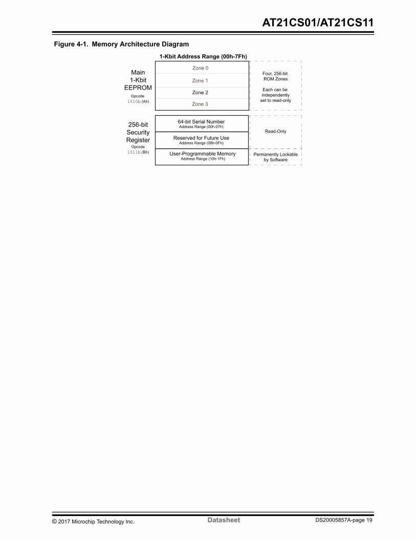
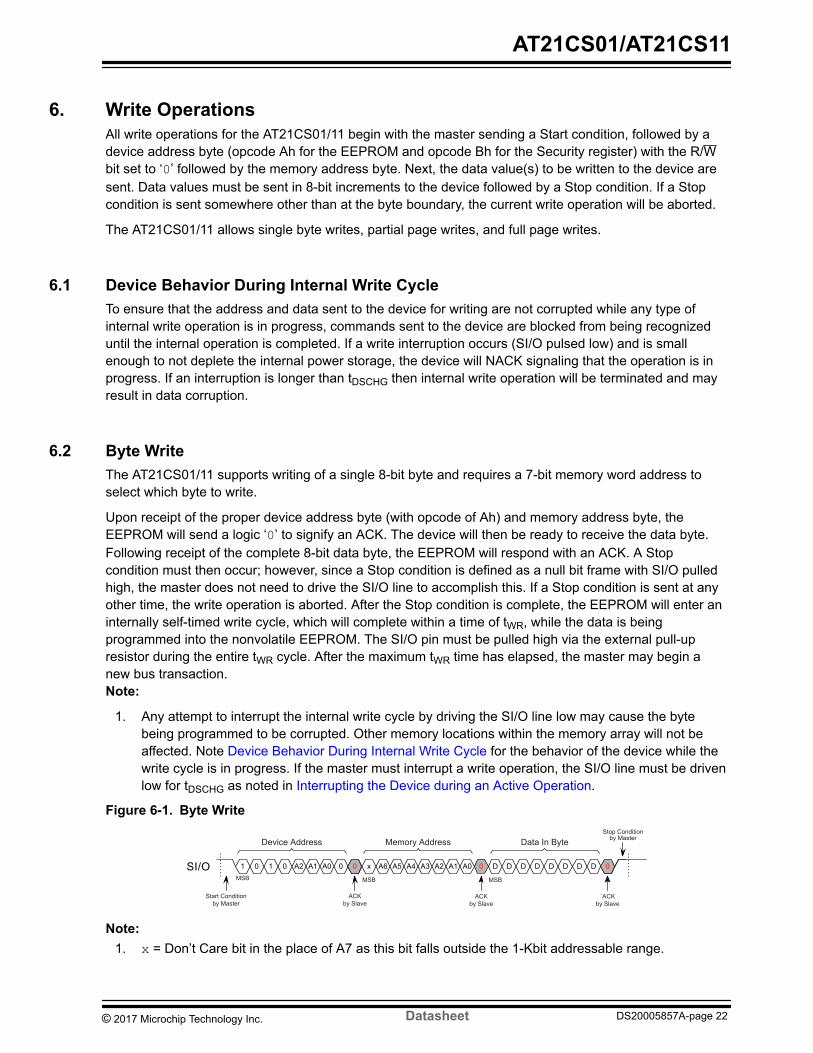
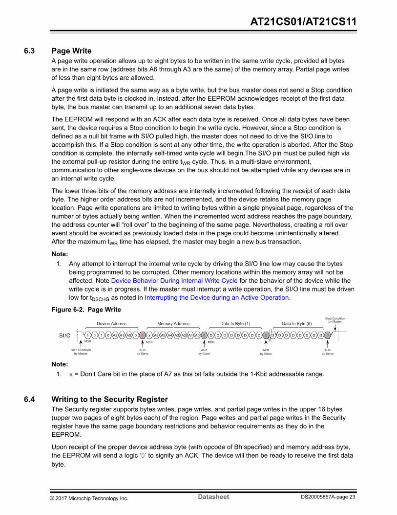
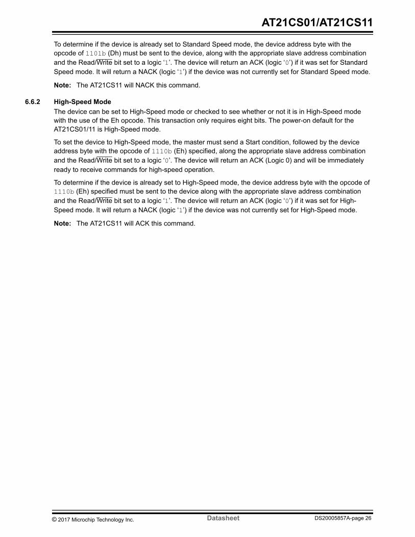
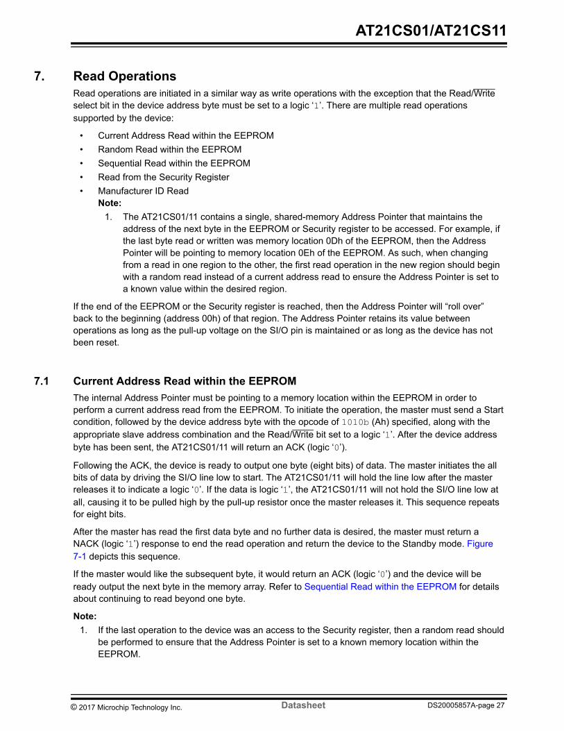
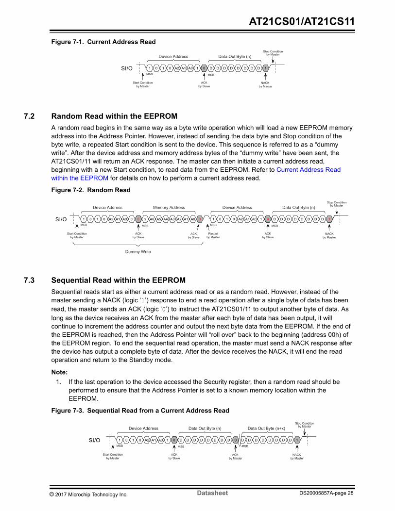
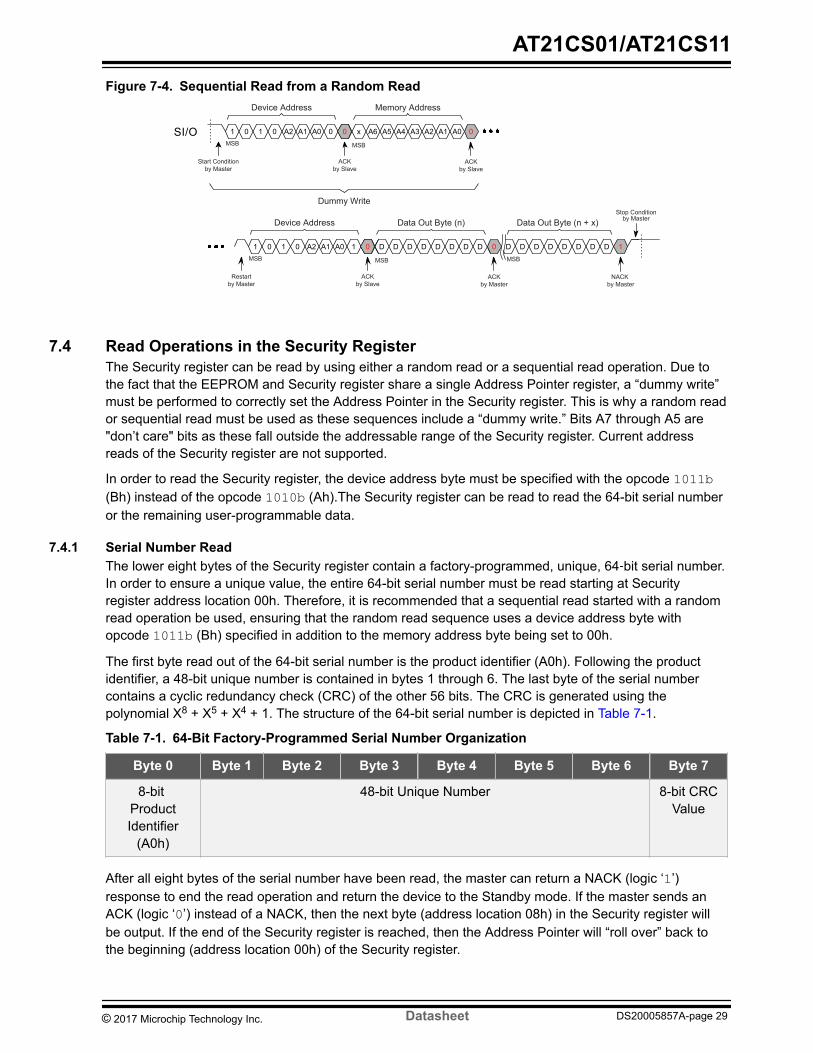
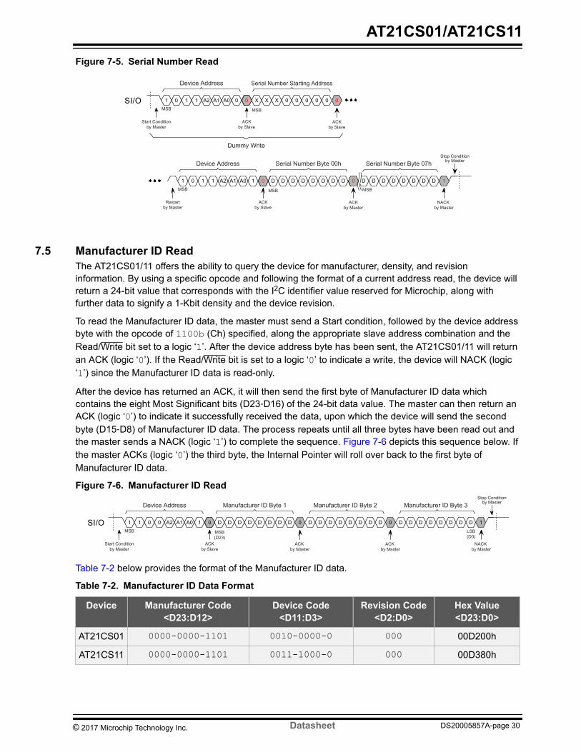
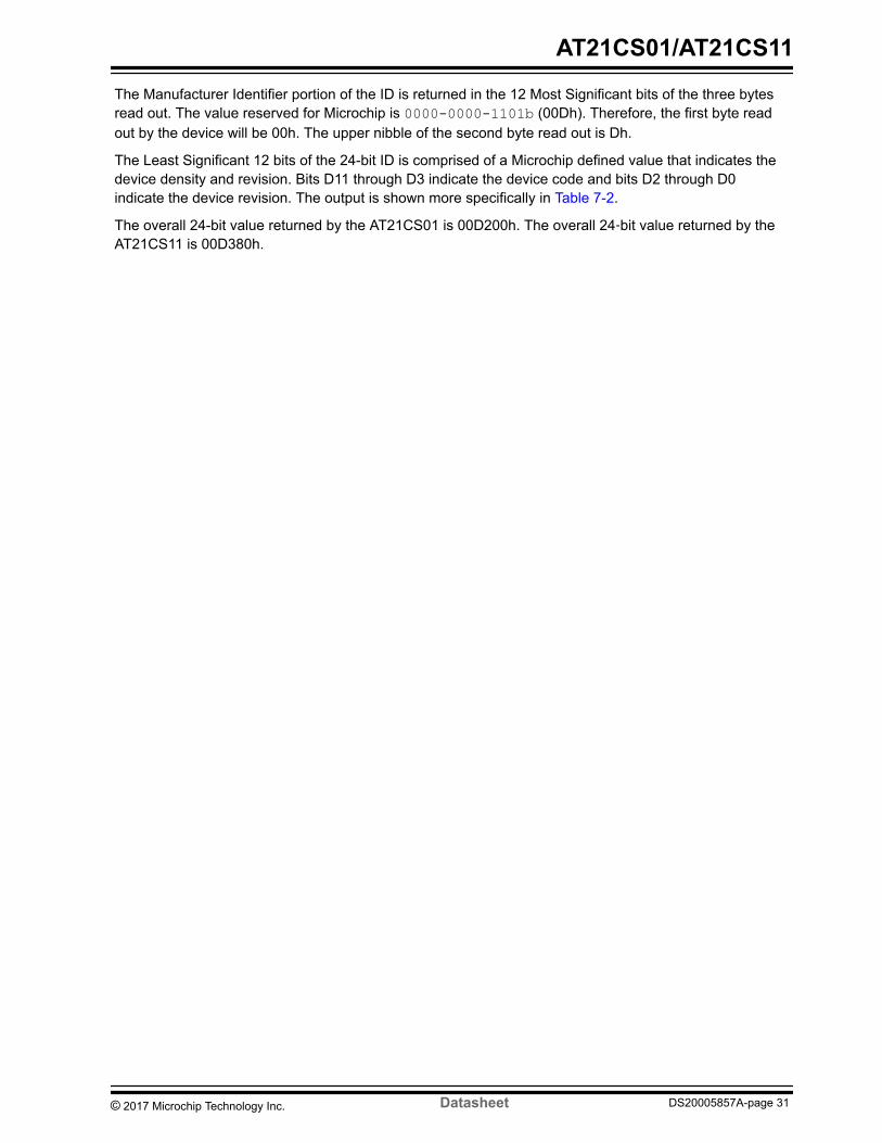
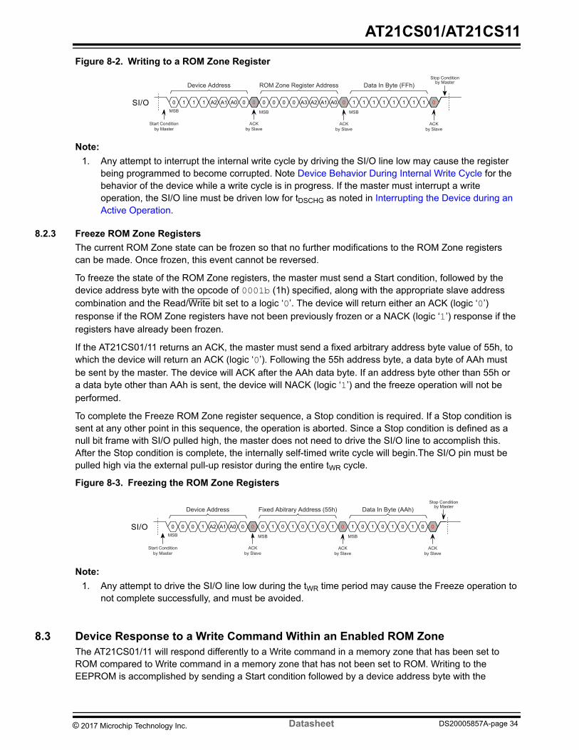

DRAWING NO REV TITLE GPC
2MS-1 B
101414
2MS-1 2-pad 50x35 mm Body 040 thick Extra Thin Single Flat No Lead Package (XSFN) YDR
COMMON DIMENSIONS(Unit of Measure = mm)
SYMBOL MIN TYP MAX NOTE
A 030 035 040
A1 000 0035 005
A3 0127 REF
b 105 110 115 3
L 455 460 465
D 500 BSC
E 350 BSC
e 200 BSC
0 0deg - - 2
K 090 REF
Notes
1 Dimensioning and tolerancing conform to ASME Y145M - 1994
2 All dimensions are in millimeters 0 is in degrees
3 Dimension lsquobrsquo applies to metallized terminal and is measured between 015 and 030mm from terminal tip If the terminal has the optional radius on the
other end of the terminal the dimension lsquobrsquo should not be measured in that radius area
4 Maximum package warpage is 005mm
5 Maximum allowable burrs is 0076mm in all directions
6 Pin 1 on top will be laser marked
7 Unilateral coplanarity zone applies to the exposed heat sink slug as well as the terminals
010 m C A Bv 005 C 3
6
TOP VIEW BOTTOM VIEW
(DATUM A)
B
Ak 010 C
4XPin1 Corner
(DATUM B)1
2
A1
SEATING PLANE
A3 C
SIDE VIEW
1
2
D
E
A
7
0
C060 X 45deg
e
bL
0200
0200
K
7
Pin1 Corner
mk 0050 C
h 010 C
Note For the most current package drawings please see the Microchip Packaging Specification locatedat httpwwwmicrochipcompackaging
AT21CS01AT21CS11
copy 2017 Microchip Technology Inc Datasheet DS20005857A-page 38
AT21CS01 [DATASHEET]Atmel-8903A-SEEPROM-AT21CS01-Datasheet_082015
34
122 3ST1 mdash 3-lead SOT23
TITLE DRAWING NOGPC REV 3TS1
121109
COMMON DIMENSIONS(Unit of Measure = mm)
SYMBOL MIN NOM MAX NOTE
End View
Side View
Top View
3TS1 3-lead 130mm Body Plastic ThinShrink Small Outline Package (Shrink SOT)
BTBG
089001088280210120
030
AA1A2DEE1L1e1b
---
290-
130054 REF190 BSC
-
112010102304264140
050
12
12
3
Notes 1 Dimension D does not include mold flash protrusions or gate burrs Mold flash protrusions or gate burrs shall not exceed 025mm per end Dimension E1 does not include interlead flash or protrusion Interlead flash or protrusion shall not exceed 025mm per side
2 The package top may be smaller than the package bottomDimensions D and E1 are determined at the outermost extremes of the plastic body exclusive of mold flash tie bar burrs gate burrs and interlead flash but including any mismatch between the top and bottom of the plastic body
3 These dimensions apply to the flat section of the lead between008 mm and 015mm from the lead tip
This drawing is for general information only Refer to JEDEC Drawing TO-236 Variation AB for additional information
C L
L1
3
EE1
1 2e1
SEATINGPLANE
b
A2 A
A1e
D
GND
SDA VCC
Note For the most current package drawings please see the Microchip Packaging Specification locatedat httpwwwmicrochipcompackaging
AT21CS01AT21CS11
copy 2017 Microchip Technology Inc Datasheet DS20005857A-page 39
33AT21CS01 [DATASHEET]Atmel-8903A-SEEPROM-AT21CS01-Datasheet_082015
12 Packaging Information
121 8S1 mdash 8-lead SOIC
DRAWING NO REV TITLE GPC
COMMON DIMENSIONS(Unit of Measure = mm)
SYMBOL MIN NOM MAX NOTE
A1 010 ndash 025 A ndash ndash 175
b 031 ndash 051 C 017 ndash 025 D 490 BSC E 600 BSC E1 390 BSC
e 127 BSC L 040 ndash 127 OslashOslash 0deg ndash 8deg
Oslash
E
1
N
TOP VIEW
C
E1
END VIEW
Ab
L
A1
e
D
SIDE VIEW
8S1 H
362015
Notes This drawing is for general information onlyRefer to JEDEC Drawing MS-012 Variation AAfor proper dimensions tolerances datums etc
8S1 8-lead (0150rdquo Wide Body) Plastic Gull Wing Small Outline (JEDEC SOIC) SWB
Note For the most current package drawings please see the Microchip Packaging Specification locatedat httpwwwmicrochipcompackaging
AT21CS01AT21CS11
copy 2017 Microchip Technology Inc Datasheet DS20005857A-page 40
35AT21CS01 [DATASHEET]Atmel-8903A-SEEPROM-AT21CS01-Datasheet_082015
123 4U-6 mdash 4-ball WLCSP
DRAWING NO REV TITLE GPC
4U-6 B
8715
4U-6 4-ball 2x2 Array 040mm PitchWafer Level Chip-Scale Package (WLCSP) with BSC GPH
COMMON DIMENSIONS(Unit of Measure = mm)
SYMBOL MIN TYP MAX NOTEA 0313 0334 0355
A1 mdash 0094 mdash
A2 mdash 0240 mdash 3
D Contact Microchip for details
d1 0400 BSC
E Contact Microchip for details
e1 0400 BSC
b 0170 0185 0200
PIN ASSIGNMENT MATRIX
1 2
A
B
SIO
GND
NC
NC
TOP VIEW
SIDE VIEW
BOTTOM SIDE
Note 1 Dimensions are NOT to scale2 Solder ball composition is 955Sn-40Ag-05Cu3 Product offered with Back Side Coating
k 0015 (4X)
A
B
Ck 0075 C
SEATING PLANE
d b
A1 CORNERA1 CORNER
d 0015 m Cv 005 C A Bmd
D
E
d1
e1
A2A1
A
A
B
12
B
A
1 2
Note For the most current package drawings please see the Microchip Packaging Specification locatedat httpwwwmicrochipcompackaging
AT21CS01AT21CS11
copy 2017 Microchip Technology Inc Datasheet DS20005857A-page 41
11 Revision History
Atmel AT21CS01 Document 8903 Revision A (August 2015)Initial document release
Atmel AT21CS11 Document 8975 Revision A (August 2015)Initial document release Preliminary Status
Atmel AT21CS11 Document 8975 Revision B (November 2015)Removed Standard Speed mode
Revision A (October 2017)Updated to Microchip template This replaces Atmel documents 8903 and 8975 Added XSFN packageUpdated DC output current absolute maximum rating Removed lead finish designation Updated tracecode format in package markings
AT21CS01AT21CS11
copy 2017 Microchip Technology Inc Datasheet DS20005857A-page 42
The Microchip Web Site
Microchip provides online support via our web site at httpwwwmicrochipcom This web site is used asa means to make files and information easily available to customers Accessible by using your favoriteInternet browser the web site contains the following information
bull Product Support ndash Data sheets and errata application notes and sample programs designresources userrsquos guides and hardware support documents latest software releases and archivedsoftware
bull General Technical Support ndash Frequently Asked Questions (FAQ) technical support requestsonline discussion groups Microchip consultant program member listing
bull Business of Microchip ndash Product selector and ordering guides latest Microchip press releaseslisting of seminars and events listings of Microchip sales offices distributors and factoryrepresentatives
Customer Change Notification Service
Microchiprsquos customer notification service helps keep customers current on Microchip productsSubscribers will receive e-mail notification whenever there are changes updates revisions or erratarelated to a specified product family or development tool of interest
To register access the Microchip web site at httpwwwmicrochipcom Under ldquoSupportrdquo click onldquoCustomer Change Notificationrdquo and follow the registration instructions
Customer Support
Users of Microchip products can receive assistance through several channels
bull Distributor or Representativebull Local Sales Officebull Field Application Engineer (FAE)bull Technical Support
Customers should contact their distributor representative or Field Application Engineer (FAE) for supportLocal sales offices are also available to help customers A listing of sales offices and locations is includedin the back of this document
Technical support is available through the web site at httpwwwmicrochipcomsupport
AT21CS01AT21CS11
copy 2017 Microchip Technology Inc Datasheet DS20005857A-page 43
Product Identification System
To order or obtain information eg on pricing or delivery refer to the factory or the listed sales office
Tape and Reel Option
PART NO XX X XDevice Package Device
GradeOperating Voltage
ProductVariation
XX X[1]
Device AT21CS0111 Single-Wire IO Powered 1‑Kbit (128 x 8) Serial EEPROMwith Unique Factory‑Programmed 64‑bit Serial Number
Package Option MS = 2-Pad XSFN
ST = 3-Lead SOT23
SS = 8-Lead SOIC
U = 4-Ball WLCSP (AT21CS01 only)
WWU = Wafer Unsawn
Package Device Grade orWaferDie Thickness
H = Green Industrial Temperature Range (-40degC to +85degC)
U = Green Industrial Temperature Range (‑40degC to +85degC)
11 = 11 mil Wafer Thickness
Operating Voltage M = 17V to 36V (AT21CS01)
blank = 27V to 45V (AT21CS11)
Product Variation 10 = 0-0-0 Slave Address (A2 A1 A0)(2)
0B = 0-0-0 Slave Address (A2 A1 A0) WLCSP package with BackSide Coating
Tape and Reel Option B = Standard packaging (tube or tray)
T = Tape and Reel(1)
Note 1 Tape and Reel identifier only appears in the catalog part number description This identifier is used
for ordering purposes and is not printed on the device package Check with your Microchip SalesOffice for package availability with the Tape and Reel option
2 Please contact Microchip Sales to order devices with non 0-0-0 slave addresses
Examplesbull AT21CS01-SSHM10-T 17V-36V Industrial Temp Tape and Reel SOIC package
Slave Address 0-0-0bull AT21CS01-SSHM11-B 17V-36V Industrial Temp SOIC package Slave Address 0-0-1(2)
bull AT21CS01-MSHM15-T 17V-36V Industrial Temp Tape and Reel XSFN packageSlave Address 1-0-1(2)
bull AT21CS01-UUM0B-T 17V-36V Industrial Temp Tape and Reel UDFN packageSlave Address 0-0-0
AT21CS01AT21CS11
copy 2017 Microchip Technology Inc Datasheet DS20005857A-page 44
bull AT21CS11-STU10 27V-45V Industrial Temp SOT23 package Slave Address 0-0-0bull AT21CS11-MSH17-T 27V-45V Industrial Temp XSFN package Slave Address 1-1-1(2)
bull AT21CS11-WWU11(1) 27V-45V Industrial Temp 11 mil Thick Wafer ThicknessSlave Address 0-0-0 all die
Note 1 Contact Microchip Sales for wafer sales2 Please contact Microchip Sales to order non 0-0-0 slave addressed devices
Microchip Devices Code Protection Feature
Note the following details of the code protection feature on Microchip devices
bull Microchip products meet the specification contained in their particular Microchip Data Sheetbull Microchip believes that its family of products is one of the most secure families of its kind on the
market today when used in the intended manner and under normal conditionsbull There are dishonest and possibly illegal methods used to breach the code protection feature All of
these methods to our knowledge require using the Microchip products in a manner outside theoperating specifications contained in Microchiprsquos Data Sheets Most likely the person doing so isengaged in theft of intellectual property
bull Microchip is willing to work with the customer who is concerned about the integrity of their codebull Neither Microchip nor any other semiconductor manufacturer can guarantee the security of their
code Code protection does not mean that we are guaranteeing the product as ldquounbreakablerdquo
Code protection is constantly evolving We at Microchip are committed to continuously improving thecode protection features of our products Attempts to break Microchiprsquos code protection feature may be aviolation of the Digital Millennium Copyright Act If such acts allow unauthorized access to your softwareor other copyrighted work you may have a right to sue for relief under that Act
Legal Notice
Information contained in this publication regarding device applications and the like is provided only foryour convenience and may be superseded by updates It is your responsibility to ensure that yourapplication meets with your specifications MICROCHIP MAKES NO REPRESENTATIONS ORWARRANTIES OF ANY KIND WHETHER EXPRESS OR IMPLIED WRITTEN OR ORAL STATUTORYOR OTHERWISE RELATED TO THE INFORMATION INCLUDING BUT NOT LIMITED TO ITSCONDITION QUALITY PERFORMANCE MERCHANTABILITY OR FITNESS FOR PURPOSEMicrochip disclaims all liability arising from this information and its use Use of Microchip devices in lifesupport andor safety applications is entirely at the buyerrsquos risk and the buyer agrees to defendindemnify and hold harmless Microchip from any and all damages claims suits or expenses resultingfrom such use No licenses are conveyed implicitly or otherwise under any Microchip intellectualproperty rights unless otherwise stated
Trademarks
The Microchip name and logo the Microchip logo AnyRate AVR AVR logo AVR Freaks BeaconThingsBitCloud CryptoMemory CryptoRF dsPIC FlashFlex flexPWR Heldo JukeBlox KeeLoq KeeLoq logoKleer LANCheck LINK MD maXStylus maXTouch MediaLB megaAVR MOST MOST logo MPLABOptoLyzer PIC picoPower PICSTART PIC32 logo Prochip Designer QTouch RightTouch SAM-BA
AT21CS01AT21CS11
copy 2017 Microchip Technology Inc Datasheet DS20005857A-page 45
SpyNIC SST SST Logo SuperFlash tinyAVR UNIO and XMEGA are registered trademarks ofMicrochip Technology Incorporated in the USA and other countries
ClockWorks The Embedded Control Solutions Company EtherSynch Hyper Speed Control HyperLightLoad IntelliMOS mTouch Precision Edge and Quiet-Wire are registered trademarks of MicrochipTechnology Incorporated in the USA
Adjacent Key Suppression AKS Analog-for-the-Digital Age Any Capacitor AnyIn AnyOut BodyComchipKIT chipKIT logo CodeGuard CryptoAuthentication CryptoCompanion CryptoControllerdsPICDEM dsPICDEMnet Dynamic Average Matching DAM ECAN EtherGREEN In-Circuit SerialProgramming ICSP Inter-Chip Connectivity JitterBlocker KleerNet KleerNet logo Mindi MiWimotorBench MPASM MPF MPLAB Certified logo MPLIB MPLINK MultiTRAK NetDetach OmniscientCode Generation PICDEM PICDEMnet PICkit PICtail PureSilicon QMatrix RightTouch logo REALICE Ripple Blocker SAM-ICE Serial Quad IO SMART-IS SQI SuperSwitcher SuperSwitcher II TotalEndurance TSHARC USBCheck VariSense ViewSpan WiperLock Wireless DNA and ZENA aretrademarks of Microchip Technology Incorporated in the USA and other countries
SQTP is a service mark of Microchip Technology Incorporated in the USA
Silicon Storage Technology is a registered trademark of Microchip Technology Inc in other countries
GestIC is a registered trademark of Microchip Technology Germany II GmbH amp Co KG a subsidiary ofMicrochip Technology Inc in other countries
All other trademarks mentioned herein are property of their respective companiescopy 2017 Microchip Technology Incorporated Printed in the USA All Rights Reserved
ISBN 978-1-5224-2232-7
Quality Management System Certified by DNV
ISOTS 16949Microchip received ISOTS-169492009 certification for its worldwide headquarters design and waferfabrication facilities in Chandler and Tempe Arizona Gresham Oregon and design centers in Californiaand India The Companyrsquos quality system processes and procedures are for its PICreg MCUs and dsPICreg
DSCs KEELOQreg code hopping devices Serial EEPROMs microperipherals nonvolatile memory andanalog products In addition Microchiprsquos quality system for the design and manufacture of developmentsystems is ISO 90012000 certified
AT21CS01AT21CS11
copy 2017 Microchip Technology Inc Datasheet DS20005857A-page 46
AMERICAS ASIAPACIFIC ASIAPACIFIC EUROPECorporate Office2355 West Chandler BlvdChandler AZ 85224-6199Tel 480-792-7200Fax 480-792-7277Technical SupporthttpwwwmicrochipcomsupportWeb AddresswwwmicrochipcomAtlantaDuluth GATel 678-957-9614Fax 678-957-1455Austin TXTel 512-257-3370BostonWestborough MATel 774-760-0087Fax 774-760-0088ChicagoItasca ILTel 630-285-0071Fax 630-285-0075DallasAddison TXTel 972-818-7423Fax 972-818-2924DetroitNovi MITel 248-848-4000Houston TXTel 281-894-5983IndianapolisNoblesville INTel 317-773-8323Fax 317-773-5453Tel 317-536-2380Los AngelesMission Viejo CATel 949-462-9523Fax 949-462-9608Tel 951-273-7800Raleigh NCTel 919-844-7510New York NYTel 631-435-6000San Jose CATel 408-735-9110Tel 408-436-4270Canada - TorontoTel 905-695-1980Fax 905-695-2078
Asia Pacific OfficeSuites 3707-14 37th FloorTower 6 The GatewayHarbour City KowloonHong KongTel 852-2943-5100Fax 852-2401-3431Australia - SydneyTel 61-2-9868-6733Fax 61-2-9868-6755China - BeijingTel 86-10-8569-7000Fax 86-10-8528-2104China - ChengduTel 86-28-8665-5511Fax 86-28-8665-7889China - ChongqingTel 86-23-8980-9588Fax 86-23-8980-9500China - DongguanTel 86-769-8702-9880China - GuangzhouTel 86-20-8755-8029China - HangzhouTel 86-571-8792-8115Fax 86-571-8792-8116China - Hong Kong SARTel 852-2943-5100Fax 852-2401-3431China - NanjingTel 86-25-8473-2460Fax 86-25-8473-2470China - QingdaoTel 86-532-8502-7355Fax 86-532-8502-7205China - ShanghaiTel 86-21-3326-8000Fax 86-21-3326-8021China - ShenyangTel 86-24-2334-2829Fax 86-24-2334-2393China - ShenzhenTel 86-755-8864-2200Fax 86-755-8203-1760China - WuhanTel 86-27-5980-5300Fax 86-27-5980-5118China - XianTel 86-29-8833-7252Fax 86-29-8833-7256
China - XiamenTel 86-592-2388138Fax 86-592-2388130China - ZhuhaiTel 86-756-3210040Fax 86-756-3210049India - BangaloreTel 91-80-3090-4444Fax 91-80-3090-4123India - New DelhiTel 91-11-4160-8631Fax 91-11-4160-8632India - PuneTel 91-20-3019-1500Japan - OsakaTel 81-6-6152-7160Fax 81-6-6152-9310Japan - TokyoTel 81-3-6880- 3770Fax 81-3-6880-3771Korea - DaeguTel 82-53-744-4301Fax 82-53-744-4302Korea - SeoulTel 82-2-554-7200Fax 82-2-558-5932 or82-2-558-5934Malaysia - Kuala LumpurTel 60-3-6201-9857Fax 60-3-6201-9859Malaysia - PenangTel 60-4-227-8870Fax 60-4-227-4068Philippines - ManilaTel 63-2-634-9065Fax 63-2-634-9069SingaporeTel 65-6334-8870Fax 65-6334-8850Taiwan - Hsin ChuTel 886-3-5778-366Fax 886-3-5770-955Taiwan - KaohsiungTel 886-7-213-7830Taiwan - TaipeiTel 886-2-2508-8600Fax 886-2-2508-0102Thailand - BangkokTel 66-2-694-1351Fax 66-2-694-1350
Austria - WelsTel 43-7242-2244-39Fax 43-7242-2244-393Denmark - CopenhagenTel 45-4450-2828Fax 45-4485-2829Finland - EspooTel 358-9-4520-820France - ParisTel 33-1-69-53-63-20Fax 33-1-69-30-90-79France - Saint CloudTel 33-1-30-60-70-00Germany - GarchingTel 49-8931-9700Germany - HaanTel 49-2129-3766400Germany - HeilbronnTel 49-7131-67-3636Germany - KarlsruheTel 49-721-625370Germany - MunichTel 49-89-627-144-0Fax 49-89-627-144-44Germany - RosenheimTel 49-8031-354-560Israel - RarsquoananaTel 972-9-744-7705Italy - MilanTel 39-0331-742611Fax 39-0331-466781Italy - PadovaTel 39-049-7625286Netherlands - DrunenTel 31-416-690399Fax 31-416-690340Norway - TrondheimTel 47-7289-7561Poland - WarsawTel 48-22-3325737Romania - BucharestTel 40-21-407-87-50Spain - MadridTel 34-91-708-08-90Fax 34-91-708-08-91Sweden - GothenbergTel 46-31-704-60-40Sweden - StockholmTel 46-8-5090-4654UK - WokinghamTel 44-118-921-5800Fax 44-118-921-5820
Worldwide Sales and Service
copy 2017 Microchip Technology Inc Datasheet DS20005857A-page 47
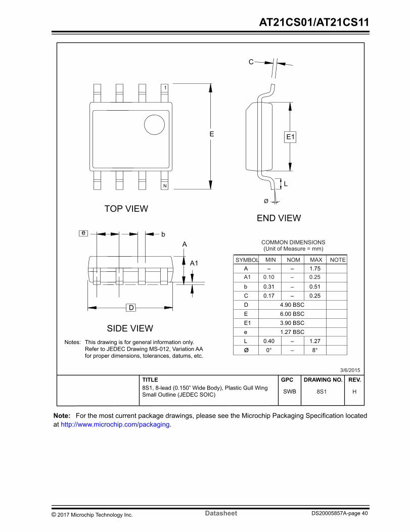
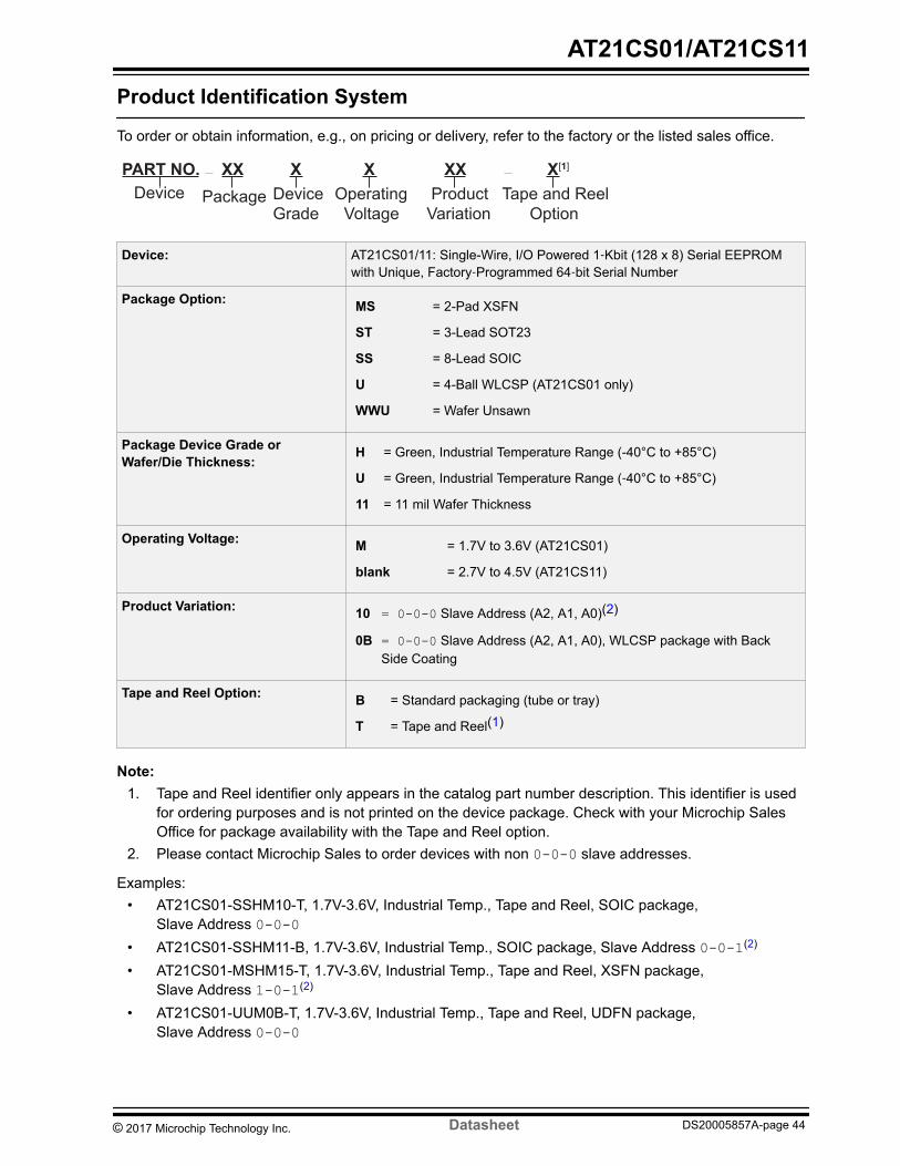