Embed Size (px)
Citation preview
i
ASYNCHRONOUS DESIGN OF SYSTOLIC ARRAY ARCHITECTURES IN CMOS
A THESIS SUBMITTED TO THE GRADUATE SCHOOL OF NATURAL AND APPLIED SCIENCES
OF MIDDLE EAST TECHNICAL UNIVERSITY
BY
A. NESLİN İSMAİLOĞLU
IN PARTIAL FULFILLMENT OF THE REQUIREMENTS FOR THE DEGREE OF
DOCTOR OF PHILOSOPHY IN
ELECTRICAL AND ELECTRONICS ENGINEERING
APRIL 2008

ii
ii
Approval of the Thesis
“ASYNCHRONOUS DESIGN OF SYSTOLIC ARRAY ARCHITECTURES IN CMOS”
Submitted by A. NESLİN İSMAİLOĞLU in partial fulfillment of the requirements for the degree of Doctor of Philosophy in Electrical and Electronics Engineering by, Prof. Dr. Canan ÖZGEN Dean, Graduate School of Natural And Applied Sciences Prof. Dr. İsmet ERKMEN Head of Department, Electrical and Electronics Engineering Prof. Dr. Murat AŞKAR Supervisor, Electrical and Electronics Engineering Examining Committee Members: Prof. Dr. Hasan GÜRAN (*) Electrical and Electronics Engineering, METU Prof. Dr. Murat AŞKAR (**) Electrical and Electronics Engineering, METU Prof. Dr. Abdullah ATALAR Electrical and Electronics Engineering, Bilkent University Yrd. Doç. Dr. Cüneyt BAZLAMAÇÇI Electrical and Electronics Engineering, METU Yrd. Doç. Dr. Ece SCHMIDT Electrical and Electronics Engineering, METU
Date: (*) Head of Examining Committee (**) Supervisor

iii
I hereby declare that all information in this document has been obtained and presented
in accordance with academic rules and ethical conduct. I also declare that, as required
by these rules and conduct, I have fully cited and referenced all material and results
that are not original to this work.
Name, Last name: A. NESLİN İSMAİLOĞLU
Signature :
iv
ABSTRACT
ASYNCHRONOUS DESIGN OF SYSTOLIC ARRAY ARCHITECTURES IN CMOS
İSMAİLOĞLU, A. Neslin
Ph.D., Department of Electrical and Electronics Engineering
Supervisor : Prof.. Dr. Murat AŞKAR
April 2008, 96 pages
In this study, delay-insensitive asynchronous circuit design style has been adopted to systolic
array architectures to exploit the benefits of both techniques for improved throughput. A
delay-insensitivity verification analysis method employing symbolic delays is proposed for
bit-level pipelined asynchronous circuits. The proposed verification method allows data-
dependent early output evaluation to co-exist with robust delay-insensitive circuit behavior
in pipelined architectures such as systolic arrays. Regardless of the length of the pipeline,
delay-insensitivity verification of a systolic array with early output evaluation paths in one-
dimension is reduced to analysis of three adjacent systoles for eight possible early/late
output evaluation scenarios. Analyzing both combinational and sequential parts
concurrently, delay-insensitivity violations are located and corrected at structural level,
without diminishing the early output evaluation benefits. Since symbolic delays are used
without imposing any timing constraints on the environment; the method is technology
independent and robust against all physical and environmental variations. To demonstrate
the verification method, adders are selected for being at the core of data processing systems.
Two asynchronous adder topologies in the delay-insensitive dual-rail threshold logic style,
having data-dependent early carry evaluation paths, are converted into bit-level pipelined
systolic arrays. On these adders, data-dependent delay-insensitivity violations are detected
and resolved using the proposed verification technique. The modified adders achieved the
targeted O(log2n) average completion time and -as a result of bit-level pipelining- nearly
constant throughput against increased bit-length. The delay-insensitivity verification method
could further be extended to handle more early output evaluation paths in multi-dimension.
Keywords: Asynchronous Logic Circuits, Pipeline Arithmetic, Pipeline Processing, Systolic
Arrays.
v
ÖZ
CMOS DEVRELERLE ASENKRON SİSTOLİK DİZİ MİMARİSİ TASARIMI
İSMAİLOĞLU, A. Neslin
Doktora, Elektrik ve Elektronik Mühendisliği Bölümü
Tez Yöneticisi : Prof.. Dr. Murat AŞKAR
Nisan 2008, 96 sayfa
Bu çalışmada, asenkron devre tasarım yöntemi sistolik dizilere uyarlanarak her iki yöntemin
faydalarının birleştirilmesi ve veri işlem hacminin arttırılması amaçlanmıştır. Bit-
seviyesinde boru hattı mimarisine sahip asenkron sistolik diziler için, sembolik gecikme
değerleri kullanımına dayalı bir gecikmeye-duyarsızlık analiz ve doğrulama yöntemi
önerilmiştir. Önerilen doğrulama yöntemi, bit-seviyesinde boru hatlandırılmış asenkron
sistolik dizilerde, erken ve girdi-tamlığı olmayan çıktı üretimi durumunda gecikmeye-
duyarsızlık isterlerinin güvenli bir şekilde karşılanmasını sağlar. Sistolik dizinin
uzunluğundan bağımsız olarak, tek yönde erken çıktı üretimi olan bir sistolik dizinin
gecikmeye-duyarsızlık analizi, üç adet komşu sistolün olası sekiz adet erken/geç çıktı üretme
senaryoları için analizine indirgenmiştir. Hem işlem hem de kayıt yapan birimler birarada
analiz edilerek, gecikmeye-duyarsızlık ihlalleri yapısal seviyede belirlenmekte ve erken çıktı
üretiminin sağladığı hızlanmadan ödün vermeden düzeltilmektedir. Bu yöntem, sembolik
gecikme değerleri kullanarak ve çevre birimlere herhangi bir zaman kısıtı getirmeden
doğrulama yaptığı için, fiziksel ve çevresel etkilere karşı gürbüzdür, dolayısıyla devre üretim
teknolojisinden de bağımsızdır. Önerilen yönteminin gösterimi için, veri işleme yapılarının
temelini oluşturan toplayıcılar seçilmiştir. Çift-hatlı eşikli mantık tipinde ve erken elde
üretebilen iki adet asenkron toplayıcı bit-seviyesinde boru hatlandırılmış asenkron sistolik
dizilere dönüştürülmüştür. Bu toplayıcılardaki girdiye bağlı gecikmeye-duyarsızlık ihlalleri
önerilen doğrulama yöntemiyle saptanmış ve düzeltilmiştir. Düzeltilmiş toplayıcılar, -bit-
seviyesinde boru hatlandırma sayesinde- O(log2n) ortalama işlem süresi ve bit uzunluğundan
bağımsız sabite yakın veri hacmi hedefine ulaşmaktadır. Gecikmeye-duyarsızlık doğrulama
yöntemi daha çok sayıda ve yönde erken çıktı üreten sistolik dizileri de kapsayacak şekilde
geliştirilmeye açıktır.

vi
Anahtar Kelimeler: Asenkron mantık devreleri, Boru-hattı aritmetiği, Boru-hattı işlemleri,
Sistolik diziler.

vii
“All that is gold does not glitterNot all those who wander are lost”
J.R.R. Tolkien
To all wanderers

viii
ACKNOWLEDGMENTS
The author wishes to express her deepest gratitude for her supervisor Prof. Dr. Murat
AŞKAR for his precious guidance, advice, criticism, encouragements and insight throughout
the research.
The author would also like to thank her supervising comittee members Prof. Dr. Hasan
GÜRAN and Prof. Dr. Abdullah ATALAR for their valuable suggestions, comments and
guidance.
The suggestions and comments of comittee members Assist. Prof. Dr. Ece GÜRAN
SCHMIDT and Assist. Prof. Dr. Cüneyt BAZLAMAÇCI are gratefully acknowledged.
The author also wishes to express her gratitude for her former supervisor Dr. Çağatay
TEKMEN for his support, assitance and encouragement at the begining of the research.
The author also wishes to thank TÜBİTAK-UZAY (formerly TÜBİTAK-ODTÜ- BİLTEN)
for the facilities and environment provided to her throughout the research and for the support
given to her for publications. The author’s colleagues and friends at TÜBİTAK-UZAY are
also appreciated for all the support and encouragement she received from them.
The author thanks especially to her family for their amazing love, constant support, great
patience and extensive encouragement throughout her studies.
ix
TABLE OF CONTENTS
ABSTRACT ........................................................................................................................... iv
ÖZ ......................................................................................................................................... v
ACKNOWLEDGMENTS ....................................................................................................viii
TABLE OF CONTENTS........................................................................................................ ix
LIST OF ABBREVIATIONS................................................................................................xii
LIST OF FIGURES ..............................................................................................................xiii
LIST OF TABLES................................................................................................................xiv
CHAPTERS
1 INTRODUCTION ........................................................................................................... 1
1.1 Benefits of Asynchronous Design ........................................................................... 3 1.2 Difficulties of Asynchronous Design....................................................................... 5 1.3 When to Use Asynchronous Design? ...................................................................... 6 1.4 Main Features of Asynchronous Circuits................................................................. 6
1.4.1 Delay models ................................................................................................... 7 1.4.2 Signaling and Handshaking Conventions ........................................................ 8 1.4.3 Data Representation ......................................................................................... 9 1.4.4 Elastic Micropipelines ................................................................................... 11
1.5 Systolic Arrays in Asynchronous........................................................................... 11 1.6 Thesis Outline ........................................................................................................ 13
2 DELAY INSENSITIVE ASYNCHRONOUS DESIGN ............................................... 14
2.1 Delay Insensitive Design Styles............................................................................. 14 2.2 Dual-Rail Threshold Logic Gates .......................................................................... 15
2.2.1 Symbolic Completeness of Expression.......................................................... 15 2.2.2 Two-Phase Operation..................................................................................... 16 2.2.3 Logic Design using Dual Rail Threshold Logic Gates .................................. 17 2.2.4 Transistor Level Design of Dual Rail Threshold Logic Gates....................... 18 2.2.5 Registration and Pipelining............................................................................ 19
2.3 Delay Insensitivity Criteria .................................................................................... 20 2.4 Pipelining Criteria.................................................................................................. 21
3 VERIFICATION OF DELAY INSENSITIVITY ......................................................... 23
x
3.1 Formal Verification Methods and State Explosion Problem ................................. 23 3.2 Recent Alternative Methodologies ........................................................................ 24
3.2.1 Relative Timing Assumptions........................................................................ 25 3.2.2 Lazy Transition Systems................................................................................ 25 3.2.3 Symbolic Methods ......................................................................................... 25 3.2.4 Partial Completion Methods with Early Evaluation ...................................... 25
3.3 Early Outputs Conflict ........................................................................................... 26 3.3.1 Early Output Evaluation vs. Delay Insensitivity............................................ 26 3.3.2 Demonstration on a Systolic Array................................................................ 27
4 DELAY-INSENSITIVITY VERIFICATION METHOD FOR SYSTOLIC ARRAYS31
4.1 Structural Delay Insensitivity Verification Analysis Method (SDIVA) ................ 32 4.1.1 Symbolic Delay Assignment.......................................................................... 32 4.1.2 Initial Assumptions ........................................................................................ 33 4.1.3 Analysis with Symbolic Delays ..................................................................... 34
4.2 Structural Modifications Inferred .......................................................................... 44 4.3 Benefits of the SDIVA Method ............................................................................. 49
5 DELAY INSENSITIVE SYSTOLIC ADDER DESIGN .............................................. 50
5.1 Delay Insensitive Adders with Early Carry Evaluation ......................................... 52 5.2 Application of Pipelining and Early Carry Evaluation Conflict ............................ 55
5.2.1 DI CSA Systole.............................................................................................. 55 5.2.2 NCL Adder Systole........................................................................................ 61
5.3 Fixing Early Carry Evaluation Conflict with Structural Modifications................. 64 5.3.1 Modified DI CSA Systole.............................................................................. 64 5.3.2 Modified NCL Adder Systole........................................................................ 69 5.3.3 Benefits of Modified Systolic DI Adder Structures....................................... 73 5.3.4 Performance Comparison of Systolic DI Adder Structures ........................... 74
5.4 Application of Bit-Skewed Inputs ......................................................................... 77 5.4.1 Bit-skewed Systolic DI CSA Pipeline ........................................................... 78 5.4.2 Bit-skewed Systolic NCL Adder Pipeline ..................................................... 79 5.4.3 Benefits of Bit-skewed Pipelining ................................................................. 79
6 CONCLUSION.............................................................................................................. 80
BIBLIOGRAHPY.................................................................................................................. 84

xi
APPENDIX A: C CODE FOR DICSA ESTIMATION ........................................................ 90
APPENDIX B: C CODE FOR DI NCL ADDER ESTIMATION ....................................... 92
CURRICULUM VITAE........................................................................................................ 94
xii
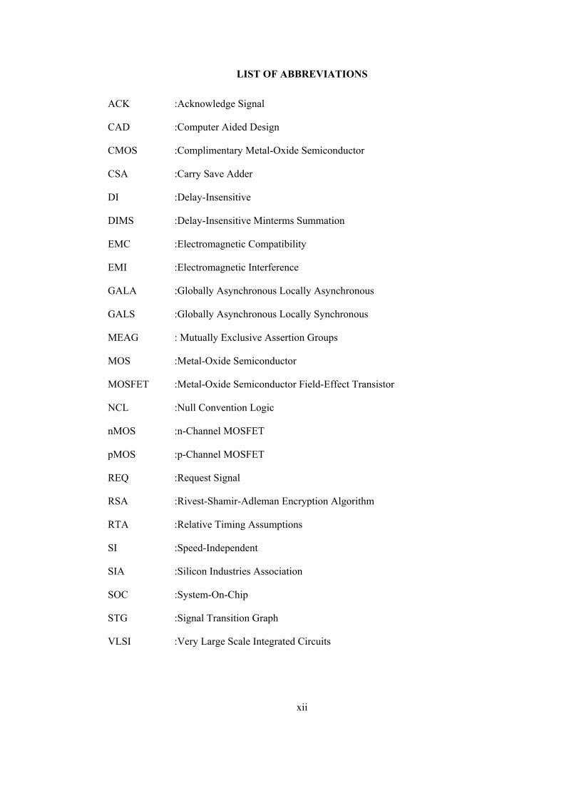
LIST OF ABBREVIATIONS
ACK :Acknowledge Signal
CAD :Computer Aided Design
CMOS :Complimentary Metal-Oxide Semiconductor
CSA :Carry Save Adder
DI :Delay-Insensitive
DIMS :Delay-Insensitive Minterms Summation
EMC :Electromagnetic Compatibility
EMI :Electromagnetic Interference
GALA :Globally Asynchronous Locally Asynchronous
GALS :Globally Asynchronous Locally Synchronous
MEAG : Mutually Exclusive Assertion Groups
MOS :Metal-Oxide Semiconductor
MOSFET :Metal-Oxide Semiconductor Field-Effect Transistor
NCL :Null Convention Logic
nMOS :n-Channel MOSFET
pMOS :p-Channel MOSFET
REQ :Request Signal
RSA :Rivest-Shamir-Adleman Encryption Algorithm
RTA :Relative Timing Assumptions
SI :Speed-Independent
SIA :Silicon Industries Association
SOC :System-On-Chip
STG :Signal Transition Graph
VLSI :Very Large Scale Integrated Circuits
xiii
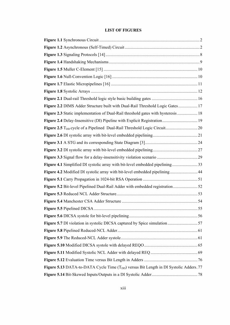
LIST OF FIGURES Figure 1.1 Synchronous Circuit .............................................................................................. 2 Figure 1.2 Asynchronous (Self-Timed) Circuit ...................................................................... 2 Figure 1.3 Signaling Protocols [14] ........................................................................................ 8 Figure 1.4 Handshaking Mechanisms..................................................................................... 9 Figure 1.5 Muller C-Element [15] ........................................................................................ 10 Figure 1.6 Null-Convention Logic [16] ................................................................................ 10 Figure 1.7 Elastic Micropipelines [16] ................................................................................. 11 Figure 1.8 Systolic Arrays .................................................................................................... 12 Figure 2.1 Dual-rail Threshold logic style basic building gates ........................................... 16 Figure 2.2 DIMS Adder Structure built with Dual-Rail Threshold Logic Gates .................. 17 Figure 2.3 Static implementation of Dual-Rail threshold gates with hysteresis ................... 18 Figure 2.4 Delay-Insensitive (DI) Pipeline with Explicit Registration................................. 19 Figure 2.5 TDD cycle of a Pipelined Dual-Rail Threshold Logic Circuit.............................. 20 Figure 2.6 DI systolic array with bit-level embedded pipelining.......................................... 21 Figure 3.1 A STG and its corresponding State Diagram [3]................................................. 24 Figure 3.2 DI systolic array with bit-level embedded pipelining.......................................... 27 Figure 3.3 Signal flow for a delay-insensitivity violation scenario ...................................... 29 Figure 4.1 Simplified DI systolic array with bit-level embedded pipelining........................ 33 Figure 4.2 Modified DI systolic array with bit-level embedded pipelining.......................... 44 Figure 5.1 Carry Propagation in 1024-bit RSA Operation ................................................... 51 Figure 5.2 Bit-level Pipelined Dual-Rail Adder with embedded registration....................... 52 Figure 5.3 Reduced NCL Adder Structure............................................................................ 53 Figure 5.4 Manchester CSA Adder Structure ....................................................................... 54 Figure 5.5 Pipelined DICSA ................................................................................................. 55 Figure 5.6 DICSA systole for bit-level pipelining................................................................ 56 Figure 5.7 DI violation in systolic DICSA captured by Spice simulation ............................ 57 Figure 5.8 Pipelined Reduced-NCL Adder........................................................................... 61 Figure 5.9 The Reduced-NCL Adder systole........................................................................ 61 Figure 5.10 Modified DICSA systole with delayed REQO.................................................. 65 Figure 5.11 Modified Systolic NCL Adder with delayed REQ............................................ 69 Figure 5.12 Evaluation Time versus Bit Length in Adders .................................................. 76 Figure 5.13 DATA-to-DATA Cycle Time (TDD) versus Bit Length in DI Systolic Adders.77 Figure 5.14 Bit-Skewed Inputs/Outputs in a DI Systolic Adder........................................... 78
xiv
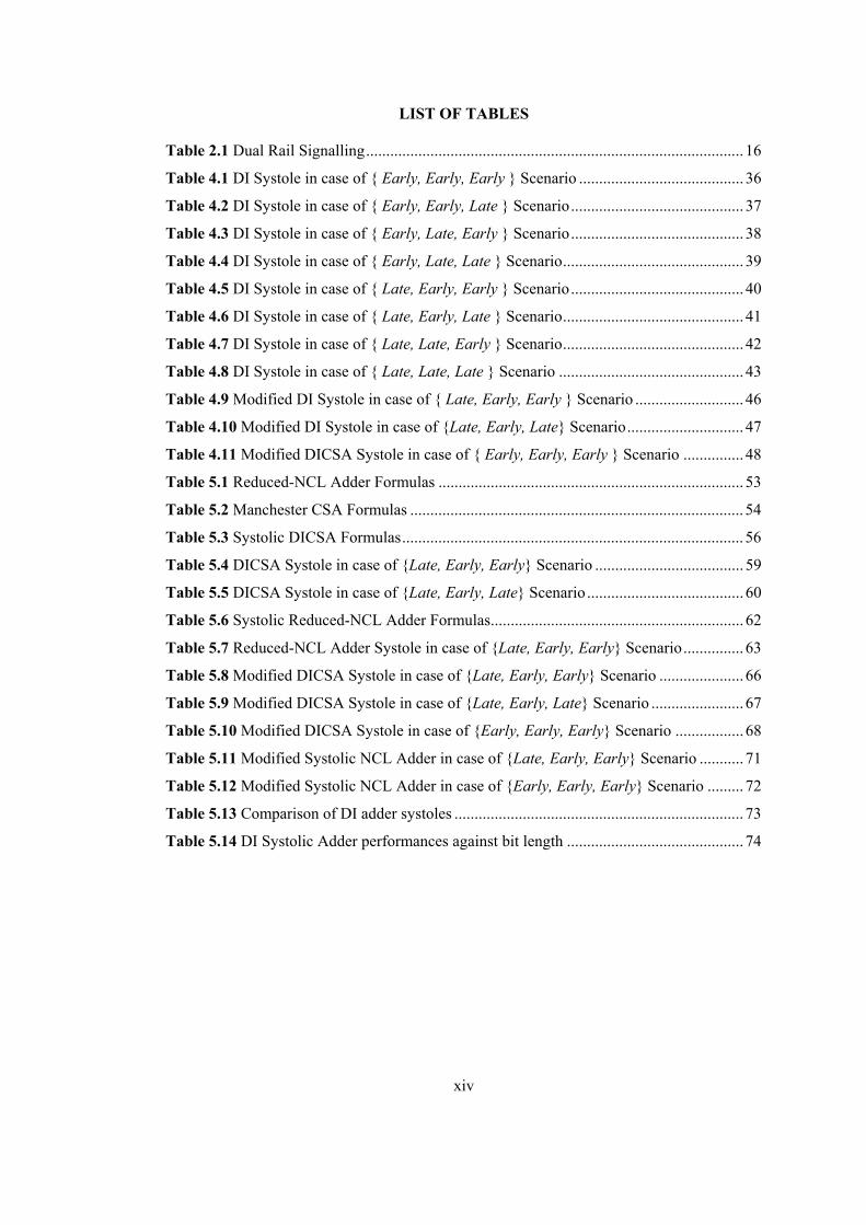
LIST OF TABLES Table 2.1 Dual Rail Signalling.............................................................................................. 16 Table 4.1 DI Systole in case of { Early, Early, Early } Scenario ......................................... 36 Table 4.2 DI Systole in case of { Early, Early, Late } Scenario........................................... 37 Table 4.3 DI Systole in case of { Early, Late, Early } Scenario........................................... 38 Table 4.4 DI Systole in case of { Early, Late, Late } Scenario............................................. 39 Table 4.5 DI Systole in case of { Late, Early, Early } Scenario........................................... 40 Table 4.6 DI Systole in case of { Late, Early, Late } Scenario............................................. 41 Table 4.7 DI Systole in case of { Late, Late, Early } Scenario............................................. 42 Table 4.8 DI Systole in case of { Late, Late, Late } Scenario .............................................. 43 Table 4.9 Modified DI Systole in case of { Late, Early, Early } Scenario ........................... 46 Table 4.10 Modified DI Systole in case of {Late, Early, Late} Scenario............................. 47 Table 4.11 Modified DICSA Systole in case of { Early, Early, Early } Scenario ............... 48 Table 5.1 Reduced-NCL Adder Formulas ............................................................................ 53 Table 5.2 Manchester CSA Formulas ................................................................................... 54 Table 5.3 Systolic DICSA Formulas..................................................................................... 56 Table 5.4 DICSA Systole in case of {Late, Early, Early} Scenario ..................................... 59 Table 5.5 DICSA Systole in case of {Late, Early, Late} Scenario ....................................... 60 Table 5.6 Systolic Reduced-NCL Adder Formulas............................................................... 62 Table 5.7 Reduced-NCL Adder Systole in case of {Late, Early, Early} Scenario............... 63 Table 5.8 Modified DICSA Systole in case of {Late, Early, Early} Scenario ..................... 66 Table 5.9 Modified DICSA Systole in case of {Late, Early, Late} Scenario ....................... 67 Table 5.10 Modified DICSA Systole in case of {Early, Early, Early} Scenario ................. 68 Table 5.11 Modified Systolic NCL Adder in case of {Late, Early, Early} Scenario ........... 71 Table 5.12 Modified Systolic NCL Adder in case of {Early, Early, Early} Scenario ......... 72 Table 5.13 Comparison of DI adder systoles ........................................................................ 73 Table 5.14 DI Systolic Adder performances against bit length ............................................ 74
1
Equation Chapter 1 Section 1
CHAPTER 1 1 INTRODUCTION Asynchronous design has been an active area of research ever since the late 1950s. In the
early days of computers, i.e. before the coming of VLSI technology, machines were
constructed from discrete components and designers worked at the switch level [1]. Hence
asynchronous circuit design was more prevalent. With the introduction of digital integrated
circuits, synchronous design techniques started to dominate the industry. The clocked
approach, where all state transitions in a design are restricted to occur at the edge of a global
clock signal, is a straightforward process, easier to design and verify. As a result, it leads to
great progress in the architectures of machines and productivity of designers [2]. The design
tools which automate the design process also developed along with the technology. Today, it
is possible to synthesize a complete chip from high-level behavioral description with little
manual intervention. Research in asynchronous design still continued in academia, providing
a framework for development of some mathematical techniques to verify the correctness of
circuits [2].
In the late 1990s, there has been a renewed world-wide interest in asynchronous design.
After being considered as a more “anarchic” approach to circuit design, -due to absence of a
global clock signal to govern all state transitions-, asynchronous design techniques made a
come-back when synchronous design techniques started to hit their limitations, as it
happened in the case of clock distribution and power dissipation problems in very large and
dense integrated circuits: As the feature size of silicon technologies became smaller and
transistors became faster, the designed chips began to encompass more functionality and
higher performance, which in turn resulted in very dense circuitry in more silicon area and
higher operating power to be dissipated on the chip [2]. Skew-free routing of the clock
signal and restricting the clock activities for reducing power dissipation became the key
issues in synchronous design. With the introduction of System-On-Chips, interfacing of
different clocked domains and handling the electro-magnetic emission due to the high clock
rates also added on to these design problems [3]. Hence, the industry started to seriously
consider benefiting from the advantages of asynchronous design where synchronous
methods failed. Research activities were activated in many areas of asynchronous design [4,
5]. Fully or partially asynchronous chips appeared and become used in end-user products
2
[6]. Existing automated design tools are tuned for asynchronous design while new automated
tools targeting asynchronous design are also developed [7]. The SIA (Silicon Industries
Association) stated in its year 2001 report that since the clock distribution in purely
synchronous designs account for 40% of dynamic power, there would be a trend for more
robust and power-efficient hybridization of synchronous and asynchronous designs [8]
which became true since then with the introduction of Globally Asynchronous Locally
Synchronous (GALS) design of System-on-Chip applications.
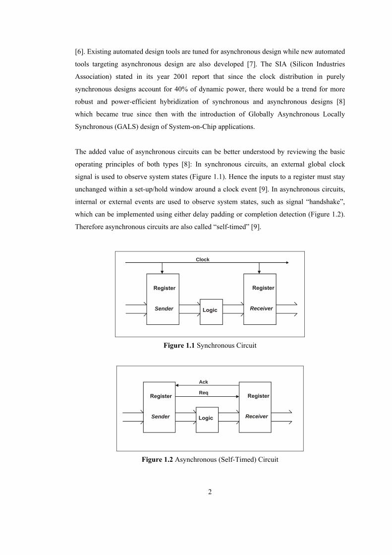
The added value of asynchronous circuits can be better understood by reviewing the basic
operating principles of both types [8]: In synchronous circuits, an external global clock
signal is used to observe system states (Figure 1.1). Hence the inputs to a register must stay
unchanged within a set-up/hold window around a clock event [9]. In asynchronous circuits,
internal or external events are used to observe system states, such as signal “handshake”,
which can be implemented using either delay padding or completion detection (Figure 1.2).
Therefore asynchronous circuits are also called “self-timed” [9].
Sender Receiver
Clock
Figure 1.1 Synchronous Circuit
Sender Receiver
Ack
Req
Figure 1.2 Asynchronous (Self-Timed) Circuit
3
1.1 Benefits of Asynchronous Design
Asynchronous systems greatly benefit from elimination of the global clock signal. The
following are the main advantages of asynchronous design:
(i) Elimination of clock network: In a synchronous system, the global clock signal must be
distributed evenly throughout the chip so that the clock event arrives at each register at the
same time to avoid clock skew. As feature sizes decrease and integration levels increase, the
clock distribution network in the circuit becomes more difficult to handle, requiring
extensive design effort, consuming silicon area and power [10]. Asynchronous systems use
local handshaking signals to regulate data transitions between stages instead of a global
clock. Elimination of clock signal also eliminates the clock distribution network and clock
skew considerations.
(ii) Low power consumption: In a synchronous system, all parts of the circuit are clocked
whether they are actually doing anything useful or not. The clock distribution network itself,
being constructed of large buffers, also consumes 30-40% of the total dynamic power on a
chip [8]. To introduce power-saving/idle-modes to synchronous circuits clock-gating or
clock-stopping techniques are applied but at the cost of increased design effort, complexity
and lots of other problems created at high clock rates. On the other hand, asynchronous
circuits inherently cease their switching activity when no transition occurs on data signals
and can go from idle to full activity instantaneously on the event of a data transition.
(iii) Average Case Performance instead of Worst: In a synchronous circuit, the slowest path
in the design determines the clock speed. This means that circuits in the critical path require
extra design effort and complexity to ensure the desired clock rates. Rather then being fixed
to operate at the worst-case rate, asynchronous systems are designed to sense the completion
of an evaluation before proceeding data to the next stage and hence they can operate at the
average-case speed.
(iv) Robustness to Environmental Variations: The delay through a circuit is affected by
variations in temperature, supply voltage and fabrication. Synchronous systems assume that
worst possible combination of these factors are present and adjust the clock rate accordingly.
On the other hand, most asynchronous systems sense completion detection and run as fast as
the current physical conditions allow [3].
4
(v) Easier Metastability Avoidance and Input Accommodation: When external signals,
which are by nature asynchronous, are fed into a synchronous circuit, they need to be
sampled by the active edge of the global clock signal to be synchronized to the circuit. For
proper sampling, external inputs must stay unchanged within a set-up/hold window around
active edge of the global clock signal. If they don’t, then metastability is experienced. With
proper precautions in circuit design metastability is resolved eventually but it may still last
for an unbounded amount of time, causing failures in functionality of synchronous circuits
which are always designed for bounded delays [11]. Meanwhile, asynchronous circuits do
not need synchronization of external signals, but wait indefinite amounts of time until the
inputs become available. So they accommodate inputs more gracefully.
(vi) Easier Technology Migration: Today’s industry demand for achieving fast time-to-
market dictates reducing the design cycle of an integrated circuit through implementation of
previously designed modules in various technologies during their lifetimes. As a result fast
migration of module designs from one technology to another is frequently required.
Asynchronous circuits with their robustness to physical conditions provide easier technology
mitigation possibilities than their synchronous counterparts whose timing closure is highly
related to technology dependent parameters.
(vii) Suitability for SOC Applications (Modularity, Scalability and Reusability): System-On-
Chips require accommodation of several blocks designed in different technologies and with
different constraints on a single chip. Migration of module designs from one technology to
another faces the problem of interfacing multiple clock domains and adjusting chip-level
timing constraints to module level circuit-timing constraints. Asynchronous designs
inherently have precisely specified interfaces which simplify their integration into larger
systems [3]. There is no need to worry about synchronization problems, clock phase
differences or clock skew at chip-level interconnect. The module design itself is independent
of the interface constraints and hence reusable and scalable as well.
(vii) Lower Electromagnetic Emission: In synchronous systems all activity in the circuit is
focused around the active edges of the global clock. This localization in time causes sharp
spikes in current consumption and large amounts of electromagnetic energy to be radiated at
the harmonics of the clock frequency [6]. This emission can make it difficult to deliver
enough current to the circuit at clock edges, to meet the EMC requirements and to operate
radio frequency circuits nearby as it happens in the case of wireless mobile applications. The
5
elimination of clock in asynchronous systems spreads out all circuit activity in time,
resulting in a broadband distributed electromagnetic emission and reduced interference to
nearby systems.
1.2 Difficulties of Asynchronous Design
With all the stated advantages, asynchronous systems are still not so widely adopted as
synchronous ones since they have their drawbacks as well. These are:
(i) Design Complexity: Synchronous systems work on the principle that every computing
stage completes its evaluation in less than the duration of clock period. Hence they are easily
designed by defining the combinational logic to compute a given function and dividing the
data path with registers to achieve the desired clock rate. On the other hand, asynchronous
circuits require extra hardware to allow each computing block to perform local
synchronizations with the blocks that it is passing its data to. Some design styles also
requires completion-detection circuitry as well. These increase the complexity of hardware
and in some cases also the silicon area.
(ii) Difficulty of Verification: In synchronous systems, by setting the clock period to a
reasonably long interval, all problems about dynamic behavior of the circuit are eliminated.
Verification consists of checking the logical functionality of combinatorial blocks and static
timing constraints imposed by the clock. However in asynchronous design, the dynamic
state of the circuit should be carefully analyzed to prevent hazards and critical races.
(iii) Reduced Testability: Synchronous designs are easily tested by using the scan-path
testing technique where the registers in the design act as latches of a single large shift-
register in scan-mode. Hence all registers in an integrated circuit can be brought to a desired
state and tested. Asynchronous circuits lack the deterministic behavior of state transitions in
clocked circuits, so it is much more difficult and not so straightforward to test them.
(iv) Poor Tool Support: Over the last three decades, all phases of the synchronous circuit
design process have been completely and successfully automated by CAD tools. These CAD
tools either need modifications for asynchronous design or do not apply to them at all. New
design tools for asynchronous circuit design are also developed but they are not so wide-
spread yet [7].
6
(v) Not well-known or well-thought: As synchronous systems have been dominating the
industry for years, designers are not familiar with asynchronous design methods and it’s
hard to break the habits. Besides, it is not as easy and as straightforward to grab the design
concepts when there is no clock to govern and synchronize all activities [1].
1.3 When to Use Asynchronous Design?
Both synchronous and asynchronous sequential circuits have their use in the design world,
depending on the requirements of the problem at hand. Rather than considering
asynchronous systems as a complete alternative to synchronous designs, it is usually
preferred to benefit from their advantages when synchronous methods fail or meet their
limitations. A most obvious example of when asynchronous design is preferable is
interfacing signals from outer world which are in fact asynchronous by nature [1]. In
synchronous circuits, interfacing external signals to a system clock is always subject to
meta-stability conditions where as, asynchronous circuits can be more gracefully interfaced
since they can wait as long as required, until the meta-stability resolves.
System-On-Chip (SoC) applications are another obvious application for asynchronous
circuits, where interconnections among different blocks within the chip constitute the
biggest design challenge. Synchronizing all blocks with one global clock is not practical,
especially when several blocks with different timing constraints are to be interfaced.
Improving the clock rate of the system could only be done at the cost of improving the
response time of each module. Implementing the chip-level interconnects asynchronously is
a widely preferred way of interfacing multiple clocked domains within the chip. System-On-
Chips designed in this manner are called Globally Asynchronous Locally Synchronous
(GALS). When a System-On-Chip is completely designed with asynchronous techniques
then it is called Globally Asynchronous Locally Asynchronous (GALA) [12].
1.4 Main Features of Asynchronous Circuits
Asynchronous designs operate on the self-timing principle where subsystems exchange
information at mutually negotiated times without external timing regulation. Data is passed
between modules through a group of wires known as the channel, which are usually
unidirectional point-to-point connections. The device that delivers data to the channel is
called the sender and the device that accepts data is called the receiver. The device that starts
7
the data transfer is called the initiator and the device responding to the initiator is called the
target [9].The presentation of essential issues in asynchronous design is based upon this
terminology.
1.4.1 Delay models
In asynchronous design, certain assumptions are made regarding the delays in gates and
wires within a circuit and the mode in which the circuit is operating. The unbounded delay
assumption, which ensures that a circuit will always function correctly under any
distribution of delay among the gates and wires within the circuit, is very convenient since it
separates the delay management from the functional correctness issue. However unbounded-
delay assumption is hard to realize in circuit design so there are many different delay models
in asynchronous design in addition to the unbounded-delay assumption [13]. The
classification of asynchronous design styles according to the delay models, which include
the timing assumptions and constraints on the circuit design, is as follows.
(i) Delay Insensitive: A circuit which conforms to the unbounded delay assumption, i.e.
which functions correctly irrespective of both gate and wire delays, is called delay-
insensitive [3]. For such circuits, no timing assumptions or constraints are required to ensure
functional correctness hence they offer the most reliable and robust self-timed operation
with the least amount of timing analysis effort. However delay-insensitive circuits are hard
to realize and in reality only a few types of circuits could confirm to this model.
(ii) Quasi-Delay Insensitive: These are similar to delay-insensitive circuits except that the
forks in wires are assumed to be isochronic, which means that difference between the signal
propagation delays in the branches of a set of interconnect wires is negligible with respect to
the delays of gates connected to these branches. This assumption is used when a signal is
demultiplexed to multiple targets: Unacknowledged forked signals are assumed to have
changed based on the observation at a single point on the fork.
(iii) Speed Independent: A circuit in which the wire delays are assumed to be negligible with
respect to gate delays is called speed-independent. Forks are assumed to be isochronic in
these circuits. This model is only applicable to small circuits or small portions of circuits [3].
8
1.4.2 Signaling and Handshaking Conventions
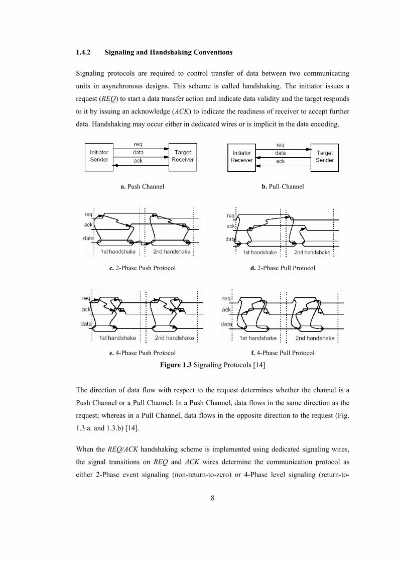
Signaling protocols are required to control transfer of data between two communicating
units in asynchronous designs. This scheme is called handshaking. The initiator issues a
request (REQ) to start a data transfer action and indicate data validity and the target responds
to it by issuing an acknowledge (ACK) to indicate the readiness of receiver to accept further
data. Handshaking may occur either in dedicated wires or is implicit in the data encoding.
a. Push Channel b. Pull-Channel
c. 2-Phase Push Protocol d. 2-Phase Pull Protocol
e. 4-Phase Push Protocol f. 4-Phase Pull Protocol
Figure 1.3 Signaling Protocols [14]
The direction of data flow with respect to the request determines whether the channel is a
Push Channel or a Pull Channel: In a Push Channel, data flows in the same direction as the
request; whereas in a Pull Channel, data flows in the opposite direction to the request (Fig.
1.3.a. and 1.3.b) [14].
When the REQ/ACK handshaking scheme is implemented using dedicated signaling wires,
the signal transitions on REQ and ACK wires determine the communication protocol as
either 2-Phase event signaling (non-return-to-zero) or 4-Phase level signaling (return-to-
9
zero). Of these two protocols, 4-Phase is easier to implement in CMOS digital circuits
(Figure 1.3.c., 1.3.d., 1.3.e. and 1.3.f.) [14].
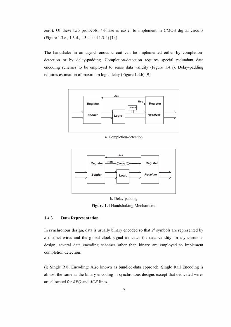
The handshake in an asynchronous circuit can be implemented either by completion-
detection or by delay-padding. Completion-detection requires special redundant data
encoding schemes to be employed to sense data validity (Figure 1.4.a). Delay-padding
requires estimation of maximum logic delay (Figure 1.4.b) [9].
Sender Receiver
Ack
Req
a. Completion-detection
Sender Receiver
Ack
ReqDelay
b. Delay-padding
Figure 1.4 Handshaking Mechanisms
1.4.3 Data Representation
In synchronous design, data is usually binary encoded so that 2n symbols are represented by
n distinct wires and the global clock signal indicates the data validity. In asynchronous
design, several data encoding schemes other than binary are employed to implement
completion detection:
(i) Single Rail Encoding: Also known as bundled-data approach, Single Rail Encoding is
almost the same as the binary encoding in synchronous designs except that dedicated wires
are allocated for REQ and ACK lines.
10
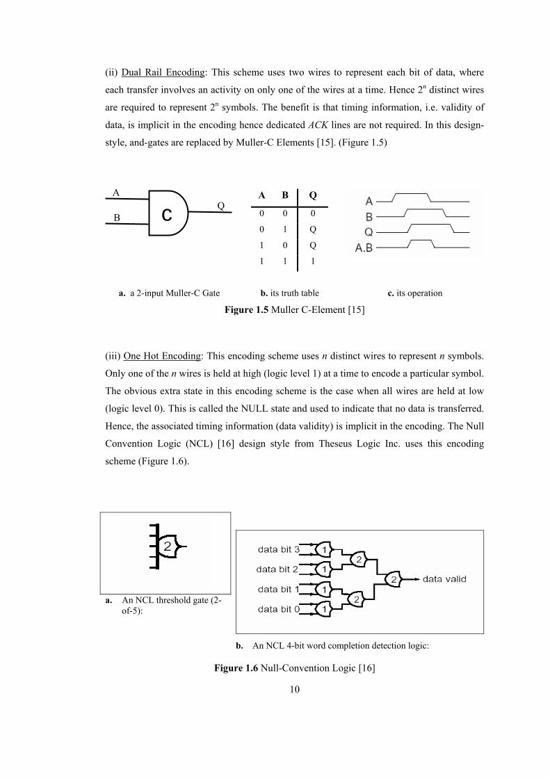
(ii) Dual Rail Encoding: This scheme uses two wires to represent each bit of data, where
each transfer involves an activity on only one of the wires at a time. Hence 2n distinct wires
are required to represent 2n symbols. The benefit is that timing information, i.e. validity of
data, is implicit in the encoding hence dedicated ACK lines are not required. In this design-
style, and-gates are replaced by Muller-C Elements [15]. (Figure 1.5)
A B Q
0 0 0
0 1 Q
1 0 Q
1 1 1
a. a 2-input Muller-C Gate b. its truth table c. its operation
Figure 1.5 Muller C-Element [15]
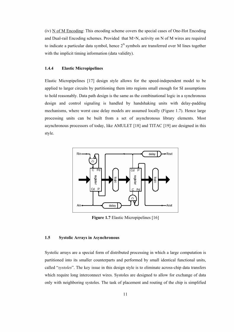
(iii) One Hot Encoding: This encoding scheme uses n distinct wires to represent n symbols.
Only one of the n wires is held at high (logic level 1) at a time to encode a particular symbol.
The obvious extra state in this encoding scheme is the case when all wires are held at low
(logic level 0). This is called the NULL state and used to indicate that no data is transferred.
Hence, the associated timing information (data validity) is implicit in the encoding. The Null
Convention Logic (NCL) [16] design style from Theseus Logic Inc. uses this encoding
scheme (Figure 1.6).
a. An NCL threshold gate (2-of-5):
b. An NCL 4-bit word completion detection logic:
Figure 1.6 Null-Convention Logic [16]
c A
B Q
11
(iv) N of M Encoding: This encoding scheme covers the special cases of One-Hot Encoding
and Dual-rail Encoding schemes. Provided that M>N, activity on N of M wires are required
to indicate a particular data symbol, hence 2N symbols are transferred over M lines together
with the implicit timing information (data validity).
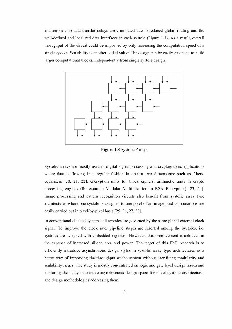
1.4.4 Elastic Micropipelines
Elastic Micropipelines [17] design style allows for the speed-independent model to be
applied to larger circuits by partitioning them into regions small enough for SI assumptions
to hold reasonably. Data path design is the same as the combinational logic in a synchronous
design and control signaling is handled by handshaking units with delay-padding
mechanisms, where worst case delay models are assumed locally (Figure 1.7). Hence large
processing units can be built from a set of asynchronous library elements. Most
asynchronous processors of today, like AMULET [18] and TITAC [19] are designed in this
style.
Figure 1.7 Elastic Micropipelines [16]
1.5 Systolic Arrays in Asynchronous
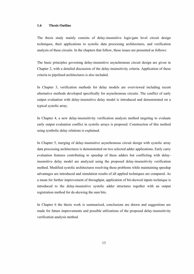
Systolic arrays are a special form of distributed processing in which a large computation is
partitioned into its smaller counterparts and performed by small identical functional units,
called “systoles”. The key issue in this design style is to eliminate across-chip data transfers
which require long interconnect wires. Systoles are designed to allow for exchange of data
only with neighboring systoles. The task of placement and routing of the chip is simplified
12
and across-chip data transfer delays are eliminated due to reduced global routing and the
well-defined and localized data interfaces in each systole (Figure 1.8). As a result, overall
throughput of the circuit could be improved by only increasing the computation speed of a
single systole. Scalability is another added value: The design can be easily extended to build
larger computational blocks, independently from single systole design.
Figure 1.8 Systolic Arrays
Systolic arrays are mostly used in digital signal processing and cryptographic applications
where data is flowing in a regular fashion in one or two dimensions; such as filters,
equalizers [20, 21, 22], encryption units for block ciphers, arithmetic units in crypto
processing engines (for example Modular Multiplication in RSA Encryption) [23, 24].
Image processing and pattern recognition circuits also benefit from systolic array type
architectures where one systole is assigned to one pixel of an image, and computations are
easily carried out in pixel-by-pixel basis [25, 26, 27, 28].
In conventional clocked systems, all systoles are governed by the same global external clock
signal. To improve the clock rate, pipeline stages are inserted among the systoles, i.e.
systoles are designed with embedded registers. However, this improvement is achieved at
the expense of increased silicon area and power. The target of this PhD research is to
efficiently introduce asynchronous design styles in systolic array type architectures as a
better way of improving the throughput of the system without sacrificing modularity and
scalability issues. The study is mostly concentrated on logic and gate level design issues and
exploring the delay insensitive asynchronous design space for novel systolic architectures
and design methodologies addressing them.
13
1.6 Thesis Outline
The thesis study mainly consists of delay-insensitive logic/gate level circuit design
techniques, their applications to systolic data processing architectures, and verification
analysis of these circuits. In the chapters that follow, these issues are presented as follows:
The basic principles governing delay-insensitive asynchronous circuit design are given in
Chapter 2, with a detailed discussion of the delay-insensitivity criteria. Application of these
criteria to pipelined architectures is also included.
In Chapter 3, verification methods for delay models are overviewed including recent
alternative methods developed specifically for asynchronous circuits. The conflict of early
output evaluation with delay-insensitive delay model is introduced and demonstrated on a
typical systolic array.
In Chapter 4, a new delay-insensitivity verification analysis method targeting to evaluate
early output evaluation conflict in systolic arrays is proposed. Construction of this method
using symbolic delay relations is explained.
In Chapter 5, merging of delay-insensitive asynchronous circuit design with systolic array
data processing architectures is demonstrated on two selected adder applications. Early carry
evaluation features contributing to speedup of these adders but conflicting with delay-
insensitive delay model are analyzed using the proposed delay-insensitivity verification
method. Modified systolic architectures resolving these problems while maintaining speedup
advantages are introduced and simulation results of all applied techniques are compared. As
a mean for further improvement of throughput, application of bit-skewed inputs technique is
introduced to the delay-insensitive systolic adder structures together with an output
registration method for de-skewing the sum bits.
In Chapter 6 the thesis work is summarized, conclusions are drawn and suggestions are
made for future improvements and possible utilizations of the proposed delay-insensitivity
verification analysis method.
14
Equation Chapter 2 Section 1 CHAPTER 2
2 DELAY INSENSITIVE ASYNCHRONOUS DESIGN
Delay-insensitivity is based on the assumption that “a circuit should function correctly
irrespective of all gate and interconnect delays as if these delays are unbounded” [3]. That’s
why delay-insensitive asynchronous circuits present a convenient alternative for designing in
deep-submicron, where interconnect delays have nearly equal effect on circuit behavior as
gate delays [29]. Delay-insensitive circuits offer robust self-timed operation with the least
amount of timing analysis effort available to asynchronous design styles: No global
constraints are required from the environment. Completion of each operation is
acknowledged to allow the environment to apply the next input, so the circuit can wait for
indefinite input arrival times and once the input arrives, can run as fast as the underlying
silicon technology allows [3]. Thus average case performance could be delivered by the
circuit instead of worst.
2.1 Delay Insensitive Design Styles
Delay-insensitive design style mainly falls into two categories according to the level of
abstraction applied [30]: Transistor -Level and Gate -Level.
Transistor-Level Delay-Insensitive Design Styles usually follow Martin’s methods [36] for
designing at transistor level and building optimized and usually state holding circuits
through formal transformations from logic descriptions. This design style produces the
circuits with minimum transistor count [37, 38], and has a specific language and design tool
developed for it [36], but due to its abstraction being at “transistor” level, not as widely
supported and automated as gate (logic) level design styles.
Gate-Level Delay-Insensitive Design Styles set the level of abstraction at logic design level,
provided that a standard cell library composed of special logic gates is used for circuit
implementation, either totally or partially, alongside with ordinary boolean logic. Such a
library contains logic elements which resemble the Muller C gates [31], in that they can hold
their states in case certain input conditions are not attained. These are called threshold-logic
15
gates, of which the most well-known and cooperated into an automated CAD flow is Null
Convention Logic (NCL) [16]. In gate-level delay-insensitive design mutually exclusive
symbol representations are used frequently instead of boolean representation, even though
boolean gates are still partially used. There is an increasing degree of automated tool support
for design and verification of gate-level design-insensitive circuits, due to their suitability for
system-on-chip design constraints.
2.2 Dual-Rail Threshold Logic Gates
True delay-insensitive circuits are very hard to realize, therefore very rare. However, being
the closest approximation, “Dual-rail Threshold Logic Gates” are widely referred as building
blocks for delay-insensitive circuits in literature. These circuits are actually “Quasi-delay
insensitive”, meaning that their functionality is based on the “isochronic forks” assumption
which states that all wiring works have equal delays, or at least those on small circuit scales.
Dual-rail Threshold Logic gates implement a logic function in case a certain input
conditions, namely the “threshold” are met, otherwise hold their states. They have been
developed concurrently under different names by different parties for gate-level delay-
insensitive design [33, 34, 35]. The most well known is the Null Convention Logic (NCL),
developed and commercialized by Theseus Logic Inc. in 1996, to address the delay-
insensitive asynchronous design space [16, 39, 40]. In NCL style, completion information is
not explicitly sent but embedded in data representation and circuits are constructed using all
gates from an NCL-type cell library. The basic principles characterizing the Dual-rail
Threshold Logic Gates are explained in the following subsections.
2.2.1 Symbolic Completeness of Expression
Symbolic Completeness of expression requires a logical expression to depend only on the
relationships of the symbols present, without a reference to the evaluation time [30]. Dual-
rail Threshold logic circuits use Mutually Exclusive Assertion Groups (MEAG), instead of
the Boolean Representation, to achieve Symbolic-Completeness of Expression. MEAGs
such as dual-rail signals eliminate the time reference by embedding control information into
data representation: A NULL or RESET value exists in the symbol set which is asserted
when data is not valid.
16
A dual-rail signal has two mutually exclusive data paths, D0 and D1, and implements three
logic states {NULL, DATA0, and DATA1} as given in Table 2.1. State DATA1 (D0 = 0
and D1 = 1) for Boolean logic 1, State DATA0 (D0 = 1 and D1 = 0) for Boolean logic 0 and
State NULL (D0 = 0 and D1 = 0) to indicate the result is not available yet. So the validity of
the output could be determined without a time reference. As the two rails are mutually
exclusive, (D0 = 1 and D1 = 1) is an illegal state.
Table 2.1 Dual Rail Signalling
STATES
SIGNALS
DATA0
(Boolean Logic 0)
DATA1
(Boolean Logic 1)
NULL
(Data not valid)
-
(undefined)
D0 1 0 0 1
D1 0 1 0 1
2.2.2 Two-Phase Operation
Dual-rail Threshold logic circuits are constructed from primitive modules known as
threshold gates with hysteresis [41]. A typical thmn gate, with 1 ≤ m ≤ n, has n inputs, of
which at least m of them has to become DATA for the output to assert a DATA value. This
is the “threshold” behavior. Similarly, at least m of the n inputs has to transition to NULL for
the output to assert NULL. Otherwise the threshold gate maintains its current state,
displaying “hysteresis” behavior. Specifically, a thmn gate functions like an n-input C-
element while a th1n gate like an n-input OR gate. Two typical gates from the Dual-rail
Threshold Logic Library and their truth tables are given in Figure 2.1.
a b c z
1 1 1 11 1 0 z1 0 1 z1 0 0 z0 1 1 z0 1 0 z0 0 1 z0 0 0 0
ath33b
cz
abc
zth13
a b c z
1 1 1 11 1 0 11 0 1 11 0 0 10 1 1 10 1 0 10 0 1 10 0 0 0
a. th33 gate with hysteresis b. th13 gate with hysteresis
Figure 2.1 Dual-rail Threshold logic style basic building gates
17
The threshold gates partition the inputs into separate NULL and DATA wavefronts, such
that a NULL value must be applied to the circuit inputs between consecutive DATA values,
so that the circuit always cycles between consecutive NULL and DATA inputs, eliminating
races and hazards completely.
2.2.3 Logic Design using Dual Rail Threshold Logic Gates
The most basic approach for logic design using Dual Rail Threshold Logic Gates is
producing a sum of minterms for both rails of the dual-rail output in DIMS (Delay
Insensitive Minterms Summation) style [32, 33], to implement the logic functionality. A
DIMS style full-adder built from dual-rail threshold logic gates is illustrated in Figure 2.2.
th14
th14
th14
th14
a1b1c1
a1b0c0
a0b1c0
a0b0c1
a0b0c0
a0b1c1
a1b0c1
a1b1c0
th33
th33
th33
th33
th33
th33
th33
th33
a1
a0
b1
b0
c1c0
Cout1
Cout0
Sum1
Sum0
Figure 2.2 DIMS Adder Structure built with Dual-Rail Threshold Logic Gates
There are other approaches which allow for some degree of boolean optimization and hence
do not require complete minterms but rely on C-gates to guarantee delay-insensitivity [34,
35].
18
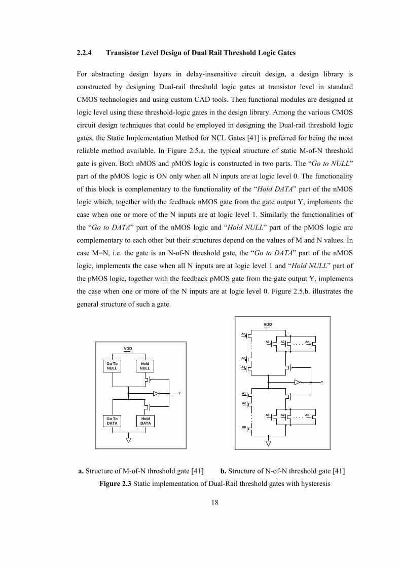
2.2.4 Transistor Level Design of Dual Rail Threshold Logic Gates
For abstracting design layers in delay-insensitive circuit design, a design library is
constructed by designing Dual-rail threshold logic gates at transistor level in standard
CMOS technologies and using custom CAD tools. Then functional modules are designed at
logic level using these threshold-logic gates in the design library. Among the various CMOS
circuit design techniques that could be employed in designing the Dual-rail threshold logic
gates, the Static Implementation Method for NCL Gates [41] is preferred for being the most
reliable method available. In Figure 2.5.a. the typical structure of static M-of-N threshold
gate is given. Both nMOS and pMOS logic is constructed in two parts. The “Go to NULL”
part of the pMOS logic is ON only when all N inputs are at logic level 0. The functionality
of this block is complementary to the functionality of the “Hold DATA” part of the nMOS
logic which, together with the feedback nMOS gate from the gate output Y, implements the
case when one or more of the N inputs are at logic level 1. Similarly the functionalities of
the “Go to DATA” part of the nMOS logic and “Hold NULL” part of the pMOS logic are
complementary to each other but their structures depend on the values of M and N values. In
case M=N, i.e. the gate is an N-of-N threshold gate, the “Go to DATA” part of the nMOS
logic, implements the case when all N inputs are at logic level 1 and “Hold NULL” part of
the pMOS logic, together with the feedback pMOS gate from the gate output Y, implements
the case when one or more of the N inputs are at logic level 0. Figure 2.5.b. illustrates the
general structure of such a gate.
Y
Go ToNULL
HoldNULL
VDD
Go ToDATA
HoldDATA
Y
VDD
A1
A1
A2
A2
An
An
A1 A2 An
A1 A2 An
a. Structure of M-of-N threshold gate [41] b. Structure of N-of-N threshold gate [41]
Figure 2.3 Static implementation of Dual-Rail threshold gates with hysteresis
19
After constructing a Dual-Rail Threshold gate according to the given Static Implementation
rules, further circuit optimizations could be employed to decrease the transistor count and
circuit area or to increase gate response times [30].
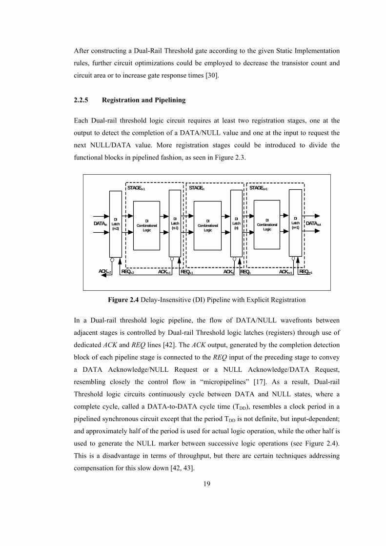
2.2.5 Registration and Pipelining
Each Dual-rail threshold logic circuit requires at least two registration stages, one at the
output to detect the completion of a DATA/NULL value and one at the input to request the
next NULL/DATA value. More registration stages could be introduced to divide the
functional blocks in pipelined fashion, as seen in Figure 2.3.
REQn+1
DATAin
REQn-1ACKn-2 ACKn
DI Latch (n+1)
DATAoutDI
Combinational Logic
DI Combinational
Logic
DI Combinational
Logic
DI Latch (n-2)
DI Latch(n-1)
DI Latch (n)
REQn-2 ACKn-1 REQn ACKn+1
STAGEn-1 STAGEn STAGEn+1
Figure 2.4 Delay-Insensitive (DI) Pipeline with Explicit Registration
In a Dual-rail threshold logic pipeline, the flow of DATA/NULL wavefronts between
adjacent stages is controlled by Dual-rail Threshold logic latches (registers) through use of
dedicated ACK and REQ lines [42]. The ACK output, generated by the completion detection
block of each pipeline stage is connected to the REQ input of the preceding stage to convey
a DATA Acknowledge/NULL Request or a NULL Acknowledge/DATA Request,
resembling closely the control flow in “micropipelines” [17]. As a result, Dual-rail
Threshold logic circuits continuously cycle between DATA and NULL states, where a
complete cycle, called a DATA-to-DATA cycle time (TDD), resembles a clock period in a
pipelined synchronous circuit except that the period TDD is not definite, but input-dependent;
and approximately half of the period is used for actual logic operation, while the other half is
used to generate the NULL marker between successive logic operations (see Figure 2.4).
This is a disadvantage in terms of throughput, but there are certain techniques addressing
compensation for this slow down [42, 43].
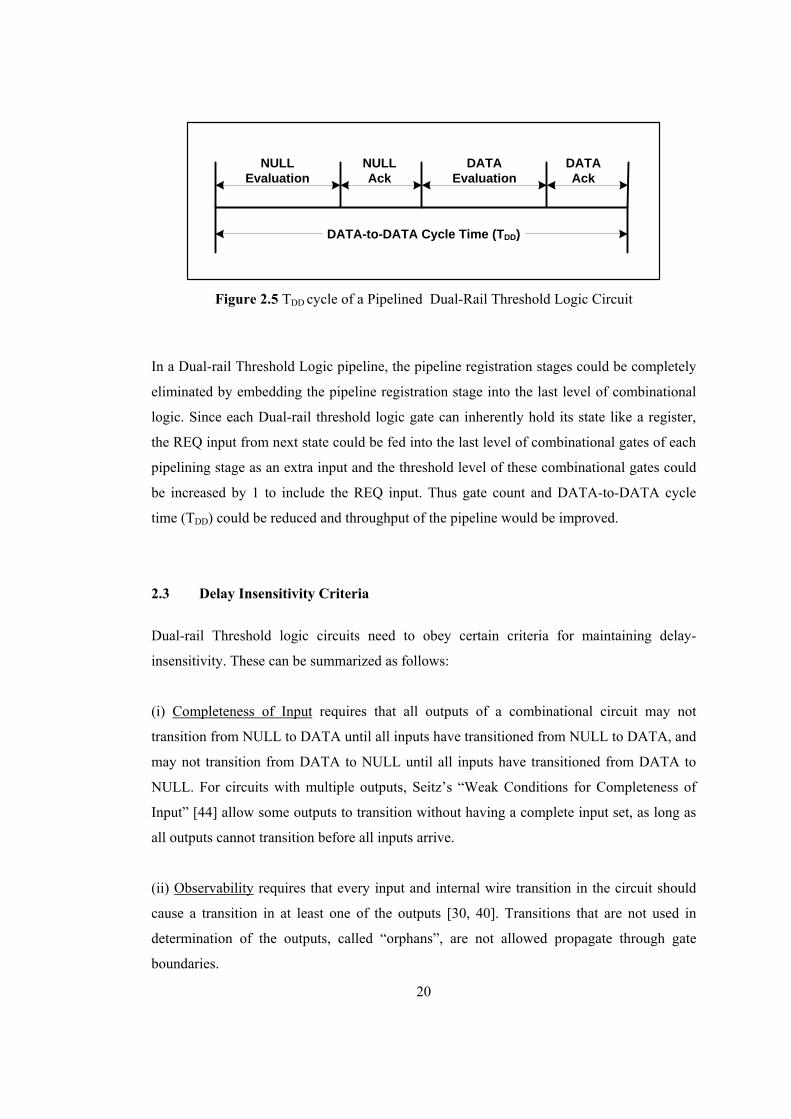
20
NULLEvaluation
DATAEvaluation
DATAAck
NULLAck
DATA-to-DATA Cycle Time (TDD)
Figure 2.5 TDD cycle of a Pipelined Dual-Rail Threshold Logic Circuit
In a Dual-rail Threshold Logic pipeline, the pipeline registration stages could be completely
eliminated by embedding the pipeline registration stage into the last level of combinational
logic. Since each Dual-rail threshold logic gate can inherently hold its state like a register,
the REQ input from next state could be fed into the last level of combinational gates of each
pipelining stage as an extra input and the threshold level of these combinational gates could
be increased by 1 to include the REQ input. Thus gate count and DATA-to-DATA cycle
time (TDD) could be reduced and throughput of the pipeline would be improved.
2.3 Delay Insensitivity Criteria
Dual-rail Threshold logic circuits need to obey certain criteria for maintaining delay-
insensitivity. These can be summarized as follows:
(i) Completeness of Input requires that all outputs of a combinational circuit may not
transition from NULL to DATA until all inputs have transitioned from NULL to DATA, and
may not transition from DATA to NULL until all inputs have transitioned from DATA to
NULL. For circuits with multiple outputs, Seitz’s “Weak Conditions for Completeness of
Input” [44] allow some outputs to transition without having a complete input set, as long as
all outputs cannot transition before all inputs arrive.
(ii) Observability requires that every input and internal wire transition in the circuit should
cause a transition in at least one of the outputs [30, 40]. Transitions that are not used in
determination of the outputs, called “orphans”, are not allowed propagate through gate
boundaries.
21
2.4 Pipelining Criteria
Dual-rail Threshold Logic circuits lend themselves easily to pipelining but pipelining
requires additional criterion to be obeyed for delay insensitivity. For maintaining proper
control flow in a pipelined Dual-rail Threshold Logic circuit, so that NULL and DATA
waves would not interact within a pipelining stage and violate delay insensitivity, the
evaluation time of ACK output of each pipelining stage should not be greater than arrival
time for REQ input to that pipelining stage, which is fed back from the next pipelining stage
as ACK output, as formulated in (1):
[ ] [ ] [ ] 1,,, +=≤ nnn ACKinputTimeREQinputTimeACKinputTime (1)
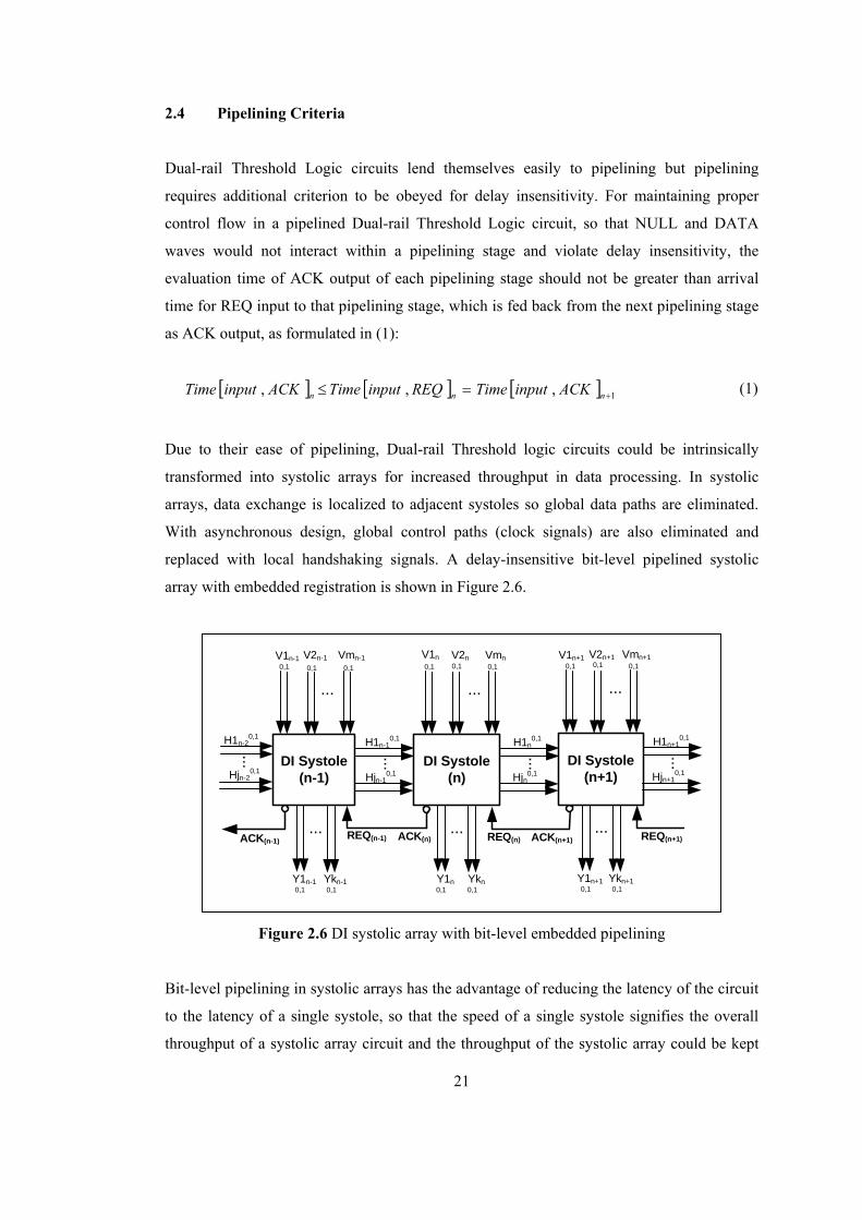
Due to their ease of pipelining, Dual-rail Threshold logic circuits could be intrinsically
transformed into systolic arrays for increased throughput in data processing. In systolic
arrays, data exchange is localized to adjacent systoles so global data paths are eliminated.
With asynchronous design, global control paths (clock signals) are also eliminated and
replaced with local handshaking signals. A delay-insensitive bit-level pipelined systolic
array with embedded registration is shown in Figure 2.6.
REQ(n) ACK(n+1) REQ(n+1)
Y1n-1 Ykn-1
REQ(n-1) ACK(n)
H1n-20,1
ACK(n-1)
DI Systole(n)
DI Systole(n+1)
DI Systole(n-1)
V1n-10,1
V2n-10,1
...
V1n0,1
V2n0,1
...
V1n+10,1
V2n+10,1
...
...
Vmn-10,1
Vmn0,1
Vmn+10,1
0,1 0,1Y1n Ykn
...
0,1 0,1Y1n+1 Ykn+1
...
0,1 0,1
Hjn-20,1
H1n-10,1
...
Hjn-10,1
H1n0,1
...
Hjn0,1
H1n+10,1
...
Hjn+10,1
...
Figure 2.6 DI systolic array with bit-level embedded pipelining
Bit-level pipelining in systolic arrays has the advantage of reducing the latency of the circuit
to the latency of a single systole, so that the speed of a single systole signifies the overall
throughput of a systolic array circuit and the throughput of the systolic array could be kept
22
constant against increasing array dimensions. But, with bit-level pipelining, an additional
criterion for delay insensitivity, called Completion Completeness [45], is introduced in case
bit-wise completion is used at registration stages and the combinational parts of the circuit
only conform to the Weak Condition for Completeness of Input
Completion Completeness is based on the fact that the dual-rail threshold logic registration
stage, which acknowledges either a DATA output or a NULL output, can only assure the
completeness of the output, not the completeness of input [45]. This may cause interaction
of consecutive DATA/NULL wavefronts and violate delay insensitive operation, when bit-
wise completion is adopted instead of word-wise completion for increasing the throughput
of the dual-rail threshold logic pipeline and the combinational parts only conform to the
Weak Condition for Completeness of Input. Since, in bit-wise completion, the completion
signal of each bit of the output is sent only to the dual-rail threshold logic registers that took
part in the calculation of that output bit. So an output bit does not reflect all input transitions
individually.
In case a dual-rail threshold logic registration stage is completion-incomplete, two methods
are proposed in [45] in order to ensure delay insensitivity: Either the topology of the
combinational blocks is modified to make all output bits input-complete or the completion
set of each register is modified to reflect input-completeness. However, these two methods
may conflict with logic level optimizations introduced for the purpose of decreasing the gate
count or increasing the evaluation speed. To preserve the advantages of logic level
optimizations while realizing completion-completeness in order to ensure delay-
insensitivity, alternative methods are required.
23
CHAPTER 3
3 VERIFICATION OF DELAY INSENSITIVITY
All asynchronous systems are designed using a delay-model assumption and no matter what
the chosen delay model is (delay-insensitive, quasi delay-insensitive or speed-independent)
the circuit should be verified to ensure that the chosen delay model really holds with actual
circuit delays and under all desired operating conditions enforced by the environment.
Employing the dual-rail threshold logic gates and following certain design rules do not
always guarantee delay-insensitivity in dual-rail threshold logic circuits [46]. Even though a
dual-rail threshold logic circuit correctly performs the logical function for which it has been
designed for, some input sets may exist for which it can still violate delay-insensitivity.
Generally, there is a tradeoff between reliable delay-insensitive operation and overall
performance of delay-insensitive circuits. The special logic gates and data representation
style cost increased gate counts and slower completion times. A strict commitment to delay
insensitivity constraints introduces more redundant logic. On the other hand, optimizations
at circuit level which require relaxation of delay-insensitivity constraints (like early output
evaluation) increase the verification cost of the circuit, which is already a tedious issue in
asynchronous circuit design, no matter what delay model is used or how the circuit is
designed. After every optimization phase, verification should be iterated as well.
Preferably, verification of delay-model should be at behavioral specification level, because
performing timing verification on an implemented circuit, i.e. at the end of design flow is
infeasible and tedious, requiring extensive simulations and timing analysis for all possible
inputs and all possible orderings of inputs.
3.1 Formal Verification Methods and State Explosion Problem
The most well-known and commonly used verification method at behavioral abstraction
level is formal analysis. The formal analysis methods for verification of delay-insensitivity
are generally based on exploration of reachable states [46]; hence address State Transition
Graph (STG) based design flows (Figure 3.1). However with increasing circuit sizes, the
number of states explodes exponentially and even with automated tools, formal analysis
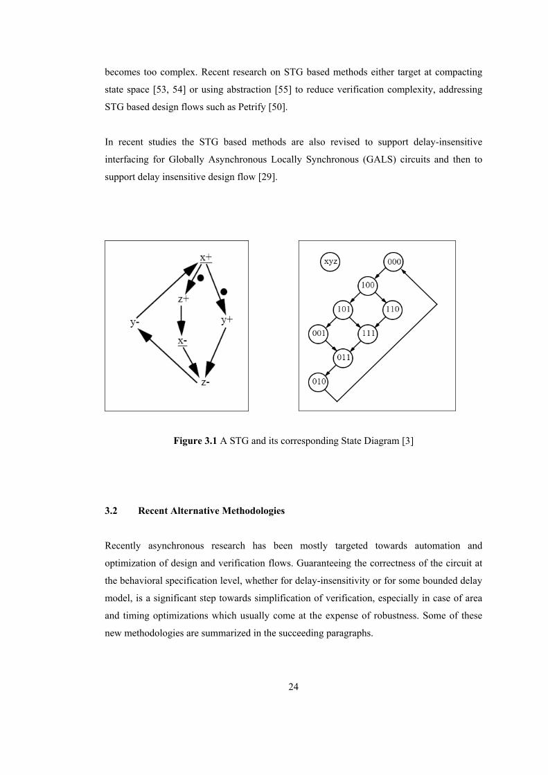
24
becomes too complex. Recent research on STG based methods either target at compacting
state space [53, 54] or using abstraction [55] to reduce verification complexity, addressing
STG based design flows such as Petrify [50].
In recent studies the STG based methods are also revised to support delay-insensitive
interfacing for Globally Asynchronous Locally Synchronous (GALS) circuits and then to
support delay insensitive design flow [29].
Figure 3.1 A STG and its corresponding State Diagram [3]
3.2 Recent Alternative Methodologies
Recently asynchronous research has been mostly targeted towards automation and
optimization of design and verification flows. Guaranteeing the correctness of the circuit at
the behavioral specification level, whether for delay-insensitivity or for some bounded delay
model, is a significant step towards simplification of verification, especially in case of area
and timing optimizations which usually come at the expense of robustness. Some of these
new methodologies are summarized in the succeeding paragraphs.
25
3.2.1 Relative Timing Assumptions
Relative Timing is an abstraction from exact timing constraints by considering relative
ordering of events with respect to each other instead of exact timing which is hard to know
at the beginning of a design flow [56]. “Difference” (event a fires earlier than event b) and
“Simultaneity” (event a and b fire at the same time with respect to event c) are examples of
Relative Timing Assumptions (RTA). By using RTA constraints, inconsistent event
sequences could be eliminated which in turn helps in compaction of reachable state space
and allow for optimizations in circuit design. This method has been both applied manually
[57, 58] and integrated into automated design flows in such a way that some of the relative
timing constraints could be generated from the circuit specification automatically [59, 60].
3.2.2 Lazy Transition Systems
The concept of “Laziness” was introduced in [56] to distinguish between the enabling and
firing of an event in a STG-based system. Using laziness concept, the concurrency of
transitions in an STG-based system could be increased or decreased, whichever is suitable
for the design simplification and optimization. Like RTA constraints, they allow for state
space reduction. This method has been successfully integrated in automated design flow
Petrify[59], so that Laziness could be detected and exploited automatically in generating and
backannotating RTA constraints [59] [60].
3.2.3 Symbolic Methods
Using symbolic and parametric delays instead of actual or relative timing constraints is
another method for timing abstraction, where actual delays of the circuit could only be
known after implementation. As introduced in [63] and [64], using unspecified timing
constraints represented as symbols, a set of linear constraints which guarantee the
correctness of timed transition systems could be generated and circuit optimizations could be
based on these models.
3.2.4 Partial Completion Methods with Early Evaluation
For automated design flows using dual-rail threshold logic gates such as NCL-X [51] [52],
there are recently proposed techniques for finding a compromise between circuit
26
optimization and reliable delay-insensitive operation. Early Evaluation and Partial
Completion Methods given in [61] and [62] respectively, both introduce relaxation of delay-
insensitivity constraints for dual-rail threshold circuits to allow for early evaluation of
signals so that more optimized and faster circuits could be synthesized without actually
violating delay-insensitivity constraints. This is achieved by distributing the early output
evaluation paths and gates which are to be relaxed and replaced with faster and smaller gates
in stead of NCL threshold gates within a complex combinational circuit in such a way that
the robustness of delay-insensitivity would not be diminished in the overall circuit and [61]
[62]. Both methods target to being embedded into automated NCL design flows. The method
in [61] also targets at gate-level simplifications as well as logic-level.
Partitioning a dual-rail threshold logic circuit into its control and data paths is another way to
reduce delay-insensitivity analysis complexity as proposed in [46], which tackles this
problem through orphan analysis. It assumes that DATA and NULL waves are properly
acknowledged at asynchronous registration stage, i.e. the cases of early generation or no
generation of completion acknowledgment are handled structurally, so it concentrates on
settling of all gates in the combinational network before acknowledgement is produced.
3.3 Early Outputs Conflict
Latency and throughput advantages of bit-level pipelining in dual-rail threshold logic
circuits could be easily outweighed by the slowness of threshold logic gates and the extra
NULL cycles. Speed-up is usually attained by introducing early evaluation of the signals,
propagating across the pipeline. However, early output evaluation implies allowing data-
dependent early execution where possible, i.e. by generating some circuit outputs, correctly,
without waiting for the arrival of all inputs, which directly conflicts with the two main
constraints of Delay-Insensitivity: When considered in terms of Input-Completeness, early
output evaluation implies input-incompleteness of early evaluated outputs. In terms of
Observability, the late arriving inputs, which are no longer required for generation of
outputs, create orphans, since their transitions would not affect the early outputs.
3.3.1 Early Output Evaluation vs. Delay Insensitivity
The Input-Completeness conflict could be solved by confirming to Seitz’s Weak Constraints
and Observability could be achieved by distributing the early output evaluation paths within
27
a complex combinational circuit in such a way that orphan-freedom could still be maintained
in the overall circuit [61] [62]. However, these solutions could not be directly applied to
systolic array style architectures since they evaluate only the combinational parts of the
circuit. Applying Seitz’s Weak Constraints for Input-completeness directly may violate the
Completion- Completeness requirement in bit-level pipelines. Meanwhile, commitment to
Completion- Completeness requirements would eliminate the speed-up advantages due to
early output evaluation. So, systolic array style delay-insensitive circuits, with bit-level
pipelining need specific solutions of their own.
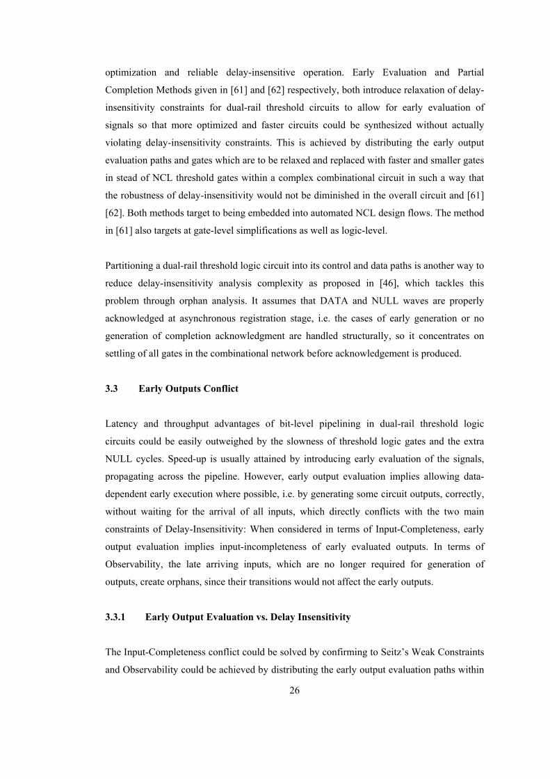
3.3.2 Demonstration on a Systolic Array
The initiating point for this study is the observation is that Delay-Insensitivity violations in a
systolic array with early output evaluation in one-dimension could be examined on three
adjacent systoles. This observation results from Spice simulations performed on gate level
implementations of dual-rail threshold logic systolic arrays, but could also be proposed
analytically: As each systole has data/control signal exchange with two neighboring systoles
in a one-dimensional systolic array, it is sufficient to analyze all signal transitions regarding
a single systole by considering the preceding and succeeding systoles in line. Therefore
analysis of three adjacent systoles in a one-dimensional systolic array is representative of the
behavior of all systoles in the array.
REQ(n) ACK(n+1) REQ(n+1)REQ(n-1) ACK(n)
Hn-20
ACK(n-1)
DI Systole(n)
DI Systole(n+1)
DI Systole(n-1)
V1n-10,1
V2n-10,1
V1n0,1
V2n0,1
...
V1n+10,1
V2n+10,1
...
Vmn-10,1
Vmn0,1
Vmn+10,1
Hn-21
...
Hn-10
Hn-11
Hn0
Hn1
Hn+10
Hn+11
Yn-10 Yn-1
1 Yn0 Yn
1 Yn+10Yn+1
1
Figure 3.2 DI systolic array with bit-level embedded pipelining
28
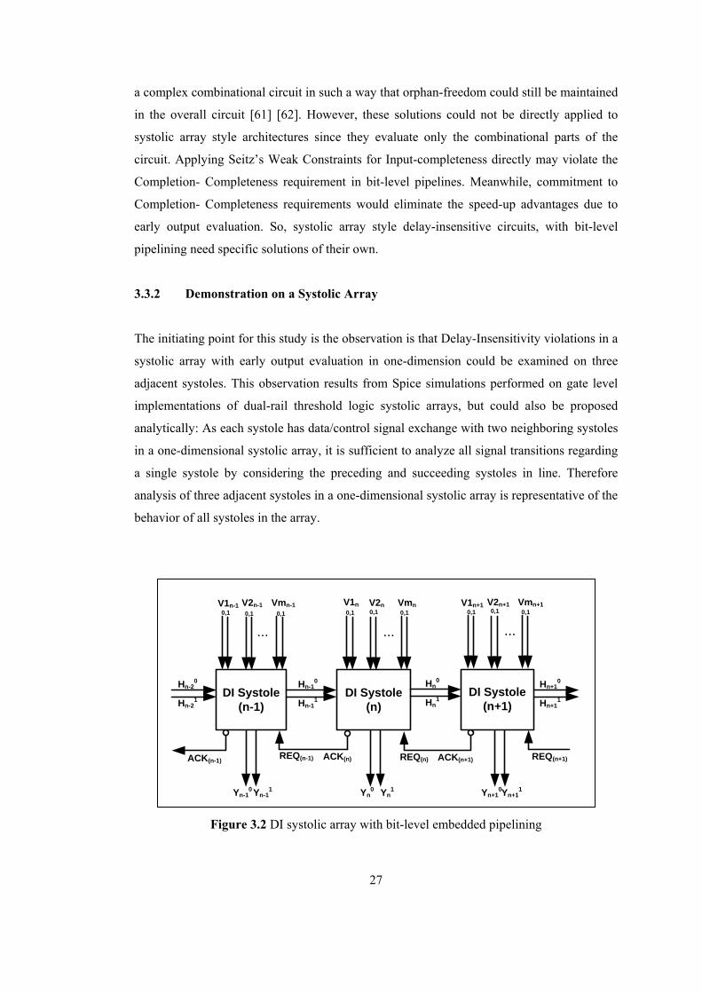
In Figure 3.2 a simplified version of the DI bit-level pipelined systolic array is given. For the
sake of simplicity, there is only one horizontal dual-rail output, which is propagated across
the pipeline, which may evaluate early (input-incomplete) or late (input-complete)
depending on the value of the vertical inputs to the pipeline. Also for the sake of simplicity,
there is only one vertical dual-rail output from each systole which is always input-complete.
The ACK outputs indicate completion detection of both vertical and horizontal outputs of
each systole. For this analysis it is assumed that all vertical inputs and the horizontal input to
the leftmost systole are applied concurrently to all systoles.
Then a typical delay-insensitivity violation scenario due to early output evaluation, which is
illustrated in Figure 3.3, through (a) to (d), runs as follows:
i) All inputs including the (n-1)th horizontal input are applied concurrently with
vertical inputs chosen such that, the nth and (n+1)th systoles evaluate early due to input-
incomplete horizontal outputs while the (n-1)th systole evaluates late due to input-complete
horizontal output (Fig. 3.3.a).
ii) The nth and (n+1)th systoles calculate early horizontal outputs concurrently since
they need not wait for evaluation of the horizontal output from the (n-1)th and nth systoles.
Evaluation of input-complete vertical output is triggered at the (n-+1)th systole by the arrival
of horizontal output from the nth systole (Fig. 3.3.b).
iii) The (n-1)th systole evaluates input-complete vertical output and late horizontal
output while the (n+1)th systole evaluates input-complete vertical output. Evaluation of
input-complete vertical output is triggered at the nth systole by the arrival of horizontal
output from the (n-1)th systole (Fig. 3.3.c).
iv) The (n+1)th systole asserts a Data Acknowledge transition on ACKn+1 output which
arrives as a Null Request to REQn input of the nth systole, but before input-complete vertical
output is evaluated at the nth systole. With REQn at Null Request level, the nth systole cannot
assert valid input-complete vertical output; hence the ACKn output can not make a Data
Acknowledge transition. As a result DATA and NULL wave fronts interact at the nth systole
and stall control signal flow (Fig. 3.3.d).
29
REQ(n) ACK(n+1) REQ(n+1)REQ(n-1) ACK(n)
Hn-20
ACK(n-1)
DI Systole(n)
DI Systole(n+1)
DI Systole(n-1)
V1n-10,1
V2n-10,1
V1n0,1
V2n0,1
...
V1n+10,1
V2n+10,1
...
Vmn-10,1
Vmn0,1
Vmn+10,1
Hn-21
...
Hn-10
Hn-11
Hn0
Hn1
Hn+10
Hn+11
Yn-10 Yn-1
1 Yn0 Yn
1 Yn+10Yn+1
1
(a)
REQ(n) ACK(n+1) REQ(n+1)REQ(n-1) ACK(n)
Hn-20
ACK(n-1)
DI Systole(n)
DI Systole(n+1)
DI Systole(n-1)
V1n-10,1
V2n-10,1
V1n0,1
V2n0,1
...
V1n+10,1
V2n+10,1
...
Vmn-10,1
Vmn0,1
Vmn+10,1
Hn-21
...
Hn-10
Hn-11
Hn0
Hn1
Hn+10
Hn+11
Yn-10 Yn-1
1 Yn0 Yn
1 Yn+10Yn+1
1
(b)
REQ(n) ACK(n+1) REQ(n+1)REQ(n-1) ACK(n)
Hn-20
ACK(n-1)
DI Systole(n)
DI Systole(n+1)
DI Systole(n-1)
V1n-10,1
V2n-10,1
V1n0,1
V2n0,1
...
V1n+10,1
V2n+10,1
...
Vmn-10,1
Vmn0,1
Vmn+10,1
Hn-21
...
Hn-10
Hn-11
Hn0
Hn1
Hn+10
Hn+11
Yn-10Yn-1
1 Yn0 Yn
1 Yn+10Yn+1
1
(c)
Figure 3.3 Signal flow for a delay-insensitivity violation scenario
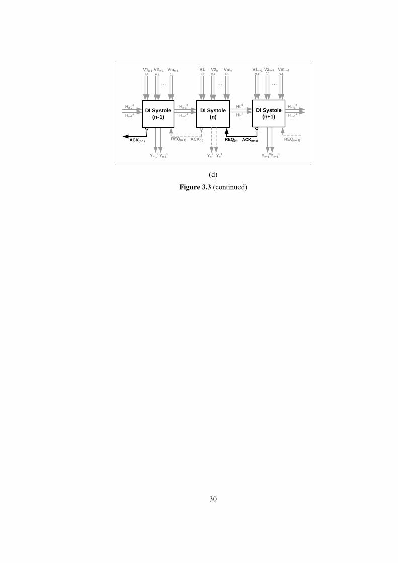
30
REQ(n) ACK(n+1) REQ(n+1)REQ(n-1) ACK(n)
Hn-20
ACK(n-1)
DI Systole(n)
DI Systole(n+1)
DI Systole(n-1)
V1n-10,1
V2n-10,1
V1n0,1
V2n0,1
...
V1n+10,1
V2n+10,1
...
Vmn-10,1
Vmn0,1
Vmn+10,1
Hn-21
...
Hn-10
Hn-11
Hn0
Hn1
Hn+10
Hn+11
Yn-10 Yn-1
1 Yn0 Yn
1 Yn+10Yn+1
1
(d)
Figure 3.3 (continued)
31
Equation Chapter 3 Section 1Equation Chapter 4 Section 1
CHAPTER 4
4 DELAY-INSENSITIVITY VERIFICATION METHOD FOR SYSTOLIC ARRAYS
For improving the performance of delay-insensitive circuits at structural level, pipelining
methods and systolic-array architectures are introduced. However, the speed improvement
achieved by pipelining in terms of throughput and latency is usually outweighed by the extra
“reset phases”, which have to be inserted in between consecutive computations (“set
phases”) to correctly operate delay-insensitive pipelines [3]. In order to make the delay-
insensitive pipelines fast enough to achieve the average case performance which is
theoretically expected of them, data-dependent early output evaluation is allowed by
relaxing the delay-insensitivity constraints. But relaxation of delay-insensitivity constraints
(like early output evaluation) increase the verification cost of the circuit, which is already a
tedious issue in asynchronous circuit design, no matter what delay model is used or how the
circuit is designed.
To detect input-dependent delay-insensitivity violations in systolic dual-rail threshold logic
adders, running extensive simulations covering all possible inputs is not a feasible option,
especially for large operand sizes. The formal analysis methods for verification of delay-
insensitivity, which are based on exploration of reachable states, usually suffer from the state
explosion problem; hence reducing the verification complexity is an important step in
simplifying the design cycle. A structural delay-insensitivity analysis and verification
method is introduced for asynchronous pipelines, designed in dual-rail threshold logic style.
The proposed method, which is abbreviated as the SDIVA (Structural Delay-Insensitivity
Analysis And Verification) method, targets at maintaining delay-insensitivity of bit-level
pipelined systolic array style structures where speed up is achieved by data-dependent early
output evaluations in one-dimension and where it is safe to assume that all wiring forks
within each systole are isochronic. Using symbolic delays for output evaluation times
without imposing any timing assumptions on the environment, all possible data-dependent
early/late output evaluation cases are examined by concentrating on only three adjacent bit
systoles. This way, input sets causing delay-insensitivity violations are detected and
corrected without diminishing the speed up advantages of early output evaluation feature.
32
4.1 Structural Delay Insensitivity Verification Analysis Method (SDIVA)
The analysis carried out on systolic arrays with bit-level pipelining (presented in Chapter 3),
shows that delay-insensitivity violations due to early output evaluation could be simplified
down to interaction of three adjacent systoles. Since systolic arrays are constructed from
identical systoles, i.e. units with identical functionality hence identical implementation and
identical delays, then an analysis method which simplifies the verification task to the
analysis of the eight possible Early/Late output evaluation scenarios
{Early, Early, Early},
{Early, Early, Late},
{Early, Late, Early},
{Early, Late, Late},
{Late, Early, Early},
{Late, Early, Late},
{Late, Late, Early},
{Late, Late, Late}
on three adjacent systoles could be constructed.
4.1.1 Symbolic Delay Assignment
On the simplified bit-level pipelined systolic array example given in Figure 4.1, where the
single horizontal output may follow two different evaluation paths as early and late
depending on the applied inputs, delays of all output paths could be represented with the
following symbolic values, such that each symbolic delay value represents sum of all gate
and wiring delays on that evaluation path:
dHE delay of the horizontal output path in case of early evaluation (input-incomplete)
dHL: delay of the horizontal output path in case of late evaluation (input-complete)
dV delay of the vertical output path (input-complete)
dA delay of the completion detection path, ACK, (input-complete)
Note that early evaluation of the horizontal output indicates evaluation of the horizontal
output using the vertical systole inputs only, i.e. without waiting for the arrival of the
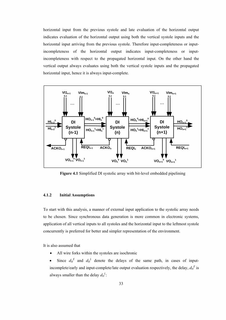
33
horizontal input from the previous systole and late evaluation of the horizontal output
indicates evaluation of the horizontal output using both the vertical systole inputs and the
horizontal input arriving from the previous systole. Therefore input-completeness or input-
incompleteness of the horizontal output indicates input-completeness or input-
incompleteness with respect to the propagated horizontal input. On the other hand the
vertical output always evaluates using both the vertical systole inputs and the propagated
horizontal input, hence it is always input-complete.
REQIn ACKOn+1 REQIn+1REQIn-1 ACKOn
HIn-20
ACKOn-1
DI Systole
(n)
DI Systole
(n+1)
DI Systole
(n-1)
VI1n-10,1
VI1n0,1
...
VI1n+10,1
...
VImn-10,1
VImn0,1
VImn+10,1
HIn-21
...
HOn-10=HIn0
HOn+10
HOn+11
VOn-10 VOn-1
1VOn
0 VOn1 VOn+1
0 VOn+11
HOn-11=HIn1
HOn0=HIn+1
0
HOn1=HIn+1
1
Figure 4.1 Simplified DI systolic array with bit-level embedded pipelining
4.1.2 Initial Assumptions
To start with this analysis, a manner of external input application to the systolic array needs
to be chosen. Since synchronous data generation is more common in electronic systems,
application of all vertical inputs to all systoles and the horizontal input to the leftmost systole
concurrently is preferred for better and simpler representation of the environment.
It is also assumed that
• All wire forks within the systoles are isochronic
• Since dHE and dH
L denote the delays of the same path, in cases of input-
incomplete/early and input-complete/late output evaluation respectively, the delay, dHE is
always smaller than the delay dHL:
34
L
HE
H dd < (2)
To continue with this analysis, there is no need to make any other assumptions regarding the
relational magnitudes of the symbolic delays with respect to each other. The relation given
in (2), does not impose any timing constraints on the systole design either, hence it does not
challenge the definition of delay-insensitivity So it could be safely stated that no timing
constraints are imposed on the circuit structure to maintain delay-insensitivity by these
assumptions.
4.1.3 Analysis with Symbolic Delays
For all of the possible eight Early/Late carry output scenarios, evaluation time of ACK
outputs from the time of inputs’ application is calculated in terms of the symbolic delays, dV,
dA, dHE, dH
L, and presented in Tables 4.1 to 4.8. In these tables, the following abbreviations
are used:
HI : Horizontal Input,
HO: : Horizontal Output,
VI : Vertical Input,
VO : Vertical Output,
ACKO : Completion Detection Output
REQI : Request Input.
The ACKO evaluation time of each systole is then compared to evaluation time of the REQI
input to that systole, which is actually the to ACKO output of the next systole, in order to
check if the DI Pipelining Constraint, formulated in the relation (1) on page 21 is satisfied.
In these comparisons, only the relation formulated in (2) is used and thus the input scenarios
which violate the delay-insensitive pipelining constraint are detected.
In calculation of the evaluation delays, the following formulas are applied to each systole
which is enforced by the structure of the pipeline:
HIn= HOn-1 (3)
VOn =HIn + dV (4)
ACKOn= Max{HO n, VO n}+ dA (5)
REQI n= ACKOn+1 (6)
35
Note that the pipelining constraint is checked for the nth systole and (n-1)th systole only. The
calculations on the (n+1)th systole only serve for calculating the evaluation time of the REQI
input to the nth systole.
Examining the Tables 4.1 to 4.8 reveals that for the input scenarios {Late, Early, Early} and
{Late, Early, Late}, DI Pipelining Constraint is violated as indicated by the bold lettering in
Table 4.5 and Table 4.6. and satisfied for all other scenarios as stated below:
{Early, Early, Early}, DI Pipelining Constraint is satisfied √
{Early, Early, Late}, DI Pipelining Constraint is satisfied√
{Early, Late, Early}, DI Pipelining Constraint is satisfied √
{Early, Late, Late}, DI Pipelining Constraint is satisfied√
{Late, Early, Early}, DI Pipelining Constraint is violated !
{Late, Early, Late}, DI Pipelining Constraint is violated !
{Late, Late, Early}, DI Pipelining Constraint is satisfied √
{Late, Late, Late} DI Pipelining Constraint is satisfied√
For the input scenario {Late, Early, Early}, the evaluation time for the ACKO output of nth
systole is definitely smaller than the evaluation time for ACKO output of the (n+1) th systole,
which is also the REQI input arrival time for nth systole. For the input scenario{Late, Early,
Late}, given in Table 4.6, a violation of DI Pipelining Constraint is inferred in case the late
evaluation time of the horizontal output dHL is greater than the evaluation time of the vertical
output dV or in case the evaluation time of the vertical output dV is smaller than the late
evaluation time of the horizontal output dHL but greater than the early evaluation time of the
horizontal output dHE. In both scenarios, the result is NULL and DATA waves within the nth
systole, leading to no generation of the ACKO output and blocking of signal flow.
Another important revelation of the examinations carried on Tables 4.1 to 4.8 is that, in a
bit-level pipelined systolic array in dual-rail threshold logic style, which has early and late
output evaluation paths in one-dimension, out of the eight possible scenarios, the analysis of
only two scenarios {Late, Early, Early} and {Late, Early, Late} on three adjacent systoles is
sufficient for verification of delay-insensitivity.
36
Table 4.1 DI Systole in case of { Early, Early, Early } Scenario
Systole/ Scenario
Input/Output Signal Evaluation Time
HIn-1 0
HOn-1 (early) dHE
VOn-1 =HIn-1 + dV dV
ACKOn-1= Max{HO n-1, VO n-1}+ dA Max{dHE, dV}+dA
n-1 (Early)
REQI n-1= ACKOn dHE + dV + dA
HIn= HOn-1 (early) dHE
HOn (early) dHE
VOn =HIn + dV dHE + dV
ACKOn= Max{HO n, VO n}+ dA Max{ dHE, dH
E+dV }+dA = dHE+dV +dA
n (Early)
REQI n= ACKOn+1 dHE+dV+dA
HIn+1= HOn (early) dHE
HOn+1 (early) dHE
VOn+1 =HIn+1 + dV dHE+dV
ACKOn+1= Max{HO n+1, VO n+1}+ dA Max{ dHE, dH
E+dV }+dA = dHE+dV+dA
n+1 (Early)
REQI n+1= ACKOn+2 …
(i) Examination of Pipelining Constraints for {Early, Early, Early} Scenario
DI Systole (n-1):
If dHE>dV then
ACKOn-1= dHE +dA and REQI n-1= dH
E + dV + dA > dHE +dA
If dHE< dV then
ACKOn-1= dV +dA and REQI n-1= dHE + dV + dA > dV+dA
Since REQI n-1 = ACKOn ≥ ACKOn-1 , DI Pipelining Constraint is satisfied √
DI Systole (n):
Since dHE + dV > dH
E
ACKOn= dHE + dV + dA = REQI n
Since REQI n = ACKOn+1 ≥ ACKOn , DI Pipelining Constraint is satisfied √
37
Table 4.2 DI Systole in case of { Early, Early, Late } Scenario
Systole/ Scenario
Input/Output Signal Evaluation Time
HIn-1 0
HOn-1 (early) dHE
VOn-1 =HIn-1 + dV dV.
ACKOn-1= Max{HO n-1, VO n-1}+ dA Max{ dHE,dV}+dA
n-1 (Early)
REQI n-1= ACKOn dHE+dV+dA
HIn= HOn-1 (early) dHE
HOn (early) dHE
VOn =HIn + dV dHE+dV
ACKOn= Max{HO n, VO n}+ dA Max{ dHE,dH
E+dV }+dA = dHE+dV+dA
n (Early)
REQI n= ACKOn+1 Max{ dHE+dH
L,dHE+dV }+dA
HIn+1= HOn (early) dHE
HOn+1 (late) dHE+dH
L
VOn+1 =HIn+1 + dV dHE+dV
ACKOn+1= Max{HO n+1, VO n+1}+ dA Max{ dHE+dH
L,dHE+dV }+dA
n+1 (Late)
REQI n+1= ACKOn+2 …
(ii) Examination of Pipelining Constraints for {Early, Early, Late} Scenario
DI Systole (n-1):
If dHE>dV then
ACKOn-1= dHE + dA and REQI n-1= dH
E + dV + dA > dHE +dA
If dHE< dV then
ACKOn-1= dV + dA and REQI n-1= dHE + dV + dA > dV +dA
Since REQI n-1 = ACKOn ≥ ACKOn-1 , DI Pipelining Constraint is satisfied √
DI Systole (n):
Since dHE + dV > dH
E
ACKOn= dHE + dV + dA
If dHL>dV then
REQI n= dHE + dH
L + dA > dHE + dV + dA =ACKOn
If dHL < dV then
REQI n= dHE + dV + dA and dH
E + dV + dA = ACKOn
Since REQI n = ACKOn+1 ≥ ACKOn , DI Pipelining Constraint is satisfied √
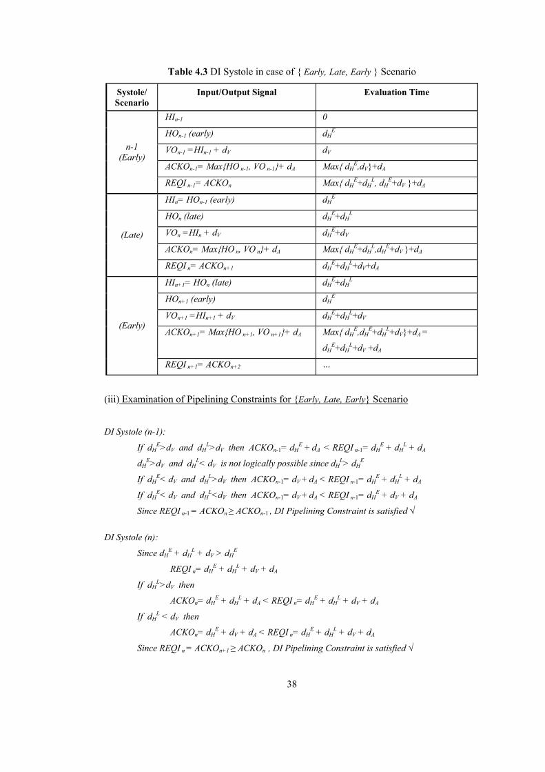
38
Table 4.3 DI Systole in case of { Early, Late, Early } Scenario
Systole/ Scenario
Input/Output Signal Evaluation Time
HIn-1 0
HOn-1 (early) dHE
VOn-1 =HIn-1 + dV dV
ACKOn-1= Max{HO n-1, VO n-1}+ dA Max{ dHE,dV}+dA
n-1 (Early)
REQI n-1= ACKOn Max{ dHE+dH
L, dHE+dV }+dA
HIn= HOn-1 (early) dHE
HOn (late) dHE+dH
L
VOn =HIn + dV dHE+dV
ACKOn= Max{HO n, VO n}+ dA Max{ dHE+dH
L,dHE+dV }+dA
(Late)
REQI n= ACKOn+1 dHE+dH
L+dV+dA
HIn+1= HOn (late) dHE+dH
L
HOn+1 (early) dHE
VOn+1 =HIn+1 + dV dHE+dH
L+dV
ACKOn+1= Max{HO n+1, VO n+1}+ dA Max{ dHE,dH
E+dHL+dV}+dA =
dHE+dH
L+dV +dA
(Early)
REQI n+1= ACKOn+2 …
(iii) Examination of Pipelining Constraints for {Early, Late, Early} Scenario
DI Systole (n-1):
If dHE>dV and dH
L>dV then ACKOn-1= dHE + dA < REQI n-1= dH
E + dHL + dA
dHE>dV and dH
L< dV is not logically possible since dHL> dH
E
If dHE< dV and dH
L>dV then ACKOn-1= dV + dA < REQI n-1= dHE + dH
L + dA
If dHE< dV and dH
L<dV then ACKOn-1= dV + dA < REQI n-1= dHE + dV + dA
Since REQI n-1 = ACKOn ≥ ACKOn-1 , DI Pipelining Constraint is satisfied √
DI Systole (n):
Since dHE + dH
L + dV > dHE
REQI n= dHE + dH
L + dV + dA
If dHL>dV then
ACKOn= dHE + dH
L + dA < REQI n= dHE + dH
L + dV + dA
If dHL < dV then
ACKOn= dHE + dV + dA < REQI n= dH
E + dHL + dV + dA
Since REQI n = ACKOn+1 ≥ ACKOn , DI Pipelining Constraint is satisfied √
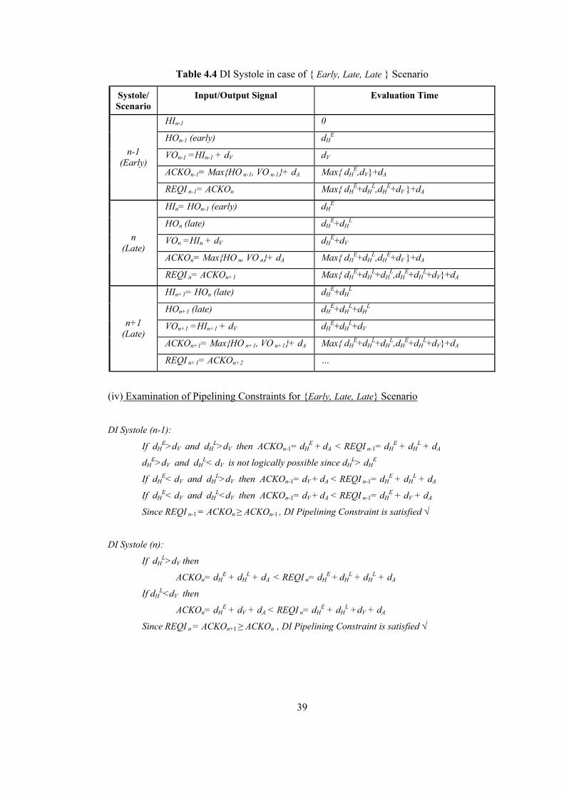
39
Table 4.4 DI Systole in case of { Early, Late, Late } Scenario
Systole/ Scenario
Input/Output Signal Evaluation Time
HIn-1 0
HOn-1 (early) dHE
VOn-1 =HIn-1 + dV dV
ACKOn-1= Max{HO n-1, VO n-1}+ dA Max{ dHE,dV}+dA
n-1 (Early)
REQI n-1= ACKOn Max{ dHE+dH
L,dHE+dV }+dA
HIn= HOn-1 (early) dHE
HOn (late) dHE+dH
L
VOn =HIn + dV dHE+dV
ACKOn= Max{HO n, VO n}+ dA Max{ dHE+dH
L,dHE+dV }+dA
n (Late)
REQI n= ACKOn+1 Max{ dHE+dH
L+dHL,dH
E+dHL+dV}+dA
HIn+1= HOn (late) dHE+dH
L
HOn+1 (late) dHE+dH
L+dHL
VOn+1 =HIn+1 + dV dHE+dH
L+dV
ACKOn+1= Max{HO n+1, VO n+1}+ dA Max{ dHE+dH
L+dHL,dH
E+dHL+dV}+dA
n+1 (Late)
REQI n+1= ACKOn+2 …
(iv) Examination of Pipelining Constraints for {Early, Late, Late} Scenario
DI Systole (n-1):
If dHE>dV and dH
L>dV then ACKOn-1= dHE + dA < REQI n-1= dH
E + dHL + dA
dHE>dV and dH
L< dV is not logically possible since dHL> dH
E
If dHE< dV and dH
L>dV then ACKOn-1= dV + dA < REQI n-1= dHE + dH
L + dA
If dHE< dV and dH
L<dV then ACKOn-1= dV + dA < REQI n-1= dHE + dV + dA
Since REQI n-1 = ACKOn ≥ ACKOn-1 , DI Pipelining Constraint is satisfied √
DI Systole (n):
If dHL>dV then
ACKOn= dHE + dH
L + dA < REQI n= dHE + dH
L + dHL + dA
If dHL<dV then
ACKOn= dHE + dV + dA < REQI n= dH
E + dHL +dV + dA
Since REQI n = ACKOn+1 ≥ ACKOn , DI Pipelining Constraint is satisfied √
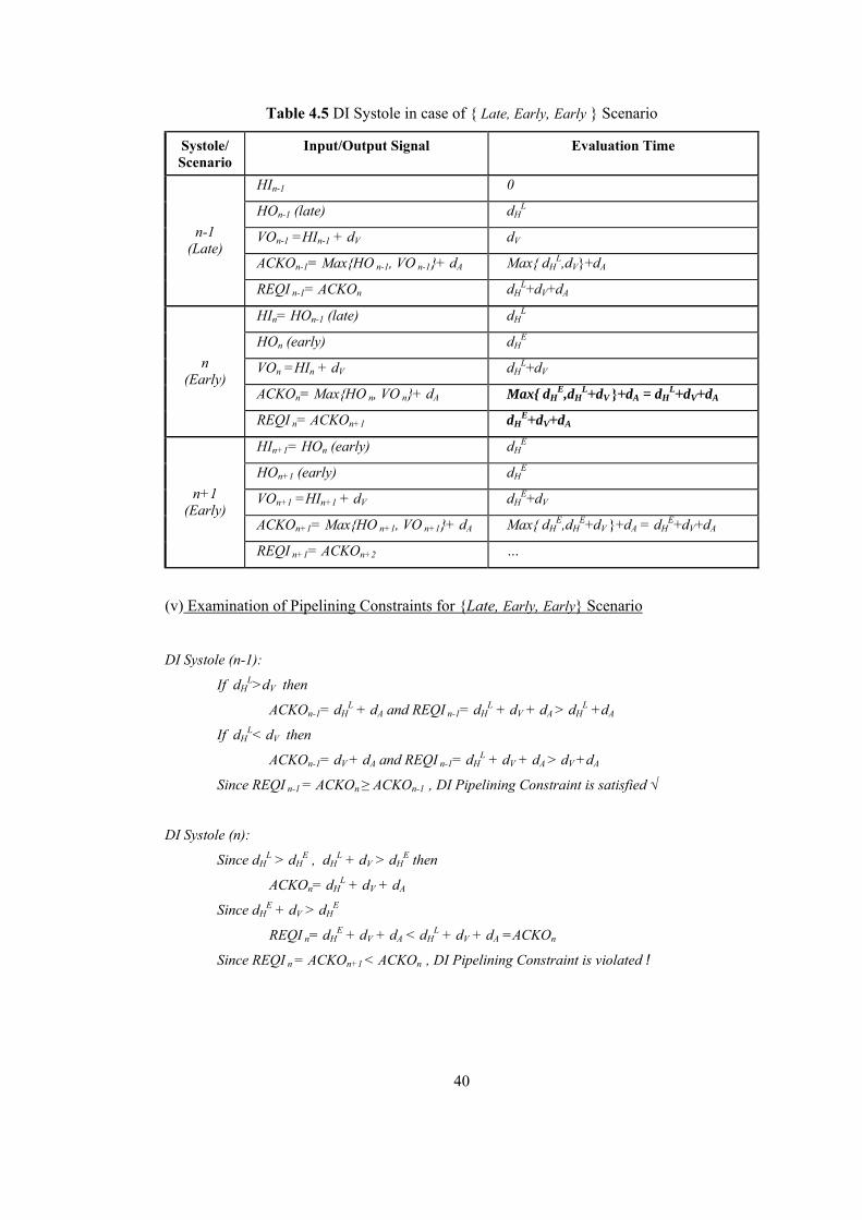
40
Table 4.5 DI Systole in case of { Late, Early, Early } Scenario
Systole/ Scenario
Input/Output Signal Evaluation Time
HIn-1 0
HOn-1 (late) dHL
VOn-1 =HIn-1 + dV dV
ACKOn-1= Max{HO n-1, VO n-1}+ dA Max{ dHL,dV}+dA
n-1 (Late)
REQI n-1= ACKOn dHL+dV+dA
HIn= HOn-1 (late) dHL
HOn (early) dHE
VOn =HIn + dV dHL+dV
ACKOn= Max{HO n, VO n}+ dA Max{ dHE,dH
L+dV }+dA = dHL+dV+dA
n (Early)
REQI n= ACKOn+1 dHE+dV+dA
HIn+1= HOn (early) dHE
HOn+1 (early) dHE
VOn+1 =HIn+1 + dV dHE+dV
ACKOn+1= Max{HO n+1, VO n+1}+ dA Max{ dHE,dH
E+dV }+dA = dHE+dV+dA
n+1 (Early)
REQI n+1= ACKOn+2 …
(v) Examination of Pipelining Constraints for {Late, Early, Early} Scenario
DI Systole (n-1):
If dHL>dV then
ACKOn-1= dHL + dA and REQI n-1= dH
L + dV + dA > dHL +dA
If dHL< dV then
ACKOn-1= dV + dA and REQI n-1= dHL + dV + dA > dV +dA
Since REQI n-1 = ACKOn ≥ ACKOn-1 , DI Pipelining Constraint is satisfied √
DI Systole (n):
Since dHL > dH
E , dHL + dV > dH
E then
ACKOn= dHL + dV + dA
Since dHE + dV > dH
E
REQI n= dHE + dV + dA < dH
L + dV + dA =ACKOn
Since REQI n = ACKOn+1 < ACKOn , DI Pipelining Constraint is violated !
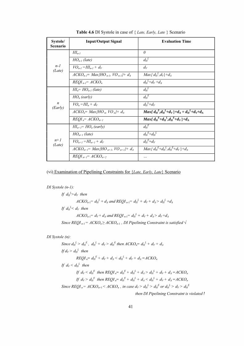
41
Table 4.6 DI Systole in case of { Late, Early, Late } Scenario
Systole/ Scenario
Input/Output Signal Evaluation Time
HIn-1 0
HOn-1 (late) dHL
VOn-1 =HIn-1 + dV dV
ACKOn-1= Max{HO n-1, VO n-1}+ dA Max{ dHL,dV}+dA
n-1 (Late)
REQI n-1= ACKOn dHL+dV +dA
HIn= HOn-1 (late) dHL
HOn (early) dHE
VOn =HIn + dV dHL+dV
ACKOn= Max{HO n, VO n}+ dA Max{ dHE,dH
L+dV }+dA = dHL+dV+dA
n (Early)
REQI n= ACKOn+1 Max{ dHE+dH
L,dHE+dV }+dA
HIn+1= HOn (early) dHE
HOn+1 (late) dHE+dH
L
VOn+1 =HIn+1 + dV dHE+dV
ACKOn+1= Max{HO n+1, VO n+1}+ dA Max{ dHE+dH
L,dHE+dV }+dA
n+1 (Late)
REQI n+1= ACKOn+2 …
(vi) Examination of Pipelining Constraints for {Late, Early, Late} Scenario
DI Systole (n-1):
If dHL>dV then
ACKOn-1= dHL + dA and REQI n-1= dH
L + dV + dA > dHL +dA
If dHL< dV then
ACKOn-1= dV + dA and REQI n-1= dHL + dV + dA > dV +dA
Since REQI n-1 = ACKOn ≥ ACKOn-1 , DI Pipelining Constraint is satisfied √
DI Systole (n):
Since dHL > dH
E , dHL + dV > dH
E then ACKOn= dHL + dV + dA
If dV > dHL then
REQI n= dHE + dV + dA < dH
L + dV + dA =ACKOn
If dV < dHL then
If dV < dHE then REQI n= dH
E + dHL + dA > dH
L + dV + dA =ACKOn
If dV > dHE then REQI n= dH
E + dHL + dA < dH
L + dV + dA =ACKOn
Since REQI n = ACKOn+1 < ACKOn , in case dV > dHL > dH
E or dHL > dV > dH
E
then DI Pipelining Constraint is violated !
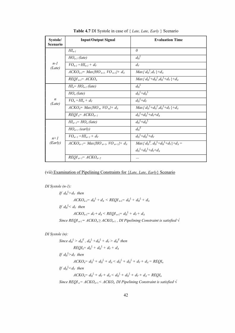
42
Table 4.7 DI Systole in case of { Late, Late, Early } Scenario
Systole/ Scenario
Input/Output Signal Evaluation Time
HIn-1 0
HOn-1 (late) dHL
VOn-1 =HIn-1 + dV dV
ACKOn-1= Max{HO n-1, VO n-1}+ dA Max{ dHL,dV }+dA
n-1 (Late)
REQI n-1= ACKOn Max{ dHL+dH
L,dHL+dV }+dA
HIn= HOn-1 (late) dHL
HOn (late) dHL+dH
L
VOn =HIn + dV dHL+dV
ACKOn= Max{HO n, VO n}+ dA Max{ dHL+dH
L,dHL+dV }+dA
n (Late)
REQI n= ACKOn+1 dHL+dH
L+dV+dA
HIn+1= HOn (late) dHL+dH
L
HOn+1 (early) dHE
VOn+1 =HIn+1 + dV dHL+dH
L+dV
ACKOn+1= Max{HO n+1, VO n+1}+ dA Max{ dHE, dH
L+dHL+dV}+dA =
dHL+dH
L+dV+dA
n+1 (Early)
REQI n+1= ACKOn+2 …
(vii) Examination of Pipelining Constraints for {Late, Late, Early} Scenario
DI Systole (n-1):
If dHL>dV then
ACKOn-1= dHL + dA < REQI n-1= dH
L + dHL + dA
If dHL< dV then
ACKOn-1= dV + dA < REQI n-1= dHL + dV + dA
Since REQI n-1 = ACKOn ≥ ACKOn-1 , DI Pipelining Constraint is satisfied √
DI Systole (n):
Since dHL > dH
E , dHL +dH
L + dV > dHE then
REQIn= dHL + dH
L + dV + dA
If dHL>dV then
ACKOn= dHL + dH
L + dA < dHL + dH
L + dV + dA = REQIn
If dHL<dV then
ACKOn= dHL + dV + dA < dH
L + dHL + dV + dA = REQIn
Since REQI n = ACKOn+1 < ACKOn DI Pipelining Constraint is satisfied √
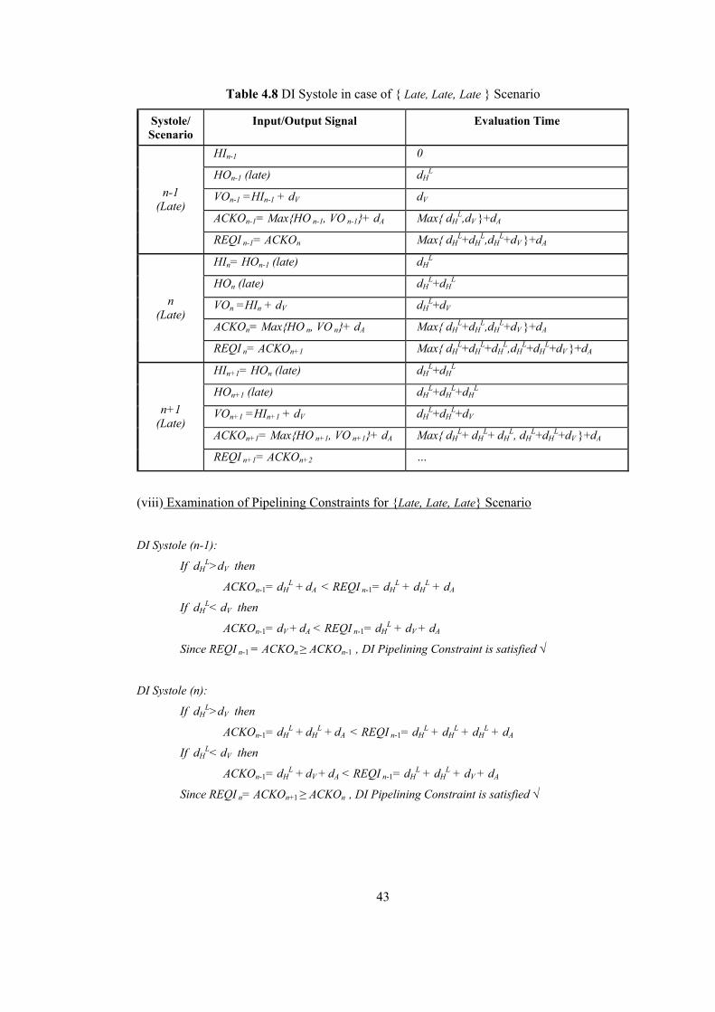
43
Table 4.8 DI Systole in case of { Late, Late, Late } Scenario
Systole/ Scenario
Input/Output Signal Evaluation Time
HIn-1 0
HOn-1 (late) dHL
VOn-1 =HIn-1 + dV dV
ACKOn-1= Max{HO n-1, VO n-1}+ dA Max{ dHL,dV }+dA
n-1 (Late)
REQI n-1= ACKOn Max{ dHL+dH
L,dHL+dV }+dA
HIn= HOn-1 (late) dHL
HOn (late) dHL+dH
L
VOn =HIn + dV dHL+dV
ACKOn= Max{HO n, VO n}+ dA Max{ dHL+dH
L,dHL+dV }+dA
n (Late)
REQI n= ACKOn+1 Max{ dHL+dH
L+dHL,dH
L+dHL+dV }+dA
HIn+1= HOn (late) dHL+dH
L
HOn+1 (late) dHL+dH
L+dHL
VOn+1 =HIn+1 + dV dHL+dH
L+dV
ACKOn+1= Max{HO n+1, VO n+1}+ dA Max{ dHL+ dH
L+ dHL, dH
L+dHL+dV }+dA
n+1 (Late)
REQI n+1= ACKOn+2 …
(viii) Examination of Pipelining Constraints for {Late, Late, Late} Scenario
DI Systole (n-1):
If dHL>dV then
ACKOn-1= dHL + dA < REQI n-1= dH
L + dHL + dA
If dHL< dV then
ACKOn-1= dV + dA < REQI n-1= dHL + dV + dA
Since REQI n-1 = ACKOn ≥ ACKOn-1 , DI Pipelining Constraint is satisfied √
DI Systole (n):
If dHL>dV then
ACKOn-1= dHL + dH
L + dA < REQI n-1= dHL + dH
L + dHL + dA
If dHL< dV then
ACKOn-1= dHL + dV + dA < REQI n-1= dH
L + dHL + dV + dA
Since REQI n= ACKOn+1 ≥ ACKOn , DI Pipelining Constraint is satisfied √
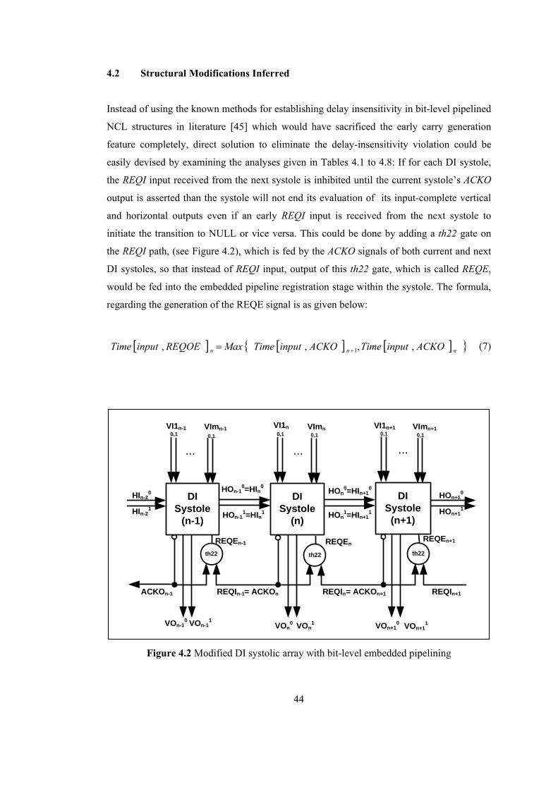
44
4.2 Structural Modifications Inferred
Instead of using the known methods for establishing delay insensitivity in bit-level pipelined
NCL structures in literature [45] which would have sacrificed the early carry generation
feature completely, direct solution to eliminate the delay-insensitivity violation could be
easily devised by examining the analyses given in Tables 4.1 to 4.8: If for each DI systole,
the REQI input received from the next systole is inhibited until the current systole’s ACKO
output is asserted than the systole will not end its evaluation of its input-complete vertical
and horizontal outputs even if an early REQI input is received from the next systole to
initiate the transition to NULL or vice versa. This could be done by adding a th22 gate on
the REQI path, (see Figure 4.2), which is fed by the ACKO signals of both current and next
DI systoles, so that instead of REQI input, output of this th22 gate, which is called REQE,
would be fed into the embedded pipeline registration stage within the systole. The formula,
regarding the generation of the REQE signal is as given below:
[ ] { [ ] [ ] }nnn ACKOinputTimeACKOinputTimeMaxREQOEinputTime ,,,, 1+= (7)
REQIn= ACKOn+1 REQIn+1REQIn-1= ACKOn
HIn-20
ACKOn-1
VI1n-10,1
VI1n0,1
...
VI1n+10,1
...
VImn-10,1
VImn0,1
VImn+10,1
HIn-21
...
HOn-10=HIn0
HOn+10
HOn+11
VOn-10 VOn-1
1VOn
0 VOn1 VOn+1
0 VOn+11
HOn-11=HIn1
HOn0=HIn+1
0
HOn1=HIn+1
1
DI Systole
(n+1)
th22 th22 th22
REQEn-1 REQEnREQEn+1
DI Systole
(n)
DI Systole
(n-1)
Figure 4.2 Modified DI systolic array with bit-level embedded pipelining
45
Then for the modified DI Systolic array, to satisfy the requirements of delay-insensitivity,
the evaluation time of the ACKO output of each systole should be smaller than or equal to
the evaluation time for the REQOE signal within the systole, which is generated from the
ACKO outputs of the current and next systoles. In other words, the DI Pipelining constraint
becomes:
[ ] [ ]nn REQOEinputTimeACKOinputTime ,, ≤ (8)
Re-application of the SDIVA method to modified DI Systolic Array is given in Tables 4.9 to
4.10 for delay-insensitivity violating input scenarios {Late, Early, Early} and {Late, Early,
Late}.
This solution resembles the “Broad Data Validity” scheme mentioned in [73] for bundled
data style asynchronous systems applied to dual-rail signals. The main difference is that the
modification is handled without introducing any extra control signals such as “validity”, i.e.
without complicating the inter-systole interfaces.
Meanwhile the early output evaluation capability of the modified DI systole is not hindered
with the addition of the new gate. The evaluation time of the Horizontal Output is only
slightly increased with the addition of the th22 gate on the REQI path. Besides, the speed up
advantages due to early output evaluation are still maintained as opposed to the completion-
completeness resolving methods proposed in [45]. For those input sets which do not require
arrival of the Horizontal Input from the previous systole to evaluate the Horizontal Output,
input-incomplete and early Horizontal Output evaluation still works as before, which could
also be easily verified by applying the analysis method for all the other scenarios [74].
Analysis of the fastest input scenario, {Early, Early, Early} is given in Table 4.11 as an
example.

46
Table 4.9 Modified DI Systole in case of { Late, Early, Early } Scenario
Systole/ Scenario
Input/Output Signal Evaluation Time
HIn-1 0
HOn-1 (late) dHL
VOn-1 =HIn-1 + dV dV
ACKOn-1= Max{HO n-1, VO n-1}+ dA Max{ dHL,dV}+dA
REQI n-1= ACKOn dHL+dV +dA
n-1 (Late)
REQE n-1=
Max{ ACKOn, ACKOn-1}+dB
Max{ dHL+dA, dV+dA, dH
L+dV +dA }+dB =
dHL+dV +dA+dB
HIn= HOn-1 (late) dHL
HOn (early) dHE
VOn =HIn + dV dHL+dV
ACKOn= Max{HO n, VO n}+ dA Max{ dHE,dH
L+dV }+dA = dHL+dV+dA
REQI n= ACKOn+1 dHE+dV+dA
n (Early)
REQE n=
Max{ ACKOn+1, ACKOn1}+dB
Max{ dHL+dV+dA, dH
E+dV+dA)}+dB =
dHL+dV+dA+dB
HIn+1= HOn (early) dHE
HOn+1 (early) dHE
VOn+1 =HIn+1 + dV dHE+dV
ACKOn+1= Max{HO n+1, VO n+1}+
dA
Max{ dHE,dH
E+dV }+dA = dHE+dV+dA
REQI n+1= ACKOn+2
n+1 (Early)
REQE n+1=
Max{ ACKOn+2, ACKOn+1}+dB
(i) Examination of Modified DICSA Systole for {Late, Early, Early} Scenario
Modified DICSA Systole (n):
Since dHL + dV > dH
E then
ACKOn= dHL + dV + dA
Since dHE + dV > dH
E then
REQI n= dHE + dV + dA
Since ACKOn=dHL + dV + dA > dH
E + dV + dA= REQI n then
REQE n= ACKOn+ dB = dHL + dV + dA + dB > dH
L + dV + dA =ACKOn
Since REQE n> ACKOn , DI Pipelining Constraint is satisfied √
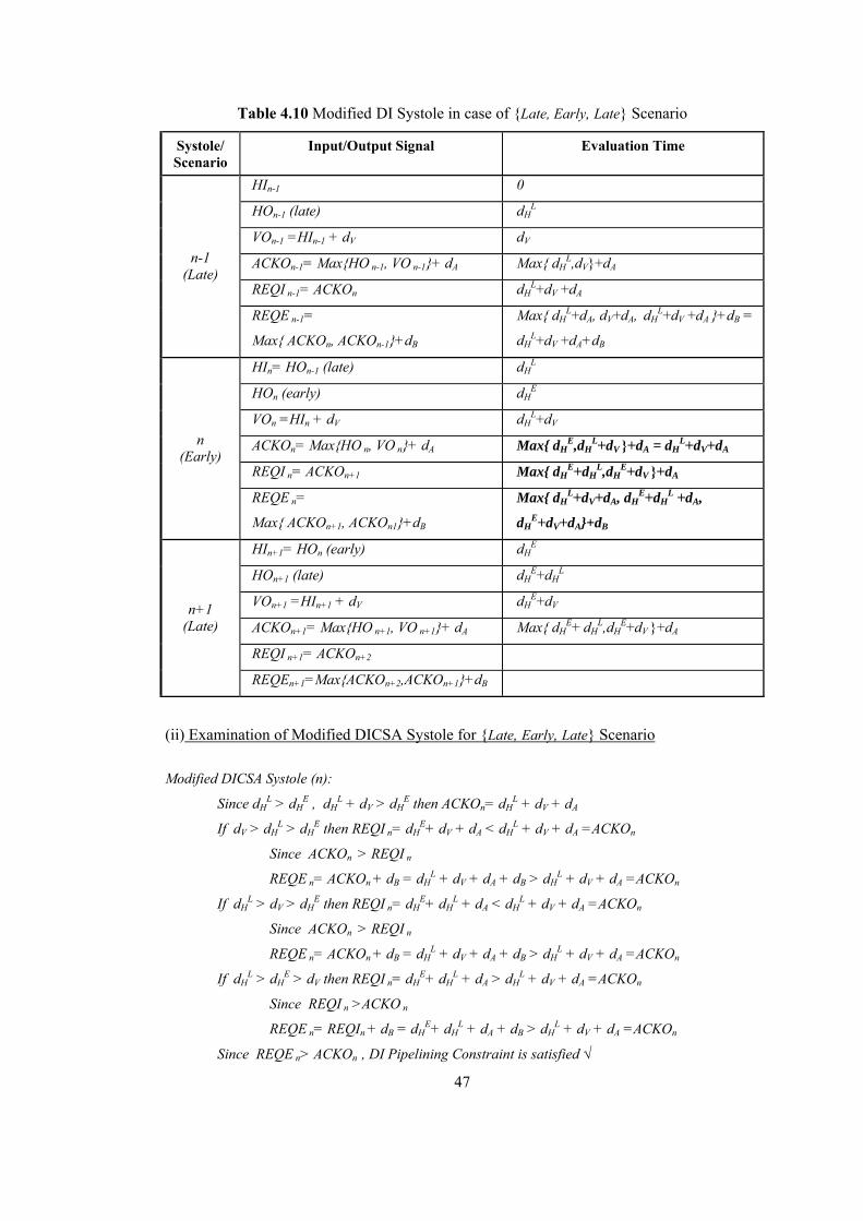
47
Table 4.10 Modified DI Systole in case of {Late, Early, Late} Scenario
Systole/ Scenario
Input/Output Signal Evaluation Time
HIn-1 0
HOn-1 (late) dHL
VOn-1 =HIn-1 + dV dV
ACKOn-1= Max{HO n-1, VO n-1}+ dA Max{ dHL,dV}+dA
REQI n-1= ACKOn dHL+dV +dA
n-1 (Late)
REQE n-1=
Max{ ACKOn, ACKOn-1}+dB
Max{ dHL+dA, dV+dA, dH
L+dV +dA }+dB =
dHL+dV +dA+dB
HIn= HOn-1 (late) dHL
HOn (early) dHE
VOn =HIn + dV dHL+dV
ACKOn= Max{HO n, VO n}+ dA Max{ dHE,dH
L+dV }+dA = dHL+dV+dA
REQI n= ACKOn+1 Max{ dHE+dH
L,dHE+dV }+dA
n (Early)
REQE n=
Max{ ACKOn+1, ACKOn1}+dB
Max{ dHL+dV+dA, dH
E+dHL +dA,
dHE+dV+dA}+dB
HIn+1= HOn (early) dHE
HOn+1 (late) dHE+dH
L
VOn+1 =HIn+1 + dV dHE+dV
ACKOn+1= Max{HO n+1, VO n+1}+ dA Max{ dHE+ dH
L,dHE+dV }+dA
REQI n+1= ACKOn+2
n+1 (Late)
REQEn+1=Max{ACKOn+2,ACKOn+1}+dB
(ii) Examination of Modified DICSA Systole for {Late, Early, Late} Scenario
Modified DICSA Systole (n):
Since dHL > dH
E , dHL + dV > dH
E then ACKOn= dHL + dV + dA
If dV > dHL > dH
E then REQI n= dHE+ dV + dA < dH
L + dV + dA =ACKOn
Since ACKOn > REQI n
REQE n= ACKOn + dB = dHL + dV + dA + dB > dH
L + dV + dA =ACKOn
If dHL > dV > dH
E then REQI n= dHE+ dH
L + dA < dHL + dV + dA =ACKOn
Since ACKOn > REQI n
REQE n= ACKOn + dB = dHL + dV + dA + dB > dH
L + dV + dA =ACKOn
If dHL > dH
E > dV then REQI n= dHE+ dH
L + dA > dHL + dV + dA =ACKOn
Since REQI n >ACKO n
REQE n= REQIn + dB = dHE+ dH
L + dA + dB > dHL + dV + dA =ACKOn
Since REQE n> ACKOn , DI Pipelining Constraint is satisfied √
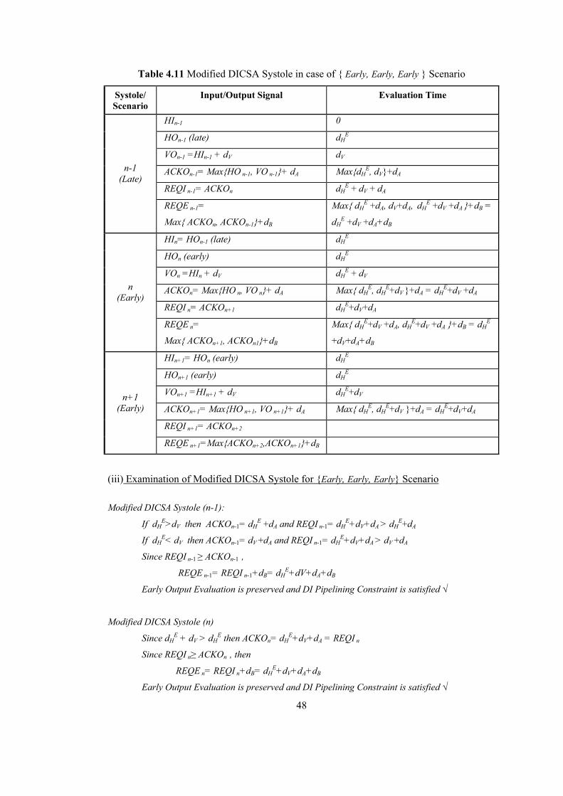
48
Table 4.11 Modified DICSA Systole in case of { Early, Early, Early } Scenario
Systole/ Scenario
Input/Output Signal Evaluation Time
HIn-1 0
HOn-1 (late) dHE
VOn-1 =HIn-1 + dV dV
ACKOn-1= Max{HO n-1, VO n-1}+ dA Max{dHE, dV}+dA
REQI n-1= ACKOn dHE + dV + dA
n-1 (Late)
REQE n-1=
Max{ ACKOn, ACKOn-1}+dB
Max{ dHE +dA, dV+dA, dH
E +dV +dA }+dB =
dHE +dV +dA+dB
HIn= HOn-1 (late) dHE
HOn (early) dHE
VOn =HIn + dV dHE + dV
ACKOn= Max{HO n, VO n}+ dA Max{ dHE, dH
E+dV }+dA = dHE+dV +dA
REQI n= ACKOn+1 dHE+dV+dA
n (Early)
REQE n=
Max{ ACKOn+1, ACKOn1}+dB
Max{ dHE+dV +dA, dH
E+dV +dA }+dB = dHE
+dV+dA+dB
HIn+1= HOn (early) dHE
HOn+1 (early) dHE
VOn+1 =HIn+1 + dV dHE+dV
ACKOn+1= Max{HO n+1, VO n+1}+ dA Max{ dHE, dH
E+dV }+dA = dHE+dV+dA
REQI n+1= ACKOn+2
n+1 (Early)
REQE n+1=Max{ACKOn+2,ACKOn+1}+dB
(iii) Examination of Modified DICSA Systole for {Early, Early, Early} Scenario
Modified DICSA Systole (n-1):
If dHE>dV then ACKOn-1= dH
E +dA and REQI n-1= dHE+dV+dA > dH
E+dA
If dHE< dV then ACKOn-1= dV +dA and REQI n-1= dH
E+dV+dA > dV +dA
Since REQI n-1 ≥ ACKOn-1 ,
REQE n-1= REQI n-1+dB= dHE+dV+dA+dB
Early Output Evaluation is preserved and DI Pipelining Constraint is satisfied √
Modified DICSA Systole (n)
Since dHE + dV > dH
E then ACKOn= dHE+dV+dA = REQI n
Since REQI n≥ ACKOn , then
REQE n= REQI n+dB= dHE+dV+dA+dB
Early Output Evaluation is preserved and DI Pipelining Constraint is satisfied √
49
4.3 Benefits of the SDIVA Method
The SDIVA method employs symbolic delays for all output paths and analyses the signal
flow on three adjacent systoles for all possible early/late carry generation conditions, to
detect and correct the cases of early generation or no generation of completion
acknowledgment. The verification of a complete systolic adder is reduced to verification of
three systoles, regardless of the operand length of the adder, which is a significant saving in
verification effort and time, especially when compared to formal analysis methods which are
usually based on exploration of all reachable states hence suffer from the state explosion
problem.
Application of the SDIVA method to a typical delay-insensitive bit-level pipelined systolic
array in dual-line threshold logic style with early output evaluation possibilities in one-
dimension demonstrated that, the analyses could further be simplified down to examination
of two offending input scenarios, namely {Late, Early, Early} and {Late, Early, Late} and
with this method, it is also possible to easily devise structural modifications to offending
topologies without sacrificing the early output evaluation features and the resultant speed up
advantages.
Although the presented work concentrates on a particular class of bit-level pipelined systolic
array, the SDIVA method is generic enough in that:
• It is independent of operand length since evaluation of three adjacent systoles is
sufficient;
• It does not require actual path/gate delays but only symbolic ones to represent
relative lengths of early/late output generation paths.
• It not only analysis delay insensitivity but also evaluates the speed-up issues
inherent in the topology.
• It is completely technology independent, so verification is robust against all physical
and environmental parameters
• It could be safely applied to other systolic arrays having more than one early output
evaluation paths in one dimension or multiple early output evaluation paths in more
than one dimension.
50
CHAPTER 5
5 DELAY INSENSITIVE SYSTOLIC ADDER DESIGN Binary addition resides at the critical path of most signal processing systems, so improving
the critical path of addition is usually the key to improving the overall throughput of a data
processing circuit. The complexity of binary addition is directly related to its operand length.
When the operand size of the adder is large, either long carry propagation delays are
suffered to keep the silicon area low, -as in the case of ripple-carry adders-, or other adder
topologies are introduced to improve speed at the expense of silicon area, as in the case of
carry look-ahead adders. Pipelining and systolic array structures also help to divide the
critical path and the increase overall throughput of addition-based data processing circuits.
Ripple carry style adders which could be easily converted into small identical and repeatable
units (systoles) and which propagate the carry output of addition along row full adder
systoles as carry input to the next systolic adder benefit the most form pipelining. But, even
if pipelined at bit-level, the performance of synchronous systolic array adders is always
bounded by the worst case of the critical path , i.e. the longest carry propagation path which
is equal to the operand size of the adder. Bit-level pipelining may divide the n-bit carry
propagation path into 1-bit full adder carry evaluation paths but the n-bit addition still
requires n clock cycles to complete.
In [65], it is claimed that, in the average, carry propagation steps of n-bit binary addition
converge to log2n and n-bit carry propagation is extremely rare. But since synchronous
circuits are designed to handle the worst case, they are designed for handling n-bit carry
propagation. For example, for the 1024-Bit RSA crypto-processor IC [66], utilizing
synchronous systolic array architecture to perform a highly compute-intensive
exponentiation operation, namely the Montgomery Modular Multiplication algorithm [67],
the critical path of the design is the 1024-bit carry propagation path. An extensive statistical
analysis carried out on this IC by means of a RSA encryption/decryption simulator program,
which records all partial product terms formed during RSA encryption sessions and the
lengths of all carry propagations in the addition operations performed at each step of
Montgomery Modular Multiplication, confirm the above stated facts: In all the 1024-bit
additions performed during RSA encryption sessions, where the addition operands display a
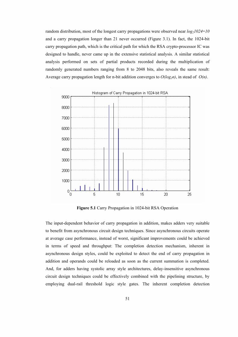
51
random distribution, most of the longest carry propagations were observed near log21024=10
and a carry propagation longer than 21 never occurred (Figure 3.1). In fact, the 1024-bit
carry propagation path, which is the critical path for which the RSA crypto-processor IC was
designed to handle, never came up in the extensive statistical analysis. A similar statistical
analysis performed on sets of partial products recorded during the multiplication of
randomly generated numbers ranging from 8 to 2048 bits, also reveals the same result:
Average carry propagation length for n-bit addition converges to O(log2n), in stead of O(n).
Figure 5.1 Carry Propagation in 1024-bit RSA Operation
The input-dependent behavior of carry propagation in addition, makes adders very suitable
to benefit from asynchronous circuit design techniques. Since asynchronous circuits operate
at average case performance, instead of worst, significant improvements could be achieved
in terms of speed and throughput: The completion detection mechanism, inherent in
asynchronous design styles, could be exploited to detect the end of carry propagation in
addition and operands could be reloaded as soon as the current summation is completed.
And, for adders having systolic array style architectures, delay-insensitive asynchronous
circuit design techniques could be effectively combined with the pipelining structure, by
employing dual-rail threshold logic style gates. The inherent completion detection
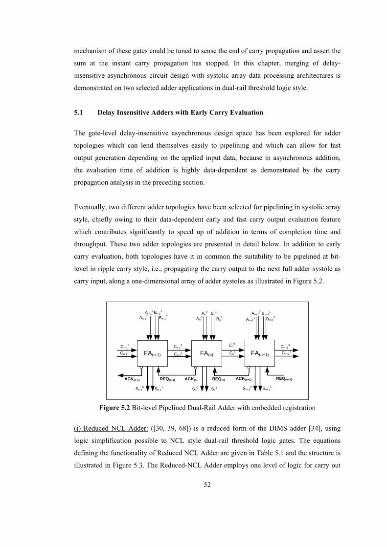
52
mechanism of these gates could be tuned to sense the end of carry propagation and assert the
sum at the instant carry propagation has stopped. In this chapter, merging of delay-
insensitive asynchronous circuit design with systolic array data processing architectures is
demonstrated on two selected adder applications in dual-rail threshold logic style.
5.1 Delay Insensitive Adders with Early Carry Evaluation
The gate-level delay-insensitive asynchronous design space has been explored for adder
topologies which can lend themselves easily to pipelining and which can allow for fast
output generation depending on the applied input data, because in asynchronous addition,
the evaluation time of addition is highly data-dependent as demonstrated by the carry
propagation analysis in the preceding section.
Eventually, two different adder topologies have been selected for pipelining in systolic array
style, chiefly owing to their data-dependent early and fast carry output evaluation feature
which contributes significantly to speed up of addition in terms of completion time and
throughput. These two adder topologies are presented in detail below. In addition to early
carry evaluation, both topologies have it in common the suitability to be pipelined at bit-
level in ripple carry style, i.e., propagating the carry output to the next full adder systole as
carry input, along a one-dimensional array of adder systoles as illustrated in Figure 5.2.
FA(n-1)
REQ(n) ACK(n+1)
FA(n)
REQ(n+1)
Sn-10 Sn-1
1
REQ(n-1) ACK(n)
Sn0 Sn
1
An-10 Bn-1
1
An-11 Bn-1
0An
0 Bn1
An1 Bn
0
Cn-10
Cn-11
Cn0
Cn1 FA(n+1)
ACK(n-1)
Sn+10 Sn+1
1
Cn+10
Cn+11
An+10 Bn+1
1
An+11 Bn+1
0
Cn-10
Cn-11
Figure 5.2 Bit-level Pipelined Dual-Rail Adder with embedded registration
(i) Reduced NCL Adder: ([30, 39, 68]) is a reduced form of the DIMS adder [34], using
logic simplification possible to NCL style dual-rail threshold logic gates. The equations
defining the functionality of Reduced NCL Adder are given in Table 5.1 and the structure is
illustrated in Figure 5.3. The Reduced-NCL Adder employs one level of logic for carry out
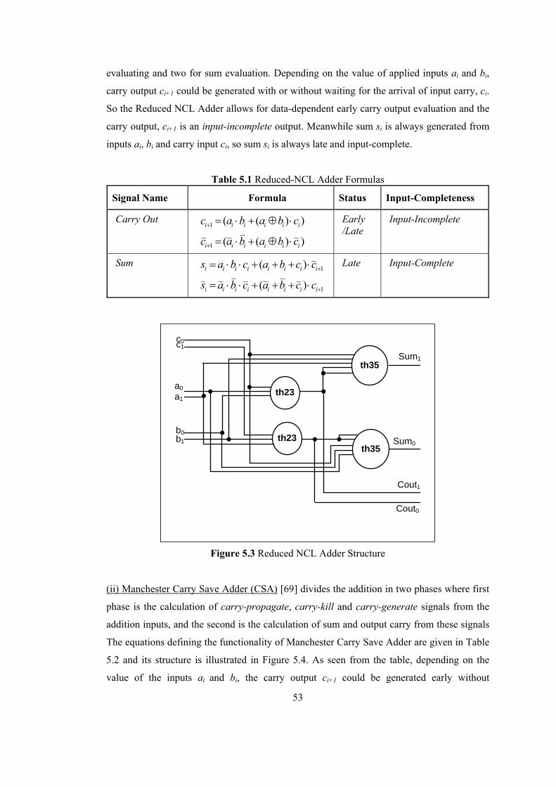
53
evaluating and two for sum evaluation. Depending on the value of applied inputs ai and bi,
carry output ci+1 could be generated with or without waiting for the arrival of input carry, ci.
So the Reduced NCL Adder allows for data-dependent early carry output evaluation and the
carry output, ci+1 is an input-incomplete output. Meanwhile sum si is always generated from
inputs ai, bi and carry input ci, so sum si is always late and input-complete.
Table 5.1 Reduced-NCL Adder Formulas
Signal Name Formula Status Input-Completeness
Carry Out ))((1 iiiiii cbabac ⋅⊕+⋅=+
))((1 iiiiii cbabac ⋅⊕+⋅=+
Early /Late
Input-Incomplete
Sum 1)( +⋅+++⋅⋅= iiiiiiii ccbacbas
1)( +⋅+++⋅⋅= iiiiiiii ccbacbas
Late Input-Complete
c1c0
Cout1
Cout0
Sum1
th23
th23
a1
a0
b1
b0
th35
th35Sum0
Figure 5.3 Reduced NCL Adder Structure
(ii) Manchester Carry Save Adder (CSA) [69] divides the addition in two phases where first
phase is the calculation of carry-propagate, carry-kill and carry-generate signals from the
addition inputs, and the second is the calculation of sum and output carry from these signals
The equations defining the functionality of Manchester Carry Save Adder are given in Table
5.2 and its structure is illustrated in Figure 5.4. As seen from the table, depending on the
value of the inputs ai and bi, the carry output ci+1 could be generated early without
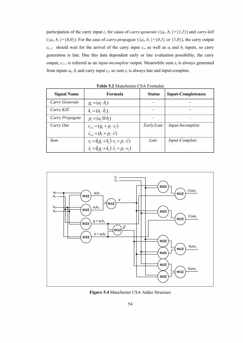
54
participation of the carry input ci for cases of carry-generate ({ai, bi }={1,1}) and carry-kill
({ai, bi }={0,0}). For the case of carry-propagate ({ai, bi }={0,1} or {1,0}), the carry output
ci+1 should wait for the arrival of the carry input ci, as well as ai and bi inputs, so carry
generation is late. Due this data dependent early or late evaluation possibility, the carry
output, ci+1 is referred as an input-incomplete output. Meanwhile sum si is always generated
from inputs ai, bi and carry input ci, so sum si is always late and input-complete.
Table 5.2 Manchester CSA Formulas
Signal Name Formula Status Input-Completeness
Carry Generate )( iii bag ⋅= - -
Carry Kill iiii bak )( ⋅= - -
Carry Propagate )( iii bap ⊕= - -
Carry Out )(1 iiii cpgc ⋅+=+
)(1 cpkc iii ⋅+=+
Early/Late Input-Incomplete
Sum ( ) )( cpckgs iiiii ⋅+⋅+= ( ) )( iiiiii cpckgs ⋅+⋅+=
Late Input-Complete
a0b1
a1b0
g = a1b1
k = a0b0
th22
th22
th22
th22
a1
a0
b1
b0
c1c0
Cout1
Cout0
Sum1
Sum0
p
p
th22
th12
th22
th12
th22
th22
th22
th22
th12
th12
th12
th12
Figure 5.4 Manchester CSA Adder Structure
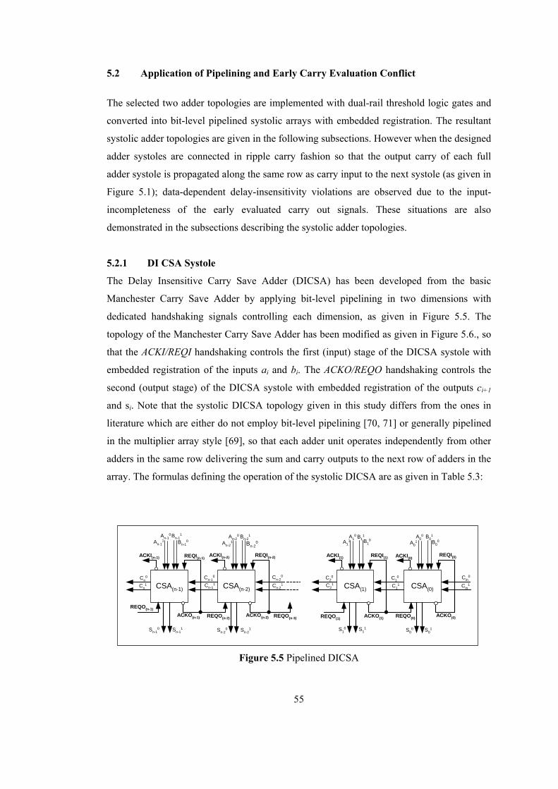
55
5.2 Application of Pipelining and Early Carry Evaluation Conflict
The selected two adder topologies are implemented with dual-rail threshold logic gates and
converted into bit-level pipelined systolic arrays with embedded registration. The resultant
systolic adder topologies are given in the following subsections. However when the designed
adder systoles are connected in ripple carry fashion so that the output carry of each full
adder systole is propagated along the same row as carry input to the next systole (as given in
Figure 5.1); data-dependent delay-insensitivity violations are observed due to the input-
incompleteness of the early evaluated carry out signals. These situations are also
demonstrated in the subsections describing the systolic adder topologies.
5.2.1 DI CSA Systole
The Delay Insensitive Carry Save Adder (DICSA) has been developed from the basic
Manchester Carry Save Adder by applying bit-level pipelining in two dimensions with
dedicated handshaking signals controlling each dimension, as given in Figure 5.5. The
topology of the Manchester Carry Save Adder has been modified as given in Figure 5.6., so
that the ACKI/REQI handshaking controls the first (input) stage of the DICSA systole with
embedded registration of the inputs ai and bi. The ACKO/REQO handshaking controls the
second (output stage) of the DICSA systole with embedded registration of the outputs ci+1
and si. Note that the systolic DICSA topology given in this study differs from the ones in
literature which are either do not employ bit-level pipelining [70, 71] or generally pipelined
in the multiplier array style [69], so that each adder unit operates independently from other
adders in the same row delivering the sum and carry outputs to the next row of adders in the
array. The formulas defining the operation of the systolic DICSA are as given in Table 5.3:
CSA(n-1)
REQO(n-2)ACKO(n-1)
CSA(n-2)
REQO(n-1)
Sn-10 Sn-1
1
REQO(n-3)ACKO(n-2)
Sn-20 Sn-2
1
An-10Bn-1
1
An-11 Bn-1
0
ACKI(n-1) REQI(n-1)
An-20 Bn-2
1
An-21 Bn-2
0
ACKI(n-2) REQI(n-2)
Cn0
Cn1
Cn-10
Cn-11
Cn-20
Cn-21 CSA(1)
REQO(0)ACKO(1)
CSA(0)
REQO(1)
S10 S1
1
ACKO(0)
S00 S0
1
C10
C11
A10 B1
1
A11 B1
0
ACKI(1) REQI(1)
A00 B0
1
A01 B0
0
ACKI(0)REQI(0)
C20
C21
Cin0
Cin1
Figure 5.5 Pipelined DICSA
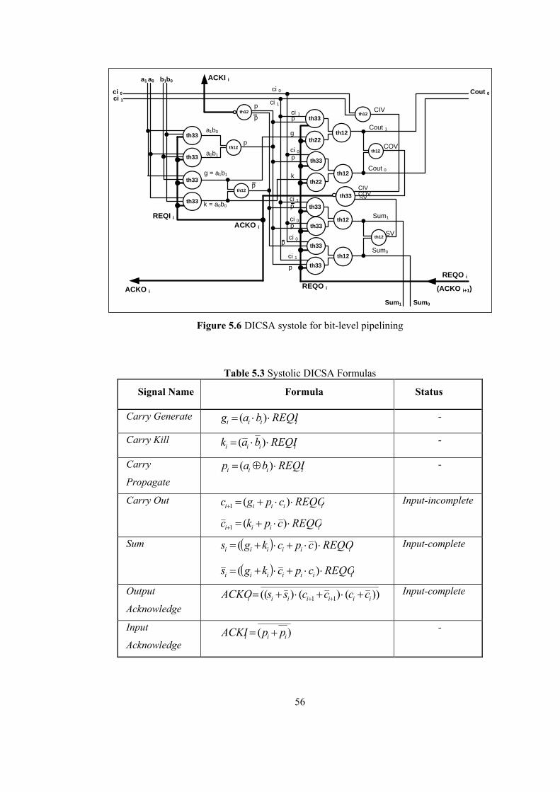
56
Cout 1
a0b1
a1b0
g = a1b1
k = a0b0
a1 a0 b1b0
ci 0
ci 1
Cout 1
Cout 0
Sum1
Sum0
p
th12
th12
th12
th12
(ACKO i+1)REQO i
ACKO iREQI i
ACKI i
p
p
p
p
pk
g
ci 1
ci 0
ci 0
ci 0
ci 1
ci 1
CIV
COV
SV
CIVCOVSV
p
ci 0ci 1
ACKO i
Cout 0
REQO i
Sum1 Sum0
p
p
p
th12
th12th12
th12
th12
th33
th33
th33
th33
th33
th22th12
th33
th33
th22
th33
th33
th33
th33
Figure 5.6 DICSA systole for bit-level pipelining
Table 5.3 Systolic DICSA Formulas
Signal Name Formula Status
Carry Generate iiii REQIbag ⋅⋅= )( -
Carry Kill iiii REQIbak ⋅⋅= )( -
Carry
Propagate iiii REQIbap ⋅⊕= )( -
Carry Out iiiii REQOcpgc ⋅⋅+=+ )(1
iiii REQOcpkc ⋅⋅+=+ )(1
Input-incomplete
Sum ( ) iiiiii REQOcpckgs ⋅⋅+⋅+= )(
( ) iiiiiii REQOcpckgs ⋅⋅+⋅+= )(
Input-complete
Output
Acknowledge ))()()(( 11 iiiiiii ccccssACKO +⋅+⋅+= ++ Input-complete
Input
Acknowledge )( iii ppACKI +=
-
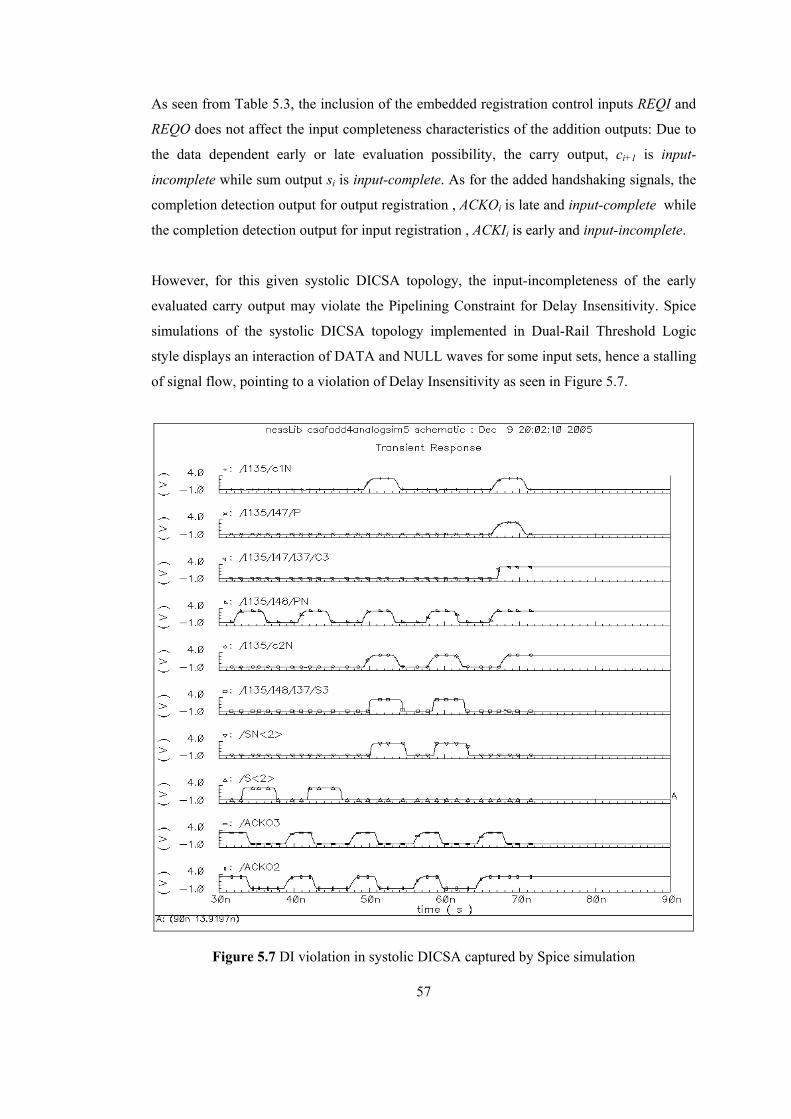
57
As seen from Table 5.3, the inclusion of the embedded registration control inputs REQI and
REQO does not affect the input completeness characteristics of the addition outputs: Due to
the data dependent early or late evaluation possibility, the carry output, ci+1 is input-
incomplete while sum output si is input-complete. As for the added handshaking signals, the
completion detection output for output registration , ACKOi is late and input-complete while
the completion detection output for input registration , ACKIi is early and input-incomplete.
However, for this given systolic DICSA topology, the input-incompleteness of the early
evaluated carry output may violate the Pipelining Constraint for Delay Insensitivity. Spice
simulations of the systolic DICSA topology implemented in Dual-Rail Threshold Logic
style displays an interaction of DATA and NULL waves for some input sets, hence a stalling
of signal flow, pointing to a violation of Delay Insensitivity as seen in Figure 5.7.
Figure 5.7 DI violation in systolic DICSA captured by Spice simulation
58
The SDIVA method proposed in Chapter 4 is applied to the systolic DICSA array of 3
systoles, by assigning the below given symbolic delays to the output paths:
dCE delay of carry output path in case of early evaluation (input-incomplete)
dCL delay of carry output path in case of late evaluation (input-complete)
dS delay of the sum output path (input-complete)
dA delay of the completion detection path, ACKO, (input-complete)
And the analysis started with the following assumptions:
• Inputs ai and bi to all systoles and the carry input to the leftmost systole, ci-1 are
applied concurrently
• All wire forks within the systoles are isochronic
• Since dCE and dC
L denote the delays of the same path, in cases of input-
incomplete/early and input-complete/late carry evaluation respectively, the delay, dCE is
always smaller than the delay dCL:
L
CE
C dd < (9)
Without making any other assumptions about the relative magnitudes of the output delays
and leaving the handshaking signals of the input registration stage, ACKI/REQI out of the
analysis, -since they do not have any affect on the output delays-, the evaluation time of
ACKO output from the time of inputs’ application is calculated in terms of the symbolic
delays, dS, dA, dCE, dC
L for all of the 8 possible input scenarios and checked against the
pipelining constraint, which becomes as given in (10), for the systolic DICSA array:
[ ] [ ] [ ]nnn REQOinputTimeACKOinputTimeACKOinputTime ,,, 1 =≥ + (10)
Application of the SDIVA method reveals that for the input scenarios {Late, Early, Early}
and {Late, Early, Late}, delay-insensitivity is violated as indicated by the bold lettering in
Table 5.4 and Table 5.5. For these two scenarios, it is clearly seen that the evaluation time
for the ACKO output of (n+1)th systole, which is also the REQO input arrival time for nth
systole, is smaller than the evaluation time for ACKO output of the nth systole. So NULL and
DATA wavefronts would interact within nth systole and violate delay-insensitivity. The
result is no generation of the ACK output of nth systole and consecutively blocking of signal
flow.
59
In these tables, the following abbreviations are used:
CI : Carry Input,
CO: : Carry Output,
SO : Sum Output
REQO : REQ Input to the output stage,
ACKO : ACK Output of the output stage
Table 5.4 DICSA Systole in case of {Late, Early, Early} Scenario
Systole/ Scenario
Input/Output Signal Evaluation Time
CIn-1 0
COn-1(late) dCL
SOn-1= CIn-1 + dS dS
ACKOn-1= Max{SOn-1, COn-1}+ dA Max {dCL,dS}+dA
n-1 (Late)
REQOn-1= ACKOn dCL+dS+dA
CIn= COn-1 (late) dCL
COn(early) dCE
SOn = CIn + dS dCL+ dS
ACKOn= Max{SOn, COn}+ dA Max{dCE, dC
L+dS}+dA=dCL+dS+dA
n (Early)
REQOn= ACKOn+1 dCE+dS+dA
CIn+1= COn(early) dCE
COn+1(early) dCE
SOn+1= CIn+1 + dS dCE+dS
ACKOn+1= Max{SOn+1, COn+1}+ dA Max{ dCE,dC
E+dS }+dA = dCE+dS+dA
n+1 (Early)
REQOn+1= ACKOn+2 …
Examination of DICSA Systole (n-1):
If dCL>dS then ACKOn-1= dC
L + dA and REQO n-1= dCL + dS + dA > dC
L +dA
If dHL< dV then ACKOn-1= dS + dA and REQO n-1= dC
L + dS + dA > dS +dA
Since REQO n-1 = ACKOn ≥ ACKOn-1 , DI Pipelining Constraint is satisfied √
Examination of DICSA Systole (n):
Since dCL> dC
E, dCL + dS > dC
E then ACKOn= dCL + dS + dA
Since dCL> dC
E, dCE + dS > dC
E then
REQO n= dCE + dS + dA < dC
L + dS + dA =ACKOn
Since REQOn = ACKOn+1 < ACKOn , DI Pipelining Constraint is violated !
60
Table 5.5 DICSA Systole in case of {Late, Early, Late} Scenario
Systole/ Scenario
Input/Output Signal Evaluation Time
CIn-1 0
COn-1(late) dCL
SOn-1= CIn-1 + dS dS
ACKOn-1= Max{SOn-1, COn-1}+ dA Max {dCL,dS}+dA
n-1 (Late)
REQOIn-1= ACKOn dCL+dS.+dA
CIn= COn-1 (late) dCL
COn(early) dCE
SOn= CIn + dS dCL+ dS
ACKOn= Max{SOn, COn}+ dA Max{dCE, dC
L+dS}+dA=dCL+dS+dA
n (Early)
REQOn= ACKOn+1 Max{ dCE+dC
L,dCE+dS }+dA
CIn+1= COn(early) dCE
COn+1(late) dCE+dC
L
SOn+1= CIn+1 + dS dCE+dS
ACKOn+1= Max{SOn+1, COn+1}+ dA Max{ dCE+ dC
L,dCE+dS }+dA
n+1 (Late)
REQOn+1= ACKOn+2 …
Examination of DICSA Systole (n-1):
If dCL>dS then
ACKOn-1= dCL + dA and REQO n-1= dC
L + dS + dA > dCL +dA
If dHL< dV then
ACKOn-1= dS + dA and REQO n-1= dCL + dS + dA > dS +dA
Since REQO n-1 = ACKOn ≥ ACKOn-1 , DI Pipelining Constraint is satisfied √
Examination of DICSA Systole (n):
Since dCL > dC
E, dCL + dS > dC
E then ACKOn= dCL + dS + dA
If dS > dCL > dC
E then
REQO n= dCE + dS + dA < dC
L + dS + dA =ACKOn
If dCL > dS > dC
E then
REQO n= dCE + dC
L + dA < dCL + dS+ dA =ACKOn
If dCL > dC
E > dS then
REQO n= dCE + dC
L + dA >dCL + dS+ dA =ACKOn
Since REQOn = ACKOn+1 < ACKOn ,in case dS > dCL or dC
L > dS > dCE
DI Pipelining Constraint is violated !
61
5.2.2 NCL Adder Systole
The NCL Adder systole has been developed from the reduced-NCL Adder [39], by applying
bit-level pipelining in one-dimension, so that the handshaking signals ACK/REQ control the
carry propagation flow as given in Figure 5.8. The topology of the reduced-NCL Adder has
been modified so that the REQ input is embedded in to the first stage of addition which
generates the carry output ci+1. Since the second stage of addition uses the output of the first
stage to generate the sum output si, REQ input also controls the sum output flow implicitly.
The formulas defining the operation of the NCL Adder systole are given in Table 5.6.
Figure 5.8 Pipelined Reduced-NCL Adder
c1c0
Cout1
Cout0
Sum1
th34
th34
a1
a0
b1
b0
th34w2 Sum0
b0
b1
a0c0
a0b0
c0Cout0
Cout1a1
b1
c1
a1
c1
Cout0
Cout1
(ACK i+1)REQ i REQ i
th12SV
th12COV
ACK i
th22
th34w2
Figure 5.9 The Reduced-NCL Adder systole
62
Table 5.6 Systolic Reduced-NCL Adder Formulas
Signal Name Formula Status
Carry Out iiiiiii REQcbabac ⋅⋅⊕+⋅=+ ))((1
iiiiiii REQcbabac ⋅⋅⊕+⋅=+ ))((1
Input-incomplete
Sum 1)( +⋅+++⋅⋅= iiiiiiii ccbacbas
1)( +⋅+++⋅⋅= iiiiiiii ccbacbas
Input-complete
Acknowledge ))()(( 11 ++ +⋅+= iiiii ccssACK Input-complete
As seen from Table 5.6, the inclusion of the embedded registration control input REQ does
not affect the input completeness characteristics of the addition outputs: Due to the data
dependent early or late evaluation possibility, the carry output, ci+1 is input-incomplete while
sum output si is input-complete. Also the added completion detection output for output
registration, ACKi is late and input-complete .
However, the Systolic NCL Adder topology also violates the Pipelining Constraint for Delay
Insensitivity for some inputs, due to the input-incompleteness of the early evaluated carry
output. Spice simulations of the Systolic NCL Adder topology implemented in Dual-Rail
Threshold Logic style displays an interaction of DATA and NULL waves in the same way
as the Systolic DICSA. For some input sets, signal flow is stalled, indicating a violation of
Delay Insensitivity. Applying the proposed Delay Insensitivity verification analysis method
to a Systolic NCL Adder array of 3 systoles reveals the input scenarios which violate Delay
Insensitivity. Assigning similar symbolic delays to the output paths and using the same
assumptions as the Systolic DICSA, the pipelining constraint given in () could be checked
for all of the 8 possible input scenarios that generate possible combinations of the Late/Early
Carry evaluation on three systoles. As given in Table 5.7, the Systolic NCL Adder exhibits
interaction of DATA and NULL waves for {Late, Early, Early} input scenario only. For this
scenario, it is clearly seen that the evaluation time for the ACK output of (n+1)th systole,
which is also the REQI input arrival time for nth systole, is smaller than the evaluation time
for ACKI output of the nth systole. So NULL and DATA wavefronts would interact within
nth systole and violate delay-insensitivity resulting in no generation of the ACK output of nth
systole and consecutively blocking of signal flow.
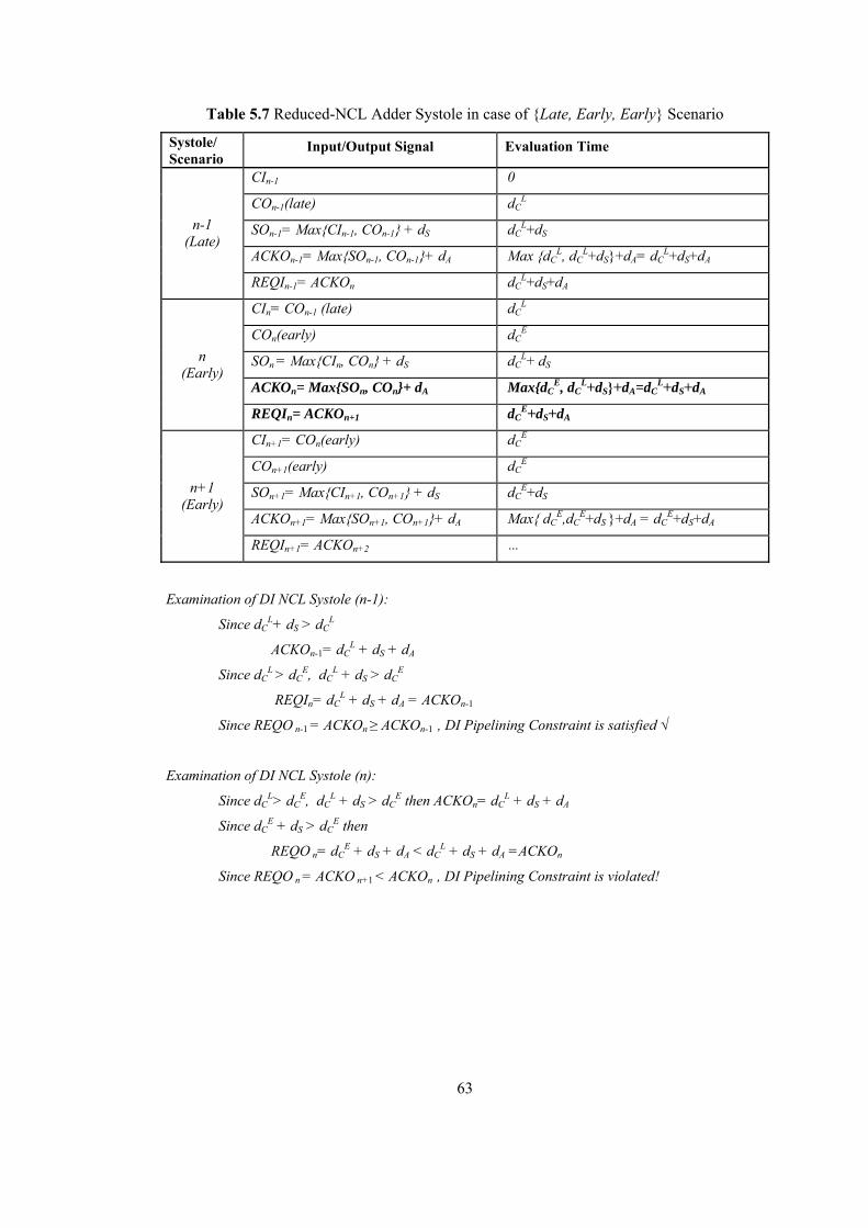
63
Table 5.7 Reduced-NCL Adder Systole in case of {Late, Early, Early} Scenario
Systole/ Scenario
Input/Output Signal Evaluation Time
CIn-1 0
COn-1(late) dCL
SOn-1= Max{CIn-1, COn-1} + dS dCL+dS
ACKOn-1= Max{SOn-1, COn-1}+ dA Max {dCL, dC
L+dS}+dA= dCL+dS+dA
n-1 (Late)
REQIn-1= ACKOn dCL+dS+dA
CIn= COn-1 (late) dCL
COn(early) dCE
SOn = Max{CIn, COn} + dS dCL+ dS
ACKOn= Max{SOn, COn}+ dA Max{dCE, dC
L+dS}+dA=dCL+dS+dA
n (Early)
REQIn= ACKOn+1 dCE+dS+dA
CIn+1= COn(early) dCE
COn+1(early) dCE
SOn+1= Max{CIn+1, COn+1} + dS dCE+dS
ACKOn+1= Max{SOn+1, COn+1}+ dA Max{ dCE,dC
E+dS }+dA = dCE+dS+dA
n+1 (Early)
REQIn+1= ACKOn+2 …
Examination of DI NCL Systole (n-1):
Since dCL+ dS > dC
L
ACKOn-1= dCL + dS + dA
Since dCL > dC
E, dCL + dS > dC
E
REQIn= dCL + dS + dA = ACKOn-1
Since REQO n-1 = ACKOn ≥ ACKOn-1 , DI Pipelining Constraint is satisfied √
Examination of DI NCL Systole (n):
Since dCL> dC
E, dCL + dS > dC
E then ACKOn= dCL + dS + dA
Since dCE + dS > dC
E then
REQO n= dCE + dS + dA < dC
L + dS + dA =ACKOn
Since REQO n = ACKO n+1 < ACKOn , DI Pipelining Constraint is violated!
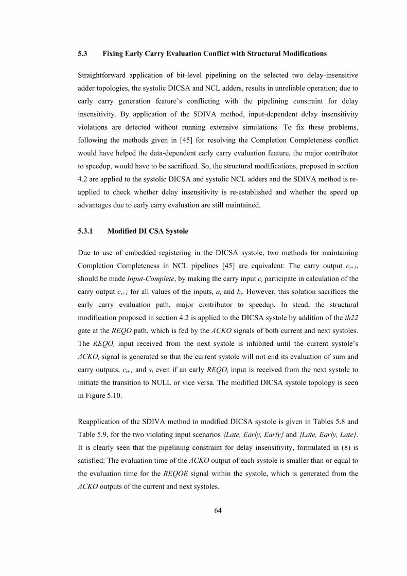
64
5.3 Fixing Early Carry Evaluation Conflict with Structural Modifications
Straightforward application of bit-level pipelining on the selected two delay-insensitive
adder topologies, the systolic DICSA and NCL adders, results in unreliable operation; due to
early carry generation feature’s conflicting with the pipelining constraint for delay
insensitivity. By application of the SDIVA method, input-dependent delay insensitivity
violations are detected without running extensive simulations. To fix these problems,
following the methods given in [45] for resolving the Completion Completeness conflict
would have helped the data-dependent early carry evaluation feature, the major contributor
to speedup, would have to be sacrificed. So, the structural modifications, proposed in section
4.2 are applied to the systolic DICSA and systolic NCL adders and the SDIVA method is re-
applied to check whether delay insensitivity is re-established and whether the speed up
advantages due to early carry evaluation are still maintained.
5.3.1 Modified DI CSA Systole
Due to use of embedded registering in the DICSA systole, two methods for maintaining
Completion Completeness in NCL pipelines [45] are equivalent: The carry output ci+1,
should be made Input-Complete, by making the carry input ci participate in calculation of the
carry output ci+1 for all values of the inputs, ai and bi. However, this solution sacrifices the
early carry evaluation path, major contributor to speedup. In stead, the structural
modification proposed in section 4.2 is applied to the DICSA systole by addition of the th22
gate at the REQO path, which is fed by the ACKO signals of both current and next systoles.
The REQOi input received from the next systole is inhibited until the current systole’s
ACKOi signal is generated so that the current systole will not end its evaluation of sum and
carry outputs, ci+1 and si even if an early REQOi input is received from the next systole to
initiate the transition to NULL or vice versa. The modified DICSA systole topology is seen
in Figure 5.10.
Reapplication of the SDIVA method to modified DICSA systole is given in Tables 5.8 and
Table 5.9, for the two violating input scenarios {Late, Early, Early} and {Late, Early, Late}.
It is clearly seen that the pipelining constraint for delay insensitivity, formulated in (8) is
satisfied: The evaluation time of the ACKO output of each systole is smaller than or equal to
the evaluation time for the REQOE signal within the systole, which is generated from the
ACKO outputs of the current and next systoles.
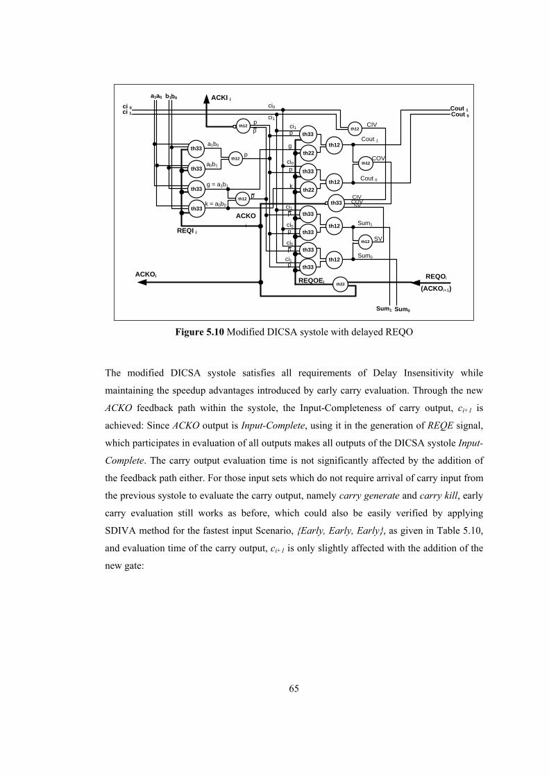
65
a0b1
a1b0
g = a1b1
k = a0b0
a1a0 b1b0
ci0
ci1
Cout 1
Cout 0
Sum1
Sum0
pth12
th12
th12
th12
(ACKOi+1)REQOEi
ACKOi
REQI i
ACKI i
p
p
p
p
p
p
p
k
g
ci1
ci0
ci0
ci0
ci1
ci1
CIV
COV
SV
CIVCOVSV
pp
ci 0ci 1
ACKOi
Cout 1Cout 0
REQOi
Sum1 Sum0
th12
th22
th12
th12
th12
th12
th12
th33
th33
th33
th33th33
th33
th33
th33
th33
th22
th33
th22
th33
Figure 5.10 Modified DICSA systole with delayed REQO
The modified DICSA systole satisfies all requirements of Delay Insensitivity while
maintaining the speedup advantages introduced by early carry evaluation. Through the new
ACKO feedback path within the systole, the Input-Completeness of carry output, ci+1 is
achieved: Since ACKO output is Input-Complete, using it in the generation of REQE signal,
which participates in evaluation of all outputs makes all outputs of the DICSA systole Input-
Complete. The carry output evaluation time is not significantly affected by the addition of
the feedback path either. For those input sets which do not require arrival of carry input from
the previous systole to evaluate the carry output, namely carry generate and carry kill, early
carry evaluation still works as before, which could also be easily verified by applying
SDIVA method for the fastest input Scenario, {Early, Early, Early}, as given in Table 5.10,
and evaluation time of the carry output, ci+1 is only slightly affected with the addition of the
new gate:
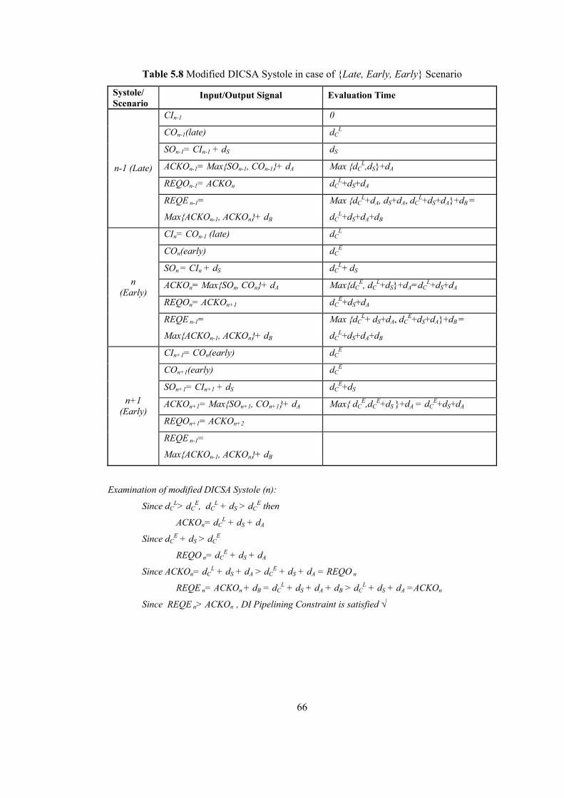
66
Table 5.8 Modified DICSA Systole in case of {Late, Early, Early} Scenario
Systole/ Scenario
Input/Output Signal Evaluation Time
CIn-1 0
COn-1(late) dCL
SOn-1= CIn-1 + dS dS
ACKOn-1= Max{SOn-1, COn-1}+ dA Max {dCL,dS}+dA
REQOn-1= ACKOn dCL+dS+dA
n-1 (Late)
REQE n-1=
Max{ACKOn-1, ACKOn}+ dB
Max {dCL+dA, dS+dA, dC
L+dS+dA}+dB =
dCL+dS+dA+dB
CIn= COn-1 (late) dCL
COn(early) dCE
SOn = CIn + dS dCL+ dS
ACKOn= Max{SOn, COn}+ dA Max{dCE, dC
L+dS}+dA=dCL+dS+dA
REQOn= ACKOn+1 dCE+dS+dA
n (Early)
REQE n-1=
Max{ACKOn-1, ACKOn}+ dB
Max {dCL+ dS+dA, dC
E+dS+dA}+dB =
dCL+dS+dA+dB
CIn+1= COn(early) dCE
COn+1(early) dCE
SOn+1= CIn+1 + dS dCE+dS
ACKOn+1= Max{SOn+1, COn+1}+ dA Max{ dCE,dC
E+dS }+dA = dCE+dS+dA
REQOn+1= ACKOn+2
n+1 (Early)
REQE n-1=
Max{ACKOn-1, ACKOn}+ dB
Examination of modified DICSA Systole (n):
Since dCL> dC
E, dCL + dS > dC
E then
ACKOn= dCL + dS + dA
Since dCE + dS > dC
E
REQO n= dCE + dS + dA
Since ACKOn= dCL + dS + dA > dC
E + dS + dA = REQO n
REQE n= ACKOn + dB = dCL + dS + dA + dB > dC
L + dS + dA =ACKOn
Since REQE n> ACKOn , DI Pipelining Constraint is satisfied √
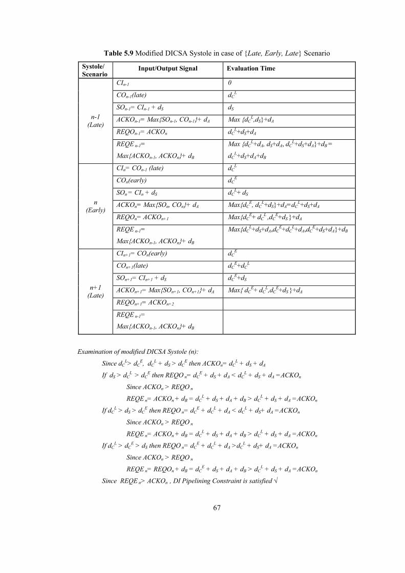
67
Table 5.9 Modified DICSA Systole in case of {Late, Early, Late} Scenario
Systole/ Scenario
Input/Output Signal Evaluation Time
CIn-1 0
COn-1(late) dCL
SOn-1= CIn-1 + dS dS
ACKOn-1= Max{SOn-1, COn-1}+ dA Max {dCL,dS}+dA
REQOn-1= ACKOn dCL+dS+dA
n-1 (Late)
REQE n-1=
Max{ACKOn-1, ACKOn}+ dB
Max {dCL+dA, dS+dA, dC
L+dS+dA}+dB =
dCL+dS+dA+dB
CIn= COn-1 (late) dCL
COn(early) dCE
SOn = CIn + dS dCL+ dS
ACKOn= Max{SOn, COn}+ dA Max{dCE, dC
L+dS}+dA=dCL+dS+dA
REQOn= ACKOn+1 Max{dCE+ dC
L ,dCE+dS }+dA
n (Early)
REQE n-1=
Max{ACKOn-1, ACKOn}+ dB
Max{dCL+dS+dA,dC
E+dCL+dA,dC
E+dS+dA}+dB
CIn+1= COn(early) dCE
COn+1(late) dCE+dC
L
SOn+1= CIn+1 + dS dCE+dS
ACKOn+1= Max{SOn+1, COn+1}+ dA Max{ dCE+ dC
L,dCE+dS }+dA
REQOn+1= ACKOn+2
n+1 (Late)
REQE n-1=
Max{ACKOn-1, ACKOn}+ dB
Examination of modified DICSA Systole (n):
Since dCL> dC
E, dCL + dS > dC
E then ACKOn= dCL + dS + dA
If dS > dCL > dC
E then REQO n= dCE + dS + dA < dC
L + dS + dA =ACKOn
Since ACKOn > REQO n
REQE n= ACKOn + dB = dCL + dS + dA + dB > dC
L + dS + dA =ACKOn
If dCL > dS > dC
E then REQO n= dCE + dC
L + dA < dCL + dS+ dA =ACKOn
Since ACKOn > REQO n
REQE n= ACKOn + dB = dCL + dS + dA + dB > dC
L + dS + dA =ACKOn
If dCL > dC
E > dS then REQO n= dCE + dC
L + dA >dCL + dS+ dA =ACKOn
Since ACKOn > REQO n
REQE n= REQOn + dB = dCE + dS + dA + dB > dC
L + dS + dA =ACKOn
Since REQE n> ACKOn , DI Pipelining Constraint is satisfied √
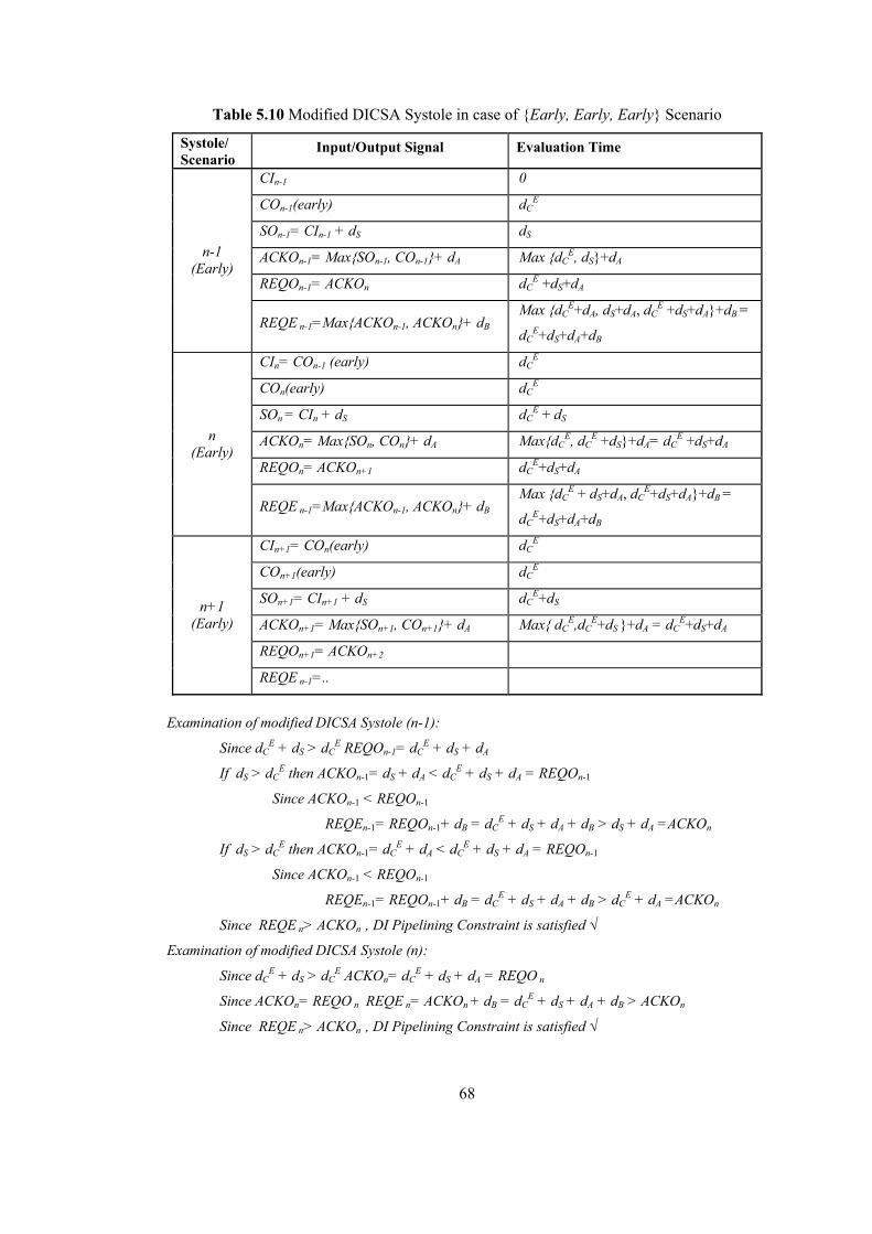
68
Table 5.10 Modified DICSA Systole in case of {Early, Early, Early} Scenario
Systole/ Scenario
Input/Output Signal Evaluation Time
CIn-1 0
COn-1(early) dCE
SOn-1= CIn-1 + dS dS
ACKOn-1= Max{SOn-1, COn-1}+ dA Max {dCE, dS}+dA
REQOn-1= ACKOn dCE +dS+dA
n-1 (Early)
REQE n-1=Max{ACKOn-1, ACKOn}+ dB Max {dC
E+dA, dS+dA, dCE +dS+dA}+dB =
dCE+dS+dA+dB
CIn= COn-1 (early) dCE
COn(early) dCE
SOn = CIn + dS dCE + dS
ACKOn= Max{SOn, COn}+ dA Max{dCE, dC
E +dS}+dA= dCE +dS+dA
REQOn= ACKOn+1 dCE+dS+dA
n (Early)
REQE n-1=Max{ACKOn-1, ACKOn}+ dB Max {dC
E + dS+dA, dCE+dS+dA}+dB =
dCE+dS+dA+dB
CIn+1= COn(early) dCE
COn+1(early) dCE
SOn+1= CIn+1 + dS dCE+dS
ACKOn+1= Max{SOn+1, COn+1}+ dA Max{ dCE,dC
E+dS }+dA = dCE+dS+dA
REQOn+1= ACKOn+2
n+1 (Early)
REQE n-1=..
Examination of modified DICSA Systole (n-1):
Since dCE + dS > dC
E REQOn-1= dCE + dS + dA
If dS > dCE then ACKOn-1= dS + dA < dC
E + dS + dA = REQOn-1
Since ACKOn-1 < REQOn-1
REQEn-1= REQOn-1+ dB = dCE + dS + dA + dB > dS + dA =ACKOn
If dS > dCE then ACKOn-1= dC
E + dA < dCE + dS + dA = REQOn-1
Since ACKOn-1 < REQOn-1
REQEn-1= REQOn-1+ dB = dCE + dS + dA + dB > dC
E + dA =ACKOn
Since REQE n> ACKOn , DI Pipelining Constraint is satisfied √
Examination of modified DICSA Systole (n):
Since dCE + dS > dC
E ACKOn= dCE + dS + dA = REQO n
Since ACKOn= REQO n REQE n= ACKOn + dB = dCE + dS + dA + dB > ACKOn
Since REQE n> ACKOn , DI Pipelining Constraint is satisfied √
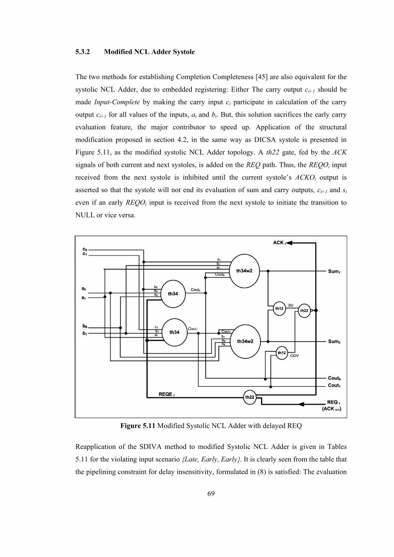
69
5.3.2 Modified NCL Adder Systole
The two methods for establishing Completion Completeness [45] are also equivalent for the
systolic NCL Adder, due to embedded registering: Either The carry output ci+1 should be
made Input-Complete by making the carry input ci participate in calculation of the carry
output ci+1 for all values of the inputs, ai and bi. But, this solution sacrifices the early carry
evaluation feature, the major contributor to speed up. Application of the structural
modification proposed in section 4.2, in the same way as DICSA systole is presented in
Figure 5.11, as the modified systolic NCL Adder topology. A th22 gate, fed by the ACK
signals of both current and next systoles, is added on the REQ path. Thus, the REQOi input
received from the next systole is inhibited until the current systole’s ACKOi output is
asserted so that the systole will not end its evaluation of sum and carry outputs, ci+1 and si
even if an early REQOi input is received from the next systole to initiate the transition to
NULL or vice versa.
Figure 5.11 Modified Systolic NCL Adder with delayed REQ
Reapplication of the SDIVA method to modified Systolic NCL Adder is given in Tables
5.11 for the violating input scenario {Late, Early, Early}. It is clearly seen from the table that
the pipelining constraint for delay insensitivity, formulated in (8) is satisfied: The evaluation
70
time of the ACK output of each systole is smaller than or equal to the evaluation time for the
REQE signal within the systole, which is generated from the ACK outputs of the current and
next systoles.
The modified Systolic NCL Adder satisfies all requirements of Delay Insensitivity while
maintaining the speedup advantages introduced by early carry evaluation. Through the new
ACK feedback path within the systole, which uses the Input-Complete ACK output in
generation of REQ signal, the Input-Completeness of carry output, ci+1 is achieved: Since
REQ participates in evaluation of all outputs. Meanwhile the carry output evaluation time is
not significantly affected by the addition of the feedback path either. For those input sets
which do not require participation of carry input from the previous systole to evaluate the
carry output, early carry evaluation still works as before, which could also be easily verified
by applying the SDIVA method for the fastest input Scenario, {Early, Early, Early}, as
given in Table 5.12, and evaluation time of the carry output, ci+1 is only slightly affected
with the addition of the new gate:
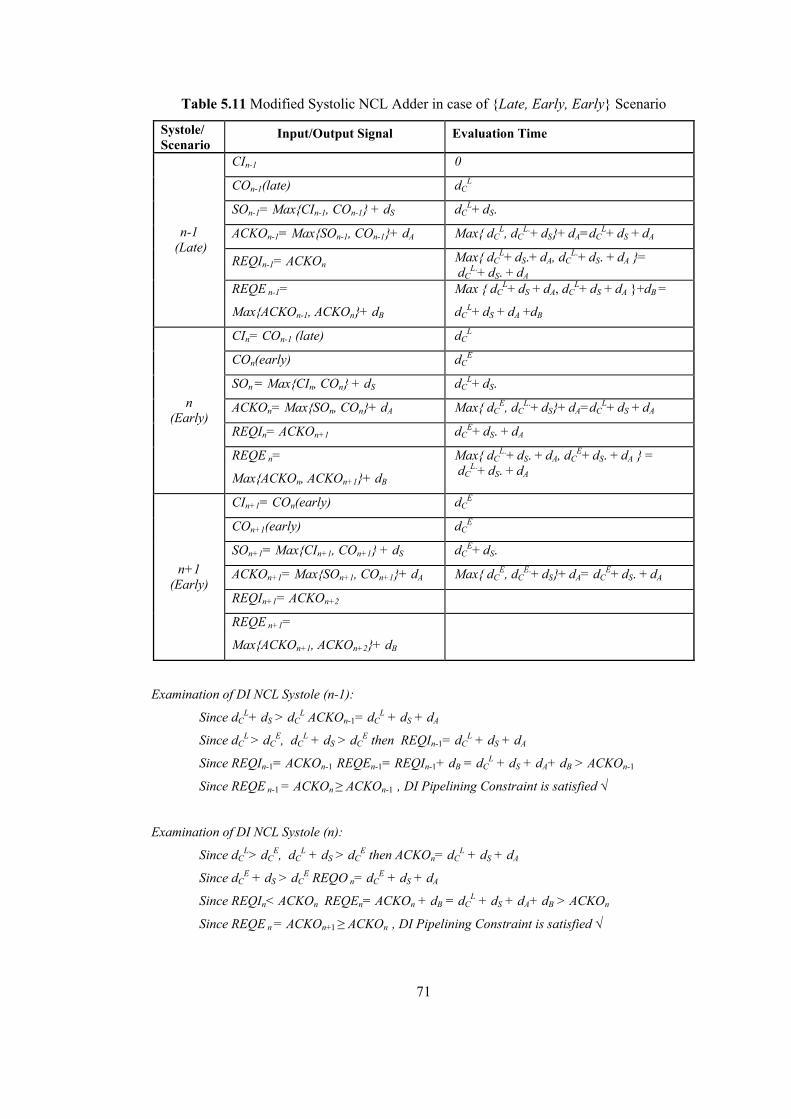
71
Table 5.11 Modified Systolic NCL Adder in case of {Late, Early, Early} Scenario
Systole/ Scenario
Input/Output Signal Evaluation Time
CIn-1 0
COn-1(late) dCL
SOn-1= Max{CIn-1, COn-1} + dS dCL+ dS.
ACKOn-1= Max{SOn-1, COn-1}+ dA Max{ dCL, dC
L.+ dS}+ dA=dCL+ dS + dA
REQIn-1= ACKOn Max{ dCL+ dS.+ dA, dC
L.+ dS. + dA }= dC
L.+ dS. + dA
n-1 (Late)
REQE n-1=
Max{ACKOn-1, ACKOn}+ dB
Max { dCL+ dS + dA, dC
L+ dS + dA }+dB =
dCL+ dS + dA +dB
CIn= COn-1 (late) dCL
COn(early) dCE
SOn = Max{CIn, COn} + dS dCL+ dS.
ACKOn= Max{SOn, COn}+ dA Max{ dCE, dC
L.+ dS}+ dA=dCL+ dS + dA
REQIn= ACKOn+1 dCE+ dS. + dA
n (Early)
REQE n=
Max{ACKOn, ACKOn+1}+ dB
Max{ dCL.+ dS. + dA, dC
E+ dS. + dA } = dC
L.+ dS. + dA
CIn+1= COn(early) dCE
COn+1(early) dCE
SOn+1= Max{CIn+1, COn+1} + dS dCE+ dS.
ACKOn+1= Max{SOn+1, COn+1}+ dA Max{ dCE, dC
E.+ dS}+ dA= dCE+ dS. + dA
REQIn+1= ACKOn+2
n+1 (Early)
REQE n+1=
Max{ACKOn+1, ACKOn+2}+ dB
Examination of DI NCL Systole (n-1):
Since dCL+ dS > dC
L ACKOn-1= dCL + dS + dA
Since dCL > dC
E, dCL + dS > dC
E then REQIn-1= dCL + dS + dA
Since REQIn-1= ACKOn-1 REQEn-1= REQIn-1+ dB = dCL + dS + dA+ dB > ACKOn-1
Since REQE n-1 = ACKOn ≥ ACKOn-1 , DI Pipelining Constraint is satisfied √
Examination of DI NCL Systole (n):
Since dCL> dC
E, dCL + dS > dC
E then ACKOn= dCL + dS + dA
Since dCE + dS > dC
E REQO n= dCE + dS + dA
Since REQIn< ACKOn REQEn= ACKOn + dB = dCL + dS + dA+ dB > ACKOn
Since REQE n = ACKOn+1 ≥ ACKOn , DI Pipelining Constraint is satisfied √
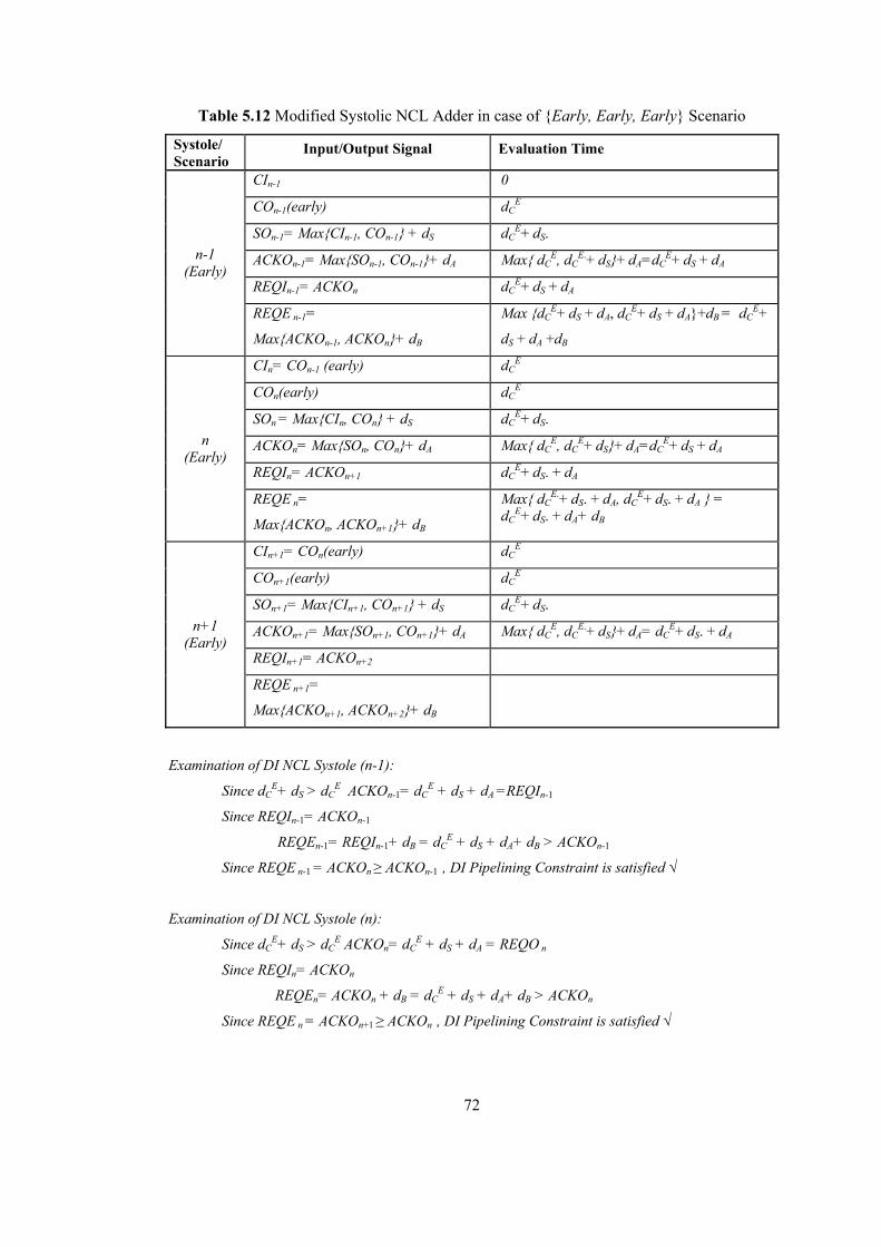
72
Table 5.12 Modified Systolic NCL Adder in case of {Early, Early, Early} Scenario
Systole/ Scenario
Input/Output Signal Evaluation Time
CIn-1 0
COn-1(early) dCE
SOn-1= Max{CIn-1, COn-1} + dS dCE+ dS.
ACKOn-1= Max{SOn-1, COn-1}+ dA Max{ dCE, dC
E.+ dS}+ dA=dCE+ dS + dA
REQIn-1= ACKOn dCE+ dS + dA
n-1 (Early)
REQE n-1=
Max{ACKOn-1, ACKOn}+ dB
Max {dCE+ dS + dA, dC
E+ dS + dA}+dB = dCE+
dS + dA +dB
CIn= COn-1 (early) dCE
COn(early) dCE
SOn = Max{CIn, COn} + dS dCE+ dS.
ACKOn= Max{SOn, COn}+ dA Max{ dCE, dC
E+ dS}+ dA=dCE+ dS + dA
REQIn= ACKOn+1 dCE+ dS. + dA
n (Early)
REQE n=
Max{ACKOn, ACKOn+1}+ dB
Max{ dCE.+ dS. + dA, dC
E+ dS. + dA } = dC
E+ dS. + dA+ dB
CIn+1= COn(early) dCE
COn+1(early) dCE
SOn+1= Max{CIn+1, COn+1} + dS dCE+ dS.
ACKOn+1= Max{SOn+1, COn+1}+ dA Max{ dCE, dC
E.+ dS}+ dA= dCE+ dS. + dA
REQIn+1= ACKOn+2
n+1 (Early)
REQE n+1=
Max{ACKOn+1, ACKOn+2}+ dB
Examination of DI NCL Systole (n-1):
Since dCE+ dS > dC
E ACKOn-1= dCE + dS + dA =REQIn-1
Since REQIn-1= ACKOn-1
REQEn-1= REQIn-1+ dB = dCE + dS + dA+ dB > ACKOn-1
Since REQE n-1 = ACKOn ≥ ACKOn-1 , DI Pipelining Constraint is satisfied √
Examination of DI NCL Systole (n):
Since dCE+ dS > dC
E ACKOn= dCE + dS + dA = REQO n
Since REQIn= ACKOn
REQEn= ACKOn + dB = dCE + dS + dA+ dB > ACKOn
Since REQE n = ACKOn+1 ≥ ACKOn , DI Pipelining Constraint is satisfied √
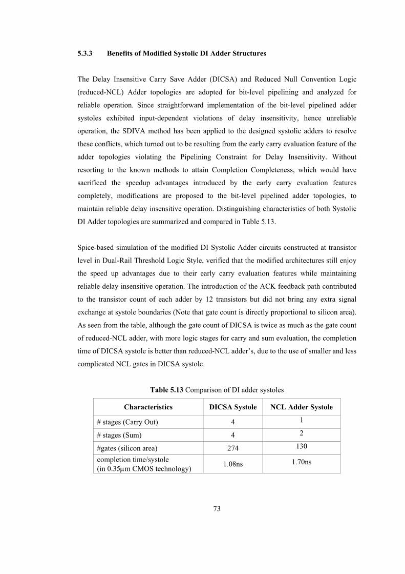
73
5.3.3 Benefits of Modified Systolic DI Adder Structures
The Delay Insensitive Carry Save Adder (DICSA) and Reduced Null Convention Logic
(reduced-NCL) Adder topologies are adopted for bit-level pipelining and analyzed for
reliable operation. Since straightforward implementation of the bit-level pipelined adder
systoles exhibited input-dependent violations of delay insensitivity, hence unreliable
operation, the SDIVA method has been applied to the designed systolic adders to resolve
these conflicts, which turned out to be resulting from the early carry evaluation feature of the
adder topologies violating the Pipelining Constraint for Delay Insensitivity. Without
resorting to the known methods to attain Completion Completeness, which would have
sacrificed the speedup advantages introduced by the early carry evaluation features
completely, modifications are proposed to the bit-level pipelined adder topologies, to
maintain reliable delay insensitive operation. Distinguishing characteristics of both Systolic
DI Adder topologies are summarized and compared in Table 5.13.
Spice-based simulation of the modified DI Systolic Adder circuits constructed at transistor
level in Dual-Rail Threshold Logic Style, verified that the modified architectures still enjoy
the speed up advantages due to their early carry evaluation features while maintaining
reliable delay insensitive operation. The introduction of the ACK feedback path contributed
to the transistor count of each adder by 12 transistors but did not bring any extra signal
exchange at systole boundaries (Note that gate count is directly proportional to silicon area).
As seen from the table, although the gate count of DICSA is twice as much as the gate count
of reduced-NCL adder, with more logic stages for carry and sum evaluation, the completion
time of DICSA systole is better than reduced-NCL adder’s, due to the use of smaller and less
complicated NCL gates in DICSA systole.
Table 5.13 Comparison of DI adder systoles
Characteristics DICSA Systole NCL Adder Systole
# stages (Carry Out) 4 1
# stages (Sum) 4 2
#gates (silicon area) 274 130
completion time/systole (in 0.35μm CMOS technology) 1.08ns 1.70ns
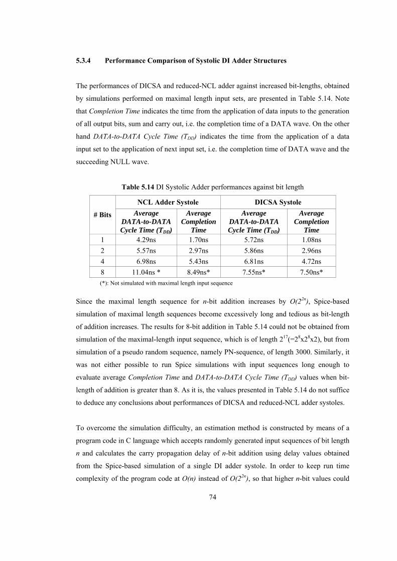
74
5.3.4 Performance Comparison of Systolic DI Adder Structures
The performances of DICSA and reduced-NCL adder against increased bit-lengths, obtained
by simulations performed on maximal length input sets, are presented in Table 5.14. Note
that Completion Time indicates the time from the application of data inputs to the generation
of all output bits, sum and carry out, i.e. the completion time of a DATA wave. On the other
hand DATA-to-DATA Cycle Time (TDD) indicates the time from the application of a data
input set to the application of next input set, i.e. the completion time of DATA wave and the
succeeding NULL wave.
Table 5.14 DI Systolic Adder performances against bit length
NCL Adder Systole DICSA Systole
# Bits Average DATA-to-DATA Cycle Time (TDD)
Average Completion
Time
Average DATA-to-DATA Cycle Time (TDD)
Average Completion
Time 1 4.29ns 1.70ns 5.72ns 1.08ns 2 5.57ns 2.97ns 5.86ns 2.96ns 4 6.98ns 5.43ns 6.81ns 4.72ns 8 11.04ns * 8.49ns* 7.55ns* 7.50ns* (*): Not simulated with maximal length input sequence
Since the maximal length sequence for n-bit addition increases by O(22n), Spice-based
simulation of maximal length sequences become excessively long and tedious as bit-length
of addition increases. The results for 8-bit addition in Table 5.14 could not be obtained from
simulation of the maximal-length input sequence, which is of length 217(=28x28x2), but from
simulation of a pseudo random sequence, namely PN-sequence, of length 3000. Similarly, it
was not either possible to run Spice simulations with input sequences long enough to
evaluate average Completion Time and DATA-to-DATA Cycle Time (TDD) values when bit-
length of addition is greater than 8. As it is, the values presented in Table 5.14 do not suffice
to deduce any conclusions about performances of DICSA and reduced-NCL adder systoles.
To overcome the simulation difficulty, an estimation method is constructed by means of a
program code in C language which accepts randomly generated input sequences of bit length
n and calculates the carry propagation delay of n-bit addition using delay values obtained
from the Spice-based simulation of a single DI adder systole. In order to keep run time
complexity of the program code at O(n) instead of O(22n), so that higher n-bit values could
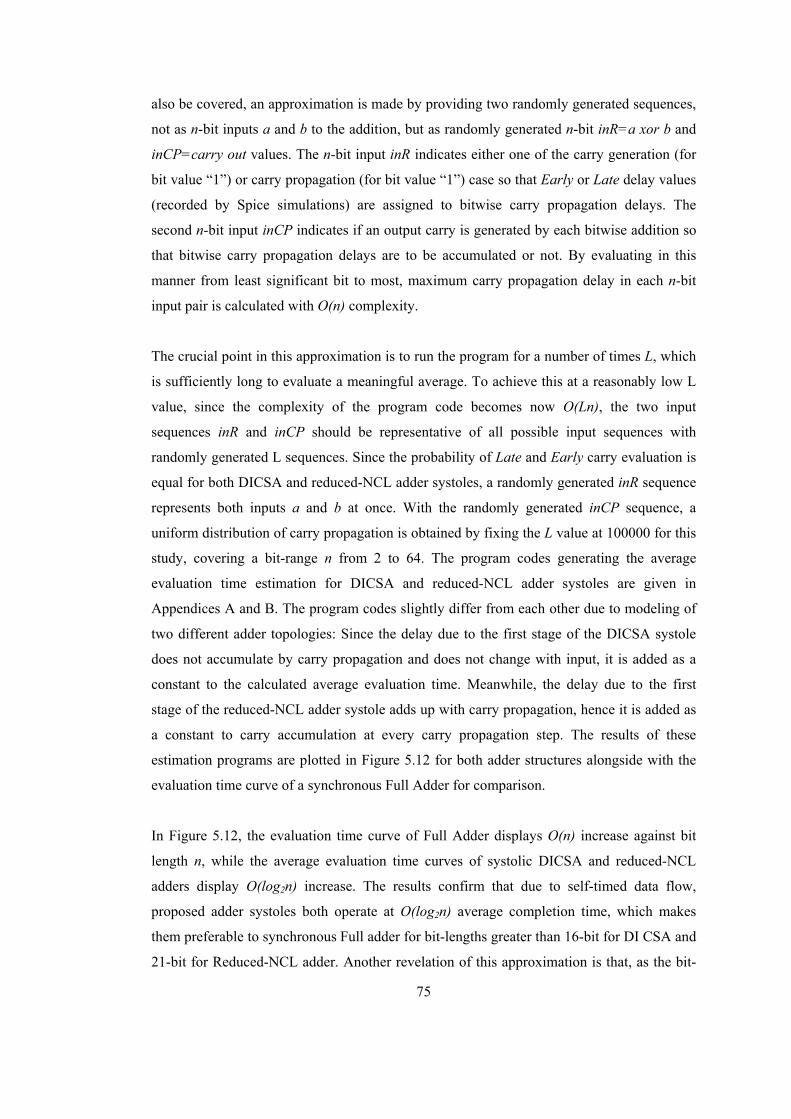
75
also be covered, an approximation is made by providing two randomly generated sequences,
not as n-bit inputs a and b to the addition, but as randomly generated n-bit inR=a xor b and
inCP=carry out values. The n-bit input inR indicates either one of the carry generation (for
bit value “1”) or carry propagation (for bit value “1”) case so that Early or Late delay values
(recorded by Spice simulations) are assigned to bitwise carry propagation delays. The
second n-bit input inCP indicates if an output carry is generated by each bitwise addition so
that bitwise carry propagation delays are to be accumulated or not. By evaluating in this
manner from least significant bit to most, maximum carry propagation delay in each n-bit
input pair is calculated with O(n) complexity.
The crucial point in this approximation is to run the program for a number of times L, which
is sufficiently long to evaluate a meaningful average. To achieve this at a reasonably low L
value, since the complexity of the program code becomes now O(Ln), the two input
sequences inR and inCP should be representative of all possible input sequences with
randomly generated L sequences. Since the probability of Late and Early carry evaluation is
equal for both DICSA and reduced-NCL adder systoles, a randomly generated inR sequence
represents both inputs a and b at once. With the randomly generated inCP sequence, a
uniform distribution of carry propagation is obtained by fixing the L value at 100000 for this
study, covering a bit-range n from 2 to 64. The program codes generating the average
evaluation time estimation for DICSA and reduced-NCL adder systoles are given in
Appendices A and B. The program codes slightly differ from each other due to modeling of
two different adder topologies: Since the delay due to the first stage of the DICSA systole
does not accumulate by carry propagation and does not change with input, it is added as a
constant to the calculated average evaluation time. Meanwhile, the delay due to the first
stage of the reduced-NCL adder systole adds up with carry propagation, hence it is added as
a constant to carry accumulation at every carry propagation step. The results of these
estimation programs are plotted in Figure 5.12 for both adder structures alongside with the
evaluation time curve of a synchronous Full Adder for comparison.
In Figure 5.12, the evaluation time curve of Full Adder displays O(n) increase against bit
length n, while the average evaluation time curves of systolic DICSA and reduced-NCL
adders display O(log2n) increase. The results confirm that due to self-timed data flow,
proposed adder systoles both operate at O(log2n) average completion time, which makes
them preferable to synchronous Full adder for bit-lengths greater than 16-bit for DI CSA and
21-bit for Reduced-NCL adder. Another revelation of this approximation is that, as the bit-
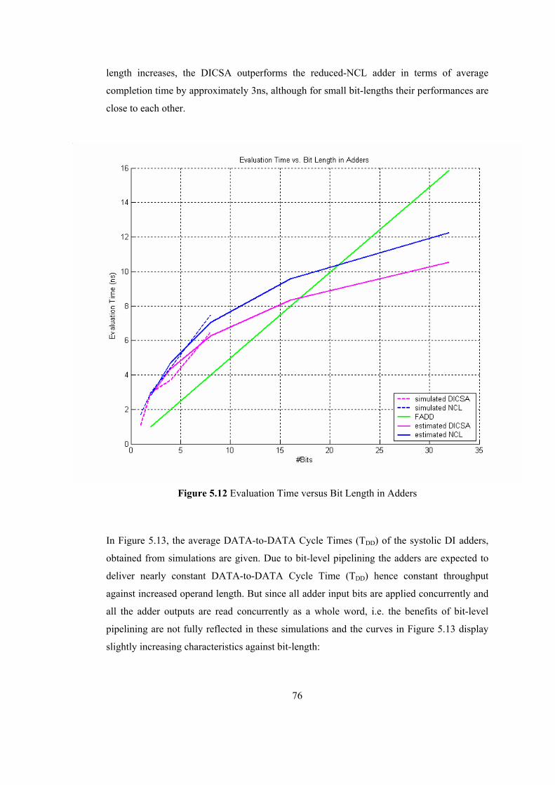
76
length increases, the DICSA outperforms the reduced-NCL adder in terms of average
completion time by approximately 3ns, although for small bit-lengths their performances are
close to each other.
Figure 5.12 Evaluation Time versus Bit Length in Adders
In Figure 5.13, the average DATA-to-DATA Cycle Times (TDD) of the systolic DI adders,
obtained from simulations are given. Due to bit-level pipelining the adders are expected to
deliver nearly constant DATA-to-DATA Cycle Time (TDD) hence constant throughput
against increased operand length. But since all adder input bits are applied concurrently and
all the adder outputs are read concurrently as a whole word, i.e. the benefits of bit-level
pipelining are not fully reflected in these simulations and the curves in Figure 5.13 display
slightly increasing characteristics against bit-length:
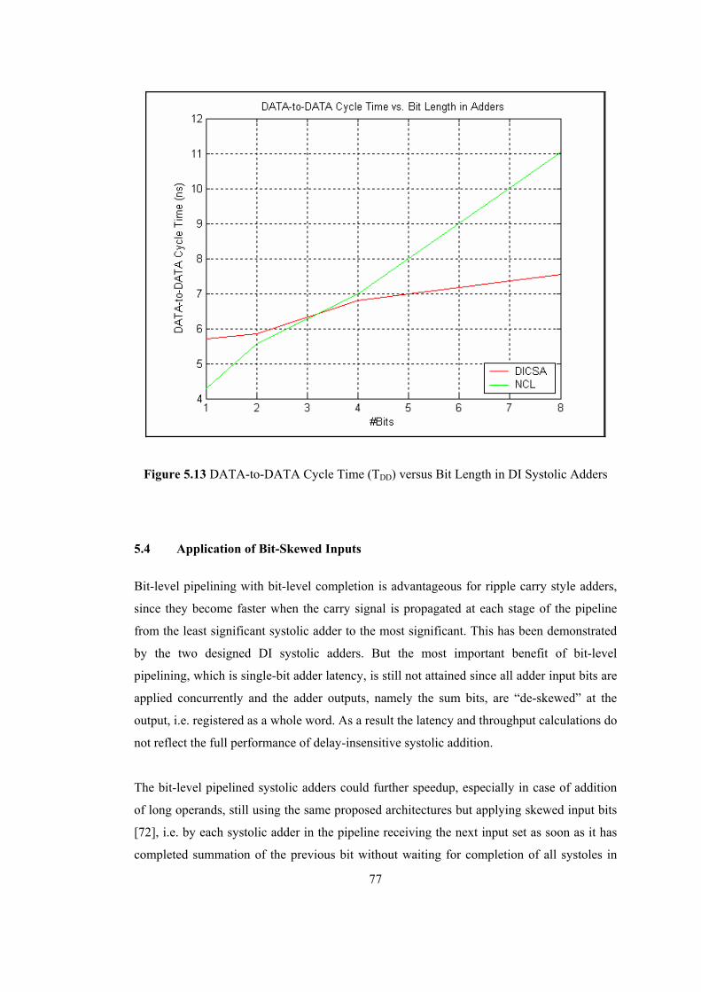
77
Figure 5.13 DATA-to-DATA Cycle Time (TDD) versus Bit Length in DI Systolic Adders
5.4 Application of Bit-Skewed Inputs
Bit-level pipelining with bit-level completion is advantageous for ripple carry style adders,
since they become faster when the carry signal is propagated at each stage of the pipeline
from the least significant systolic adder to the most significant. This has been demonstrated
by the two designed DI systolic adders. But the most important benefit of bit-level
pipelining, which is single-bit adder latency, is still not attained since all adder input bits are
applied concurrently and the adder outputs, namely the sum bits, are “de-skewed” at the
output, i.e. registered as a whole word. As a result the latency and throughput calculations do
not reflect the full performance of delay-insensitive systolic addition.
The bit-level pipelined systolic adders could further speedup, especially in case of addition
of long operands, still using the same proposed architectures but applying skewed input bits
[72], i.e. by each systolic adder in the pipeline receiving the next input set as soon as it has
completed summation of the previous bit without waiting for completion of all systoles in
78
the pipeline. For dual-rail threshold logic this would mean, each systolic adder receiving the
NULL wave as soon as its DATA wave has been processed and receiving the next DATA
wave as soon as the NULL wave has been processed as seen in Figure 5.14 This is also
called “vertical pipelining” [73] and improves the overall throughput of the systolic array.
FA(n-1)
REQ(n) ACK(n+1)
FA(n)
REQ(n+1)
Sn-10,1
REQ(n-1) ACK(n)
Sn0,1
An-10,1 Bn-1
0,1 An0,1 Bn
0,1
Cn-10
Cn-11
Cn0
Cn1 FA(n+1)
ACK(n-1)
Sn+10,1
Cn+10
Cn+11
An+10,1 Bn+1
0,1
Cn-10
Cn-11
null null
null null
null
a1 b1
null null
a2 b2
null null
null null
a2 b2
null null
a3 b3
a2 b2
a3 b3
s1
s2
null
s1
s1
null
null
null
s0
s0
s0
Figure 5.14 Bit-Skewed Inputs/Outputs in a DI Systolic Adder
5.4.1 Bit-skewed Systolic DI CSA Pipeline
The DICSA architecture reconstructed in this thesis is very suitable to benefit from vertical
pipelining. The DICSA systole could easily be adopted to receive bit-skewed inputs with its
dual-stage evaluation structure and its dedicated handshaking signals ACKI/REQI in the
data flow direction, to attain constant throughput against increased bit-length.
79
The simulation environment for the designed systolic DICSA modules has been modified to
apply inputs and receive outputs in bit-skewed fashion and exhaustive simulations have been
started with randomly generated large data sets. The first available simulation results reveal
that 27% improvement has been established in the average throughput of the 4-bit DICSA
adder while the improvement in average throughput of the 8-bit DICSA adder is currently
around 34%. The improvement in throughput is expected to increase as bit-length of the
adder increases so that almost constant throughput is attained regardless of bit-length.
5.4.2 Bit-skewed Systolic NCL Adder Pipeline
The NCL adder systole reconstructed in this thesis is also very suitable to benefit from
vertical pipelining. It could be adopted to receive bit-skewed inputs with its dual-stage
evaluation structure. Although it has only one set of handshaking signals ACK/REQ, the
same handshaking signals could control the data flow in directions, the direction of data/sum
flow and the direction of carry flow, to attain constant throughput against increased bit-
length.
5.4.3 Benefits of Bit-skewed Pipelining
The simulations performed on systolic DICSA and NCL adders confirmed that when the
environment for the designed systolic adder modules has been modified to apply inputs and
receive outputs in bit-skewed fashion, 27-34% improvement has been established in the
average throughput of the 4-bit and 8-bit systolic adders. The improvement in throughput is
expected to increase as bit-length of the adder increases so that almost constant throughput is
attained regardless of bit-length.
80
Equation Chapter 5 Section 1
CHAPTER 6 6 CONCLUSION Asynchronous circuit design style has been adapted to systolic array architectures to exploit
the benefits of both techniques, for fast, scalable and modular design. The initiative for this
study was that merging asynchronous circuit design techniques with systolic array
architectures would result in total elimination of global signal exchange which would in turn
result in an improvement of the speed and throughput of data processing. Having in mind
that the resultant circuits should be suitable for System-On-Chip design in deep sub-micron
technologies, delay-insensitive asynchronous design style has been adopted, keeping the
abstraction at logic level and employing dual-rail threshold logic gates with static
implementation as design library.
Inspired by the early carry generation related problems encountered in the design of systolic
adders, a new structural delay-insensitivity verification analysis method is proposed for
asynchronous systolic arrays in dual-rail threshold logic style. The proposed method, namely
SDIVA, employs symbolic delays for all output evaluation paths and works at the behavioral
specification level. For bit-level pipelined systolic arrays, which have data-dependent early
output evaluation in one-dimension, SDIVA method confines the verification analysis task
to examination of three adjacent systoles so that by analyzing all possible early/late output
evaluation scenarios on three systoles, the delay-insensitivity of a complete systolic array
could be verified at once, regardless of the array dimensions. This way, SDIVA achieves a
significant reduction in verification effort and time. Since the verification analysis is kept at
behavioral abstraction level using of symbolic delays and no timing constraints are imposed
on the circuit, there is no requirement to know or adjust the actual path/gate delays in the
circuit. As a result, the SDIVA method is completely independent of technology parameters
and is robust against enviromental conditions. Using the SDIVA method, also structural
modifications to the topologies offending the delay insensitivity requirements could be
devised, while maintaining early output evaluation and speed up advantages.
When compared to exsisting verification analysis methods, the SDIVA method brings
significant advantages in decreasing verification effort and also fills the void for verification
81
of pipelined structures. Formal analysis methods, being the most well-known and commonly
used verification method at behavioral abstraction level, are based on exploration of
reachable states [46] and because of this, are subject to the state space explosion problem
with increasing circuit sizes. Recent research to reduce verification complexity of
asynchronous circuits mostly target at compacting state space [53, 55] or using abstraction
[54] to reduce verification complexity, addressing State Transition Graph (STG) based
design flows such as Petrify [50]. Introducing Relative Timing Assumptions [57, 59] or
Lazy Transition System Assumptions [56, 60] are among the recent methods which
introduce timing constraints at behavioral abstraction level and test the actual delays in the
synthesized netlist against these timing constraints for verification of the delay model. Using
symbolic or parametric delays in stead of actual or relative timing constraints as presented in
[63] [64], is another method for timing abstraction, where actual delays of the circuit could
only be known after implementation. Using unspecified timing constraints represented as
symbols, a set of linear constraints which guarantee the correctness of timed transition
systems could be generated and circuit optimizations could be based on these models. For
automated design flows using dual-rail threshold logic gates such as NCL-X [51] [52], there
are recently proposed techniques for finding a compromise between circuit optimization and
reliable delay-insensitive operation. Early Evaluation and Partial Completion Methods given
in [61] and [62] respectively, both introduce relaxation of delay-insensitivity constraints for
dual-rail threshold circuits to allow for early evaluation of signals so that more optimized
and faster circuits could be synthesized without actually violating delay-insensitivity
constraints. This is achieved by distributing the early output evaluation paths within a
complex combinational circuit in such a way that the robustness of delay-insensitivity could
still be maintained in the overall circuit [61] [62] .Partitioning a dual-rail threshold logic
circuit into its control and data paths is another way to reduce delay-insensitivity analysis
complexity as proposed in [46], which tackles this problem through orphan analysis,
assuming that completion of logic operations is properly acknowledged at asynchronous
registration stages. However, all the existing delay-insensitivity verification techniques
recently developed for dual-rail threshold logic circuits address the data flow paths in the
circuit, assuming that the control parts achieving the completion detection and handshaking
mechanisms function in a delay-insensitive manner, hence leaving the problem of early or
no generation of completion acknowledgment uncovered. Besides, none of them address
pipelined structures such as systolic arrays, where the constraints for maintaining delay-
insensitivity in the control flow become more significant in determining the performance of
the circuit.
82
For demonstrating the proposed SDIVA method as well as merging of systolic array style
and asynchronous design approaches, two systolic adder architectures have been designed
and implemented in delay-insensitive asynchronous design style and constraints of delay-
insensitivity have been analyzed on them. Due to being the basic building block of signal
processing applications, and being often on the critical path, adders were chosen for this
demonstration. Two systolic delay-insensitive adders were pipelined at bit-level so that each
systole functions as a full-adder, propagating the carry signal to the next systole in row in
ripple-carry fashion. Due to the selection of adder topologies, both adders had data-
dependent early carry output evaluation which contributed greatly to the speed-up of the
system, but violated delay-insensitivity. Applying the proposed SDIVA method to these
systolic adders, these delay-insensitivity violations are detected without running extensive
simulations. Then without resorting to known methodologies which would have diminished
the early carry generation feature, the systolic adder topologies are modified to re-establish
delay insensitivity by re-applying the SDIVA method. The resultant systolic adder
topologies displayed the average case performance, O(log2n) which is expected of
asynchronous addition.
Lastly, bit-skewed input application is applied on the designed delay-insensitive systolic
adders to further enhance the speed up issues and to boost their performance up to the
constant throughput limit which is expected from bit-level pipelining. This method was
expected to compensate for the excess processing delay introduced by the NULL cycles in
dual-rail threshold logic implementation style by vertical pipelining the input and output
registration stages of the adders. The obtained results pointed to 27-34% improvement in
completion time of addition .
The most promising part of the thesis study, which could have a potential for future
improvement is the proposed Structural Delay Insensitivity Verification Analysis method
SDIVA. It is a new technique directly targeting systolic array style architectures. And it also
differs from other verification methods using symbolic delays in one major aspect: It does
not impose any timing constraints on the environment, so there is no need for verification of
the environment against any timing assumptions after implementation. The use of symbolic
delays provides a degree of timing abstraction which makes this technique very handy to be
re-applied during circuit optimizations. Since exact delay values are not required to apply
the SDIVA technique, technology migration is also easier.
83
The SDIVA method could also be extended to systolic arrays which have early output
evaluation paths in two-dimensions or multiple early evaluating outputs in one-dimension.
In a two-dimensional systolic array, each systole has interaction with 4 to 8 neighboring
systoles depending on the functionality. At worst case, i.e. if a systole has interaction with 8
neighbors, the delay-insensitivity analysis of the entire array could be reduced to
examination of nine adjacent systoles and 29 early/late output evaluation scenarios on a nine-
systole cluster, which is still a significant reduction in verification analysis cost, especially
when compared to formal analysis methods. This technique could be very useful in design
and verification of pipelined data processing systems in general, such as filters, crypto-
processers, image processers, so that verification of a regular systolic architecture could be
performed by analysing a single systole and its neighbours which exchange signals with that
systole.
A possible future utilization of the SDIVA method could be embedding it into automated
CAD tools for verification of delay-insensitivity .
84
BIBLIOGRAHPY [1]. C. Maxfield, “To be or not to be asynchronous; that is the question”, EDN, December 7, 1995.
[2]. S. B. Furber, “The Return of Asynchronous Logic”, URL http://intranet.cs.man.ac.uk/apt/async/background/return_async.html, October 2007, Last Accessed in April 2008.
[3]. S. Hauck, “Asynchronous Design Methodologies: An Overview”, Proceedings of the IEEE, Vol. 83, No. 1, pp. 69-93, January 1995.
[4]. ACiD WG Home Page (Working Group on Asynchronous Circuit Design, funded by European Commission), URL http://www.bcim.lsbu.ac.uk/ccsv/ACiD-WG, July 2005, Last Accessed in April 2008.
[5]. D. A. Edwards, W. B. Toms, “The Status of Asynchronous Design in Industry”, IST Programme Concerted Action Thematic Network Contract, IST-1999-29119, 2nd Edition, January 2003.
[6]. C. H. van Berkel, M. B. Josephs, S. M. Nowick, “Scanning the Technology: Applications of Asynchronous Circuits”, Proceedings of the IEEE, Vol. 87, Issue 2, pp. 223-233, February, 1999.
[7]. D. A. Edwards, W. B. Toms, “Design, Automation and Test for Asynchronous Circuits and Systems”, IST Programme Concerted Action Thematic Network Contract, IST-1999-29119, 2nd Edition, January 2003.
[8]. “International Technology Roadmap for Semiconductors”, 2001 Edition, SIA, URL http://www.itrs.net/Links/2001ITRS/Home.htm, January 2008, Last Accessed in April 2008.
[9]. M. Kishinevsky, L. Lavagno, P. Vanbekberen, “The Systematic Design of Asynchronous Circuits”, ICCAD’95 Tutorial.
[10]. N.H.E. Weste, K. Esraghian, “Principles of CMOS VLSI Design, A Systems Perspective”, Addison-Wesley, 2nd Edition, 1993.
[11]. T. J. Chaney, C. E. Molnar, “Anomalous Behavior of Synchronizers and Arbiters”, IEEE Transactions on Computers, vol. C-22, pp. 421-422, Apr. 1973.
[12]. M. Reanaudin, “Asynchronous System Design”, TIMA Lab Research Reports, ISRN TIMA--RR-02/03-01—FR, Communication to MEDEA Conference, Eindhoven, October, 2001.
[13]. M. J. G. Lewis, “Low Power Asynchronous Digital Signal Processing”, PhD Thesis, Faculty of Science and Engineering, University of Manchester, October, 2000.
[14]. W.J. Bainbridge, “Asynchronous System-On-Chip Interconnect”, PhD Thesis,
85
Faculty of Science and Engineering, University of Manchester, March, 2000.
[15]. A. Bardsley, “Implementing BALSA Handshake Circuits”, PhD Thesis, Faculty of Science and Engineering, University of Manchester, 2000.
[16]. K. M. Fant, S. A. Brandt, “NULL Convention LogicTM Systems”, US Patent, 5305463, April, 1994.
[17]. I. E. Sutherland, “Micropipelines”, Communications of the ACM, 32 (6), pp 720-738, June 1989.
[18]. APT Group, University of Manchester, UK, “The AMULET3 Processor”, URL http://intranet.cs.man.ac.uk/apt/projects/processors/amulet/AMULET3_uP.php, July 2005, Last Accessed in April 2008.
[19]. A. Takamura, M. Kuwakao, M. Imai, T. Fujii, M. Ozawa, I. Fukasaku, Y. Ueno, T. Nanya, “TITAC-2: A 32-bit Scalable-Delay-Insensitive Microprocessor”, Proceedings of ICCD’97, pp 288-294, October, 1997.
[20]. M. Singh, J.A. Tierno, A. Rylyakov, S. Rylov, S.M. Nowick, “An Adaptively-Pipelined Mixed Synchronous-Asynchronous Digital FIR Filter Chip Operating at 1.3 GigaHertz”, Proceedings of 8th International Symposium on Asynchronous Circuits and Systems, pp.84-98, April, 2002.
[21]. E. Allier, G. Sicard, L. Fesquet, M. Renaudin, “A New Class of Asynchronous A/D Converters Based on Time Quantization”, Proceedings of 9th International Symposium on Asynchronous Circuits and Systems, pp.196-205, May, 2003.
[22]. G. M. Jacobs, R. B. Brodersen, “A Fully Asynchronous Digital Signal Processor Using Self-Timed Circuits”, IEEE Journal of Solid State Circuits, Vol. 25, No. 6, pp.1526-1537, December, 1990.
[23]. S. Moore, R. Anderson, P. Cunningham, R. Mullins, and G. Taylor, “Improving Smart Card Security Using Self-Timed Circuits”, Proceedings of 8th International Symposium on Asynchronous Circuits and Systems, pp.211-218, April, 2002.
[24]. J. Kessel, G. Besten, V. Peeters, T. Kramer, “Applying Asynchronous Circuits in Contactless Smart Cards”, Proceedings of 6th International Symposium on Asynchronous Circuits and Systems, pp.36-44, April, 2000.
[25]. F. Robin, M. Renaudin, G. Privat, N. Van Den Bossche “Functionally Asynchronous Array For Morphological Filtering of Greyscale Images”, IEE Proceedings, Vol. 143, No. 5, pp.273-281, September, 1996.
[26]. D. P. Thompson, A. M. Peacock, D. Renshaw, G. A. Allan, “Asynchronous Filter Banks for Discrete Wavelet Transform”, Electronic Letters, Vol. 37, No. 15, pp.983-884, July, 2001.
[27]. D. Lattard, G. Mazzare, “Image Reconstruction Using an Original Asynchronous Cellular Array”, Proceedings of International Symposium on Circuits and Systems, 1989.
[28]. C. E. C. Rayes, J. D. Brugera, “VLSI Systolic Array Architecture for the Lattice
86
Structure of the Discrete Wavelet Transform”, Proceedings of the International Symposium on Circuits and Systems, Vol. 4, pp.605-608, May 2000.
[29]. H. Saito, A. Kondratyev, J. Cortadella, L. Lavagno, A. Yakovlev, “What is the cost of delay insensitivity?”, 1999 IEEE/ACM International Conference on Computer-Aided Design, Digest of Technical Papers, 7-11 Nov. 1999, pp. 316–323.
[30]. S. C. Smith, “Gate and Throughput Optimizations for NULL Convention Self-Timed Digital Circuits”, Ph.D. Dissertation, School of Electrical Engineering and Computer Science, University of Central Florida, May 2001.
[31]. D. E. Muller, “Asynchronous Logics and Application to Information Processing”, Switching Theory in Space Technology, Stanford University Press, pp. 289-297, 1963.
[32]. T. S. Anantharaman, “A Delay Insensitive Regular Expression Recognizer”, IEEE VLSI Technology Bulletin, Sept. 1986.
[33]. J. Sparso, J. Staunstrup, M. Dantzer-Sorensen, “Design of Delay Insensitive Circuits using Multi-Ring Structures”, Proceedings of the European Design Automation Conference, pp. 15-20, 1992.
[34]. N. P. Singh, “A Design Methodology for Self-Timed Systems”, Master’s Thesis, MIT/LCS/TR-258, Laboratory for Computer Science, MIT, 1981.
[35]. Ilana David, Ran Ginosar, and Michael Yoeli, “An Efficient Implementation of Boolean Functions as Self-Timed Circuits”, IEEE Transactions on Computers, Vol. 41, No. 1, pp. 2-10,1992.
[36]. A. J. Martin, “Compiling Communicating Processes into Delay-Insensitive VLSI Circuits,” Distributed Computing, Vol. 1, No. 4, pp. 226-234, 1986.
[37]. A. J. Martin, A. Lines, R. Manohar, M. Nystrom, P. Penzes, R. Southworth, U. Cummings, and Tak Kwan Lee, “The Design of an Asynchronous MIPS R3000 Microprocessor,” Proceedings of the 17th Conference on Advanced Research in VLSI, pp. 164-181, 1997.
[38]. A. J. Martin, S. M. Burns, T. K. Lee, D. Borkovic, and P. J. Hazewindus, “The Design of an Asynchronous Microprocessor,” Advanced Research in VLSI: Proceedings of the Decennial Caltech Conference on VLSI, pp. 351-373, 1989.
[39]. K. M. Fant, S. A. Brandt, “NULL Convention LogicTM”, Theseus Logic Inc. White Paper, 1997.
[40]. K. M. Fant, S. A. Brandt, “NULL Convention LogicTM : A Complete and Consistent Logic for Asynchronous Digital Circuit Synthesis”, Proceedings of International Conference on Applications Specific Systems, Architectures and Processors (ASAP’96), pp. 261-273, 19-21 August 1996.
[41]. G. E. Sobelman, K. M. Fant, “CMOS Circuit Design of Threshold Gates with Hysteresis”, Proceedings of IEEE International Conference Circuits and Systems (ISCAS’98), Vol. 2, pp. 61-64, 31 May-3 June 1998.
87
[42]. S. C. Smith, R. F. DeMara, J. S. Yuan, M. Hagedorn, and D. Ferguson, “Delay-Insensitive Gate-Level Pipelining”, Integration, the VLSI Journal, Vol. 30/2, pp. 103-131, October 2001.
[43]. J. Cortadella, A. Kondratyev, L. Lavagno, C. Sotiriou, “Coping with the variability of combinational logic delays”, Proceedingsof the IEEE International Conference on Computer Design: VLSI in Computers and Processors, 2004, ICCD 2004, Page(s): 505- 508, 11-13 Oct. 2004.
[44]. C. L. Seitz, “System Timing,” Introduction to VLSI Systems, Addison-Wesley, pp. 218-262, 1980.
[45]. S.C. Smith, “Completion-Completeness for NULL Convention Digital Circuits Utilizing the Bitwise Completion Strategy”, The 2003 International Conference on VLSI, pp. 178-184, June 2003.
[46]. A. Kondratyev, L. Neukom, O. Roig, A. Taubin, K. Fant, “Checking delay-insensitivity: 104 gates and beyond”, Proceedings of Eighth International Symposium on Asynchronous Circuits and Systems 2002, 8-11 April 2002, pp. 149-157.
[47]. M. A. Franklin, T. Pan, “Performance comparison of asynchronous adders”, Proceedings of International Symposium on Advanced Research in Asynchronous Circuits and Systems 1994, 3-5 Nov 1994, pp. 117-125.
[48]. T. A. Chu, C. K. C. Leung, T. S. Wanuga, “A Design Methodology for Concurrent VLSI Systems”, Proceedings of ICCD, pp. 407-410, 1985.
[49]. T. A. Chu, “Synthesis of Self-timed VLSI Circuits from Graph-Theoretic Specifications”, M.I.T. Tech. Rep. MIT/LCS/TR-393, June 1987.
[50]. J. Cortadella, M. Kishinevsky, A. Kondratyev, L. Lavagno, and A.Yakovlev, “Petrify: A tool for manipulating concurrent specifications and synthesis of asynchronous controllers,” IEICE Transactions on Information Systems, vol. E80-D, pp. 315–325, Mar. 1997.
[51]. M. Ligthart, K. Fant, R. Smith, A. Taubin, and A. Kondratyev, “Asynchronous design using commercial HDL synthesis tools”, Proceedings of the International Symposium on Advanced Research in Asynchronous Circuits and Systems, pp. 114-125. IEEE Computer Society Press, Apr. 2000.
[52]. A. Kondratyev and K. Lwin, “Design of asynchronous circuits using synchronous CAD tools”, IEEE Design & Test of Computers, 19(4):107-117, 2002.
[53]. A. Valmari, “Stubborn Sets for Reduced State Space Generation”, Advances in Petri Nets 1990, Lecture Notes in Computer Science, 483, pp. 491-515.
[54]. P. Godefroid, “Partial-Order Methods for the Verification of Concurrent Systems --An Approach to the State-Explosion Problem”, Lecture Notes in Computer Science, 1032, January 1996.
[55]. E.M. Clarke, O. Grumberg, and D.E. Long, “Model checking and abstraction”, Proceedings of the Nineteenth Annual ACM Symposium on Principles of Programming
88
Languages, January 1992.
[56]. J. Cortadella, M. Kishinevsky, A. Kondratyev, L. Lavagno, A. Taubin, A. Yakovlev, “Lazy transition systems: application to timing optimization of asynchronous circuits”, Proceedings of the IEEE/ACM International Conference on Computer-Aided Design, 1998, ICCAD 98. Digest of Technical Papers. 1998, pp. 324- 331, 8-12 Nov 1998.
[57]. K. Stevens, R. Ginosar, S. Rotem, “Relative timing”, Proceedings of the Fifth International Symposium on Advanced Research in Asynchronous Circuits and Systems, 1999. pp. 208-218, 1999.
[58]. K. Stevens, R. Ginosar, S. Rotem, “Relative timing”, IEEE Transactions on Very Large Scale Integration (VLSI) Systems, Volume: 11 Issue: 1, pp. 129- 140, Feb 2003.
[59]. J. Cortadella, M. Kishinevsky, S.M. Burns, K. Stevens, “Synthesis of asynchronous control circuits with automatically generated relative timing assumptions”, Computer-Aided Design, 1999. Digest of Technical Papers. 1999 IEEE/ACM International Conference on, pp. 324-331, 1999.
[60]. J. Cortadella, M. Kishinevsky, S.M. Burns, A. Kondratyev, L. Lavagno, K. Stevens, A. Taubin, A. Yakovlev, “Lazy transition systems and asynchronous circuit synthesis with relative timing assumptions”, IEEE Transactions on Computer-Aided Design of Integrated Circuits and Systems, Volume: 21 Issue: 2, pp. 109-130, Feb 2002.
[61]. Zhou Yu, D Sokolov, A. Yakovlev, “Cost-aware synthesis of asynchronous circuits based on partial acknowledgement”, Computer-Aided Design, 2006. ICCAD '06. IEEE/ACM International Conference on, pp. 158-163, Nov. 2006.
[62]. C. Jeong,; S. M. Nowick, “Optimization of Robust Asynchronous Circuits by Local Input Completeness Relaxation”, Proceedings of the Asia and South Pacific Design Automation Conference 2007, ASP-DAC '07., pp. 622-627, Jan. 2007.
[63]. R. Clariso, J. Cortadella, “Verification of timed circuits with symbolic delays”, Proceedings of the Asia and South Pacific Design Automation Conference, 2004, ASP-DAC 2004, pp. 628- 633, 27-30 Jan. 2004.
[64]. R. Clariso, J. Cortadella, “Verification of concurrent systems with parametric delays using octahedral”, Proceedings of the Fifth International Conference on Application of Concurrency to System Design, 2005, ACSD 2005, pp. 122- 131, 7-9 June 2005.
[65]. Çetin Kaya Koç, “RSA Hardware Implementation”, Copyright©RSA Laboratories, Version 1.0, August 1995.
[66]. S. Yeşil, A. N. İsmailoğlu, Y. Ç. Tekmen, M. Aşkar, “Two Fast RSA Implementations using High-Radix Montgomery Algorithm”, Proceedings of the IEEE International Symposium on Circuits and Systems (ISCAS’2004), Vancouver, Canada, May 23-36, 2004.
[67]. P. L. Montgomery, “Modular Multiplication Without Trial Division”, Mathematics of Computations, Vol.44, pp.519-521, 1985.
[68]. S. C. Smith, R. F. DeMara, J. S. Yuan, D. Ferguson, and D. Lamb, "Optimization of
89
NULL Convention Self-Timed Circuits," Integration, The VLSI Journal, Vol. 37/3, pp. 135-165, August 2004.v
[69]. A. Tubin, K. Mred . Fant, J. McCardle, “Design of Delay Insensitive Three Dimension Pipeline Array Multiplier”, Proceedings of IEEE International Conference on Computer Design: VLSI in Computer and Processors 2002, pp. 104-111, 16-18 September 2002.
[70]. S.K. Bandapati, S.C. Smith, M.Choi, “Design and Characterization of Null Convention Self-Timed Multipliers”, IEEE Design and Test of Computers, pp. 26-35, November-December 2003.
[71]. S. C. Smith, "Development of a Large Word-Width High-Speed Asynchronous Multiply and Accumulate Unit," Integration, The VLSI Journal, Vol. 39/1, pp. 12-28, September 2005.
[72]. U. V. Cummings, A. M. Lines, A. J. Martin, “An Asynchronous Pipeline Lattice-Structure Filter”, Proceedings of International Symposium on Advanced Research in Asynchronous Circuits and Systems, pp. 126-133, IEEE Computer Society Press, 1994.
[73]. C. Brej, “Early Output Logic and Anti-tokens,” PhD. Thesis, University of Manchester, UK, September 2005.
[74]. A. N. Ismailoglu, M. Aşkar, “Application of Bit-level Pipelining to Delay Insensitive Null Convention Adders”, Proceedings of the IEEE International Symposium on Circuits and Systems (ISCAS’2007), pp. 3259-3262, May 2007.
90
APPENDIX A: C Code for DICSA Estimation
#include<stdio.h> #include<stdlib.h> #include<math.h> void char2bin (unsigned char* , unsigned char* , int ); FILE *inCP; FILE *inR; int main() { int R, N, L; int i, m; unsigned char* dR; unsigned char* dCP; unsigned char* binR; unsigned char* binCP; double* dX; double dxa; double dCS; double dACC, dAVE;
printf("\nEnter the number of binary digits: \n"); scanf("%d", &N); L = 100000; printf("\nLength of the sequence to be generated: %d\n", L); if ( ( inCP = fopen("randCP.dat","r") ) == NULL )
{ printf("\n Can't open file for input\n\n"); exit(-1);
} if ( ( inR = fopen("randR.dat","r") ) == NULL )
{ printf("\n Can't open file for input\n\n"); exit(-1);
} dR = (unsigned char*) malloc ( N*sizeof(unsigned char)); dCP = (unsigned char*) malloc ( N*sizeof(unsigned char)); binR = (unsigned char*) malloc ( N*sizeof(unsigned char)); binCP = (unsigned char*) malloc ( N*sizeof(unsigned char)); dX = (double*) malloc ( N*sizeof(double));
91
dACC = 0;
for (i=0; i<L; i++) {
fscanf(inR,"%s", dR); char2bin(dR, binR, n);
fscanf(inCP,"%s", dCP); char2bin(dCP, binCP, n);
dxa = 0; for (m=0; m<n; m++) { if (binR[m]==0) { dX[m] =2.2915; // delay of EARLY Carry Outpu of DICSA } else if (binR[m]==1) { dX[m] =2.293; // delay of LATE Carry Output of DICSA } else printf("\nerror!!\n"); } dCS=0; for (m=0; m<n; m++) { if (binCP[m]) dxa = 0; else { dxa = dxa + dX[m]; dCS = (dxa > dCS) ? dxa : dCS; } } dACC = dACC + dCS; }
dAVE = dACC/L; dAVE = dAVE + 0.5 ;// add propagation delay for first stage of DICSA systole
printf("\n%f\n", dAVE); fclose(inCP); fclose(inR);
} void char2bin (unsigned char* cnum, unsigned char* bnum, int blen){ int b;
for (b=0; b<blen; b++) { if (cnum[b] == '0')
bnum[b] = 0; else if (cnum[b] == '1')
bnum[b] = 1; else printf("\nerror!!\n"); }
}

92
APPENDIX B: C Code for DI NCL Adder Estimation
#include<stdio.h> #include<stdlib.h> #include<math.h> void char2bin (unsigned char* , unsigned char* , int ); FILE *inCP; FILE *inR; int main() { int R, N, L; int i, m; unsigned char* dR; unsigned char* dCP; unsigned char* binR; unsigned char* binCP; double* dX; double dxa; double dCS; double dACC, dAVE;
printf("\nEnter the number of binary digits: \n"); scanf("%d", &N); L = 100000; printf("\nLength of the sequence to be generated: %d\n", L); if ( ( inCP = fopen("randCP.dat","r") ) == NULL )
{ printf("\n Can't open file for input\n\n"); exit(-1);
} if ( ( inR = fopen("randR.dat","r") ) == NULL )
{ printf("\n Can't open file for input\n\n"); exit(-1);
} dR = (unsigned char*) malloc ( N*sizeof(unsigned char)); dCP = (unsigned char*) malloc ( N*sizeof(unsigned char)); binR = (unsigned char*) malloc ( N*sizeof(unsigned char)); binCP = (unsigned char*) malloc ( N*sizeof(unsigned char)); dX = (double*) malloc ( N*sizeof(double));
93
dACC = 0;
for (i=0; i<L; i++) {
fscanf(inR,"%s", dR); char2bin(dR, binR, n);
fscanf(inCP,"%s", dCP); char2bin(dCP, binCP, n);
dxa = 0; for (m=0; m<n; m++) { if (binR[m]==0) { dX[m] = 2.16; // delay of EARLY Carry Output of NCL Add } else if (binR[m]==1) { dX[m] = 2.42; // delay of LATE Carry Output of NCL Add } else printf("\nerror!!\n"); } dCS=0; for (m=0; m<n; m++) { if (binCP[m]) dxa = 0; else { dxa = dxa + dX[m] + 0.5; // add propagation delay for
// ACK generation in NCL Adder dCS = (dxa > dCS) ? dxa : dCS; } } dACC = dACC + dCS; }
dAVE = dACC/L; dAVE = dAVE +
printf("\n%f\n", dAVE); fclose(inCP); fclose(inR);
} void char2bin (unsigned char* cnum, unsigned char* bnum, int blen){ int b;
for (b=0; b<blen; b++) { if (cnum[b] == '0')
bnum[b] = 0; else if (cnum[b] == '1')
bnum[b] = 1; else printf("\nerror!!\n");}
}

94
CURRICULUM VITAE
PERSONAL INFORMATION
Surname, Name: İsmailoğlu, A. Neslin
Nationality: Turkish (TC)
Date and Place of Birth: 6th September 1969, Adana
Marital Status: Single
Phone: +90 312 210 13 10 / 1141
Fax: +90 312 210 13 15
email: [email protected]
EDUCATION
Degree Institution Year of Graduation
MS METU Electrical & Electronics Engineering 1995
BS METU Electrical & Electronics Engineering 1991
High School Ankara Science High School 1987
WORK EXPERIENCE
Year Place Enrollment
1996 – Present TÜBİTAK UZAY (formerly BİLTEN) Senior Researcher,
Coordinator,
Project Manager
1991-1996 ASELSAN – MST Group Design Engineer
FOREIGN LANGUAGES
Advanced English, Average Italian
RECENT PUBLICATIONS
N. İsmailoğlu, M. Aşkar, “Application of Bit-level Pipelining to Delay Insensitive Null
Convention Adders”, Proceedings of ISCAS 2007: IEEE International Symposium on
Circuits and Systems, pp. 3259-3262, New Orleans, U.S.A., 27-30 May 2007.
95
N. İsmailoğlu, O. Benderli, S. Yeşil, R. Sever, B. Okcan, O. Şengül, R. Öktem, “GEZGİN &
GEZGİN-2: Adaptive Real-Time Image Processing Subsystems for Earth-Observing Small
Satellites”, Proceedings of 1st NASA/ESA Conference on Adaptive Hardware and Systems
(AHS 2006) Conference, İstanbul, 15-18 June 2006.
N. İsmailoğlu, O. Benderli, R. Öktem, “Improving Compression Ratio for Satellite
Transmission by use of Cloud Extraction”, Proceedings of 13th European Signal processing
Conference (EUSIPCO 2005) Conference, Antalya, 4-8 Sept. 2005.
N. İsmailoğlu, O. Benderli, S. Yeşil, R. Sever, B. Okcan, R. Öktem, “GEZGİN-2: An
Advanced Image Processing Subsystem for Earth-Observing Small Satellites”, Proceedings
of Recent Advances in Space Technologies (RAST 2005) Conference, İstanbul, 9-11 June
2005.
N. İsmailoğlu, S. Yeşil, R. Sever, B. Okcan, “GÖLGE: A Case Study of a Secure Data
Communication Subsystem for Micro-Satellites”, Proceedings of Recent Advances in Space
Technologies (RAST 2005) Conference, İstanbul, 9-11 June 2005.
N. İsmailoğlu, O. Şen, H. Sunay, C. Dudak, T. Kırılmaz, “High Data Rate X-Band
Transmitter For Low Earth Orbit Satellites“,Proceedings of ESA Small Satellite Systems &
Services Symposium (4S) Conference, La Rochelle, France, 20-24 Sept. 2004.
N. İsmailoğlu, R. Sever, Ç. Tekmen, M. Aşkar, “A High Speed ASIC Implementation of
The Rijndael Algorithm”, Proceedings of IEEE International Symposium on Circuits and
Systems (ISCAS’2004), Vancouver, Canada, 23-26 May 2004..
N. İsmailoğlu, S. Yeşil, Ç. Tekmen, M. Aşkar, “Two Fast RSA Implementations Using
High-Radix Montgomery Algorithm”, Proceedings of IEEE International Symposium on
Circuits and Systems (ISCAS’2004), Vancouver, Canada, 23-26 May 2004.
N. İsmailoğlu, O. Şen, H. Sunay, C. Dudak, T. Kırılmaz, “A High Data Rate X-Band
Transmitter”, ESA Microwave Technology and Techniques Workshop Preparing for Future
Space Systems, Noorwijk, Netherlands, 11-12 May 2004.
96
N. İsmailoğlu, O. Benderli, I. Korkmaz, S. Yeşil, R. Sever, H. Sunay, T. Kolçak, Ç. Tekmen,
“GEZGİN: A Case Study of a Real-time Image Processing Sub-system for Micro Satellites”,
Proceedings of Recent Advances in Space Technologies (RAST 2003) Conference, İstanbul,
20-22 Nov. 2003.
N. İsmailoğlu, O. Benderli, Ç. Tekmen, “Real Time, Low Latency, Architecture for the 2-D
Discrete Wavelet Transformation For Streaming Image Applications”, Proceedings of IEEE
Workshop on Signal Processing Systems Conference, Seul, S. Korea, 27-29 August 2003.
N. İsmailoğlu, O. Benderli, Ç. Tekmen, “Real Time, Low Latency, FPGA Implementation
of the 2-D Discrete Wavelet Transformation For Streaming Image Applications”,
Proceedings of EUROMICRO Symposium on Digital System Design, Antalya, 2-5
September 2003.
N. İsmailoğlu, O. Benderli, I. Korkmaz, M. Durna, T. Kolçak and Y. Ç. Tekmen, “A Real
Time Image Processing Subsystem: GEZGIN”, Proceedings of 16th AIAA/USU Conference
on Small Satellites Conference, Utah, U.S.A., August 2002.
HOBBIES
Sports (ski, tennis, basketball, mountain-bike, swimming), Yoga, Film Analysis, Rock
Music, Travelling.