Embed Size (px)
Citation preview
TL16C750ASYNCHRONOUS COMMUNICATIONS ELEMENT
WITH 64-BYTE FIFOs AND AUTOFLOW CONTROLSLLS191C – JANUARY 1995 – REVISED DECEMBER 1997
1POST OFFICE BOX 655303 • DALLAS, TEXAS 75265
Pin-to-Pin Compatible With the ExistingTL16C550B/C
Programmable 16- or 64-Byte FIFOs toReduce CPU Interrupts
Programmable Auto-RTS and Auto-CTS In Auto-CTS Mode, CTS Controls
Transmitter In Auto-RTS Mode, Receiver FIFO Contents
and Threshold Control RTS Serial and Modem Control Outputs Drive a
RJ11 Cable Directly When Equipment Is onthe Same Power Drop
Capable of Running With All ExistingTL16C450 Software
After Reset, All Registers Are Identical tothe TL16C450 Register Set
Up to 16-MHz Clock Rate for Up to 1-MbaudOperation
In the TL16C450 Mode, Hold and ShiftRegisters Eliminate the Need for PreciseSynchronization Between the CPU andSerial Data
Programmable Baud Rate Generator AllowsDivision of Any Input Reference Clock by 1to (216 –1) and Generates an Internal 16 ×Clock
Standard Asynchronous CommunicationBits (Start, Stop, and Parity) Added orDeleted to or From the Serial Data Stream
5-V and 3-V Operation
Register Selectable Sleep Mode andLow-Power Mode
Independent Receiver Clock Input Independently Controlled Transmit,
Receive, Line Status, and Data SetInterrupts
Fully Programmable Serial InterfaceCharacteristics:– 5-, 6-, 7-, or 8-Bit Characters– Even-, Odd-, or No-Parity Bit Generation
and Detection– 1-, 1 1/2-, or 2-Stop Bit Generation– Baud Generation (DC to 1 Mbits Per
Second) False Start Bit Detection Complete Status Reporting Capabilities 3-State Output CMOS Drive Capabilities for
Bidirectional Data Bus and Control Bus Line Break Generation and Detection Internal Diagnostic Capabilities:
– Loopback Controls for CommunicationsLink Fault Isolation
– Break, Parity, Overrun, Framing ErrorSimulation
Fully Prioritized Interrupt System Controls Modem Control Functions (CTS , RTS, DSR,
DTR, RI, and DCD) Available in 44-Pin PLCC and 64-Pin SQFP Industrial Temperature Range Available for
64-Pin SQFP
description
The TL16C750 is a functional upgrade of the TL16C550C asynchronous communications element (ACE),which in turn is a functional upgrade of the TL16C450. Functionally equivalent to the TL16C450 on power up(character or TL16C450 mode), the TL16C750, like the TL16C550C, can be placed in an alternate mode (FIFOmode). This relieves the CPU of excessive software overhead by buffering received and transmitted characters.The receiver and transmitter FIFOs store up to 64 bytes including three additional bits of error status per bytefor the receiver FIFO. The user can choose between a 16-byte FIFO mode or an extended 64-byte FIFO mode.In the FIFO mode, there is a selectable autoflow control feature that can significantly reduce software overloadand increase system efficiency by automatically controlling serial data flow through the RTS output and the CTSinput signals (see Figure 1).
The TL16C750 performs serial-to-parallel conversion on data received from a peripheral device or modem andparallel-to-serial conversion on data received from its CPU. The CPU can read the ACE status at any time. TheACE includes complete modem control capability and a processor interrupt system that can be tailored tominimize software management of the communications link.
Please be aware that an important notice concerning availability, standard warranty, and use in critical applications ofTexas Instruments semiconductor products and disclaimers thereto appears at the end of this data sheet.
PRODUCTION DATA information is current as of publication date.Products conform to specifications per the terms of Texas Instrumentsstandard warranty. Production processing does not necessarily includetesting of all parameters.
Copyright 1997, Texas Instruments Incorporated
TL16C750ASYNCHRONOUS COMMUNICATIONS ELEMENTWITH 64-BYTE FIFOs AND AUTOFLOW CONTROLSLLS191C – JANUARY 1995 – REVISED DECEMBER 1997
2 POST OFFICE BOX 655303 • DALLAS, TEXAS 75265
description (continued)
The TL16C750 ACE includes a programmable baud rate generator capable of dividing a reference clock bydivisors from 1 to (216 – 1) and producing a 16× reference clock for the internal transmitter logic. Provisions arealso included to use this 16× clock for the receiver logic. The ACE accommodates a 1-Mbaud serial rate(16-MHz input clock) so a bit time is 1 µs and a typical character time is 10 µs (start bit, 8 data bits, stop bit).
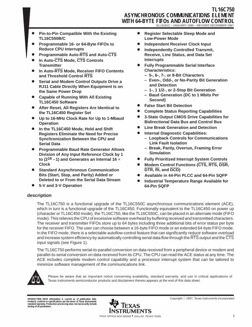
Two of the TL16C450 terminal functions have been changed to TXRDY and RXRDY, which provide signalingto a direct memory access (DMA) controller.
MROUT1DTRRTSOUT2NCINTRPTRXRDYA0A1A2
3938373635343332313029
18 19
7891011121314151617
D5D6D7
RCLKSINNC
SOUTCS0CS1CS2
BAUDOUT20 21 22 23
RI
DC
DD
SR
CT
S
5 4 3 2 16 44
D4
D3
D2
D1
D0
NC
VR
D2
DD
IST
XR
DY
AD
S
XIN
XO
UT
WR
1W
R2
NC
RD
1
42 41 4043
24 25 26 27 28
NC–No internal connection
CC
VS
S
FN PACKAGE(TOP VIEW)
18 19
D4NCD3D2NCD1D0NCVCCNCRINCDCDDSRNCCTS
48
47
46
45
44
43
42
41
40
39
38
37
36
35
34
3320
1
2
3
4
5
6
7
8
9
10
11
12
13
14
15
16
XINXOUT
NCWR1
NCWR2
NCVSSRD1RD2NC
DDISTXRDY
NCADS
NC21 22 23 24
PM PACKAGE(TOP VIEW)
D6
SIN
63 62 61 60 5964 58
CS
2
NC
CS
1N
CC
S0
SO
UT
NC
RT
SN
CD
TR
NC
NC A0
RX
RD
YN
CIN
TR
PT
NC
OU
T2
56 55 5457
25 26 27 28 29
53 52
17
A2
RC
LKN
C
51 50 49
30 31 32
OU
T1
NC
MR
D7
NC
D5
BA
UD
OU
TN
CA
1
TL16C750ASYNCHRONOUS COMMUNICATIONS ELEMENT
WITH 64-BYTE FIFOs AND AUTOFLOW CONTROLSLLS191C – JANUARY 1995 – REVISED DECEMBER 1997
3POST OFFICE BOX 655303 • DALLAS, TEXAS 75265
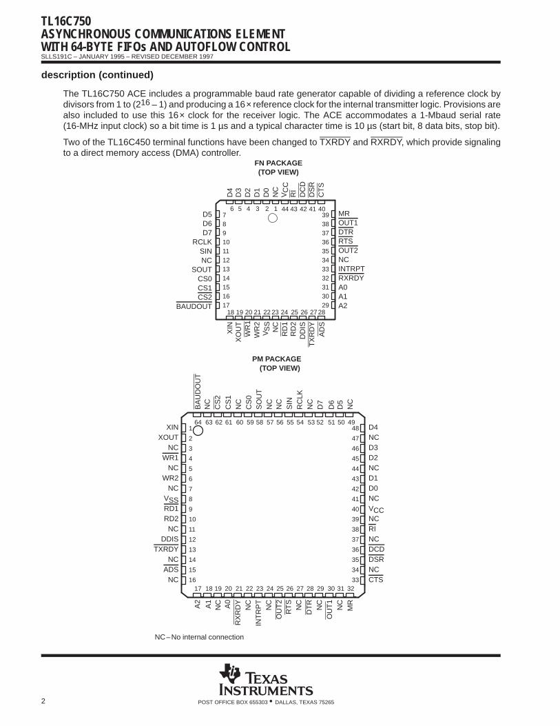
functional block diagram
ReceiverBuffer
Register
DivisorLatch (LS)
DivisorLatch (MS)
BaudGenerator
ReceiverFIFO
Line Status
Register
TransmitterHoldingRegister
Modem ControlRegister
Modem Status
Register
Line ControlRegister
TransmitterFIFO
Interrupt Enable
Register
Interrupt Identification
Register
FIFO ControlRegister
Selectand
ControlLogic
Interrupt ControlLogic
Select
Data Bus
Buffer
BAUDOUT
SIN
RCLK
SOUT
CTS
DTR
DSR
DCD
RI
OUT1
OUT2
INTRPT
40
37
41
42
43
38
35
33
13
10
11
17
14
A031
D(7–0)9–2
InternalData Bus
30
29
15
16
28
39
24
25
20
21
26
27
18
19
32
A1
A2
CS0
CS1
CS2
ADS
MR
RD1
RD2
WR1
WR2
DDIS
TXRDY
XIN
XOUT
RXRDY
Select
ReceiverShift
Register
ReceiverTiming and
Control
TransmitterTiming and
Control
TransmitterShift
Register
Modem ControlLogic
8
44
22VCC
VSSPowerSupply
RTS36
AutoflowControlEnable(AFE)
8
8
8
8
8
8 8
NOTE A: Terminal numbers shown are for the FN package.
TL16C750ASYNCHRONOUS COMMUNICATIONS ELEMENTWITH 64-BYTE FIFOs AND AUTOFLOW CONTROLSLLS191C – JANUARY 1995 – REVISED DECEMBER 1997
4 POST OFFICE BOX 655303 • DALLAS, TEXAS 75265
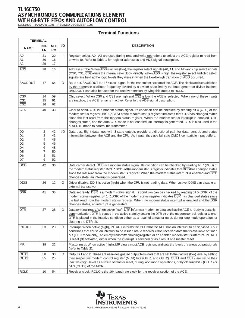
Terminal Functions
TERMINAL
NAMENO.FN
NO.PM
I/O DESCRIPTION
A0A1A2
313029
201817
I Register select. A0–A2 are used during read and write operations to select the ACE register to read fromor write to. Refer to Table 1 for register addresses and ADS signal description.
ADS 28 15 I Address strobe. When ADS is active (low), the register select signals (A0, A1, and A2) and chip select signals(CS0, CS1, CS2) drive the internal select logic directly; when ADS is high, the register select and chip selectsignals are held at the logic levels they were in when the low-to-high transition of ADS occurred.
BAUDOUT 17 64 O Baud out. BAUDOUT is a 16× clock signal for the transmitter section of the ACE. The clock rate is establishedby the reference oscillator frequency divided by a divisor specified by the baud generator divisor latches.BAUDOUT can also be used for the receiver section by tying this output to RCLK.
CS0CS1CS2
141516
596162
I Chip select. When CS0 and CS1 are high and CS2 is low, the ACE is selected. When any of these inputsare inactive, the ACE remains inactive. Refer to the ADS signal description.
CTS 40 33 I Clear to send. CTS is a modem status signal. Its condition can be checked by reading bit 4 (CTS) of themodem status register. Bit 0 (∆CTS) of the modem status register indicates that CTS has changed statessince the last read from the modem status register. When the modem status interrupt is enabled, CTSchanges states, and the auto-CTS mode is not enabled, an interrupt is generated. CTS is also used in theauto-CTS mode to control the transmitter.
D0D1D2D3D4D5D6D7
23456789
4243454648505152
I/O Data bus. Eight data lines with 3-state outputs provide a bidirectional path for data, control, and statusinformation between the ACE and the CPU. As inputs, they use fail safe CMOS compatible input buffers.
DCD 42 36 I Data carrier detect. DCD is a modem status signal. Its condition can be checked by reading bit 7 (DCD) ofthe modem status register. Bit 3 (∆DCD) of the modem status register indicates that DCD has changed statessince the last read from the modem status register. When the modem status interrupt is enabled and DCDchanges state, an interrupt is generated.
DDIS 26 12 O Driver disable. DDIS is active (high) when the CPU is not reading data. When active, DDIS can disable anexternal transceiver.
DSR 41 35 I Data set ready. DSR is a modem status signal. Its condition can be checked by reading bit 5 (DSR) of themodem status register. Bit 1 (∆DSR) of the modem status register indicates DSR has changed states sincethe last read from the modem status register. When the modem status interrupt is enabled and the DSRchanges states, an interrupt is generated.
DTR 37 28 O Data terminal ready. When active (low), DTR informs a modem or data set that the ACE is ready to establishcommunication. DTR is placed in the active state by setting the DTR bit of the modem control register to one.DTR is placed in the inactive condition either as a result of a master reset, during loop mode operation, orclearing the DTR bit.
INTRPT 33 23 O Interrupt. When active (high), INTRPT informs the CPU that the ACE has an interrupt to be serviced. Fourconditions that cause an interrupt to be issued are: a receiver error, received data that is available or timedout (FIFO mode only), an empty transmitter holding register, or an enabled modem status interrupt. INTRPTis reset (deactivated) either when the interrupt is serviced or as a result of a master reset.
MR 39 32 I Master reset. When active (high), MR clears most ACE registers and sets the levels of various output signals(refer to Table 2).
OUT1OUT2
3835
3025
O Outputs 1 and 2. These are user-designated output terminals that are set to their active (low) level by settingtheir respective modem control register (MCR) bits (OUT1 and OUT2). OUT1 and OUT2 are set to theirinactive (high) level as a result of master reset, during loop mode operations, or by clearing bit 2 (OUT1) orbit 3 (OUT2) of the MCR.
RCLK 10 54 I Receiver clock. RCLK is the 16× baud rate clock for the receiver section of the ACE.
TL16C750ASYNCHRONOUS COMMUNICATIONS ELEMENT
WITH 64-BYTE FIFOs AND AUTOFLOW CONTROLSLLS191C – JANUARY 1995 – REVISED DECEMBER 1997
5POST OFFICE BOX 655303 • DALLAS, TEXAS 75265
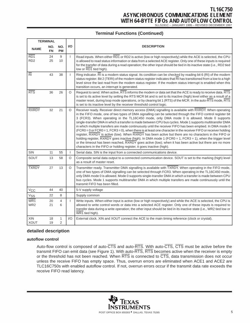
Terminal Functions (Continued)
TERMINAL
NAMENO.FN
NO.PM
I/O DESCRIPTION
RD1RD2
2425
910
I Read inputs. When either RD1 or RD2 is active (low or high respectively) while the ACE is selected, the CPUis allowed to read status information or data from a selected ACE register. Only one of these inputs is requiredfor the transfer of data during a read operation; the other input should be tied in its inactive state (i.e., RD2 tiedlow or RD1 tied high).
RI 43 38 I Ring indicator. RI is a modem status signal. Its condition can be checked by reading bit 6 (RI) of the modemstatus register. Bit 2 (TERI) of the modem status register indicates that RI has transitioned from a low to a highlevel since the last read from the modem status register. If the modem status interrupt is enabled when thistransition occurs, an interrupt is generated.
RTS 36 26 O Request to send. When active, RTS informs the modem or data set that the ACE is ready to receive data. RTSis set to its active level by setting the RTS MCR bit and is set to its inactive (high) level either as a result of amaster reset, during loop mode operations, or by clearing bit 1 (RTS) of the MCR. In the auto-RTS mode, RTSis set to its inactive level by the receiver threshold control logic.
RXRDY 32 21 O Receiver ready. Receiver direct memory access (DMA) signalling is available with RXRDY. When operatingin the FIFO mode, one of two types of DMA signalling can be selected through the FIFO control register bit3 (FCR3). When operating in the TL16C450 mode, only DMA mode 0 is allowed. Mode 0 supportssingle-transfer DMA in which a transfer is made between CPU bus cycles. Mode 1 supports multitransfer DMAin which multiple transfers are made continuously until the receiver FIFO has been emptied. In DMA mode 0(FCR0 = 0 or FCR0 = 1, FCR3 = 0), when there is at least one character in the receiver FIFO or receiver holdingregister, RXRDY is active (low). When RXRDY has been active but there are no characters in the FIFO orholding register, RXRDY goes inactive (high). In DMA mode 1 (FCR0 = 1, FCR3 = 1), when the trigger levelor the timeout has been reached, RXRDY goes active (low); when it has been active but there are no morecharacters in the FIFO or holding register, it goes inactive (high).
SIN 11 55 I Serial data. SIN is the input from a connected communications device.
SOUT 13 58 O Composite serial data output to a connected communication device. SOUT is set to the marking (high) levelas a result of master reset.
TXRDY 27 13 O Transmitter ready. Transmitter DMA signalling is available with TXRDY. When operating in the FIFO mode,one of two types of DMA signalling can be selected through FCR3. When operating in the TL16C450 mode,only DMA mode 0 is allowed. Mode 0 supports single-transfer DMA in which a transfer is made between CPUbus cycles. Mode 1 supports multitransfer DMA in which multiple transfers are made continuously until thetransmit FIFO has been filled.
VCC 44 40 5-V supply voltage
VSS 22 8 Supply common
WR1WR2
2021
46
I Write inputs. When either input is active (low or high respectively) and while the ACE is selected, the CPU isallowed to write control words or data into a selected ACE register. Only one of these inputs is required totransfer data during a write operation; the other input should be tied in its inactive state (i.e., WR2 tied low orWR1 tied high).
XINXOUT
1819
12
I/O External clock. XIN and XOUT connect the ACE to the main timing reference (clock or crystal).
detailed description
autoflow control
Auto-flow control is composed of auto-CTS and auto-RTS. With auto-CTS, CTS must be active before thetransmit FIFO can emit data (see Figure 1). With auto-RTS, RTS becomes active when the receiver is emptyor the threshold has not been reached. When RTS is connected to CTS, data transmission does not occurunless the receive FIFO has empty space. Thus, overrun errors are eliminated when ACE1 and ACE2 areTLC16C750s with enabled autoflow control. If not, overrun errors occur if the transmit data rate exceeds thereceive FIFO read latency.
TL16C750ASYNCHRONOUS COMMUNICATIONS ELEMENTWITH 64-BYTE FIFOs AND AUTOFLOW CONTROLSLLS191C – JANUARY 1995 – REVISED DECEMBER 1997
6 POST OFFICE BOX 655303 • DALLAS, TEXAS 75265
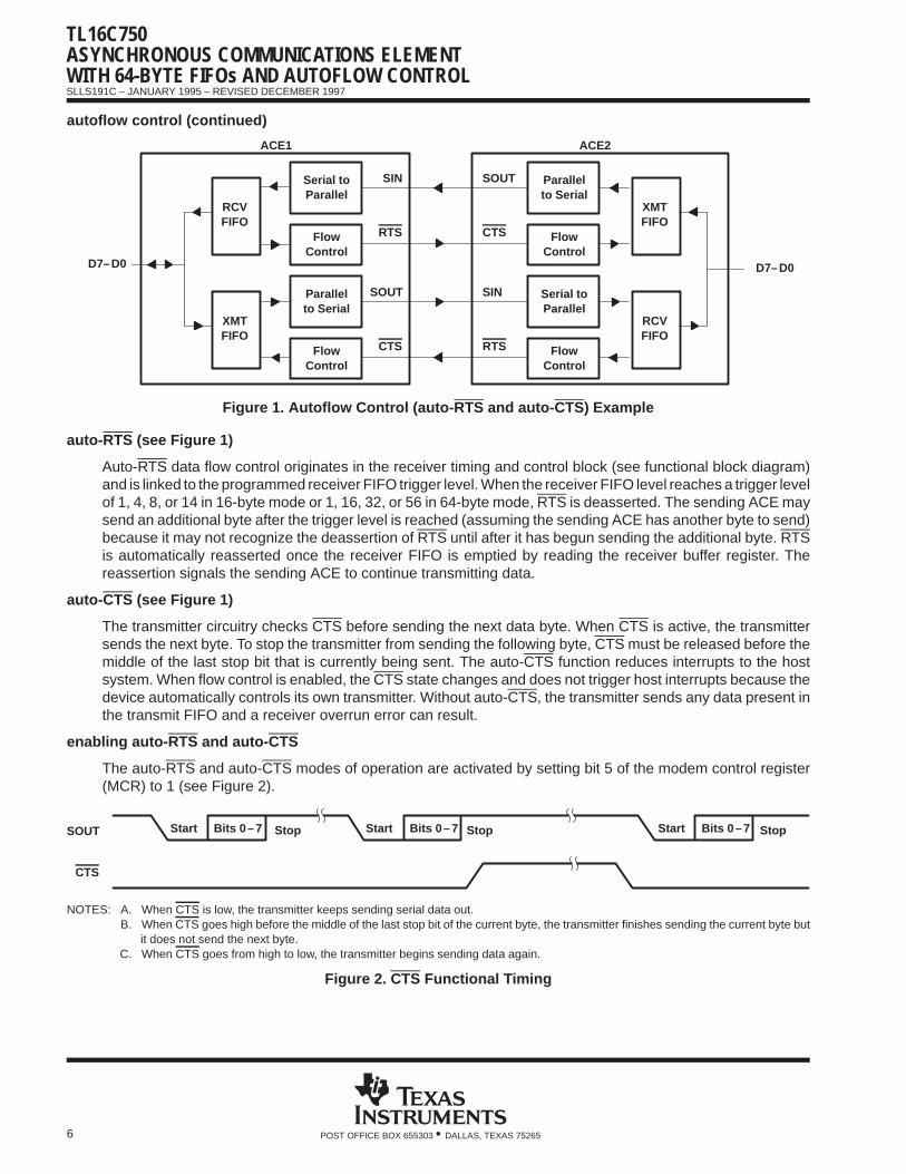
autoflow control (continued)
Serial toParallel
FlowControl
Parallelto Serial
FlowControl
Parallelto Serial
FlowControl
Serial toParallel
FlowControl
XMTFIFO
RCVFIFO
ACE1 ACE2
D7–D0D7–D0
SIN SOUT
RTS CTS
SOUT SIN
CTS RTS
XMTFIFO
RCVFIFO
Figure 1. Autoflow Control (auto-RTS and auto-CTS ) Example
auto-RTS (see Figure 1)
Auto-RTS data flow control originates in the receiver timing and control block (see functional block diagram)and is linked to the programmed receiver FIFO trigger level. When the receiver FIFO level reaches a trigger levelof 1, 4, 8, or 14 in 16-byte mode or 1, 16, 32, or 56 in 64-byte mode, RTS is deasserted. The sending ACE maysend an additional byte after the trigger level is reached (assuming the sending ACE has another byte to send)because it may not recognize the deassertion of RTS until after it has begun sending the additional byte. RTSis automatically reasserted once the receiver FIFO is emptied by reading the receiver buffer register. Thereassertion signals the sending ACE to continue transmitting data.
auto-CTS (see Figure 1)
The transmitter circuitry checks CTS before sending the next data byte. When CTS is active, the transmittersends the next byte. To stop the transmitter from sending the following byte, CTS must be released before themiddle of the last stop bit that is currently being sent. The auto-CTS function reduces interrupts to the hostsystem. When flow control is enabled, the CTS state changes and does not trigger host interrupts because thedevice automatically controls its own transmitter. Without auto-CTS, the transmitter sends any data present inthe transmit FIFO and a receiver overrun error can result.
enabling auto-RTS and auto-CTS
The auto-RTS and auto-CTS modes of operation are activated by setting bit 5 of the modem control register(MCR) to 1 (see Figure 2).
Start Bits 0–7 Start Bits 0–7 Start Bits 0–7Stop Stop StopSOUT
CTS
NOTES: A. When CTS is low, the transmitter keeps sending serial data out.B. When CTS goes high before the middle of the last stop bit of the current byte, the transmitter finishes sending the current byte but
it does not send the next byte.C. When CTS goes from high to low, the transmitter begins sending data again.
Figure 2. CTS Functional Timing
TL16C750ASYNCHRONOUS COMMUNICATIONS ELEMENT
WITH 64-BYTE FIFOs AND AUTOFLOW CONTROLSLLS191C – JANUARY 1995 – REVISED DECEMBER 1997
7POST OFFICE BOX 655303 • DALLAS, TEXAS 75265
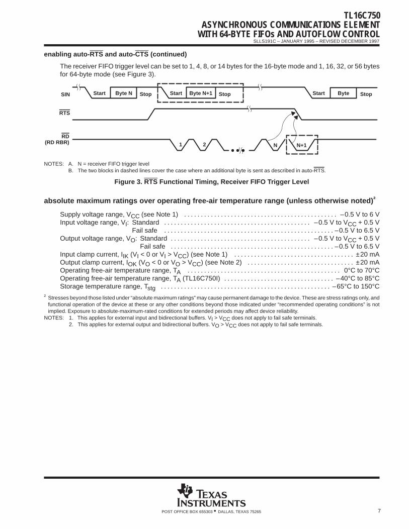
enabling auto-RTS and auto-CTS (continued)
The receiver FIFO trigger level can be set to 1, 4, 8, or 14 bytes for the 16-byte mode and 1, 16, 32, or 56 bytesfor 64-byte mode (see Figure 3).
Start Byte N Start Byte N+1 Start ByteStop Stop StopSIN
RTS
RD(RD RBR) 1 2 N N+1
NOTES: A. N = receiver FIFO trigger levelB. The two blocks in dashed lines cover the case where an additional byte is sent as described in auto-RTS.
Figure 3. RTS Functional Timing, Receiver FIFO Trigger Level
absolute maximum ratings over operating free-air temperature range (unless otherwise noted) †
Supply voltage range, VCC (see Note 1) –0.5 V to 6 V. . . . . . . . . . . . . . . . . . . . . . . . . . . . . . . . . . . . . . . . . . . . . . Input voltage range, VI: Standard –0.5 V to VCC + 0.5 V. . . . . . . . . . . . . . . . . . . . . . . . . . . . . . . . . . . . . . . . . . . .
Fail safe –0.5 V to 6.5 V. . . . . . . . . . . . . . . . . . . . . . . . . . . . . . . . . . . . . . . . . . . . . . . . . . . Output voltage range, VO: Standard –0.5 V to VCC + 0.5 V. . . . . . . . . . . . . . . . . . . . . . . . . . . . . . . . . . . . . . . . . .
Fail safe –0.5 V to 6.5 V. . . . . . . . . . . . . . . . . . . . . . . . . . . . . . . . . . . . . . . . . . . . . . . . . Input clamp current, IIK (VI < 0 or VI > VCC) (see Note 1) ±20 mA. . . . . . . . . . . . . . . . . . . . . . . . . . . . . . . . . . . . Output clamp current, IOK (VO < 0 or VO > VCC) (see Note 2) ±20 mA. . . . . . . . . . . . . . . . . . . . . . . . . . . . . . . . Operating free-air temperature range, TA 0°C to 70°C. . . . . . . . . . . . . . . . . . . . . . . . . . . . . . . . . . . . . . . . . . . . . . Operating free-air temperature range, TA (TL16C750I) –40°C to 85°C. . . . . . . . . . . . . . . . . . . . . . . . . . . . . . . . . Storage temperature range, Tstg –65°C to 150°C. . . . . . . . . . . . . . . . . . . . . . . . . . . . . . . . . . . . . . . . . . . . . . . . . . .
† Stresses beyond those listed under “absolute maximum ratings” may cause permanent damage to the device. These are stress ratings only, andfunctional operation of the device at these or any other conditions beyond those indicated under “recommended operating conditions” is notimplied. Exposure to absolute-maximum-rated conditions for extended periods may affect device reliability.
NOTES: 1. This applies for external input and bidirectional buffers. VI > VCC does not apply to fail safe terminals.2. This applies for external output and bidirectional buffers. VO > VCC does not apply to fail safe terminals.
TL16C750ASYNCHRONOUS COMMUNICATIONS ELEMENTWITH 64-BYTE FIFOs AND AUTOFLOW CONTROLSLLS191C – JANUARY 1995 – REVISED DECEMBER 1997
8 POST OFFICE BOX 655303 • DALLAS, TEXAS 75265
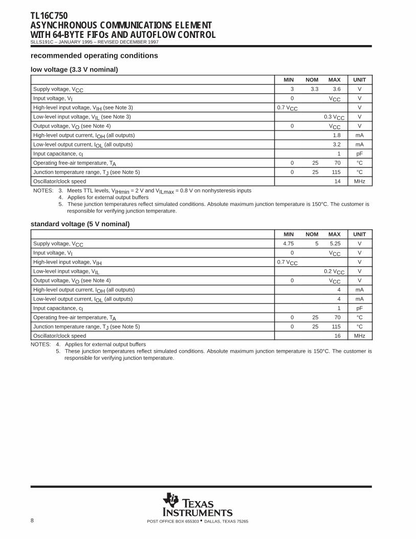
recommended operating conditions
low voltage (3.3 V nominal)MIN NOM MAX UNIT
Supply voltage, VCC 3 3.3 3.6 V
Input voltage, VI 0 VCC V
High-level input voltage, VIH (see Note 3) 0.7 VCC V
Low-level input voltage, VIL (see Note 3) 0.3 VCC V
Output voltage, VO (see Note 4) 0 VCC V
High-level output current, IOH (all outputs) 1.8 mA
Low-level output current, IOL (all outputs) 3.2 mA
Input capacitance, cI 1 pF
Operating free-air temperature, TA 0 25 70 °C
Junction temperature range, TJ (see Note 5) 0 25 115 °C
Oscillator/clock speed 14 MHz
NOTES: 3. Meets TTL levels, VIHmin = 2 V and VILmax = 0.8 V on nonhysteresis inputs4. Applies for external output buffers5. These junction temperatures reflect simulated conditions. Absolute maximum junction temperature is 150°C. The customer is
responsible for verifying junction temperature.
standard voltage (5 V nominal)MIN NOM MAX UNIT
Supply voltage, VCC 4.75 5 5.25 V
Input voltage, VI 0 VCC V
High-level input voltage, VIH 0.7 VCC V
Low-level input voltage, VIL 0.2 VCC V
Output voltage, VO (see Note 4) 0 VCC V
High-level output current, IOH (all outputs) 4 mA
Low-level output current, IOL (all outputs) 4 mA
Input capacitance, cI 1 pF
Operating free-air temperature, TA 0 25 70 °C
Junction temperature range, TJ (see Note 5) 0 25 115 °C
Oscillator/clock speed 16 MHz
NOTES: 4. Applies for external output buffers5. These junction temperatures reflect simulated conditions. Absolute maximum junction temperature is 150°C. The customer is
responsible for verifying junction temperature.
TL16C750ASYNCHRONOUS COMMUNICATIONS ELEMENT
WITH 64-BYTE FIFOs AND AUTOFLOW CONTROLSLLS191C – JANUARY 1995 – REVISED DECEMBER 1997
9POST OFFICE BOX 655303 • DALLAS, TEXAS 75265
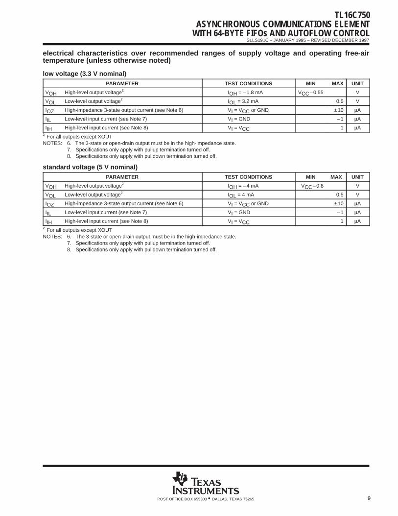
electrical characteristics over recommended ranges of supply voltage and operating free-airtemperature (unless otherwise noted)
low voltage (3.3 V nominal)PARAMETER TEST CONDITIONS MIN MAX UNIT
VOH High-level output voltage† IOH = –1.8 mA VCC–0.55 V
VOL Low-level output voltage† IOL = 3.2 mA 0.5 V
IOZ High-impedance 3-state output current (see Note 6) VI = VCC or GND ±10 µA
IIL Low-level input current (see Note 7) VI = GND –1 µA
IIH High-level input current (see Note 8) VI = VCC 1 µA
† For all outputs except XOUTNOTES: 6. The 3-state or open-drain output must be in the high-impedance state.
7. Specifications only apply with pullup termination turned off.8. Specifications only apply with pulldown termination turned off.
standard voltage (5 V nominal)PARAMETER TEST CONDITIONS MIN MAX UNIT
VOH High-level output voltage† IOH = –4 mA VCC–0.8 V
VOL Low-level output voltage† IOL = 4 mA 0.5 V
IOZ High-impedance 3-state output current (see Note 6) VI = VCC or GND ±10 µA
IIL Low-level input current (see Note 7) VI = GND –1 µA
IIH High-level input current (see Note 8) VI = VCC 1 µA
† For all outputs except XOUTNOTES: 6. The 3-state or open-drain output must be in the high-impedance state.
7. Specifications only apply with pullup termination turned off.8. Specifications only apply with pulldown termination turned off.
TL16C750ASYNCHRONOUS COMMUNICATIONS ELEMENTWITH 64-BYTE FIFOs AND AUTOFLOW CONTROLSLLS191C – JANUARY 1995 – REVISED DECEMBER 1997
10 POST OFFICE BOX 655303 • DALLAS, TEXAS 75265
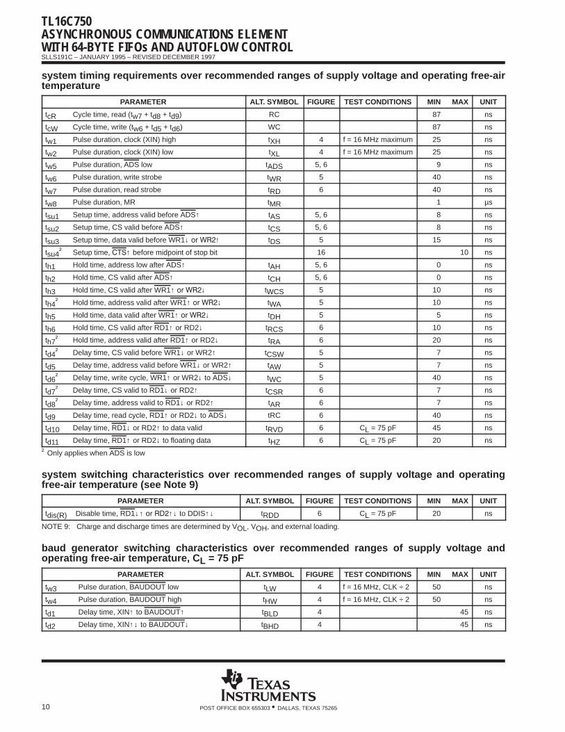
system timing requirements over recommended ranges of supply voltage and operating free-airtemperature
PARAMETER ALT. SYMBOL FIGURE TEST CONDITIONS MIN MAX UNIT
tcR Cycle time, read (tw7 + td8 + td9) RC 87 ns
tcW Cycle time, write (tw6 + td5 + td6) WC 87 ns
tw1 Pulse duration, clock (XIN) high tXH 4 f = 16 MHz maximum 25 ns
tw2 Pulse duration, clock (XIN) low tXL 4 f = 16 MHz maximum 25 ns
tw5 Pulse duration, ADS low tADS 5, 6 9 ns
tw6 Pulse duration, write strobe tWR 5 40 ns
tw7 Pulse duration, read strobe tRD 6 40 ns
tw8 Pulse duration, MR tMR 1 µs
tsu1 Setup time, address valid before ADS↑ tAS 5, 6 8 ns
tsu2 Setup time, CS valid before ADS↑ tCS 5, 6 8 ns
tsu3 Setup time, data valid before WR1↓ ↑ tDS 5 15 ns
tsu4† Setup time, ↑ before midpoint of stop bit 16 10 ns
th1 Hold time, address low after ADS↑ tAH 5, 6 0 ns
th2 Hold time, CS valid after ADS↑ tCH 5, 6 0 ns
th3 Hold time, CS valid after WR1↑ ↓ tWCS 5 10 ns
th4† Hold time, address valid after WR1↑ ↓ tWA 5 10 ns
th5 Hold time, data valid after WR1↑ ↓ tDH 5 5 ns
th6 Hold time, CS valid after RD1↑ or RD2↓ tRCS 6 10 ns
th7† Hold time, address valid after RD1↑ or RD2↓ tRA 6 20 ns
td4† Delay time, CS valid before WR1↓ or WR2↑ tCSW 5 7 ns
td5 Delay time, address valid before WR1↓ or WR2↑ tAW 5 7 ns
td6† Delay time, write cycle, WR1↑ or WR2↓ to ADS↓ tWC 5 40 ns
td7† Delay time, CS valid to RD1↓ or RD2↑ tCSR 6 7 ns
td8† Delay time, address valid to RD1↓ or RD2↑ tAR 6 7 ns
td9 Delay time, read cycle, RD1↑ or RD2↓ to ADS↓ tRC 6 40 ns
td10 Delay time, RD1↓ or RD2↑ to data valid tRVD 6 CL = 75 pF 45 ns
td11 Delay time, RD1↑ or RD2↓ to floating data tHZ 6 CL = 75 pF 20 ns
† Only applies when ADS is low
system switching characteristics over recommended ranges of supply voltage and operatingfree-air temperature (see Note 9)
PARAMETER ALT. SYMBOL FIGURE TEST CONDITIONS MIN MAX UNIT
tdis(R) Disable time, RD1↓↑ ↑↓ to DDIS↑↓ tRDD 6 CL = 75 pF 20 ns
NOTE 9: Charge and discharge times are determined by VOL, VOH, and external loading.
baud generator switching characteristics over recommended ranges of supply voltage andoperating free-air temperature, C L = 75 pF
PARAMETER ALT. SYMBOL FIGURE TEST CONDITIONS MIN MAX UNIT
tw3 Pulse duration, BAUDOUT low tLW 4 f = 16 MHz, CLK ÷ 2 50 ns
tw4 Pulse duration, BAUDOUT high tHW 4 f = 16 MHz, CLK ÷ 2 50 ns
td1 Delay time, XIN↑ to BAUDOUT↑ tBLD 4 45 ns
td2 Delay time, XIN↑↓ to BAUDOUT↓ tBHD 4 45 ns
TL16C750ASYNCHRONOUS COMMUNICATIONS ELEMENT
WITH 64-BYTE FIFOs AND AUTOFLOW CONTROLSLLS191C – JANUARY 1995 – REVISED DECEMBER 1997
11POST OFFICE BOX 655303 • DALLAS, TEXAS 75265
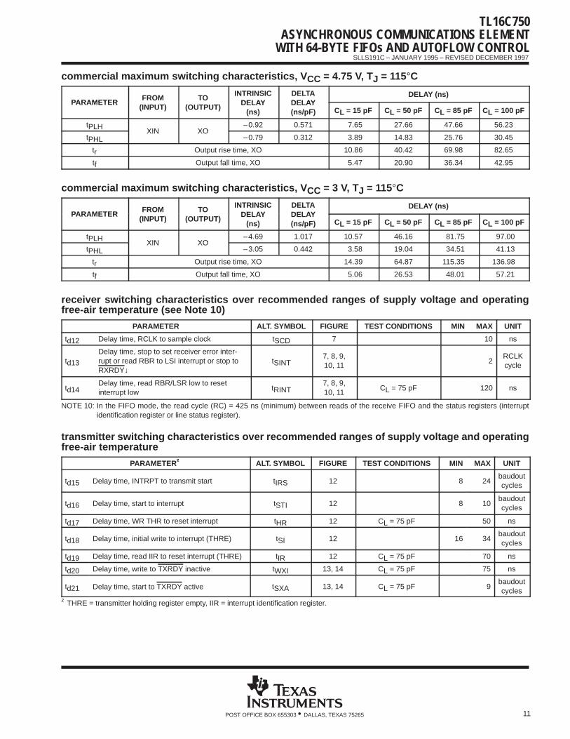
commercial maximum switching characteristics, V CC = 4.75 V, TJ = 115°C
PARAMETERFROM TO
INTRINSICDELAY
DELTADELAY
DELAY (ns)PARAMETER
(INPUT) (OUTPUT)DELAY
(ns)DELAY(ns/pF) CL = 15 pF CL = 50 pF CL = 85 pF CL = 100 pF
tPLHXIN XO
–0.92 0.571 7.65 27.66 47.66 56.23
tPHLXIN XO
–0.79 0.312 3.89 14.83 25.76 30.45
tr Output rise time, XO 10.86 40.42 69.98 82.65
tf Output fall time, XO 5.47 20.90 36.34 42.95
commercial maximum switching characteristics, V CC = 3 V, TJ = 115°C
PARAMETERFROM TO
INTRINSICDELAY
DELTADELAY
DELAY (ns)PARAMETER
(INPUT) (OUTPUT)DELAY
(ns)DELAY(ns/pF) CL = 15 pF CL = 50 pF CL = 85 pF CL = 100 pF
tPLHXIN XO
–4.69 1.017 10.57 46.16 81.75 97.00
tPHLXIN XO
–3.05 0.442 3.58 19.04 34.51 41.13
tr Output rise time, XO 14.39 64.87 115.35 136.98
tf Output fall time, XO 5.06 26.53 48.01 57.21
receiver switching characteristics over recommended ranges of supply voltage and operatingfree-air temperature (see Note 10)
PARAMETER ALT. SYMBOL FIGURE TEST CONDITIONS MIN MAX UNIT
td12 Delay time, RCLK to sample clock tSCD 7 10 ns
td13
Delay time, stop to set receiver error inter-rupt or read RBR to LSI interrupt or stop to RXRDY↓
tSINT7, 8, 9,10, 11
2RCLKcycle
td14Delay time, read RBR/LSR low to reset interrupt low
tRINT7, 8, 9,10, 11
CL = 75 pF 120 ns
NOTE 10: In the FIFO mode, the read cycle (RC) = 425 ns (minimum) between reads of the receive FIFO and the status registers (interruptidentification register or line status register).
transmitter switching characteristics over recommended ranges of supply voltage and operatingfree-air temperature
PARAMETER† ALT. SYMBOL FIGURE TEST CONDITIONS MIN MAX UNIT
td15 Delay time, INTRPT to transmit start tIRS 12 8 24baudoutcycles
td16 Delay time, start to interrupt tSTI 12 8 10baudoutcycles
td17 Delay time, WR THR to reset interrupt tHR 12 CL = 75 pF 50 ns
td18 Delay time, initial write to interrupt (THRE) tSI 12 16 34baudoutcycles
td19 Delay time, read IIR to reset interrupt (THRE) tIR 12 CL = 75 pF 70 ns
td20 Delay time, write to TXRDY inactive tWXI 13, 14 CL = 75 pF 75 ns
td21 Delay time, start to TXRDY active tSXA 13, 14 CL = 75 pF 9baudoutcycles
† THRE = transmitter holding register empty, IIR = interrupt identification register.
TL16C750ASYNCHRONOUS COMMUNICATIONS ELEMENTWITH 64-BYTE FIFOs AND AUTOFLOW CONTROLSLLS191C – JANUARY 1995 – REVISED DECEMBER 1997
12 POST OFFICE BOX 655303 • DALLAS, TEXAS 75265
modem control switching characteristics over recommended ranges of supply voltage andoperating free-air temperature, C L = 75 pF
PARAMETER ALT. SYMBOL FIGURE MIN MAX UNIT
td22 Delay time, WR MCR to output tMDO 15 60 ns
td23 Delay time, modem interrupt to set interrupt tSIM 15 35 ns
td24 Delay time, RD MSR to reset interrupt tRIM 15 45 ns
td25 Delay time, CTS low to SOUT↓ 16 24 baudoutcycles
td26 Delay time, receiver threshold byte to RTS↑ 17 2 baudoutcycles
td27 Delay time, read of last byte in receive FIFO to RTS↓ 17 3 baudoutcycles
PARAMETER MEASUREMENT INFORMATION
BAUDOUT(1/1)
XIN
BAUDOUT(1/2)
BAUDOUT(1/3)
BAUDOUT(1/N)
(N > 3)2 XIN Cycles
(N–2) XIN Cycles
tw3tw4
td1td2
td1td2
N
tw1 tw2
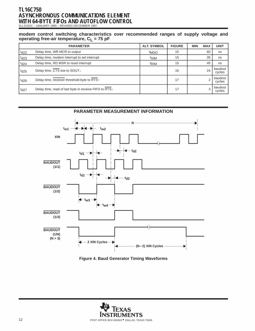
Figure 4. Baud Generator Timing Waveforms
TL16C750ASYNCHRONOUS COMMUNICATIONS ELEMENT
WITH 64-BYTE FIFOs AND AUTOFLOW CONTROLSLLS191C – JANUARY 1995 – REVISED DECEMBER 1997
13POST OFFICE BOX 655303 • DALLAS, TEXAS 75265
PARAMETER MEASUREMENT INFORMATION
ADS
tw5
th1
tsu1
th2
tsu2
tsu3th5
th3tw6td4
td5 td6
th4†
Valid Data
Valid Valid †
Valid Valid †
Active
A0–A2
CS0, CS1, CS2
WR1, WR2
D7–D0
50%50%
50% 50%50%
50% 50%
50% 50%
50%
† Applicable only when ADS is low
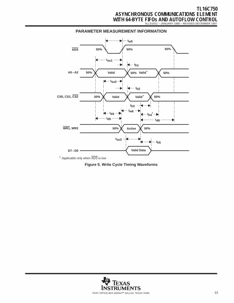
Figure 5. Write Cycle Timing Waveforms
TL16C750ASYNCHRONOUS COMMUNICATIONS ELEMENTWITH 64-BYTE FIFOs AND AUTOFLOW CONTROLSLLS191C – JANUARY 1995 – REVISED DECEMBER 1997
14 POST OFFICE BOX 655303 • DALLAS, TEXAS 75265
PARAMETER MEASUREMENT INFORMATION
ADS
tw5
th1
tsu1
th2
tsu2
td10td11
th6tw7
td7†
td8† td9
th7†
Valid Data
Valid Valid †
Valid Valid †
Active
A0–A2
CS0, CS1, CS2
RD1, RD2
D7–D0
tdis(R)tdis(R)
DDIS
50%50% 50%
50%
50%
50% 50%
50% 50%
50% 50%
50% 50%
† Applicable only when ADS is low
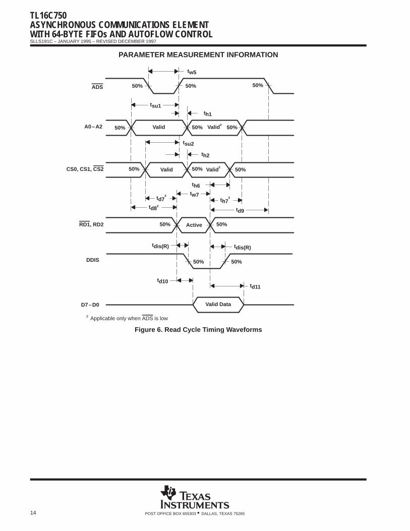
Figure 6. Read Cycle Timing Waveforms
TL16C750ASYNCHRONOUS COMMUNICATIONS ELEMENT
WITH 64-BYTE FIFOs AND AUTOFLOW CONTROLSLLS191C – JANUARY 1995 – REVISED DECEMBER 1997
15POST OFFICE BOX 655303 • DALLAS, TEXAS 75265
PARAMETER MEASUREMENT INFORMATION
td13
Active
Active
RD1, RD2(read RBR)
RCLK
td14
8 Clockstd12
Parity StopStart Data Bits 5–8
Sample Clock
TL16C450 Mode:
Sample Clock
SIN
INTRPT(data ready)
INTRPT(receiver error)
RD1, RD2(read LSR)
50%50%
50%
50% 50%
50%
td14
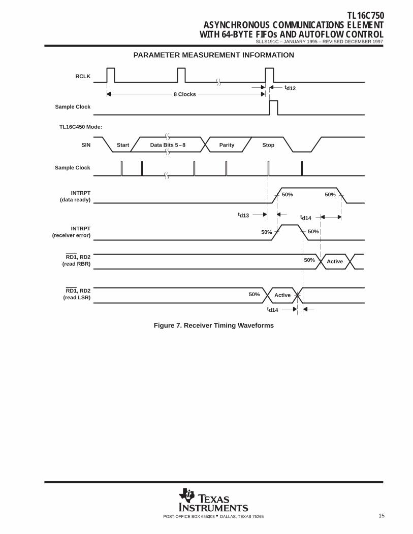
Figure 7. Receiver Timing Waveforms
TL16C750ASYNCHRONOUS COMMUNICATIONS ELEMENTWITH 64-BYTE FIFOs AND AUTOFLOW CONTROLSLLS191C – JANUARY 1995 – REVISED DECEMBER 1997
16 POST OFFICE BOX 655303 • DALLAS, TEXAS 75265
PARAMETER MEASUREMENT INFORMATION
td13(see Note A)
td14
StopData Bits 5–8
Sample Clock
SIN
Trigger LevelINTRPT
(FCR6, 7 = 0, 0)
Line StatusINTRPT
(LSI)td14
RD1(RD LSR)
RD1(RD RBR)
Active
Active
(FIFO at or abovetrigger level)
(FIFO belowtrigger level)
50%50%
50%
50%
50% 50%
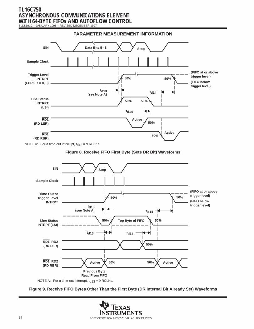
NOTE A: For a time-out interrupt, td13 = 9 RCLKs.
Figure 8. Receive FIFO First Byte (Sets DR Bit) Waveforms
td13(see Note A ) td14
Stop
Top Byte of FIFO
Sample Clock
SIN
Time-Out orTrigger Level
INTRPT
Line StatusINTRPT (LSI)
td13
(FIFO at or abovetrigger level)
(FIFO belowtrigger level)
RD1, RD2(RD LSR)
RD1, RD2(RD RBR)
Active Active
td14
Previous ByteRead From FIFO
50%50%
50%50%
50%
50% 50%
NOTE A: For a time-out interrupt, td13 = 9 RCLKs.
Figure 9. Receive FIFO Bytes Other Than the First Byte (DR Internal Bit Already Set) Waveforms
TL16C750ASYNCHRONOUS COMMUNICATIONS ELEMENT
WITH 64-BYTE FIFOs AND AUTOFLOW CONTROLSLLS191C – JANUARY 1995 – REVISED DECEMBER 1997
17POST OFFICE BOX 655303 • DALLAS, TEXAS 75265
PARAMETER MEASUREMENT INFORMATION
td13(see Note B) td14
Stop
Sample Clock
SIN(first byte)
ActiveRD
(RD RBR)
RXRDY
See Note A
50%
50%50%
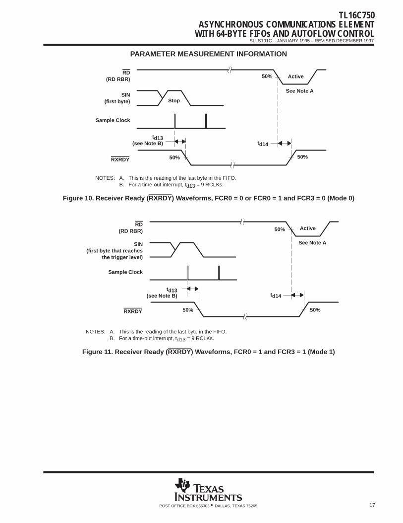
NOTES: A. This is the reading of the last byte in the FIFO.B. For a time-out interrupt, td13 = 9 RCLKs.
Figure 10. Receiver Ready (RXRDY ) Waveforms, FCR0 = 0 or FCR0 = 1 and FCR3 = 0 (Mode 0)
td13(see Note B) td14
Sample Clock
SIN(first byte that reaches
the trigger level)
ActiveRD
(RD RBR)
RXRDY
See Note A
50%
50%50%
NOTES: A. This is the reading of the last byte in the FIFO.B. For a time-out interrupt, td13 = 9 RCLKs.
Figure 11. Receiver Ready (RXRDY ) Waveforms, FCR0 = 1 and FCR3 = 1 (Mode 1)
TL16C750ASYNCHRONOUS COMMUNICATIONS ELEMENTWITH 64-BYTE FIFOs AND AUTOFLOW CONTROLSLLS191C – JANUARY 1995 – REVISED DECEMBER 1997
18 POST OFFICE BOX 655303 • DALLAS, TEXAS 75265
PARAMETER MEASUREMENT INFORMATION
td16
Parity StopStart
Data BitsSOUTStart
td15
td17td17
td18
td19
INTRPT(THRE)
WR THR
RD IIR
50% 50% 50% 50% 50%
50%50%50%
50%50%
50%
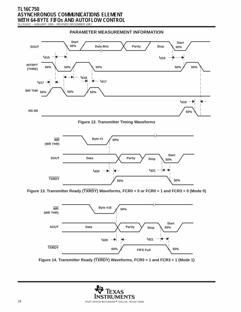
Figure 12. Transmitter Timing Waveforms
td20
WR(WR THR)
td21
Parity StopDataStart
Byte #1
SOUT
TXRDY
50%
50%
50%50%
Figure 13. Transmitter Ready (TXRDY ) Waveforms, FCR0 = 0 or FCR0 = 1 and FCR3 = 0 (Mode 0)
WR(WR THR)
Parity StopDataStart
Byte #16
SOUT
TXRDYFIFO Full
td20 td21
50%
50%
50%
50%
Figure 14. Transmitter Ready (TXRDY ) Waveforms, FCR0 = 1 and FCR3 = 1 (Mode 1)
TL16C750ASYNCHRONOUS COMMUNICATIONS ELEMENT
WITH 64-BYTE FIFOs AND AUTOFLOW CONTROLSLLS191C – JANUARY 1995 – REVISED DECEMBER 1997
19POST OFFICE BOX 655303 • DALLAS, TEXAS 75265
PARAMETER MEASUREMENT INFORMATION
td22 td22
WR(WR MCR)
RTS, DTR,OUT1, OUT2
CTS, DSR, DCD
td23
td24
td23
INTRPT(modem)
RD2(RD MSR)
RI
50% 50%
50% 50%
50%
50% 50%
50%
50%
50%
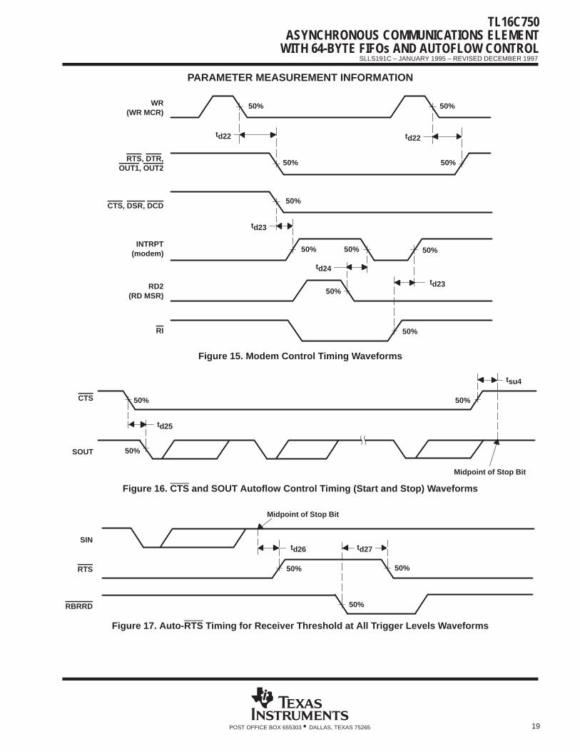
Figure 15. Modem Control Timing Waveforms
Midpoint of Stop Bit
td25
tsu4
CTS
SOUT
50% 50%
50%
Figure 16. CTS and SOUT Autoflow Control Timing (Start and Stop) Waveforms
td27SIN
50%
td26
50%
50%
Midpoint of Stop Bit
RTS
RBRRD
Figure 17. Auto-RTS Timing for Receiver Threshold at All Trigger Levels Waveforms
TL16C750ASYNCHRONOUS COMMUNICATIONS ELEMENTWITH 64-BYTE FIFOs AND AUTOFLOW CONTROLSLLS191C – JANUARY 1995 – REVISED DECEMBER 1997
20 POST OFFICE BOX 655303 • DALLAS, TEXAS 75265
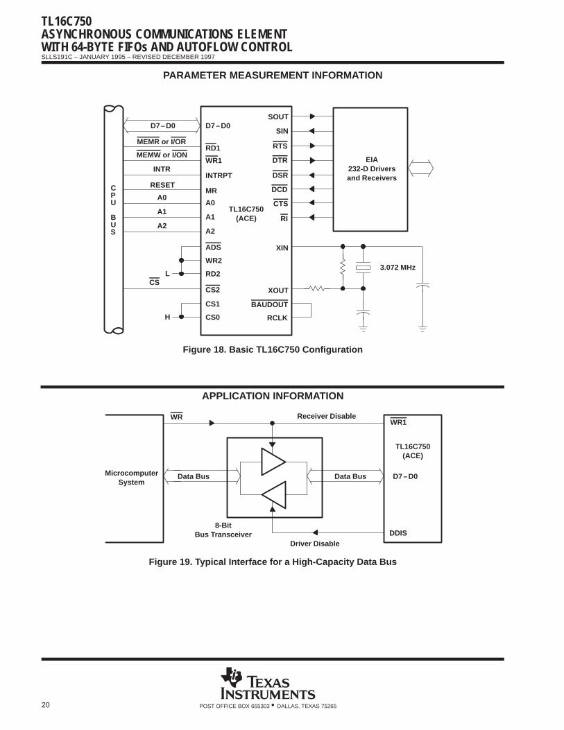
PARAMETER MEASUREMENT INFORMATION
D7–D0
MEMR or I/OR
MEMW or I/ON
INTR
RESET
A0
A1
A2
CSL
H
EIA232-D Driversand Receivers
XOUT
XIN
RCLK
BAUDOUT
RI
CTS
DCD
DSR
DTR
RTS
SOUT
SIN
INTRPT
D7–D0
RD1
WR1
MR
A0
A1
A2
ADS
WR2
RD2
CS2
CS1
CS0
TL16C750(ACE)
3.072 MHz
CPU
BUS
Figure 18. Basic TL16C750 Configuration
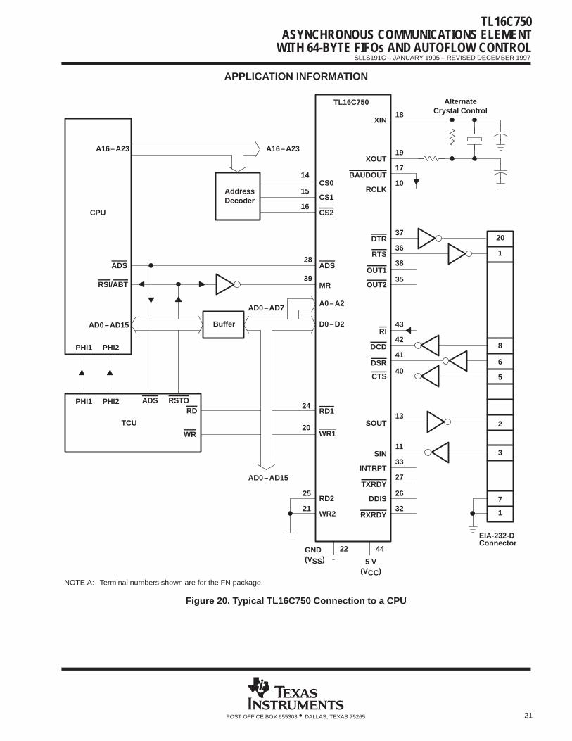
APPLICATION INFORMATION
Receiver Disable
MicrocomputerSystem
Data Bus Data Bus
Driver Disable
8-BitBus Transceiver
WRWR1
D7–D0
DDIS
TL16C750(ACE)
Figure 19. Typical Interface for a High-Capacity Data Bus
TL16C750ASYNCHRONOUS COMMUNICATIONS ELEMENT
WITH 64-BYTE FIFOs AND AUTOFLOW CONTROLSLLS191C – JANUARY 1995 – REVISED DECEMBER 1997
21POST OFFICE BOX 655303 • DALLAS, TEXAS 75265
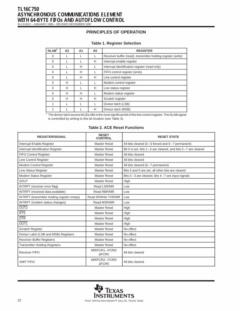
APPLICATION INFORMATION
Buffer
AddressDecoder
A16–A23
ADS
AD0–AD15
RSI/ABT
PHI1 PHI2
PHI1 PHI2 ADS
ADS
CPU
RSTO
A16–A23
CS0
CS1
CS2
MR
A0–A2
D0–D2
AD0–AD7
RD1
WR1
AD0–AD15
RD2
WR2
XIN
XOUT
BAUDOUT
RCLK
DTR
RTS
OUT1
OUT2
RI
DCD
DSR
CTS
SIN
SOUT
INTRPT
TXRDY
DDIS
RXRDY
GND(VSS) 5 V
(VCC)
22 44
AlternateCrystal Control
TL16C750
EIA-232-DConnector
20
1
8
6
5
2
3
7
1
18
19
17
10
37
36
38
35
43
42
41
40
11
33
27
26
13
3221
25
20
24
28
39
14
15
16
TCU
WR
RD
NOTE A: Terminal numbers shown are for the FN package.
Figure 20. Typical TL16C750 Connection to a CPU
TL16C750ASYNCHRONOUS COMMUNICATIONS ELEMENTWITH 64-BYTE FIFOs AND AUTOFLOW CONTROLSLLS191C – JANUARY 1995 – REVISED DECEMBER 1997
22 POST OFFICE BOX 655303 • DALLAS, TEXAS 75265
PRINCIPLES OF OPERATION
Table 1. Register Selection
DLAB † A2 A1 A0 REGISTER
0 L L L Receiver buffer (read), transmitter holding register (write)
0 L L H Interrupt enable register
X L H L Interrupt identification register (read only)
X L H L FIFO control register (write)
X L H H Line control register
X H L L Modem control register
X H L H Line status register
X H H L Modem status register
X H H H Scratch register
1 L L L Divisor latch (LSB)
1 L L H Divisor latch (MSB)
† The divisor latch access bit (DLAB) is the most significant bit of the line control register. The DLAB signalis controlled by writing to this bit location (see Table 3).
Table 2. ACE Reset Functions
REGISTER/SIGNAL RESETCONTROL RESET STATE
Interrupt Enable Register Master Reset All bits cleared (0–5 forced and 6–7 permanent)
Interrupt Identification Register Master Reset Bit 0 is set, bits 1–4 are cleared, and bits 5–7 are cleared
FIFO Control Register Master Reset All bits cleared
Line Control Register Master Reset All bits cleared
Modem Control Register Master Reset All bits cleared (6–7 permanent)
Line Status Register Master Reset Bits 5 and 6 are set, all other bits are cleared
Modem Status Register Master Reset Bits 0–3 are cleared, bits 4–7 are input signals
SOUT Master Reset High
INTRPT (receiver error flag) Read LSR/MR Low
INTRPT (received data available) Read RBR/MR Low
INTRPT (transmitter holding register empty) Read IR/Write THR/MR Low
INTRPT (modem status changes) Read MSR/MR Low
OUT2 Master Reset High
RTS Master Reset High
DTR Master Reset High
OUT1 Master Reset High
Scratch Register Master Reset No effect
Divisor Latch (LSB and MSB) Registers Master Reset No effect
Receiver Buffer Registers Master Reset No effect
Transmitter Holding Registers Master Reset No effect
Receiver FIFOMR/FCR1–FCR0/
∆FCR0All bits cleared
XMIT FIFOMR/FCR2–FCR0/
∆FCR0All bits cleared
BitNo.
TL16C750ASYNCHRONOUS COMMUNICATIONS ELEMENT
WITH 64-BYTE FIFOs AND AUTOFLOW CONTROLSLLS191C – JANUARY 1995 – REVISED DECEMBER 1997
23POST OFFICE BOX 655303 • DALLAS, TEXAS 75265
PRINCIPLES OF OPERATION
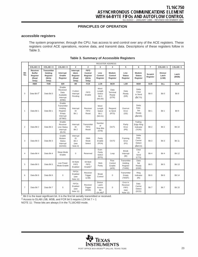
accessible registers
The system programmer, through the CPU, has access to and control over any of the ACE registers. Theseregisters control ACE operations, receive data, and transmit data. Descriptions of these registers follow inTable 3.
Table 3. Summary of Accessible Registers
REGISTER ADDRESS
0 DLAB = 0 0 DLAB = 0 1 DLAB = 0 2 2 3 4 5 6 7 0 DLAB = 1 1 DLAB = 1
ReceiverBuffer
Register(ReadOnly)
TransmitterHoldingRegister
(WriteOnly)
Interrupt Enable
Register
Interrupt Ident.
Register(ReadOnly)
FIFOControlRegister
(WriteOnly)
Line ControlRegister
Modem ControlRegister
Line Status
Register
Modem Status
Register
ScratchRegister
DivisorLatch(LSB)
Latch(MSB)
RBR THR IER IIR FCR LCR MCR LSR MSR SCR DLL DLM
0 Data Bit 0† Data Bit 0
EnableReceived
Data AvailableInterrupt(ERBI)
0 wheninterruptPending
FIFOEnable
Word LengthSelectBit 0
(WLS0)
DataTerminalReady(DTR)
DataReady(DR)
DeltaClear
to Send
(∆CTS)
Bit 0 Bit 0 Bit 8
1 Data Bit 1 Data Bit 1
EnableTransmitter
Holding Register
EmptyInterrupt(ETBEI)
InterruptID
Bit 1
ReceiverFIFOReset
Word LengthSelectBit 1
(WLS1)
Requestto Send(RTS)
OverrunError(OE)
DeltaData Set
Ready
(∆DSR)
Bit 1 Bit 1 Bit 9
2 Data Bit 2 Data Bit 2
EnableReceiver
Line StatusInterrupt(ELSI)
InterruptID
Bit 2
TransmitterFIFOReset
Numberof
Stop Bits(STB)
OUT1ParityError(PE)
Trailing Edge RingIndicator(TERI)
Bit 2 Bit 2 Bit 10
3 Data Bit 3 Data Bit 3
EnableModem Status
Interrupt(EDSSI)
InterruptID
Bit 2(see
Note 4)
DMAModeSelect
ParityEnable(PEN)
OUT2Framing
Error(FE)
DeltaData
CarrierDetect
(∆DCD)
Bit 3 Bit 3 Bit 11
4 Data Bit 4 Data Bit 4Sleep Mode
Enable0 Reserved
Even ParitySelect(EPS)
LoopBreak
Interrupt(BI)
Clearto
Send(CTS)
Bit 4 Bit 4 Bit 12
5 Data Bit 5 Data Bit 5Low Power
Mode Enable
64 ByteFIFO
Enabled
64 ByteFIFO
Enable‡
StickParity
Flow ControlEnable(AFE)
TransmitterHoldingRegister(THRE)
DataSet
Ready(DSR)
Bit 5 Bit 5 Bit 13
6 Data Bit 6 Data Bit 6 0
FIFOsEnabled
(seeNote 11)
ReceiverTrigger(LSB)
BreakControl
0Transmitter
Empty(TEMT)
RingIndicator
(RI)Bit 6 Bit 6 Bit 14
7 Data Bit 7 Data Bit 7 0
FIFOsEnabled
(seeNote 11)
ReceiverTrigger(MSB)
Divisor Latch
AccessBit
(DLAB)‡
0
Error inReceiver
FIFO(see
Note 12)
Data CarrierDetect(DCD)
Bit 7 Bit 7 Bit 15
† Bit 0 is the least significant bit. It is the first bit serially transmitted or received.‡ Access to DLAB LSB, MSB, and FCR bit 5 require LCR bit 7 = 1NOTE 11: These bits are always 0 in the TL16C450 mode.
TL16C750ASYNCHRONOUS COMMUNICATIONS ELEMENTWITH 64-BYTE FIFOs AND AUTOFLOW CONTROLSLLS191C – JANUARY 1995 – REVISED DECEMBER 1997
24 POST OFFICE BOX 655303 • DALLAS, TEXAS 75265
PRINCIPLES OF OPERATION
FIFO control register (FCR)
The FCR is a write-only register at the same location as the IIR, which is a read-only register. The FCR enablesthe FIFOs, clears the FIFOs, sets the receiver FIFO trigger level, and selects the type of DMA signaling.
Bit 0: FCR0 when set enables the transmit and receive FIFOs. This bit must be set when other FCR bitsare written to or they are not programmed. Changing this bit clears the FIFOs.
Bit 1: FCR1 when set clears all bytes in the receiver FIFO and resets its counter. The RSR is not cleared.The logic 1 that is written to this bit position is self clearing.
Bit 2: FCR2 when set clears all bytes in the transmit FIFO and resets its counter to 0. The TSR is notcleared. The logic 1 that is written to this bit position is self clearing.
Bit 3: When FCR0 is set, setting FCR3 causes the RXRDY and TXRDY to change from mode 0 tomode 1.
Bit 4: Reserved for future use.
Bit 5: When this bit is set 64-byte mode of operation is selected. When cleared, the 16-byte mode isselected. A write to FCR bit 5 is protected by setting the line control register (LCR) bit 7 = 1. LCR bit 7 needsto cleared for normal operation.
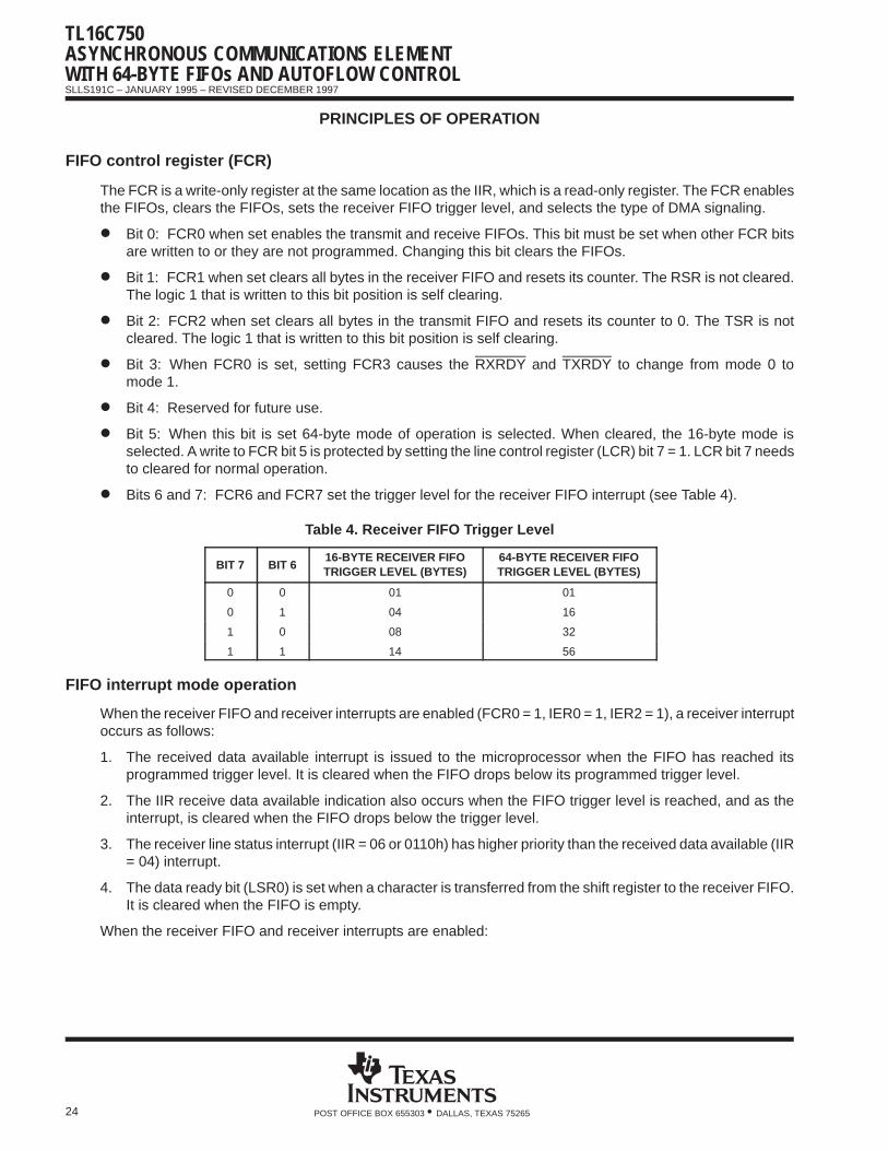
Bits 6 and 7: FCR6 and FCR7 set the trigger level for the receiver FIFO interrupt (see Table 4).
Table 4. Receiver FIFO Trigger Level
BIT 7 BIT 616-BYTE RECEIVER FIFOTRIGGER LEVEL (BYTES)
64-BYTE RECEIVER FIFOTRIGGER LEVEL (BYTES)
0 0 01 01
0 1 04 16
1 0 08 32
1 1 14 56
FIFO interrupt mode operation
When the receiver FIFO and receiver interrupts are enabled (FCR0 = 1, IER0 = 1, IER2 = 1), a receiver interruptoccurs as follows:
1. The received data available interrupt is issued to the microprocessor when the FIFO has reached itsprogrammed trigger level. It is cleared when the FIFO drops below its programmed trigger level.
2. The IIR receive data available indication also occurs when the FIFO trigger level is reached, and as theinterrupt, is cleared when the FIFO drops below the trigger level.
3. The receiver line status interrupt (IIR = 06 or 0110h) has higher priority than the received data available (IIR= 04) interrupt.
4. The data ready bit (LSR0) is set when a character is transferred from the shift register to the receiver FIFO.It is cleared when the FIFO is empty.
When the receiver FIFO and receiver interrupts are enabled:
TL16C750ASYNCHRONOUS COMMUNICATIONS ELEMENT
WITH 64-BYTE FIFOs AND AUTOFLOW CONTROLSLLS191C – JANUARY 1995 – REVISED DECEMBER 1997
25POST OFFICE BOX 655303 • DALLAS, TEXAS 75265
PRINCIPLES OF OPERATION
FIFO interrupt mode operation (continued)
1. FIFO time-out interrupt occurs when the following conditions exist:
a. At least one character is in the FIFO.
b. The most recent serial character was received more than four continuous character times ago (if twostop bits are programmed, the second one is included in this time delay).
c. The most recent microprocessor read of the FIFO occurred more than four continuous character timesago. This causes a maximum character received to interrupt an issued delay of 160 ms at300 baud with a 12-bit character.
2. Character times are calculated by using RCLK for a clock signal (makes the delay proportional to the baudrate).
3. When a time-out interrupt has occurred, the FIFO interrupt is cleared. The timer is reset when themicroprocessor reads one character from the receiver FIFO. When a time-out interrupt has not occurred,the time-out timer is reset after a new character is received or after the microprocessor reads the receiverFIFO.
When the transmitter FIFO and THRE interrupt are enabled (FCR0 = 1, IER1 = 1), transmit interrupts occur asfollows:
1. The transmitter holding register interrupt [IIR (3–0) = 2] occurs when the transmit FIFO is empty. Thetransmit FIFO is cleared [IIR (3–0) = 1] when the THR is written to (1 to 16 characters may be written tothe transmit FIFO while servicing this interrupt) or the IIR is read.
2. The transmit FIFO empty indicator (LSR5 (THRE) = 1) is delayed one character time minus the last stopbit time when there have not been at least two bytes in the transmit FIFO at the same time since the lasttime that THRE = 1. The first transmitter interrupt after changing FCR0 is immediate when it is enabled.
Character time-out and receiver FIFO trigger level interrupts have the same priority as the current received dataavailable interrupt; transmit FIFO empty has the same priority as the current THRE interrupt.
FIFO polled mode operation
With FCR0 = 1 (transmitter and receiver FIFOs enabled), clearing IER0, IER1, IER2, IER3, or all four to 0 putsthe ACE in the FIFO polled mode of operation. Since the receiver and transmitter are controlled separately,either one or both can be in the polled mode of operation.
In this mode, the user program checks receiver and transmitter status using the LSR. As stated previously:
• LSR0 is set when there is at least one byte in the receiver FIFO.
• LSR (1–4) specify which error(s) have occurred. Character error status is handled the same way aswhen in the interrupt mode; the IIR is not affected since IER2 = 0.
• LSR5 indicates when the THR is empty.
• LSR6 indicates that both the THR and TSR are empty.
• LSR7 indicates whether there are any errors in the receiver FIFO.
There is no trigger level reached or time-out condition indicated in the FIFO polled mode. However, the receiverand transmitter FIFOs are still fully capable of holding characters.
TL16C750ASYNCHRONOUS COMMUNICATIONS ELEMENTWITH 64-BYTE FIFOs AND AUTOFLOW CONTROLSLLS191C – JANUARY 1995 – REVISED DECEMBER 1997
26 POST OFFICE BOX 655303 • DALLAS, TEXAS 75265
PRINCIPLES OF OPERATION
interrupt enable register (IER)
The IER enables each of the five types of interrupts (refer to Table 5) and the INTRPT signal in response to aninterrupt generation. The IER can also disable the interrupt system by clearing bits 0 through 3. The contentsof this register are summarized in Table3 and are described in the following bulleted list.
Bit 0: When set, this bit enables the received data available interrupt.
Bit 1: When set, this bit enables the THRE interrupt.
Bit 2: When set, this bit enables the receiver line status interrupt.
Bit 3: When set, this bit enables the modem status interrupt.
Bit 4: When set, this bit enables sleep mode. The ACE is always awake when there is a byte in thetransmitter, activity on the SIN, or when the device is in the loopback mode. The ACE is also awake wheneither ∆CTS, ∆DSR, ∆DCD, or TERI = 1. Bit 4 must be set to enable sleep mode.
Bit 5: When set, this bit enables low-power mode. Low-power mode functions similar to sleep mode.However, this feature powers down the clock to the ACE only, while keeping the oscillator running. Bit 5 mustbe set to enable low-power mode.
Bits 6 and 7: Not used (always cleared)
interrupt identification register (IIR)
The ACE has an on-chip interrupt generation and prioritization capability that permits a flexible interface withmost popular microprocessors.
The ACE provides four prioritized levels of interrupts:
Priority 1 – Receiver line status (highest priority)
Priority 2 – Receiver data ready or receiver character timeout
Priority 3 –Transmitter holding register empty
Priority 4–Modem status (lowest priority)
When an interrupt is generated, the IIR indicates that an interrupt is pending and provides the type of interruptin its three least significant bits (bits 0, 1, and 2). The contents of this register are summarized in Table 3 anddescribed in Table 5. Details on each bit are as follows:
Bit 0: This bit can be used either in a hardwire prioritized, or polled interrupt system. When this bit is cleared,an interrupt is pending. When bit 0 is set, no interrupt is pending.
Bits 1 and 2: Used to identify the highest priority interrupt pending as indicated in Table 3.
Bit 3: This bit is always cleared in the TL16C450 mode. In FIFO mode, this bit is set with bit 2 to indicatethat a time-out interrupt is pending.
Bit 4: Not used (always cleared)
Bits 5, 6, and 7: These bits are to verify the FIFO operation. When all 3 bits are cleared, TL16C450 modeis chosen. When bits 6 and 7 are set and bit 5 is cleared, 16-byte mode is chosen. When bits 5, 6, and 7are set, 64-byte mode is chosen.
TL16C750ASYNCHRONOUS COMMUNICATIONS ELEMENT
WITH 64-BYTE FIFOs AND AUTOFLOW CONTROLSLLS191C – JANUARY 1995 – REVISED DECEMBER 1997
27POST OFFICE BOX 655303 • DALLAS, TEXAS 75265
PRINCIPLES OF OPERATION
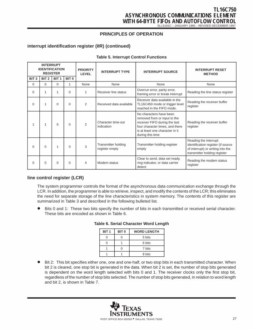
interrupt identification register (IIR) (continued)
Table 5. Interrupt Control Functions
INTERRUPT IDENTIFICATION
REGISTERPRIORITY
LEVELINTERRUPT TYPE INTERRUPT SOURCE
INTERRUPT RESETMETHOD
BIT 3 BIT 2 BIT 1 BIT 0
0 0 0 1 None None None None
0 1 1 0 1 Receiver line statusOverrun error, parity error,framing error or break interrupt
Reading the line status register
0 1 0 0 2 Received data availableReceiver data available in theTL16C450 mode or trigger levelreached in the FIFO mode.
Reading the receiver bufferregister
1 1 0 0 2Character time-outindication
No characters have beenremoved from or input to thereceiver FIFO during the lastfour character times, and thereis at least one character in itduring this time
Reading the receiver bufferregister
0 0 1 0 3Transmitter holding register empty
Transmitter holding registerempty
Reading the interruptidentification register (if sourceof interrupt) or writing into thetransmitter holding register
0 0 0 0 4 Modem statusClear to send, data set ready,ring indicator, or data carrierdetect
Reading the modem statusregister
line control register (LCR)
The system programmer controls the format of the asynchronous data communication exchange through theLCR. In addition, the programmer is able to retrieve, inspect, and modify the contents of the LCR; this eliminatesthe need for separate storage of the line characteristics in system memory. The contents of this register aresummarized in Table 3 and described in the following bulleted list.
Bits 0 and 1: These two bits specify the number of bits in each transmitted or received serial character.These bits are encoded as shown in Table 6.
Table 6. Serial Character Word Length
BIT 1 BIT 0 WORD LENGTH
0 0 5 bits
0 1 6 bits
1 0 7 bits
1 1 8 bits
Bit 2: This bit specifies either one, one and one-half, or two stop bits in each transmitted character. Whenbit 2 is cleared, one stop bit is generated in the data. When bit 2 is set, the number of stop bits generatedis dependent on the word length selected with bits 0 and 1. The receiver clocks only the first stop bit,regardless of the number of stop bits selected. The number of stop bits generated, in relation to word lengthand bit 2, is shown in Table 7.
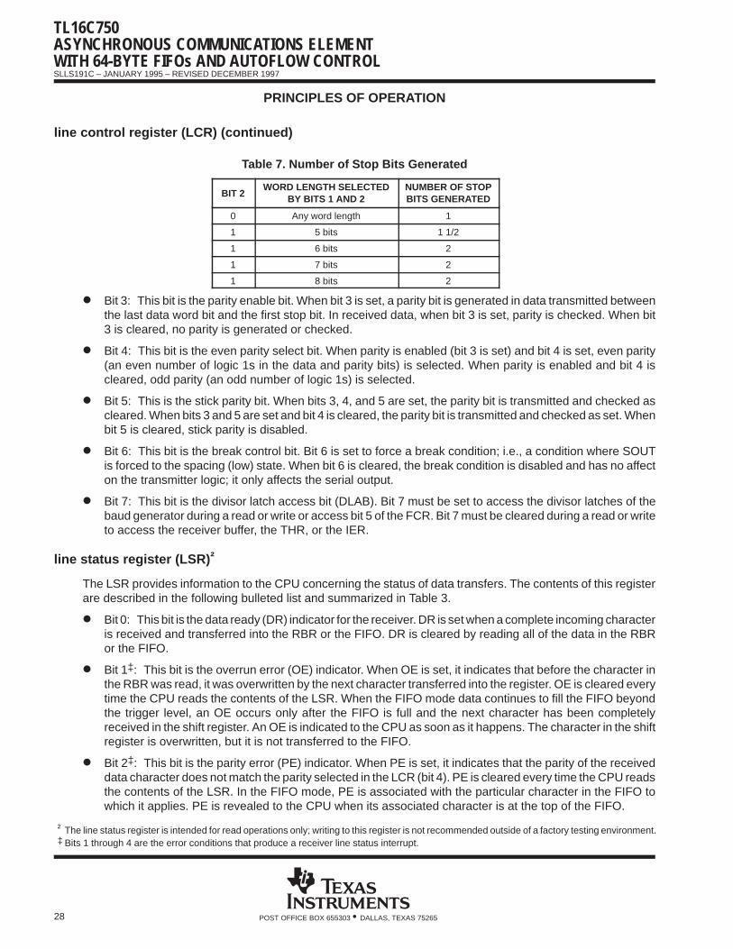
TL16C750ASYNCHRONOUS COMMUNICATIONS ELEMENTWITH 64-BYTE FIFOs AND AUTOFLOW CONTROLSLLS191C – JANUARY 1995 – REVISED DECEMBER 1997
28 POST OFFICE BOX 655303 • DALLAS, TEXAS 75265
PRINCIPLES OF OPERATION
line control register (LCR) (continued)
Table 7. Number of Stop Bits Generated
BIT 2WORD LENGTH SELECTED
BY BITS 1 AND 2NUMBER OF STOPBITS GENERATED
0 Any word length 1
1 5 bits 1 1/2
1 6 bits 2
1 7 bits 2
1 8 bits 2
Bit 3: This bit is the parity enable bit. When bit 3 is set, a parity bit is generated in data transmitted betweenthe last data word bit and the first stop bit. In received data, when bit 3 is set, parity is checked. When bit3 is cleared, no parity is generated or checked.
Bit 4: This bit is the even parity select bit. When parity is enabled (bit 3 is set) and bit 4 is set, even parity(an even number of logic 1s in the data and parity bits) is selected. When parity is enabled and bit 4 iscleared, odd parity (an odd number of logic 1s) is selected.
Bit 5: This is the stick parity bit. When bits 3, 4, and 5 are set, the parity bit is transmitted and checked ascleared. When bits 3 and 5 are set and bit 4 is cleared, the parity bit is transmitted and checked as set. Whenbit 5 is cleared, stick parity is disabled.
Bit 6: This bit is the break control bit. Bit 6 is set to force a break condition; i.e., a condition where SOUTis forced to the spacing (low) state. When bit 6 is cleared, the break condition is disabled and has no affecton the transmitter logic; it only affects the serial output.
Bit 7: This bit is the divisor latch access bit (DLAB). Bit 7 must be set to access the divisor latches of thebaud generator during a read or write or access bit 5 of the FCR. Bit 7 must be cleared during a read or writeto access the receiver buffer, the THR, or the IER.
line status register (LSR) †
The LSR provides information to the CPU concerning the status of data transfers. The contents of this registerare described in the following bulleted list and summarized in Table 3.
Bit 0: This bit is the data ready (DR) indicator for the receiver. DR is set when a complete incoming characteris received and transferred into the RBR or the FIFO. DR is cleared by reading all of the data in the RBRor the FIFO.
Bit 1‡: This bit is the overrun error (OE) indicator. When OE is set, it indicates that before the character inthe RBR was read, it was overwritten by the next character transferred into the register. OE is cleared everytime the CPU reads the contents of the LSR. When the FIFO mode data continues to fill the FIFO beyondthe trigger level, an OE occurs only after the FIFO is full and the next character has been completelyreceived in the shift register. An OE is indicated to the CPU as soon as it happens. The character in the shiftregister is overwritten, but it is not transferred to the FIFO.
Bit 2‡: This bit is the parity error (PE) indicator. When PE is set, it indicates that the parity of the receiveddata character does not match the parity selected in the LCR (bit 4). PE is cleared every time the CPU readsthe contents of the LSR. In the FIFO mode, PE is associated with the particular character in the FIFO towhich it applies. PE is revealed to the CPU when its associated character is at the top of the FIFO.
† The line status register is intended for read operations only; writing to this register is not recommended outside of a factory testing environment.‡ Bits 1 through 4 are the error conditions that produce a receiver line status interrupt.
TL16C750ASYNCHRONOUS COMMUNICATIONS ELEMENT
WITH 64-BYTE FIFOs AND AUTOFLOW CONTROLSLLS191C – JANUARY 1995 – REVISED DECEMBER 1997
29POST OFFICE BOX 655303 • DALLAS, TEXAS 75265
PRINCIPLES OF OPERATION
line status register (LSR) † (continued)
Bit 3‡: This bit is the framing error (FE) indicator. When FE is set, it indicates that the received characterdoes not have a valid (set) stop bit. FE is cleared every time the CPU reads the contents of the LSR. In theFIFO mode, this error is associated with the particular character in the FIFO to which it applies. FE isrevealed to the CPU when its associated character is at the top of the FIFO. The ACE tries to resynchronizeafter a FE. To accomplish this, it is assumed that the FE is due to the next start bit. The ACE samples thisstart bit twice and then accepts the input data.
Bit 4: This bit is the break interrupt (BI) indicator. When BI is set, it indicates that the received data inputwas held in the low state for longer than a full-word transmission time. A full-word transmission time isdefined as the total time to transmit the start, data, parity, and stop bits. BI is cleared every time the CPUreads the contents of the LSR. In the FIFO mode, BI is associated with the particular character in the FIFOto which it applies. BI is revealed to the CPU when its associated character is at the top of the FIFO. Whena break occurs, only one 0 character is loaded into the FIFO. The next character transfer is enabled afterSIN goes to the marking state for at least two RCLK samples and then receives the next valid start bit.
Bit 5: This bit is the transmitter holding register empty (THRE) indicator. THRE is set when the THR isempty, indicating that the ACE is ready to accept a new character. If the THRE interrupt is enabled whenTHRE is set, an interrupt is generated. THRE is set when the contents of the THR are transferred to theTSR. THRE is cleared concurrent with the loading of the THR by the CPU. In the FIFO mode, THRE is setwhen the transmit FIFO is empty; it is cleared when at least one byte is written to the transmit FIFO.
Bit 6: This bit is the transmitter empty (TEMT) indicator. TEMT bit is set when the THR and the TSR areboth empty. When either the THR or the TSR contains a data character, TEMT is cleared. In the FIFO mode,TEMT is set when the transmitter FIFO and TSR are both empty.
Bit 7: In TL16C750 mode and in TL16C450 mode, this bit is always cleared. In the FIFO mode, LSR7 isset when there is at least one parity, framing, or break error in the FIFO. It is cleared when themicroprocessor reads the LSR and there are no subsequent errors in the FIFO.
modem control register (MCR)
The MCR is an 8-bit register that controls an interface with a modem, data set, or peripheral device that isemulating a modem. The contents of this register are summarized in Table 3 and are described in the followingbulleted list.
Bit 0: This bit (DTR) controls the DTR output.
Bit 1: This bit (RTS) controls RTS output.
Bit 2: This bit (OUT1) controls OUT1 signal.
Bit 3: This bit (OUT2) controls the OUT2 signal.
When any of bits 0 through 3 is set, the associated output is forced low; a cleared bit forces the associated outputhigh.
† The line status register is intended for read operations only; writing to this register is not recommended outside of a factory testing environment.‡ Bits 1 through 4 are the error conditions that produce a receiver line status interrupt.
TL16C750ASYNCHRONOUS COMMUNICATIONS ELEMENTWITH 64-BYTE FIFOs AND AUTOFLOW CONTROLSLLS191C – JANUARY 1995 – REVISED DECEMBER 1997
30 POST OFFICE BOX 655303 • DALLAS, TEXAS 75265
PRINCIPLES OF OPERATION
modem control register (MCR) (continued)
Bit 4: This bit (LOOP) provides a local loop back feature for diagnostic testing of the ACE. When LOOPis set, the following occurs:
– SOUT is asserted high.
– SIN is disconnected.
– The output of the TSR is looped back into the RSR input.
– The four modem control inputs (CTS, DSR, DCD, and RI) are disconnected.
– The four modem control outputs (DTR, RTS, OUT1, and OUT2) are internally connected to the fourmodem control inputs.
– The four modem control outputs are forced to their inactive (high) states.
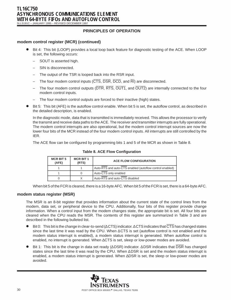
Bit 5: This bit (AFE) is the autoflow control enable. When bit 5 is set, the autoflow control, as described inthe detailed description, is enabled.
In the diagnostic mode, data that is transmitted is immediately received. This allows the processor to verifythe transmit and receive data paths to the ACE. The receiver and transmitter interrupts are fully operational.The modem control interrupts are also operational, but the modem control interrupt sources are now thelower four bits of the MCR instead of the four modem control inputs. All interrupts are still controlled by theIER.
The ACE flow can be configured by programming bits 1 and 5 of the MCR as shown in Table 8.
Table 8. ACE Flow Configuration
MCR BIT 5(AFE)
MCR BIT 1(RTS) ACE FLOW CONFIGURATION
1 1 Auto-RTS and auto-CTS enabled (autoflow control enabled)
1 0 Auto-CTS only enabled
0 X Auto-RTS and auto-CTS disabled
When bit 5 of the FCR is cleared, there is a 16-byte AFC. When bit 5 of the FCR is set, there is a 64-byte AFC.
modem status register (MSR)
The MSR is an 8-bit register that provides information about the current state of the control lines from themodem, data set, or peripheral device to the CPU. Additionally, four bits of this register provide changeinformation. When a control input from the modem changes state, the appropriate bit is set. All four bits arecleared when the CPU reads the MSR. The contents of this register are summarized in Table 3 and aredescribed in the following bulleted list.
Bit 0: This bit is the change in clear-to-send (∆CTS) indicator. ∆CTS indicates that CTS has changed statessince the last time it was read by the CPU. When ∆CTS is set (autoflow control is not enabled and themodem status interrupt is enabled), a modem status interrupt is generated. When autoflow control isenabled, no interrupt is generated. When ∆CTS is set, sleep or low-power modes are avoided.
Bit 1: This bit is the change in data set ready (∆DSR) indicator. ∆DSR indicates that DSR has changedstates since the last time it was read by the CPU. When ∆DSR is set and the modem status interrupt isenabled, a modem status interrupt is generated. When ∆DSR is set, the sleep or low-power modes areavoided.
TL16C750ASYNCHRONOUS COMMUNICATIONS ELEMENT
WITH 64-BYTE FIFOs AND AUTOFLOW CONTROLSLLS191C – JANUARY 1995 – REVISED DECEMBER 1997
31POST OFFICE BOX 655303 • DALLAS, TEXAS 75265
PRINCIPLES OF OPERATION
modem status register (MSR) (continued)
Bit 2: This bit is the trailing edge of the ring indicator (TERI) detector. TERI indicates that RI to the chip haschanged from a low to a high level. When TERI is set and the modem status interrupt is enabled, a modemstatus interrupt is generated. When TERI is set, sleep or low-power modes are avoided.
Bit 3: This bit is the change in data carrier detect (∆DCD) indicator. ∆DCD indicates that DCD to the chiphas changed states since the last time it was read by the CPU. When ∆DCD is set and the modem statusinterrupt is enabled, a modem status interrupt is generated. When ∆DCD is set, sleep or low-power modesare avoided.
Bit 4: This bit is the complement of CTS. When the ACE is in the diagnostic test mode (LOOP [MCR4] = 1), this bit is equal to the MCR bit 1 (RTS).
Bit 5: This bit is the complement of DSR input. When the ACE is in the diagnostic test mode (LOOP [MCR4] = 1), this bit is equal to the MCR bit 0 (DTR).
Bit 6: This bit is the complement of RI. When the ACE is in the diagnostic test mode (LOOP [MCR4] = 1),this bit is equal to the MCR bit 2 (OUT1).
Bit 7: This bit is the complement of DCD. When the ACE is in the diagnostic test mode (LOOP [MCR4] = 1), this bit is equal to the MCR bit 3 (OUT2).
programmable baud generator
The ACE contains a programmable baud generator that takes a clock input in the range between dc and 16 MHzand divides it by a divisor in the range between 1 and (216–1). The output frequency of the baud generator is16× the baud rate. The formula for the divisor is:
divisor = XIN frequency input ÷ (desired baud rate × 16)
Two 8-bit registers, called divisor latches, store the divisor in a 16-bit binary format. These divisor latches mustbe loaded during initialization of the ACE to ensure desired operation of the baud generator. When either of thedivisor latches is loaded, a 16-bit baud counter is also loaded to prevent long counts on initial load.
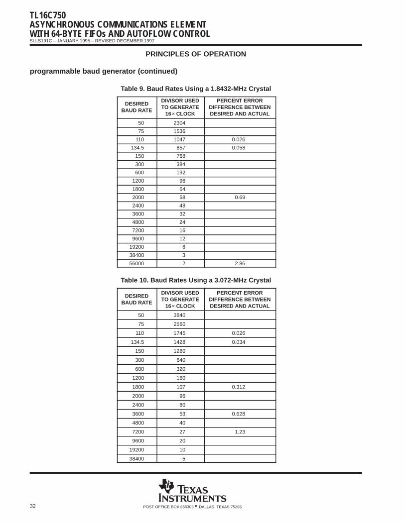
Tables 9 and 10 illustrate the use of the baud generator with crystal frequencies of 1.8432 MHz and 3.072 MHzrespectively. For baud rates of 38.4 kbits/s and below, the error obtained is very small. The accuracy of theselected baud rate is dependent on the selected crystal frequency (see Figure 21).
TL16C750ASYNCHRONOUS COMMUNICATIONS ELEMENTWITH 64-BYTE FIFOs AND AUTOFLOW CONTROLSLLS191C – JANUARY 1995 – REVISED DECEMBER 1997
32 POST OFFICE BOX 655303 • DALLAS, TEXAS 75265
PRINCIPLES OF OPERATION
programmable baud generator (continued)
Table 9. Baud Rates Using a 1.8432-MHz Crystal
DESIREDBAUD RATE
DIVISOR USEDTO GENERATE
16× CLOCK
PERCENT ERRORDIFFERENCE BETWEENDESIRED AND ACTUAL
50 2304
75 1536
110 1047 0.026
134.5 857 0.058
150 768
300 384
600 192
1200 96
1800 64
2000 58 0.69
2400 48
3600 32
4800 24
7200 16
9600 12
19200 6
38400 3
56000 2 2.86
Table 10. Baud Rates Using a 3.072-MHz Crystal
DESIREDBAUD RATE
DIVISOR USEDTO GENERATE
16× CLOCK
PERCENT ERRORDIFFERENCE BETWEENDESIRED AND ACTUAL
50 3840
75 2560
110 1745 0.026
134.5 1428 0.034
150 1280
300 640
600 320
1200 160
1800 107 0.312
2000 96
2400 80
3600 53 0.628
4800 40
7200 27 1.23
9600 20
19200 10
38400 5
TL16C750ASYNCHRONOUS COMMUNICATIONS ELEMENT
WITH 64-BYTE FIFOs AND AUTOFLOW CONTROLSLLS191C – JANUARY 1995 – REVISED DECEMBER 1997
33POST OFFICE BOX 655303 • DALLAS, TEXAS 75265
PRINCIPLES OF OPERATION
programmable baud generator (continued)
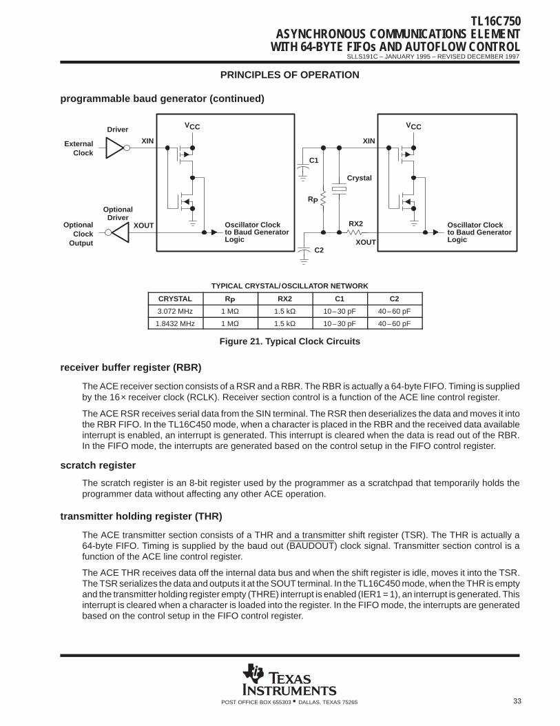
Driver
OptionalDriver
ExternalClock
OptionalClock
Output
Oscillator Clockto Baud GeneratorLogic
XIN
XOUT
VCC
Crystal
XIN
RX2
VCC
XOUT
C1
RP
C2
Oscillator Clockto Baud GeneratorLogic
TYPICAL CRYSTAL/OSCILLATOR NETWORK
CRYSTAL RP RX2 C1 C2
3.072 MHz 1 MΩ 1.5 kΩ 10–30 pF 40–60 pF
1.8432 MHz 1 MΩ 1.5 kΩ 10–30 pF 40–60 pF
Figure 21. Typical Clock Circuits
receiver buffer register (RBR)
The ACE receiver section consists of a RSR and a RBR. The RBR is actually a 64-byte FIFO. Timing is suppliedby the 16× receiver clock (RCLK). Receiver section control is a function of the ACE line control register.
The ACE RSR receives serial data from the SIN terminal. The RSR then deserializes the data and moves it intothe RBR FIFO. In the TL16C450 mode, when a character is placed in the RBR and the received data availableinterrupt is enabled, an interrupt is generated. This interrupt is cleared when the data is read out of the RBR.In the FIFO mode, the interrupts are generated based on the control setup in the FIFO control register.
scratch register
The scratch register is an 8-bit register used by the programmer as a scratchpad that temporarily holds theprogrammer data without affecting any other ACE operation.
transmitter holding register (THR)
The ACE transmitter section consists of a THR and a transmitter shift register (TSR). The THR is actually a64-byte FIFO. Timing is supplied by the baud out (BAUDOUT) clock signal. Transmitter section control is afunction of the ACE line control register.
The ACE THR receives data off the internal data bus and when the shift register is idle, moves it into the TSR.The TSR serializes the data and outputs it at the SOUT terminal. In the TL16C450 mode, when the THR is emptyand the transmitter holding register empty (THRE) interrupt is enabled (IER1 = 1), an interrupt is generated. Thisinterrupt is cleared when a character is loaded into the register. In the FIFO mode, the interrupts are generatedbased on the control setup in the FIFO control register.
PACKAGING INFORMATION
Orderable Device Status (1) PackageType
PackageDrawing
Pins PackageQty
Eco Plan (2) Lead/Ball Finish MSL Peak Temp (3)
TL16C750FN ACTIVE PLCC FN 44 26 Green (RoHS &no Sb/Br)
CU NIPDAU Level-3-260C-168 HR
TL16C750FNG4 ACTIVE PLCC FN 44 26 Green (RoHS &no Sb/Br)
CU NIPDAU Level-3-260C-168 HR
TL16C750FNR ACTIVE PLCC FN 44 500 Green (RoHS &no Sb/Br)
CU NIPDAU Level-3-260C-168 HR
TL16C750FNRG4 ACTIVE PLCC FN 44 500 Green (RoHS &no Sb/Br)
CU NIPDAU Level-3-260C-168 HR
TL16C750IPM ACTIVE LQFP PM 64 160 Green (RoHS &no Sb/Br)
CU NIPDAU Level-3-260C-168 HR
TL16C750IPMG4 ACTIVE LQFP PM 64 160 Green (RoHS &no Sb/Br)
CU NIPDAU Level-3-260C-168 HR
TL16C750PM ACTIVE LQFP PM 64 160 Green (RoHS &no Sb/Br)
CU NIPDAU Level-3-260C-168 HR
TL16C750PMG4 ACTIVE LQFP PM 64 160 Green (RoHS &no Sb/Br)
CU NIPDAU Level-3-260C-168 HR
TL16C750Y OBSOLETE DIESALE Y 0 TBD Call TI Call TI
(1) The marketing status values are defined as follows:ACTIVE: Product device recommended for new designs.LIFEBUY: TI has announced that the device will be discontinued, and a lifetime-buy period is in effect.NRND: Not recommended for new designs. Device is in production to support existing customers, but TI does not recommend using this part ina new design.PREVIEW: Device has been announced but is not in production. Samples may or may not be available.OBSOLETE: TI has discontinued the production of the device.
(2) Eco Plan - The planned eco-friendly classification: Pb-Free (RoHS), Pb-Free (RoHS Exempt), or Green (RoHS & no Sb/Br) - please checkhttp://www.ti.com/productcontent for the latest availability information and additional product content details.TBD: The Pb-Free/Green conversion plan has not been defined.Pb-Free (RoHS): TI's terms "Lead-Free" or "Pb-Free" mean semiconductor products that are compatible with the current RoHS requirementsfor all 6 substances, including the requirement that lead not exceed 0.1% by weight in homogeneous materials. Where designed to be solderedat high temperatures, TI Pb-Free products are suitable for use in specified lead-free processes.Pb-Free (RoHS Exempt): This component has a RoHS exemption for either 1) lead-based flip-chip solder bumps used between the die andpackage, or 2) lead-based die adhesive used between the die and leadframe. The component is otherwise considered Pb-Free (RoHScompatible) as defined above.Green (RoHS & no Sb/Br): TI defines "Green" to mean Pb-Free (RoHS compatible), and free of Bromine (Br) and Antimony (Sb) based flameretardants (Br or Sb do not exceed 0.1% by weight in homogeneous material)
(3) MSL, Peak Temp. -- The Moisture Sensitivity Level rating according to the JEDEC industry standard classifications, and peak soldertemperature.
Important Information and Disclaimer:The information provided on this page represents TI's knowledge and belief as of the date that it isprovided. TI bases its knowledge and belief on information provided by third parties, and makes no representation or warranty as to theaccuracy of such information. Efforts are underway to better integrate information from third parties. TI has taken and continues to takereasonable steps to provide representative and accurate information but may not have conducted destructive testing or chemical analysis onincoming materials and chemicals. TI and TI suppliers consider certain information to be proprietary, and thus CAS numbers and other limitedinformation may not be available for release.
In no event shall TI's liability arising out of such information exceed the total purchase price of the TI part(s) at issue in this document sold by TIto Customer on an annual basis.
PACKAGE OPTION ADDENDUM
www.ti.com 20-Mar-2008
Addendum-Page 1

IMPORTANT NOTICETexas Instruments Incorporated and its subsidiaries (TI) reserve the right to make corrections, modifications, enhancements, improvements,and other changes to its products and services at any time and to discontinue any product or service without notice. Customers shouldobtain the latest relevant information before placing orders and should verify that such information is current and complete. All products aresold subject to TI’s terms and conditions of sale supplied at the time of order acknowledgment.TI warrants performance of its hardware products to the specifications applicable at the time of sale in accordance with TI’s standardwarranty. Testing and other quality control techniques are used to the extent TI deems necessary to support this warranty. Except wheremandated by government requirements, testing of all parameters of each product is not necessarily performed.TI assumes no liability for applications assistance or customer product design. Customers are responsible for their products andapplications using TI components. To minimize the risks associated with customer products and applications, customers should provideadequate design and operating safeguards.TI does not warrant or represent that any license, either express or implied, is granted under any TI patent right, copyright, mask work right,or other TI intellectual property right relating to any combination, machine, or process in which TI products or services are used. Informationpublished by TI regarding third-party products or services does not constitute a license from TI to use such products or services or awarranty or endorsement thereof. Use of such information may require a license from a third party under the patents or other intellectualproperty of the third party, or a license from TI under the patents or other intellectual property of TI.Reproduction of TI information in TI data books or data sheets is permissible only if reproduction is without alteration and is accompaniedby all associated warranties, conditions, limitations, and notices. Reproduction of this information with alteration is an unfair and deceptivebusiness practice. TI is not responsible or liable for such altered documentation. Information of third parties may be subject to additionalrestrictions.Resale of TI products or services with statements different from or beyond the parameters stated by TI for that product or service voids allexpress and any implied warranties for the associated TI product or service and is an unfair and deceptive business practice. TI is notresponsible or liable for any such statements.TI products are not authorized for use in safety-critical applications (such as life support) where a failure of the TI product would reasonablybe expected to cause severe personal injury or death, unless officers of the parties have executed an agreement specifically governingsuch use. Buyers represent that they have all necessary expertise in the safety and regulatory ramifications of their applications, andacknowledge and agree that they are solely responsible for all legal, regulatory and safety-related requirements concerning their productsand any use of TI products in such safety-critical applications, notwithstanding any applications-related information or support that may beprovided by TI. Further, Buyers must fully indemnify TI and its representatives against any damages arising out of the use of TI products insuch safety-critical applications.TI products are neither designed nor intended for use in military/aerospace applications or environments unless the TI products arespecifically designated by TI as military-grade or "enhanced plastic." Only products designated by TI as military-grade meet militaryspecifications. Buyers acknowledge and agree that any such use of TI products which TI has not designated as military-grade is solely atthe Buyer's risk, and that they are solely responsible for compliance with all legal and regulatory requirements in connection with such use.TI products are neither designed nor intended for use in automotive applications or environments unless the specific TI products aredesignated by TI as compliant with ISO/TS 16949 requirements. Buyers acknowledge and agree that, if they use any non-designatedproducts in automotive applications, TI will not be responsible for any failure to meet such requirements.Following are URLs where you can obtain information on other Texas Instruments products and application solutions:Products ApplicationsAmplifiers amplifier.ti.com Audio www.ti.com/audioData Converters dataconverter.ti.com Automotive www.ti.com/automotiveDSP dsp.ti.com Broadband www.ti.com/broadbandClocks and Timers www.ti.com/clocks Digital Control www.ti.com/digitalcontrolInterface interface.ti.com Medical www.ti.com/medicalLogic logic.ti.com Military www.ti.com/militaryPower Mgmt power.ti.com Optical Networking www.ti.com/opticalnetworkMicrocontrollers microcontroller.ti.com Security www.ti.com/securityRFID www.ti-rfid.com Telephony www.ti.com/telephonyRF/IF and ZigBee® Solutions www.ti.com/lprf Video & Imaging www.ti.com/video
Wireless www.ti.com/wireless
Mailing Address: Texas Instruments, Post Office Box 655303, Dallas, Texas 75265Copyright © 2008, Texas Instruments Incorporated


![X10 Tester - · PDF fileX10_Tester.can Page 3 of 128. 151 BYTE hasToSendWriteColumnConfig = 0; 152 BYTE hasToSendWriteColumnDefault = 0; 153 154 BYTE StartLogicControl[6]; 155 BYTE](https://img.pdfslide.us/doc/110x75/5aa9f1037f8b9a9a188d968e/x10-tester-page-3-of-128-151-byte-hastosendwritecolumnconfig-0-152-byte-hastosendwritecolumndefault.jpg)