Embed Size (px)
Citation preview

DS04-27260-1EaFUJITSU MICROELECTRONICSDATA SHEET
ASSP For Power Management Applications(General Purpose DC/DC Converter)2ch DC/DC Converter IC withSynchronous Rectification
MB39C011A DESCRIPTION
The MB39C011A is a two-channel DC/DC converter IC suitable for down-conversion that utilizes synchronous rectification and pulse width modulation (PWM). The MB39C011A can operate over a wide range of power supplyvoltages (4.5 V to 17 V), making it optimal as a built-in power supply in digital audio visual equipment and variousother electronic devices.
FEATURES • Wide range of power supply voltages : 4.5 V to 17 V• Supports high frequency operation : 2.0 MHz (Max) • Supports synchronous rectification method (CH1,CH2) • An arbitrary output voltage can be configured using an external resistance.• Built-in standby function : 0 µA (Typ) • Low current consumption : 2.2 mA (Typ, At quiescence) • Built-in soft-start circuit that can control each channel separately independent of the load• Built-in timer latch type short-circuit protection circuit (shares the soft-start capacitor).• Built-in totem pole type output stage for external P-ch/N-ch MOS FET devices• Package : TSSOP-16-pin
APPLICATIONS• Digital TV• Photocopiers• Surveillance cameras• Set-top boxes (STB)• DVD players, DVD recorders• Projectors• IP phones• Vending machines • Consoles and other non-portable devices
Copyright©2007-2008 FUJITSU MICROELECTRONICS LIMITED All rights reserved2007.12
MB39C011A
2
PIN ASSIGNMENT
(TOP VIEW)
(FPT-16P-M07)
VCC
OUT1-1
OUT1-2
VB
RT
FB1
-INE1
CSCP1
VH
OUT2-1
OUT2-2
CTL
GND
FB2
-INE2
CSCP2
1
2
3
4
5
6
7
8
16
15
14
13
12
11
10
9

MB39C011A
PIN DESCRIPTIONS
Pin No. Pin Name I/O Description
1 VCC ⎯ Power supply pin for the reference voltage circuit and control circuit.
2 OUT1-1 OOutput pin for P-ch drive (drives the gate of the external High side FET).
3 OUT1-2 OOutput pin for N-ch drive (drives the gate of the external Low side FET).
4 VB I/O Power supply pin for the N-ch FET drive circuit (VB = 5 V).
5 RT ⎯ Triangular-wave oscillation frequency setting resistor connection pin.
6 FB1 O Error amplifier (Error Amp1) output pin.
7 -INE1 I Error amplifier (Error Amp1) inverted input pin.
8 CSCP1 ⎯ Timer-latch short-circuit protection circuit 1 capacitor connection pin.
9 CSCP2 ⎯ Timer-latch short-circuit protection circuit 2 capacitor connection pin.
10 -INE2 I Error amplifier (Error Amp2) inverted input pin.
11 FB2 O Error amplifier (Error Amp2) output pin.
12 GND ⎯ Ground pin for the reference voltage circuit, control circuit, and output circuit.
13 CTL IPower supply control pin. IC becomes a stand-by mode by setting CTL pin “L” level.
14 OUT2-2 OOutput pin for N-ch drive (drives the gate of the external Low side FET).
15 OUT2-1 OOutput pin for P-ch drive (drives the gate of the external High side FET).
16 VH O Power supply pin for the N-ch FET drive circuit (VH = VCC − 5 V).
3
MB39C011A
4
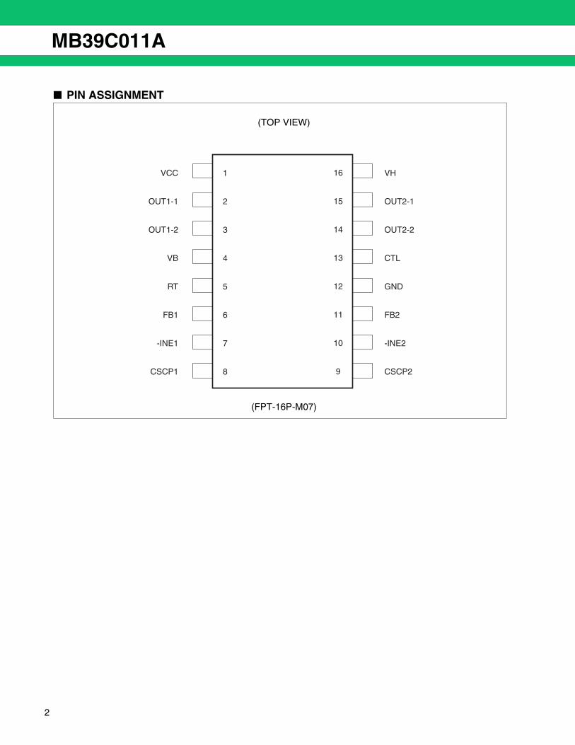
BLOCK DIAGRAM
RT
CT
bias
VB7A
6
2
A
10B
11
B
1
13
125
8
16VH
VH
VB
3
15
14
4
VB
V B VB
9
VIN
(6 V to 17 V)
-INE2
CSCP2
CSCP1
UVLO
Reset
SR Latch
OSC
BiasVoltage
BiasVoltage
VR1Power
ON/OFFCTL
H:ON (Power ON)L:OFF(Standbymode)VTH=1.4 V
GND
(2.0 V)
(2.0 V)
2.5 V
2.5 V
(1.9 V)
SCPComp.1
SCPComp.2
ErrorAmp2
PWMComp.2
ErrorAmp1
PWMComp.1
AS
TA
ST
(1.9 V)
(0.7 V)
(1.7 V)(0.7 V)
(1.7 V)
(1.0 V)
(1.0 V)
(2.3u) (1.0u) (1.0u)(2.3u)
ErrorAmp Ref.(1.0 V)
VB(5 V)
FB1
FB2
-INE1
P-ch
Vcc
Drive1-1
Drive1-2
Drive2-1OUT2-1
step-down
Vo2(3.3 V)
step-down
Vo1(1.8 V)
OUT2-2
OUT1-1
OUT1-2
Drive2-2
N-ch
P-ch
N-ch
<< CH1 >>
<< CH2 >>
CTL
VCC
(Vcc-5 V)

MB39C011A
ABSOLUTE MAXIMUM RATINGS
* : When mounted on a 10 cm square double-sided epoxy circuit board.
WARNING: Semiconductor devices can be permanently damaged by application of stress (voltage, current, temperature, etc.) in excess of absolute maximum ratings. Do not exceed these ratings.
Parameter Symbol ConditionRating
UnitMin Max
Power supply voltage VCC VCC pin ⎯ 18 V
Input voltage
VBVB pin (When VCC pin connected to VB pin)
⎯ 7 V
VINE -INE1, -INE2 pins − 0.3 VB V
VCTL CTL pin ⎯ 18 V
Output current IOOUT1-1, OUT1-2, OUT2-1, OUT2-2 pins
⎯ 60 mA
Peak output current IOP Duty ≤ 5% (t = 1/fosc × Duty) ⎯ 700 mA
Power dissipation PD Ta ≤ + 25 °C ⎯ 1060* mW
Storage temperature TSTG ⎯ − 55 + 125 °C
5
MB39C011A
6
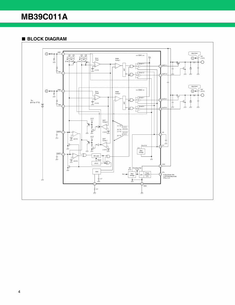
RECOMMENDED OPERATING CONDITIONS
WARNING: The recommended operating conditions are required in order to ensure the normal operation of thesemiconductor device. All of the device’s electrical characteristics are warranted when the device isoperated within these ranges.
Always use semiconductor devices within their recommended operating condition ranges. Operationoutside these ranges may adversely affect reliability and could result in device failure.No warranty is made with respect to uses, operating conditions, or combinations not represented onthe data sheet. Users considering application outside the listed conditions are advised to contact theirrepresentatives beforehand.
Parameter Symbol ConditionValue
UnitMin Typ Max
Power supply voltage VCC VCC pin 4.5 12 17 V
VH pin output current IVH VH pin 0 ⎯ 40 mA
VB pin output current IVB VB pin − 40 ⎯ 0 mA
VB pin input voltage VB
VB pin(When VCC pin connected to VB pin)
4.5 5 6 V
Input voltage VINE -INE1, -INE2 pins 0 ⎯ VB − 0.9 V
CTL pin input voltage VCTL CTL pin 0 ⎯ 17 V
Output current IOUTOUT1-1, OUT1-2, OUT2-1, OUT2-2 pins
− 45 ⎯ + 45 mA
Oscillation frequency fOSC Tj ≤ + 85 °C 100 500 2000 kHz
Timing resistor RT RT pin 3.6 16 100 kΩ
VH pin capacitor CVH VH pin ⎯ 1.0 4.7 µF
VB pin capacitor CVB VB pin ⎯ 1.0 4.7 µF
CSCP1, CSCP2 pin capacitorCSCP1, CSCP2
CSCP1, CSCP2 pins ⎯ 0.047 1.0 µF
Operating ambient temperature
Ta ⎯ − 30 + 25 + 85 °C
MB39C011A
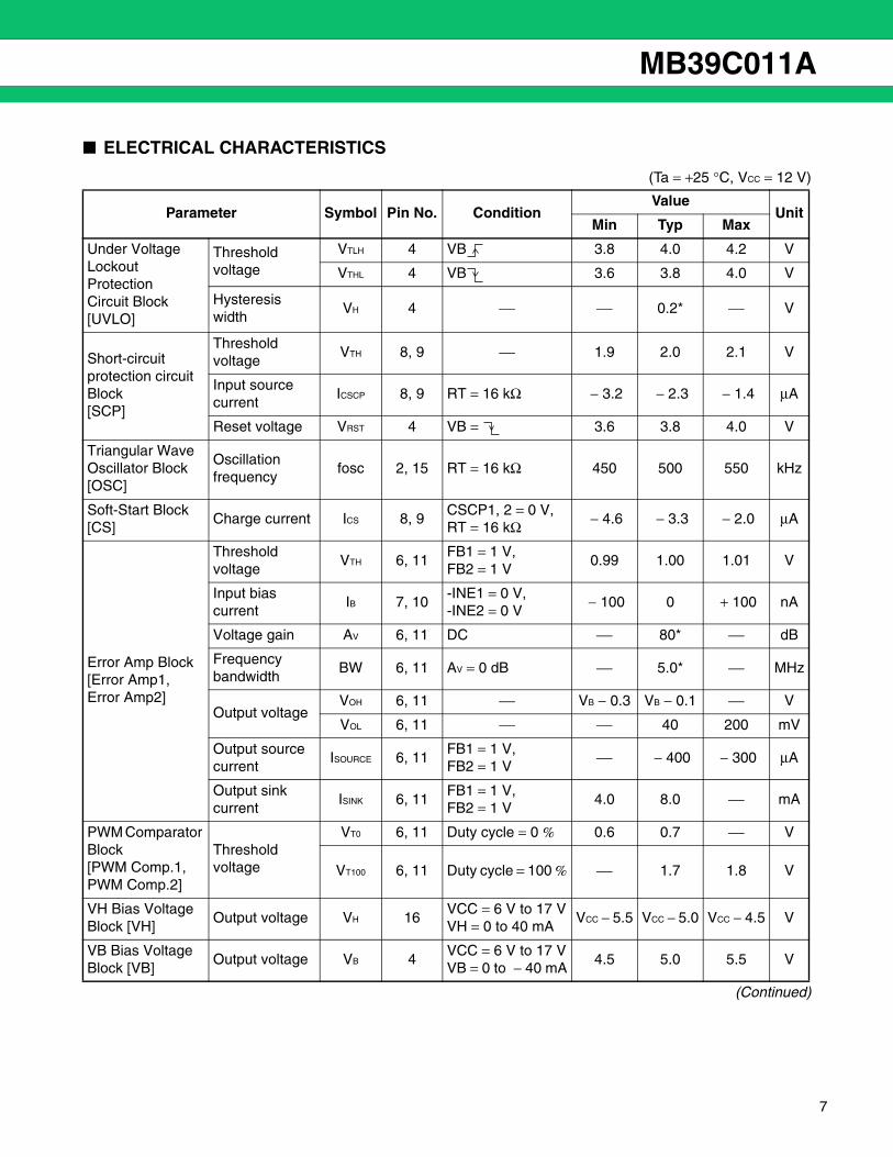
ELECTRICAL CHARACTERISTICS
(Ta = +25 °C, VCC = 12 V)
(Continued)
Parameter Symbol Pin No. ConditionValue
UnitMin Typ Max
Under Voltage Lockout Protection Circuit Block[UVLO]
Threshold voltage
VTLH 4 VB 3.8 4.0 4.2 V
VTHL 4 VB 3.6 3.8 4.0 V
Hysteresis width
VH 4 ⎯ ⎯ 0.2* ⎯ V
Short-circuit protection circuit Block[SCP]
Threshold voltage
VTH 8, 9 ⎯ 1.9 2.0 2.1 V
Input source current
ICSCP 8, 9 RT = 16 kΩ − 3.2 − 2.3 − 1.4 µA
Reset voltage VRST 4 VB = 3.6 3.8 4.0 V
Triangular Wave Oscillator Block [OSC]
Oscillation frequency
fosc 2, 15 RT = 16 kΩ 450 500 550 kHz
Soft-Start Block [CS]
Charge current ICS 8, 9CSCP1, 2 = 0 V, RT = 16 kΩ − 4.6 − 3.3 − 2.0 µA
Error Amp Block [Error Amp1, Error Amp2]
Threshold voltage
VTH 6, 11FB1 = 1 V, FB2 = 1 V
0.99 1.00 1.01 V
Input bias current
IB 7, 10-INE1 = 0 V, -INE2 = 0 V
− 100 0 + 100 nA
Voltage gain AV 6, 11 DC ⎯ 80* ⎯ dB
Frequency bandwidth
BW 6, 11 AV = 0 dB ⎯ 5.0* ⎯ MHz
Output voltageVOH 6, 11 ⎯ VB − 0.3 VB − 0.1 ⎯ V
VOL 6, 11 ⎯ ⎯ 40 200 mV
Output source current
ISOURCE 6, 11FB1 = 1 V, FB2 = 1 V
⎯ − 400 − 300 µA
Output sink current
ISINK 6, 11FB1 = 1 V, FB2 = 1 V
4.0 8.0 ⎯ mA
PWM Comparator Block [PWM Comp.1, PWM Comp.2]
Threshold voltage
VT0 6, 11 Duty cycle = 0 % 0.6 0.7 ⎯ V
VT100 6, 11 Duty cycle = 100 % ⎯ 1.7 1.8 V
VH Bias Voltage Block [VH]
Output voltage VH 16VCC = 6 V to 17 VVH = 0 to 40 mA
VCC − 5.5 VCC − 5.0 VCC − 4.5 V
VB Bias Voltage Block [VB]
Output voltage VB 4VCC = 6 V to 17 VVB = 0 to − 40 mA
4.5 5.0 5.5 V
7
MB39C011A
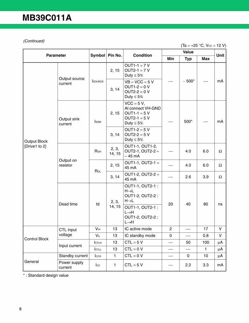
8
(Continued) (Ta = +25 °C, VCC = 12 V)
* : Standard design value
Parameter Symbol Pin No. ConditionValue
UnitMin Typ Max
Output Block[Drive1 to 2]
Output source current
ISOURCE
2, 15OUT1-1 = 7 V OUT2-1 = 7 VDuty ≤ 5%
⎯ − 500* ⎯ mA
3, 14
VB = VCC = 5 VOUT1-2 = 0 V OUT2-2 = 0 VDuty ≤ 5%
Output sink current
ISINK
2, 15
VCC = 5 V, At connect VH-GNDOUT1-1 = 5 VOUT2-1 = 5 V Duty ≤ 5% ⎯ 500* ⎯ mA
3, 14OUT1-2 = 5 VOUT2-2 = 5 VDuty ≤ 5%
Output on resistor
ROH2, 3,
14, 15
OUT1-1, OUT1-2, OUT2-1, OUT2-2 = − 45 mA
⎯ 4.0 6.0 Ω
ROL
2, 15OUT1-1, OUT2-1 = 45 mA
⎯ 4.0 6.0 Ω
3, 14OUT1-2, OUT2-2 = 45 mA
⎯ 2.6 3.9 Ω
Dead time td2, 3,
14, 15
OUT1-1, OUT2-1 : H→LOUT1-2, OUT2-2 : H→L
20 40 80 nsOUT1-1, OUT2-1 : L→HOUT1-2, OUT2-2 : L→H
Control Block
CTL input voltage
VIH 13 IC active mode 2 ⎯ 17 V
VIL 13 IC standby mode 0 ⎯ 0.8 V
Input currentICTLH 13 CTL = 5 V ⎯ 50 100 µA
ICTLL 13 CTL = 0 V ⎯ ⎯ 1 µA
GeneralStandby current ICCS 1 CTL = 0 V ⎯ 0 10 µA
Power supply current
ICC 1 CTL = 5 V ⎯ 2.2 3.3 mA

MB39C011A
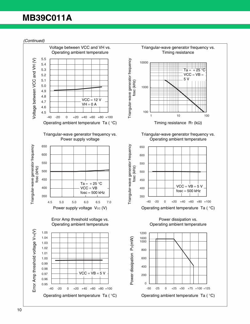
TYPICAL CHARACTERISTICS
(Continued)
Power supply current vs.Power supply voltage
VB bias voltage vs.Power supply voltage
Pow
er s
uppl
y cu
rren
t IC
C (
mA
)
VB
bia
s vo
ltage
VB(V
)
Power supply voltage VCC (V) Power supply voltage VCC (V)
VB bias voltage vs.VB bias output current
VB bias voltage vs.Operating ambient temperature
VB
bia
s vo
ltage
VB (
V)
VB
bia
s vo
ltage
VB (
V)
VB bias output current IVB (mA) Operating ambient temperature Ta ( °C)
Voltage between VCC and VH vs.Power supply voltage
Voltage between VCC and VH vs.VH bias output current
Vol
tage
bet
wee
n V
CC
and
VH
(V
)
Vol
tage
bet
wee
n V
CC
and
VH
(V
)
Power supply voltage VCC (V) VH bias output current IVH (mA)
5.0
4.5
4.0
3.5
3.0
2.5
2.0
1.5
1.0
0.5
0.04 6 8 10 12 14 16 18
Ta = + 25 °C
5.5
5.4
5.3
5.2
5.1
5.0
4.9
4.8
4.7
4.6
4.54 6 8 10 12 14 16 18
Ta = + 25 °CVB = 0 A
5.5
5.4
5.3
5.2
5.1
5.0
4.9
4.8
4.7
4.6
4.5-100 -80 -60 -40 -20 0
Ta = + 25 °CVCC = 12 V
5.5
5.4
5.3
5.2
5.1
5.0
4.9
4.8
4.7
4.6
4.5
-40 -20 0 +20 +40 +60 +80 +100
VCC = 12 V VB = 0 A
5.5
5.4
5.3
5.2
5.1
5.0
4.9
4.8
4.7
4.6
4.54 6 8 10 12 14 16 18
Ta = + 25 °CVH = 0 A
5.5
5.4
5.3
5.2
5.1
5.0
4.9
4.8
4.7
4.6
4.5
0 20 40 60 80 100
Ta = + 25 °CVCC = 12 V
9
MB39C011A
10
(Continued)
Voltage between VCC and VH vs.Operating ambient temperature
Triangular-wave generator frequency vs.Timing resistance
Vol
tage
bet
wee
n V
CC
and
VH
(V
)
Tria
ngul
ar-w
ave
gene
rato
r fr
eque
ncy
fosc
(kH
z)
Operating ambient temperature Ta ( °C) Timing resistance RT (kΩ)
Triangular-wave generator frequency vs.Power supply voltage
Triangular-wave generator frequency vs.Operating ambient temperature
Tria
ngul
ar-w
ave
gene
rato
r fre
quen
cy
fosc
(kH
z)
Tria
ngul
ar-w
ave
gene
rato
r fr
eque
ncy
fosc
(kH
z)
Power supply voltage VCC (V) Operating ambient temperature Ta ( °C)
Error Amp threshold voltage vs.Operating ambient temperature
Power dissipation vs.Operating ambient temperature
Err
or A
mp
thre
shol
d vo
ltage
VT
H(V
)
Pow
er d
issi
patio
n P
D(m
W)
Operating ambient temperature Ta ( °C) Operating ambient temperature Ta ( °C)
5.5
5.4
5.3
5.2
5.1
5.0
4.9
4.8
4.7
4.6
4.5-40 -20 0 +20 +40 +60 +80 +100
VCC = 12 VVH = 0 A
10000
1000
1001 10 100
Ta = + 25 °CVCC = VB = 5 V
650
600
550
500
450
400
350
4.5 5.0 5.0 6.0 6.5 7.0
Ta = + 25 °CVCC = VBfosc = 500 kHz
650
600
550
500
450
400
350
-40 -20 0 +20 +40 +60 +80 +100
VCC = VB = 5 Vfosc = 500 kHz
1.05
1.04
1.03
1.02
1.01
1.00
0.99
0.98
0.97
0.96
0.95-40 -20 0 +20 +40 +60 +80 +100
VCC = VB = 5 V
1200
1000
800
600
400
200
0
1600
-50 -25 0 +25 +50 +75 +100 +125
MB39C011A
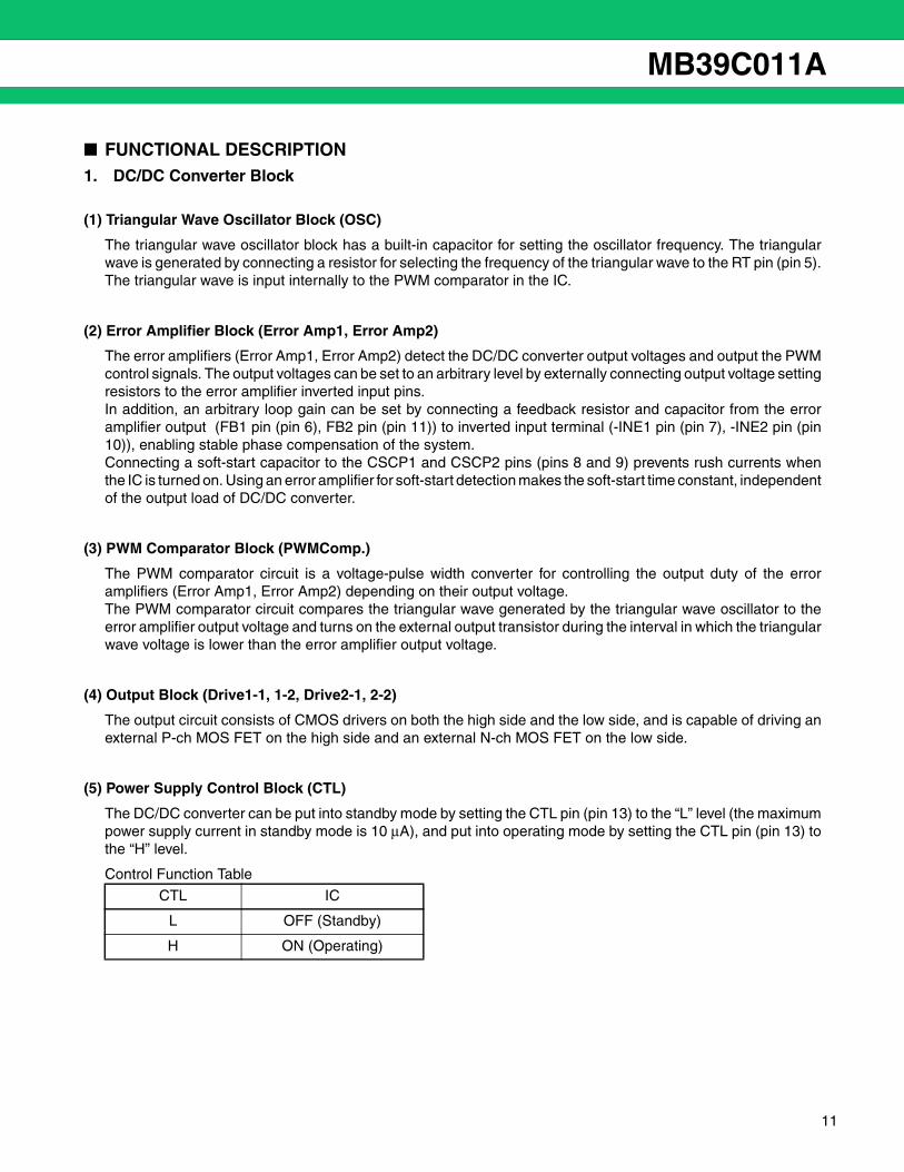
FUNCTIONAL DESCRIPTION1. DC/DC Converter Block
(1) Triangular Wave Oscillator Block (OSC)
The triangular wave oscillator block has a built-in capacitor for setting the oscillator frequency. The triangularwave is generated by connecting a resistor for selecting the frequency of the triangular wave to the RT pin (pin 5).The triangular wave is input internally to the PWM comparator in the IC.
(2) Error Amplifier Block (Error Amp1, Error Amp2)
The error amplifiers (Error Amp1, Error Amp2) detect the DC/DC converter output voltages and output the PWMcontrol signals. The output voltages can be set to an arbitrary level by externally connecting output voltage settingresistors to the error amplifier inverted input pins.In addition, an arbitrary loop gain can be set by connecting a feedback resistor and capacitor from the erroramplifier output (FB1 pin (pin 6), FB2 pin (pin 11)) to inverted input terminal (-INE1 pin (pin 7), -INE2 pin (pin10)), enabling stable phase compensation of the system.Connecting a soft-start capacitor to the CSCP1 and CSCP2 pins (pins 8 and 9) prevents rush currents whenthe IC is turned on. Using an error amplifier for soft-start detection makes the soft-start time constant, independentof the output load of DC/DC converter.
(3) PWM Comparator Block (PWMComp.)
The PWM comparator circuit is a voltage-pulse width converter for controlling the output duty of the erroramplifiers (Error Amp1, Error Amp2) depending on their output voltage.The PWM comparator circuit compares the triangular wave generated by the triangular wave oscillator to theerror amplifier output voltage and turns on the external output transistor during the interval in which the triangularwave voltage is lower than the error amplifier output voltage.
(4) Output Block (Drive1-1, 1-2, Drive2-1, 2-2)
The output circuit consists of CMOS drivers on both the high side and the low side, and is capable of driving anexternal P-ch MOS FET on the high side and an external N-ch MOS FET on the low side.
(5) Power Supply Control Block (CTL)
The DC/DC converter can be put into standby mode by setting the CTL pin (pin 13) to the “L” level (the maximumpower supply current in standby mode is 10 µA), and put into operating mode by setting the CTL pin (pin 13) tothe “H” level.
Control Function Table
CTL IC
L OFF (Standby)
H ON (Operating)
11
MB39C011A
12
2. Protection Function
(1) Soft-start Circuit
To prevent rush currents when the IC is turned on, soft-start can be performed by connecting soft-start capacitors(CSCP1 and CSCP2) to the CSCP1 and CSCP2 pins (pins 8 and 9). When CTL pin (pin 13) is driven to the “H”level and the IC begins operation (VCC ≥ UVLO threshold voltage), the external soft-start capacitors (CSCP1and CSCP2) connected to the CSCP1 and CSCP2 pins (pins 8 and 9) are charged by the charging currentobtained from the following formula.
ICS ≅ 5.4 × 10⁻⁵ / RT
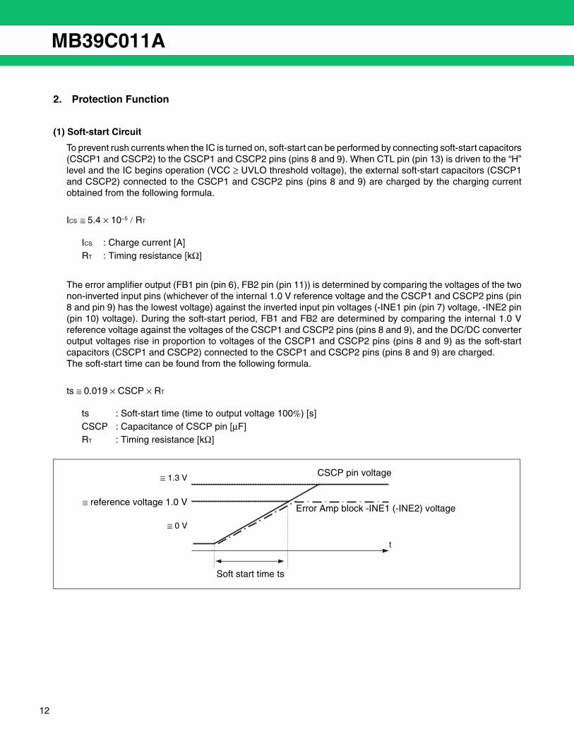
The error amplifier output (FB1 pin (pin 6), FB2 pin (pin 11)) is determined by comparing the voltages of the twonon-inverted input pins (whichever of the internal 1.0 V reference voltage and the CSCP1 and CSCP2 pins (pin8 and pin 9) has the lowest voltage) against the inverted input pin voltages (-INE1 pin (pin 7) voltage, -INE2 pin(pin 10) voltage). During the soft-start period, FB1 and FB2 are determined by comparing the internal 1.0 Vreference voltage against the voltages of the CSCP1 and CSCP2 pins (pins 8 and 9), and the DC/DC converteroutput voltages rise in proportion to voltages of the CSCP1 and CSCP2 pins (pins 8 and 9) as the soft-startcapacitors (CSCP1 and CSCP2) connected to the CSCP1 and CSCP2 pins (pins 8 and 9) are charged.The soft-start time can be found from the following formula.
ts ≅ 0.019 × CSCP × RT
ICS : Charge current [A]RT : Timing resistance [kΩ]
ts : Soft-start time (time to output voltage 100%) [s]CSCP : Capacitance of CSCP pin [µF]RT : Timing resistance [kΩ]
t
≅ reference voltage 1.0 VError Amp block -INE1 (-INE2) voltage
CSCP pin voltage
Soft start time ts
≅ 1.3 V
≅ 0 V

MB39C011A
• Soft-start circuit
Error Amp
(1.0 V)
-INE1
CSCP1
R1
R2
VB
Ic1 Ic2Vo
FB1
UVLO
7
8
6
CSCP
10(-INE2)
(FB2) 11
9(CSCP2)
Ics
RT : Timing resistor
Ic1[A] ≅ 3.7 × 10⁻⁵/RT [kΩ]Ic2[A] ≅ 1.7 × 10⁻⁵/RT [kΩ]
L priority
13
MB39C011A
14
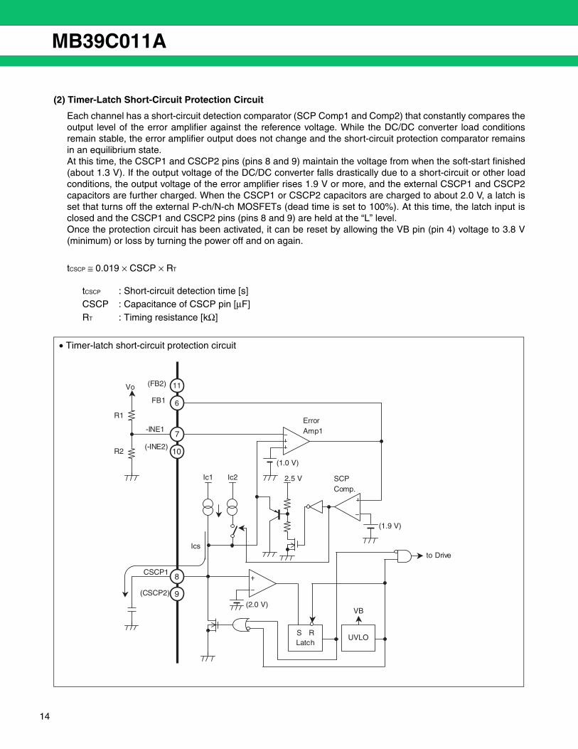
(2) Timer-Latch Short-Circuit Protection Circuit
Each channel has a short-circuit detection comparator (SCP Comp1 and Comp2) that constantly compares theoutput level of the error amplifier against the reference voltage. While the DC/DC converter load conditionsremain stable, the error amplifier output does not change and the short-circuit protection comparator remainsin an equilibrium state. At this time, the CSCP1 and CSCP2 pins (pins 8 and 9) maintain the voltage from when the soft-start finished(about 1.3 V). If the output voltage of the DC/DC converter falls drastically due to a short-circuit or other loadconditions, the output voltage of the error amplifier rises 1.9 V or more, and the external CSCP1 and CSCP2capacitors are further charged. When the CSCP1 or CSCP2 capacitors are charged to about 2.0 V, a latch isset that turns off the external P-ch/N-ch MOSFETs (dead time is set to 100%). At this time, the latch input isclosed and the CSCP1 and CSCP2 pins (pins 8 and 9) are held at the “L” level. Once the protection circuit has been activated, it can be reset by allowing the VB pin (pin 4) voltage to 3.8 V(minimum) or loss by turning the power off and on again.
tCSCP ≅ 0.019 × CSCP × RT
tCSCP : Short-circuit detection time [s]CSCP : Capacitance of CSCP pin [µF]RT : Timing resistance [kΩ]
• Timer-latch short-circuit protection circuit
(1.9 V)
Ic1 Ic2
UVLO
CSCP1
S RLatch
SCPComp.
VB
Vo
R1
R2
ErrorAmp1
(1.0 V)
-INE1
FB1
to Drive
(2.0 V)
2.5 V
(-INE2)
6
7
10
(FB2) 11
8
9(CSCP2)
Ics
MB39C011A
(1) When the CTL pin (pin 13) is set to the “H” level and the IC becomes active, the voltages of the CSCP1 andCSCP2 pins (pins 8 and 9) rise due to the capacitors attached externally to the CSCP1 and CSCP2 pins(pins 8 and 9) being charged. During this time, Error Amp1 and Error Amp2 are controlled by the CSCP1and CSCP2 pins (pins 8 and 9) and the -INE1 and -INE2 pins (pins 7 and 10) inputs, thus performing a soft-start.
(2) When the CSCP1 and CSCP2 pins (pins 8 and 9) reach 1 V or more, Error Amp1 and Error Amp2 becomecontrolled by the internal reference voltage (1 V) and the -INE1 and -INE2 pin (pins 7 and 10) inputs, andthe output voltage is held at a constant level.
(3) The CSCP1 and CSCP2 pins (pins 8 and 9) are clamped to about 1.3 V.
(4) When there is a short circuit in the load and the error amplifier output becomes 1.9 V or more, the short-circuit protection comparator (SCP Comp.) is activated and the CSCP1 and CSCP2 capacitors are chargedfurther.
(5) If the short-circuit in the load is cleared within the short-circuit detection time tCSCP, the CSCP1 and CSCP2pins (pins 8 and 9) return to the clamping voltage of about 1.3 V.
(6) When there is a short-circuit in the load and the error amplifier output becomes 1.9 V or more, the short-circuit protection comparator (SCP Comp.) is activated and the CSCP1 and CSCP2 capacitors are chargedfurther.
(7) The latch is set when the load short-circuit is not released even if short-circuit detection time tCSCP passes,external MOS FET P-ch/N-ch are turned off, and the CSCP1,CSCP2 pins (pins 8 and 9) are hold at “L” level.
• Soft-start and short-circuit protection timing chart
(1) (2) (3) (4) (5) (6) (7)
t
ts
2.0 V
1.3 V
1.0 V
tcscp
CSCP voltage Soft-start time Short-circuit detection time
Output short Output short
15

MB39C011A
16
Notes : • The output is stopped by the short-circuit protection (SCP) function when the DC/DC output is short-circuited to GND etc. However, care needs to be taken because the short-circuit protection (SCP) function will not stop the output when a half short-circuit occurs. Measures such as placing a fuse in the input can be used for this situation. [ Half short-circuit refers to a short-circuit condition where an overcurrent flows, but it is not sufficient to reduce the output voltage.]
• In the event that an output short current flows that exceeds the capacity of the input power supply, the power supply voltage may drop. If the power supply voltage at this time drops below 3.8 V, the output is stopped by the under voltage lockout protection circuit (UVLO). However, once the input power supply voltage recovers after the output has been stopped, the output will begin again. Care needs to be taken because this situation may result in a repeating cycle of “short-circuit → power-supply voltage drop → output stop → power-supply voltage recovery → output start → short-circuit”. There are putting a fuse in the input etc. as measures.
• Notes the short-circuit protection (SCP) function when the DC/DC converter is started/stopped. The output may also be stopped by the short-circuit protection (SCP) function under the following conditions. • Operations that act on the input power supply and the CTL pin (for example, shorting the input power
supply to the CTL pin).• During the transition period when the input power supply voltage (VIN) is changing (such as when the
input power supply is turned on or turned off), the condition is met that input power supply voltage (VIN) < output setting voltage (VO).
Although this is normal IC operation, as an example of startup of the IC, the output may be stopped due to the following process. (1) DC/DC converter output begins when VIN ( = VB) > UVLO threshold voltage.(2) A period of time occurs where the input power supply voltage (VIN) < the output voltage setting (VO),
and the duty cycle becomes 100% on. The error amplifier output rises above 1.9 V due to the feedback control.
(3) The output is stopped after the short-circuit detection time has elapsed.
MB39C011A
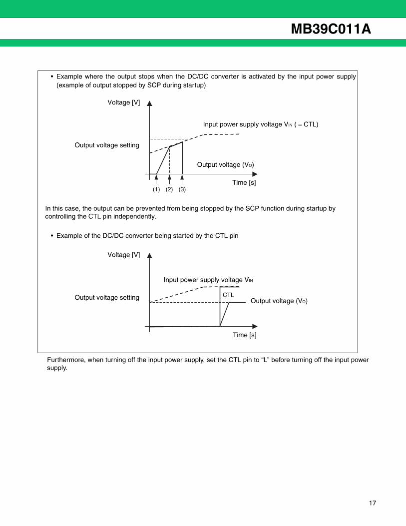
Furthermore, when turning off the input power supply, set the CTL pin to “L” before turning off the input powersupply.
• Example where the output stops when the DC/DC converter is activated by the input power supply(example of output stopped by SCP during startup)
In this case, the output can be prevented from being stopped by the SCP function during startup by controlling the CTL pin independently.
• Example of the DC/DC converter being started by the CTL pin
(1) (2) (3)
Output voltage setting
Time [s]
Output voltage (VO)
Input power supply voltage VIN ( = CTL)
Voltage [V]
CTLOutput voltage setting
Time [s]
Output voltage (VO)
Input power supply voltage VIN
Voltage [V]
17
MB39C011A
18
(3) Under Voltage Lockout Protection Circuit (UVLO)
A drop in the power supply voltage may cause the IC to malfunction, resulting in breakdown or degradation ofthe system. To prevent such malfunctions, the under voltage lockout protection circuit detects decreases in VBvoltage due to the power supply voltage, and locks, the OUT1-1 pin (pin 2) and OUT2-1 pin (pin 15) at the “H”level and the OUT1-2 pin (pin 3) and OUT2-2 pin (pin 14) at the “L” level. The system is restored if the VB voltagerises above the threshold voltage of the under voltage lockout protection circuit.
Function Table When the Protection Circuit (UVLO) is OperatingWhen the UVLO circuit is operating (the VB voltage is below the UVLO threshold voltage), the following pinsare fixed at the following logic levels.
(4) Operation When CTL is Turned On and Off
When CTL is turned on, the internal reference voltages VR1 and VB begin to rise. When VB exceeds the thresholdvoltage (VTH) of UVLO (under voltage lockout protection circuit), UVLO is released, and the output drive circuitsof each channel are allowed to operate.When CTL is off, the output drive circuit of each channel is locked in the full off state and the CSCP1 and CSCP2pins (pins 8 and 9) are fixed at the “L” level, even if the UVLO circuit is in the clear state. When the internalreference voltages VR1 and VB begin to fall and when VB falls below the threshold voltage of the UVLO (undervoltage lockout protection circuit), the UVLO circuit is activated.
(5) Independent Control Of Each Channel
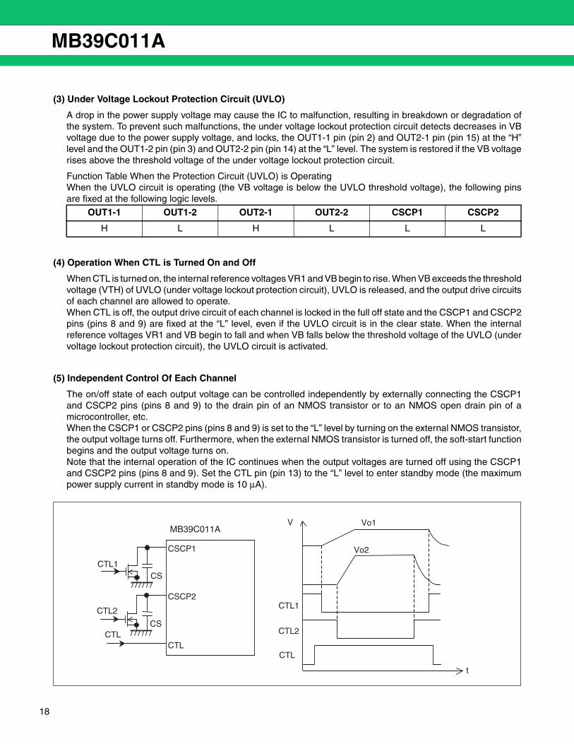
The on/off state of each output voltage can be controlled independently by externally connecting the CSCP1and CSCP2 pins (pins 8 and 9) to the drain pin of an NMOS transistor or to an NMOS open drain pin of amicrocontroller, etc. When the CSCP1 or CSCP2 pins (pins 8 and 9) is set to the “L” level by turning on the external NMOS transistor,the output voltage turns off. Furthermore, when the external NMOS transistor is turned off, the soft-start functionbegins and the output voltage turns on. Note that the internal operation of the IC continues when the output voltages are turned off using the CSCP1and CSCP2 pins (pins 8 and 9). Set the CTL pin (pin 13) to the “L” level to enter standby mode (the maximumpower supply current in standby mode is 10 µA).
OUT1-1 OUT1-2 OUT2-1 OUT2-2 CSCP1 CSCP2
H L H L L L
CTL
V
t
Vo1
Vo2
CTL1
CTL2
MB39C011A
CTL
CS CTL1
CS CTL2
CSCP1
CTL
CSCP2
MB39C011A
SWITCHING SCHEME SELECTIONThis device can operate even by a synchronous rectification and an asynchronous rectification. There is supe-riority or inferiority respectively. Select the switching type considering the features as a guide.
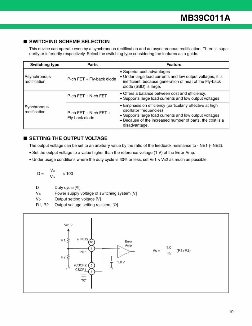
SETTING THE OUTPUT VOLTAGEThe output voltage can be set to an arbitrary value by the ratio of the feedback resistance to -INE1 (-INE2).
• Set the output voltage to a value higher than the reference voltage (1 V) of the Error Amp.
• Under usage conditions where the duty cycle is 30% or less, set VO1 < VO2 as much as possible.
Switching type Parts Feature
Asynchronous rectification
P-ch FET + Fly-back diode
• Superior cost advantages• Under large load currents and low output voltages, it is
inefficient because generation of heat of the Fly-back diode (SBD) is large.
Synchronous rectification
P-ch FET + N-ch FET• Offers a balance between cost and efficiency.• Supports large load currents and low output voltages
P-ch FET + N-ch FET + Fly-back diode
• Emphasis on efficiency (particularly effective at high oscillator frequencies)
• Supports large load currents and low output voltages• Because of the increased number of parts, the cost is a
disadvantage.
D =VO
× 100VIN
D : Duty cycle [%]VIN : Power supply voltage of switching system [V]VO : Output setting voltage [V]R1, R2 : Output voltage setting resistors [Ω]
R1
R2
Vo (R1+R2)=R2
1.0
Vo1,2
CSCP1(CSCP2)
-INE1
(-INE2)10
7
9
8
1.0 V
ErrorAmp
19
MB39C011A
20
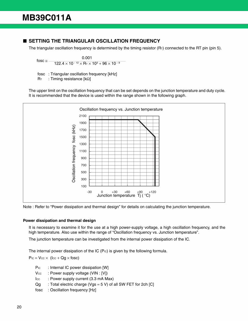
SETTING THE TRIANGULAR OSCILLATION FREQUENCYThe triangular oscillation frequency is determined by the timing resistor (RT) connected to the RT pin (pin 5).
fosc : Triangular oscillation frequency [kHz]RT : Timing resistance [kΩ]
The upper limit on the oscillation frequency that can be set depends on the junction temperature and duty cycle.It is recommended that the device is used within the range shown in the following graph.
Note : Refer to “Power dissipation and thermal design” for details on calculating the junction temperature.
Power dissipation and thermal design
It is necessary to examine it for the use at a high power-supply voltage, a high oscillation frequency, and thehigh temperature. Also use within the range of “Oscillation frequency vs. Junction temperature”.
The junction temperature can be investigated from the internal power dissipation of the IC.
The internal power dissipation of the IC (PIC) is given by the following formula.
PIC = VCC × (ICC + Qg × fosc)
fosc ≅0.001
122.4 × 10 − 12 × RT × 103 + 96 × 10 − 9
PIC : Internal IC power dissipation [W]VCC : Power supply voltage (VIN : [V]) ICC : Power supply current (3.3 mA Max)Qg : Total electric charge (Vgs = 5 V) of all SW FET for 2ch [C]fosc : Oscillation frequency [Hz]
2100
1900
1700
1500
1300
1100
900
700
500
300
100
-30 0 +30 +60 +90 +120
Osc
illat
ion
freq
uenc
y fo
sc (
kHz)
Oscillation frequency vs. Junction temperature
Junction temperature Tj ( °C)
MB39C011A
The junction temperature is given by the following formula.
Tj = Ta + θja × PIC
Tj : Junction temperature ( + 125 °C Max)Ta : Ambient temperature [ °C]θja : TSSOP-16 package thermal resistance (94 °C/W)PIC : Internal IC power dissipation [W]
21
MB39C011A
22
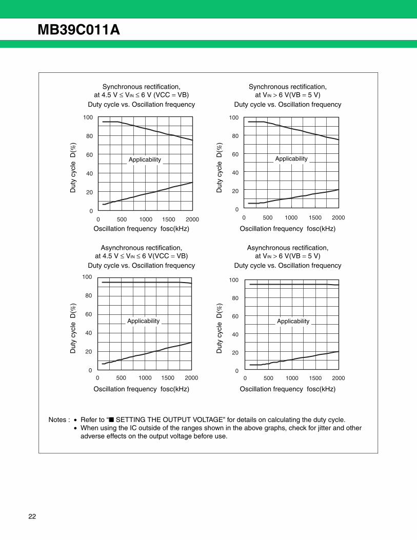
Notes : • Refer to “ SETTING THE OUTPUT VOLTAGE” for details on calculating the duty cycle.• When using the IC outside of the ranges shown in the above graphs, check for jitter and other
adverse effects on the output voltage before use.
Synchronous rectification, at 4.5 V ≤ VIN ≤ 6 V (VCC = VB)
Synchronous rectification, at VIN > 6 V(VB = 5 V)
Duty cycle vs. Oscillation frequency Duty cycle vs. Oscillation frequency
Dut
y cy
cle
D(%
)
Dut
y cy
cle
D(%
)Oscillation frequency fosc(kHz) Oscillation frequency fosc(kHz)
Asynchronous rectification, at 4.5 V ≤ VIN ≤ 6 V(VCC = VB)
Asynchronous rectification, at VIN > 6 V(VB = 5 V)
Duty cycle vs. Oscillation frequency Duty cycle vs. Oscillation frequency
Dut
y cy
cle
D(%
)
Dut
y cy
cle
D(%
)
Oscillation frequency fosc(kHz) Oscillation frequency fosc(kHz)
100
80
60
40
20
00 500 1000 1500 2000
Applicability
100
80
60
40
20
00 500 1000 1500 2000
Applicability
100
80
60
40
20
00 500 1000 1500 2000
Applicability
100
80
60
40
20
00 500 1000 1500 2000
Applicability
MB39C011A
SETTING THE SOFT-START AND SHORT-CIRCUIT DETECTION TIMESSet the soft-start time and the short-circuit detection time using the CSCP pins. Both become the same time.
ts = tCSCP ≅ 0.019 × CSCP × RT
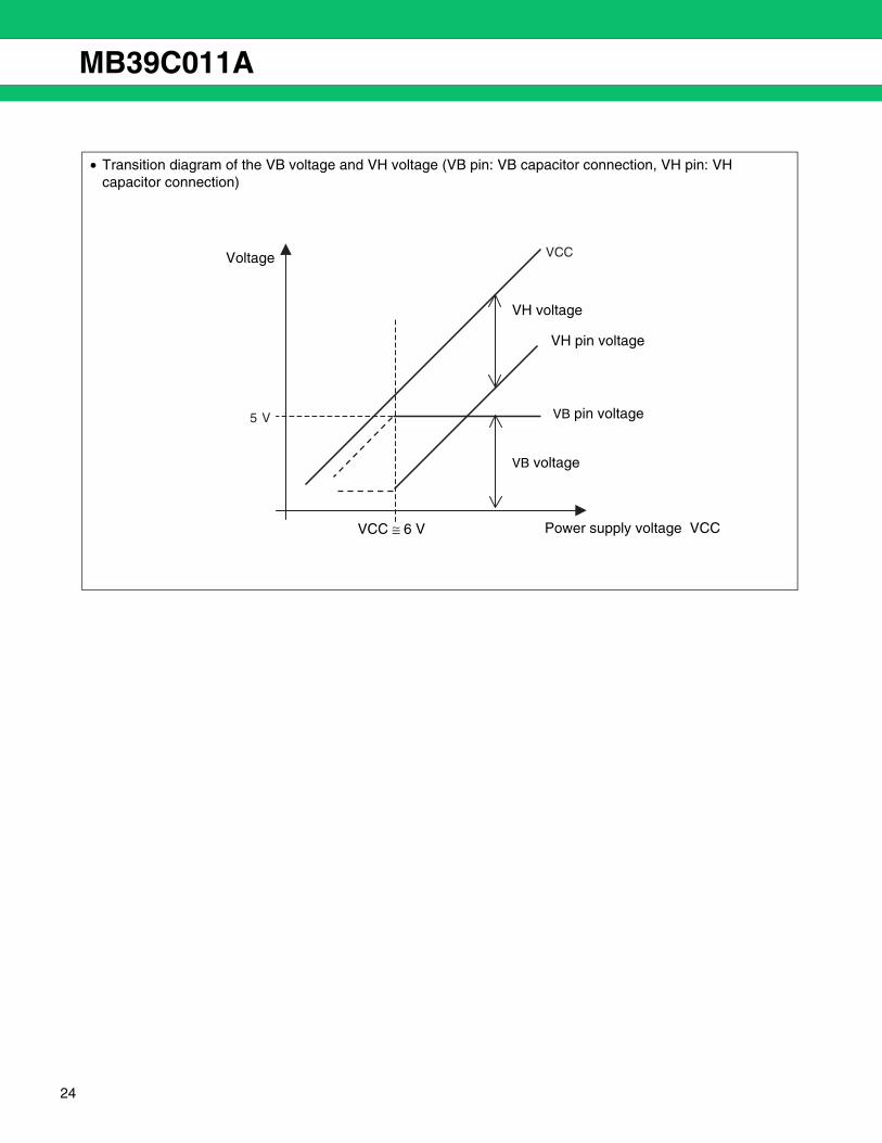
VB PIN AND VH PIN CONNECTIONS IN CONDITION OF VCC VOLTAGEIn the range of 4.5 V ≤ VCC ≤ 6.0 V, there is a chance that the VB voltage*1 and VH voltage*2 may drop due tothe internal IC regulator saturating. As a result, there are drive voltage shortage and a bird clapper of SW FET. It is therefore recommended that the VB pin (pin 4) and VH pin (pin 16) are connected as shown in the “VB pinand VH pin connection table”.
*1 : Voltage between VB pin (pin 4) and GND pin (pin 12) : 5 V
*2 : Voltage between VCC pin (pin 1) and VH pin (pin 16) : 5 V
• VB pin and VH pin connection table
*3 : Check that the switching operation is functioning normally.
*4 : Refer to the connection of the VB pin (pin 4) and the VH pin (pin 16) in the “ BLOCK DIAGRAM”.
ts : Soft-start time (time to output voltage 100%) [s]tCSCP : Short-circuit detection time [s]CSCP : CSCP pin capacitor [µF]RT : Timing resistance [kΩ]
VCC condition VB pin VH pin
4.5 ≤ VCC ≤ 6 V Connected to VCC Connected to GND
6 V ≤ VCC ≤ 17 V VB capacitor connection*4 VH capacitor connection*4
Used with VCC crossing 6 V*3
(ex. 5 V ≤ VCC ≤ 7 V)VB capacitor connection*4 VH capacitor connection*4
23
MB39C011A
24
• Transition diagram of the VB voltage and VH voltage (VB pin: VB capacitor connection, VH pin: VH capacitor connection)
5 V
VCCVoltage
VB voltage
VB pin voltage
VH pin voltage
VH voltage
Power supply voltage VCCVCC ≅ 6 V
MB39C011A
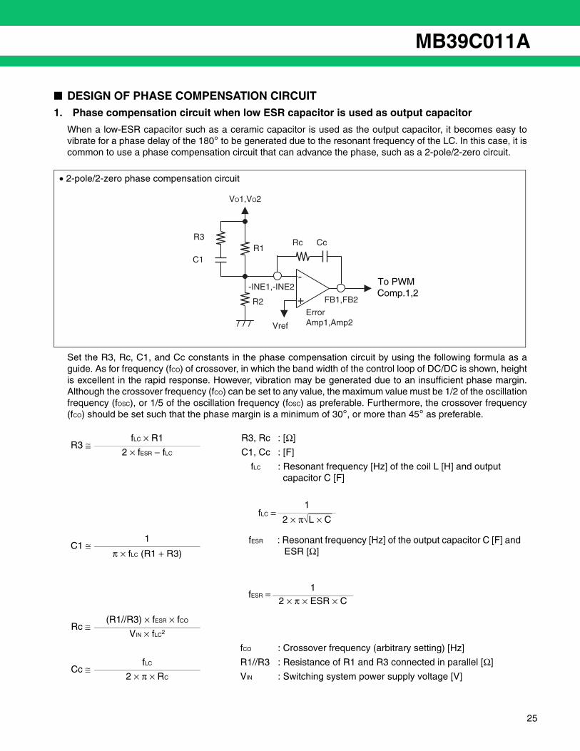
DESIGN OF PHASE COMPENSATION CIRCUIT1. Phase compensation circuit when low ESR capacitor is used as output capacitor
When a low-ESR capacitor such as a ceramic capacitor is used as the output capacitor, it becomes easy tovibrate for a phase delay of the 180° to be generated due to the resonant frequency of the LC. In this case, it iscommon to use a phase compensation circuit that can advance the phase, such as a 2-pole/2-zero circuit.
Set the R3, Rc, C1, and Cc constants in the phase compensation circuit by using the following formula as aguide. As for frequency (fCO) of crossover, in which the band width of the control loop of DC/DC is shown, heightis excellent in the rapid response. However, vibration may be generated due to an insufficient phase margin.Although the crossover frequency (fCO) can be set to any value, the maximum value must be 1/2 of the oscillationfrequency (fOSC), or 1/5 of the oscillation frequency (fOSC) as preferable. Furthermore, the crossover frequency(fCO) should be set such that the phase margin is a minimum of 30°, or more than 45° as preferable.
R3 ≅fLC × R1 R3, Rc : [Ω]
2 × fESR − fLC C1, Cc : [F]
fLC : Resonant frequency [Hz] of the coil L [H] and output capacitor C [F]
C1 ≅1 fESR : Resonant frequency [Hz] of the output capacitor C [F] and
ESR [Ω] π × fLC (R1 + R3)
Rc ≅(R1//R3) × fESR × fCO
VIN × fLC2
fCO : Crossover frequency (arbitrary setting) [Hz]
Cc ≅fLC R1//R3 : Resistance of R1 and R3 connected in parallel [Ω]
2 × π × RC VIN : Switching system power supply voltage [V]
• 2-pole/2-zero phase compensation circuit
VO1,VO2
FB1,FB2
Error Amp1,Amp2 Vref
-
+R2
-INE1,-INE2
R3Rc Cc
R1C1
To PWMComp.1,2
fLC =1
2 × π√L × C
fESR =1
2 × π × ESR × C
25
MB39C011A
26
2. Notes on phase compensation circuit constants
Select the constants of the following three points and select the constant for the design of the phase compensationcircuit when the large load sudden change, or the capacitor is connected to DC/DC converter operating. In particular, if a capacitance much larger than the output capacitance of the DC/DC converter is connected byhard-switching while the DC/DC converter is operating, the output voltage may begin vibrating or the protectionfunction may be activated, due to the sudden response. Note the following points.
(1) Error Amp output (FB1 and FB2 pins) current capacity
The resistance constants of the phase compensation circuit need to be designed by considering the currentcapacities of the Error Amp outputs (FB1 and FB2 pins (pins 6 and 11)). Take the output source current ( − 300 µA Max) of the Error Amp and the threshold voltage VT100 (1.7 V Typ) of the PWM Comp into consideration,select the resistance values such that the following formula is satisfied.
Although low resistance values may be desired to improve the noise immunity, the above formula may not besatisfied as a result. While it is ideal for each of the resistance values to satisfy the above formula, in this situationthe values may be used after confirming that there are no problems when used under the rapidly varying loadconditions.
(2) Phase margin at the output load changes
Select phase compensation constants that ensure the phase margin when the output load (resistive load,capacitative load, inductive load) is connected.
(3) Phase margin at the reverse current flow from the output pin
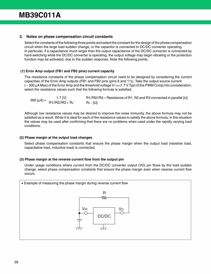
Under usage conditions where current from the DC/DC converter output (VO) pin flows by the load suddenchange, select phase compensation constants that ensure the phase margin even when reverse current flowoccurs.
300 [µA] >1.7 [V] R1//R2//R3 = Resistance of R1, R2 and R3 connected in parallel [Ω]
R1//R2//R3 + RC RC : [Ω]
• Example of measuring the phase margin during reverse current flow
R
DC/DC
VIN VO
MB39C011A
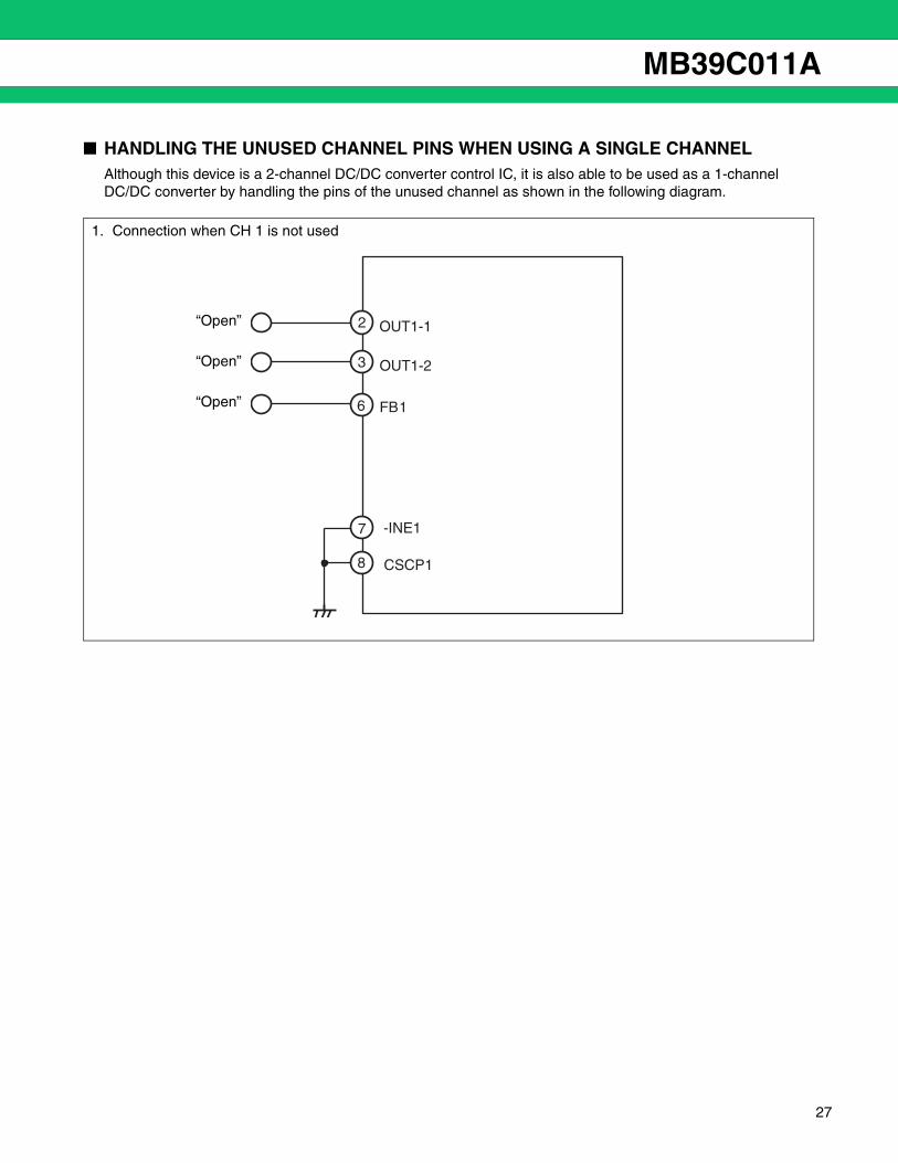
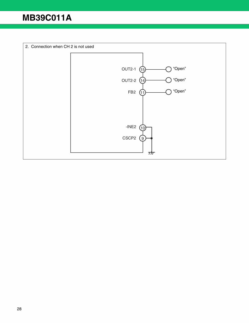
HANDLING THE UNUSED CHANNEL PINS WHEN USING A SINGLE CHANNELAlthough this device is a 2-channel DC/DC converter control IC, it is also able to be used as a 1-channel DC/DC converter by handling the pins of the unused channel as shown in the following diagram.
1. Connection when CH 1 is not used
OUT1-2
CSCP18
3
FB1
-INE1
6
7
2 OUT1-1“Open”
“Open”
“Open”
27
MB39C011A
28
2. Connection when CH 2 is not used
-INE2
CSCP2
15OUT2-1
FB2
OUT2-2
14
11
10
9
“Open”
“Open”
“Open”
MB39C011A
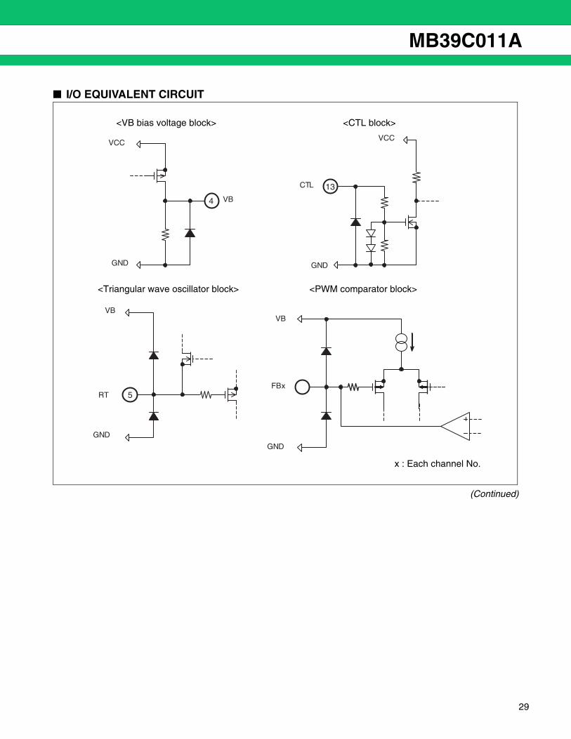
I/O EQUIVALENT CIRCUIT
(Continued)
GND
CTL
VCC
VB
GND
VCC
RT
VB
GND
VB
FBx
GND
4
13
5
x : Each channel No.
<Triangular wave oscillator block> <PWM comparator block>
<VB bias voltage block> <CTL block>
29
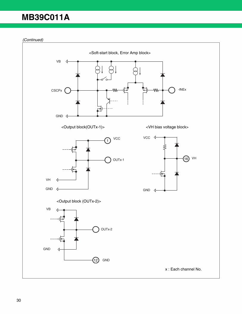
MB39C011A
30
(Continued)
VB
CSCPx
GND
-INEx
VH
GND
VCC
VH
OUTx-1
VCC
GND
OUTx-2
VB
GND
GND
1
16
12
x : Each channel No.
<Output block (OUTx-2)>
<VH bias voltage block><Output block(OUTx-1)>
<Soft-start block, Error Amp block>
MB39C011A
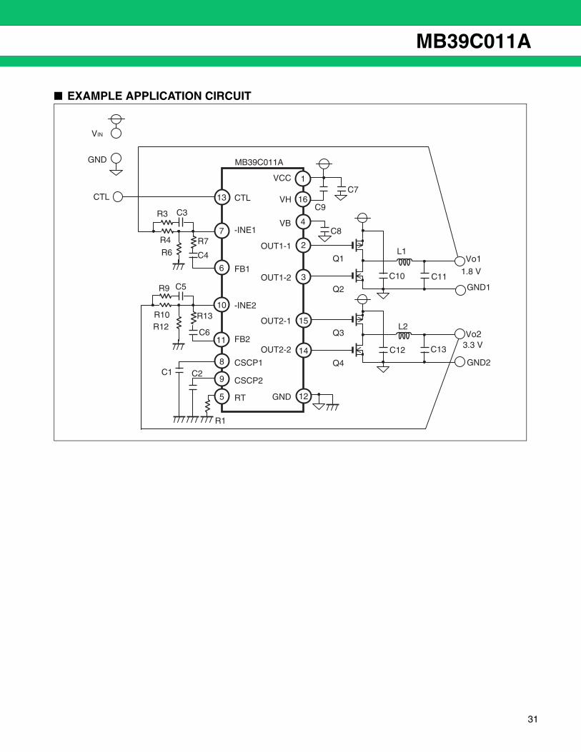
EXAMPLE APPLICATION CIRCUIT
R9 C5
R12 R13
C6
R10
R7
C4
R3 C3
R6
R4
GND
VIN
Vo1
GND1
VCC
OUT1-1
OUT1-2
VH
VB
CSCP1
CSCP2
OUT2-1
OUT2-2
Vo2
GND2
FB2
FB1
-INE2
-INE1
CTL
RT
R1
Q1
Q2
Q3
Q4
L1
L2
C11
C13
C2 C1
C7
C8
C9
GND
C10
C12
2
3
4
9
8 14
15
7
6
10
11
13
5
16
1
MB39C011A
CTL
1.8 V
3.3 V
12
31
MB39C011A
32
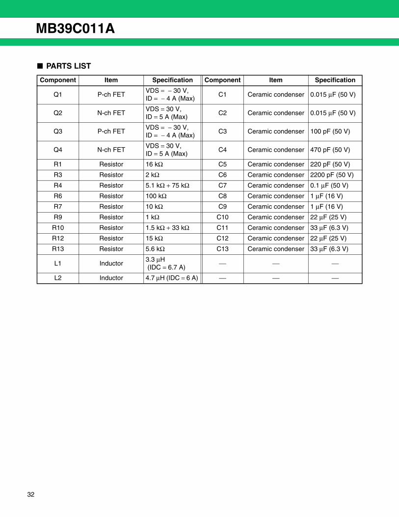
PARTS LIST
Component Item Specification Component Item Specification
Q1 P-ch FETVDS = − 30 V, ID = − 4 A (Max)
C1 Ceramic condenser 0.015 µF (50 V)
Q2 N-ch FETVDS = 30 V, ID = 5 A (Max)
C2 Ceramic condenser 0.015 µF (50 V)
Q3 P-ch FETVDS = − 30 V, ID = − 4 A (Max)
C3 Ceramic condenser 100 pF (50 V)
Q4 N-ch FETVDS = 30 V, ID = 5 A (Max)
C4 Ceramic condenser 470 pF (50 V)
R1 Resistor 16 kΩ C5 Ceramic condenser 220 pF (50 V)
R3 Resistor 2 kΩ C6 Ceramic condenser 2200 pF (50 V)
R4 Resistor 5.1 kΩ + 75 kΩ C7 Ceramic condenser 0.1 µF (50 V)
R6 Resistor 100 kΩ C8 Ceramic condenser 1 µF (16 V)
R7 Resistor 10 kΩ C9 Ceramic condenser 1 µF (16 V)
R9 Resistor 1 kΩ C10 Ceramic condenser 22 µF (25 V)
R10 Resistor 1.5 kΩ + 33 kΩ C11 Ceramic condenser 33 µF (6.3 V)
R12 Resistor 15 kΩ C12 Ceramic condenser 22 µF (25 V)
R13 Resistor 5.6 kΩ C13 Ceramic condenser 33 µF (6.3 V)
L1 Inductor3.3 µH (IDC = 6.7 A)
⎯ ⎯ ⎯
L2 Inductor 4.7 µH (IDC = 6 A) ⎯ ⎯ ⎯
MB39C011A
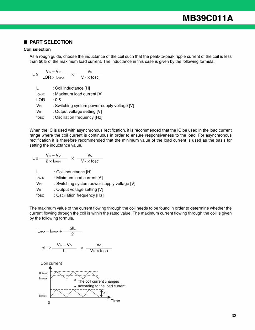
PART SELECTIONCoil selection
As a rough guide, choose the inductance of the coil such that the peak-to-peak ripple current of the coil is lessthan 50% of the maximum load current. The inductance in this case is given by the following formula.
When the IC is used with asynchronous rectification, it is recommended that the IC be used in the load currentrange where the coil current is continuous in order to ensure responsiveness to the load. For asynchronousrectification it is therefore recommended that the minimum value of the load current is used as the basis forsetting the inductance value.
The maximum value of the current flowing through the coil needs to be found in order to determine whether thecurrent flowing through the coil is within the rated value. The maximum current flowing through the coil is givenby the following formula.
L ≥VIN − VO
× VO
LOR × IOMAX VIN × fosc
L : Coil inductance [H]IOMAX : Maximum load current [A]LOR : 0.5VIN : Switching system power-supply voltage [V]VO : Output voltage setting [V]fosc : Oscillation frequency [Hz]
L ≥VIN − VO
× VO
2 × IOMIN VIN × fosc
L : Coil inductance [H]IOMIN : Minimum load current [A]VIN : Switching system power-supply voltage [V]VO : Output voltage setting [V]fosc : Oscillation frequency [Hz]
ILMAX = IOMAX +∆IL2
∆IL ≥VIN − VO
× VO
L VIN × fosc
∆IL
ILMAX
IOMAX
IOMIN
0
The coil current changes according to the load current.
Time
Coil current
33
MB39C011A
34
SW FET selection
The maximum value of the current flowing through the SW FET needs to be found in order to determine whetherthe current flowing through the SW FET is within the rated value. The maximum current flowing through the SW FET is given by the following formula.
Furthermore, the power dissipation of the SW FET needs to be found in order to determine whether the powerdissipation of the SW FET is within the rated value. The power dissipation of the SW FET is given by the followingformula.
High side FET (P-ch MOS FET) power dissipation PHiSideFET = PRon + PSW
ILMAX : Maximum coil current [A]IOMAX : Maximum load current [A]∆IL : Coil ripple current peak to peak value [A]L : Coil inductance [H]VIN : Switching system power-supply voltage [V]VO : Output setting voltage [V]fosc : Oscillation frequency [Hz]
IDMAX ≥ IOMAX +∆IL2
IDMAX : Maximum SW FET drain current [A]IOMAX : Maximum load current [A]∆IL : Coil ripple current peak to peak value [A]
PRon : High side FET (P-ch MOS FET) conduction loss PRon = IOMAX2 ×VO
× RonVIN
IOMAX : Maximum load current [A]VIN : Switching system power supply voltage [V]VO : Output voltage [V]Ron : High side FET ON resistance [Ω]
PSW : High side FET (P-ch MOS FET) switching loss PSW =VIN × fOSC (Ibtm × tr × Itop × tf)
2
VIN : Switching system power supply voltage [V]fosc : Oscillation frequency [Hz]Ibtm : Bottom value of ripple current of coil [A]
Ibtm = IOMAX −∆IL2
Itop : Top value of ripple current of coil [A]
MB39C011A
tr and tf are simply obtained by the following formula.
To select SW FETs that offer good conversion efficiency, the High side FET in particular should select such thatthe switching loss is small (the power dissipated when the SW FET changes between ON and OFF). However,because there is generally a trade-off between switching loss and conduction loss, this balance needs to beconsidered when making the selection. As a guide, select FETs such that the total Qg of the SW FETs is as follows.
The SW FETs used with this device typically have a drive voltage of 4 V. Although there are FETs that supporta drive voltage of less than 4 V, low drive voltage FETs generally have a larger Qg even at equal value of Ron,the efficiency lowers. If a FET with a low drive voltage is used, check that the low side FET does not self turn-on and that the dead-time is secured under the usage conditions.
Itop = IOMAX +∆IL2
∆IL : Coil ripple current peak to peak value [A]tr : Turn-on time of High side FET [s]tf : Turn-off time of High side FET [s]
tr =Qgd × 4
tf =Qgd × 4
5 − Vgs (on) Vgs (on)
Qgd : Quantity of charge between the gate and drain of High side FET [C]
Vgs(on) : Absolute value of voltage difference between the gate and source of the High side FET at Qgd
[V]
Low side FET(N-ch MOS FET) conduction loss
PLoSideFET = PRon = IOMAX2 × (1 −VO
) × RonVIN
PRon : Low side FET conduction loss [W]IOMAX : Maximum load current [A]VIN : Switching system power supply voltage [V]VO : Output voltage [V]Ron : Low side FET ON resistance [Ω]
QgHiSideFET<0.04
QgLoSideFET<0.04
fosc fosc
QgHiSideFET : Sum total electric charge of the CH1 and CH2 High side FETs [C]QgLoSideFET : Sum total electric charge of the CH1 and CH2 Low side FETs [C]fosc : Oscillation frequency [Hz]
35
MB39C011A
36
Fly-back diode selection
Select a Schottky barrier diode (SBD) that has a small forward voltage drop.
The peak current flowing through the Fly-back diode needs to be found in order to determine whether the currentflowing through the Fly-back diode is within the rated value. When the DC/DC converter IC is used with asyn-chronous rectification, the maximum current through the Fly-back diode is given by the following formula.
Furthermore, the power dissipation of the Fly-back diode needs to be found in order to determine whether thepower dissipation of the Fly-back diode is within the rated value. The power dissipation of the Fly-back diode isgiven by the following formula.
When the DC/DC converter is used with synchronous rectification, the length of time that the current flowsthrough the Fly-back diode is limited to the synchronous rectification period (dead time). For example, at anoscillating frequency of 500 kHz, the proportion of time that current flows is less than 5%. Therefore, select thatFly-back diode current does not exceed the peak forward surge current (IFSM) rated value. The peak forwardsurge current value of the SBD is given by the following formula.
If ≥ IOMAX∆IL2
If : Forward current [A]IOMAX : Maximum load current [A]∆IL : Coil ripple current peak to peak value [A]
PSBD = IOMAX × (1 −VO
) × VfVIN
PSBD : Fly-back diode power dissipation [W]IOMAX : Maximum load current [A]VIN : Switching system power supply voltage [V]VO : Output voltage [V]Vf : Forward voltage [V]
IFSM ≥ IOMAX +∆IL2
IFSM : Peak forward surge current value of Fly-back diode [A]IOMAX : Maximum load current [A]∆IL : Coil ripple current peak to peak value [A]

MB39C011A
Output capacitor selection
Because the ripple voltage increases if the ESR is large, a low ESR capacitor needs to be used in order toreduce the ripple voltage. However, using a capacitor with a low ESR has a large effect on the phase charac-teristics of the loop, and care needs to be taken to prevent the system from losing stability. Furthermore, thecapacitor that is used should have sufficient tolerance for the ripple current.
If taking into account the switching ripple voltage, the minimum necessary capacitance is given by the followingformula.
When a capacitive load is connected, it is recommended that the DC/DC converter output capacitor have thesame capacitance as the load capacitance.
The allowable ripple current of the output capacitor is given by the following formula.
Input capacitor selection
Select an input capacitor that has as small an ESR as possible. Ceramic capacitors are ideal. If a large capac-itance is required that cannot be provided by a ceramic capacitor, use a polymer capacitor or a tantalum capacitorwith a low ESR. Furthermore, the capacitor that is used should have sufficient tolerance for the ripple current.
The allowable ripple current is given by the following formula.
CO ≥1
2π × fosc × (∆VO/∆IL − ESR)
ESR : Series resistance element of output capacitance [Ω]∆VO : Switching ripple voltage [V]∆IL : Coil ripple current peak to peak value [A]CO : Output capacitance [F]fosc : Oscillation frequency [Hz]
Irms ≥∆IL
2√3
Irms : Allowable ripple current (Root-mean-square value) [A]∆IL : Coil ripple current peak to peak value [A]
Irms ≥ IOMAX√VO (VIN − VO)
VIN
Irms : Allowable ripple current (Root-mean-square value) [A]IOMAX : Maximum load current [A]VIN : Switching system power supply voltage [V]VO : Output voltage [V]
37
MB39C011A
38
VB pin capacitor
Although the VB pin capacitor typically has a capacitance of 1 µF, this needs to be adjusted if the SW FET beingused has a large Qg.
The following formula provides a guide to the lower limit of the VB pin capacitor. If this lower limit exceeds 1 µF, use the formula as a guide to set the capacitance.
CVBmin ≥ 0.1 × QgLoSideFET
VH pin capacitor
The VH pin capacitor typically has a capacitance of 1 µF (when the VB pin capacitor ≤ 1 µF). However, thisneeds to be adjusted, if the VB pin capacitor exceeds 1 µF or if the SW FET being used has a large Qg.
The following formula provides a guide to the lower limit of the VH pin capacitor. If this lower limit exceeds 1 µF, use the formula as a guide to set the capacitance.
Large one either of CVHmin ≥ 0.01 × QgHiSideFET or CVHmin ≥ CVB
CVBmin : Lower limit of VB pin capacitor [µF]QgLoSideFET : Sum total electric charge of CH1 and CH2 Low side FETs [nC]
CVHmin : Lower limit of VH pin capacitor [µF]QgHiSideFET : Sum total electric charge of CH1 and CH2 high side FETs [nC]CVB : Capacitance of VB pin capacitor [µF]
MB39C011A
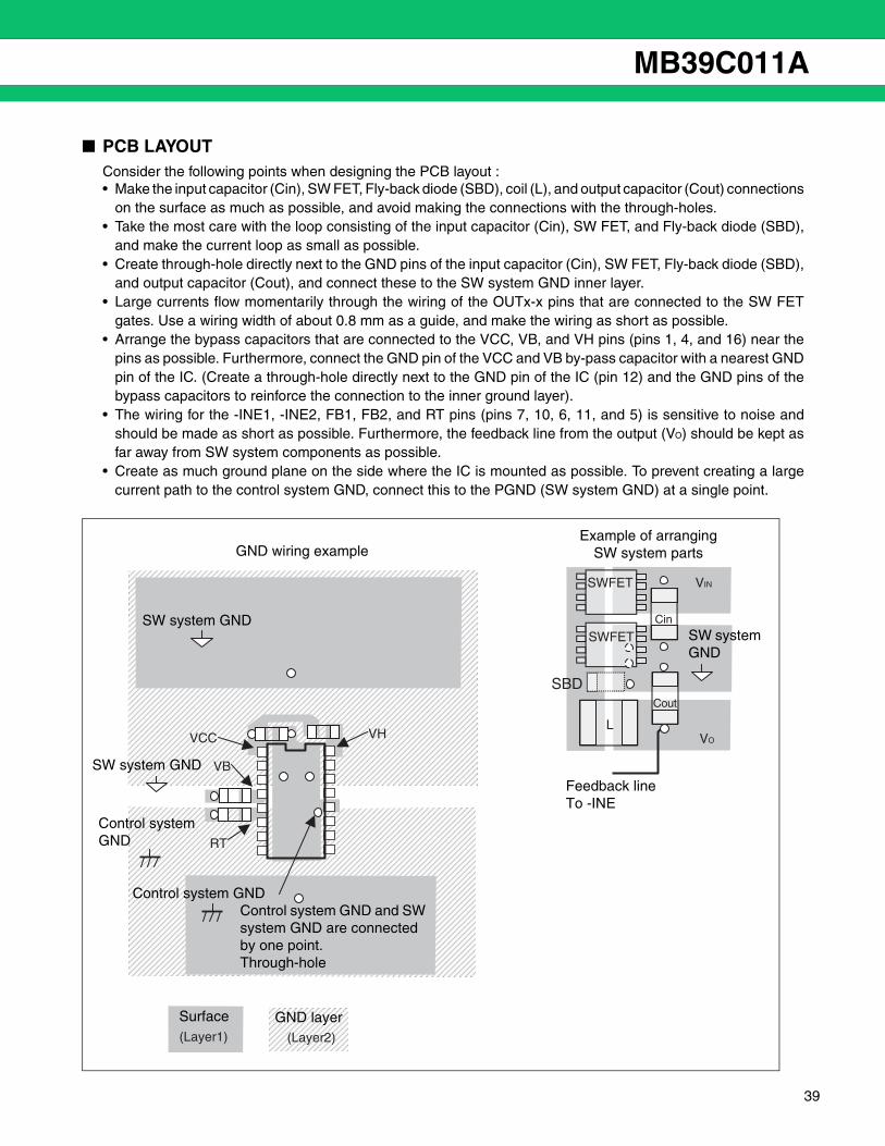
PCB LAYOUTConsider the following points when designing the PCB layout : • Make the input capacitor (Cin), SW FET, Fly-back diode (SBD), coil (L), and output capacitor (Cout) connections
on the surface as much as possible, and avoid making the connections with the through-holes.• Take the most care with the loop consisting of the input capacitor (Cin), SW FET, and Fly-back diode (SBD),
and make the current loop as small as possible.• Create through-hole directly next to the GND pins of the input capacitor (Cin), SW FET, Fly-back diode (SBD),
and output capacitor (Cout), and connect these to the SW system GND inner layer.• Large currents flow momentarily through the wiring of the OUTx-x pins that are connected to the SW FET
gates. Use a wiring width of about 0.8 mm as a guide, and make the wiring as short as possible.• Arrange the bypass capacitors that are connected to the VCC, VB, and VH pins (pins 1, 4, and 16) near the
pins as possible. Furthermore, connect the GND pin of the VCC and VB by-pass capacitor with a nearest GNDpin of the IC. (Create a through-hole directly next to the GND pin of the IC (pin 12) and the GND pins of thebypass capacitors to reinforce the connection to the inner ground layer).
• The wiring for the -INE1, -INE2, FB1, FB2, and RT pins (pins 7, 10, 6, 11, and 5) is sensitive to noise andshould be made as short as possible. Furthermore, the feedback line from the output (VO) should be kept asfar away from SW system components as possible.
• Create as much ground plane on the side where the IC is mounted as possible. To prevent creating a largecurrent path to the control system GND, connect this to the PGND (SW system GND) at a single point.
(Layer1) (Layer2)
VCC VH
VB
RT
Cin
SWFET
SWFET
Cout
L
VIN
SBD
VO
Surface GND layer
Control system GNDControl system GND and SW system GND are connected by one point. Through-hole
Control system GND
SW system GND
SW system GND
Feedback line To -INE
Example of arranging SW system partsGND wiring example
SW system GND
39
MB39C011A
40
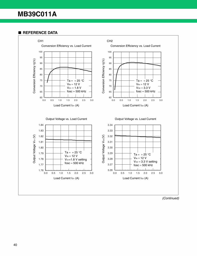
REFERENCE DATA
(Continued)
CH1 CH2
Conversion Efficiency vs. Load Current Conversion Efficiency vs. Load Current
Con
vers
ion
Effi
cien
cyη(
%)
Con
vers
ion
Effi
cien
cyη(
%)
Load Current IO1 (A) Load Current IO2 (A)
Output Voltage vs. Load Current Output Voltage vs. Load Current
Out
put V
olta
geV
O1
(V)
Out
put V
olta
geV
O2 (V
)
Load Current IO1 (A) Load Current IO2 (A)
100
95
90
85
80
75
70
65
600.0 0.5 1.0 1.5 2.0 2.5 3.0
Ta = + 25 °CVIN = 12 VVO1 = 1.8 Vfosc = 500 kHz
0.0 0.5 1.0 1.5 2.0 2.5 3.0
100
95
90
85
80
75
70
65
60
Ta = + 25 °CVIN = 12 VVO2 = 3.3 Vfosc = 500 kHz
1.84
1.83
1.82
1.81
1.80
1.79
1.78
1.77
1.760.0 0.5 1.0 1.5 2.0 2.5 3.0
Ta = + 25 °CVIN = 12 VVO1=1.8 V settingfosc = 500 kHz
3.34
3.33
3.32
3.31
3.30
3.29
3.28
3.27
3.260.0 0.5 1.0 1.5 2.0 2.5 3.0
Ta = + 25 °CVIN = 12 VVO2 = 3.3 V settingfosc = 500 kHz
MB39C011A
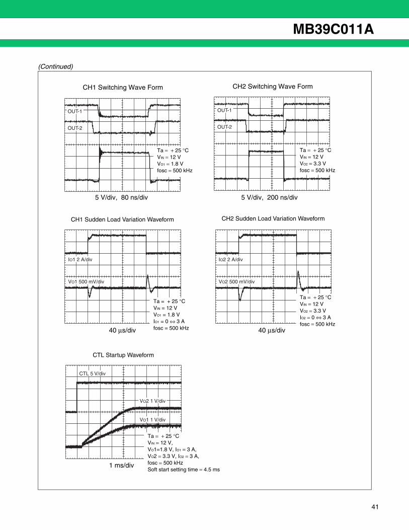
(Continued)
OUT-1
OUT-2
Ta = + 25 °CVIN = 12 VVO1 = 1.8 Vfosc = 500 kHz
OUT-1
OUT-2
Ta = + 25 °CVIN = 12 VVO2 = 3.3 Vfosc = 500 kHz
IO1 2 A/div
VO1 500 mV/div
IO2 2 A/div
VO2 500 mV/div
CTL 5 V/div
VO2 1 V/div
VO1 1 V/div
CH1 Switching Wave Form CH2 Switching Wave Form
5 V/div, 80 ns/div 5 V/div, 200 ns/div
CH1 Sudden Load Variation Waveform CH2 Sudden Load Variation Waveform
40 µs/div 40 µs/div
CTL Startup Waveform
1 ms/div
Ta = + 25 °CVIN = 12 V,VO1=1.8 V, IO1 = 3 A, VO2 = 3.3 V, IO2 = 3 A, fosc = 500 kHzSoft start setting time = 4.5 ms
Ta = + 25 °CVIN = 12 VVO1 = 1.8 VIO1 = 0 ⇔ 3 Afosc = 500 kHz
Ta = + 25 °CVIN = 12 VVO2 = 3.3 VIO2 = 0 ⇔ 3 Afosc = 500 kHz
41

MB39C011A
42
USAGE PRECAUTION1. Do not configure the IC over the maximum ratings.
If the IC is used over the maximum ratings, the LSI may be permanently damaged.It is preferable for the device to normally operate within the recommended usage conditions. Usage outside ofthese conditions can have a bad effect on the reliability of the LSI.
2. Use the device within the recommended operating conditions.
The recommended operating conditions are under which the LSI is guaranteed to operate. The electrical ratings are guaranteed when the device is used within the recommended operating conditionsand under the conditions stated for each item.
3. Printed circuit board ground lines should be set up with consideration for common imped-ance.
4. Take appropriate measures against static electricity.• Containers for semiconductor materials should have anti-static protection or be made of conductive material.• After mounting, printed circuit boards should be stored and shipped in conductive bags or containers.• Work platforms, tools, and instruments should be properly grounded.• Working personnel should be grounded with resistance of 250 kΩ to 1 MΩ between body and ground.
5. Do not apply negative voltages.
The use of negative voltages below − 0.3 V may create parasitic transistors on LSI lines, which can causemalfunctions.
ORDERING INFORMATION
EV BOARD ORDERING INFORMATION
RoHS COMPLIANCE INFORMATION OF LEAD (Pb) FREE VERSION
The LSI products of Fujitsu Microelectronics with “E1” are compliant with RoHS Directive, and has observed thestandard of lead, cadmium, mercury, Hexavalent chromium, polybrominated biphenyls (PBB), and polybromi-nated diphenyl ethers (PBDE). Products that are complied with this standard have “E1” appended to the partnumber.
Part number Package Remarks
MB39C011APFT-E116-pin plastic TSSOP
(FPT-16P-M07)Lead Free version
Part number EV board version No. Remarks
MB39C011AEVB-01 Board rev.1.0 TSSOP-16-pin
MB39C011A
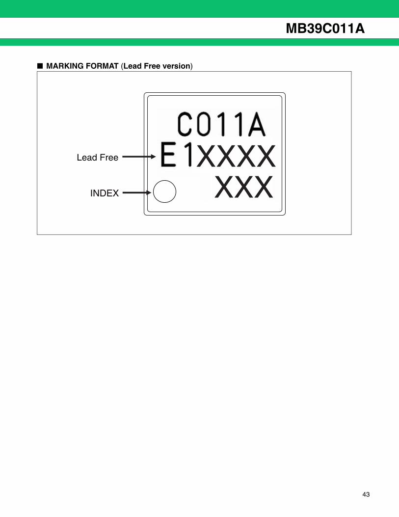
MARKING FORMAT (Lead Free version)
XXXXXXXINDEX
Lead Free
43
MB39C011A
44
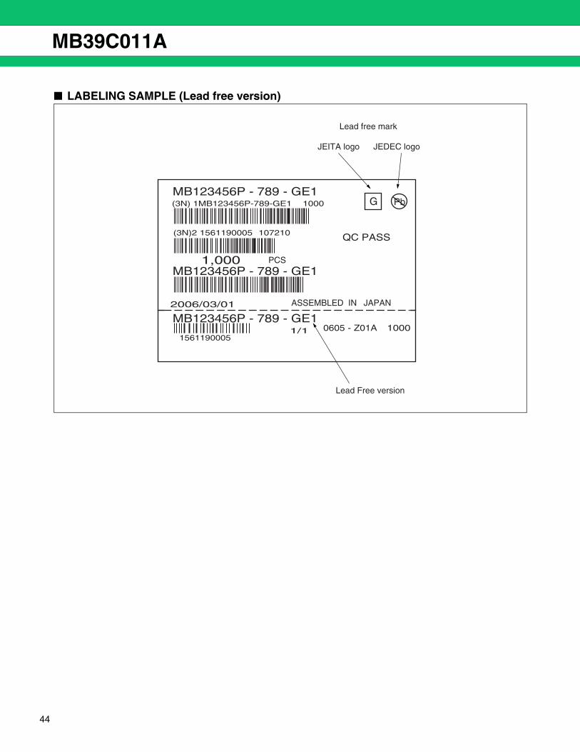
LABELING SAMPLE (Lead free version)
2006/03/01 ASSEMBLED IN JAPAN
G
QC PASS
(3N) 1MB123456P-789-GE1 1000
(3N)2 1561190005 107210
1,000 PCS
0605 - Z01A 10001/11561190005
MB123456P - 789 - GE1
MB123456P - 789 - GE1
MB123456P - 789 - GE1
Pb
Lead Free version
Lead free mark
JEITA logo JEDEC logo

MB39C011A
MB39C011APFT-E1 RECOMMENDED MOUNTING CONDITIONS[Fujitsu Microelectronics Recommended Mounting Conditions]
[Parameters for Each Mounting Method]
(1) IR (infrared reflow)
(2) Manual soldering (partial heating method)
Conditions : Temperature 400 °C Max
Times : 5 s max/pin
Item Condition
Mounting Method IR (infrared reflow), Manual soldering (partial heating method)
Mounting times 2 times
Storage period
Before opening Please use it within two years after
Manufacture.
From opening to the 2ndreflow
Less than 8 days
When the storage period afteropening was exceeded
Please processes within 8 daysafter baking (125 °C, 24H)
Storage conditions 5 °C to 30 °C, 70%RH or less (the lowest possible humidity)
260 °C
(e)
(d')
(d)
255 °C
170 °C
190 °C
RT (b)
(a)
(c)
to
Note : Temperature : the top of the package body
(a) Temperature Increase gradient : Average 1 °C/s to 4 °C/s (b) Preliminary heating : Temperature 170 °C to 190 °C, 60s to 180s (c) Temperature Increase gradient : Average 1 °C/s to 4 °C/s (d) Actual heating : Temperature 260 °C Max; 255 °C or more, 10s or less (d’) : Temperature 230 °C or more, 40s or less
orTemperature 225 °C or more, 60s or less
orTemperature 220 °C or more, 80s or less
(e) Cooling : Natural cooling or forced cooling
H rank : 260 °C Max
45

MB39C011A
46
PACKAGE DIMENSIONS
Please confirm the latest Package dimension by following URL.http://edevice.fujitsu.com/package/en-search/
16-pin plastic TSSOP Lead pitch 0.65 mm
Package width ×package length
4.40 × 5.00 mm
Lead shape Gullwing
Sealing method Plastic mold
Mounting height 1.10mm MAX
Weight 0.06g
Code(Reference)
P-TSSOP16-4.4×5.0-0.65
16-pin plastic TSSOP(FPT-16P-M07)
(FPT-16P-M07)
C 2003 FUJITSU LIMITED F16020S-c-3-3
5.00±0.10(.197±.004)
4.40±0.10 6.40±0.20(.252±.008)(.173±.004)
0.10(.004)
0.65(.026) 0.24±0.08(.009±.003)
1 8
16 9
"A"
0.17±0.05(.007±.002)
M0.13(.005)
Details of "A" part
0~8˚
(.024±.006)0.60±0.15
(0.50(.020))
0.25(.010)
(.041±.002)1.05±0.05
(Mounting height)
0.07+0.03–0.07
+.001–.003.003
(Stand off)
LEAD No.
INDEX
*1
*2
Dimensions in mm (inches).Note: The values in parentheses are reference values.
Note 1) *1 : Resin protrusion. (Each side : +0.15 (.006) Max).Note 2) *2 : These dimensions do not include resin protrusion.Note 3) Pins width and pins thickness include plating thickness.Note 4) Pins width do not include tie bar cutting remainder.
MB39C011A
MEMO
47
FUJITSU MICROELECTRONICS LIMITEDShinjuku Dai-Ichi Seimei Bldg. 7-1, Nishishinjuku 2-chome, Shinjuku-ku,Tokyo 163-0722, Japan Tel: +81-3-5322-3347 Fax: +81-3-5322-3387http://jp.fujitsu.com/fml/en/
For further information please contact:
North and South AmericaFUJITSU MICROELECTRONICS AMERICA, INC.1250 E. Arques Avenue, M/S 333Sunnyvale, CA 94085-5401, U.S.A.Tel: +1-408-737-5600 Fax: +1-408-737-5999http://www.fma.fujitsu.com/
EuropeFUJITSU MICROELECTRONICS EUROPE GmbHPittlerstrasse 47, 63225 Langen,GermanyTel: +49-6103-690-0 Fax: +49-6103-690-122http://emea.fujitsu.com/microelectronics/
KoreaFUJITSU MICROELECTRONICS KOREA LTD.206 KOSMO TOWER, 1002 Daechi-Dong,Kangnam-Gu,Seoul 135-280KoreaTel: +82-2-3484-7100 Fax: +82-2-3484-7111http://www.fmk.fujitsu.com/
Asia PacificFUJITSU MICROELECTRONICS ASIA PTE LTD.151 Lorong Chuan, #05-08 New Tech Park,Singapore 556741Tel: +65-6281-0770 Fax: +65-6281-0220http://www.fujitsu.com/sg/services/micro/semiconductor/
FUJITSU MICROELECTRONICS SHANGHAI CO., LTD.Rm.3102, Bund Center, No.222 Yan An Road(E),Shanghai 200002, ChinaTel: +86-21-6335-1560 Fax: +86-21-6335-1605http://cn.fujitsu.com/fmc/
FUJITSU MICROELECTRONICS PACIFIC ASIA LTD.10/F., World Commerce Centre, 11 Canton RoadTsimshatsui, KowloonHong KongTel: +852-2377-0226 Fax: +852-2376-3269http://cn.fujitsu.com/fmc/tw
All Rights Reserved.
The contents of this document are subject to change without notice. Customers are advised to consult with sales representatives before ordering.The information, such as descriptions of function and application circuit examples, in this document are presented solely for the purposeof reference to show examples of operations and uses of FUJITSU MICROELECTRONICS device; FUJITSU MICROELECTRONICSdoes not warrant proper operation of the device with respect to use based on such information. When you develop equipment incorporat-ing the device based on such information, you must assume any responsibility arising out of such use of the information. FUJITSU MICROELECTRONICS assumes no liability for any damages whatsoever arising out of the use of the information.Any information in this document, including descriptions of function and schematic diagrams, shall not be construed as license of the useor exercise of any intellectual property right, such as patent right or copyright, or any other right of FUJITSU MICROELECTRONICSor any third party or does FUJITSU MICROELECTRONICS warrant non-infringement of any third-party's intellectual property right orother right by using such information. FUJITSU MICROELECTRONICS assumes no liability for any infringement of the intellectualproperty rights or other rights of third parties which would result from the use of information contained herein.The products described in this document are designed, developed and manufactured as contemplated for general use, including withoutlimitation, ordinary industrial use, general office use, personal use, and household use, but are not designed, developed and manufacturedas contemplated (1) for use accompanying fatal risks or dangers that, unless extremely high safety is secured, could have a serious effectto the public, and could lead directly to death, personal injury, severe physical damage or other loss (i.e., nuclear reaction control in nuclear facility, aircraft flight control, air traffic control, mass transport control, medical life support system, missile launch control inweapon system), or (2) for use requiring extremely high reliability (i.e., submersible repeater and artificial satellite).Please note that FUJITSU MICROELECTRONICS will not be liable against you and/or any third party for any claims or damages arisingin connection with above-mentioned uses of the products.Any semiconductor devices have an inherent chance of failure. You must protect against injury, damage or loss from such failures byincorporating safety design measures into your facility and equipment such as redundancy, fire protection, and prevention of over-currentlevels and other abnormal operating conditions.Exportation/release of any products described in this document may require necessary procedures in accordance with the regulations ofthe Foreign Exchange and Foreign Trade Control Law of Japan and/or US export control laws.The company names and brand names herein are the trademarks or registered trademarks of their respective owners.
Edited Strategic Business Development Dept.