Embed Size (px)
Citation preview

Exhibitor Seminars - December 3rd, 20081
Seminars by ExhibitorsDecember 3rd, 2008
ASSEMBLY STRATEGIES FOR 3D-IC INTEGRATIONWAFER-TO-WAFER VERSUS CHIP-TO-WAFER
Gilbert LecarpentierProduct Manager
Abstract:With the advent of 3D Integration concepts as a potential enabler for the continuation of Moore’s law, the aligned wafer bonding requirements have shifted significantly.Chip-to-Wafer bonding and wafer reconstruction represent alternative or complementary solutions to improve yield and chip size flexibility; pros and cons of the two methods are reviewed.

Exhibitor Seminars - December 3rd, 20082
SET AT A GLANCE
Founded in 1975SUSS MicroTec Device Division from 1993 to 200707/2007: SET (MBO)01/2008: Subsidiary of ReplisaurusLocated in the French Alps (Grenoble: 90’ – Geneva: 30’)58 employees
Acceptance - Class 100 (30 m²)Assembly - Class 10,000 (546 m²) Test Area - Class 1,000 (149 m²)

Exhibitor Seminars - December 3rd, 20083
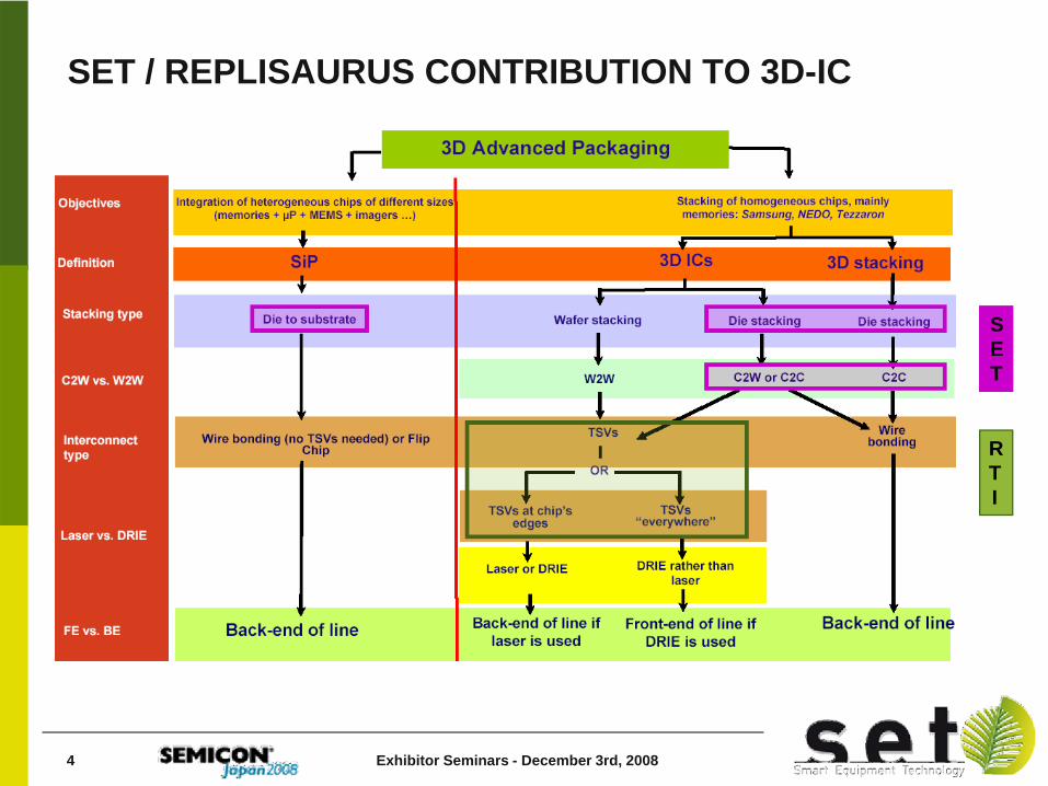
SET / REPLISAURUS CONTRIBUTION TO 3D-IC
SET
RTI
Exhibitor Seminars - December 3rd, 20084
SET / REPLISAURUS CONTRIBUTION TO 3D-IC
SET
RTI

Exhibitor Seminars - December 3rd, 20085
AGENDA
IntroductionWafer Stacking Vs Chip-to-Wafer BondingWafer to Wafer Bonding
Wafer Bonding Techniques
Align and Bond Process
Chip to Wafer / Chip to Chip BondingDie Bonding Techniques
Assembly scenarios
Examples
Summary
1st transistor, 1947

Exhibitor Seminars - December 3rd, 20086
INTRODUCTION
3D Assembly by Chip or Wafer Stacking enables the development of Very High Density, Multifunction Devices and satisfies the demand for Higher Packaging Miniaturization
3D-Assemby TechnologiesChip-to-ChipChip-to-WaferWafer-to-Wafer (Wafer Stacking)
Source
3D - WB 3D - TSV
2D

Exhibitor Seminars - December 3rd, 20087
WAFER TO WAFER Vs. CHIP-TO-WAFER
Device Bonder
Wafer Stacking technique Chip-to-Wafer technique
Wafer Bonder

Exhibitor Seminars - December 3rd, 20088
W2W Vs. C2W APPLICATIONS
Wafer To WaferMemory: DRAM, PCRAM, FERAM, MRAMFPGASensorsProcessors1,000 to 1,000,000 connections per square millimeters
Chip-to-WaferMemory to LogicMixed Materials (GaAs, InP)Known good die yield ++1,000 to 1,000,000 connections per square millimeters
Source: Terrazon Semiconductors
Source

Exhibitor Seminars - December 3rd, 20089
CHIP TO WAFER Vs. WAFER STACKING
WAFER STACKING☺ High Throughput
Wafer LevelComponent size must be identicalYield ?
CHIP-TO-WAFERLow Throughput
Single Chip Placement☺ High Yield
Known Good Die☺ Flexibility
Component sizeDifferent Technologies

Exhibitor Seminars - December 3rd, 200810
WAFER STACKING Vs. CHIP-TO-WAFER
Device Bonder
Wafer Stacking technique Chip-to-Wafer technique
Wafer Bonder

Exhibitor Seminars - December 3rd, 200811
WAFER BONDING TECHNIQUES
WBT Withoutintermediate layer
WBT Withintermediate layer
Si directbonding
Solderbonding
Glass fritbonding
Adhesivebonding
Anodic bonding
TC metalbonding
Eutecticbonding
Exhibitor Seminars - December 3rd, 200812
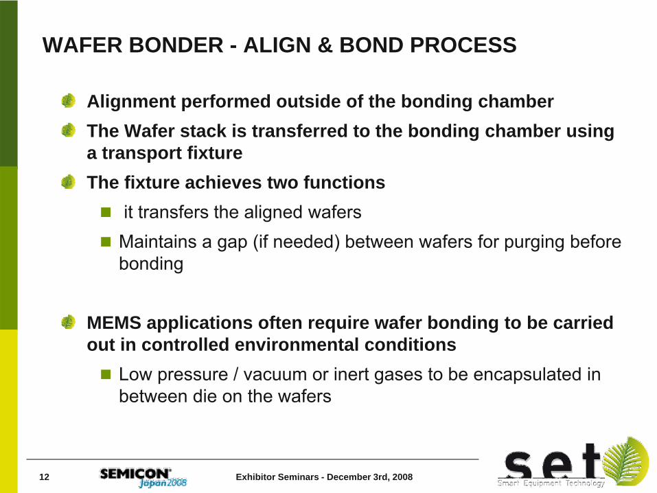
WAFER BONDER - ALIGN & BOND PROCESS
Alignment performed outside of the bonding chamberThe Wafer stack is transferred to the bonding chamber using a transport fixtureThe fixture achieves two functions
it transfers the aligned wafersMaintains a gap (if needed) between wafers for purging before bonding
MEMS applications often require wafer bonding to be carried out in controlled environmental conditions
Low pressure / vacuum or inert gases to be encapsulated in between die on the wafers

Exhibitor Seminars - December 3rd, 200813
WAFER BONDER - ALIGN & BOND PROCESS
Wafer clamp into fixture
after alignment
Bond
Load wafersinto
Bond Aligner
Full autoBond cluster
Semi-auto

Exhibitor Seminars - December 3rd, 200814
WAFER BONDER: TYPICAL BONDING SEQUENCE
Load fixture with alignedwafers into the bond chamber
Bond wafers by applyingforce, heat, electrical current and/or pressurized confinement

Exhibitor Seminars - December 3rd, 200815
WAFER STACKING Vs. CHIP-TO-WAFER
Device Bonder
Wafer Stacking technique Chip-to-Wafer technique
Wafer Bonder

Exhibitor Seminars - December 3rd, 200816
CHIP BONDING PROCESSES (FC)
Device Bonder Pick and Place
ICANCA ACA
Bumps Au, Ni/Au with Adhesive
Reflow
TemperatureFluxing
BumpsAu, In, …
PbSn, SnAg, 80AuSn, In Bumps
PbSn, SnAg, InBumps (+ flux)
TemperatureGap control
Thermo compression
Temperature, ForceGap control
No intermediate layer
Direct
LowForce

Exhibitor Seminars - December 3rd, 200817
CHIP TO WAFER – FACE UP CHIP PLACEMENT
Chip are placed one after each other
They can be aligned individually with respect to wafer/substrate pattern
Alternatively, they can be aligned prior to pick up and placed using a step and repeat approach if the wafer/substrate is blank
The accuracy is then the accuracy of the Wafer/Substrate X/Y stage
The operation can be repeated to place another chip on top of the first one >> 3D-Stacking

Exhibitor Seminars - December 3rd, 200818
CHIP TO WAFER – FACE UPCHIP PLACEMENT & BONDING
Chip are placed one after each other
They can be aligned individually with respect to wafer/substrate pattern
Alternatively, they can be aligned prior to pick up and placed using a step and repeat approach if the wafer/substrate is blank
The accuracy is then the accuracy of the Wafer/Substrate X/Y stage
The operation can be repeated to place another chip on top of the first one >> 3D-Stacking
Chip-to-Substrate and/or Chip-to-Chip connections are then made with wire bonding

Exhibitor Seminars - December 3rd, 200819
CHIP TO WAFER – FLIP CHIP PLACEMENT (AND BONDING)
The Placement Sequence is similar to the Sequence used for Face UP Placement
The Connections are visible on the Wafer and can be used to perform Chip-to-Wafer Alignment
Electrical connections is performed simultaneously to chip bonding
The operation can be repeated several times to place another chip on top of the first one
Electrical connections is performed simultaneously to chip bonding
It is possible to mix Face Up & Flip Chip

Exhibitor Seminars - December 3rd, 200820
CHIP-TO-WAFER -- FACE UP Vs FLIP CHIP
FACE UP
☺ Rework ability, Testability
Wire Bond Serial process
Wire Bond Long connection
FLIP CHIP
Rework (only possible for Reflow)
☺ Global bonding
☺ Bumps = Short connection

Exhibitor Seminars - December 3rd, 200821
CHIP-TO-WAFER AND WAFER-TO-WAFERCOMPLEMENTARY TECHNIQUES
To enable Wafer-to-Wafer bonding with Chips of different size, it is possible to rebuild a Wafer by placing Chips accurately on a given mesh with a accurate device bonder
The gap between chips is then filled with appropriated resin
If Flip Chip Technique is used, it guarantees that the top surface of all chips is on a plan and enables thinning of the reconstructed wafer

Exhibitor Seminars - December 3rd, 200822
CHIP-TO-WAFER AND WAFER-TO-WAFERCOMPLEMENTARY TECHNIQUES
Photo-resist coating, baking
At this stage, it is possible to process the components at wafer level using standard photolithography process
Masking, Development, etchingetc.

Exhibitor Seminars - December 3rd, 200823
EXAMPLE OF APPLICATIONS
MEMS RF Device assembled to a logic system with Package on Package Approach
Memory stack: 2D Flip Chip Bonding on Silicon Substrates stacked together
Memory stack using Trough Silicon Vias
Courtesy: IMEC
Source: Samsung

Exhibitor Seminars - December 3rd, 200824
EXAMPLE OF APPLICATION
Chip-to-Wafer ProcessChips Placement (Flip Chip)
Wafer Level ProcessingPottingPad’s RedistributionThinning and Dicing
Chip-to-Chip ProcessStacking3D interconnect

Exhibitor Seminars - December 3rd, 200825
EXAMPLE OF APPLICATIONENCAPSULATION ON WAFER
Placement and Sealing On the entire matrixWafer with
« Caps or Window »Wafer with
« Chips to Encapsulate »
Encapsulation Chip to Wafer C2W
Encapsulation Wafer to Wafer W2W
Wafer with« Caps or Functionalized Window »
Wafer with« Chips to Encapsulate »

Exhibitor Seminars - December 3rd, 200826
SEALING AND FINAL ALIGNMENTBY COLLECTIVE REFLOW
PICK/PLACEHigh Speed Placement of Functionalized CapsAlignment requirementApplication dependent
5 ~ 10 µm
BONDINGSelf Alignment Fast Temperature RampHermetic Encapsulation under Controlled Atmosphere
Pick & Place =Alignment and Deposition
Bonding = T >Tf
Controlled Atmosphere
Cadence +

Exhibitor Seminars - December 3rd, 200827
SIMULTANEOUS HERMETIC SEALING AND CONNECTION -- PROCESS FLOW
Cap is tacked to the substrateHigher Connection Bumps maintain a Gap ensuring Gas Flow and Pumping between Inner Solder Cap Ring and MEMS WaferWetting Pads Geometry Controls Cap Collapsing during ReflowSealing Ring contacts the Wetting Ring on the opposite wafer, capturing the required atmosphere inside the MEMS cavity.
Controlled atmosphereor vacuum
Solder ring
interconnection
MEMS
Controlled Collapse Hermetic Sealing
Oxide reductionVacuumGettering
Cap
MEMS wafer

Exhibitor Seminars - December 3rd, 200828
COLLECTIVE REFLOW IN THE EMBEDDEDCHAMBER FOR VACUUM OR GAS CONFINEMENT
Having the Chamber included inside the Placement Tool
eliminates the risk of Chips shifting during wafer transport

Exhibitor Seminars - December 3rd, 200829
DEMONSTRATOR -- SEALING RESULTS
Measured ring and bump height for 4 different bump & ring designs1,2,3,4 using a « sixteen bumps / one ring design »
SEALED COMPONENT
Bottom chip
Indium bumpIndium Ring
Gold platedUBM lands
FLIP-CAP
Cap chip
Before soldering After soldering (separate)Bump height Ring height Bump height Ring height
1 39,7 18,1 10,9 11,52 32,4 15,6 10 10,73 52 22,2 10,5 14,44 44,6 19,3 10 13,3
Bump only
Ring only
FINAL = Bumps + Ring

Exhibitor Seminars - December 3rd, 200830
SUMMARY (1/2)
Various pieces of equipment are available to suit different degrees of
automation or flexibility
Device Bonder can be used in combination with Wafer Bonder to
increase throughput:
In Thermo-compression mode;Chips are Tacked and Final Bond
occurs in the Wafer Bonder
When Using Reflow Bonding, a Chamber can be used to Reflow
under Vacuum or Gas environment

Exhibitor Seminars - December 3rd, 200831
SUMMARY (2/2)3D Assembly + Multifunction devices
+ Packaging density increasesWafer-to-Wafer + Higher Throughput (globalization)
- Overlay control(slightly better with In Situ Aligner bonder)
- Component sizes- Yield
Chip-to-Wafer + Yield (Known Good Die – KGD)+ Flexibility- Lower Throughput (serialization)
Higher throughput can be achieved by 2-Step approach, placement then collective bonding
● Thermo Compression, using a wafer Bonder● Collective Reflow Chamber as illustrated in the previous example
W2W, C2W and C2C are complementary techniques

Exhibitor Seminars - December 3rd, 200832
Seminars by ExhibitorsDecember 3rd, 2008
ASSEMBLY STRATEGIES FOR 3D-IC INTEGRATIONWAFER-TO-WAFER VERSUS CHIP-TO-WAFER
Gilbert LecarpentierProduct Manager
Abstract:With the advent of 3D Integration concepts as a potential enabler for the continuation of Moore’s law, the aligned wafer bonding requirements have shifted significantly.Chip-to-Wafer bonding and wafer reconstruction represent alternative or complementary solutions to improve yield and chip size flexibility; pros and cons of the two methods are reviewed.
Thank you for your attention >> Questions?