Embed Size (px)
Citation preview

Elecraft Transverter Models XV50, XV144, XV222 Assembly Manual
Rev E, January 31, 2012
Copyright © 2012, Elecraft; All Rights Reserved


Table of Contents
INTRODUCTION ......................................................................................................................................................................... 1 CUSTOMER SERVICE AND SUPPORT .................................................................................................................................... 1
Technical Assistance ........................................................................................................................................................................................................... 1
Repair / Alignment Service (We want to make sure everyone succeeds!) .......................................................................................................................... 1
PREPARING FOR ASSEMBLY .................................................................................................................................................. 2 Overview of the Kit ............................................................................................................................................................................................................... 2
Tools Required ..................................................................................................................................................................................................................... 2
Preventing Electrostatic Discharge Damage ....................................................................................................................................................................... 3
Unpacking and Inventory ..................................................................................................................................................................................................... 3
Identifying Parts ................................................................................................................................................................................................................... 3
Assembly Process ................................................................................................................................................................................................................ 5
Forming Component Leads .................................................................................................................................................................................................. 5
Step-By-Step Procedures .................................................................................................................................................................................................... 5
Soldering, Desoldering and Plated-Through Holes ............................................................................................................................................................. 6
PARTS INVENTORY .................................................................................................................................................................. 7 FRONT PANEL PCB ASSEMBLY ............................................................................................................................................ 21
Uninstalled Components .................................................................................................................................................................................................... 25
RF PCB ASSEMBLY – PART I ................................................................................................................................................. 26 RF PCB ASSEMBLY – PART II ................................................................................................................................................ 39
XV50 – 50 MHz Transverter............................................................................................................................................................................................... 39
XV144 –144 MHz Transverter ........................................................................................................................................................................................... 41
XV222 – 222 MHz Transverter .......................................................................................................................................................................................... 44
RF PCB ASSEMBLY – PART III ............................................................................................................................................... 47 FINAL ASSEMBLY ................................................................................................................................................................... 50 FINAL TEST AND ALIGNMENT ............................................................................................................................................... 54

- 1 -
Introduction This is the assembly manual for the Elecraft XV50, XV144 or XV222 transverter kits. A separate manual covers the assembly of the Elecraft XV432 transverter.
Full details of the Elecraft transverters including specifications, installation, operation, circuit descriptions, options and modifications available, troubleshooting and maintenance instructions are included in the Owner’s Manual which accompanies this kit.
This is an intermediate to advanced kit, yet you'll be surprised at how uncomplicated it is to build. All of the radio frequency (RF) circuits are on one printed circuit board (PCB). A second smaller PCB holds the microcontroller and front-panel LEDs. High-quality, double-sided PCBs are used, with plated-through holes for optimal RF performance. Point-to-point wiring is minimal. All components to be installed have wire leads; the few surface-mount devices required are pre-installed on the PCB.
This kit uses just one toroidal inductor, which is easy to wind. However, if you prefer not to wind this inductor yourself, you can order one pre-wound with the leads tinned and ready to install from an Elecraft-qualified source. Ordering information is on our web site at www.elecraft.com.
Customer Service and Support Technical Assistance You can send e-mail to [email protected] and we will respond quickly - typically the same day Monday through Friday. Telephone assistance is available from 9 A.M. to 5 P.M. Pacific time (weekdays only) at 831-763-4211. Please use e-mail rather than calling when possible since this gives us a written record of the details of your problem and allows us to handle a larger number of requests each day. Repair / Alignment Service (We want to make sure everyone succeeds!) If necessary, you may return your Elecraft product to us for repair or alignment. (Note: We offer unlimited email and phone support to get your kit running, so please try that route first as we can usually help you find the problem quickly.)
Important: You must contact Elecraft before mailing your product to obtain authorization for the return, what address to ship it to and current information on repair fees and turnaround times. (Frequently we can determine the cause of your problem and save you the trouble of shipping it back to us.) Our repair location is different from our factory location in Aptos. We will give you the address to ship your kit to at the time of repair authorization. Packages shipped to Aptos without authorization will incur an additional shipping charge for reshipment from Aptos to our repair depot.
Elecraft's 1-Year Limited Warranty This warranty is effective as of the date of first consumer purchase (or if shipped from factory, date product is shipped to customer). It covers both our kits and fully assembled products. For kits, before requesting warranty service, you should fully complete the assembly, carefully following all instructions in the manual. Who is covered: This warranty covers the original owner of the Elecraft product as disclosed to Elecraft at the time of order. Elecraft products transferred by the purchaser to a third party, either by sale, gift or other method, who is not disclosed to Elecraft at the time of original order, are not covered by this warranty. If the Elecraft product is being bought indirectly for a third party, the third party's name and address must be provided to Elecraft at time of order to insure warranty coverage. What is covered: During the first year after date of purchase, Elecraft will replace defective or missing parts free of charge (post-paid). We will also correct any malfunction to kits or assembled units caused by defective parts and materials. Purchaser pays inbound shipping to Elecraft for warranty repair, Elecraft will pay shipping to return the repaired equipment to you by UPS ground service or equivalent to the continental USA and Canada. Alaska, Hawaii and outside U.S. and Canada actual return shipping cost paid by owner. What is not covered: This warranty does not cover correction of kit assembly errors. It also does not cover misalignment; repair of damage caused by misuse, negligence, or builder modifications; or any performance malfunctions involving non-Elecraft accessory equipment. The use of acid-core solder, water-soluble flux solder, or any corrosive or conductive flux or solvent will void this warranty in its entirety. Also not covered is reimbursement for loss of use, inconvenience, customer assembly or alignment time, or cost of unauthorized service. Limitation of incidental or consequential damages: This warranty does not extend to non-Elecraft equipment or components used in conjunction with our products. Any such repair or replacement is the responsibility of the customer. Elecraft will not be liable for any special, indirect, incidental or consequential damages, including but not limited to any loss of business or profits.

- 2 -
Preparing for Assembly
Overview of the Kit The Elecraft XV transverters use modular construction, both physically and electrically. This concept extends to the chassis (Figure 1). Any chassis element can be removed to provide access.
Figure 1. XV Transverter Modular Cabinet Parts.
There are two printed circuit boards (PCBs) in the transverter: the front panel PCB, which sits vertically behind the front panel, and the large RF PCB visible in the cover photograph.
The PCBs are interconnected using board-to-board connectors which eliminates the need for a wiring harness. Gold-plated contacts are used on these connectors for reliability.
Tools Required You will need the following tools to build this kit1:
Fine-tip temperature-controlled soldering station with 700 or 800F tip (370-430C). Do not use a high-wattage iron or gun since this can damage pads, traces, or the parts themselves.
IC grade, small-diameter (.031”) solder (Kester #44 or equivalent). Desoldering tools and supplies are invaluable if you make any
modifications or need to do any repairs. Narrow solder wick or a good vacuum desoldering tool such as the Soldapullt® model DS017LS are recommended. See Soldering, Desoldering and Plated-Through Holes, on page 6 for more information.
i DO NOT use acid-core solder, water-soluble flux solder, additional flux or solvents of any kind. Use of any of these will void your warranty.
Screwdrivers: a small, #2 Phillips and a small flat-blade for slotted screws.
Needle-nose pliers. Small-point diagonal cutters, preferably flush-cutting. Digital Multimeter (DMM) for voltage checks and confirming
resistor values. A DMM with capacitance measurement capability is desirable, but not required.
Noise generator (Elecraft N-Gen or equivalent) or signal generator with output in the RF frequency range of the transverter.
RF power meter capable of measuring RF power levels up to 25 watts at the frequency used by the transverter.
50-ohm dummy load capable of handling 25 watts, minimum.
1 Refer to www.elecraft.com for tool sources and solder recommendations.
BACK PANEL
LEFT SIDE PANEL
TOPCOVER
FRONT PANEL
BOTTOMCOVER
(RIGHT SIDEPANEL NOTSHOWN)

- 3 -
Preventing Electrostatic Discharge Damage
Your XV transverter uses integrated circuits and transistors that can be damaged by electrostatic discharge (ESD). Problems caused by ESD can be difficult to troubleshoot because components may be degraded but still operating, rather than fail completely.
To avoid such problems, touch an unpainted, grounded metal surface before handling any such components and occasionally as you build, especially after moving about.
For maximum protection, we recommend you take the following antistatic precautions (listed in order of importance):
1. Leave ESD-sensitive parts in their antistatic packaging until you install them. The packaging may be a special bag, other container or the leads may be inserted in conductive foam (Figure 2). Parts which are especially ESD-sensitive are identified in the parts list.
2. Wear a conductive wrist strap with a series 1 megohm resistor. DO NOT ground yourself directly as this poses a serious shock hazard.
3. Make sure your soldering iron has a grounded tip.
4. Use an antistatic mat on your work bench.
Figure 2. A common antistatic packaging is conductive foam which
keeps all of the terminals of a device at the same potential.
Unpacking and Inventory We strongly recommend that you do an inventory of the parts before beginning to assemble the kit. Even if you don’t count all the parts, an inventory is helpful to familiarize yourself with them. A complete parts list is included in the next section.
Identifying Parts The parts list contains illustrations of the parts to help you identify them. Identifying marks on the individual parts are shown in the text in parenthesis. For example, “Transistor Q4 (PN2222)…” indicates a transistor, Q4, which may be located in the parts list that has the characters shown in parenthesis printed on it. Sometimes these letters are not obvious. For example, they may be printed in light gray on a black body. Also, there may be other marks on the device in addition to the letters listed.
Identifying Resistors
Resistors are identified by their power capacity and their resistance value. The power rating in watts determines the physical size of a resistor. The most common resistors are 1/4 watt. Higher wattage resistors are proportionately larger. The resistance value and wattage of each resistor is shown in the Parts Lists and in the individual steps of the assembly procedures. The silk-screened outlines on the PCBs indicate the relative physical size of the resistors as well.
Most resistors use a color code. The color bands are listed in the text along with the values of each resistor. For example, “R4, 100k (brn-blk-yel)…” indicates a 100k ohm resistor and the colors to look for are brown, black and yellow, starting with the band nearest the end of the resistor.
Some resistors use numbers instead of color bands. For example, an 820 ohm resistor might be stamped with the digits 821 instead of having gray, red and brown color bands. Some larger resistors have their value in ohms stamped on the body using numbers. For, example the 820 ohm resistor would be stamped with 820 instead of 821 as described above. Normally, when the value is shown in ohms it will be followed with the word “ohms” or the Greek letter omega: Ω

- 4 -
Reading Resistor Color Codes
It is very helpful if you learn to read the color codes. A color-code chart showing how to read the four-color bands on resistors with a 5% or 10% tolerance is shown in Figure 3. 1% resistors are similar except that they use a fifth band to provide a way of showing another significant digit. For example, a 1,500 ohm (1.5 k-ohm) 5% resistor has the color bands brown, green and red signifying one, five and two zeros. A 1,500 ohm (1.5 k-ohm) 1% tolerance resistor has the color bands brown, green, black and brown signifying one, five, zero, and one zero.
The optional band shown in Figure 3 indicates other performance specifications for the resistor. When used, it is separated from the other color bands by a wider space.
i If in doubt of a resistor’s value, use a DMM. It may be difficult to see the colors on some resistors, particularly 1% tolerance resistors with a dark blue body. Do not be concerned with minor deviations of your DMM reading from the expected value. Typical errors in most DMMs and the tolerances of the resistors normally produce readings that are slightly different from the value indicated by the color bands.
Identifying Molded Inductors
Small molded inductors have color bands that use the same numeric values as resistors but they start near the center of the inductor and work toward the end. These colors are listed in the text after the value of the inductor, for example: 27H (red-vio-blk). The red stripe would be near the center of the inductor and the black stripe would be closer to the end. On very small chokes, the first color will be only slightly farther from one end than the last color. There may be a variety of other stripes on inductors as well, indicating their tolerance, conformance to certain specifications and other data.
FIRST DIGIT TOLERANCE:OPTIONAL
SECOND DIGITMULTIPLIER
BlackBrownRedOrangeYellowGreenBlueVioletGrayWhiteSilverGold
0123456789--
X 1X 10X 100X 10KX 10KX 100KX 1M---X 0.01X 0.1
COLOR DIGIT MULTIPLIER
GOLD = 5%SILVER = 10%
Figure 3. Resistor Color Code.
Identifying Capacitors
Capacitors are identified by their value and the spacing of their leads.
Small-value fixed capacitors usually are marked with one, two or three digits and no decimal point. The significant digits are shown in parenthesis in the text. For example: “C2, .01 (103)”.
If one or two digits are used, that is always the value in picofarads (pF). If there are three digits, the third digit is the multiplier. For example, a capacitor marked “151” would be 150 pF (15 multiplied by 101). Similarly, “330” is 33 pF and “102” is 1000 pF (or .001 F). You may think of the multiplier value as the number of zeros you need to add on to the end of the value.

- 5 -
Note: In rare cases, a capacitor manufacturer may use “0” as a decimal placeholder. For example, “820” might mean 820 pF rather
than 82 pF. Such exceptions are usually covered in the parts list. If possible, measure the values of all capacitors below .001 F. Most DMMs include capacitance measurement capability.
Fixed capacitors with values of 1000 pF or higher generally use a decimal point in the value, such as .001 or .002. This is the value in microfarads (F). Capacitors also may have a suffix after the value, such as “.001J”.
The lead spacing is noted in the Parts Lists for most capacitors. If two different types of capacitors have the same value, the lead spacing will indicate which one to use. When the lead spacing is important, both the value and the lead spacing is shown in the assembly procedure. For example, “LS 0.1” means that the Lead Spacing is 0.1 in.
Hard-to-Identify Capacitor Values
2.2 pF: These are “disc ceramic” capacitors with round, pillow-shaped bodies about 1/8” (3 mm) in diameter and a black mark on the top. The capacitor should be labeled “2.2” but the marking sometimes requires a magnifying glass to see clearly.
150 pF: These capacitors are marked “151” on one side, but the other side may be marked #21ASD. The “#21” may look like “821”.
Assembly Process There are seven steps in the transverter assembly process:
1. Front panel PCB assembly.
2. RF PCB assembly, part I: Parts common to all models.
3. RF PCB assembly, part II: Band-specific parts.
4. RF PCB assembly, part III: Installing the RF power module.
5. Final assembly.
6. Interconnect cabling.
7. Test and alignment.
Follow the assembly process in the order given. Each part builds on what has been completed before it. For example, the front panel assembly procedure contains details about installing certain parts that are not repeated when similar parts are installed later.
Forming Component Leads Sometimes the space provided for a component on the PCB is larger than the distance between the leads on the part itself. In such cases, you’ll need to carefully bend the leads out and then down to fit the given space. Always use long-nose pliers to accomplish this task, and bend the leads – don’t tug on them. This is especially important with capacitor leads, which are fragile.
Step-By-Step Procedures Perform the assembly steps in each procedure in the order given, and do not skip any steps. Otherwise you may find that you’ve installed one component that hinders the installation of another. When groups of components are installed, they are listed in a logical order as you work around the PCB to reduce the time needed to find where each part goes.
Each step in the assembly procedures has a check box.
Some steps have more than one task. For example, you may be installing a number of components listed. When a step has a number of tasks, each task is indented with space for a check mark:
Check off each task as you complete it.

- 6 -
Soldering, Desoldering and Plated-Through Holes CAUTION: Solder contains lead, and its residue can be toxic. Always wash your hands after handling solder.
The printed circuit boards have circuitry on both sides (“double sided”). PCBs of this type require plated-through holes to complete the electrical connections between the two sides.
When you solder components on these PCBs the solder fills the plated holes making excellent contact. This means that you do not need to leave a large “fillet” or buildup of solder on top of the pads themselves. A small amount of solder will do for all connections.
Unfortunately, removing components from double-sided PCBs can be difficult. To remove a multi-pin component you’ll need to get all of the solder out of every hole to free the leads. You will need to use solder wick or a vacuum desoldering tool (see Techniques below).
The best strategy for avoiding desoldering is to place all components properly the first time. Double-check values, component placement and orientation. Take care to avoid ESD damage to components.
Techniques to Avoid Damaging the PCB when Desoldering
Don’t pull a lead or pin out of a hole unless the solder has been removed completely, or you are applying sufficient heat melt the solder. Otherwise you can pull the entire plating out of the hole.
Limit soldering iron contact to a few seconds at a time.
Use small-size solder wick, about 0.1” (2.5 mm) wide. Use wick on both the top and bottom solder pads when possible. This helps get all of the solder out of the hole.
Buy and learn to use a large hand-operated vacuum desoldering tool such as the Soldapullt® model DS017LS. Small solder suckers are not effective.
When removing ICs and connectors, clip all of the pins at the body first, then remove each pin one at a time, working slowly. You may damage pads and traces by trying to remove a component intact, possibly leaving a PCB very difficult to repair.
Invest in a PCB vise with a heavy base if possible. This makes removing parts easier because it frees up both hands.
If in doubt about a particular repair, ask for advice from Elecraft or someone with PCB repair experience. Our e-mail reflector is an excellent source of help.

- 7 -
Parts Inventory You should do a complete inventory. Contact Elecraft if you find anything missing.
i Leave painted panels wrapped until they are needed during assembly. This will protect the finish.
Cabinet and RF PCB components used in all transverters.
Picture Ref. Designator(s) QTY Description Part #
1
Printed Circuit Board, XV, 50,144,222
i Handle with care – ESD Sensitive. This PCB is supplied with a number of surface-mount devices (smd) pre-mounted. Some of these components are static-sensitive and vulnerable until other parts are installed on the PCB. There is a temporary jumper across the solder pads for L1 on the PCB to prevent static damage to Q3. Do not remove this jumper until instructed to do so.
E100169
1 Front Panel E100153
1 Rear Panel E100154
See Figure 1. 2 Side Panel E100140 1 Top Cover E100267 1 Bottom Cover E100268
1 Heat Spreader E100156
8 2-D Fastener E100078
2 Right Angle Bracket E700073
40 Pan Head Black Machine Screw, 3/16 inch. 4-40. E700015
5 Pan Head Zinc or Stainless Steel Machine Screw, 5/16 inch, 4-40 E700077
2 Pan Head Black Machine Screw, 1/2 inch, 4-40 E700030

- 8 -
Picture Ref. Designator(s) QTY Description Part #
10 Machine Screw Nut, 4--40 E700011
14 Split Lock washer, #4 (Includes two spares) E700004
8 Internal Tooth Lock washer, #4 E700010
2 Flat Washer, #4 E700044
1 Ground Lug E700062
2 M-F Standoff for DB9 Connector E700078
4
Rubber Foot, Self Adhesive
i A Bail kit is available as an optional accessory if desired. The Bail will hold the front of the transverter up at a convenient viewing angle. See www.elecraft.com for details
E980067
J4, J5 2 Jack, RCA E620057
1 Connector, RCA, Male (Mates with J4) E620108
J2, J3, J8
3 BNC Connector, PC Mount E620020 3 Nut for BNC Connector E700059 3 Lock washer for BNC Connector E700058
J6 1 DB9 Female Connector, PC Mount E620058
(Typical)
1 DB9 (9 pin) Male Cable Connector (Mates with J6) E620049
1 DB15 (15 pin) Male Cable Connector (mates with ACC Connector on K3) E620161
2 DB9 Back Shell (Shell components are normally packaged together in a
transparent bag). E620050

- 9 -
Picture Ref. Designator(s) QTY Description Part #
4 Anderson Powerpole® Connector Crimp Contact E620062
1 Anderson Powerpole® Connector Roll Pin E700071
J6
2 Anderson Powerpole® Housing , Red E620059
2 Anderson Powerpole® Housing, Black E620060
P1 1 Header Connector, 12 Pin , Right Angle E620065
JP5,JP6, JP9 3 Header Connector, 2 Pin E620054
JP1,JP2,JP3,JP4, JP5, JP6, JP92 7 Header Connector, 3 Pin E620007
9 Header Shorting Block, 2 Pin E620055
S2 1 DPDT Power switch E640006
SW1 1 4 Pole DIP switch E640014
1 Key Cap, Black E980023
F1 1 Resettable Fuse, 8 Ampere, 16 Volt E980113
K1, K2, K4, K5, K6, K7, K8, K9 8 Relay, Small (G6E-134P) E640011
K3 1 Relay, SPDT, 12 A, 12 VDC, Large (KLT1C12DC12). E640012
D3 1 Diode, Zener, 6.8 volt, 1N5235B E560011
D5 1 Diode, SB530 E560003
2 JP9 comprises a three pin and a two pin header connector.

- 10 -
Picture Ref. Designator(s) QTY Description Part #
D10, D11 2 Diode, LED, Red E570007
Pre-mounted on the PCB
Z1 1 Frequency Mixer, ADEX-10H E600050 U1 1 MMIC Amplifier, ERA-6 E600051 U5 1 MMIC Amplifier, MAR-3 E600073
U2 1 Voltage Regulator, 9 volt, LM78L09 E600054 Q6 1 Transistor, NPN, PN2222A E580001
U4 1 Voltage Regulator, 5 volt, LM7805 E600024
Q5 1
Transistor, MOSFET, 2N7000
i Handle with care – ESD Sensitive. May be shipped loose in an ESD-safe bag with other parts.
E580002
Q4 1
Transistor, HEXFET, IRL620
E580018
Pre-mounted on the PCB Q3 1 Transistor, PHEMT, ATF 34143 E580020
Q2 1 Transistor, NPN , BFR96 E580021
R21 1 Resistor, metal oxide, 1 watt, 5%, 820 ohm (821) E500094 R20, R26, R27 3 Resistor, metal oxide, 3 watt, 5%,160 ohm (160) E500095
R10 1 Trimmer Potentiometer, PC mount, 100K ohm (104) E520001
R13, R22 2 Trimmer Potentiometer, PC mount, 100 ohm (101) E520008
D1, D2, D4, D13, D6, D12, D9, D14, D15, D16 10 Diode, 1N4148 E560002
D7, D8 2 Diode, 1N5711 E560004
- 11 -
Picture Ref. Designator(s) QTY Description Part #
R25 1 Resistor, 1/4 watt, 5%, 56 ohm (grn-blu-blk) E500096 R14 1 Resistor, 1/4 watt, 5%, 4.7 ohm (yel-vio-gld) E500062 R1, R7, R9, R33 4 Resistor, 1/4 watt, 5% , 10K ohm (brn-blk-org) E500015 R11 1 Resistor, 1/4 watt, 5%, 1K ohm (brn-blk-red) E500013 R18 1 Resistor, 1/4 watt, 5%, 620 ohm (blu-red-brn) E500097 R4, R5 2 Resistor, 1/4 watt, 5%, 5.6K ohm (grn-blu-red) E500007 R23, R34 2 Resistor, 1/4 watt, 5%, 100K ohm (brn-blk-yel) E500006 R40 1 Resistor, 1/4 watt, 5%, 22k ohm (red-red-org) E500090 R31 1 Resistor, Metal Film, 1/4 watt, 1%, 15.0K ohm (brn-grn-blk-red) E500112 R32 1 Resistor, Metal Film, 1/4 watt, 1%, 3.92K ohm (org-wht-red-brn) E500110 R30 1 Resistor, Metal Film, 1/4 watt, 1%, 7.50K ohm (vio-grn-blk-brn) E500111 R35 1 Resistor, Metal Film, 1/4 watt, 1%, 5.11K ohm (grn-brn-brn-brn) E500109 R16, R8 2 Resistor, 1 watt , 5%,120 ohm (brn-red-brn) E500105 R12, R19 2 Resistor, 1 watt, 5%, 180 ohm (brn-gry-brn) E500113
Pre-mounted on the PCB
R15 1 Resistor 56 ohm SMD, 1206 size E500099 R17 1 Resistor, .02 ohm SMD, 2512 size E500100
Capacitors shown
are typical. Different styles may be
supplied.
C2,C57 2 Monolithic Ceramic Capacitor, 100 pF (101) E530117 C35 1 Monolithic Ceramic Capacitor, 10 pF (100) E530118 C55,C56 2 Monolithic Capacitor, 270 pF (271) E530050 C52,C54 2 Monolithic Capacitor , 150 pF (151) E530049 C53 1 Monolithic Capacitor, 18 pF (180) or (18), LS 0.2 E530088 C3, C17, C15, C7, C39 5 Monolithic Capacitor, .001F (102), LS 0.1 E530129 C8, C9, C10, C27, C16, C19, C23, C20, C34, C38, C37, C36, C63, C22, C40, C6, C61, C62, C64, C67, C71
21 Monolithic Capacitor, .01F (103), LS 0.1 E530130
C65, C68, C29 3 Monolithic Capacitor, .047 F (473), LS 0.1 E530131 C30 1 Monolithic Capacitor, .22 F (224), LS 0.1 E530132 None 2 Monolithic Ceramic Capacitor. 0.1 F (104), 50V, LS 0.1” E530020
C18 1 Disc Ceramic Capacitor, 2.2 pF (2.2), LS 0.1 E530047
Pre-mounted on the PCB
C70 1 Ceramic SMD Capacitor, 27 pF E530121 C72 1 Ceramic SMD Capacitor, 4.7 pF E530125 C25, C21, C24, C41, C66, C31, C4, C84, C85 9 Ceramic SMD Capacitor, .047 F, 50 V E530120

- 12 -
Picture Ref. Designator(s) QTY Description Part #
C26, C60 2 Electrolytic Capacitor, 22 F, 25 V E530012
None 1 Electrolytic Capacitor, 10 F, 16V E530142
L9 1 Molded Inductor, .47 H (yel-vio-silver) E690020
L8 1 Molded Inductor, 15 H (brn-grn-blk)* E690012
L15,L16,L17 3 Variable Inductor, .243-.297 µH, shielded, grey plastic insert. E690025
L7 2 Ferrite Bead E980029
T1 1 Toroid Core, FT37-43 E680003
1 5” Hex Tuning Tool E980068
12 in. (30 cm) Solid Insulated Wire, #24 E760008
12 in. (30 cm) Red magnet wire, , #26 E760002
12 in. (30 cm) Green magnet wire, #26 E760004
3 in. (7.5 cm) Bare copper wire, , #14 E760023
5 ft. (1.5 m) Red/Black 2-conductor wire, #12 stranded (for DC power wiring) E760017
3 ft. (91 cm) 4-conductor shielded cable (serial I/O cable) E760009
1 Heat sink gasket, large E100170 1 Heat sink gasket, small E100171
* The color codes on these inductors are different than those used on resistors. See Identifying Molded Inductors on page 4.

- 13 -
Front panel circuit PCB components.
Picture Ref. Designator(s) QTY Description Part #
1 Printed Circuit Board E100168
2 Screw, Fillister Head, 1/8 inch, 2-56 E700023
U1 1
Microcontroller PIC16F872, Programmed (packaged in foam)
i Handle with care – ESD Sensitive. Do not remove it from its conductive foam until you are instructed to install it.
E610014
1 IC Socket, 28 pin (packaged in foam) E620011
J1 1 Header Socket, 12 Pin E620008
D1, D2 2 Rectangular LED, Red E570007 D3 1 Rectangular LED, Yellow E570009 D4, D5, D6, D7, D8, D9, D10, 7 Rectangular LED, Green E570008
R6, R7, R8, R9, R10, R11, R12, R13,R14, R15, R16, R21, R22, R23
14 Resistor, Metal Film, 1/4 watt 120 ohm (brn-red-brn) E500022
R1 1 Resistor, Metal Film 1/4 watt, 5%, 220 ohm (red-red-brn) E500002 R2 1 Resistor, Metal Film 1/4 watt, 5%, 470 ohm (yel-vio-brn) E500003 R3 1 Resistor, Metal Film 1/4 watt, 5%, 10K ohm (brn-blk-orn) E500015 R4, R17 2 Resistor, Metal Film 1/4 watt, 5%, 100K ohm (brn-blk-yel) E500006 R25 1 Resistor, Metal Film 1/4 watt, 5%, 270K ohm (red-vio-yel) E500101 R18, R19, R20,R24 4 Resistor, Metal Film 1/4 watt, 5%, 2.2K ohm (red-red-red) E500104 R5 1 Resistor, Metal Film 1/4 watt, 5%, 1 megohm (brn-blk-grn) E500024
C4 1 Capacitor, Monolithic, .001 F, (102), LS 0.1 E530129 C2, C3 2 Capacitor, Monolithic, .01 F, (103), LS 0.1 E530130 C1 1 Capacitor, Monolithic, .047 F (473), LS 0.1 E530131
D11 1 LED Light Bar, Yellow (packaged in foam) E570011

- 14 -
Picture Ref. Designator(s) QTY Description Part #
Q1,Q2,Q3,Q4,Q5,Q6, Q7 7 Transistor, NPN, PN2222 E580001
Z1 1 Ceramic Resonator, 4 MHz E660001
JP1 1 Header Connector, 2 pin E620054
1 Header Shorting block, 2 pin E620055

- 15 -
i The remainder of the parts in your kit depend upon the band of operation. Check only the list that corresponds to your transverter.
XV50: The following parts are included only in the XV50 transverter.
Picture Ref. Designator(s) QTY Description Part #
1 Front Panel Label, XV50 E980059 Pre-mounted on the PCB U6 1 SGA7489, Sirenza Gain Block Amplifier (Three-lead device with tab. Two leads
and tab are soldered to the PCB. Center lead is not connected) E600055
U3 1 Voltage Regulator, 5-volt, LM78L05 E600029
Q1 1 Transistor, NPN, NTE108 E580022
U7 1 RF Power Module, RA30H0608M E600056
J1 1 SO-239 Chassis Mount Connector E620064
R24 1 Resistor, Metal Oxide, 2 watt, 5%, 68 ohm (68J) E500078 Z4 1 Resistor, 1/4 watt, 5%, 56 ohm (grn-blu-blk) E500096 R6 1 Resistor, 1/4 watt, 5%, 330 ohm (org-org-brn) E500103 R29 1 Resistor, 1/4 watt, 56 ohm (grn-blu-blk) E500096 R28 1 Resistor, 1/4 watt, 1K ohm (brn-blk-red) E500013
R39 1 Pot, PC mount, 1K ohm (102) E520010
C69 1 Ceramic Capacitor, LS 0.1, 10 pF (100) E530118 C14, C58, C59 3 Ceramic Capacitor, LS 0.1, 390 pF (391) E530051 C12 1 Ceramic Capacitor LS 0.1, 100 pF (101) E530117
Pre-Mounted on the PCB.
C42,C43 2 Ceramic Capacitor, SMD, 50 V, 82 pF E530133 C44 1 Ceramic Capacitor, SMD, 50 V, 150 pF E530134 C5,C49,C50 3 Ceramic Capacitor, SMD, 50 V, 2.2 pF E530123 C48,C51 2 Ceramic Capacitor, SMD, 50 V, 10 pF E530135 C28 1 Ceramic Capacitor, SMD, 50 V, 15 pF E520127 C45,C47 2 Ceramic Capacitor, SMD, 50 V, 22 pF E530136 C46 1 Ceramic Capacitor, SMD, 50 V, 27 pF E530121 C32 1 Ceramic SMD Capacitor, .047 F, 50 V E530120

- 16 -
Picture Ref. Designator(s) QTY Description Part #
C1, C33 2 Ceramic Trimmer Cap, 1-40 pF E540002
Z3 1 Molded Inductor, .15 H (brn-grn-silver)* E690022 L2, L3 2 Molded Inductor, .22 H (red-red-silver)* E690028
L11 1 Variable Inductor, .198-.240 µH, Blue E690032
L1 1 Variable Inductor, .333-.407 µH, Grey E690033
L12,L13,L14 3 Variable Inductor, .243-.297 µH, Shielded, Grey Plastic Insert. E690025
L10 1 Toroid Core, T44-6 E680007
L10 12” Magnet Wire, #22 E760018
Y1 1 Crystal, 22 MHz Fundamental (22.00) E660004
* The color codes on these inductors are different than those used on resistors. Identifying Molded Inductors on page 4.
- 17 -
XV144: The following parts are included only in the XV144 transverter.
Picture Ref. Designator(s) QTY Description Part #
1 Front Panel Label, XV144 E980060 Pre-mounted on the PCB U6 1 Amplifier, MMIC, ERA-5 (Four-lead device with no tab. All four leads soldered to
PCB) E600052
U3 1 Voltage Regulator, 5-volt, LM78L05 E600029
Q1 1 Transistor, NPN, NTE108 E580022
U7 1 RF Power Module, RA30H1317M E600058
R39 1 Pot, PC mount, 1K ohm (102) E520010
Z4, R29 2 Resistor, 1/4 watt, 56 ohm (grn-blu-blk) E500096 R24 1 Resistor, 1 watt, 120 ohm (brn-red-brn) E500105 R28 1 Resistor, 1/4 watt, 1K ohm (brn-blk-red) E500013 R6 1 Resistor, 1/4 watt, 470 ohm (yel-vio-brn) E500003
C14 1 Ceramic Capacitor, 0.1 LS, 33 pF (330) E530116 C12 1 Ceramic Capacitor, 0.1 LS, 10 pF (100) E530118 C13 1 Ceramic Capacitor, 0.1 LS, .047 F (473) E530131
Pre-mounted on the PCB
C42,C43 2 Ceramic Capacitor, SMD, 50 V , 27 pF E530121 C44 1 Ceramic Capacitor, SMD, 50 V , 47 pF E530122 C5 1 Ceramic Capacitor, SMD, 50 V, 2.2 pF E530123 C48,C51, C28 3 Ceramic Capacitor, SMD, 50 V, 4.7 pF E530125 C45,C47 2 Ceramic Capacitor, SMD, 50 V, 12 pF E530126 C46 1 Ceramic Capacitor, SMD, 50 V, 15 pF E530127 C49,C50 2 Ceramic Capacitor, SMD, 50 V, 1 pF E530128
C1 1 Ceramic Trimmer Capacitor, 4-15 pF (Has a blue dot for identification) E540003
L19 1 198 nH,7MM,RF Inductor, red E690226

- 18 -
Picture Ref. Designator(s) QTY Description Part #
L2, Z3 2 Molded Inductor, .1 H (brn-blk-silver)* E690021
L4 1 Molded Inductor, .15 H (brn-grn-silver) E690022
L10,L11 2 Variable Inductor, .085-0.1µH, Orange E690023
L1 1 Variable Inductor, .108-.132 µH, Orange E690024
L12,L13,L14 3 Variable Inductor, .059-070 µH, Red Plastic Insert. E690027
Y1 1 Crystal, 116 MHz, 5th Overtone Series Resonant (116.000) E660016
J1 1 Type “N” Chassis Mount Female Connector E620069
Teflon Tubing E980075 * The color codes on these inductors are different than those used on resistors. Identifying Molded Inductors on page 4.

- 19 -
XV222: The following parts are included only in the XV222 transverter.
Picture Ref. Designator(s) QTY Description Part #
1 Front Panel Label, XV222 E980061
Pre-Mounted on the PCB U6 1 SGA7489, Sirenza Gain Block Amplifier (Three-lead device with tab. Two leads
and tab are soldered to the PCB. Center lead is not connected) E600055
U3 1 Voltage Regulator, 5-volt, LM78L05 E600029
Q1 1 Transistor, NPN, NTE108 E580022
U7 1 RF Power Module, RA30H2125M or RA30H2127M E600057
R28 1 Resistor, 1/4 watt, 5%, 1K ohm (brn-blk-red) E500013 R6 1 Resistor, 1/4 watt, 5%, 220 ohm (red-red-brn) E500002 R24 1 Resistor, 2 watt, 5%, 56 ohm (grn-blu-blk) E500102 R29, Z4 2 Resistor, 1/4 watt, 5%, 56 ohm (grn-blu-blk) E500096
C14 1 Ceramic Capacitor, LS 0.1, 22 pF (220) E530139 C12 1 Ceramic Capacitor, LS 0.1, 15 pF (15) E530140 C13 1 Ceramic Capacitor LS 0.1, .047 F (473) E530131
R39 1 Trimmer Potentiometer, PC mount, 1K ohm (102) E520010
Pre-mounted on the PCB
C42, C43, C44, C44A, C45, C47 6 Ceramic Capacitor, SMD, 50 V, 10 pF E530135
C5, 1 Ceramic Capacitor, SMD, 50 V, 2.2 pF E530123 C48,C51 2 Ceramic Capacitor, SMD, 50 V, 3.3 pF E530124 C46 1 Ceramic Capacitor, SMD, 50 V 12 pF E530126 C49, C50, C45A, C46A, C47A 5 Ceramic Capacitor, SMD, 50 V, 1 pF E530128
C28 1 Ceramic Capacitor, SMD, 50 V, 4.7 pF E530125
C1 1 Ceramic Trimmer Capacitor, 4-15 pF (Has a blue dot for identification) E540003
L2, Z3 2 Molded Inductor, .1 H (brn-blk-silver)* E690021
* The color codes on these inductors are different than those used on resistors. Identifying Molded Inductors on page 4.

- 20 -
Picture Ref. Designator(s) QTY Description Part #
L10, L11, L4A, L19 4 Variable Inductor, .064-.080 µH, Red E690029
L1 1 Variable Inductor, .041-.044 µH, Brown E690034
L12, L13, L14 3 Variable Inductor, Shielded, .038-.040 µH, Brown Plastic Insert E690031
Y1 1 Crystal, 194 MHz 7th Overtone Series Resonant (194.000) E660017
J1 1 Type “N” Chassis Mount Female Connector E620069
1 in Teflon Tubing E980075

- 21 -
Front Panel PCB Assembly
Place the front panel PCB on top of the heat spreader with the silk-screened side down as shown in Figure 4. Temporarily attach the PCB to the heat spreader with a single 3/16” (4.8 mm) pan-head screw.
FRONT-PANEL PCBSILK-SCREENED SIDE DOWN
Figure 4. Preparing Front Panel PCB to Install Light Bar.
Prepare the leads of the yellow light bar for mounting on the PCB by bending them as shown in Figure 5. Press the leads against a smooth, hard surface and roll the roll the light bar until they are at about a 45 degree angle to the side of the light bar.
1 2 3.
Figure 5. Preparing Light Bar Leads.
Position the light bar in the cutout of the PCB as shown in Figure 6. Adjust the leads as necessary so they line up with the six solder pads at the edge of the cutout. The leads will not pass through the solder pads. The tips of the leads will rest just inside the top of each solder pad.
Figure 6. Installing Light Bar.
Solder the six terminals to the PCB pads.
Remove the front panel PCB from the heat spreader.

- 22 -
i The front panel PCB has parts on both sides of the PCB.
Follow the instructions carefully. If parts are placed on the wrong side of the PCB, it will not mate with the RF PCB properly or it will not fit inside the enclosure when construction is finished. Parts that go on the back (not silk-screened) side of the PCB are identified by asterisks on the silk screening.
Place the 28 pin IC socket in the holes provided on the front panel PCB at the end opposite the light bar you just installed. The socket goes on the back of the PCB (the side opposite the silk-screened outline). Orient the socket so the notch in the end is facing away from the end of the PCB, as shown on the outline.
While holding the IC socket against the PCB, wet the tip of your soldering iron with a very small amount of solder and then touch it to a pin and solder pad at one end of the socket to tack-solder it in place.
Tack-solder a second pin at the opposite end of the socket.
Check the IC socket carefully to ensure:
The socket is on the side of the PCB that is not silk-screened.
The notched end of the socket is on the end farthest from the end of the PCB (as shown on the silk-screened outline).
The socket is against the PCB at both ends. If necessary, heat the tack-soldered joints and adjust the socket so it is flush.
Solder all 28 pins of the IC socket and trim the leads. Be sure to solder properly the two pins you tack-soldered above.
i If your solder joints are not clean and shiny, your iron may not be hot enough, or you may be using the wrong type of solder. These "cold" solder joints will likely result in poor performance, reliability problems, or component failure. You may wish to consult our web site for additional soldering instructions and tool recommendations.
Locate the silk-screened outline for Q5 near the yellow light bar. Install a PN2222 transistor on the back side of the PCB (the side that is not silk-screened). The transistor’s leads should protrude through the PCB on the silk-screened side.
Note: The wide, flat side of the transistor must line up with the flat side of the silk-screened outline on the PCB (See Figure 8). The part number may be on either side of the transistor.
ORFLATTENED
BACKROUNDED
BACK
PCB OUTLINE Figure 7. Transistor Orientation Guide.
Position the transistor on the PCB as shown in Figure 8 and bend the leads to hold it in place. Solder and trim the leads as short as possible.
APPROX.3/16” (3 mm)SPACE
SOLDER & TRIM LEADS Figure 8. Installing Transistors.

- 23 -
i In the steps that follow, you'll be installing groups of
components. When working from a long list, install all of the items on one line before moving on to the next. Arrows () appear in the list to remind you of this order. Components may be soldered one at a time or in groups. Leads can be trimmed either before or after soldering. After trimming, leads should be 1/16" (1.5 mm) or less in length.
Install six additional PN2222 transistors on the back side of the PCB (the side that is not silk-screened) just as you did Q5. Align the flat side of each transistor with the outline shown on the silk screening.
__ Q6 __ Q1 __ Q7 __ Q2 __ Q3 __ Q4
Install capacitor C1, .047 F (473) on the back side of the PCB (the side that is not silk-screened). Position the capacitor as shown in Figure 9 .
INSERT LEADS UPTO THE PLASTICCOATING
473
BE SURE NUMBERS SHOWN IN PARENTHESISIN TEXT APPEAR ON BODY. THERE MAY BEADDITIONAL MARKINGS AS WELL.
SOLDER & TRIM LEADS Figure 9. Installing Capacitors.
Install capacitor C4, .001 F (102) on the back side of the PCB (the side that is not silk-screened).
Install ceramic resonator Z1 (4.0 MG) or (4.00 MG) on the back side of the PCB (the side that is not silk-screened). This part may be inserted in either direction. Like the capacitors, insert the resonator as far as the plastic coating on the leads will allow.
Install JP1, a two-pin header connector on the back side of the PCB (the side that is not silk-screened) as shown in Figure 10 . Temporarily place a shorting block on the pins to provide a finger rest while soldering. Do not hold the solder iron on the pins more than 1 or 2 seconds. Excessive heat will melt the plastic part of the header.
SILK SCREENED SIDESHORT PINS GOTHROUGH BOARD
Figure 10. Installing Header Connectors.
Check to ensure that: _ All of the above parts were installed in the back of the PCB (the
side that is not silk-screened). _ All parts are soldered. _ All leads are trimmed to 1/16” (1.5 mm) or less.

- 24 -
i
The remaining parts will be installed on the front of the circuit PCB Follow the LED installation instructions carefully to preserve the appearance of your transverter’s front panel. When finished, the LEDs should be perpendicular to the PCB and in a straight line (See Figure 11).
Figure 11. Power LEDs Installed on Front Panel PCB.
Sort the rectangular LEDs into groups according to color.
Note that one lead of each LED is longer than the other. This is the anode lead. It must be inserted in the right hand hole for each LED as shown on the front panel PCB. The right hand holes have square PCB pads to help identify them. The LEDs will not illuminate if the leads are reversed.
Insert the leads of a green LED through the holes provided for D10 on the silk-screened side of the front panel PCB. Be sure the long lead is in the right-hand hole (with the square pad). Do not solder yet.
Hold the LED with the back of the plastic housing flat against the PCB (not tilted). Bend the leads outward on the bottom side to hold it in place.
Solder one lead of the LED, keeping soldering time to 1 to 2 sec.
If the LED is tilted or is not flat against the PCB, reheat the lead while pressing the LED down.
Once the LED is correctly positioned, solder the other lead, again keeping soldering time to 1 or 2 seconds. Then trim both leads.
Install a green LED at D9. Make sure the long lead is to the right as shown on the PCB. Before soldering, adjust the LED's position as with D10.
Install green LEDs at D8, D7, D6, D5, and D4. Make sure the long lead is to the right for these and all remaining LEDs.
Install a yellow LED at D3.
Install red LEDs at D2 and D1.

- 25 -
Sort all of the resistors by value. If the color bands are difficult to
read, use a DMM (digital multimeter) to verify their values. Tape them to a piece of paper with the values labeled.
Install the resistors below on the front (silk-screened) side of the PCB. Align each resistor to rest against the PCB inside the silk-screened outline (See Figure 12). Start with R1 near the light bar end of the PCB. __R1, 220 ohm (red-red-brn) __R16, 120 ohm (brn-red-brn) __R22, 120 ohm (brn-red-brn) __R21, 120 ohm (brn-red-brn) __R24, 2.2k (red-red-red) __R2, 470 ohm (yel-vio-brn) __R25, 270k (red-vio-yel) __R23, 120 ohm (brn-red-brn) __R14, 120 ohm (brn-red-brn) __R15, 120 ohm (brn-red-brn) __R13, 120 ohm (brn-red-brn) __R5, 1 meg (brn-blk-grn) __R3, 10k (brn-blk-org) __R18, 2.2k (red-red-red) __R20, 2.2k (red-red-red) __R4, 100k (brn-blk-yel) __R17, 100k (brn-blk-yel) __R19, 2.2k (red-red-red) __R12, 120 ohm (brn-red-brn) __R11, 120 ohm (brn-red-brn) __R10, 120 ohm (brn-red-brn) __R9, 120 ohm (brn-red-brn) __R8, 120 ohm (brn-red-brn) __R7, 120 ohm (brn-red-brn) __R6, 120 ohm (brn-red-brn)
BODY OF PARTAGAINST THE BOARD
ENSURE MARKINGS AGREE WITHINSTRUCTIONS IN TEXT
SOLDER & TRIM LEADS
Figure 12. Installing Resistors.
Install the two capacitors listed below on the front (silk-screened) side of the PCB, near the outline of the 28-pin IC socket. Check each capacitor's labeling carefully (shown in parentheses).
__C2, .01F (103) __C3, .01 F (103)
Inspect the PCB carefully for the following:
All connections soldered.
No solder bridges between pads (use a magnifier as needed).
All leads clipped to no more than 1/16” (2 mm) long.
Uninstalled Components
Verify that all component locations on the front panel PCB are filled, except the following:
U1 (controller 16F872) should not be installed in its socket yet.
J1 at the bottom center of the PCB. This will be installed in the next section.
You’ve finished the front panel PCB assembly procedure. Go to the RF PCB Assembly – Part I on the next page to continue.
- 26 -
RF PCB Assembly – Part I RF circuit assembly is divided into three parts:
Part 1: DC, control circuits and RF components common to all of the transverters.
Part 2: Additional RF components unique to the specific band transverter you are building.
Part 3: Installation of the RF power module.
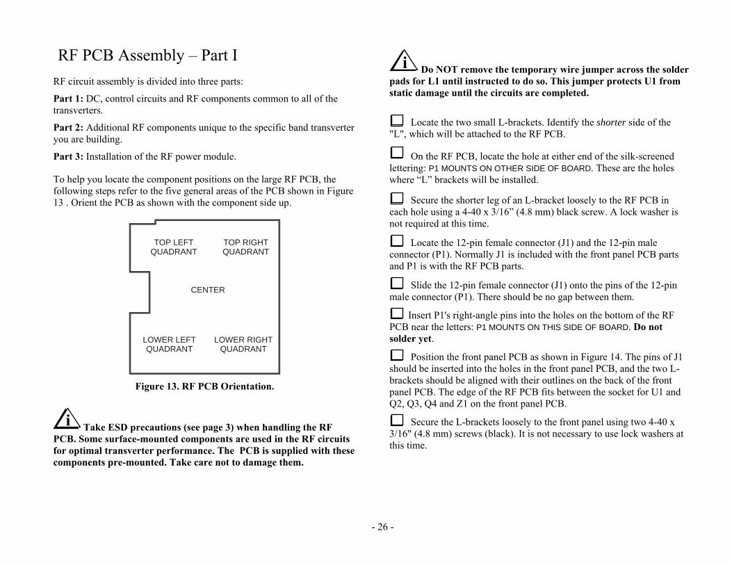
To help you locate the component positions on the large RF PCB, the following steps refer to the five general areas of the PCB shown in Figure 13 . Orient the PCB as shown with the component side up.
TOP LEFTQUADRANT
TOP RIGHTQUADRANT
LOWER LEFTQUADRANT
LOWER RIGHTQUADRANT
CENTER
Figure 13. RF PCB Orientation.
i Take ESD precautions (see page 3) when handling the RF PCB. Some surface-mounted components are used in the RF circuits for optimal transverter performance. The PCB is supplied with these components pre-mounted. Take care not to damage them.
i Do NOT remove the temporary wire jumper across the solder pads for L1 until instructed to do so. This jumper protects U1 from static damage until the circuits are completed.
Locate the two small L-brackets. Identify the shorter side of the "L", which will be attached to the RF PCB.
On the RF PCB, locate the hole at either end of the silk-screened lettering: P1 MOUNTS ON OTHER SIDE OF BOARD. These are the holes where “L” brackets will be installed.
Secure the shorter leg of an L-bracket loosely to the RF PCB in each hole using a 4-40 x 3/16” (4.8 mm) black screw. A lock washer is not required at this time.
Locate the 12-pin female connector (J1) and the 12-pin male connector (P1). Normally J1 is included with the front panel PCB parts and P1 is with the RF PCB parts.
Slide the 12-pin female connector (J1) onto the pins of the 12-pin male connector (P1). There should be no gap between them.
Insert P1's right-angle pins into the holes on the bottom of the RF PCB near the letters: P1 MOUNTS ON THIS SIDE OF BOARD. Do not solder yet.
Position the front panel PCB as shown in Figure 14. The pins of J1 should be inserted into the holes in the front panel PCB, and the two L-brackets should be aligned with their outlines on the back of the front panel PCB. The edge of the RF PCB fits between the socket for U1 and Q2, Q3, Q4 and Z1 on the front panel PCB.
Secure the L-brackets loosely to the front panel using two 4-40 x 3/16" (4.8 mm) screws (black). It is not necessary to use lock washers at this time.

- 27 -
Adjust the L-bracket positions so the front panel PCB is aligned
with the RF PCB. If the gap between the front panel PCB and the RF PCB is wider at one end than the other, you probably have one of the brackets installed backward. Be certain the shorter legs are attached to the RF PCB.
P1
Top of RF board
J1
Figure 14. Installing J1 and P1.
Tighten all four L-bracket screws.
Solder all pins of J1 and P1.
Remove the two screws holding the front panel PCB to the brackets. Unplug the front panel PCB and set it aside in a safe place.
Remove the brackets and screws from the RF PCB and set them aside.
Sort the fixed resistors by wattage and value as follows:
Divide the resistors by wattage: 3-watt (physically largest), 1-watt and 1/4 watt (smallest).
Among the 1/4 watt resistors, separate the four 1% tolerance resistors. These resistors have five color bands: four color bands show the value plus a brown color band at one end that is wider than the others. The wide band indicates that it is a 1% tolerance resistor.
Sort the remaining 1/4 watt resistors by value. If the color bands are difficult to read, use a DMM (digital multimeter) to verify
their values. Tape them to a piece of paper with the values labeled.
Place the PCB with the silk-screened side up and the cutout to your left. The lettering in the center of the PCB will read right side up. All of the remaining parts will be installed on the top, silk-screened side of the PCB.
i Save the longer clipped leads from the following resistors. You will use several of them to make jumpers and test points later.
Install the 1-watt resistors listed below. Space each resistor about 1/16” (1.5 mm) above the PCB by placing the long end of one of the right-angle brackets between the resistor and PCB until the resistor is soldered in place (See Figure 15). The objective is to leave space for air to flow around the resistor. The resistors that should be spaced above the PCB are shown by a double silk screen outline.
R12, 180 ohm (brn-gry-brn), near U1 in the upper left quadrant of the PCB. R16, 120 ohm (brn-red-brn) next to R12. R21, 820 ohms (821), 1 watt next to Q6. R19, 180 ohm (brn-gry-brn), near U5 at the center of the PCB. R8, 120 ohm (brn-red-brn) near Z1 in the lower right quadrant of the PCB.
PLACE RIGHT-ANGLE BRACKET UNDER EACH RESISTOR UNTIL IT IS SOLDERED IN PLACE
SOLDER & TRIM LEADS Figure 15. Spacing the 1-watt and 3-watt Resistors above the PCB.

- 28 -
Install the following 3-watt resistors above R21 near the center of
the PCB. Space each resistor about 1/16” (1.5 mm) above the PCB just like you did for the 1-watt resistors.
__R20, 160 ohm (160) __R26, 160 ohm (160) __R27, 160 ohm (160)
Install the 1/4-watt 1% tolerance resistors listed below in the lower left quadrant of the PCB. Place these and all of the rest of the resistors directly against the PCB.
R35, 5.11k (grn-brn-brn-brn)
R31, 15.0k (brn-grn-blk-red)
R30, 7.5k (vio-grn-blk-brn)
R32, 3.92k (or-wht-red-brn)
Install the 1/4 watt resistors listed below. Start with R1, which is in the upper left quadrant just above the cutout in PCB. The locations follow the perimeter of the PCB going clockwise.
__R1, 10k (brn-blk-org) __R11, 1k (brn-blk-red) __R14, 4.7 ohm (yel-vio-gld) __R23, 100k (brn-blk-yel)
Install the 1/4 watt resistors listed below. Start with R4, which is in the lower right quadrant above Z4. The locations follow the perimeter of the PCB going clockwise.
__R4, 5.6k (grn-blu-red) __R25, 56 ohm (grn-blu-blk) __R5, 5.6K (grn-blu-red) __R7, 10k (brn-blk-org) __R34 (on the right edge of the PCB), 100k (brn-blk-yel) __R9, 10k (brn-blk-org) __R33, 10k (brn-blk-org)
Install the following 1/4 watt resistors next to Q6 at the center of the PCB:
R18, 620 ohm (blu-red-brn)
R40, 22k (red-red-org)
Locate the silk-screened space for D5 on the PCB near R23 in the upper right quadrant of the PCB.
i Diodes must be oriented correctly. A black band around the diode indicates the cathode end. Install each diode so the cathode end goes to the square solder pad and the band is oriented to match the silk-screened outline (see Figure 16 below). If a diode has more than one band, the widest band indicates the cathode end.
Figure 16. PCB Diode Orientation Guides. The cathode always goes
to the square solder pad on the PCB.
Install D5 (SB530) so it is against the PCB and the banded end of the diode is aligned with the banded end of the PCB outline. Save the excess leads when you clip them.
Put the clipped leads from D5 in a safe place. Keep them separate from the other clipped leads you are saving for test points and jumpers. You will use the leads from D5 when you install antenna connector J1 later.
Sort the small glass diodes by type. If necessary use a strong magnifier to read the tiny numbers printed on the glass body. Tape each group to a piece of paper marked by the type number.
1 ea. 1N5235
2 ea. 1N5711
10 ea. 1N4148
- 29 -
Install zener diode D3 (1N5235) in the upper left quadrant of the
PCB near R12. Position it against the PCB with the banded end aligned with the banded end of the PCB outline.
Install the two 1N5711 diodes in the lower right quadrant of the PCB. Place each diode against the PCB with the cathode band oriented as you did in the previous steps.
__D7 __D8
Install the 1N4148 diodes listed below. Start with D1, which is near resistor R1 in the upper left quadrant of the PCB and work clockwise around the PCB.
__D1 __D12 __D6 __D9 __D13 __D14 __D15 __D16 (In lower right quadrant), __D2 __D4
i In the following steps you will install molded inductors. These inductors look much like 1-watt resistors but the color codes read differently. The color codes on the inductors read from the center to the end instead of from the end towards the center like resistors.
Install molded inductor L8, 15H (brn-grn-blk) in the upper right quadrant of the PCB.
Install molded inductor L9, 0.47 H (yel-vio-silver) about half way up the PCB about 2 inches (5 cm) from the right-hand edge.
Install transistor Q6 (PN2222) next to R21 near the center of the PCB. Orient the transistor as shown by the silk-screened outline on the PCB.
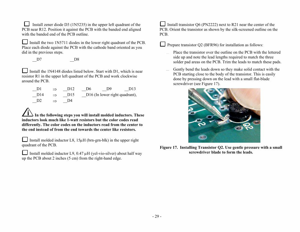
Prepare transistor Q2 (BFR96) for installation as follows:
Place the transistor over the outline on the PCB with the lettered side up and note the lead lengths required to match the three solder pad areas on the PCB. Trim the leads to match these pads.
Gently bend the leads down so they make solid contact with the PCB starting close to the body of the transistor. This is easily done by pressing down on the lead with a small flat-blade screwdriver (see Figure 17).
Figure 17. Installing Transistor Q2. Use gentle pressure with a small
screwdriver blade to form the leads.

- 30 -
Solder Q2 in place as follows:
_ Wet your soldering iron with a small amount of solder and touch it to one lead of Q2 tack-solder it in place.
_ Check alignment of the other two leads to be sure they are over the solder pads. If necessary reheat the tack-soldered lead and adjust the position of the transistor.
_ Solder all three leads properly, soldering the tack-soldered lead last. Keep your soldering time as short as possible to avoid over-heating the transistor. Do not hold the iron on the leads more than two seconds.
i Check each capacitor's labeling carefully to ensure the values agree with the numbers shown in parenthesis.
Install the monolithic capacitors listed below near U3 and Q6 at the center of the PCB.
__C68, .047 F(473) __C67, .01 F (103) __C64, .01F (103) __C65, .047F (473) __C10, .01 F(103) __C9, .01 F (103)
Install the monolithic capacitors listed below. With the PCB oriented with the cutout to the left, start with C62 near the lower left and work around the PCB clockwise to the upper right quadrant.
__C62, .01 F (103) __C40, .01 F (103) __C7, .001 F (102)__C8, .01 F (103) __C3, .001 F (102) __C63, .01F (103)__C6, .01 F (103) __C22, .01 F (103) __C61, .01 F (103)__C2, 100 pF (101) __C23, .01 F (103) __C38, .01 F (103)__C27, .01 F (103) __C29, .047 F(473) __C37, .01 F (103)__C35, 10 pF (100) __C36, F .01 (103) __C34, .01 F (103)__C39, .001 F (102)
Install the monolithic capacitors listed below. Start with C71 on the edge of the PCB in the lower right quadrant and work from right to left across the lower part of the PCB.
__C71,.01 F (103) __C15, .001 F(102) __C16, .01 F (103) __C20, .01 F (103) __C30, 0.22 F(224) __C17, .001 F(102) __C19, .01 F (103) __C57, 100 pF (101)
Install disc ceramic capacitor C18 (2.2) next to C17 in the lower right quadrant of the PCB.
Install the capacitors listed below in the area near the center of the PCB marked 28 MHZ IF BANDPASS FILTER. The lead spacing of these capacitors may be narrower than the hole spacing on the PCB. If necessary, form the leads to avoid stress on the capacitor when they are inserted in the PCB. Do not force the capacitors down against the PCB. The capacitors may sit about 1/16” (1.5 mm) above the PCB as shown in Figure 18 .
__C55, 270 (271) __C54, 150 (151) __C53, 18 (180) or (18) __C52, 150 (151) __C56, 270 (271)
The capacitors shown are typical.
Other styles may be supplied.
Figure 18. Installing I.F. Filter Capacitors.

- 31 -
Use a discarded lead to create test point TP3. Two holes for TP3 are
directly below R17 in the upper right quadrant of the PCB. Bend the lead in a “U” shape and insert it in the holes indicated by a line between them on the PCB. The loop formed should rise about 1/4” (4 mm) above the PCB. Solder the leads.
Use a discarded lead to create TP4 next to TP3, following the procedure described above. Solder the leads.
Make two ground test points just like you did for TP3 and TP4. The places on the PCB are indicated by ground symbols. One is directly below the “Elecraft” label and the other is in the lower left quadrant below U6. Solder the leads.
Remove the eight small relays (G6E-134P) from the carrier tube. If any of the pins are bent, straighten them carefully using long-nose pliers.
i Most likely you’ll want to use a single antenna for both transmitting and receiving with your transverter. However, some operators use separate transmitting and receiving antennas and separate feed lines. The following step provides special instructions to follow only if you are building your transverter for use with separate transmit and receive antennas.
If you are building your transverter for separate (split-path) transmit and receive antenna connections, do the following:
_ In the next step, cross out relay “K1”. It will not be installed. Remove K1 from your parts and set it aside in a safe place. You may want it later if you decide to re-wire your transverter for single antenna operation.
_ Use discarded leads to form jumpers across W2 and W3 near the outline for K1 as shown in Figure 19. Solder them in place.
Figure 19. Installing W2 and W3 for split path (separate transmit
and receive antenna) operation. Do NOT Install Relay K1
Working around the PCB clockwise from the upper left quadrant, place the relays at the following locations. They can only be installed one way. Do not solder the relays yet and do not clip or bend the relay leads.
__K1 __K8 __K9 __K7 __K4 __K5 __K6 __K2
Using a thin, hardcover book to hold the relays in place, flip the PCB and book over together.
Solder just two diagonally opposite corner pins on each relay.
Turn the book back over and check each relay. If any relay is not flat against the PCB, reheat its corner pins while pressing it down against the PCB.
Once all the relays are properly seated, solder the remaining pins. Take care to locate and solder all five pins on every relay. Do not trim the relay pins. Trimming the pins can cause mechanical stress which may reduce the life of the relay.

- 32 -
Install resettable fuse F1 in the space provided next to relay K9 in
the upper right quadrant. F1 may be oriented either way. Solder and trim the leads.
Check the pins on the large relay (KLT1C12DC12). If any pins are bent, straighten them carefully using long-nose pliers.
Install the main power relay K3 (KLT1C12DC12) next to F1 and solder two diagonally opposite corner pins. Check the relay to ensure it is flush against the circuit PCB. If necessary, reheat the solder while pressing down on the relay.
Solder all five pins on relay K3. Do not trim the relay pins. Trimming the pins can cause mechanical stress which may reduce the life of the relay.
Install a 3-terminal header at JP1 adjacent to relay K8. Put a shorting block over two pins of the header to provide a surface where you can place your finger to keep it straight and against the PCB. While holding the assembly, touch one of the pins on the bottom of the PCB with a soldering iron to tack-solder it in place. Check to ensure that the header is sitting vertically on the PCB (see Figure 10 on page 23). Reheat and adjust as necessary, then solder all three pins. Do not hold the solder iron on the pins more than 1 or 2 seconds. Excessive heat will melt the plastic part of the header.
Remove the shorting block from JP1.
Install the following 3-terminal headers: JP2 next to relay K8. JP3 next to relay K8. JP4 near resistor R21. JP5 near relay K6. JP6 near relay K6.
Install JP9 next to K4 and K5. JP9 requires one 2-terminal header and one 3-terminal header.
Install the 100 k-ohm (104) potentiometer R10 (Power Cal) in the upper left quadrant of the PCB. The center lead goes toward the beveled end of the silk screen outline (see Figure 20). The shoulders on the leads should touch the top of the PCB. This pot also may be marked 15K. That is a manufacturer’s mark, not the value.
Figure 20. Installing PC Board Pots. Orient the center pin toward
the beveled end of the silk-screened outline.
Spread the leads on R10, if necessary, to hold it in place, then solder and trim the leads.
Install the two 100 ohm PC board potentiometers just as you did R10:
R13 (101) in the upper left quadrant of the PCB near D3.
R22 (101) below the three 160-ohm 3-watt resistors near the center of the PCB.
Verify that all three terminals on each pot are soldered.

- 33 -
Install 4-pole DIP switch SW1 in the space provided in the lower
left quadrant of the PCB. The DIP switch may not have a notch at one end to line up with the silk-screened outline. Orient the switch so that the ON positions are on the side with the silk-screened numbers. If you aren’t sure, use your DMM to check the orientation of the switch assembly so there is continuity through each switch when the toggle is toward the silk-screened number on the PCB.
Bend the leads of voltage regulator U4 (UA78M05C) to fit on the PCB as shown in Figure 21. Bend the leads around the shaft of a small screwdriver to create smooth rather than sharp bends.
USE SMOOTH BEND
Figure 21. Installing Voltage Regulator U4.
Insert U4’s leads into the holes. Secure it with a zinc or stainless steel 4-40 x 5/16” (8 mm) screw, #4 inside-tooth lock washer and 4-40 nut as shown. The metal tab on the transistor sits directly against the metal foil on the circuit PCB.
Solder all three leads to U4 on the bottom side of the PCB and trim them short.
Locate the two 0.1 F (104), 50V, LS 0.1” Monolithic Ceramic capacitors. These are the capacitors that do not have reference designators in the parts list.
Install the two 0.1 μF (104) capacitors between U4’s center and outer pins as shown in Figure 22. Solder the capacitors directly to U4’s pins with very short leads. Hint: Bend the capacitor leads and hold them with your pliers while tacking one lead onto U4 with your soldering iron carrying a small drop of solder. Then solder the other lead, clean up the first connection if needed, and trim off the excess leads.
Figure 22. Installing the U4 Bypass Capacitors.
Check the resistance between the center pin and each outside pin using your DMM. It must be greater than 500 ohms to confirm no shorts between U4’s pins.
Locate the 10 F, (10) 16V electrolytic capacitor. This is the electrolytic that does not have a reference designator shown on the parts list.
Solder the 10 μF (10) electrolytic capacitor directly to P1 pins 1 (negative) and 2 as shown below using short leads. Be sure to connect the negative (-) lead to pin 1 as shown.
Figure 23. Installing the 10 μF Electrolytic Capacitor on P1.
Check the resistance between P1 pins 1 and 2. It must be greater than 500 ohms to confirm no short between the pins.

- 34 -
Install two 22 F, 25 VDC electrolytic capacitors near the notch on
the left side of the PCB. Be sure to observe polarity. The longer positive lead goes in the square solder pad with a + silk-screened next to it.
__C26 __C60
Locate diodes D10 and D11. They are square, red LEDs identical to the ones you installed on the front panel PCB.
Locate the positions for D10 and D11 on the PCB, near the center on the right hand side. Note that the square solder pad for D10 is to the left and the square solder pad for D11 is to the right. The diodes must be installed turned 180 degrees with respect to each other.
Position diode D10 on the PCB with the long lead through the square pad on the left and the short lead through the round pad. Position the body of the LED directly against the PCB within the silk screen outline and spread the leads under the PCB to hold the diode in place.
Solder one lead on the bottom of the PCB. Check to be sure the LED is still positioned directly against the PCB. Reheat and adjust the LED as necessary, then solder and trim both leads.
Position diode D11 on the PCB with the long lead through the square pad on the right, opposite the orientation of D10. Solder and trim the leads as you did for D10.
Locate the inductors provided for L15, L16 and L17 in the I.F. Bandpass filter. They have grey plastic forms visible inside the shields. Prepare the inductors for installation as follows:
Use the inductor alignment tool to exercise the core in each inductor. If the alignment tool fits tightly, insert it from the bottom to avoid pushing the inductor out of the shield. Run the core up and down through the coil to ensure it runs smoothly (some inductors are very stiff at first) then position the core near the top of the coil.
Check the two leads and the two tabs on the case of each inductor. If they are bent, straighten them carefully using long nose pliers.
Position each inductor on the PCB so that its tabs and pins protrude through on the bottom. The inductors can be positioned either way. Ensure that the shoulders of the tabs are against the top of the PCB, and then bend the tabs toward each other until they are flat on the PCB to hold the inductor in place.
__L16 __L15 __L17
Solder the two tabs and the two pins on all three inductors.
Install voltage regulator U2 (78L09) in the space provided near L17. Be sure to align the body with the silk screen outline on the PCB.
Install transistor Q4 (620) in the space provided near diodes D7 and D8 as shown in Figure 24. Be sure the leads are inserted until their shoulders are against the top of the PCB. If the leads are not inserted far enough, the tab on the top of the transistor may short against the top cover when the cabinet is assembled. Trim the leads as short as possible on the bottom of the PCB.
Figure 24. Installing Transistor Q4.

- 35 -
i The following transistor is particularly sensitive to
electrostatic discharge (ESD) damage. If you are not wearing a grounded antistatic wrist strap, touch an unpainted, grounded object before handling Q5.
Install transistor Q5 (2N7000) in the space provided in the lower right quadrant at the edge of the PCB.
Install two 2-pin header connectors next to Q5.
__JP8 __JP7
Wind toroidal transformer T1 on the FT37-43 (gray) toroid core as follows3. T1 uses a bi-filar winding, which means that two wires are wound on the core together. The wires will be twisted together loosely before they’re wound onto the core.
Twist the red and green enameled wires together over their entire length. The wires should cross over each other 2 to 4 times per inch (1 to 2 times per cm).
Wind 4 turns of the twisted pair on the FT37-43 toroid core as shown in Figure 25 on the next page. Each time the wire passes through the center of the core counts as one turn, so verify that the wires pass through the toroid four times. Spread the turns around the core as shown.
Separate the leads and trim them to a length of about 1” (2.5 cm).
3 A pre-wound toroid is available from an Elecraft-approved source. See page 2.
i In the next step the toroid leads will be stripped and tinned. The leads must be prepared correctly to provide good electrical contact when installed.
Strip the insulation and tin the leads using one of the following techniques:
1. Heat Stripping: a. Place a small amount of solder (a.k.a. a “blob” of solder) on
your soldering iron. b. Insert the clipped end of the wire into the hot solder. If the
iron is hot enough, you should see the insulation bubble and vaporize after 4 to 6 seconds.
c. Add more solder and feed more wire into the solder as the enamel melts. Continue tinning the wire up to the edge of the core, and then slowly pull the wire out of the solder.
d. If any enamel remains on the lead, scrape it away using your thumbnail or sharp tool.
2. Burning: The insulation can be burned off by heating it with a butane lighter for a few seconds. Use sandpaper to remove the residue, then tin the bare wires.
3. Scraping: Use a sharp tool to scrape the insulation away. Work carefully and gently: do not nick the wire. Work around the entire circumference of the wire to remove all of the enamel and tin the bare wires.

- 36 -
Insert the tinned leads in the holes on the PCB and position the
toroid as shown in Figure 25. Be sure the correct lead goes to each hole. Use a magnifier to check the following:
Bare, tinned wire should be visible where the wire enters the hole at the top of the PCB. If necessary remove the toroid and strip the wire further to ensure the wire going through the hole is free of enamel and tinned.
Check carefully for shorts between the wires. The toroid core is not a conductor. Bare wire may touch the core. Be sure that the tinned wires do not touch each other.
Figure 25. Installing T1.
Solder the wires on the bottom of the PCB and trim the leads as short as possible.
Locate the solder pads for choke L7 on the left side of the PCB next to the notch.
Choke L7 consists of a bare wire passing through two ferrite beads as shown in Figure 26. Prepare and install L7 as follows:
Strip the insulation from 3” (7.5 cm) of the #24 solid insulated wire provided.
Bend the wire into a U shape to match the spacing of the holes on the PCB. Place a bead on either side of the bend.
Thread the ends of the wires through the solder pads for L7. Make sure the beads are sitting vertically on the PCB over each hole and bend the leads on the bottom of the PCB to hold the assembly in place.
Solder both leads and trim them as short as possible.
Figure 26. Installing Choke L7.
Install the DPDT power switch at SW2 in the lower right corner of the PCB. Orient the switch so the pushbutton shaft extends out over the edge of the PCB. Be sure the two feet on the bottom of the switch are resting against the PCB before soldering.

- 37 -
Locate the two RCA Jacks, J4 and J5. Use your flush cutters to trim
off the two small plastic feet on each jack (see Figure 27). Be sure they are cut flush so the jacks will sit squarely against the PCB when installed in the next step.
TRIM OFF THE TWO PLASTIC FEET FLUSH WITH THE BOTTOM OF THE JACK.
Figure 27. Preparing the RCA Jacks for Installation.
Install two RCA jacks at the top of the PCB. Solder one pin first then check to be sure the jack is sitting flat against the PCB. If necessary, reheat the solder while pressing down on the jack. Solder the second pin then trim the leads.
__J5 __J4
i J8, installed in the next step, is not required if you are building your transverter to use a common transmit and receive antenna. J8 is needed only if you plan to use separate (split-path) transmit and receive antennas. It won’t hurt to install it in any case.
Install three BNC jacks at the top of the PCB. Line up the two supports and the two small conductor pins with the holes and gently press the connectors down until the four plastic pins on the jack rest directly against the PCB. Solder one of the large pins, then check the position. If necessary, reheat the solder while pressing down on the jack. After soldering all four pins, trim off the excess length of the small pins.
__J8 __J2 __J3
Install the DB-9 connector at J6 and solder the pins including the two larger mounting pins.
The Anderson power connector is held in place by two heavy copper wires soldered to the PCB (See Figure 28). Prepare and install the connector as described in the following steps.
Figure 28. Installing J7.
Cut the length of #14 copper wire provided in half.
Solder each length of the #14 copper wire into the crimp terminal end of an Powerpole® contact. Solder, do not rely on a crimp connection. Take care to keep solder off of the terminal.
Orient each contact as shown in Figure 29 and slide it into a housing until it “clicks” in place. Tug on the wire to be sure it is locked in place. If the contact comes out, you probably have it in upside down.
SPRING#14 WIRE
SOLDERED
TERMINAL LOCKS OVER END OF SPRING
Figure 29. Inserting Contact into Anderson Connector Housing.

- 38 -
Inspect the end of each connector. You should see the contact
pressing up against the end as shown in Figure 30. If necessary, press the contact in from the back until it reaches the end. If you don’t get the contact pushed all the way in so it locks over the end of the spring, it will not make reliable contact with the mating connector.
WRONG RIGHT
Terminal reaches end of
the shell.
Figure 30. Verify Contact is Fully Inserted.
Orient the housings with dimpled side up so that the red and black housings are over the colors marked on the PCB exactly as shown in Figure 31. Be sure the housings are oriented as shown. If they are upside down they will not mate to the connectors on the power cord.
Figure 31. Orienting J7 on the RF PCB.
Look closely at the sides of the housings. Each has a small tongue on one side and a groove on the other. Slide the two housings together engaging the tongue in the groove. Be sure they are fully meshed. No roll pin is needed to lock the shells together.
Bend the copper wire at right angles to the housings so that when it is placed in the holes on the PCB, the housings lie against the PCB within their outline as shown in Figure 31. Be sure the red housing is on the + side and the housings are oriented as shown.
Solder the wires in place and cut them as close to the PCB as possible.
You’ve finished Part I of the RF PCB Assembly Procedure. Go to the RF PCB Assembly – Part II to continue the RF PCB assembly.

- 39 -
RF PCB Assembly – Part II In the following steps you will install components unique to each band on the RF PCB. These components are provided in the XV50, XV144 or XV222 band completion kit package. Perform only the assembly procedure for the transverter you are building.
XV50 – 50 MHz Transverter Perform the following steps on the RF PCB only if you are building the XV50 transverter.
Install resistor R24, 68 ohm (68J), 2 watt, in the lower left quadrant near U6. Space this resistor about 1/16” (1.5 mm) above the PCB like you did the 1-watt and 3-watt resistors earlier (See Figure 15).
Install resistor R6, 330 ohm (org-org-brn), 1/4 watt, above Q2 and U2. Place this resistor directly against the circuit PCB.
Install Z4, a 56 ohm (grn-blu-blk), 1/4 watt resistor near U2.
Install transistor Q1 (NTE108) near U2.
Install the molded inductors listed below:
L2, .22 H (red-red-silver) near U1 in the upper left quadrant of the PCB.
Z3, .15 H (brn-grn-silver) near U6 in the lower left quadrant of the PCB.
L3, .22 H (red-red-silver) near frequency mixer Z1 in the lower right quadrant of the PCB.
Install the following capacitors near transistor Q1: __C12, 100 pF (101) __C14, 390 pF (391)
Install the following capacitors near frequency mixer Z1: __C58, 390 pF (391) __C59, 390 pF (391)
Install capacitor C69, 10 pF (100) near L15 and L16.
Install the two 1-40 pF trimmer capacitors as follows. Align the flat end of each trimmer with the flat end on the silk-screened outline
C33, near L17 on the right lower quadrant of the PCB. (On some PCBs C33 may be marked C64).
C1, to the right relay K1 in the upper left part of the PCB.
Install crystal Y1 where indicated by the silk-screened outline inside circle OV1. The crystal may be oriented either way. Be sure the crystal case is sitting directly on the PCB. Do not hold your soldering iron on the leads more than 2 or 3 seconds maximum. Excessive heat may damage the crystal.
If you purchased the optional crystal oven with your transverter (Elecraft part number E980076) install it now as follows:
Position the oven down over the crystal so the three leads on the oven pass through the +, - , and NC holes in the PCB. The oven will only go on the crystal one way.
Bend the leads over on the bottom of the RF PCB to hold the oven in place, then tack-solder one lead.
Check to be sure the oven fully seated down over the crystal and against the PCB. If necessary, reheat the soldered lead and adjust its position.
Solder and trim all three leads.
Install a jumper across the solder pads for L4A near C13 on the right side of the PCB. Use a discarded lead to make the jumper.
Install voltage regulator U3 (LM78L05) to the left of relay K6 at the center of the PCB.
Install R29, 56 ohm (grn-blu-blk), 1/4 watt, near the center of the PCB.
Install PC trimmer potentiometer R39, 1K ohm (102) near R29.

- 40 -
Install R28, 1k (brn-blk-red), 1/4 watt, near L7 on the left center of the PCB.
Install a jumper across the solder pads at W1 near the notch and electrolytic capacitor C60 on the left side of the PCB.
Wind L10 with 6 turns of #22 enameled wire on the T44-6 (yellow) core as shown in Figure 30. Strip and tin the wires like you did for T1.
REMOVE INSULATIONUP TO THE CORE
THIS LEAD PASSESOVER FRONT OF
CORE
Figure 30. Winding Inductor L10.
Install L10 within the square outline near the upper left corner of the PCB with the leads through the solder pads at the corners of the outline and the toroid sitting upright against the PCB diagonally across the square outline.
Unscrew and remove the tuning slug from L1, the larger gray variable inductor. The tuning slug will not be used.
i If you are not wearing a grounded antistatic wrist strap, touch an unpainted, grounded object before performing the next step. Once the temporary jumper across L1 is removed, Q3 is particularly sensitive to electrostatic discharge (ESD) damage until inductor L1 is soldered in place.
Remove the temporary jumper and install L1 next to trimmer capacitor C1 in the upper left quadrant. Be sure the plastic frame of the inductor is resting against the PCB.
Unscrew and remove the tuning slug from L11, the blue variable inductor. The tuning slug will not be used.
Install L11 near the upper left corner of the PCB. Be sure the plastic frame of the inductor is resting against the PCB.
Locate the shielded inductors with gray inserts provided for L12, L13 and L14. Prepare the inductors for installation as follows:
Use the inductor alignment tool to exercise the core in each inductor. If the alignment tool fits tightly, insert it from the bottom to avoid pushing the inductor out of the shield. Run the core up and down through the coil to ensure it runs smoothly (some inductors are very stiff at first) then position the core near the top of the coil.
Check the two leads and the two tabs on the case of each inductor. If they are bent, straighten them using long nose pliers.
Install the RF Bandpass Filter inductors in the lower right quadrant of the PCB:
__L12 __L13 __L14
Locate the male RCA plug. Solder a jumper between the center pin and the shield. This plug will be used during the alignment procedures.
Carefully inspect the bottom of the PCB for the following: All component leads are soldered. Be especially careful when checking relays and other components with several leads to ensure that all the leads are soldered. There will be some component locations on the PCB that are not filled. This is normal. The same RF PCB is used for the XV50, XV144 and XV222 transverters, and some components are specific to each band. All component leads are clipped at least as short as the relay pins. Do not cut the relay pins.
This finishes Part II of the RF PCB Assembly. Proceed directly to RF PCB Assembly Part III.
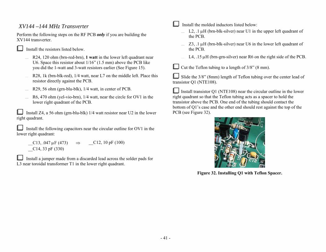
- 41 -
XV144 –144 MHz Transverter
Perform the following steps on the RF PCB only if you are building the XV144 transverter.
Install the resistors listed below.
R24, 120 ohm (brn-red-brn), 1 watt in the lower left quadrant near U6. Space this resistor about 1/16” (1.5 mm) above the PCB like you did the 1-watt and 3-watt resistors earlier (See Figure 15).
R28, 1k (brn-blk-red), 1/4 watt, near L7 on the middle left. Place this resistor directly against the PCB.
R29, 56 ohm (grn-blu-blk), 1/4 watt, in center of PCB.
R6, 470 ohm (yel-vio-brn), 1/4 watt, near the circle for OV1 in the lower right quadrant of the PCB.
Install Z4, a 56 ohm (grn-blu-blk) 1/4 watt resistor near U2 in the lower right quadrant.
Install the following capacitors near the circular outline for OV1 in the lower right quadrant:
__C13, .047 F (473) __C12, 10 pF (100) __C14, 33 pF (330)
Install a jumper made from a discarded lead across the solder pads for L3 near toroidal transformer T1 in the lower right quadrant.
Install the molded inductors listed below: L2, .1 H (brn-blk-silver) near U1 in the upper left quadrant of the PCB.
Z3, .1 H (brn-blk-silver) near U6 in the lower left quadrant of the PCB.
L4, .15 H (brn-grn-silver) near R6 on the right side of the PCB.
Cut the Teflon tubing to a length of 3/8” (8 mm).
Slide the 3/8” (8mm) length of Teflon tubing over the center lead of transistor Q1 (NTE108).
Install transistor Q1 (NTE108) near the circular outline in the lower right quadrant so that the Teflon tubing acts as a spacer to hold the transistor above the PCB. One end of the tubing should contact the bottom of Q1’s case and the other end should rest against the top of the PCB (see Figure 32).
Figure 32. Installing Q1 with Teflon Spacer.

- 42 -
Install crystal Y1 where indicated by the silk-screened outline inside the circular outline for OV1. The crystal may be oriented either way. Be sure the crystal case is sitting directly on the PCB. Do not hold your soldering iron on the leads more than 2 or 3 seconds maximum. Excessive heat may damage the crystal.
If you purchased the optional crystal oven with your transverter (Elecraft part number E980076) install it now as follows:
Position the oven down over the crystal so the three leads on the oven pass through the +, - , and NC holes in the PCB. The oven will only go on the crystal one way.
Bend the leads over on the bottom of the RF PCB to hold the oven in place, then tack-solder one lead.
Check to be sure the oven fully seated down over the crystal and against the PCB. If necessary, reheat the soldered lead and adjust its position.
Solder and trim all three leads.
Install voltage regulator U3 (78L05) to the left of relay K6 at the center of the PCB.
Install PC trimmer potentiometer R39, 1K ohm (102) near the center of the PCB.
Install trimmer capacitor C1, 4-15 pF, to the right of relay K1 in the upper left quadrant of the PCB. This capacitor has a blue dot to identify it.
Remove the tuning slug from L1, the larger variable inductor with an orange plastic frame. The tuning slug will not be used.
i If you are not wearing a grounded antistatic wrist strap, touch an unpainted, grounded object before performing the next step. Once the temporary jumper across L1 is removed, Q3 is particularly sensitive to electrostatic discharge (ESD) damage until inductor L1 is soldered in place.
Remove the temporary jumper across the space for L1 in the upper left quadrant of the PCB and install the orange variable inductor. Be sure the plastic frame of the inductor is resting against the PCB.
Unscrew and remove the tuning slugs from L10 and L11, the smaller orange variable inductors. The tuning slugs will not be used.
Install L10 and L11 near the upper left corner of the PCB. Be sure the plastic frames of the inductors are resting against the PCB.
__L10 __L11
Install L19 (red) near crystal Y1 on the right side of the PCB. Be sure the plastic frame of the inductor is against the PCB.
Adjust the slug in L19 so it is flush with the top of the inductor frame.
Connect the XV144 to your K2 or K3 and apply power prepare to measure the local oscillator frequency tune into a signal of known frequency as described in your XV Owner’s manual under Local Oscillator Frequency Calibration.
Use the K2 or K3 offset (OFS) menu command to correct any frequency error. If the correction required is more than the 9.99 kHz range turn the slug into L19 and retry the offset command. Turning the slug into L19 too far may cause the local oscillator to stop. It may take several iterations to move the local oscillator frequency within range of the offset command.
Measure the voltage between TP1 LO LEVEL and ground while switching the XV144 on and off repeatedly. This voltage is normally between 1.2 and 1.8 VDC. Verify that the voltage returns to the same level each time power is switched on, indicating that the local oscillator is starting reliably.

- 43 -
Locate the shielded inductors with red inserts provided for L12, L13 and L14 in the R.F. Bandpass filter. Prepare the inductors for installation as follows:
Use the inductor alignment tool to exercise the core in each inductor. If the alignment tool fits tightly, insert it from the bottom to avoid pushing the inductor out of the shield. Run the core up and down through the coil to ensure it runs smoothly (some inductors are very stiff at first) then position the core near the top of the coil.
Check the two leads and the two tabs on the case of each inductor. If they are bent, straighten them carefully using long nose pliers.
Install the RF Bandpass Filter inductors in the lower right quadrant:
__L12 __L13 __L14
Install a jumper across the solder pads at W1 near the notch and electrolytic capacitor C60 on the left side of the PCB.
Carefully inspect the bottom of the PCB for the following:
All component leads are soldered. Be especially careful when checking relays and other components with several leads to ensure that all the leads are soldered. There will be some component locations on the PCB that are not filled. This is normal. The same RF PCB is used for the XV50, XV144 and XV222 transverters, and some components are specific to each band.
All component leads are clipped at least as short as the relay leads. Do not cut the relay pins.
Locate the male RCA plug. Solder a jumper between the center pin and the shield. This plug will be used during the Alignment procedures.
This finishes Part II of the RF PCB Assembly. Proceed directly to RF PCB Assembly Part III.

- 44 -
XV222 – 222 MHz Transverter
Perform the following steps on the RF PCB only if you are building the XV222 transverter.
Install the resistors listed below.
R24, 56 ohm (grn-blu-blk), 2 watt, in the lower left quadrant near U6. Space this resistor about 1/16” (1.5 mm) above the PCB like you did the 1-watt and 3-watt resistors earlier (See Figure 15).
R28, 1k (brn-blk-red), 1/4 watt, near L7 on the middle left. Place this resistor directly against the PCB.
R29, 56 ohm (grn-blu-blk), 1/4 watt, in center of PCB.
R6, 220 ohm (red-red-brn), 1/4 watt, above Q2 and U2.
Install Z4, a 56 ohm (grn-blu-blk) 1/4 watt resistor in the lower right quadrant of the PCB.
Install a jumper wire across the solder pads for L3 to the left of toroidal transformer T1 in the lower right quadrant.
Install two .1 H (brn-blk-silver) molded inductors:
L2 near U1 in the upper left quadrant of the PCB.
Z3 near U6 in the lower left quadrant of the PCB.
Install the following capacitors near the circular outline for OV1 in the lower right quadrant:
__C13, .047 F (473) __C12, 15 pF (15) __C14, 22 pF (220)
Cut the Teflon tubing to a length of 3/8” (8mm).
Slide the 3/8” (8mm) length of Teflon tubing over the center lead of transistor Q1 (NTE108).
Install transistor Q1 (NTE108) near U2 so that the Teflon tubing acts as a spacer to hold the transistor above the PCB. One end of the tubing should contact the bottom of Q1’s case and the other end should rest against the top of the circuit PCB (see Figure 33).
Figure 33. Installing Q1 with Teflon Spacer.
Install voltage regulator U3 (78L05) to the left of relay K6 at the center of the PCB.
Install crystal Y1 where indicated by the silk-screened outline inside circle OV1. The crystal may be oriented either way. Be sure the crystal case is sitting directly on the PCB. Do not hold your soldering iron on the leads more than 2 or 3 seconds maximum. Excessive heat may damage the crystal.

- 45 -
If you purchased the optional crystal oven with your transverter (Elecraft part number E980076) install it now as follows:
Position the oven down over the crystal so the three leads on the oven pass through the +, - , and NC holes in the PCB. The oven will only go on the crystal one way.
Bend the leads over on the bottom of the RF PCB to hold the oven in place, then tack-solder one lead.
Check to be sure the oven fully seated down over the crystal and against the PCB. If necessary, reheat the soldered lead and adjust its position.
Solder and trim all three leads.
Install pc pot R39, 1K ohm (102) near the center of the PCB.
Install trimmer capacitor C1, 4-15 pF, to the right of relay K1 at the upper left part of the PCB. This capacitor has a blue dot to identify it.
Adjust the slug in L4A (red plastic frame) so it is flush with the top of the coil form.
Install L4A near crystal Y1 on the right side of the PCB. Be sure its plastic frame is resting against the PCB.
Install L19 near crystal Y1 on the right side of the PCB. Be sure the plastic frame of the inductor is against the PCB.
Unscrew and remove the tuning slug from L1, the larger variable inductor with a brown plastic frame. The tuning slug will not be used.
i If you are not wearing a grounded antistatic wrist strap, touch an unpainted, grounded object before performing the next step. Once the temporary jumper across L1 is removed, Q3 is particularly sensitive to electrostatic discharge (ESD) damage until inductor L1 is soldered in place.
Remove the jumper and install L1 next to trimmer capacitor C1 in the upper left quadrant.
Unscrew and remove the tuning slugs from the two remaining red inductors L10 and L11. The tuning slugs will not be used.
Install the inductors near the upper left corner of the PCB. Be sure the plastic frames of the inductors are resting against the PCB.
__L10 __L11
Locate the shielded inductors with brown inserts provided for L12, L13 and L14 in the R.F. Bandpass filter. Prepare the inductors for installation as follows:
Use the inductor alignment tool to exercise the core in each inductor. If the alignment tool fits tightly, insert it from the bottom to avoid pushing the inductor out of the shield. Run the core up and down through the coil to ensure it runs smoothly (some inductors are very stiff at first) then position the core near the top of the coil.
Check the two leads and the two tabs on the case of each inductor. If they are bent, straighten them carefully using long nose pliers.

- 46 -
Install the RF Bandpass Filter inductors in the spaces provided between relay K2 and frequency mixer Z1:
__L12 __L13 __L14
Install a jumper across the solder pads at W1 on the left side of the PCB near the notch and electrolytic capacitor C60.
Carefully inspect the bottom of the PCB for the following:
All component leads are soldered. Be especially careful when checking relays and other components with several leads to ensure that all the leads are soldered. There will be some component locations on the PCB that are not filled. This is normal. The same RF PCB is used for the XV50, XV144 and XV222 transverters, and some components are specific to each band.
All component leads are clipped at least as short as the relay leads. Do not cut the relay pins.
Locate the male RCA plug. Solder a jumper between the center pin and the shield. This plug will be used during the Alignment procedures.
This finishes Part II of the RF PCB Assembly. Proceed directly to RF PCB Assembly Part III

- 47 -
RF PCB Assembly – Part III In the following steps you will install the RF power module. The procedure is the same for all three transverter models.
If you purchased the optional feet and bail for your transverter, install them on the bottom cover now.
You will use the following small hardware:
14 pan head black screws, 3/16” (4.8 mm) 4-40 thread.
2 pan head black screws, 1/2” (12.7 mm) 4-40 thread.
2 nuts, 4-40 thread.
4 2-D fasteners.
2 flat washers, #4.
2 inside tooth lock washers, #4.
8 split lock washers, #4.
Install four 2-D fasteners on the bottom corners of the RF PCB. Line up the offset holes of each 2-D fastener so the side of the connector is flush with the edge of the PCB (see Figure 34). Secure each connector to the PCB with two black 3/16” (4.8 mm) pan head screws and split lock washers.
HOLES OFFSETFROM CENTER
TOP OFBOARD
LINES UP FLUSHWITH EDGE OF BOARD
CL
Figure 34. 2-D Fasteners.
i In the following steps you will install the hardware that attaches the RF power module to the bottom cover. Follow the steps carefully to ensure the module makes good thermal contact with the bottom cover and the leads line up properly with the RF PCB. The completed hardware assembly is shown in Figure 38 .
Locate the bottom cover. The bottom cover has two sets of cooling holes.
On the inside surface of the bottom cover, locate the four holes that match the holes in the heat spreader. They are between the two sets of cooling holes. Test-fit the larger of the two thermal conduction pads so that the holes in the pad line up with the holes in the cover. Orient the pad so it does not hang over the edge of the bottom cover.
Lift the thermal conduction pad and clean the surface of the bottom cover under the pad using sandpaper, a sharp knife or other tool. The pad must rest against clean, bare metal.
Clean the paint off of the inside surface of the bottom cover around the screw holes in the four corners where the 2-D fasteners will attach it to the RF PCB (See Figure 37).
Inspect the edges of the heat spreader and remove any burrs with the edge of a flat-blade screwdriver, knife or small file.
Replace the larger of the two thermal conduction pads over the clean metal area on the inside of the bottom cover so that the holes line in the pad line up with the holes in the cover. Be sure the pad does not hang over the edge of the bottom cover.
Place the heat spreader on the thermal conduction pad on so the screw holes line up. Put a 1/2” (12.7 mm) pan head screw through each unthreaded hole with the head on the bottom cover. Place a nut on each screw and finger tighten.
Insert two black 3/16” (4.8 mm) pan head screws through the bottom cover into the threaded holes in the head spreader. Tighten the screws.

- 48 -
Lay the bottom cover on a clean, smooth surface with the heat spreader facing up.
Remove the nuts from the long screws but do not remove the screws. If you have installed feet on the bottom cover, place a small book that fits between the feet under the cover so the long screws do not fall out.
Place the smaller thermal conduction pad over the screws. Orient the pad so it does not hang over the edge of the heat spreader.
Position the RF power module on the two screws as shown in Figure 35. Be sure the thermal conduction pad on the heat spreader is resting directly against the bottom of the RF power module.
Place a flat washer on each screw as shown in Figure 35.
Figure 35. RF Power Module and Flat Washers in Place on the Heat
Spreader.
Slide the PCB under the leads on the RF power module and over the screws until they pass through the holes in the PCB (see Figure 36). You can rock the RF Power Module slightly on the screws and bend the leads up as needed to slip the PCB under them and over the tops of the mounting screws.
Place an internal tooth lock washer and nut on each screw and tighten them finger tight.
Figure 36. RF PCB attached to the RF Power Module Screws.
Pick up the entire assembly and secure the four 2-D fasteners to the bottom cover. Each corner is attached with one 3/16” (4.8 mm) black screw (see Figure 37). The other two screw holes in each 2-D fastener will secure the front, rear and side covers in later steps.
Figure 37. Bottom Cover Attached to 2-D Fastener.

- 49 -
Inspect the RF Power module to be sure you have the module and hardware installed exactly as shown in Figure 38.
Figure 38. RF Amplifier Module Mounting Hardware.
Adjust the position of the RF Power module to provide the best alignment of the leads with the solder pads on the PCB. If necessary, loosen the nuts slightly to allow the module to move within the limits of its screw holes.
Hold the RF Power module in place and tighten both screws and nuts to secure it.
i Be sure the four screws holding the RF Power module and heat spreader are tightened securely to ensure good heat transfer. Otherwise the RF Power module may overheat and fail.
Solder the RF power module leads to their corresponding pads on the PCB. Before soldering, trim the leads as needed so they do not extend beyond the solder pads.
This finishes Part III of the RF PCB Assembly. Proceed directly to Final Assembly.

- 50 -
Final AssemblyIn the following steps you’ll finish assembling the transverter.
Remove paint overspray from around the screw holes on the inside surface of the cabinet back panel where the 2-D fasteners will be attached (see Figure 44). The 2-D fasteners should make good electrical contact with the back panel
i Good electrical contact between all of the chassis parts is essential for optimum shielding and system noise figure.
Mount antenna connector J1 on the cabinet back panel using four 5/16” 4-40 pan head zinc or stainless steel screws, lock washers, nuts and one ground lug as shown in Figure 39. Be sure the ground lug is on the lower screw nearest the end of the back panel and faces upward as shown. The antenna connector is an S0-239 (UHF) connector on the XV50 transverter, and a type “N” connector on the XV144 and XV222 transverters.
INSIDE TOOTHLOCK WASHERON EACH SCREW
GROUND LUG ONBOTTOM SCREWNEAREST THE END
Figure 39. Mounting the Antenna Connector J1 on the Back Panel.
Solder the two clipped leads you saved when you installed D5 (Page 28) to the J1 solder pads on the RF PCB. The J1 pads are near K1 (see Figure 40).
Figure 40. J1 Solder Pads on RF PCB.
Position the cabinet back panel on the rear of the RF PCB so the 12 VDC, Control, TXn/IF1, RXout/IF2, Key In and Key Out jacks project through the holes in the cover. Attach the cover to the 2-D fasteners at the rear of the RF PCB using two 3/16” (4.8 mm) black pan head screws.
Attach the two DB-9 male-female standoffs to the Control connector. Use a #4 inside tooth lock washer between each standoff and the rear cover. Note: Do not force the threads. When assembling the modular chassis, screw holes will sometimes not align perfectly. Loosen the other screws holding the panel so it can move as needed to align the holes so all the screws can start easily, then tighten all hardware.
Slip the finish lock washers and nuts over the BNC connectors and tighten them.

- 51 -
Connect J1 to the leads already soldered to the RF PCB as follows (See Figure 41):
_ Solder the lead that is farthest from the edge to the center pin on the antenna connector. This is the lead that goes to the circuit trace on the PCB. Keep the lead as short as possible.
_ Solder the lead attached to the RF PCB at J1 that is closest to the corner to the ground lug on the antenna connector. This is the lead that goes to the ground plane on the PCB. Bend the ground lug as shown to reach it. Keep the lead as short as possible.
Figure 41. Installing J1.
Mount the two right-angle brackets on the edge of the RF PCB (see Figure 14 on page 27). Place the shorter side of each bracket against the top of the RF PCB and secure it with a 3/16” (4.8 mm) screw and split lock washer.
i Either wear a grounded antistatic wrist strap or touch an unpainted, grounded object before handling the processor (U1) in the next steps, or at any time you handle the front panel PCB unplugged from the RF PCB with processor U1 installed.
Remove processor U1 from its conductive foam packing and inspect the pins. The two rows of pins must be straight and parallel to each other to establish the proper pin spacing for insertion into the socket. To straighten the pins, rest one entire row of pins against a hard, flat surface. Press down gently and rock the IC forward to bend the pins into position as shown in Figure 42.
FLARED
STRAIGHT PRESS ANDROCK TOSTRAIGHTEN
Figure 42. Straightening IC Pins.
Identify the end of the IC where Pin 1 is located. It will have a notch, a dimple or both at this end (see Figure 43).
DIMPLE ATPIN 1
NOTCH Figure 43. IC Orientation.

- 52 -
i When U1 is pressed into its socket, you must be careful to avoid jamming its pins. Make sure all the pins are lined up with the associated holes before pressing down on the IC. Watch the pins on both rows as you press down to be sure each pin goes straight down into its socket hole and does not bend in under the IC or outward alongside the socket. Realign each pin individually with its socket hole, if necessary.
Insert processor U1 in its socket with pin 1 or the notched end lined up with the notched end of the socket (the end farthest from the edge of the front panel PCB). Be careful while pressing U6 into its socket not to bend or damage the power indicator LEDs on the front side of the PCB.
Insert plug P1 on the front panel PCB into J1 on the bottom of the RF PCB, and then secure the front panel PCB to the two right angle brackets with 3/16” (4.8 mm) screws and split lock washers.
Place the cabinet front panel face up on your work surface and attach the label with two 2-56 screws. Orient the label with the lighter side upward so that the band identification reads correctly when viewed from the front.
Fit the front panel over the power pushbutton and power LEDs. Attach the front panel to the 2-D fasteners on the bottom of the RF PCB with two 3/16” (4.8 mm) screws.
Press the key cap onto the On/Off switch shaft until it clicks in place.
Attach a 2-D fastener to the each screw hole at the top corners of the front and rear chassis end panels with 3/16” (4.8 mm) screws. Be sure the widest side of each 2-D fastener is facing toward the end of the panel so the edge lines up flush with the edge of the panel as shown in Figure 44.
Figure 44. Attaching 2-D Fasteners to Cabinet End Covers.
Inspect the inside surface of the side covers and remove any paint overspray around the screw holes to ensure good electrical contact with the 2D fasteners.
Attach the side panels using four 3/16” (4.8 mm) screws in each panel. You many need to loosen the other screws holding the end covers temporarily to line up the screw holes properly.
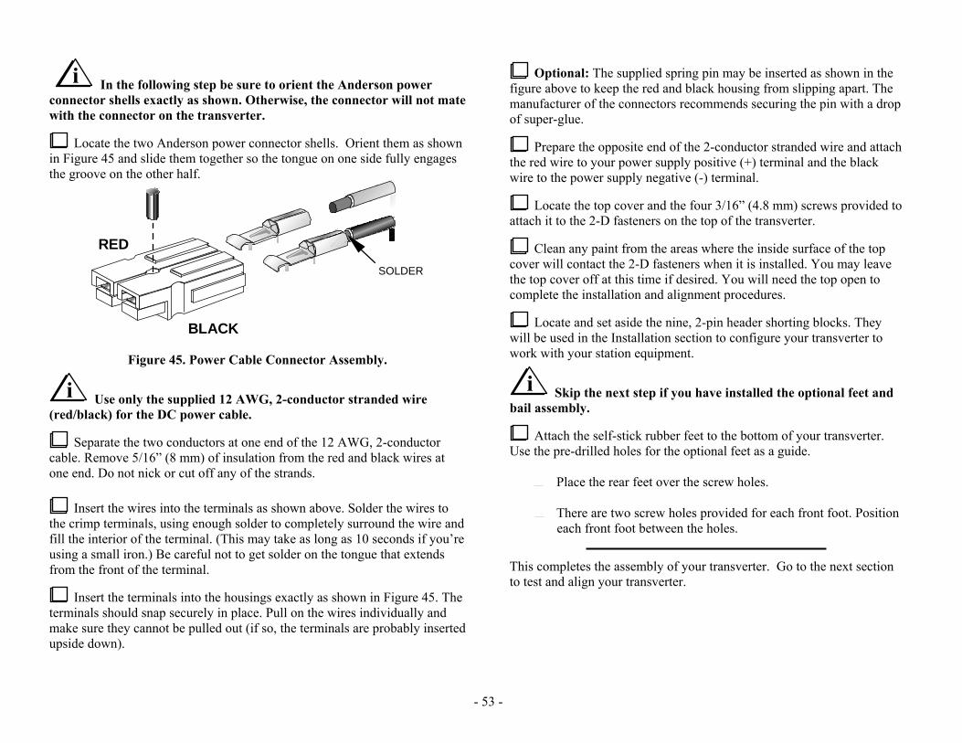
- 53 -
i In the following step be sure to orient the Anderson power connector shells exactly as shown. Otherwise, the connector will not mate with the connector on the transverter.
Locate the two Anderson power connector shells. Orient them as shown in Figure 45 and slide them together so the tongue on one side fully engages the groove on the other half.
BLACK
RED
SOLDER
Figure 45. Power Cable Connector Assembly.
i Use only the supplied 12 AWG, 2-conductor stranded wire (red/black) for the DC power cable.
Separate the two conductors at one end of the 12 AWG, 2-conductor cable. Remove 5/16” (8 mm) of insulation from the red and black wires at one end. Do not nick or cut off any of the strands.
Insert the wires into the terminals as shown above. Solder the wires to the crimp terminals, using enough solder to completely surround the wire and fill the interior of the terminal. (This may take as long as 10 seconds if you’re using a small iron.) Be careful not to get solder on the tongue that extends from the front of the terminal.
Insert the terminals into the housings exactly as shown in Figure 45. The terminals should snap securely in place. Pull on the wires individually and make sure they cannot be pulled out (if so, the terminals are probably inserted upside down).
Optional: The supplied spring pin may be inserted as shown in the figure above to keep the red and black housing from slipping apart. The manufacturer of the connectors recommends securing the pin with a drop of super-glue.
Prepare the opposite end of the 2-conductor stranded wire and attach the red wire to your power supply positive (+) terminal and the black wire to the power supply negative (-) terminal.
Locate the top cover and the four 3/16” (4.8 mm) screws provided to attach it to the 2-D fasteners on the top of the transverter.
Clean any paint from the areas where the inside surface of the top cover will contact the 2-D fasteners when it is installed. You may leave the top cover off at this time if desired. You will need the top open to complete the installation and alignment procedures.
Locate and set aside the nine, 2-pin header shorting blocks. They will be used in the Installation section to configure your transverter to work with your station equipment.
i Skip the next step if you have installed the optional feet and bail assembly.
Attach the self-stick rubber feet to the bottom of your transverter. Use the pre-drilled holes for the optional feet as a guide.
Place the rear feet over the screw holes.
There are two screw holes provided for each front foot. Position each front foot between the holes.
This completes the assembly of your transverter. Go to the next section to test and align your transverter.

- 54 -
Final Test and Alignment In the following steps you will connect your transverter to your station equipment and perform a complete alignment and test procedure.
Turn to the Installation Procedures in your Transverter Owner’s Manual and follow those instructions to connect your transverter to your other station equipment including the rig you will us for a 28 MHz I.F.
Perform the complete Alignment and Test Procedures in your Owner’s Manual to properly adjust and calibrate your transverter and verify that it is operating normally.
If you encounter any difficulties in the alignment and test procedures:
_ Carefully check your setup to ensure all cables are properly connected.
_ Inspect again your parts placement and soldering on the PC PCBs. Most initial difficulties are eventually traced to an incorrectly placed component or a bad solder connection. The circuit description and schematic diagrams in your Owner’s manual can help you decide which circuits to check, based on where in the alignment and test procedures you experience difficulty.
_ Refer to the Troubleshooting information in your Owner’s Manual for nominal voltages at key points in normal operation.
Congratulations You have completed the assembly, test and alignment of your transverter. Turn to your Owner’s Manual for complete installation and operating instructions.
Your Owner’s Manual also describes modifications and optional accessories for your transverter that you may choose to best integrate it with your station equipment.