Embed Size (px)
Citation preview
www.elsevier.com/locate/mee
Microelectronic Engineering 83 (2006) 2462–2468
Assembly and reliability of PBGA packages on FR-4 PCBswith SnAgCu solder
P. Arulvanan a, Z.W. Zhong b,*
a Singapore Institute of Manufacturing Technology, 71 Nanyang Drive, Singapore 638075, Republic of Singaporeb School of Mechanical and Aerospace Engineering, Nanyang Technological University, 50 Nanyang Avenue, Singapore 639798, Republic of Singapore
Received 20 February 2006; received in revised form 26 April 2006; accepted 4 May 2006Available online 21 June 2006
Abstract
Plastic-ball-grid-array (PBGA) packages were assembled onto FR-4 printed-circuit-boards (PCBs) using lead-free SnAgCu solder,different solder pad diameters, stencil thicknesses and reflow peak temperatures, and the effects of the design and assembly process con-ditions on the dimensions and reliability of the solder joints were investigated. The assembled microelectronic devices were subjected to athermal cycling test, and crack initiation and propagation during the test were studied. The results showed that with increased peakreflow temperature and pad diameter, the average joint diameter increased but the average joint height decreased. Increased stencil thick-ness resulted in increased joint diameters and heights. The solder joints consisted of two unique structures of Sn-rich and Ag-rich Sn–Agcompounds. The intermetallic thicknesses were less than 3 lm, and the compounds did not affect the reliability of the solder joints. Fail-ures were not found before 5700 thermal cycles and the characteristic lives of all solder joints were more than 7200 thermal cycles, indi-cating robust solder joints produced with a wide process window.� 2006 Elsevier B.V. All rights reserved.
Keywords: SnAgCu solder joints; Joint dimensions; Thermal cycling; Microstructure; Reliability
1. Introduction
Microelectronic products are used every day in our offi-ces and home. In these products, microelectronic packag-ing plays important roles such as supplying power tointegrated circuit (IC) chips and distributing signals amongmicroelectronic devices. As IC fabrication advances rap-idly, microelectronic packaging faces more and more chal-lenges [1–4].
Solder joints are widely used in microelectronic packag-ing because they can provide mechanical and electrical con-nections and enhance heat spreading efficiency. Thereliability of solder joints is a key issue in the design ofmicroelectronic devices. The reliability problems are largelycaused by the thermal–mechanical stresses in the solderjoints associated with the temperature changes during the
0167-9317/$ - see front matter � 2006 Elsevier B.V. All rights reserved.doi:10.1016/j.mee.2006.05.002
* Corresponding author. Tel.: +65 6790 5588; fax: +65 6791 1859.E-mail address: [email protected] (Z.W. Zhong).
switch-on and -off of a microelectronic device. Predictingthe reliability of solder joints is complicated [5].
Sufficient solderability of the parts used in the solderingprocess is a major prerequisite for the success of the process[6]. Good solderability results in good wetting, whichmeans the formation of a uniform, smooth, unbroken,adherent coat of solder on the base metal, without theuse of highly active fluxes and impairing the function ofthe parts soldered.
The increasing need to measure material properties ofmicroscopic structures requires suitable techniques forstrain measurements [7]. To evaluate the reliability perfor-mance of solder joints in microelectronic devices, variousreliability tests are performed, which are time-consuming[8,9]. Therefore, another approach becomes popular anduseful, which is to predict the fatigue life by simulatingand analyzing the deformations, stresses and strains ofmicroelectronics packages using finite element methods[10,11]. However, experimental methods are highly needed
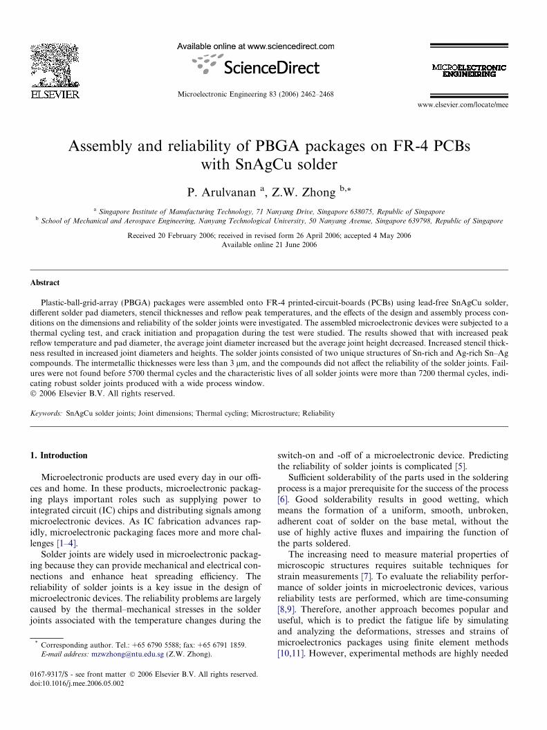
Fig. 1. Lead-free 352-ball PBGA.
P. Arulvanan, Z.W. Zhong / Microelectronic Engineering 83 (2006) 2462–2468 2463
to verify the deformations and strains obtained from thenumerical simulations. One of such experimental methodsis to measure deformations and strains in solder jointsusing a Moire method [12,13]. Various methods to inspectsolder joints have also been developed [14,15]. It has beenfound that interfacial preexisting voids can accelerate elec-tromigration failures, which can reduce over a half of thesolder joint lifetime with a 20% volume fraction of interfa-cial voids [16].
The components of the tin–lead system are completelysoluble in the liquid state but only partially soluble in thesolid state. This is the most common type of binary systemsand is the same as for the systems of copper–silver, copper–tin, copper–zinc, aluminum–copper and aluminum–magne-sium [17].
Tin–lead solders have been widely used to make micro-electronic interconnections for decades. Their materialproperties and mathematical models for reliability predic-tion and the behavior of tin–lead solder joints are knownreadily.
With more microelectronic products required to be envi-ronmentally friendly, research on lead-free solder hasbecome an urgent task for the microelectronic packagingindustry [18]. Environmental concerns and legal constraints[19] have been pushing to replace tin–lead solders withlead-free solders or adhesives [20] in manufacturing ofmicroelectronic devices. However, a great deal of reliabilitytests for lead-free solder joints are needed before they canreplace traditional tin–lead solders [21]. Therefore, variouslead-free alloys including binary, ternary and quaternarysolders are being evaluated for use in printed circuit board(PCB) assemblies. For material and process data, lead-freesolder interconnections are lacking and as such research isbeing conducted worldwide.
One of the most promising materials to replace tin–leadsolders is SnAgCu [22]. There are three phases in theSnAgCu eutectic material, bSn and the intermetallics ofAg3Sn and Cu6Sn5. The equilibrium point between Ag3Snand Cu6Sn5 is at 225 �C. The theoretical true eutectic pointfor the SnAgCu system lies at Sn3.4Ag0.7Cu [23].
Investigation of ball-grid-array (BGA) components withSn3.8Ag0.7Cu alloy solder balls found an intermetallicinterface of SnNiCu on NiAu PCB pads after a thermalcycling test (�55 �C to +125 �C). The solder joint failuresstarted occurring before 2000 cycles of the thermal cyclingtest [24]. Lead-free solder joints have fine and stable micro-structures due to formation of small-dispersed particles andconsequently higher shear strengths than tin–lead solders[25]. Microstructures of Sn and plate like Ag3Sn wereobserved with dendritic Sn phase for Sn3.0Ag0.5Cu alloysincluding Cu6Sn5 in SnAgCu eutectics [26]. The Ni3Sn4
intermetallic was found uniform and thin inSn3.5Ag0.5Cu, while it was thick and less regular inSn4.0Ag0.5Cu under dual reflow conditions using electro-less Ni–P for BGA assemblies [27].
This work attempted to study the effects of design andassembly process conditions on lead-free SnAgCu solder
joints. The process variables studied include solder paddiameters, stencil thicknesses and reflow peak tempera-tures. Experiments using SnAgCu solder for assemblingplastic-ball-grid-array (PBGA) packages on PCBs wereperformed to investigate the reliability of the lead-free sol-der joints made under various conditions.
2. Assembly matrix and materials
Fig. 1 shows the PBGA package of 35 mm · 35 mm with352 Sn4.0Ag0.5Cu balls assembled in this work. PCBs weredesigned with daisy chain loops along the outer rows ofsolder balls of the PBGA packages. They were fabricatedwith a high Tg (170 �C) FR-4 material having electrolessnickel-immersion gold (NiAu) finish, and had dimensionsof 150 mm · 212 mm. The daisy chains on the outerperiphery of the package were routed through a PCB daisychain designed to meet the in situ measurement require-ments of the thermal-cycling chamber. The boards had atotal of 12 resistance loops (one loop per package) moni-tored for electrical continuity during temperature cycletesting. The non-solder-mask-defined (NSMD) pads hadan opening diameter of 0.66 mm on one side of the PCBand on the other side had an opening diameter of0.56 mm. The pad sizes of 0.56 and 0.66 mm were chosento study the effect of the variation in standoff heights onthe reliability of lead-free solder joints. Before assembly,material characterization, reflow oven profiling and processvalidation were performed to evaluate the quality of indi-vidual components.
The PBGA packages were assembled on one side of thePCBs with Sn3.5Ag0.7Cu solder paste according to theassembly matrix shown in Table 1. Two stencils werefabricated with the same pad-opening area(0.56 mm · 0.56 mm) but different thicknesses. The pastevolume on the solder pads of the PCBs was controlled
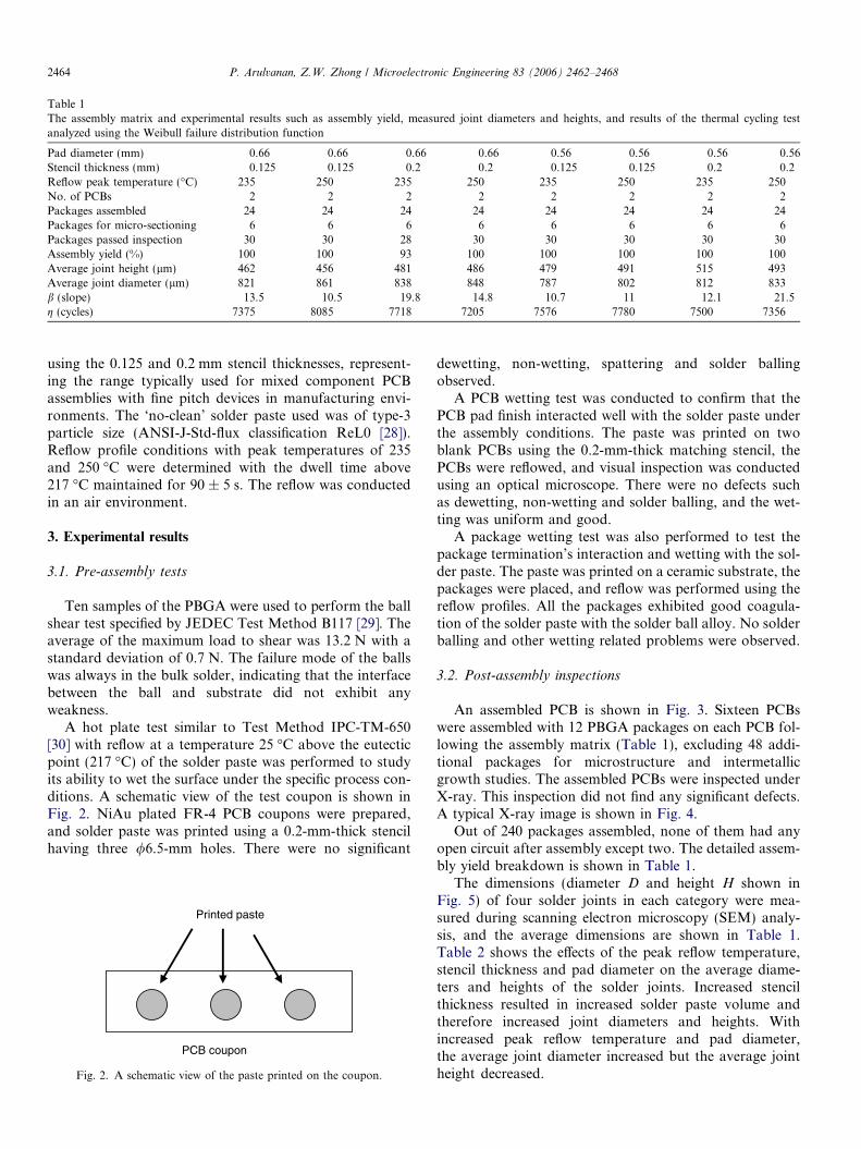
Table 1The assembly matrix and experimental results such as assembly yield, measured joint diameters and heights, and results of the thermal cycling testanalyzed using the Weibull failure distribution function
Pad diameter (mm) 0.66 0.66 0.66 0.66 0.56 0.56 0.56 0.56Stencil thickness (mm) 0.125 0.125 0.2 0.2 0.125 0.125 0.2 0.2Reflow peak temperature (�C) 235 250 235 250 235 250 235 250No. of PCBs 2 2 2 2 2 2 2 2Packages assembled 24 24 24 24 24 24 24 24Packages for micro-sectioning 6 6 6 6 6 6 6 6Packages passed inspection 30 30 28 30 30 30 30 30Assembly yield (%) 100 100 93 100 100 100 100 100Average joint height (lm) 462 456 481 486 479 491 515 493Average joint diameter (lm) 821 861 838 848 787 802 812 833b (slope) 13.5 10.5 19.8 14.8 10.7 11 12.1 21.5g (cycles) 7375 8085 7718 7205 7576 7780 7500 7356
2464 P. Arulvanan, Z.W. Zhong / Microelectronic Engineering 83 (2006) 2462–2468
using the 0.125 and 0.2 mm stencil thicknesses, represent-ing the range typically used for mixed component PCBassemblies with fine pitch devices in manufacturing envi-ronments. The ‘no-clean’ solder paste used was of type-3particle size (ANSI-J-Std-flux classification ReL0 [28]).Reflow profile conditions with peak temperatures of 235and 250 �C were determined with the dwell time above217 �C maintained for 90 ± 5 s. The reflow was conductedin an air environment.
3. Experimental results
3.1. Pre-assembly tests
Ten samples of the PBGA were used to perform the ballshear test specified by JEDEC Test Method B117 [29]. Theaverage of the maximum load to shear was 13.2 N with astandard deviation of 0.7 N. The failure mode of the ballswas always in the bulk solder, indicating that the interfacebetween the ball and substrate did not exhibit anyweakness.
A hot plate test similar to Test Method IPC-TM-650[30] with reflow at a temperature 25 �C above the eutecticpoint (217 �C) of the solder paste was performed to studyits ability to wet the surface under the specific process con-ditions. A schematic view of the test coupon is shown inFig. 2. NiAu plated FR-4 PCB coupons were prepared,and solder paste was printed using a 0.2-mm-thick stencilhaving three /6.5-mm holes. There were no significant
PCB coupon
Printed paste
Fig. 2. A schematic view of the paste printed on the coupon.
dewetting, non-wetting, spattering and solder ballingobserved.
A PCB wetting test was conducted to confirm that thePCB pad finish interacted well with the solder paste underthe assembly conditions. The paste was printed on twoblank PCBs using the 0.2-mm-thick matching stencil, thePCBs were reflowed, and visual inspection was conductedusing an optical microscope. There were no defects suchas dewetting, non-wetting and solder balling, and the wet-ting was uniform and good.
A package wetting test was also performed to test thepackage termination’s interaction and wetting with the sol-der paste. The paste was printed on a ceramic substrate, thepackages were placed, and reflow was performed using thereflow profiles. All the packages exhibited good coagula-tion of the solder paste with the solder ball alloy. No solderballing and other wetting related problems were observed.
3.2. Post-assembly inspections
An assembled PCB is shown in Fig. 3. Sixteen PCBswere assembled with 12 PBGA packages on each PCB fol-lowing the assembly matrix (Table 1), excluding 48 addi-tional packages for microstructure and intermetallicgrowth studies. The assembled PCBs were inspected underX-ray. This inspection did not find any significant defects.A typical X-ray image is shown in Fig. 4.
Out of 240 packages assembled, none of them had anyopen circuit after assembly except two. The detailed assem-bly yield breakdown is shown in Table 1.
The dimensions (diameter D and height H shown inFig. 5) of four solder joints in each category were mea-sured during scanning electron microscopy (SEM) analy-sis, and the average dimensions are shown in Table 1.Table 2 shows the effects of the peak reflow temperature,stencil thickness and pad diameter on the average diame-ters and heights of the solder joints. Increased stencilthickness resulted in increased solder paste volume andtherefore increased joint diameters and heights. Withincreased peak reflow temperature and pad diameter,the average joint diameter increased but the average jointheight decreased.
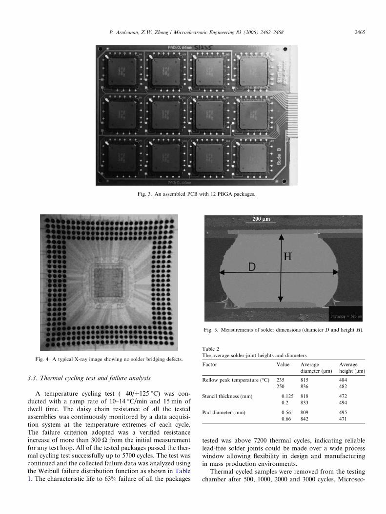
Fig. 3. An assembled PCB with 12 PBGA packages.
Fig. 4. A typical X-ray image showing no solder bridging defects.
Fig. 5. Measurements of solder dimensions (diameter D and height H).
Table 2The average solder-joint heights and diameters
Factor Value Averagediameter (lm)
Averageheight (lm)
Reflow peak temperature (�C) 235 815 484250 836 482
Stencil thickness (mm) 0.125 818 4720.2 833 494
Pad diameter (mm) 0.56 809 4950.66 842 471
P. Arulvanan, Z.W. Zhong / Microelectronic Engineering 83 (2006) 2462–2468 2465
3.3. Thermal cycling test and failure analysis
A temperature cycling test (�40/+125 �C) was con-ducted with a ramp rate of 10–14 �C/min and 15 min ofdwell time. The daisy chain resistance of all the testedassemblies was continuously monitored by a data acquisi-tion system at the temperature extremes of each cycle.The failure criterion adopted was a verified resistanceincrease of more than 300 X from the initial measurementfor any test loop. All of the tested packages passed the ther-mal cycling test successfully up to 5700 cycles. The test wascontinued and the collected failure data was analyzed usingthe Weibull failure distribution function as shown in Table1. The characteristic life to 63% failure of all the packages
tested was above 7200 thermal cycles, indicating reliablelead-free solder joints could be made over a wide processwindow allowing flexibility in design and manufacturingin mass production environments.
Thermal cycled samples were removed from the testingchamber after 500, 1000, 2000 and 3000 cycles. Microsec-
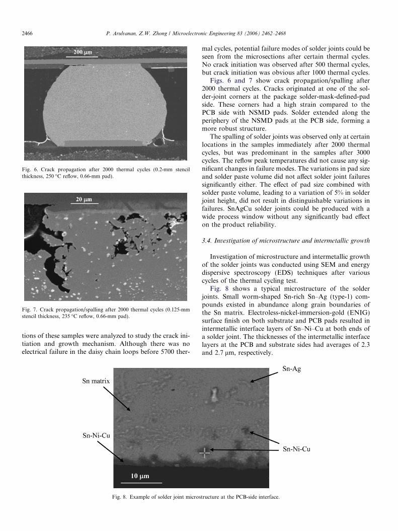
Fig. 6. Crack propagation after 2000 thermal cycles (0.2-mm stencilthickness, 250 �C reflow, 0.66-mm pad).
Fig. 7. Crack propagation/spalling after 2000 thermal cycles (0.125-mmstencil thickness, 235 �C reflow, 0.66-mm pad).
2466 P. Arulvanan, Z.W. Zhong / Microelectronic Engineering 83 (2006) 2462–2468
tions of these samples were analyzed to study the crack ini-tiation and growth mechanism. Although there was noelectrical failure in the daisy chain loops before 5700 ther-
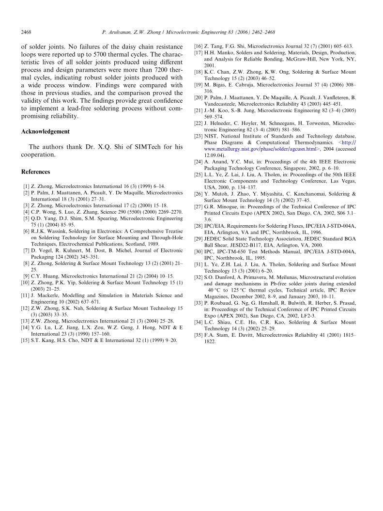
Fig. 8. Example of solder joint micros
mal cycles, potential failure modes of solder joints could beseen from the microsections after certain thermal cycles.No crack initiation was observed after 500 thermal cycles,but crack initiation was obvious after 1000 thermal cycles.
Figs. 6 and 7 show crack propagation/spalling after2000 thermal cycles. Cracks originated at one of the sol-der-joint corners at the package solder-mask-defined-padside. These corners had a high strain compared to thePCB side with NSMD pads. Solder extended along theperiphery of the NSMD pads at the PCB side, forming amore robust structure.
The spalling of solder joints was observed only at certainlocations in the samples immediately after 2000 thermalcycles, but was predominant in the samples after 3000cycles. The reflow peak temperatures did not cause any sig-nificant changes in failure modes. The variations in pad sizeand solder paste volume did not affect solder joint failuressignificantly either. The effect of pad size combined withsolder paste volume, leading to a variation of 5% in solderjoint height, did not result in distinguishable variations infailures. SnAgCu solder joints could be produced with awide process window without any significantly bad effecton the product reliability.
3.4. Investigation of microstructure and intermetallic growth
Investigation of microstructure and intermetallic growthof the solder joints was conducted using SEM and energydispersive spectroscopy (EDS) techniques after variouscycles of the thermal cycling test.
Fig. 8 shows a typical microstructure of the solderjoints. Small worm-shaped Sn-rich Sn–Ag (type-1) com-pounds existed in abundance along grain boundaries ofthe Sn matrix. Electroless-nickel-immersion-gold (ENIG)surface finish on both substrate and PCB pads resulted inintermetallic interface layers of Sn–Ni–Cu at both ends ofa solder joint. The thicknesses of the intermetallic interfacelayers at the PCB and substrate sides had averages of 2.3and 2.7 lm, respectively.
tructure at the PCB-side interface.
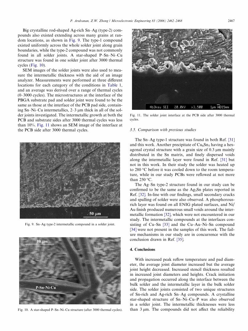
Fig. 11. The solder joint interface at the PCB side after 3000 thermalcycles.
P. Arulvanan, Z.W. Zhong / Microelectronic Engineering 83 (2006) 2462–2468 2467
Big crystalline rod-shaped Ag-rich Sn–Ag (type-2) com-pounds also existed extending across many grains at ran-dom locations, as shown in Fig. 9. The type-1 compoundexisted uniformly across the whole solder joint along grainboundaries, while the type-2 compound was not commonlyfound in all solder joints. A star-shaped P–Sn–Ni–Custructure was found in one solder joint after 3000 thermalcycles (Fig. 10).
SEM images of the solder joints were also used to mea-sure the intermetallic thickness with the aid of an imageanalyzer. Measurements were performed at three differentlocations for each category of the conditions in Table 1,and an average was derived over a range of thermal cycles(0–3000 cycles). The microstructures at the interface of thePBGA substrate pad and solder joint were found to be thesame as those at the interface of the PCB pad side, contain-ing Sn–Ni–Cu intermetallics, 2–3 lm thick in all of the sol-der joints investigated. The intermetallic growth at both thePCB and substrate sides after 3000 thermal cycles was lessthan 10%. Fig. 11 shows an SEM image of the interface atthe PCB side after 3000 thermal cycles.
Fig. 10. A star-shaped P–Sn–Ni–Cu structure (after 3000 thermal cycles).
Fig. 9. Sn–Ag type-2 intermetallic compound in a solder joint.
3.5. Comparison with previous studies
The Sn–Ag type-1 structure was found in both Ref. [31]and this work. Another precipitate of Cu6Sn5 having a hex-agonal crystal structure with a grain size of 0.3 lm mainlydistributed in the Sn matrix, and finely dispersed voidsalong the intermetallic layer were found in Ref. [31] butnot in this work. In their study the solder was heated upto 280 �C before it was cooled down to the room tempera-ture, while in our study PCBs were reflowed at not morethan 250 �C.
The Ag–Sn type-2 structure found in our study can beconfirmed to be the same as the Ag3Sn plates reported inRef. [32]. In-line with our findings, small secondary cracksand spalling of solder were also observed. A phosphorous-rich layer was found on all ENIG plated surfaces, and Ni/Au finish produced numerous small voids around the inter-metallic formation [32], which were not encountered in ourstudy. The intermetallic compounds at the interfaces con-sisting of Cu–Sn [33] and the Cu–Au–Ni–Sn compound[34] were not present in the samples of this work. The fail-ure mechanisms in our study are in concurrence with theconclusion drawn in Ref. [35].
4. Conclusions
With increased peak reflow temperature and pad diam-eter, the average joint diameter increased but the averagejoint height decreased. Increased stencil thickness resultedin increased joint diameters and heights. Crack initiationand propagation occurred along the interface between thebulk solder and the intermetallic layer in the bulk solderside. The solder joints consisted of two unique structuresof Sn-rich and Ag-rich Sn–Ag compounds. A crystallinestar-shaped structure of Sn–Ni–Cu–P was also observedin a solder joint. The intermetallic thicknesses were lessthan 3 lm. The compounds did not affect the reliability
2468 P. Arulvanan, Z.W. Zhong / Microelectronic Engineering 83 (2006) 2462–2468
of solder joints. No failures of the daisy chain resistanceloops were reported up to 5700 thermal cycles. The charac-teristic lives of all solder joints produced using differentprocess and design parameters were more than 7200 ther-mal cycles, indicating robust solder joints produced witha wide process window. Findings were compared withthose in previous studies, and the comparison proved thevalidity of this work. The findings provide great confidenceto implement a lead-free soldering process without com-promising reliability.
Acknowledgement
The authors thank Dr. X.Q. Shi of SIMTech for hiscooperation.
References
[1] Z. Zhong, Microelectronics International 16 (3) (1999) 6–14.[2] P. Palm, J. Maattanen, A. Picault, Y. De Maquille, Microelectronics
International 18 (3) (2001) 27–31.[3] Z. Zhong, Microelectronics International 17 (2) (2000) 15–18.[4] C.P. Wong, S. Luo, Z. Zhang, Science 290 (5500) (2000) 2269–2270.[5] Q.D. Yang, D.J. Shim, S.M. Spearing, Microelectronic Engineering
75 (1) (2004) 85–95.[6] R.J.K. Wassink, Soldering in Electronics: A Comprehensive Treatise
on Soldering Technology for Surface Mounting and Through-HoleTechniques, Electrochemical Publications, Scotland, 1989.
[7] D. Vogel, R. Kuhnert, M. Dost, B. Michel, Journal of ElectronicPackaging 124 (2002) 345–351.
[8] Z. Zhong, Soldering & Surface Mount Technology 13 (2) (2001) 21–25.
[9] C.Y. Huang, Microelectronics International 21 (2) (2004) 10–15.[10] Z. Zhong, P.K. Yip, Soldering & Surface Mount Technology 15 (1)
(2003) 21–25.[11] J. Mackerle, Modelling and Simulation in Materials Science and
Engineering 10 (2002) 637–671.[12] Z.W. Zhong, S.K. Nah, Soldering & Surface Mount Technology 15
(3) (2003) 33–35.[13] Z.W. Zhong, Microelectronics International 21 (3) (2004) 25–28.[14] Y.G. Lu, L.Z. Jiang, L.X. Zou, W.Z. Geng, J. Hong, NDT & E
International 23 (3) (1990) 157–160.[15] S.T. Kang, H.S. Cho, NDT & E International 32 (1) (1999) 9–20.
[16] Z. Tang, F.G. Shi, Microelectronics Journal 32 (7) (2001) 605–613.[17] H.H. Manko, Solders and Soldering, Materials, Design, Production,
and Analysis for Reliable Bonding, McGraw-Hill, New York, NY,2001.
[18] K.C. Chan, Z.W. Zhong, K.W. Ong, Soldering & Surface MountTechnology 15 (2) (2003) 46–52.
[19] M. Bigas, E. Cabruja, Microelectronics Journal 37 (4) (2006) 308–316.
[20] P. Palm, J. Maattanen, Y. De Maquille, A. Picault, J. Vanfleteren, B.Vandecasteele, Microelectronics Reliability 43 (2003) 445–451.
[21] J.-M. Koo, S.-B. Jung, Microelectronic Engineering 82 (3–4) (2005)569–574.
[22] J. Helneder, C. Hoyler, M. Schneegans, H. Torwesten, Microelec-tronic Engineering 82 (3–4) (2005) 581–586.
[23] NIST, National Institute of Standards and Technology database,Phase Diagrams & Computational Thermodynamics. <http://www.metallurgy.nist.gov/phase/solder/agcusn.html>, 2004 (accessed12.09.04).
[24] A. Anand, Y.C. Mui, in: Proceedings of the 4th IEEE ElectronicPackaging Technology Conference, Singapore, 2002, p. 6–10.
[25] L.L. Ye, Z. Lai, J. Liu, A. Tholen, in: Proceedings of the 50th IEEEElectronic Components and Technology Conference, Las Vegas,USA, 2000, p. 134–137.
[26] Y. Mutoh, J. Zhao, Y. Miyashita, C. Kanchanomai, Soldering &Surface Mount Technology 14 (3) (2002) 37–45.
[27] G.R. Minogue, in: Proceedings of the Technical Conference of IPCPrinted Circuits Expo (APEX 2002), San Diego, CA, 2002, S06 3.1–3.6.
[28] IPC/EIA, Requirements for Soldering Fluxes, IPC/EIA J-STD-004A,EIA, Arlington, VA and IPC, Northbrook, IL, 1996.
[29] JEDEC Solid State Technology Association, JEDEC Standard BGABall Shear, JESD22-B117, EIA, Arlington, VA, 2000.
[30] IPC, IPC-TM-650 Test Methods Manual, IPC/EIA J-STD-004A,IPC, Northbrook, IL, 1995.
[31] L. Ye, Z.H. Lai, J. Liu, A. Tholen, Soldering and Surface MountTechnology 13 (3) (2001) 6–20.
[32] S.O. Dunford, A. Primavera, M. Meilunas, Microstructural evolutionand damage mechanisms in Pb-free solder joints during extended�40 �C to 125 �C thermal cycles, Technical article, IPC ReviewMagazines, December 2002, 8–9, and January 2003, 10–11.
[33] P. Roubaud, G. Ng, G. Henshall, R. Bulwith, R. Herber, S. Prasad,in: Proceedings of the Technical Conference of IPC Printed CircuitsExpo (APEX 2002), San Diego, CA, 2002, LF2-3.
[34] L.C. Shiau, C.E. Ho, C.R. Kao, Soldering & Surface MountTechnology 14 (3) (2002) 25–29.
[35] F.A. Stam, E. Davitt, Microelectronics Reliability 41 (2001) 1815–1822.


![Burn-in & Test Socket Workshop · Testing Lead Free Area Array Packages BiTS 2003 19 PBGA Contactor Resistance at Burnin [1.27mm] • Burn-in Parameters – Pinch style BGA socket](https://img.pdfslide.us/doc/110x75/6082d0b9111a4960bc2e8acc/burn-in-test-socket-workshop-testing-lead-free-area-array-packages-bits-2003.jpg)