Embed Size (px)
Citation preview
AS8221D FlexRay Standard Transceiver
Objective Data Sheet
1 General DescriptionThis objective data sheet describes the intended functionality of the AS8221 bus transceiver. As long the device is not fully qualified, the parameters are not characterized in the means that parameters may change or can be updated during final product qualification and characterization. This document shows the objective of the AS8221 and this document is subjected to change without notice.
The AS8221 is a high speed automotive bus driver designed according to the FlexRay Electrical Physical Layer Specification V2.1 Rev B. The AS8221 operates as a bi-directional interface between the FlexRay Communication Controller and the twisted-pair copper wiring.
The AS8221 provides an optimized host controller interface consisting of three low-active pins. The Enable and Standby input pins for mode handling by the microcontroller and the Error out pin where system, chip failures or status information are signalled to the microcontroller. Signalling logic high on the Enable and Standby pin the device will enter Normal mode in case no fault condition is given and in this mode the device is fully operational meaning FlexRay communication is possible. Additionally a Receive Only mode is implemented, which can be accessed by the microcontroller where only FlexRay streams can be received in order to avoid unwanted disturbances on the FlexRay bus while listening on the bus traffic. In the low power modes (Standby and Sleep mode) very low power consumption is achieved.
In case of undervoltage on one of the supply voltages (VBAT, VCCand VIO) the device will change its mode to a low power mode (either Standby or Sleep mode) and the device will signal an error accordingly. In case of low voltage is detected on both VBAT and VCC the device will enter the Power Off mode, where no operation is possible. A safe mechanism from the low power modes to Power Off mode and vice versa is implemented ensuring that no deadlock can happen during the startup phase.
Ensuring application in safety critical environments a two wire bus-guardian interface is implemented where additional monitoring circuitries on the electronic-control-unit can activate and deactivate the transmitter and additionally on the receive enable output in low power modes the wake conditions and in normal power modes the received FlexRay streams can be monitored.
A thermal sensor circuit with an integral shutdown mechanism prevents damage to the device in extreme temperature conditions. The symmetrical transient control for the high- and low-side driver for both the bus-minus and bus-plus line allows an ideal balance of communications over different network topologies, with excellent EMC performance.
2 Key Features Compliant with FlexRay Electrical Physical Layer
Specification V2.1 Rev. B Data transfer up to 10 Mbps Excellent EMC performances. High common mode
range insure excellent EMI Interface for Bus Guardian or supervision circuits Automatic thermal shutdown protection Supports 12V and 24V systems with very low sleep
current Integrated power management system
- Two inhibit pins for external voltage supply control- Local wake-up input- Remote wake-up capability via FlexRay bus in low
power modes Supports 2.5, 3, 3.3, 5 V microcontrollers and
automatically adapts to interface levels Protection against damage due to short circuit
conditions on the bus (positive and negative battery voltage) Operating temperature range -40ºC to +125ºC Lead-free SSOP20 package
3 ApplicationsThe AS8221 FlexRay Standard Transceiver is best fitting for all automotive applications where the full functionality of the FlexRay bus driver is needed in the electronic-control-unit like bus wake-up and control for voltage supplies.
The device addresses all ECUs connected to the permanent battery supply (clamp 30). The AS8221 is connected to the battery voltage and therefore can be used as the only ECU wake-up component with very low power consumption in Sleep mode.
www.austriamicrosystems.com Revision 17732-005-10a 1 - 44
AS8221Objective Data Sheet - App l i ca t ions
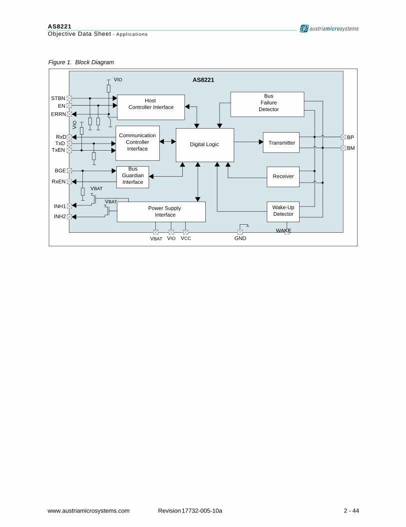
Figure 1. Block Diagram
Host Controller Interface
BusFailure
Detector
Communication ControllerInterface
BusGuardianInterface
Power Supply Interface
Wake-UpDetector
Receiver
TransmitterDigital Logic
AS8221
STBNEN
ERRN
RxDTxD
TxEN
BGE
RxEN
INH1
INH2
VBAT VIO VCC GNDWAKE
BM
BP
VIOV
IO
VBAT
VBAT
www.austriamicrosystems.com Revision 17732-005-10a 2 - 44
AS8221Objective Data Sheet - App l i ca t ions
Contents1 General Description ...............................................................................................................................12 Key Features ...........................................................................................................................................13 Applications ............................................................................................................................................14 Pin Assignments ....................................................................................................................................5
4.1 Pin Descriptions ................................................................................................................................................55 Absolute Maximum Ratings ..................................................................................................................66 Electrical Characteristics.......................................................................................................................77 Typical Operating Characteristics ......................................................................................................138 Detailed Description.............................................................................................................................14
8.1 Block Description.............................................................................................................................................148.2 Events..............................................................................................................................................................148.3 Operating Modes.............................................................................................................................................14
8.3.1 NORMAL mode.....................................................................................................................................158.3.2 RECEIVE ONLY mode..........................................................................................................................158.3.3 STANDBY mode ...................................................................................................................................158.3.4 GO TO SLEEP mode ............................................................................................................................158.3.5 SLEEP mode.........................................................................................................................................15
8.4 Non Operating Mode .......................................................................................................................................158.4.1 POWER OFF ........................................................................................................................................15
8.5 Undervoltage Events .......................................................................................................................................168.5.1 Undervoltage VBAT ................................................................................................................................168.5.2 Undervoltage VIO...................................................................................................................................168.5.3 Undervoltage VCC .................................................................................................................................16
8.6 Power On/Off Events.......................................................................................................................................168.7 Wake-Up Events..............................................................................................................................................16
8.7.1 Remote Wake-Up event ........................................................................................................................168.7.2 Local Wake-Up Event ...........................................................................................................................17
8.8 System Description .........................................................................................................................................188.9 Fail Silent Behavior .........................................................................................................................................19
8.9.1 State transitions due to under voltage detection ...................................................................................198.9.2 State transitions due to voltage recovery detection ..............................................................................19
8.10 Wake-Up Mechanism ....................................................................................................................................198.10.1 Remote Wake-Up................................................................................................................................19
8.11 Mode Transitions ...........................................................................................................................................198.11.1 ERRN Signalling .................................................................................................................................23
8.12 Loss of ground...............................................................................................................................................238.13 Error Flags Description..................................................................................................................................23
8.13.1 Undervoltage VBAT detected ...............................................................................................................238.13.2 Undervoltage VIO detected..................................................................................................................238.13.3 Undervoltage VCC detected.................................................................................................................238.13.4 Bus error .............................................................................................................................................238.13.5 Low current on BP high side driver .....................................................................................................238.13.6 Low current on BP low side driver.......................................................................................................248.13.7 Low current on BM high side driver.....................................................................................................248.13.8 Low current on BM low side driver ......................................................................................................24
www.austriamicrosystems.com Revision 17732-005-10a 3 - 44
AS8221Objective Data Sheet - App l i ca t ions
8.13.9 High current on BP high side driver ....................................................................................................248.13.10 High current on BP low side driver ....................................................................................................248.13.11 High current on BM high side driver ..................................................................................................248.13.12 High current on BM low side driver ...................................................................................................248.13.13 BP open line......................................................................................................................................248.13.14 BM open line .....................................................................................................................................248.13.15 BP short circuit to VCC.......................................................................................................................248.13.16 BP short circuit to GND .....................................................................................................................248.13.17 BM short circuit to VCC ......................................................................................................................248.13.18 BM short circuit to GND ....................................................................................................................248.13.19 Short circuit between BP and BM .....................................................................................................258.13.20 Over temperature ..............................................................................................................................258.13.21 TxEN_BGE timeout ...........................................................................................................................258.13.22 Error flag ...........................................................................................................................................25
8.14 Status Flags Description................................................................................................................................258.14.1 Power on flag ......................................................................................................................................25
8.15 Error Flags and Status Flags Read Out.........................................................................................................258.15.1 Error and Status flag bit order .............................................................................................................26
8.16 Failure detector .............................................................................................................................................268.16.1 Power Off ............................................................................................................................................268.16.2 Undervoltage VBAT ..............................................................................................................................278.16.3 Undervoltage VCC ...............................................................................................................................278.16.4 Undervoltage VIO.................................................................................................................................278.16.5 Bus Error (Short circuit/open load on bus lines and short circuit between BP and BM)......................278.16.6 TxD interrupted ...................................................................................................................................278.16.7 TxEN timeout ......................................................................................................................................278.16.8 Over temperature ................................................................................................................................278.16.9 No mode change.................................................................................................................................27
8.17 Transmitter ....................................................................................................................................................288.18 Receiver ........................................................................................................................................................30
8.18.1 Bus activity and idle detection (only in NORMAL and RECEIVE ONLY mode) ..................................308.18.2 Bus data detection (only in NORMAL and RECEIVE ONLY mode)....................................................308.18.3 Receiver test signal .............................................................................................................................328.18.4 Transceiver Timing..............................................................................................................................33
8.19 Test Circuits ...................................................................................................................................................349 Appendix ...............................................................................................................................................35
9.1 FlexRay Functional Classes............................................................................................................................359.2 FlexRay Parameter Comparison .....................................................................................................................35
10 Package Drawings and Markings......................................................................................................4211 Ordering Information..........................................................................................................................43
www.austriamicrosystems.com Revision 17732-005-10a 4 - 44
AS8221Objective Data Sheet - P in Ass ignments
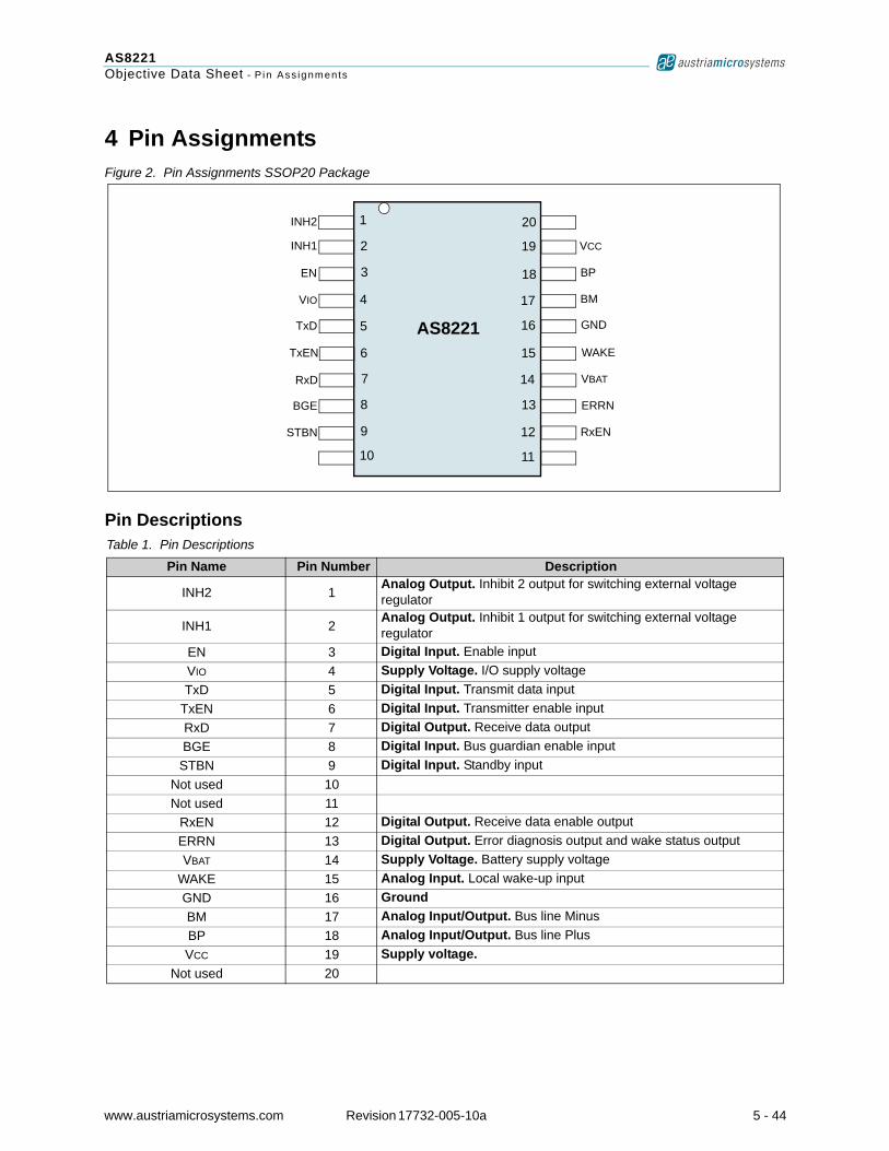
4 Pin AssignmentsFigure 2. Pin Assignments SSOP20 Package
Pin DescriptionsTable 1. Pin Descriptions
Pin Name Pin Number Description
INH2 1Analog Output. Inhibit 2 output for switching external voltage regulator
INH1 2Analog Output. Inhibit 1 output for switching external voltage regulator
EN 3 Digital Input. Enable inputVIO 4 Supply Voltage. I/O supply voltageTxD 5 Digital Input. Transmit data input
TxEN 6 Digital Input. Transmitter enable inputRxD 7 Digital Output. Receive data outputBGE 8 Digital Input. Bus guardian enable inputSTBN 9 Digital Input. Standby input
Not used 10Not used 11
RxEN 12 Digital Output. Receive data enable outputERRN 13 Digital Output. Error diagnosis output and wake status outputVBAT 14 Supply Voltage. Battery supply voltage
WAKE 15 Analog Input. Local wake-up inputGND 16 GroundBM 17 Analog Input/Output. Bus line MinusBP 18 Analog Input/Output. Bus line PlusVCC 19 Supply voltage.
Not used 20
AS8221
1
2
3
4
5
6
7
8
16
20
19
18
17
INH1
EN
VIO
TxD
TxEN
RxD
BGE
STBN
VCC
BP
BM
GND
WAKE
VBAT
ERRN
RxEN
15
14
13
9
10 11
12
INH2
www.austriamicrosystems.com Revision 17732-005-10a 5 - 44
AS8221Objective Data Sheet - Abso lu te Max imum Rat ings
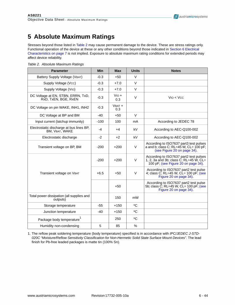
5 Absolute Maximum RatingsStresses beyond those listed in Table 2 may cause permanent damage to the device. These are stress ratings only. Functional operation of the device at these or any other conditions beyond those indicated in Section 6 Electrical Characteristics on page 7 is not implied. Exposure to absolute maximum rating conditions for extended periods may affect device reliability.
Table 2. Absolute Maximum Ratings
Parameter Min Max Units Notes
Battery Supply Voltage (VBAT) -0.3 +50 V
Supply Voltage (VCC) -0.3 +7.0 V
Supply Voltage (VIO) -0.3 +7.0 V
DC Voltage at EN, STBN, ERRN, TxD, RxD, TxEN, BGE, RxEN -0.3 VIO +
0.3 V VIO < VCC
DC Voltage on pin WAKE, INH1, INH2 -0.3 VBAT + 0.3
DC Voltage at BP and BM -40 +50 V
Input current (latchup immunity) -100 100 mA According to JEDEC 78
Electrostatic discharge at bus lines BP, BM, VBAT, WAKE -4 +4 kV According to AEC-Q100-002
Electrostatic discharge -2 +2 kV According to AEC-Q100-002
Transient voltage on BP, BM -200 +200 VAccording to ISO7637 part3 test pulses a and b; class C; RL=45 W, CL= 100 pF;
(see Figure 20 on page 34).
Transient voltage on VBAT
-200 +200 VAccording to ISO7637 part2 test pulses 1, 2, 3a and 3b; class C; RL=45 W, CL=
100 pF; (see Figure 20 on page 34).
+6.5 +50 VAccording to ISO7637 part2 test pulse 4; class C; RL=45 W, CL= 100 pF; (see
Figure 20 on page 34).
+50According to ISO7637 part2 test pulse
5b; class C; RL=45 W, CL= 100 pF; (see Figure 20 on page 34).
Total power dissipation (all supplies and outputs) 150 mW
Storage temperature -55 +150 ºC
Junction temperature -40 +150 ºC
Package body temperature1
1. The reflow peak soldering temperature (body temperature) specified is in accordance with IPC/JEDEC J-STD-020C “Moisture/Reflow Sensitivity Classification for Non-Hermetic Solid State Surface Mount Devices”. The lead finish for Pb-free leaded packages is matte tin (100% Sn).
250 ºC
Humidity non-condensing 5 85 %
www.austriamicrosystems.com Revision 17732-005-10a 6 - 44
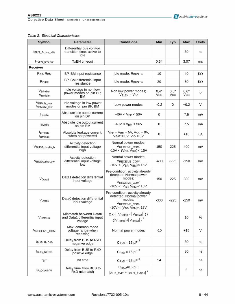
AS8221Objective Data Sheet - E lec t r i ca l Charac te r i s t i cs
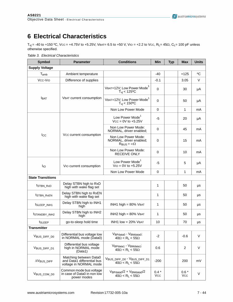
6 Electrical CharacteristicsTvj = -40 to +150 ºC, VCC = +4.75V to +5.25V, VBAT= 6.5 to +50 V, VIO = +2.2 to VCC, RL= 45Ω, CL= 100 pF unless otherwise specified.
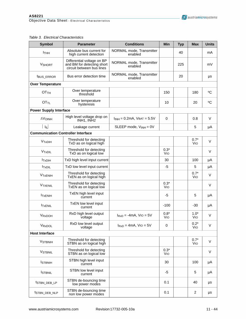
Table 3. Electrical Characteristics
Symbol Parameter Conditions Min Typ Max Units Supply Voltage
Tamb Ambient temperature -40 +125 ºC
VCC-VIO Difference of supplies -0.1 3.05 V
IBAT VBAT current consumption
VBAT=12V; Low Power Mode1 Tvj < 125ºC
0 30 µA
VBAT=12V; Low Power Mode1 Tvj < 150ºC
0 50 µA
Non Low Power Mode 0 1 mA
ICC VCC current consumption
Low Power Mode1
VCC = 0V to +5.25V-5 20 µA
Non Low Power Mode: NORMAL, driver enabled; 0 45 mA
Non Low Power Mode: NORMAL, driver enabled;
RBUS = ∞Ω0 15 mA
Non Low Power Mode: RECEIVE ONLY 0 10 mA
IIO VIO current consumption Low Power Mode1
VIO = 0V to +5.25V -5 5 µA
Non Low Power Mode 0 1 mA
State Transitions
tSTBN_RxDDelay STBN high to RxD high with wake flag set 1 50 µs
tSTBN_RxENDelay STBN high to RxEN
high with wake flag set 1 50 µs
tSLEEP_INH1Delay STBN high to INH1
high INH1 high = 80% VBAT 1 50 µs
tSTANDBY_INH2Delay STBN high to INH2
high INH2 high = 80% VBAT 1 50 µs
tSLEEP go-to-sleep hold time INH1 low = 20% VBAT 10 70 µs
Transmitter
VBUS_DIFF_D0Differential bus voltage low in NORMAL mode (Data0)
VBPdata0 - VBMdata0; 40Ω < RL < 55Ω -2 -0.6 V
VBUS_DIFF_D1Differential bus voltage high in NORMAL mode
(Data1)VBPdata1 - VBMdata1;
40Ω < RL < 55Ω 0.6 2 V
ΔVBUS_DIFFMatching between Data0 and Data1 differential bus voltage in NORMAL mode
VBUS_DIFF_D0 - VBUS_DIFF_D140Ω < RL < 55Ω -200 200 mV
VBUS_COM_D0Common mode bus voltage in case of Data0 in non low
power modesVBPdata0/2 + VBMdata0/2
40Ω < RL < 55Ω0.4 * VCC
0.6 * VCC V
www.austriamicrosystems.com Revision 17732-005-10a 7 - 44
AS8221Objective Data Sheet - E lec t r i ca l Charac te r i s t i cs
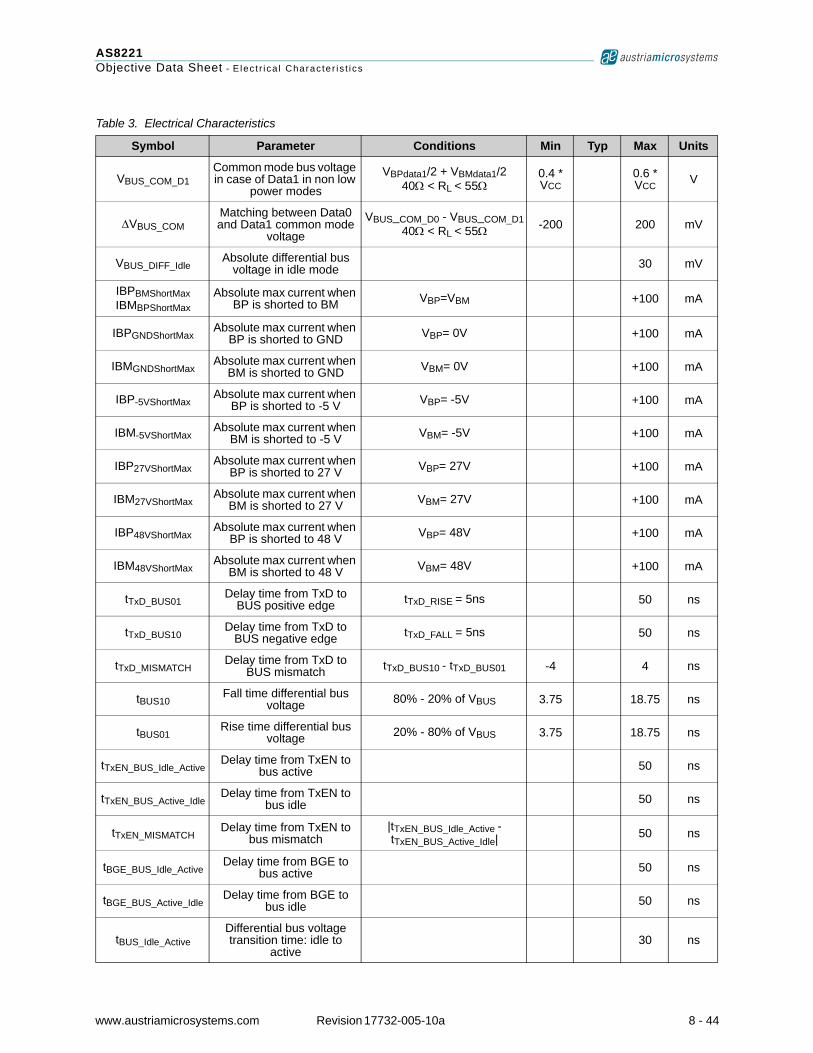
VBUS_COM_D1Common mode bus voltage in case of Data1 in non low
power modesVBPdata1/2 + VBMdata1/2
40Ω < RL < 55Ω0.4 * VCC
0.6 * VCC V
ΔVBUS_COMMatching between Data0 and Data1 common mode
voltageVBUS_COM_D0 - VBUS_COM_D1
40Ω < RL < 55Ω -200 200 mV
VBUS_DIFF_IdleAbsolute differential bus
voltage in idle mode 30 mV
IBPBMShortMaxIBMBPShortMax
Absolute max current when BP is shorted to BM VBP=VBM +100 mA
IBPGNDShortMaxAbsolute max current when
BP is shorted to GND VBP= 0V +100 mA
IBMGNDShortMaxAbsolute max current when
BM is shorted to GND VBM= 0V +100 mA
IBP-5VShortMaxAbsolute max current when
BP is shorted to -5 V VBP= -5V +100 mA
IBM-5VShortMaxAbsolute max current when
BM is shorted to -5 V VBM= -5V +100 mA
IBP27VShortMaxAbsolute max current when
BP is shorted to 27 V VBP= 27V +100 mA
IBM27VShortMaxAbsolute max current when
BM is shorted to 27 V VBM= 27V +100 mA
IBP48VShortMaxAbsolute max current when
BP is shorted to 48 V VBP= 48V +100 mA
IBM48VShortMaxAbsolute max current when
BM is shorted to 48 V VBM= 48V +100 mA
tTxD_BUS01Delay time from TxD to
BUS positive edge tTxD_RISE = 5ns 50 ns
tTxD_BUS10Delay time from TxD to
BUS negative edge tTxD_FALL = 5ns 50 ns
tTxD_MISMATCHDelay time from TxD to
BUS mismatch tTxD_BUS10 - tTxD_BUS01 -4 4 ns
tBUS10Fall time differential bus
voltage 80% - 20% of VBUS 3.75 18.75 ns
tBUS01Rise time differential bus
voltage 20% - 80% of VBUS 3.75 18.75 ns
tTxEN_BUS_Idle_ActiveDelay time from TxEN to
bus active 50 ns
tTxEN_BUS_Active_IdleDelay time from TxEN to
bus idle 50 ns
tTxEN_MISMATCHDelay time from TxEN to
bus mismatch|tTxEN_BUS_Idle_Active - tTxEN_BUS_Active_Idle| 50 ns
tBGE_BUS_Idle_ActiveDelay time from BGE to
bus active 50 ns
tBGE_BUS_Active_IdleDelay time from BGE to
bus idle 50 ns
tBUS_Idle_ActiveDifferential bus voltage transition time: idle to
active30 ns
Table 3. Electrical Characteristics
Symbol Parameter Conditions Min Typ Max Units
www.austriamicrosystems.com Revision 17732-005-10a 8 - 44
AS8221Objective Data Sheet - E lec t r i ca l Charac te r i s t i cs
tBUS_Active_IdleDifferential bus voltage transition time: active to
idle30 ns
tTxEN_timeout TxEN timeout 0.64 3.07 ms
Receiver
RBP, RBM BP, BM input resistance Idle mode; RBUS=∞ 10 40 KΩ
RDIFFBP, BM differential input
resistance Idle mode; RBUS=∞ 20 80 KΩ
VBPidle,VBMidle
Idle voltage in non low power modes on pin BP,
BMNon low power modes;
VTxEN = VIO0.4* VCC
0.5* VCC
0.6* VCC V
VBPidle_low, VBMidle_low
Idle voltage in low power modes on pin BP, BM Low power modes -0.2 0 +0.2 V
IBPidleAbsolute idle output current
on pin BP -40V < VBP < 50V 0 7.5 mA
IBMidleAbsolute idle output current
on pin BM -40V < VBM < 50V 0 7.5 mA
IBPleak,IBMleak
Absolute leakage current, when not powered
VBP = VBM = 5V, VCC = 0V, VBAT = 0V; VIO = 0V 0 +10 uA
VBUSActiveHighActivity detection
differential input voltage high
Normal power modes;VRECEIVE_COM:
-10V < (VBP, VBM) < 15V150 225 400 mV
VBUSActiveLowActivity detection
differential input voltage low
Normal power modes;VRECEIVE_COM:
-10V < (VBP, VBM)< 15V-400 -225 -150 mV
VData1Data1 detection differential
input voltage
Pre-condition: activity already detected. Normal power
modes;VRECEIVE_COM:
-10V < (VBP, VBM)< 15V
150 225 300 mV
VData0Data0 detection differential
input voltage
Pre-condition: activity already detected. Normal power
modes;VRECEIVE_COM:
-10V < (VBP, VBM)< 15V
-300 -225 -150 mV
VDataErrMismatch between Data0
and Data1 differential input voltage
2 x (⎜⎜VData0⎜- ⎜VData1⎜⎜) /
(⎜VData0⎜+⎜VData1⎜) 210 %
VRECEIVE_COMMax. common mode voltage range when
receivingNormal power modes -10 +15 V
tBUS_RxD10Delay from BUS to RxD
negative edge CRxD = 15 pF 3 80 ns
tBUS_RxD01Delay from BUS to RxD
positive edge CRxD = 15 pF 3 80 ns
tBIT Bit time CRxD = 15 pF 3 54 ns
tRxD_ASYMDelay time from BUS to
RxD mismatchCRXD=15 pF;
|tBUS_RxD10- tBUS_RxD01| 35 ns
Table 3. Electrical Characteristics
Symbol Parameter Conditions Min Typ Max Units
www.austriamicrosystems.com Revision 17732-005-10a 9 - 44
AS8221Objective Data Sheet - E lec t r i ca l Charac te r i s t i cs
tRxD_FALL Fall time RxD voltage80% - 20% of VRxD;
CRxD=15 pF 35 ns
tRxD_RISE Rise time RxD voltage20% - 80% of VRxD;
CRxD=15 pF 35 ns
tBUSIdleDetection Idle detection time VBUS: 400mV → 0V 50 200 ns
tBUSActivitiyDetection Activity detection time VBUS: 0V → 400mV 100 250 ns
tBUSIdleReaction Idle reaction time VBUS: 400mV → 0V 50 300 ns
tBUSActivityReaction Activity reaction time VBUS: 0V → 400mV 100 350 ns
Wake-Up Detector
tBWU_D0Data0 detection time in remote wake-up pattern -10V < (VBP, VBM) < 15V 1 4 µs
tBWU_IdleIdle or Data1 detection time in remote wake-up pattern -10V < (VBP, VBM) < 15V 1 4 µs
tBWU_DetectTotal remote wake-up
detection time -10V < (VBP, VBM) < 15V 48 140 µs
VBWUTHBus wake-up detection
threshold -10V < (VBP, VBM) < 15V -300 -150 mV
VLWUTHLocal wake-up detection
threshold -2 4 V
ILWULLow level input current on
local WAKE pinVBAT = 12V; VLWAKE = 2V for t
< tLWUFilter-20 -5 µA
ILWUHHigh level input current on
local WAKE pinVBAT = 12V; VLWAKE = 4V for t
< tLWUFilter5 20 µA
tLWUFilter Local wake filter time 1 40 µs
Supply Voltage Monitor
VBATTHHVBAT undervoltage recovery threshold 3.5 4.5 V
VBATTHLVBAT undervoltage detection threshold 2.5 3.5 V
VCCTHHVCC under-voltage recovery threshold 3.5 4.5 V
VCCTHLVCC undervoltage detection
threshold 2.5 3.5 V
VIOTHHVIO undervoltage recovery
threshold 1.25 2.0 V
VIOTHLVIO undervoltage detection
threshold 0.75 1.5 V
tUV_DETECTDetection time for
undervoltage at VBAT, VCC, VIO
100 700 ms
tUV_REC Detection time for
undervoltage recovery at VBAT, VCC, VIO
0.7 5 ms
Bus Error Detection
ITHLAbsolute bus current for
low current detectionNORMAL mode, Transmitter
enabled 5 mA
Table 3. Electrical Characteristics
Symbol Parameter Conditions Min Typ Max Units
www.austriamicrosystems.com Revision 17732-005-10a 10 - 44
AS8221Objective Data Sheet - E lec t r i ca l Charac te r i s t i cs
ITHHAbsolute bus current for high current detection
NORMAL mode, Transmitter enabled 40 mA
VSHORTDifferential voltage on BP and BM for detecting short circuit between bus lines
NORMAL mode, Transmitter enabled 225 mV
tBUS_ERROR Bus error detection time NORMAL mode, Transmitter enabled 20 µs
Over Temperature
OTTHOver temperature
threshold 150 180 ºC
OTTLOver temperature
hysteresis 10 20 ºC
Power Supply Interface
ΔVOINHHigh level voltage drop on
INH1, INH2 IINH = 0.2mA, VBAT = 5.5V 0 0.8 V
⏐IIL⏐ Leakage current SLEEP mode, VINH = 0V 5 µA
Communication Controller Interface
VTxDIHThreshold for detecting TxD as on logical high
0.7* VIO V
VTxDILThreshold for detecting TxD as on logical low
0.3* VIO V
ITxDIH TxD high level input current 30 100 µA
ITxDIL TxD low level input current -5 5 µA
VTxENIHThreshold for detecting TxEN as on logical high
0.7* VIO V
VTXENILThreshold for detecting TxEN as on logical low
0.3* VIO V
ITxENIHTxEN high level input
current -5 5 µA
ITxENILTxEN low level input
current -100 -30 µA
VRxDOHRxD high level output
voltage IRxD = -4mA, VIO = 5V 0.8* VIO
1.0* VIO V
VRxDOLRxD low level output
voltage IRxD = 4mA, VIO = 5V 0 0.2* VIO V
Host Interface
VSTBNIHThreshold for detecting STBN as on logical high
0.7* VIO V
VSTBNILThreshold for detecting STBN as on logical low
0.3* VIO V
ISTBNIHSTBN high level input
current 30 100 µA
ISTBNILSTBN low level input
current -5 5 µA
tSTBN_DEB_LPSTBN de-bouncing time
low power modes 0.1 40 µs
tSTBN_DEB_NLPSTBN de-bouncing time non low power modes 0.1 2 µs
Table 3. Electrical Characteristics
Symbol Parameter Conditions Min Typ Max Units
www.austriamicrosystems.com Revision 17732-005-10a 11 - 44
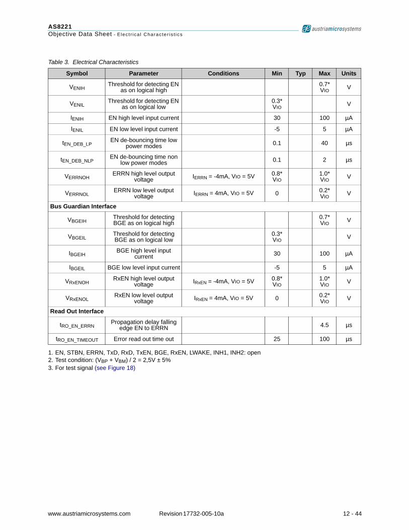
AS8221Objective Data Sheet - E lec t r i ca l Charac te r i s t i cs
VENIHThreshold for detecting EN
as on logical high 0.7* VIO V
VENILThreshold for detecting EN
as on logical low0.3* VIO V
IENIH EN high level input current 30 100 µA
IENIL EN low level input current -5 5 µA
tEN_DEB_LPEN de-bouncing time low
power modes 0.1 40 µs
tEN_DEB_NLPEN de-bouncing time non
low power modes 0.1 2 µs
VERRNOHERRN high level output
voltage IERRN = -4mA, VIO = 5V 0.8* VIO
1.0* VIO V
VERRNOLERRN low level output
voltage IERRN = 4mA, VIO = 5V 0 0.2* VIO V
Bus Guardian Interface
VBGEIHThreshold for detecting BGE as on logical high
0.7* VIO V
VBGEILThreshold for detecting BGE as on logical low
0.3* VIO V
IBGEIHBGE high level input
current 30 100 µA
IBGEIL BGE low level input current -5 5 µA
VRxENOHRxEN high level output
voltage IRxEN = -4mA, VIO = 5V 0.8* VIO
1.0* VIO V
VRxENOLRxEN low level output
voltage IRxEN = 4mA, VIO = 5V 0 0.2* VIO V
Read Out Interface
tRO_EN_ERRNPropagation delay falling
edge EN to ERRN 4.5 µs
tRO_EN_TIMEOUT Error read out time out 25 100 µs
1. EN, STBN, ERRN, TxD, RxD, TxEN, BGE, RxEN, LWAKE, INH1, INH2: open2. Test condition: (VBP + VBM) / 2 = 2,5V ± 5%3. For test signal (see Figure 18)
Table 3. Electrical Characteristics
Symbol Parameter Conditions Min Typ Max Units
www.austriamicrosystems.com Revision 17732-005-10a 12 - 44
AS8221Objective Data Sheet - Typ ica l Opera t ing Charac te r i s t i cs
7 Typical Operating CharacteristicsFigure 3. Figure 4.
Figure 5. Figure 6.
Figure 7. Figure 8.
www.austriamicrosystems.com Revision 17732-005-10a 13 - 44
AS8221Objective Data Sheet - De ta i led Descr ip t ion
8 Detailed DescriptionThe AS8221 is a high-speed fault tolerant device operating as an interface between a generic controller and the copper wire physical bus. The AS8221 is designed to extend the application range for high speed and safety critical time triggered bus systems in an automotive environment. The drivers are short circuit protected against the positive and negative supply voltage to increase the robustness and reliability of automotive systems. The AS8221 operates at baudrates up to 10 Mbps to increase the bandwidth for automotive applications.
Block DescriptionThe electrical AS8221 high-speed bus-system transceiver is the interface between a FlexRay™ network node module and the channel. The transceiver provides differential transmit and receive capability to the bus, allowing the node module bidirectional time multiplexed binary data stream transfer. Besides the transmit and receive function, the transceiver provides low power management, supply voltage monitoring (under voltage detection) as well as bus failure detection and represents a ESD-protection barrier between the bus and the ECU.
The AS8221 consists of 9 different functional blocks(see Figure 1):
EventsTransitions in order to change between the operation modes are possible only when events are detected. The device supports three type of events, events on the host controller interface (STBN, EN), detection of undervoltage or supply voltage recovery, and detected wake events. Whenever an event is recognized, a transition can be performed.
Operating ModesThe AS8221 provides the following operating modes: NORMAL: non low power mode RECEIVE ONLY: non low power mode
Table 4. Functional Blocks
Functional Block Short Description
Host Controller Interface (HCI)Digital interface between the transceiver and the host controller (HC)The host interface comprises the read out handler, which delivers failure and status information via the ERRN pin to the host controller.
Communication Controller Interface (CCI)
Digital interface between the transceiver and the FlexRay communication controller (CC)
Bus Guarding Interface (BGI) Digital interface between the transceiver and the FlexRay bus guardian (BG)
Power Supply Interface(PSI)
The power supply interface consists of an sub functional block, the voltage monitor (VM) and includes two analogue inhibit outputs for signalling the internal state of the transceiver
Internal Logic (IL)
The digital signals from the functional blocks of the device are fed into the internal logic where the forwarding of FlexRay messages from analogue side to digital interfaces and vice versa is done. The state machine is performed in this block and is dealing the error, wake and power-on flags.
Bus Failure Detector (BFD)Temperature Protection (TP)
The bus failure detector is directly connected to the bus pins, in order to detect several external failure conditions which may occur on the bus.The temperature protection turns off the output driver when reaching the specified internal temperature in order to protect the device.
Transmitter The transmitter provides the bus signals as specified on the bus lines.
ReceiverThe receiver captures FlexRay valid signals on the bus lines and provides received data streams to the internal logic
Wake-Up Detector (WUD)The wake-up detector recognizes valid wake-up frames on the bus, recognizes a wake signal on the local WAKE pin and signals valid wake-up events to the internal logic.
www.austriamicrosystems.com Revision 17732-005-10a 14 - 44
AS8221Objective Data Sheet - De ta i led Descr ip t ion
STANDBY: low power mode GO TO SLEEP: low power mode SLEEP: low power mode
NORMAL modeIn this mode the transceiver is able to send and receive data signals on the bus. TxEN and BGE control the state of the transmitter. INH1 and INH2 outputs are set high. RxD reflects the bus data and reflect the bus state. The error read out mechanism is enabled. In this mode, the transmitter state can be selected as shown in the Table 5. In case the over-temperature flag is set the transmitter is disabled. The bus wires are terminated to VCC/2 via receiver input resistances.
If the differential bus voltage is higher than VBUSActivehigh or lower than VBUSActivelow for a time longer than tBUSAc-tivityDetection, then activity is detected on the bus (Bus = active), RxEN is switched to logical “low” and RxD is released. If, after the activity detection, the differential bus voltage is higher than VData1, RxD is high.
If, after the activity detection, the differential bus voltage is lover than VData0, RxD is low.
If the absolute differential bus voltage is lower than VBUSActivehigh and higher than VBUSActivelow for a time longer than tBUSIdleDetection, then idle is detected on the bus (Bus = idle), RxEN and RxD are switched to logical “high”
RECEIVE ONLY modeIn this mode the transceiver has the same behaviour as in NORMAL mode but the transmitter is disabled.
STANDBY modeIn this mode the transceiver is not able to send and receive data signals from the bus, but the wake-up detector is active. The power consumption is significantly reduced respect the non low power operation modes. RxD and RxEN, reflects the negation of the wake-up flag. INH1 is set to high. If wake-up flag is set then INH2 is high, otherwise it is floating. The error read out mechanism is not enabled. The bus wires are terminated to GND (bus state: Idle_LP).
GO TO SLEEP modeIn this mode the transceiver has the same behavior as in STANDBY mode but if this mode is selected for a time longer than tSLEEP and the wake flag is cleared the device enters into the SLEEP mode.
SLEEP modeIn this mode the transceiver has the same behaviour as in STANDBY mode but INH1 and INH2 are floating.
Non Operating ModeThe AS8221 provides the following non operating mode:
POWER OFFIn this mode the transceiver is not able to operate. RxD, RxEN are set to high and ERRN is set to low. INH1 and INH2 are floating. The bus wires are not connected to GND (bus state: Idle_HZ).
Table 5. Transmitter State
BGE TxEN TxD Transmitter state Bus State
H L H Enabled Data1 (BP is driven high, BM is driven low)
H L L Enabled Data0 (BP is driven low, BM is driven High)
X H X Disabled Idle (BP and BM are not driven)
L X X Disabled Idle (BP and BM are not driven)
www.austriamicrosystems.com Revision 17732-005-10a 15 - 44
AS8221Objective Data Sheet - De ta i led Descr ip t ion
Undervoltage Events
Undervoltage VBAT
When VBAT voltage falls below VBATTHL for a time longer than tUV_DETECT then the undervoltage VBAT flag is set and it is reset when VBAT exceeds the voltage threshold VBATTHH for a time longer than tUV_REC or in case a wake-up event has been detected. The flag can be set or reset in all the modes.
Undervoltage VIO
When VIO voltage falls below VIOTHL for a time longer than tUV_DETECT then the undervoltage VIO flag is set and it is reset when VIO exceeds the voltage threshold VIOTHH for a time longer than tUV_REC or in case a wake-up event has been detected. The flag can be set or reset in all the operation modes. The flag is reset at POWER OFF.
Undervoltage VCC
When VCC voltage falls below VCCTHL for a time longer than tUV_DETECT then the undervoltage VCC flag is set and it is reset when VCC exceeds the voltage threshold VCCTHH for a time longer than tUV_REC or in case a wake-up event has been detected. The flag can be set or reset in all the operation modes. The flag is reset at POWER OFF.
Power On/Off Events Starting from POWER OFF mode a power on event occurs in case VBAT undervoltage flag is reset. Starting from every operation mode a power off event occurs in case VBAT and VCC undervoltage flags are set.
Wake-Up EventsA wake-up event can be detected only in low power modes. The wake-up flag is set when the remote or local wake flag is set. The wake-up flag is reset when the remote and local wake-up flags are reset. The remote wake-up flag is set if a remote wake-up event occurs. The local wake-up flag is set if a local wake-up event occurs. The remote and local wake-up flags are reset entering a low power mode from a non low power mode, entering NORMAL mode, whenever an undervoltage event occurs and at POWER OFF.
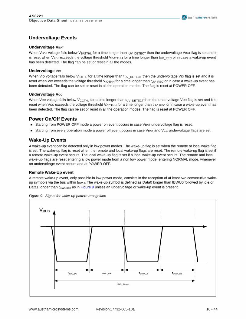
Remote Wake-Up eventA remote wake-up event, only possible in low power mode, consists in the reception of at least two consecutive wake-up symbols via the bus within tBWU. The wake-up symbol is defined as Data0 longer than tBWU0 followed by idle or Data1 longer than tBWUidle as in Figure 9 unless an undervoltage or wake-up event is present.
Figure 9. Signal for wake-up pattern recognition
tBWU_D0 tBWU_Idle
tBWU_Detect
VBUS
tBWU_D0 tBWU_Idle
www.austriamicrosystems.com Revision 17732-005-10a 16 - 44
AS8221Objective Data Sheet - De ta i led Descr ip t ion
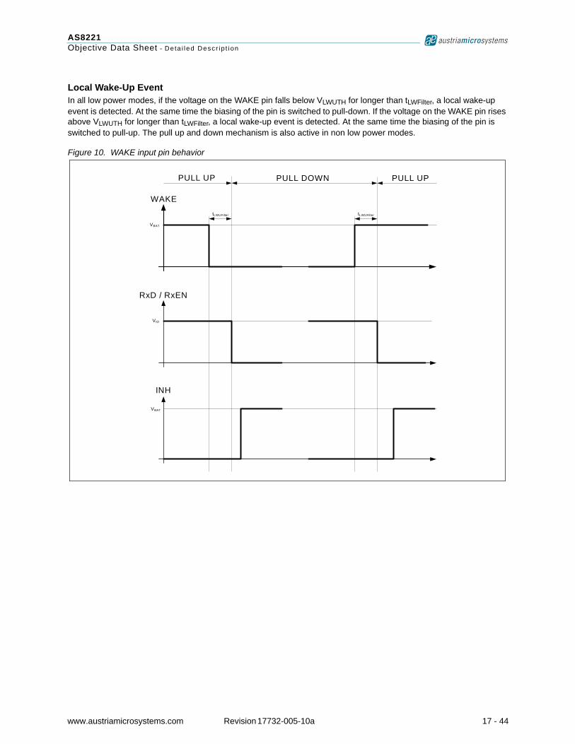
Local Wake-Up EventIn all low power modes, if the voltage on the WAKE pin falls below VLWUTH for longer than tLWFilter, a local wake-up event is detected. At the same time the biasing of the pin is switched to pull-down. If the voltage on the WAKE pin rises above VLWUTH for longer than tLWFilter, a local wake-up event is detected. At the same time the biasing of the pin is switched to pull-up. The pull up and down mechanism is also active in non low power modes.
Figure 10. WAKE input pin behavior
WAKE
RxD / RxEN
INH
tLWUFilter
PULL UP PULL UPPULL DOWN
VBAT
VBAT
VIO
tLWUFilter
www.austriamicrosystems.com Revision 17732-005-10a 17 - 44
AS8221Objective Data Sheet - De ta i led Descr ip t ion
System Description
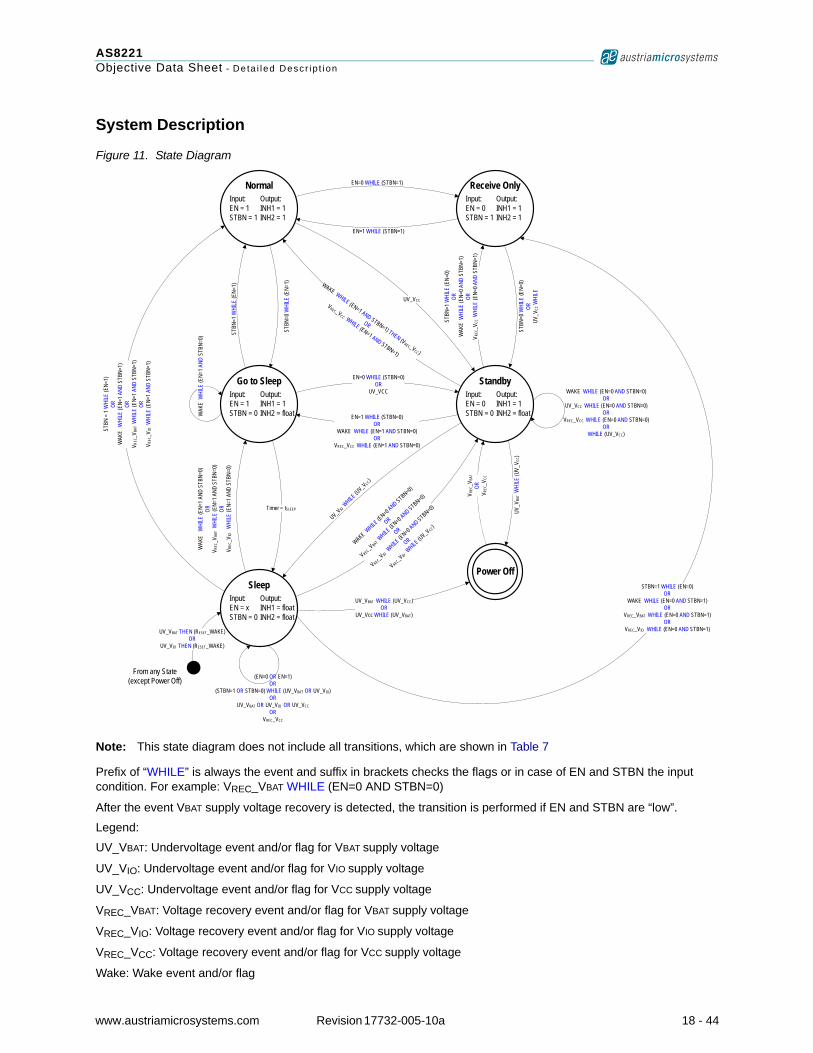
Figure 11. State Diagram
Note: This state diagram does not include all transitions, which are shown in Table 7
Prefix of “WHILE” is always the event and suffix in brackets checks the flags or in case of EN and STBN the input condition. For example: VREC_VBAT WHILE (EN=0 AND STBN=0)
After the event VBAT supply voltage recovery is detected, the transition is performed if EN and STBN are “low”.
Legend:
UV_VBAT: Undervoltage event and/or flag for VBAT supply voltage
UV_VIO: Undervoltage event and/or flag for VIO supply voltage
UV_VCC: Undervoltage event and/or flag for VCC supply voltage
VREC_VBAT: Voltage recovery event and/or flag for VBAT supply voltage
VREC_VIO: Voltage recovery event and/or flag for VIO supply voltage
VREC_VCC: Voltage recovery event and/or flag for VCC supply voltage
Wake: Wake event and/or flag
UV_VIO WHILE
(UV_VCC)
Power Off
Normal Receive Only
Go to Sleep Standby
Sleep
EN=0 WHILE (STBN=1)
EN=1 WHILE (STBN=1)
STBN
=0W
HILE
(EN=
0)OR
UV_V
CCW
HILE
STBN
=1 W
HILE
(EN=
0)OR
WAK
E W
HILE
(EN=
0AND
STB
N=1)
ORV R
EC_V
CC W
HILE
(EN=
0AND
STB
N=1)
WAKE WHILE (EN=1 AND STBN=1) THEN (VREC_VCC)
OR
VREC_VCC WHILE (EN=1 AND STBN=1)
UV_VCC
STBN
=0W
HILE
(EN=
1)
STBN
=1W
HILE
(EN=
1)
UV_VBAT THEN (RESET_WAKE)OR
UV_VIO THEN (RESET_WAKE)
From any State(except Power Off)
EN=0 WHILE (STBN=0)OR
UV_VCC
EN=1 WHILE (STBN=0)OR
WAKE WHILE (EN=1 AND STBN=0)OR
VREC_VCC WHILE (EN=1 AND STBN=0)
Timer = tSLEEP
WAK
E W
HILE
(EN=
1 AND
STB
N=0)
ORV R
EC_V
BAT
WHI
LE(E
N=1 A
ND S
TBN=
0)OR
V REC
_VIO
WHI
LE(E
N=1 A
ND S
TBN=
0)
STBN
= 1
WHI
LE(E
N=1)
ORW
AKE
WHI
LE(E
N=1A
ND S
TBN=
1)OR
V REC
_VBA
T W
HILE
(EN=
1AND
STB
N=1)
ORV R
EC_V
IO
WHI
LE(E
N=1A
ND S
TBN=
1)
WAKE WHILE
(EN=0AND STBN=0)
OR
VREC_VBAT W
HILE(EN=0
AND STBN=0)
OR
VREC_VIO W
HILE(EN=0
AND STBN=0)
OR
VREC_VIO W
HILE(UV_VCC)
STBN=1 WHILE (EN=0)OR
WAKE WHILE (EN=0 AND STBN=1) OR
VREC_VBAT WHILE (EN=0 AND STBN=1)OR
VREC_VIO WHILE (EN=0 AND STBN=1)
Input:EN = 1STBN = 1
Output:INH1 = 1INH2 = 1
Input:EN = 1STBN = 0
Output:INH1 = 1INH2 = float
Input:EN = 0STBN = 1
Output:INH1 = 1INH2 = 1
Input:EN = 0STBN = 0
Output:INH1 = 1INH2 = float
Input:EN = xSTBN = 0
Output:INH1 = floatINH2 = float
UV_VBAT WHILE (UV_VCC)OR
UV_Vcc WHILE (UV_VBAT)
UV_V
BAT
WHI
LE (U
V_V C
C)
V REC
_VBA
TOR
V REC
_VCC
WAKE WHILE (EN=0 AND STBN=0)OR
UV_VCC WHILE (EN=0 AND STBN=0)OR
VREC_VCC WHILE (EN=0 AND STBN=0)OR
WHILE (UV_VCC)
WAK
E W
HILE
(EN=
1AND
STB
N=0)
(EN=0 OR EN=1)OR
(STBN=1 OR STBN=0) WHILE (UV_VBAT OR UV_VIO)OR
UV_VBAT OR UV_VIO OR UV_VCCOR
VREC_VCC
www.austriamicrosystems.com Revision 17732-005-10a 18 - 44
AS8221Objective Data Sheet - De ta i led Descr ip t ion
Fail Silent BehaviorIn order to be fail silent, undervoltage detection on the three power supplies VBAT, VIO and VCC is implemented VBAT: Battery supply voltage
VIO: Supply voltage for I/O digital level adaptation
VCC: Supply voltage (+5V)
State transitions due to under voltage detection In case of VBAT or VIO undervoltage is detected, SLEEP mode will be entered regardless of the voltage present on
pins EN and STBN. In case VCC undervoltage is detected, STANDBY mode will be entered regardless of the voltage present on pins
EN and STBN. VBAT and VIO undervoltage detection have higher priority than VCC undervoltage detection. In case VBAT and VCC undervoltage are detected, POWER OFF mode is entered (bus state: Idle_HZ).
State transitions due to voltage recovery detection If the undervoltage recovers the device will enter the mode determined by the voltages at pins EN and STBN. Starting from the Power Off, the device enters the state indicated by the host input pins (EN, STBN) only when
VBAT or VCC recovers (VBAT ≥ VBATTHH or VCC ≥ VCCTHH) while VIO is available (undervoltage flag of VIO flag not set). If the VIO undervoltage flag is set, the STANDBY mode will be entered. In both cases the Power On flag is set. When VBAT ≤ VBATTHL and VCC ≤ VCCTHL the device is in power off state and the bus wires are not terminated (bus
state: Idle_HZ).
Wake-Up MechanismThe wake-up detector is active in all low power modes. In case a remote o local wake-up occurs the VBAT, VIO, VCC undervoltage flags are reset, the wake-up flag is set, INH outputs are switched on and the device enters the state indicated by the host pins.
Remote Wake-UpA remote wake-up event or bus wake-up event is the reception of at least two consecutive wake-up symbols via the bus within tBWU. The wake-up symbol is defined as Data0 longer than tBWU0 followed by idle or Data1 longer than tBWUIdle.
Mode TransitionsStarting from every operation mode the device enters POWER OFF in case a power off event occurs regardless the VIO undervoltage flag, the wake-up flag and the host input pins (EN, STBN) state.
Starting from the POWER OFF the device enters STANDBY only in case a power on event occurs.
Starting from every operation mode the device enters SLEEP in case VBAT or VIO undervoltage flag is set regardless the VCC undervoltage flag, the wake-up flag and the host input pins state.
Starting from every operation mode except SLEEP the device enters STANDBY in case VCC undervoltage flag is set and VBAT and VIO undervoltage flags are not set, regardless the wake-up flag indication and the host input pins state.
Starting from a low power mode the device enters the operation mode indicated by the host input pins if a wake-up event occurs.
In case all the undervoltage flags are reset the operation mode is selected by the wake-up flag and the host pins according to Table 6.
www.austriamicrosystems.com Revision 17732-005-10a 19 - 44
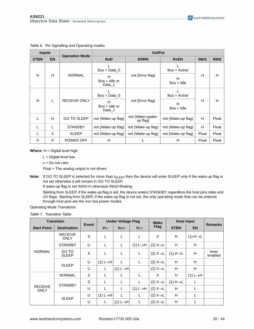
AS8221Objective Data Sheet - De ta i led Descr ip t ion
Where: H = Digital level high
L = Digital level lowx = Do not careFloat = The analog output is not driven
Note: If GO TO SLEEP is selected for more than tSLEEP then the device will enter SLEEP only if the wake-up flag is not set otherwise it will remain in GO TO SLEEP. If wake-up flag is set INH2=H otherwise INH2=floating.Starting from SLEEP, if the wake-up flag is set, the device enters STANDBY regardless the host pins state and UV flags. Starting from SLEEP, if the wake-up flag is not set, the only operating mode that can be entered through host pins are the non low power modes.
Operating Mode Transitions
Table 6. Pin Signalling and Operating modes
InputsOperation Mode
OutPut
STBN EN RxD ERRN RxEN INH1 INH2
H H NORMAL
LBus = Data_0
not (Error flag)
LBus = Active
H HHBus = Idle or
Data_1H
Bus = Idle
H L RECEIVE ONLY
LBus = Data_0
not (Error flag)
LBus = Active
H HHBus = Idle or
Data_1H
Bus = Idle
L H GO TO SLEEP not (Wake-up flag) not (Wake-upake-up flag) not (Wake-up flag) H Float
L L STANDBY not (Wake-up flag) not (Wake-up flag) not (Wake-up flag) H Float
L X SLEEP not (Wake-up flag) not (Wake-up flag) not (Wake-up flag) Float Float
X X POWER OFF H L H Float Float
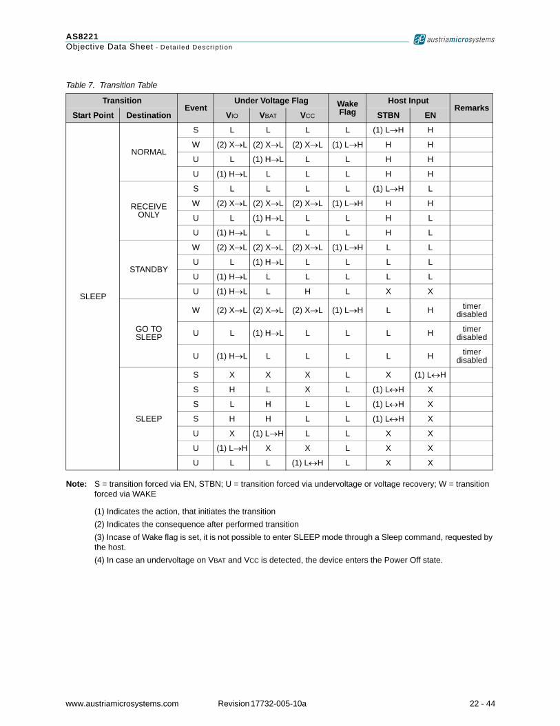
Table 7. Transition Table
TransitionEvent
Under Voltage Flag Wake Flag
Host InputRemarks
Start Point Destination VIO VBAT VCC STBN EN
NORMAL
RECEIVE ONLY S L L L X H (1) H→L
STANDBY U L L (1) L→H (2) X→L H H
GO TO SLEEP S L L L (2) X→L (1) H→L H timer
enabled
SLEEPU (1) L→H L L (2) X→L H H
U L (1) L→H (2) X→L H H
RECEIVE ONLY
NORMAL S L L L X H (1) L→H
STANDBYS L L L (2) X→L (1) H→L L
U L L (1) L→H (2) X→L H L
SLEEPU (1) L→H L L (2) X→L H L
U L (1) L→H L (2) X→L H L
www.austriamicrosystems.com Revision 17732-005-10a 20 - 44
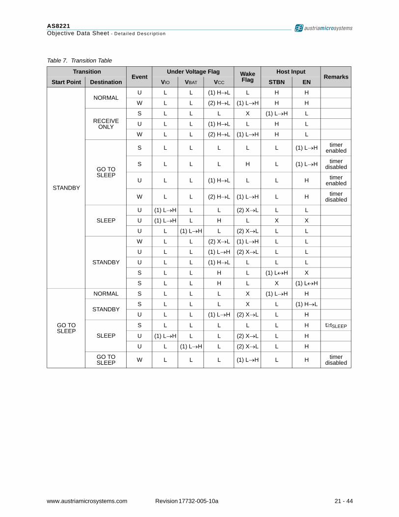
AS8221Objective Data Sheet - De ta i led Descr ip t ion
STANDBY
NORMALU L L (1) H→L L H H
W L L (2) H→L (1) L→H H H
RECEIVE ONLY
S L L L X (1) L→H L
U L L (1) H→L L H L
W L L (2) H→L (1) L→H H L
GO TO SLEEP
S L L L L L (1) L→H timer enabled
S L L L H L (1) L→H timer disabled
U L L (1) H→L L L H timer enabled
W L L (2) H→L (1) L→H L H timer disabled
SLEEP
U (1) L→H L L (2) X→L L L
U (1) L→H L H L X X
U L (1) L→H L (2) X→L L L
STANDBY
W L L (2) X→L (1) L→H L L
U L L (1) L→H (2) X→L L L
U L L (1) H→L L L L
S L L H L (1) L↔H X
S L L H L X (1) L↔H
GO TO SLEEP
NORMAL S L L L X (1) L→H H
STANDBYS L L L X L (1) H→L
U L L (1) L→H (2) X→L L H
SLEEP
S L L L L L H t≥tSLEEP
U (1) L→H L L (2) X→L L H
U L (1) L→H L (2) X→L L H
GO TO SLEEP W L L L (1) L→H L H timer
disabled
Table 7. Transition Table
TransitionEvent
Under Voltage Flag Wake Flag
Host InputRemarks
Start Point Destination VIO VBAT VCC STBN EN
www.austriamicrosystems.com Revision 17732-005-10a 21 - 44
AS8221Objective Data Sheet - De ta i led Descr ip t ion
Note: S = transition forced via EN, STBN; U = transition forced via undervoltage or voltage recovery; W = transition forced via WAKE
(1) Indicates the action, that initiates the transition(2) Indicates the consequence after performed transition(3) Incase of Wake flag is set, it is not possible to enter SLEEP mode through a Sleep command, requested by the host.(4) In case an undervoltage on VBAT and VCC is detected, the device enters the Power Off state.
SLEEP
NORMAL
S L L L L (1) L→H H
W (2) X→L (2) X→L (2) X→L (1) L→H H H
U L (1) H→L L L H H
U (1) H→L L L L H H
RECEIVE ONLY
S L L L L (1) L→H L
W (2) X→L (2) X→L (2) X→L (1) L→H H H
U L (1) H→L L L H L
U (1) H→L L L L H L
STANDBY
W (2) X→L (2) X→L (2) X→L (1) L→H L L
U L (1) H→L L L L L
U (1) H→L L L L L L
U (1) H→L L H L X X
GO TO SLEEP
W (2) X→L (2) X→L (2) X→L (1) L→H L H timer disabled
U L (1) H→L L L L H timer disabled
U (1) H→L L L L L H timer disabled
SLEEP
S X X X L X (1) L↔H
S H L X L (1) L↔H X
S L H L L (1) L↔H X
S H H L L (1) L↔H X
U X (1) L→H L L X X
U (1) L→H X X L X X
U L L (1) L↔H L X X
Table 7. Transition Table
TransitionEvent
Under Voltage Flag Wake Flag
Host InputRemarks
Start Point Destination VIO VBAT VCC STBN EN
www.austriamicrosystems.com Revision 17732-005-10a 22 - 44
AS8221Objective Data Sheet - De ta i led Descr ip t ion
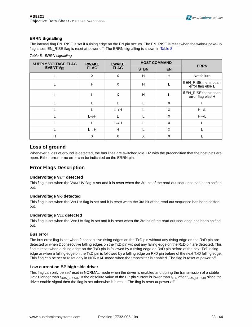
ERRN SignallingThe internal flag EN_RISE is set if a rising edge on the EN pin occurs. The EN_RISE is reset when the wake-upake-up flag is set. EN_RISE flag is reset at power off. The ERRN signalling is shown in Table 8.
Loss of groundWhenever a loss of ground is detected, the bus lines are switched Idle_HZ with the precondition that the host pins are open. Either error or no error can be indicated on the ERRN pin.
Error Flags Description
Undervoltage VBAT detectedThis flag is set when the VBAT UV flag is set and it is reset when the 3rd bit of the read out sequence has been shifted out.
Undervoltage VIO detectedThis flag is set when the VIO UV flag is set and it is reset when the 3rd bit of the read out sequence has been shifted out.
Undervoltage VCC detectedThis flag is set when the VCC UV flag is set and it is reset when the 3rd bit of the read out sequence has been shifted out.
Bus errorThe bus error flag is set when 2 consecutive rising edges on the TxD pin without any rising edge on the RxD pin are detected or when 2 consecutive falling edges on the TxD pin without any falling edge on the RxD pin are detected. This flag is reset when a rising edge on the TxD pin is followed by a rising edge on RxD pin before of the next TxD rising edge or when a falling edge on the TxD pin is followed by a falling edge on RxD pin before of the next TxD falling edge. This flag can be set or reset only in NORMAL mode when the transmitter is enabled. The flag is reset at power off.
Low current on BP high side driverThis flag can only be set/reset in NORMAL mode when the driver is enabled and during the transmission of a stable Data1 longer than tBUS_ERROR. If the absolute value of the BP pin current is lower than ITHL after tBUS_ERROR since the driver enable signal then the flag is set otherwise it is reset. The flag is reset at power off.
Table 8. ERRN signalling
SUPPLY VOLTAGE FLAG EVENT VIO
RWAKE FLAG
LWAKE FLAG
HOST COMMANDERRN
STBN EN
L X X H H Not failure
L H X H L If EN_RISE then not an error flag else L
L L X H L If EN_RISE then not an error flag else H
L L L L X H
L L L→H L X H→L
L L→H L L X H→L
L H L→H L X L
L L→H H L X L
H X X X X L
www.austriamicrosystems.com Revision 17732-005-10a 23 - 44
AS8221Objective Data Sheet - De ta i led Descr ip t ion
Low current on BP low side driverThis flag can only be set/reset in NORMAL mode when the driver is enabled and during the transmission of a stable Data0 longer than tBUS_ERROR. If the absolute value of the BP pin current is lower than ITHL after tBUS_ERROR since the driver enable signal then the flag is set otherwise it is reset. The flag is reset at power off.
Low current on BM high side driverThis flag can only be set/reset in NORMAL mode when the driver is enabled and during the transmission of a stable Data0 longer than tBUS_ERROR. If the absolute value of the BM pin current is lower than ITHL after tBUS_ERROR since the driver enable signal then the flag is set otherwise it is reset. The flag is reset at power off.
Low current on BM low side driverThis flag can only be set/reset in NORMAL mode when the driver is enabled and during the transmission of a stable Data1 longer than tBUS_ERROR. If the absolute value of the BM pin current is lower than ITHL after tBUS_ERROR since the driver enable signal then the flag is set otherwise it is reset. The flag is reset at power off.
High current on BP high side driverThis flag can only be set/reset in NORMAL mode when the driver is enabled and during the transmission of a stable Data1 longer than tBUS_ERROR. If the absolute value of the BP pin current is higher than ITHH after tBUS_ERROR since the driver enable signal then the flag is set otherwise it is reset. The flag is reset at power off.
High current on BP low side driverThis flag can only be set/reset in NORMAL mode when the driver is enabled and during the transmission of a stable Data0 longer than tBUS_ERROR. If the absolute value of the BP pin current is higher than ITHH after tBUS_ERROR since the driver enable signal then the flag is set otherwise it is reset. The flag is reset at power off.
High current on BM high side driverThis flag can only be set/reset in NORMAL mode when the driver is enabled and during the transmission of a stable Data0 longer than tBUS_ERROR. If the absolute value of the BM pin current is higher than ITHH after tBUS_ERROR since the driver enable signal then the flag is set otherwise it is reset. The flag is reset at power off.
High current on BM low side driverThis flag can only be set/reset in NORMAL mode when the driver is enabled and during the transmission of a stable Data1 longer than tBUS_ERROR. If the absolute value of the BM pin current is higher than ITHH after tBUS_ERROR since the driver enable signal then the flag is set otherwise it is reset. The flag is reset at power off.
BP open lineThis flag is the logical “AND” between: low current on BP high side and low current on BP low side.
BM open lineThis flag is the logical “AND” between: low current on BM high side and low current on BM low side.
BP short circuit to VCC
This flag is the logical “AND” between: low current on BP high side and high current on BP low side.
BP short circuit to GNDThis flag is the logical “AND” between: high current on BP high side and low current on BP low side.
BM short circuit to VCC
This flag is the logical “AND” between: low current on BM high side and high current on BM low side.
BM short circuit to GNDThis flag is the logical “AND” between: high current on BM high side and low current on BM low side.
www.austriamicrosystems.com Revision 17732-005-10a 24 - 44
AS8221Objective Data Sheet - De ta i led Descr ip t ion
Short circuit between BP and BMThis flag can only be set or reset in NORMAL mode when the driver is enabled. After a time tBUS_ERROR since TxD edge if the absolute value of the differential bus voltage is lower than VSHORT then the flag is set otherwise it is reset. he flag is reset at power off.
Over temperatureThis flag can only be set or reset in the non low power modes. The flag is set when the junction temperature exceeds OTTH and it is reset when the junction temperature falls below OTTL.
TxEN_BGE timeoutThis flag can only be set in NORMAL mode when the driver is enabled (TxEN is low and BGE is high) for a time longer than tTxEN_max. It is reset every transition on TxEN or BGE or if the device exits NORMAL mode. If the flag is set the driver is disabled.
Error flagThis flag is set if at least one error flag, except undervoltage VBAT, VIO and VCC, is set and it is reset if none of the previous bits are set.
Status Flags Description
Power on flagThe power on flag is set leaving the power off state and it is reset entering a low power mode after a non low power mode.
For Local Wake Flag and Remote wake Flag description (see Wake-Up Events on page 16)
Error Flags and Status Flags Read OutThe readout mechanism consists of two information groups:
1. Error Read Out2. Status Information Read Out
The readout mechanism as serial transmission on Pin EN and ERRN:
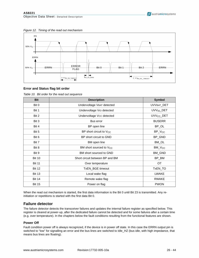
The error flags and the status flags can be read out by applying a clock signal to pin EN in a non low power mode. A falling edge on pin EN starts the read out loading the content of the error/status flag into the shift register and signaling the error flag on the ERRN pin. On the second falling edge the first flag (Bit 0) will be shifted out. The ERRN data is valid after tRO_EN_ERRN. If EN pin keeps on toggling after last flag (Bit 15) the next flag shifted out is Bit 0. The complete list of bits is shown in Table 10. If no transition is detected on pin EN for longer than tRO_EN_TIMEOUT the device enters the operation mode indicated by the host pins.
Table 9. Read Out Mechanism and Transceiver States
State Enabled/Disabled
NORMAL mode Enabled
RECEIVE ONLY mode Enabled
STANDBY mode Disabled
GO TO SLEEP mode Disabled
SLEEP mode Disabled
www.austriamicrosystems.com Revision 17732-005-10a 25 - 44
AS8221Objective Data Sheet - De ta i led Descr ip t ion
Figure 12. Timing of the read out mechanism
Error and Status flag bit order
When the read out mechanism is started, the first data information is the Bit 0 until Bit 23 is transmitted. Any re-initiation or repetitions is started with the first data Bit 0.
Failure detectorThe failure detector detects the transceiver failures and updates the internal failure register as specified below. This register is cleared at power-up, after the dedicated failure cannot be detected and for some failures after a certain time (e.g. over temperature). In the chapters below the fault conditions resulting from the functional features are shown.
Power OffFault condition power off is always recognized, if the device is in power off state. In this case the ERRN output pin is switched to “low” for signalling an error and the bus lines are switched to Idle_HZ (bus idle, with high impedance, that means bus lines are floating).
Table 10. Bit order for the read out sequence
Bit Description Symbol
Bit 0 Undervoltage VBAT detected UVVBAT_DET
Bit 1 Undervoltage VIO detected UVVIO_DET
Bit 2 Undervoltage VCC detected UVVCC_DET
Bit 3 Bus error BUSERR
Bit 4 BP open line BP_OL
Bit 5 BP short circuit to VCC BP_VCC
Bit 6 BP short circuit to GND BP_GND
Bit 7 BM open line BM_OL
Bit 8 BM short sourced to VCC BM_VCC
Bit 9 BM short sourced to GND BM_GND
Bit 10 Short circuit between BP and BM BP_BM
Bit 11 Over temperature OT
Bit 12 TxEN_BGE timeout TxEN_TO
Bit 13 Local wake flag LWAKE
Bit 14 Remote wake flag RWAKE
Bit 15 Power on flag PWON
EN
ERRN
50% VIO
ERROR FLAG Bit 0 Bit 1 Bit 2
t < tRO_EN_TIMEOUTtRO_EN_ERRN t > tRO_EN__TIMEOUT
ERRNERRN50% VIO
www.austriamicrosystems.com Revision 17732-005-10a 26 - 44
AS8221Objective Data Sheet - De ta i led Descr ip t ion
Undervoltage VBAT
Whenever the undervoltage VBAT flag is set, the bus lines are in Idle_LP (idle low power) and the ERRN is switched to “low” for signalling an error. Vice versa, the error is not signalled on the ERRN pin, when the flag is not set.
Undervoltage VCC
Whenever the undervoltage VCC flag is set, the bus lines are in Idle_LP (idle low power) and the ERRN is switched to “low” for signalling an error. Vice versa, the error is not signalled on the ERRN pin, when the flag is not set.
Undervoltage VIO
Whenever the undervoltage VIO flag is set, the bus lines are in Idle_LP (idle low power) and the ERRN is switched to “low” for signalling an error. Vice versa, the error is not signalled on the ERRN pin, when the flag is not set.
Bus Error (Short circuit/open load on bus lines and short circuit between BP and BM)Short circuit on bus lines comprises the 10 flags for high current flags on BP and BM and the flag for detecting short circuit between the bus lines. Whenever on of these flags is set, an error is signalled on the ERRN pin. For high current detection, the current is limited for the bus lines.
TxD interruptedIf the TxD line is interrupted, Data0 is signalled on the bus lines.
TxEN timeoutWhenever the TxEN timeout flag is set, the bus lines are switched into Idle or Idle_LP
Over temperatureWhenever the over temperature flag is set, the bus lines are switched into Idle or Idle_LP.
No mode changeWhenever the no mode change flag is set, an error is indicated on the ERRN pin.
www.austriamicrosystems.com Revision 17732-005-10a 27 - 44
AS8221Objective Data Sheet - De ta i led Descr ip t ion
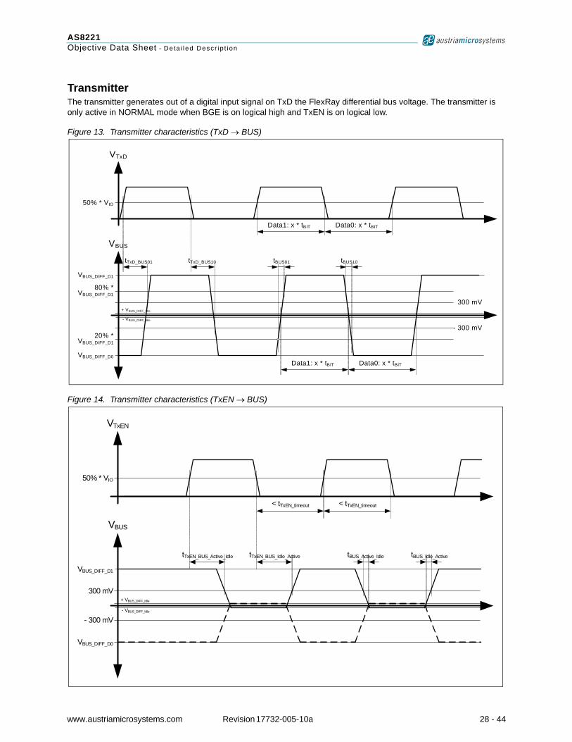
TransmitterThe transmitter generates out of a digital input signal on TxD the FlexRay differential bus voltage. The transmitter is only active in NORMAL mode when BGE is on logical high and TxEN is on logical low.
Figure 13. Transmitter characteristics (TxD → BUS)
Figure 14. Transmitter characteristics (TxEN → BUS)
VTxD
VBUS
- VBUS_DIFF_Idle
+ VBUS_DIFF_Idle
VBUS_DIFF_D1
VBUS_DIFF_D0
tTxD_BUS01 tTxD_BUS10 tBUS01 tBUS10
Data1: x * tBIT Data0: x * tBIT
Data1: x * tBIT Data0: x * tBIT
50% * VIO
80% * VBUS_DIFF_D1
300 mV
- 300 mV20% *
VBUS_DIFF_D1
VTxEN
VBUS
- VBUS_DIFF_Idle
+ VBUS_DIFF_Idle
VBUS_DIFF_D1
VBUS_DIFF_D0
tTxEN_BUS_Active_Idle tBUS_Idle_ActivetBUS_Active_Idle
300 mV
- 300 mV
50% * VIO
tTxEN_BUS_Idle_Active
< tTxEN_timeout < tTxEN_timeout
www.austriamicrosystems.com Revision 17732-005-10a 28 - 44
AS8221Objective Data Sheet - De ta i led Descr ip t ion
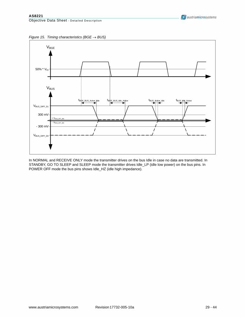
Figure 15. Timing characteristics (BGE → BUS)
In NORMAL and RECEIVE ONLY mode the transmitter drives on the bus Idle in case no data are transmitted. In STANDBY, GO TO SLEEP and SLEEP mode the transmitter drives Idle_LP (idle low power) on the bus pins. In POWER OFF mode the bus pins shows Idle_HZ (idle high impedance).
VBGE
VBUS
- VBUS_DIFF_Idle
+ VBUS_DIFF_Idle
VBUS_DIFF_D1
VBUS_DIFF_D0
tBGE_BUS_Active_Idle tBUS_Idle_ActivetBUS_Active_Idle
300 mV
- 300 mV
50% * VIO
tBGE_BUS_Idle_Active
www.austriamicrosystems.com Revision 17732-005-10a 29 - 44
AS8221Objective Data Sheet - De ta i led Descr ip t ion
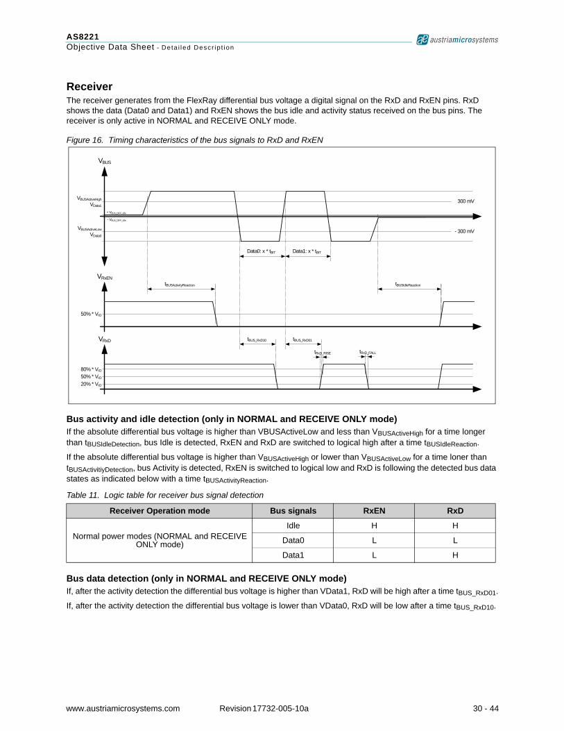
ReceiverThe receiver generates from the FlexRay differential bus voltage a digital signal on the RxD and RxEN pins. RxD shows the data (Data0 and Data1) and RxEN shows the bus idle and activity status received on the bus pins. The receiver is only active in NORMAL and RECEIVE ONLY mode.
Figure 16. Timing characteristics of the bus signals to RxD and RxEN
Bus activity and idle detection (only in NORMAL and RECEIVE ONLY mode)If the absolute differential bus voltage is higher than VBUSActiveLow and less than VBUSActiveHigh for a time longer than tBUSIdleDetection, bus Idle is detected, RxEN and RxD are switched to logical high after a time tBUSIdleReaction.
If the absolute differential bus voltage is higher than VBUSActiveHigh or lower than VBUSActiveLow for a time loner than tBUSActivitiyDetection, bus Activity is detected, RxEN is switched to logical low and RxD is following the detected bus data states as indicated below with a time tBUSActivityReaction.
Bus data detection (only in NORMAL and RECEIVE ONLY mode)If, after the activity detection the differential bus voltage is higher than VData1, RxD will be high after a time tBUS_RxD01.
If, after the activity detection the differential bus voltage is lower than VData0, RxD will be low after a time tBUS_RxD10.
Table 11. Logic table for receiver bus signal detection
Receiver Operation mode Bus signals RxEN RxD
Normal power modes (NORMAL and RECEIVE ONLY mode)
Idle H H
Data0 L L
Data1 L H
VBUS
- VBUS_DIFF_Idle
+ VBUS_DIFF_Idle
tRxD_FALL
VBUSActiveHighVData1
VBUSActiveLowVData0
VRxEN
50% * VIO
VRxD
20% * VIO
80% * VIO
tBUSActivityReaction
tBUS_RxD10 tBUS_RxD01
tRxD_RISE
tBUSIdleReaction
Data0: x * tBIT Data1: x * tBIT
50% * VIO
300 mV
- 300 mV
www.austriamicrosystems.com Revision 17732-005-10a 30 - 44
AS8221Objective Data Sheet - De ta i led Descr ip t ion
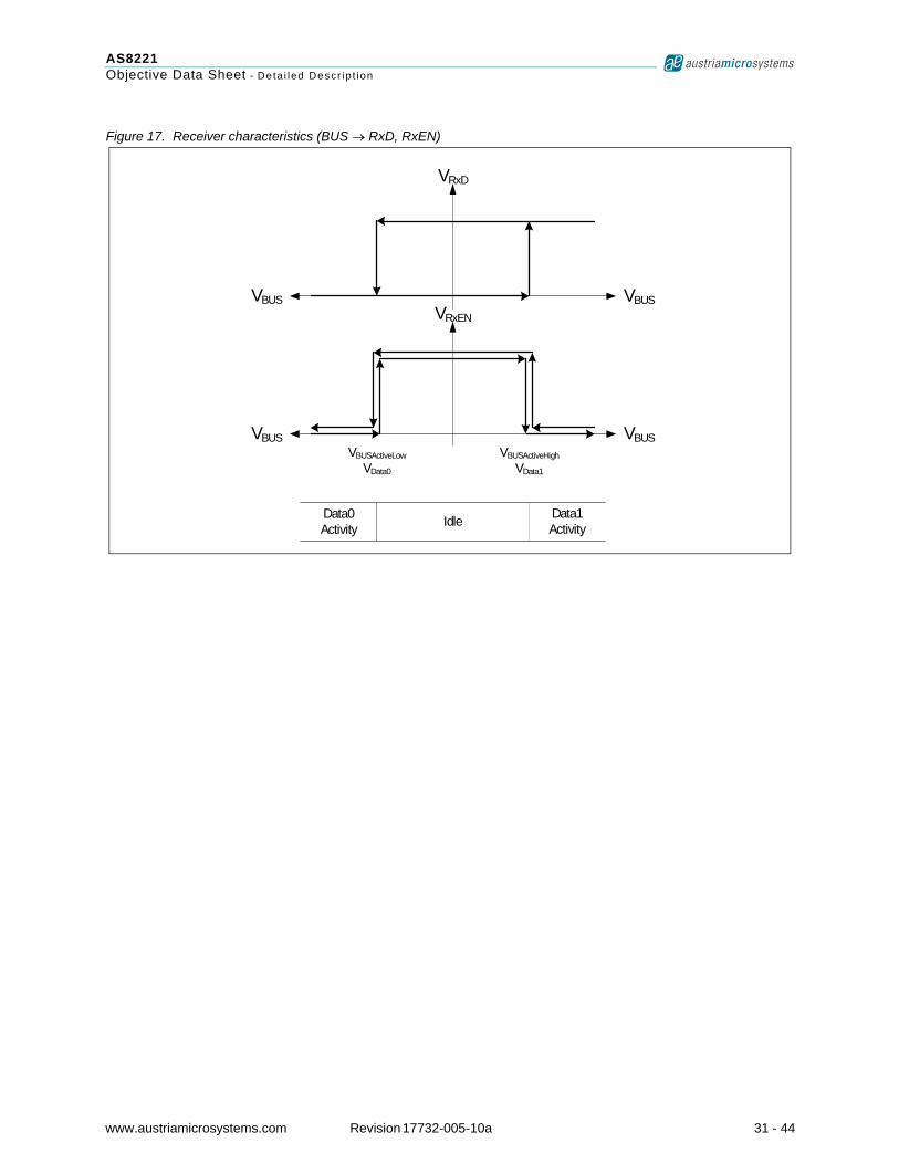
Figure 17. Receiver characteristics (BUS → RxD, RxEN)
VRxD
VBUS
VBUSActiveLowVData0
VBUSActiveHighVData1
Data0Activity Idle Data1
Activity
VRxEN
VBUSVBUS
VBUS
www.austriamicrosystems.com Revision 17732-005-10a 31 - 44
AS8221Objective Data Sheet - De ta i led Descr ip t ion
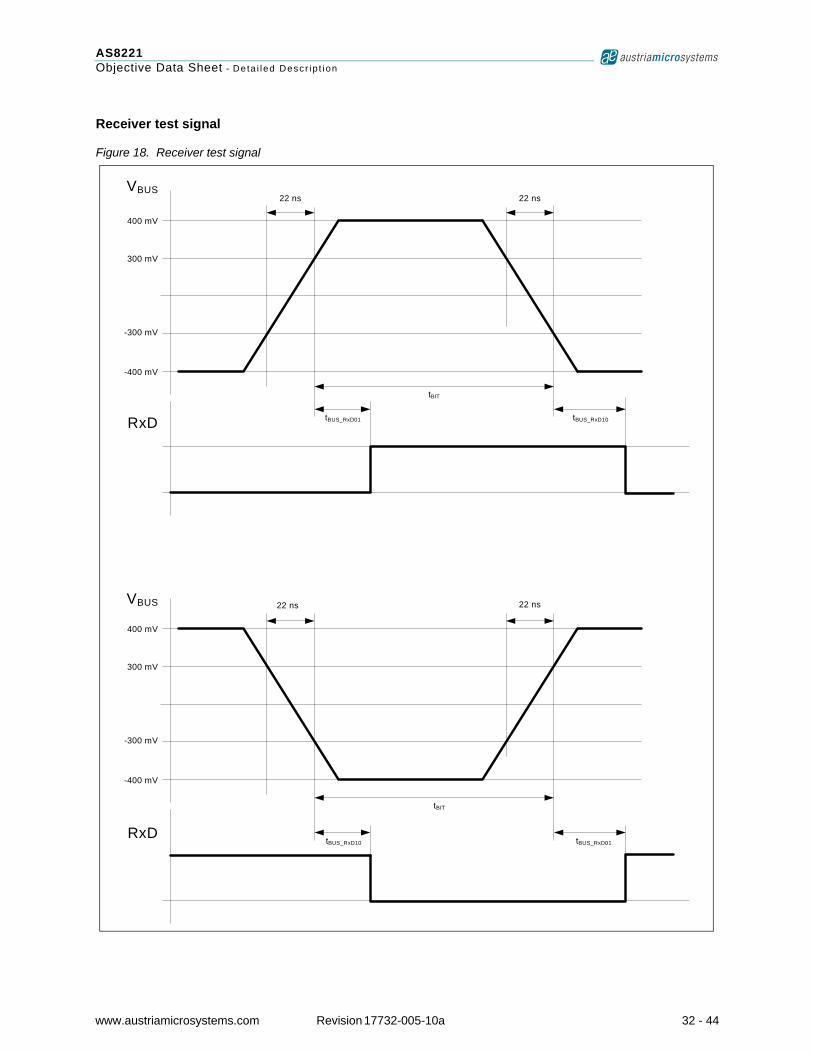
Receiver test signal
Figure 18. Receiver test signal
22 ns 22 ns
tBIT
tBUS_RxD01 tBUS_RxD10
VBUS
RxD
tBUS_RxD10
VBUS
RxD
22 ns 22 ns
400 mV
300 mV
-300 mV
-400 mV
400 mV
300 mV
-300 mV
-400 mV
tBIT
tBUS_RxD01
www.austriamicrosystems.com Revision 17732-005-10a 32 - 44
AS8221Objective Data Sheet - De ta i led Descr ip t ion
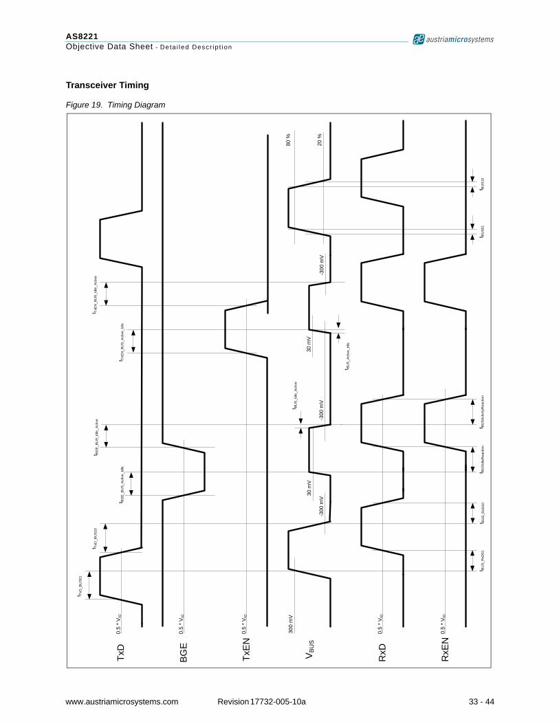
Transceiver Timing
Figure 19. Timing Diagram
TxD
BGE
TxE
N
VB
US
RxD
RxE
N
0.5
* VIO
300
mV
30 m
V
80 %
20 %
t TxE
N_B
US_
Act
ive_
Idle
t TxE
N_B
US
_Idl
e_A
ctiv
e
t BG
E_B
US
_Act
ive_
Idle
t BG
E_BU
S_I
dle_
Act
ive
t TxD
_BU
S01
t TxD
_BU
S10
t BU
S_R
xD01
t BU
S_R
xD10
t BU
SIdl
eRea
ctio
nt B
USA
ctiv
ityR
eact
ion
t BU
S01
t BU
S10
30 m
V
-300
mV
-300
mV
-300
mV
t BU
S_I
dle_
Act
ive
t BU
S_Ac
tive_
Idle
0.5
* VIO
0.5
* VIO
0.5
* VIO
0.5
* VIO
www.austriamicrosystems.com Revision 17732-005-10a 33 - 44
AS8221Objective Data Sheet - De ta i led Descr ip t ion
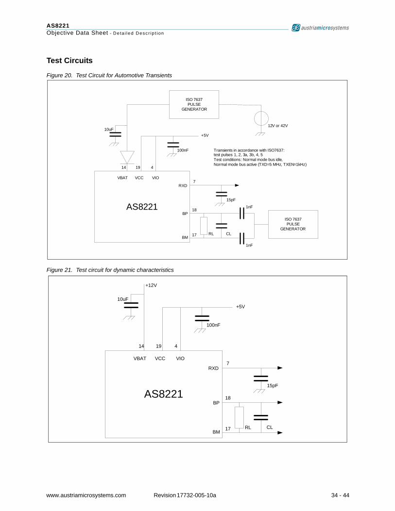
Test Circuits
Figure 20. Test Circuit for Automotive Transients
Figure 21. Test circuit for dynamic characteristics
AS8221
RXD
BP
BMRL CL
15pF
VBAT VCC VIO
100nF
+5V10uF
14 19 4
7
18
17
1nF
1nF
ISO 7637PULSE
GENERATOR
ISO 7637PULSE
GENERATOR
12V or 42V
Transients in accordance with ISO7637:test pulses 1, 2, 3a, 3b, 4, 5Test conditions: Normal mode bus idle, Normal mode bus active (TXD=5 MHz, TXEN=1kHz)
AS8221
RXD
BP
BMRL CL
15pF
VBAT VCC VIO
100nF
+5V
+12V
10uF
14 19 4
7
18
17
www.austriamicrosystems.com Revision 17732-005-10a 34 - 44
AS8221Objective Data Sheet - Append ix
9 AppendixFlexRay Functional ClassesThe AS8221 device comprises following Functional Classes according the FlexRay Electrical Physical Layer Specification V2.1 Rev. B: Functional Class “BD Voltage Regulator Control” Functional Class “Bus Driver - Bus Guardian Control Interface” Functional Class “Bus Driver Internal Voltage Regulator” Functional Class “Bus Driver Logic Level Adaptation”
FlexRay Parameter ComparisonThe following table shows the comparison of conventions used in AS8221 datasheet and FlexRay Electrical Physical Layer Specification V2.1 Rev. B.
Table 12. Comparison table
AS8221C Datasheet FlexRayElectrical Physical Layer Specification V2.1 Rev. B
Symbol Parameter Name DescriptionAbsolute Maximum Ratings
- Battery Supply Voltage (VBAT) - -
- Supply Voltage (VCC) - -
- Supply Voltage (VIO) - -
- DC Voltage at EN, STBN, ERRN, TxD, RxD, TxEN, BGE, RxEN - -
- DC Voltage on pin WAKE, INH1, INH2 - -
- DC Voltage at BP and BM - -
- Input current (latchup immunity) - -
- Electrostatic discharge at bus lines BP, BM, VBAT, WAKE uESDExt ESD protection on pins that lead to
ECU external terminals
- Electrostatic discharge uESDint ESD on all other pins
- Transient voltage on BP, BM - -
- Transient voltage on VBAT - -
- Total power dissipation (all supplies and outputs) - -
- Storage temperature - -
- Junction temperature - -
- Package body temperature - -
- Humidity non-condensing - -Supply Voltage
Tamb Ambient temperature T Ambient temperature
VCC - VIO Difference of supplies - -
IBAT VBAT current consumption - -
www.austriamicrosystems.com Revision 17732-005-10a 35 - 44
AS8221Objective Data Sheet - Append ix
ICC VCC current consumption - -
IIO VIO current consumption - -
State Transitions
tSTBN_RxDDelay STBN high to RxD high with
wake flag set - -
tSTBN_RxENDelay STBN high to RxEN high with
wake flag set - -
tSLEEP_INH1 Delay STBN high to INH1 high - -
tSTANDBY_INH2 Delay STBN high to INH2 high - -
tSLEEP go-to-sleep hold time - -
Transmitter
VBUS_DIFF_D0Differential bus voltage low in
NORMAL mode (Data0) uBDTxactive Absolute value of uBus while sending
VBUS_DIFF_D1Differential bus voltage high in
NORMAL mode (Data1) uBDTxactive Absolute value of uBus while sending
VBUS_DIFFMatching between Data0 and Data1differential bus voltage in NORMAL
mode- -
VBUS_COM_D0Common mode bus voltage in case of
Data0 in non low power modes - -
VBUS_COM_D1Common mode bus voltage in case of
Data1 in non low power modes - -
VBUS_COMMatching between Data0 and Data1
common mode voltage - -
VBUS_DIFF_IdleAbsolute differential bus voltage in
idle mode uBDTxidle Absolute value of uBus, while Idle
IBPBMShortMaxIBMBPShortMax
Absolute max current when BP is shorted to BM
IBPBMShortMaxIBMBPShortMax
Absolute maximum output current when BP shorted to BM
IBPGNDShortMaxAbsolute max current when BP is
shorted to GND IBPGNDShortMaxAbsolute maximum output current
when shorted to GND
IBMGNDShortMaxAbsolute max current when BM is
shorted to GND IBMGNDShortMaxAbsolute maximum output current
when shorted to GND
IBP-5VShortMaxAbsolute max current when BP is
shorted to -5 V IBP-5VShortMaxAbsolute maximum output current
when shorted to -5V
IBM-5VShortMaxAbsolute max current when BM is
shorted to -5 V IBM-5VShortMax Absolute maximum output current
when shorted to -5V
IBP27VShortMaxAbsolute max current when BP is
shorted to 27 V IBPBAT27VShortMaxAbsolute maximum output current
when shorted to 27V
Table 12. Comparison table
AS8221C Datasheet FlexRayElectrical Physical Layer Specification V2.1 Rev. B
Symbol Parameter Name Description
www.austriamicrosystems.com Revision 17732-005-10a 36 - 44
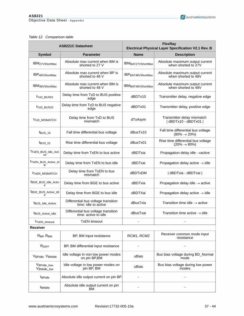
AS8221Objective Data Sheet - Append ix
IBM27VShortMaxAbsolute max current when BM is
shorted to 27 V IBMBAT27VShortMaxAbsolute maximum output current
when shorted to 27V
IBP48VShortMaxAbsolute max current when BP is
shorted to 48 V IBPBAT48VShortMaxAbsolute maximum output current
when shorted to 48V
IBM48VShortMaxAbsolute max current when BM is
shorted to 48 V IBMBAT48VShortMaxAbsolute maximum output current
when shorted to 48V
tTxD_BUS01Delay time from TxD to BUS positive
edge dBDTx10 Transmitter delay, negative edge
tTxD_BUS10Delay time from TxD to BUS negative
edge dBDTx01 Transmitter delay, positive edge
tTxD_MISMATCHDelay time from TxD to BUS
mismatch dTxAsym Transmitter delay mismatch | dBDTx10 - dBDTx01 |
tBUS_10 Fall time differential bus voltage dBusTx10 Fall time differential bus voltage (80% → 20%)
tBUS_01 Rise time differential bus voltage dBusTx01 Rise time differential bus voltage (20% → 80%)
tTxEN_BUS_Idle_Active Delay time from TxEN to bus active dBDTxia Propagation delay idle →active
tTxEN_BUS_Active_Idle Delay time from TxEN to bus idle dBDTxai Propagation delay active → idle
tTxEN_MISMATCHDelay time from TxEN to bus
mismatch dBDTxDM | dBDTxia - dBDTxai |
tBGE_BUS_Idle_Active Delay time from BGE to bus active dBDTxia Propagation delay idle → active
tBGE_BUS_Active_Idle Delay time from BGE to bus idle dBDTXai Propagation delay active → idle
tBUS_Idle_ActiveDifferential bus voltage transition
time: idle to active dBusTxia Transition time idle → active
tBUS_Active_IdleDifferential bus voltage transition
time: active to idle dBusTxai Transition time active → idle
tTxEN_timeout TxEN timeout - -
Receiver
RBP, RBM BP, BM input resistance RCM1, RCM2 Receiver common mode input resistance
RDIFF BP, BM differential input resistance - -
VBPidle, VBMidleIdle voltage in non low power modes
on pin BP,BM uBias Bus bias voltage during BD_Normal mode
VBPidle_low, VBMidle_low
Idle voltage in low power modes on pin BP, BM uBias Bus bias voltage during low power
modes
IBPidle Absolute idle output current on pin BP - -
IBMidleAbsolute idle output current on pin
BM - -
Table 12. Comparison table
AS8221C Datasheet FlexRayElectrical Physical Layer Specification V2.1 Rev. B
Symbol Parameter Name Description
www.austriamicrosystems.com Revision 17732-005-10a 37 - 44
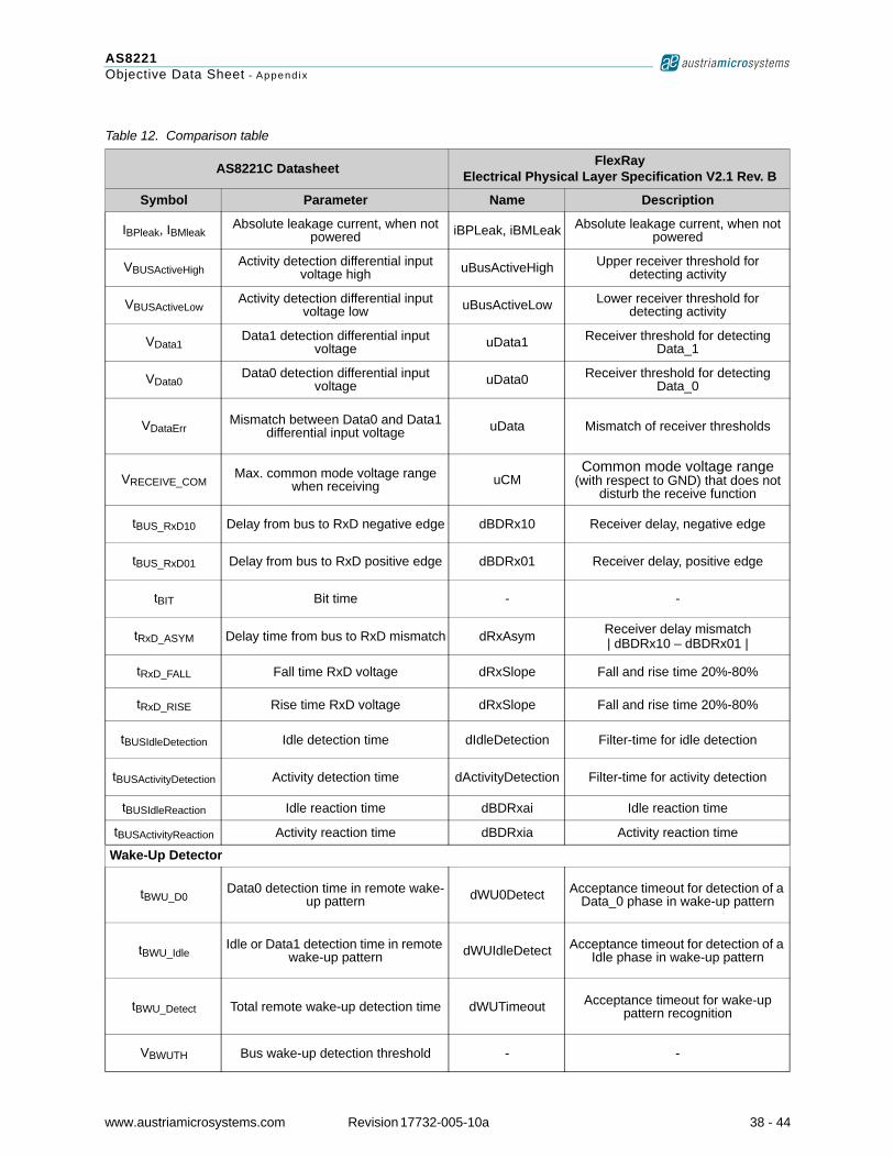
AS8221Objective Data Sheet - Append ix
IBPleak, IBMleakAbsolute leakage current, when not
powered iBPLeak, iBMLeak Absolute leakage current, when not powered
VBUSActiveHighActivity detection differential input
voltage high uBusActiveHigh Upper receiver threshold for detecting activity
VBUSActiveLowActivity detection differential input
voltage low uBusActiveLow Lower receiver threshold for detecting activity
VData1Data1 detection differential input
voltage uData1 Receiver threshold for detecting Data_1
VData0Data0 detection differential input
voltage uData0 Receiver threshold for detecting Data_0
VDataErrMismatch between Data0 and Data1
differential input voltage uData Mismatch of receiver thresholds
VRECEIVE_COMMax. common mode voltage range
when receiving uCMCommon mode voltage range
(with respect to GND) that does not disturb the receive function
tBUS_RxD10 Delay from bus to RxD negative edge dBDRx10 Receiver delay, negative edge
tBUS_RxD01 Delay from bus to RxD positive edge dBDRx01 Receiver delay, positive edge
tBIT Bit time - -
tRxD_ASYM Delay time from bus to RxD mismatch dRxAsym Receiver delay mismatch | dBDRx10 – dBDRx01 |
tRxD_FALL Fall time RxD voltage dRxSlope Fall and rise time 20%-80%
tRxD_RISE Rise time RxD voltage dRxSlope Fall and rise time 20%-80%
tBUSIdleDetection Idle detection time dIdleDetection Filter-time for idle detection
tBUSActivityDetection Activity detection time dActivityDetection Filter-time for activity detection
tBUSIdleReaction Idle reaction time dBDRxai Idle reaction time
tBUSActivityReaction Activity reaction time dBDRxia Activity reaction time
Wake-Up Detector
tBWU_D0Data0 detection time in remote wake-
up pattern dWU0Detect Acceptance timeout for detection of a Data_0 phase in wake-up pattern
tBWU_IdleIdle or Data1 detection time in remote
wake-up pattern dWUIdleDetect Acceptance timeout for detection of a Idle phase in wake-up pattern
tBWU_Detect Total remote wake-up detection time dWUTimeout Acceptance timeout for wake-up pattern recognition
VBWUTH Bus wake-up detection threshold - -
Table 12. Comparison table
AS8221C Datasheet FlexRayElectrical Physical Layer Specification V2.1 Rev. B
Symbol Parameter Name Description
www.austriamicrosystems.com Revision 17732-005-10a 38 - 44
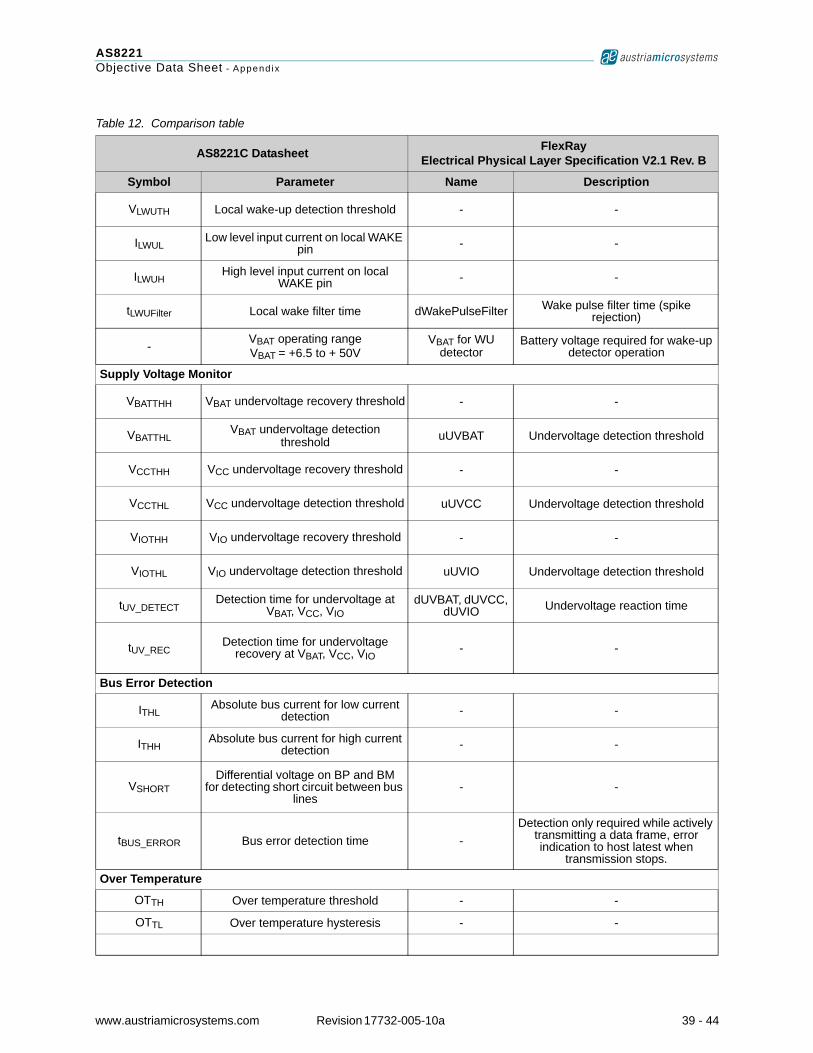
AS8221Objective Data Sheet - Append ix
VLWUTH Local wake-up detection threshold - -
ILWULLow level input current on local WAKE
pin - -
ILWUHHigh level input current on local
WAKE pin - -
tLWUFilter Local wake filter time dWakePulseFilter Wake pulse filter time (spike rejection)
- VBAT operating rangeVBAT = +6.5 to + 50V
VBAT for WU detector
Battery voltage required for wake-up detector operation
Supply Voltage Monitor
VBATTHH VBAT undervoltage recovery threshold - -
VBATTHLVBAT undervoltage detection
threshold uUVBAT Undervoltage detection threshold
VCCTHH VCC undervoltage recovery threshold - -
VCCTHL VCC undervoltage detection threshold uUVCC Undervoltage detection threshold
VIOTHH VIO undervoltage recovery threshold - -
VIOTHL VIO undervoltage detection threshold uUVIO Undervoltage detection threshold
tUV_DETECTDetection time for undervoltage at
VBAT, VCC, VIOdUVBAT, dUVCC,
dUVIO Undervoltage reaction time
tUV_RECDetection time for undervoltage
recovery at VBAT, VCC, VIO- -
Bus Error Detection
ITHLAbsolute bus current for low current
detection - -
ITHHAbsolute bus current for high current
detection - -
VSHORTDifferential voltage on BP and BM
for detecting short circuit between bus lines
- -
tBUS_ERROR Bus error detection time -Detection only required while actively
transmitting a data frame, error indication to host latest when
transmission stops.Over Temperature
OTTH Over temperature threshold - -
OTTL Over temperature hysteresis - -
Table 12. Comparison table
AS8221C Datasheet FlexRayElectrical Physical Layer Specification V2.1 Rev. B
Symbol Parameter Name Description
www.austriamicrosystems.com Revision 17732-005-10a 39 - 44
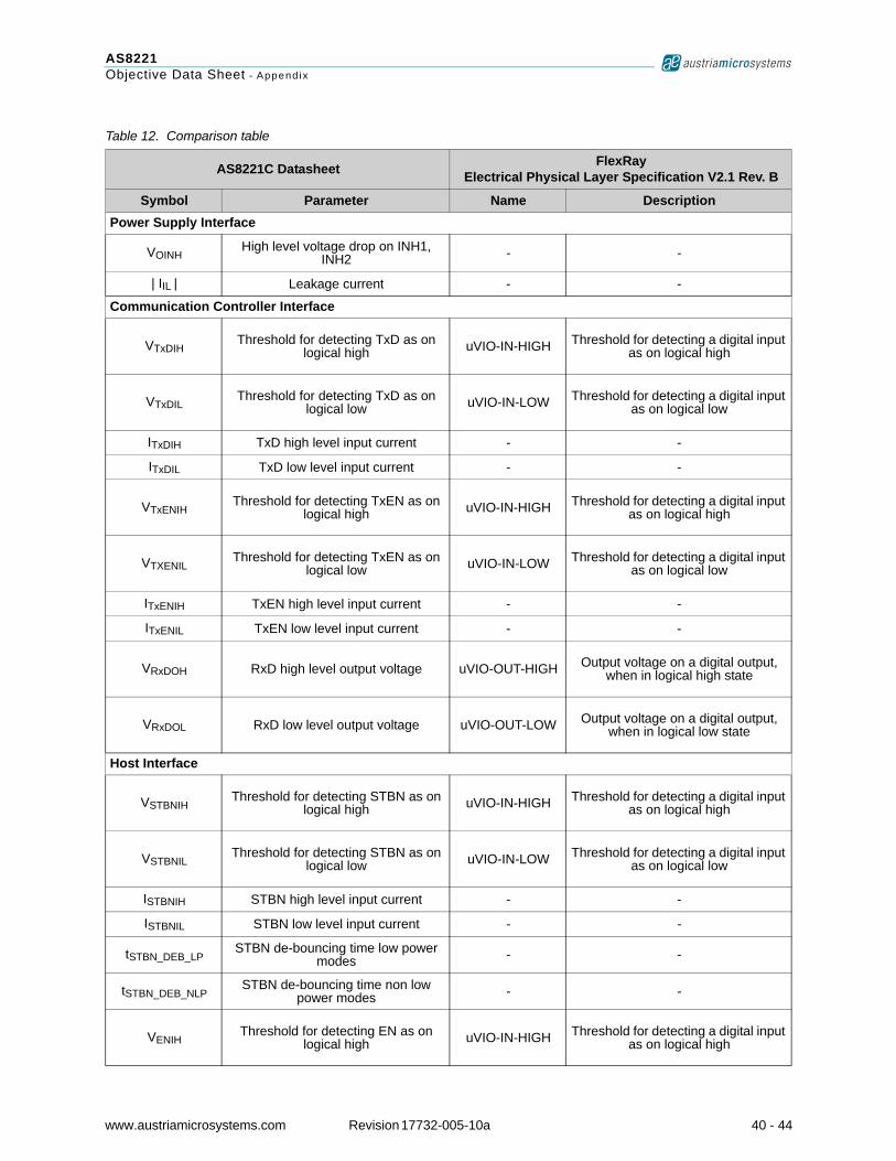
AS8221Objective Data Sheet - Append ix
Power Supply Interface
VOINHHigh level voltage drop on INH1,
INH2 - -
| IIL | Leakage current - -
Communication Controller Interface
VTxDIHThreshold for detecting TxD as on
logical high uVIO-IN-HIGH Threshold for detecting a digital input as on logical high
VTxDILThreshold for detecting TxD as on
logical low uVIO-IN-LOW Threshold for detecting a digital input as on logical low
ITxDIH TxD high level input current - -
ITxDIL TxD low level input current - -
VTxENIHThreshold for detecting TxEN as on
logical high uVIO-IN-HIGH Threshold for detecting a digital input as on logical high
VTXENILThreshold for detecting TxEN as on
logical low uVIO-IN-LOW Threshold for detecting a digital input as on logical low
ITxENIH TxEN high level input current - -
ITxENIL TxEN low level input current - -
VRxDOH RxD high level output voltage uVIO-OUT-HIGH Output voltage on a digital output, when in logical high state
VRxDOL RxD low level output voltage uVIO-OUT-LOW Output voltage on a digital output, when in logical low state
Host Interface
VSTBNIHThreshold for detecting STBN as on
logical high uVIO-IN-HIGH Threshold for detecting a digital input as on logical high
VSTBNILThreshold for detecting STBN as on
logical low uVIO-IN-LOW Threshold for detecting a digital input as on logical low
ISTBNIH STBN high level input current - -
ISTBNIL STBN low level input current - -
tSTBN_DEB_LPSTBN de-bouncing time low power
modes - -
tSTBN_DEB_NLPSTBN de-bouncing time non low
power modes - -
VENIHThreshold for detecting EN as on
logical high uVIO-IN-HIGH Threshold for detecting a digital input as on logical high
Table 12. Comparison table
AS8221C Datasheet FlexRayElectrical Physical Layer Specification V2.1 Rev. B
Symbol Parameter Name Description
www.austriamicrosystems.com Revision 17732-005-10a 40 - 44
AS8221Objective Data Sheet - Append ix
VENILThreshold for detecting EN as on
logical low uVIO-IN-LOW Threshold for detecting a digital input as on logical low
IENIH EN high level input current - -
IENIL EN low level input current - -
tEN_DEB_LPEN de-bouncing time low power
modes - -
tEN_DEB_NLPEN de-bouncing time non low power
modes - -
VERRNOH ERRN high level output voltage uVIO-OUT-HIGH Output voltage on a digital output, when in logical high state
VERRNOL ERRN low level output voltage uVIO-OUT-LOW Output voltage on a digital output, when in logical low state
Bus Guardian Interface
VBGEIHThreshold for detecting BGE as on
logical high uVIO-IN-HIGH Threshold for detecting a digital input as on logical high
VBGEILThreshold for detecting BGE as on
logical low uVIO-IN-LOW Threshold for detecting a digital input as on logical low
IBGEIH BGE high level input current - -
IBGEIL BGE low level input current - -
VRXENOH RxEN high level output voltage uVIO-OUT-HIGH Output voltage on a digital output, when in logical high state
VRXENOL RxEN low level output voltage uVIO-OUT-LOW Output voltage on a digital output, when in logical low state
Read Out Interface
tRO_EN_ERRNPropagation delay falling edge EN to
ERRN - -
tRO_EN_TIMEOUT Error read out time out - -
Table 12. Comparison table
AS8221C Datasheet FlexRayElectrical Physical Layer Specification V2.1 Rev. B
Symbol Parameter Name Description
www.austriamicrosystems.com Revision 17732-005-10a 41 - 44
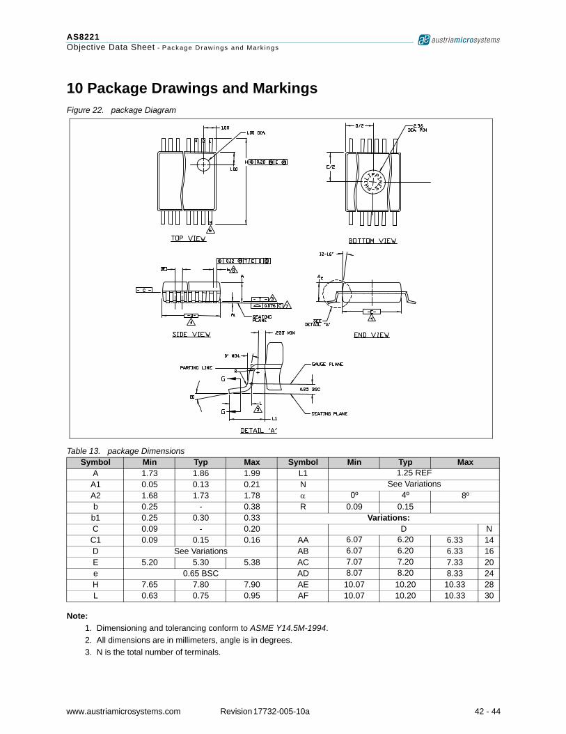
AS8221Objective Data Sheet - Package Drawings and Mark ings
10 Package Drawings and MarkingsFigure 22. package Diagram
Note:1. Dimensioning and tolerancing conform to ASME Y14.5M-1994.2. All dimensions are in millimeters, angle is in degrees.3. N is the total number of terminals.
Table 13. package DimensionsSymbol Min Typ Max Symbol Min Typ Max
A 1.73 1.86 1.99 L1 1.25 REFA1 0.05 0.13 0.21 N See VariationsA2 1.68 1.73 1.78 α 0º 4º 8ºb 0.25 - 0.38 R 0.09 0.15
b1 0.25 0.30 0.33 Variations:C 0.09 - 0.20 D NC1 0.09 0.15 0.16 AA 6.07 6.20 6.33 14D See Variations AB 6.07 6.20 6.33 16E 5.20 5.30 5.38 AC 7.07 7.20 7.33 20e 0.65 BSC AD 8.07 8.20 8.33 24H 7.65 7.80 7.90 AE 10.07 10.20 10.33 28L 0.63 0.75 0.95 AF 10.07 10.20 10.33 30
www.austriamicrosystems.com Revision 17732-005-10a 42 - 44
AS8221Objective Data Sheet - Order ing In format ion
11 Ordering InformationTable 14. Ordering Information
Type Marking Description Delivery Form Package
www.austriamicrosystems.com Revision 17732-005-10a 43 - 44
AS8221Objective Data Sheet - Order ing In format ion
CopyrightsCopyright © 1997-2008, austriamicrosystems AG, Schloss Premstaetten, 8141 Unterpremstaetten, Austria-Europe. Trademarks Registered ®. All rights reserved. The material herein may not be reproduced, adapted, merged, translated, stored, or used without the prior written consent of the copyright owner.
All products and companies mentioned are trademarks or registered trademarks of their respective companies.
DisclaimerDevices sold by austriamicrosystems AG are covered by the warranty and patent indemnification provisions appearing in its Term of Sale. austriamicrosystems AG makes no warranty, express, statutory, implied, or by description regarding the information set forth herein or regarding the freedom of the described devices from patent infringement. austriamicrosystems AG reserves the right to change specifications and prices at any time and without notice. Therefore, prior to designing this product into a system, it is necessary to check with austriamicrosystems AG for current information. This product is intended for use in normal commercial applications. Applications requiring extended temperature range, unusual environmental requirements, or high reliability applications, such as military, medical life-support or life-sustaining equipment are specifically not recommended without additional processing by austriamicrosystems AG for each application. For shipments of less than 100 parts the manufacturing flow might show deviations from the standard production flow, such as test flow or test location.
The information furnished here by austriamicrosystems AG is believed to be correct and accurate. However, austriamicrosystems AG shall not be liable to recipient or any third party for any damages, including but not limited to personal injury, property damage, loss of profits, loss of use, interruption of business or indirect, special, incidental or consequential damages, of any kind, in connection with or arising out of the furnishing, performance or use of the technical data herein. No obligation or liability to recipient or any third party shall arise or flow out of austriamicrosystems AG rendering of technical or other services.
Contact InformationHeadquartersaustriamicrosystems AG A-8141 Schloss Premstaetten, Austria
Tel: +43 (0) 3136 500 0 Fax: +43 (0) 3136 525 01
For Sales Offices, Distributors and Representatives, please visit:
http://www.austriamicrosystems.com/contact B
www.austriamicrosystems.com Revision 17732-005-10a 44 - 44