Embed Size (px)
Citation preview
AS3935 Frankl in L ightn ing Sensor IC
Datasheet
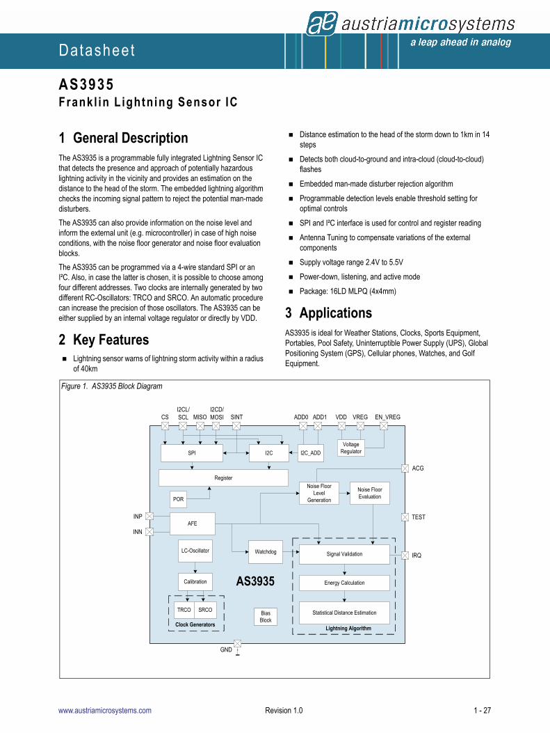
1 General DescriptionThe AS3935 is a programmable fully integrated Lightning Sensor IC that detects the presence and approach of potentially hazardous lightning activity in the vicinity and provides an estimation on the distance to the head of the storm. The embedded lightning algorithm checks the incoming signal pattern to reject the potential man-made disturbers.
The AS3935 can also provide information on the noise level and inform the external unit (e.g. microcontroller) in case of high noise conditions, with the noise floor generator and noise floor evaluation blocks.
The AS3935 can be programmed via a 4-wire standard SPI or an I²C. Also, in case the latter is chosen, it is possible to choose among four different addresses. Two clocks are internally generated by two different RC-Oscillators: TRCO and SRCO. An automatic procedure can increase the precision of those oscillators. The AS3935 can be either supplied by an internal voltage regulator or directly by VDD.
2 Key FeaturesLightning sensor warns of lightning storm activity within a radius
of 40km
Distance estimation to the head of the storm down to 1km in 14 steps
Detects both cloud-to-ground and intra-cloud (cloud-to-cloud) flashes
Embedded man-made disturber rejection algorithm
Programmable detection levels enable threshold setting for optimal controls
SPI and I²C interface is used for control and register reading
Antenna Tuning to compensate variations of the external components
Supply voltage range 2.4V to 5.5V
Power-down, listening, and active mode
Package: 16LD MLPQ (4x4mm)
3 ApplicationsAS3935 is ideal for Weather Stations, Clocks, Sports Equipment, Portables, Pool Safety, Uninterruptible Power Supply (UPS), Global Positioning System (GPS), Cellular phones, Watches, and Golf Equipment.
Figure 1. AS3935 Block Diagram
POR
Register
I2CSPI
Bias Block
Noise Floor Level
Generation
Noise Floor Evaluation
Signal ValidationWatchdog
Statistical Distance Estimation
LC-Oscillator
Calibration
TRCO SRCO
I2C_ADD
VDD VREG
ACG
IRQ
GND
EN_VREGI2CD/MOSIMISO
I2CL/SCLCS
Lightning Algorithm
Energy Calculation
ADD0 ADD1SINT
INP
INNAFE
TEST
Clock Generators
AS3935
Voltage Regulator
www.austriamicrosystems.com Revision 1.0 1 - 27
AS3935Datasheet - C o n t e n t s
Contents
1 General Description .................................................................................................................................................................. 1
2 Key Features............................................................................................................................................................................. 1
3 Applications............................................................................................................................................................................... 1
4 Pin Assignments ....................................................................................................................................................................... 3
4.1 Pin Descriptions.................................................................................................................................................................................... 3
5 Absolute Maximum Ratings ...................................................................................................................................................... 4
6 Electrical Characteristics........................................................................................................................................................... 5
6.1 Operating Conditions............................................................................................................................................................................ 5
6.2 DC/AC Characteristics for Digital Inputs and Outputs .......................................................................................................................... 5
6.3 Detailed System and Block Specification ............................................................................................................................................. 5
7 Typical Operating Characteristics ............................................................................................................................................. 7
8 Detailed Description.................................................................................................................................................................. 8
8.1 Circuit ................................................................................................................................................................................................. 11
8.2 Operating Modes ................................................................................................................................................................................ 11
8.3 System and Block Specification ......................................................................................................................................................... 11
8.3.1 Register Table ........................................................................................................................................................................... 11
8.3.2 Register Table Description and Default Value........................................................................................................................... 12
8.4 Serial Peripheral Interface (SPI)......................................................................................................................................................... 14
8.4.1 SPI Command Structure............................................................................................................................................................ 14
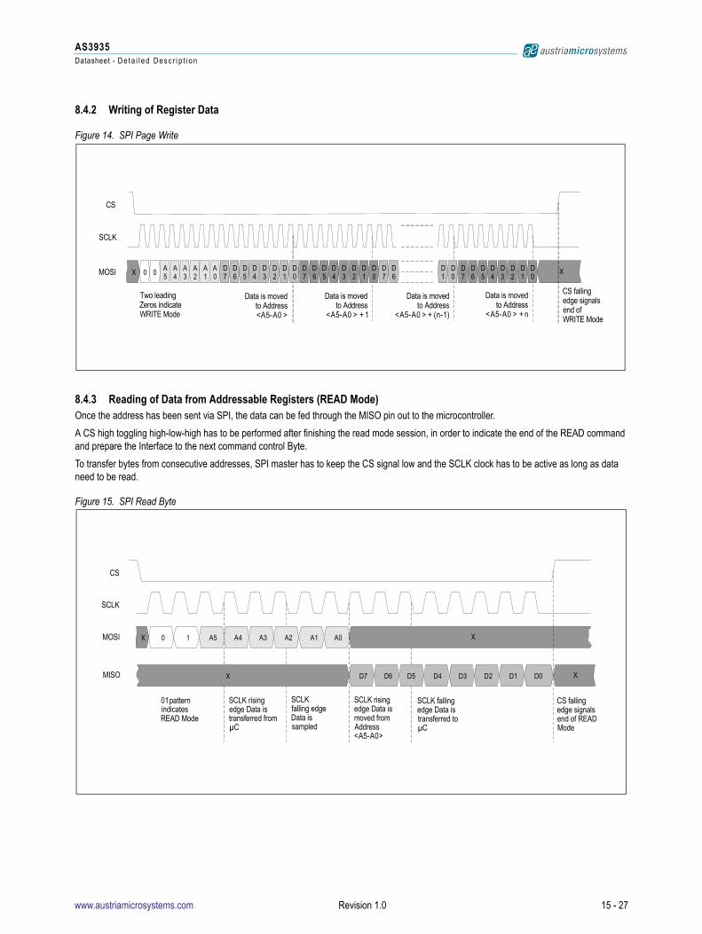
8.4.2 Writing of Register Data............................................................................................................................................................. 15
8.4.3 Reading of Data from Addressable Registers (READ Mode) .................................................................................................... 15
8.4.4 Send Direct Command Byte ...................................................................................................................................................... 16
8.5 I²C....................................................................................................................................................................................................... 16
8.5.1 I²C Byte Write ............................................................................................................................................................................ 17
8.5.2 I²C Register Read ...................................................................................................................................................................... 18
8.5.3 Direct Command........................................................................................................................................................................ 18
8.6 Voltage Regulator ............................................................................................................................................................................... 18
8.7 Analog Front-end (AFE) and Watchdog ............................................................................................................................................. 19
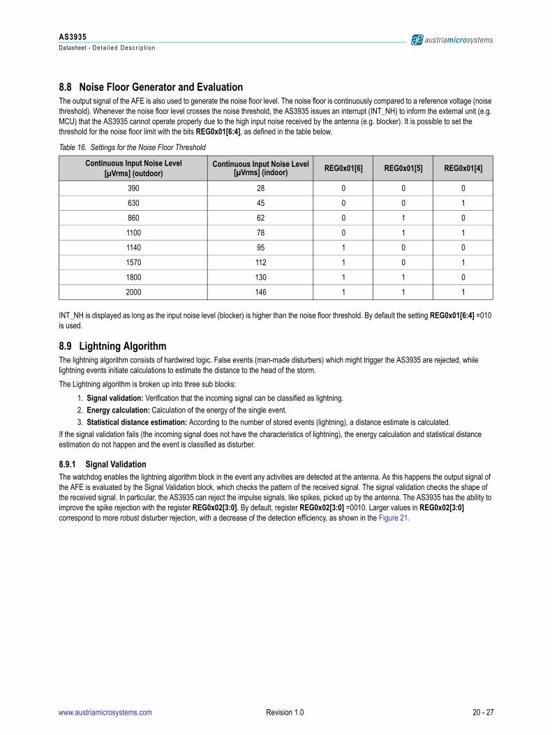
8.8 Noise Floor Generator and Evaluation ............................................................................................................................................... 20
8.9 Lightning Algorithm ............................................................................................................................................................................ 20
8.9.1 Signal Validation ........................................................................................................................................................................ 20
8.9.2 Energy Calculation..................................................................................................................................................................... 21
8.9.3 Statistical Distance Estimation................................................................................................................................................... 21
8.9.4 Interrupt Management ............................................................................................................................................................... 22
8.10 Antenna Tuning ................................................................................................................................................................................ 23
8.11 Clock Generation .............................................................................................................................................................................. 23
9 Package Drawings and Markings ........................................................................................................................................... 24
10 Ordering Information............................................................................................................................................................. 26
www.austriamicrosystems.com Revision 1.0 2 - 27
AS3935Datasheet - P i n A s s i g n m e n t s
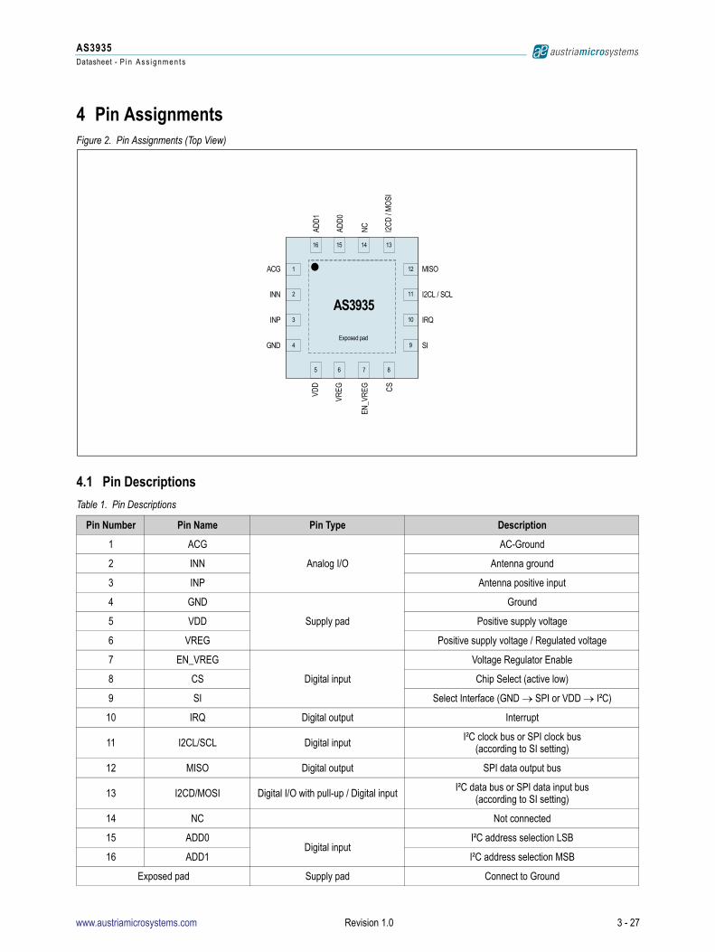
4 Pin AssignmentsFigure 2. Pin Assignments (Top View)
4.1 Pin Descriptions
Table 1. Pin Descriptions
Pin Number Pin Name Pin Type Description
1 ACG
Analog I/O
AC-Ground
2 INN Antenna ground
3 INP Antenna positive input
4 GND
Supply pad
Ground
5 VDD Positive supply voltage
6 VREG Positive supply voltage / Regulated voltage
7 EN_VREG
Digital input
Voltage Regulator Enable
8 CS Chip Select (active low)
9 SI Select Interface (GND SPI or VDD I²C)
10 IRQ Digital output Interrupt
11 I2CL/SCL Digital input I²C clock bus or SPI clock bus(according to SI setting)
12 MISO Digital output SPI data output bus
13 I2CD/MOSI Digital I/O with pull-up / Digital input I²C data bus or SPI data input bus(according to SI setting)
14 NC Not connected
15 ADD0Digital input
I²C address selection LSB
16 ADD1 I²C address selection MSB
Exposed pad Supply pad Connect to Ground
16
1
2
3
4
12
11
10
9
15 14 13
5 6 7 8
AS3935
ACG
INN
INP
GND
VDD
VREG
EN_V
REG C
S
SI
IRQ
I2CL / SCL
MISO
I2C
D /
MO
SI
NC
ADD
0
ADD
1
Exposed pad
www.austriamicrosystems.com Revision 1.0 3 - 27
AS3935Datasheet - A b s o l u t e M a x i m u m R a t i n g s
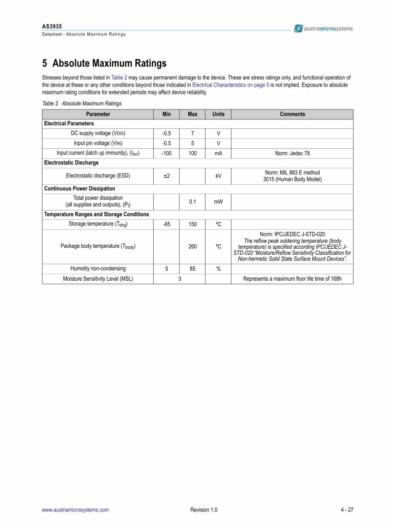
5 Absolute Maximum RatingsStresses beyond those listed in Table 2 may cause permanent damage to the device. These are stress ratings only, and functional operation of the device at these or any other conditions beyond those indicated in Electrical Characteristics on page 5 is not implied. Exposure to absolute maximum rating conditions for extended periods may affect device reliability.
Table 2. Absolute Maximum Ratings
Parameter Min Max Units Comments
Electrical Parameters
DC supply voltage (VDD) -0.5 7 V
Input pin voltage (VIN) -0.5 5 V
Input current (latch up immunity), (Iscr) -100 100 mA Norm: Jedec 78
Electrostatic Discharge
Electrostatic discharge (ESD) ±2 kV Norm: MIL 883 E method 3015 (Human Body Model)
Continuous Power Dissipation
Total power dissipation (all supplies and outputs), (Pt)
0.1 mW
Temperature Ranges and Storage Conditions
Storage temperature (Tstrg) -65 150 ºC
Package body temperature (Tbody) 260 ºC
Norm: IPC/JEDEC J-STD-020The reflow peak soldering temperature (body
temperature) is specified according IPC/JEDEC J-STD-020 “Moisture/Reflow Sensitivity Classification for
Non-hermetic Solid State Surface Mount Devices”.
Humidity non-condensing 5 85 %
Moisture Sensitivity Level (MSL) 3 Represents a maximum floor life time of 168h
www.austriamicrosystems.com Revision 1.0 4 - 27
AS3935Datasheet - E l e c t r i c a l C h a r a c t e r i s t i c s
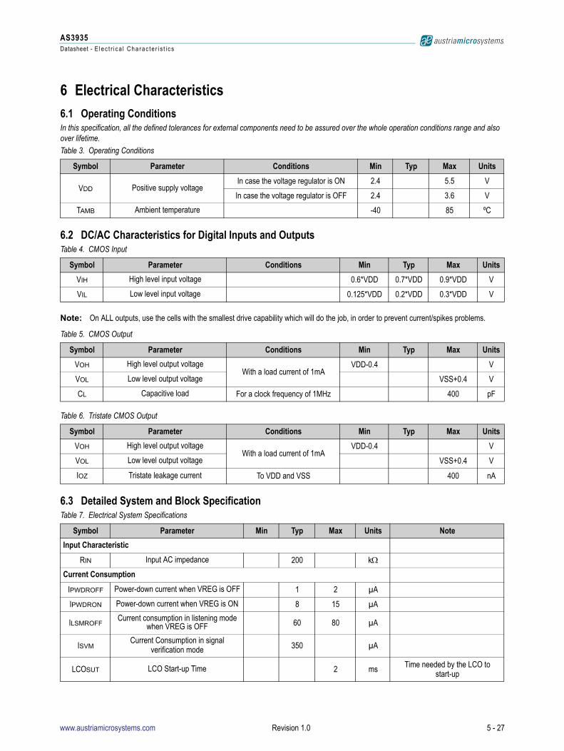
6 Electrical Characteristics
6.1 Operating ConditionsIn this specification, all the defined tolerances for external components need to be assured over the whole operation conditions range and also over lifetime.
6.2 DC/AC Characteristics for Digital Inputs and Outputs
Note: On ALL outputs, use the cells with the smallest drive capability which will do the job, in order to prevent current/spikes problems.
6.3 Detailed System and Block Specification
Table 3. Operating Conditions
Symbol Parameter Conditions Min Typ Max Units
VDD Positive supply voltageIn case the voltage regulator is ON 2.4 5.5 V
In case the voltage regulator is OFF 2.4 3.6 V
TAMB Ambient temperature -40 85 ºC
Table 4. CMOS Input
Symbol Parameter Conditions Min Typ Max Units
VIH High level input voltage 0.6*VDD 0.7*VDD 0.9*VDD V
VIL Low level input voltage 0.125*VDD 0.2*VDD 0.3*VDD V
Table 5. CMOS Output
Symbol Parameter Conditions Min Typ Max Units
VOH High level output voltageWith a load current of 1mA
VDD-0.4 V
VOL Low level output voltage VSS+0.4 V
CL Capacitive load For a clock frequency of 1MHz 400 pF
Table 6. Tristate CMOS Output
Symbol Parameter Conditions Min Typ Max Units
VOH High level output voltageWith a load current of 1mA
VDD-0.4 V
VOL Low level output voltage VSS+0.4 V
IOZ Tristate leakage current To VDD and VSS 400 nA
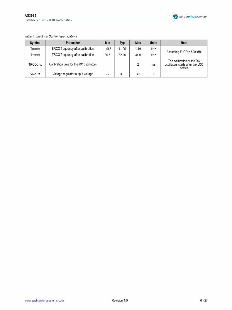
Table 7. Electrical System Specifications
Symbol Parameter Min Typ Max Units Note
Input Characteristic
RIN Input AC impedance 200 k
Current Consumption
IPWDROFF Power-down current when VREG is OFF 1 2 µA
IPWDRON Power-down current when VREG is ON 8 15 µA
ILSMROFF Current consumption in listening mode when VREG is OFF 60 80 µA
ISVMCurrent Consumption in signal
verification mode 350 µA
LCOSUT LCO Start-up Time 2 ms Time needed by the LCO to start-up
www.austriamicrosystems.com Revision 1.0 5 - 27
AS3935Datasheet - E l e c t r i c a l C h a r a c t e r i s t i c s
TSRCO SRCO frequency after calibration 1.065 1.125 1.19 kHzAssuming FLCO = 500 kHz
TTRCO TRCO frequency after calibration 30.5 32.26 34.0 kHz
TRCOCAL Calibration time for the RC oscillators 2 msThe calibration of the RC
oscillators starts after the LCO settles
VROUT Voltage regulator output voltage 2.7 3.0 3.3 V
Table 7. Electrical System Specifications
Symbol Parameter Min Typ Max Units Note
www.austriamicrosystems.com Revision 1.0 6 - 27
AS3935Datasheet - Ty p i c a l O p e r a t i n g C h a r a c t e r i s t i c s
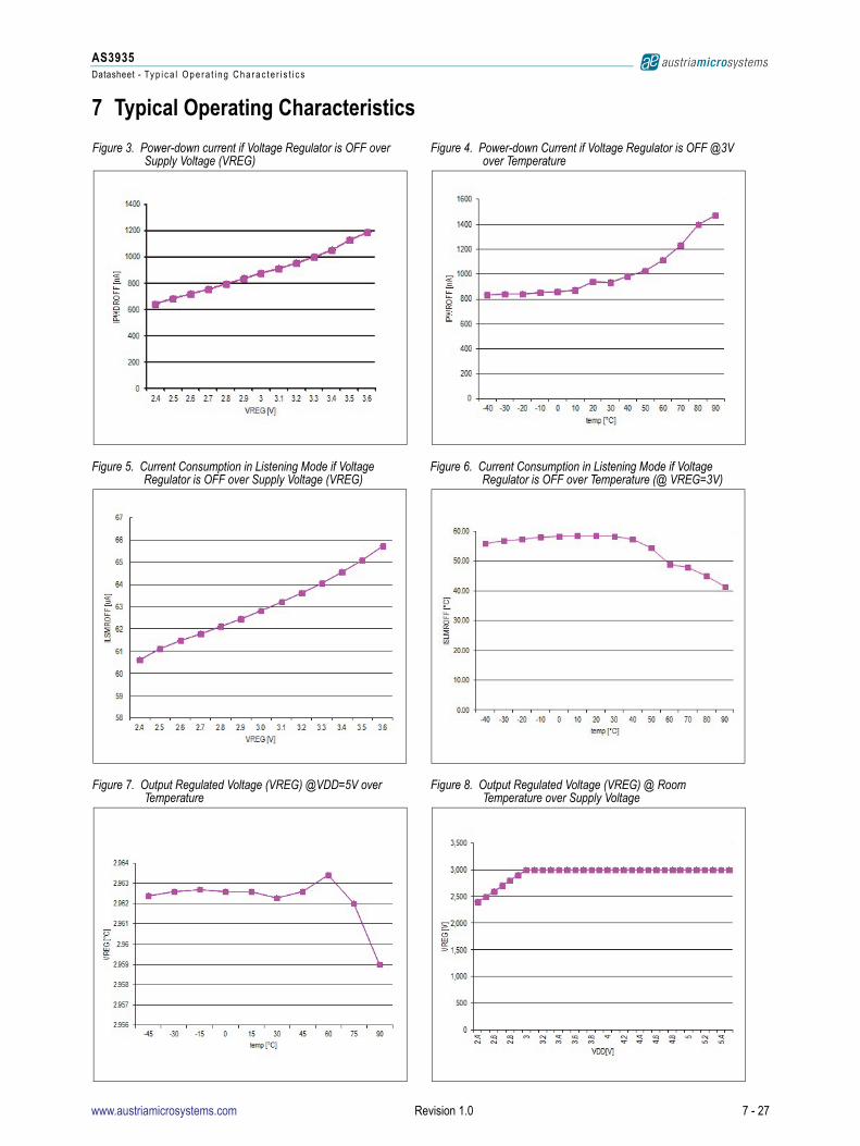
7 Typical Operating Characteristics
Figure 3. Power-down current if Voltage Regulator is OFF over Supply Voltage (VREG)
Figure 4. Power-down Current if Voltage Regulator is OFF @3V over Temperature
Figure 5. Current Consumption in Listening Mode if Voltage Regulator is OFF over Supply Voltage (VREG)
Figure 6. Current Consumption in Listening Mode if Voltage Regulator is OFF over Temperature (@ VREG=3V)
Figure 7. Output Regulated Voltage (VREG) @VDD=5V over Temperature
Figure 8. Output Regulated Voltage (VREG) @ Room Temperature over Supply Voltage
www.austriamicrosystems.com Revision 1.0 7 - 27
AS3935Datasheet - D e t a i l e d D e s c r i p t i o n
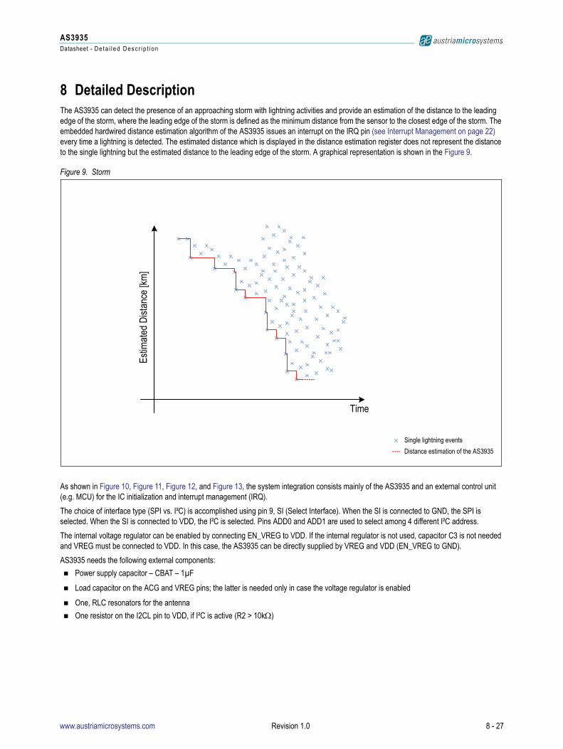
8 Detailed DescriptionThe AS3935 can detect the presence of an approaching storm with lightning activities and provide an estimation of the distance to the leading edge of the storm, where the leading edge of the storm is defined as the minimum distance from the sensor to the closest edge of the storm. The embedded hardwired distance estimation algorithm of the AS3935 issues an interrupt on the IRQ pin (see Interrupt Management on page 22) every time a lightning is detected. The estimated distance which is displayed in the distance estimation register does not represent the distance to the single lightning but the estimated distance to the leading edge of the storm. A graphical representation is shown in the Figure 9.
Figure 9. Storm
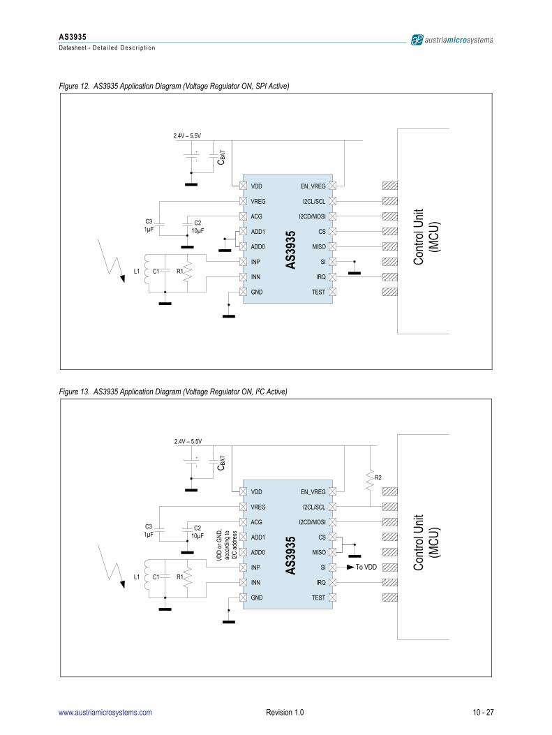
As shown in Figure 10, Figure 11, Figure 12, and Figure 13, the system integration consists mainly of the AS3935 and an external control unit (e.g. MCU) for the IC initialization and interrupt management (IRQ).
The choice of interface type (SPI vs. I²C) is accomplished using pin 9, SI (Select Interface). When the SI is connected to GND, the SPI is selected. When the SI is connected to VDD, the I²C is selected. Pins ADD0 and ADD1 are used to select among 4 different I²C address.
The internal voltage regulator can be enabled by connecting EN_VREG to VDD. If the internal regulator is not used, capacitor C3 is not needed and VREG must be connected to VDD. In this case, the AS3935 can be directly supplied by VREG and VDD (EN_VREG to GND).
AS3935 needs the following external components:
Power supply capacitor – CBAT – 1µF
Load capacitor on the ACG and VREG pins; the latter is needed only in case the voltage regulator is enabled
One, RLC resonators for the antenna
One resistor on the I2CL pin to VDD, if I²C is active (R2 > 10k)
Estim
ated
Dis
tanc
e [k
m]
Time
Single lightning events
Distance estimation of the AS3935
www.austriamicrosystems.com Revision 1.0 8 - 27

AS3935Datasheet - D e t a i l e d D e s c r i p t i o n
Figure 10. AS3935 Application Diagram (Voltage Regulator OFF, SPI Active)
Figure 11. AS3935 Application Diagram (Voltage Regulator OFF, I²C Active)
R1C1L1
EN_VREG
I2CL/SCL
INP
ACG
VREG
INN
ADD1
ADD0
GND
VDD
TEST
SI
IRQ
MISO
CS
I2CD/MOSI
AS3
935
CBA
T
Con
trol U
nit
(MC
U)
2.4V - 3.6V
C210µF
R1C1L1
EN_VREG
I2CL/SCL
INP
ACG
VREG
INN
ADD1
ADD0
GND
VDD
TEST
SI
IRQ
MISO
CS
I2CD/MOSI
AS3
935
CBA
T
Con
trol U
nit
(MC
U)
To VDD
R2
VDD
or G
ND
, ac
cord
ing
to
I2C
add
ress
2.4V - 3.6V
C210µF
www.austriamicrosystems.com Revision 1.0 9 - 27
AS3935Datasheet - D e t a i l e d D e s c r i p t i o n
Figure 12. AS3935 Application Diagram (Voltage Regulator ON, SPI Active)
Figure 13. AS3935 Application Diagram (Voltage Regulator ON, I²C Active)
R1C1L1
EN_VREG
I2CL/SCL
INP
ACG
VREG
INN
ADD1
ADD0
GND
VDD
TEST
SI
IRQ
MISO
CS
I2CD/MOSI
AS3
935
CBA
T
Con
trol U
nit
(MC
U)
2.4V – 5.5V
C210µF
C31µF
C210µF
R1C1L1
EN_VREG
I2CL/SCL
INP
ACG
VREG
INN
ADD1
ADD0
GND
VDD
TEST
SI
IRQ
MISO
CS
I2CD/MOSI
AS3
935
CBA
T
Con
trol U
nit
(MC
U)
To VDD
R2
VDD
or G
ND
, ac
cord
ing
to
I2C
add
ress
2.4V – 5.5V
C31µF
www.austriamicrosystems.com Revision 1.0 10 - 27
AS3935Datasheet - D e t a i l e d D e s c r i p t i o n
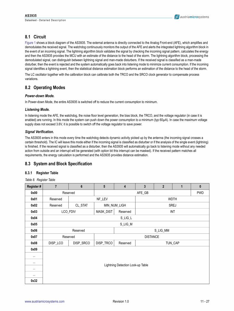
8.1 CircuitFigure 1 shows a block diagram of the AS3935. The external antenna is directly connected to the Analog Front-end (AFE), which amplifies and demodulates the received signal. The watchdog continuously monitors the output of the AFE and alerts the integrated lightning algorithm block in the event of an incoming signal. The lightning algorithm block validates the signal by checking the incoming signal pattern, calculates the energy and then the AS3935 provides the MCU with an estimate of the distance to the head of the storm. The lightning algorithm block, processing the demodulated signal, can distinguish between lightning signal and man-made disturbers. If the received signal is classified as a man-made disturber, then the event is rejected and the system automatically goes back into listening mode to minimize current consumption. If the incoming signal identifies a lightning event, then the statistical distance estimation block performs an estimation of the distance to the head of the storm.
The LC oscillator together with the calibration block can calibrate both the TRCO and the SRCO clock generator to compensate process variations.
8.2 Operating Modes
Power-down Mode.
In Power-down Mode, the entire AS3935 is switched off to reduce the current consumption to minimum.
Listening Mode.
In listening mode the AFE, the watchdog, the noise floor level generation, the bias block, the TRCO, and the voltage regulator (in case it is enabled) are running. In this mode the system can push down the power consumption to a minimum (typ 60µA). In case the maximum voltage supply does not exceed 3.6V, it is possible to switch off the voltage regulator to save power.
Signal Verification.
The AS3935 enters in this mode every time the watchdog detects dynamic activity picked up by the antenna (the incoming signal crosses a certain threshold). The IC will leave this mode either if the incoming signal is classified as disturber or if the analysis of the single event (lightning) is finished. If the received signal is classified as a disturber, then the AS3935 will automatically go back to listening mode without any needed action from outside and an interrupt will be generated (with option bit this interrupt can be masked). If the received pattern matches all requirements, the energy calculation is performed and the AS3935 provides distance estimation.
8.3 System and Block Specification
8.3.1 Register Table
Table 8. Register Table
Register # 7 6 5 4 3 2 1 0
0x00 Reserved AFE_GB PWD
0x01 Reserved NF_LEV WDTH
0x02 Reserved CL_STAT MIN_NUM_LIGH SREJ
0x03 LCO_FDIV MASK_DIST Reserved INT
0x04 S_LIG_L
0x05 S_LIG_M
0x06 Reserved S_LIG_MM
0x07 Reserved DISTANCE
0x08 DISP_LCO DISP_SRCO DISP_TRCO Reserved TUN_CAP
0x09
Lightning Detection Look-up Table
...
...
...
...
0x32
www.austriamicrosystems.com Revision 1.0 11 - 27
AS3935Datasheet - D e t a i l e d D e s c r i p t i o n
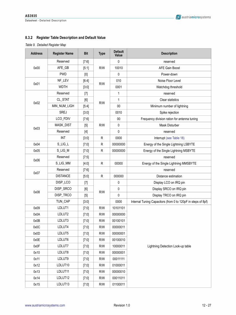
8.3.2 Register Table Description and Default Value
Table 9. Detailed Register Map
Address Register Name Bit Type Default Value Description
0x00
Reserved [7:6]
R/W
0 reserved
AFE_GB [5:1] 10010 AFE Gain Boost
PWD [0] 0 Power-down
0x01NF_LEV [6:4]
R/W010 Noise Floor Level
WDTH [3:0] 0001 Watchdog threshold
0x02
Reserved [7]
R/W
1 reserved
CL_STAT [6] 1 Clear statistics
MIN_NUM_LIGH [5:4] 00 Minimum number of lightning
SREJ [3:0] 0010 Spike rejection
0x03
LCO_FDIV [7:6]
R/W
00 Frequency division ration for antenna tuning
MASK_DIST [5] 0 Mask Disturber
Reserved [4] 0 reserved
INT [3:0] R 0000 Interrupt (see Table 18)
0x04 S_LIG_L [7:0] R 00000000 Energy of the Single Lightning LSBYTE
0x05 S_LIG_M [7:0] R 00000000 Energy of the Single Lightning MSBYTE
0x06Reserved [7:5] reserved
S_LIG_MM [4:0] R 00000 Energy of the Single Lightning MMSBYTE
0x07Reserved [7:6] reserved
DISTANCE [5:0] R 000000 Distance estimation
0x08
DISP_LCO [7]
R/W
0 Display LCO on IRQ pin
DISP_SRCO [6] 0 Display SRCO on IRQ pin
DISP_TRCO [5] 0 Display TRCO on IRQ pin
TUN_CAP [3:0] 0000 Internal Tuning Capacitors (from 0 to 120pF in steps of 8pf)
0x09 LDLUT1 [7:0] R/W 10101101
Lightning Detection Look-up table
0x0A LDLUT2 [7:0] R/W 00000000
0x0B LDLUT3 [7:0] R/W 00100101
0x0C LDLUT4 [7:0] R/W 00000011
0x0D LDLUT5 [7:0] R/W 00000001
0x0E LDLUT6 [7:0] R/W 00100010
0x0F LDLUT7 [7:0] R/W 10000011
0x10 LDLUT8 [7:0] R/W 00000001
0x11 LDLUT9 [7:0] R/W 00011111
0x12 LDLUT10 [7:0] R/W 01000011
0x13 LDLUT11 [7:0] R/W 00000010
0x14 LDLUT12 [7:0] R/W 00011011
0x15 LDLUT13 [7:0] R/W 01100011
www.austriamicrosystems.com Revision 1.0 12 - 27
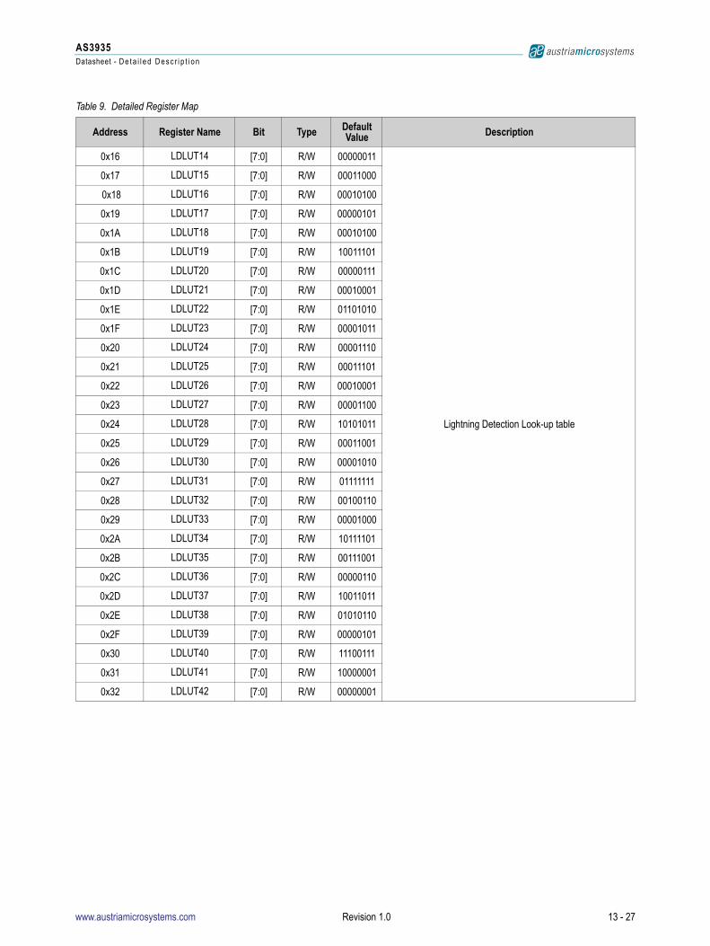
AS3935Datasheet - D e t a i l e d D e s c r i p t i o n
0x16 LDLUT14 [7:0] R/W 00000011
Lightning Detection Look-up table
0x17 LDLUT15 [7:0] R/W 00011000
0x18 LDLUT16 [7:0] R/W 00010100
0x19 LDLUT17 [7:0] R/W 00000101
0x1A LDLUT18 [7:0] R/W 00010100
0x1B LDLUT19 [7:0] R/W 10011101
0x1C LDLUT20 [7:0] R/W 00000111
0x1D LDLUT21 [7:0] R/W 00010001
0x1E LDLUT22 [7:0] R/W 01101010
0x1F LDLUT23 [7:0] R/W 00001011
0x20 LDLUT24 [7:0] R/W 00001110
0x21 LDLUT25 [7:0] R/W 00011101
0x22 LDLUT26 [7:0] R/W 00010001
0x23 LDLUT27 [7:0] R/W 00001100
0x24 LDLUT28 [7:0] R/W 10101011
0x25 LDLUT29 [7:0] R/W 00011001
0x26 LDLUT30 [7:0] R/W 00001010
0x27 LDLUT31 [7:0] R/W 01111111
0x28 LDLUT32 [7:0] R/W 00100110
0x29 LDLUT33 [7:0] R/W 00001000
0x2A LDLUT34 [7:0] R/W 10111101
0x2B LDLUT35 [7:0] R/W 00111001
0x2C LDLUT36 [7:0] R/W 00000110
0x2D LDLUT37 [7:0] R/W 10011011
0x2E LDLUT38 [7:0] R/W 01010110
0x2F LDLUT39 [7:0] R/W 00000101
0x30 LDLUT40 [7:0] R/W 11100111
0x31 LDLUT41 [7:0] R/W 10000001
0x32 LDLUT42 [7:0] R/W 00000001
Table 9. Detailed Register Map
Address Register Name Bit Type Default Value Description
www.austriamicrosystems.com Revision 1.0 13 - 27
AS3935Datasheet - D e t a i l e d D e s c r i p t i o n
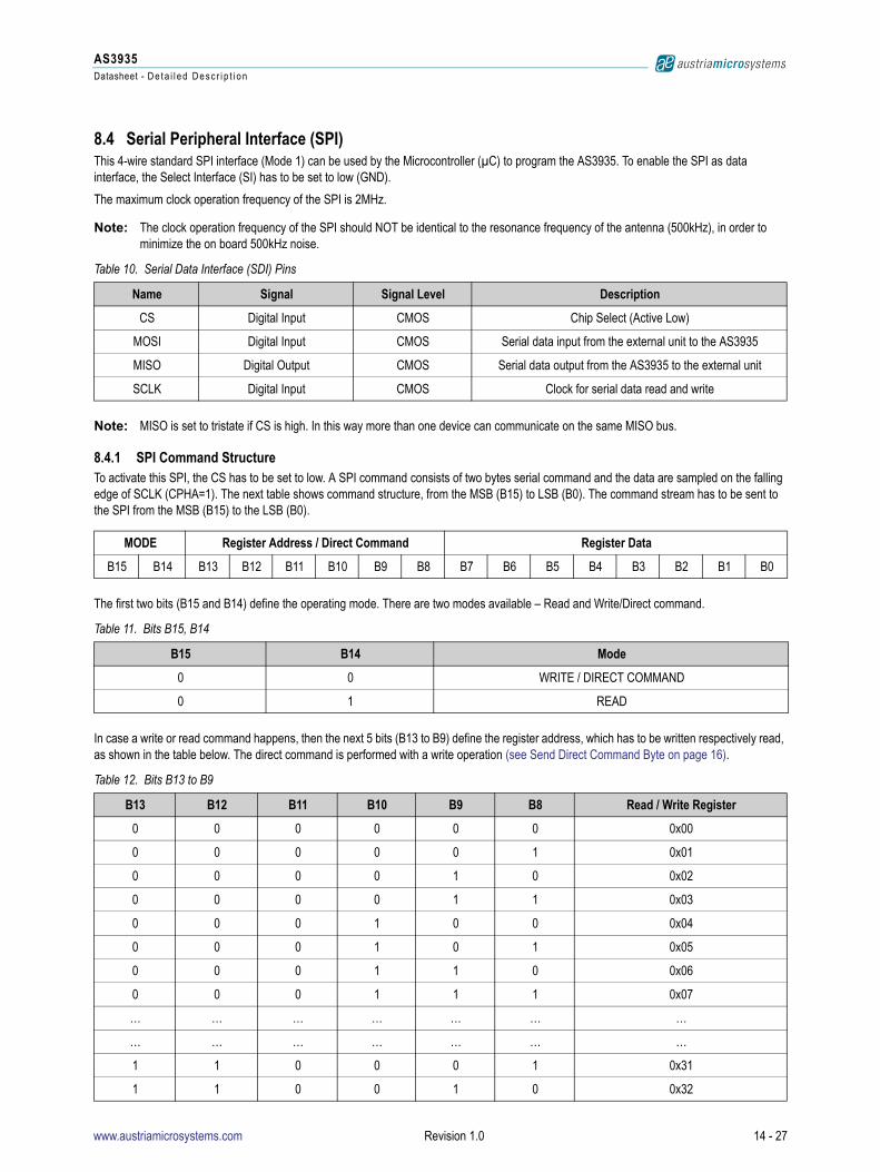
8.4 Serial Peripheral Interface (SPI)This 4-wire standard SPI interface (Mode 1) can be used by the Microcontroller (µC) to program the AS3935. To enable the SPI as data interface, the Select Interface (SI) has to be set to low (GND).
The maximum clock operation frequency of the SPI is 2MHz.
Note: The clock operation frequency of the SPI should NOT be identical to the resonance frequency of the antenna (500kHz), in order to minimize the on board 500kHz noise.
Note: MISO is set to tristate if CS is high. In this way more than one device can communicate on the same MISO bus.
8.4.1 SPI Command StructureTo activate this SPI, the CS has to be set to low. A SPI command consists of two bytes serial command and the data are sampled on the falling edge of SCLK (CPHA=1). The next table shows command structure, from the MSB (B15) to LSB (B0). The command stream has to be sent to the SPI from the MSB (B15) to the LSB (B0).
The first two bits (B15 and B14) define the operating mode. There are two modes available – Read and Write/Direct command.
In case a write or read command happens, then the next 5 bits (B13 to B9) define the register address, which has to be written respectively read, as shown in the table below. The direct command is performed with a write operation (see Send Direct Command Byte on page 16).
Table 10. Serial Data Interface (SDI) Pins
Name Signal Signal Level Description
CS Digital Input CMOS Chip Select (Active Low)
MOSI Digital Input CMOS Serial data input from the external unit to the AS3935
MISO Digital Output CMOS Serial data output from the AS3935 to the external unit
SCLK Digital Input CMOS Clock for serial data read and write
MODE Register Address / Direct Command Register Data
B15 B14 B13 B12 B11 B10 B9 B8 B7 B6 B5 B4 B3 B2 B1 B0
Table 11. Bits B15, B14
B15 B14 Mode
0 0 WRITE / DIRECT COMMAND
0 1 READ
Table 12. Bits B13 to B9
B13 B12 B11 B10 B9 B8 Read / Write Register
0 0 0 0 0 0 0x00
0 0 0 0 0 1 0x01
0 0 0 0 1 0 0x02
0 0 0 0 1 1 0x03
0 0 0 1 0 0 0x04
0 0 0 1 0 1 0x05
0 0 0 1 1 0 0x06
0 0 0 1 1 1 0x07
… … … … … … …
… … … … … … …
1 1 0 0 0 1 0x31
1 1 0 0 1 0 0x32
www.austriamicrosystems.com Revision 1.0 14 - 27
AS3935Datasheet - D e t a i l e d D e s c r i p t i o n
8.4.2 Writing of Register Data
Figure 14. SPI Page Write
8.4.3 Reading of Data from Addressable Registers (READ Mode)Once the address has been sent via SPI, the data can be fed through the MISO pin out to the microcontroller.
A CS high toggling high-low-high has to be performed after finishing the read mode session, in order to indicate the end of the READ command and prepare the Interface to the next command control Byte.
To transfer bytes from consecutive addresses, SPI master has to keep the CS signal low and the SCLK clock has to be active as long as data need to be read.
Figure 15. SPI Read Byte
CS
SCLK
MOSI 0 0 A5
A4
A3
A2
A1
A0
D5
D4
D3
D2
D1
D0
D7
D6
XX D5
D4
D3
D2
D1
D0
D7
D6
D7
D6
D5
D4
D3
D2
D1
D0
D7
D6
D1
Two leading Zeros indicate WRITE Mode
Data is moved to Address <A5-A0 >
Data is moved to Address
<A5-A0 > + 1
Data is moved to Address
<A5-A0 > + (n-1)
Data is moved to Address
<A5-A0 > + n
CS falling edge signals end of WRITE Mode
D0
CS
SCLK
MOSI 0 1 A5 A4 A3 A2 A1 A0 XX
D4 D3 D2 D1 D0D7 D6 XXMISO D5
SCLK rising edge Data is transferred from µC
01 pattern indicates READ Mode
SCLK falling edge Data is sampled
SCLK rising edge Data is moved from Address <A5-A0>
SCLK falling edge Data is transferred to µC
CS falling edge signals end of READ Mode
www.austriamicrosystems.com Revision 1.0 15 - 27

AS3935Datasheet - D e t a i l e d D e s c r i p t i o n
8.4.4 Send Direct Command ByteIt is possible to send direct commands by writing 0x96 in the registers REG0x3C and REG0x3D, as shown in the table below:
8.5 I²CAn I²C slave interface is implemented for read/write access to the internal registers and to send direct commands. To enable the I²C as interface, the Select Interface pin has to be set to the positive voltage supply (SI=VDD). The I2CL is the clock bus, while the I2CD is the data bus. An external pull-up resistor on the I2CL pin is needed.
The device addresses for the AS3935 in read or write mode are defined by:
0-0-0-0-0-a1-a0-0: write mode device address (DW)
0-0-0-0-0-a1-a0-1: read mode device address (DR)
Where a0 and a1 are defined by the pins 5 (ADD0) and 6 (ADD1).
Figure 16. I²C Timing Diagram
Table 13. Registers 0x3C, 0x3D
Direct Command Register Description
PRESET_DEFAULT 0x3C Sets all registers in default mode
CALIB_RCO 0x3D Calibrates automatically the internal RC Oscillators
Table 14. I²C Parameters
Symbol Parameter Conditions Min Typ Max Units
TSP Spike intensity 50 100 ns
THI High Clock Time400 kHz Clock speed
330 ns
TLO Low Clock Time 660 ns
TSU I2CD has to change Tsetup before rising edge I2CL 30 ns
THD No hold time needed for I2CD relative to rising edge of I2CL -40 ns
THD;STA Within start condition, after low going I2CD, I2CL has to stay constant for specified hold time 300 ns
TSU;STO After high going edge of I2CL, I2CD has to stay constant for the specified setup time before STOP or repeated start condition is applied
100 ns
TSU;STA 100 ns
I2CD
I2CL
start
THD;STA
TLO
THI
TF
TSU;DAT
sr
TSU;STA
TSPTSU;STO
stop
TR
www.austriamicrosystems.com Revision 1.0 16 - 27
AS3935Datasheet - D e t a i l e d D e s c r i p t i o n
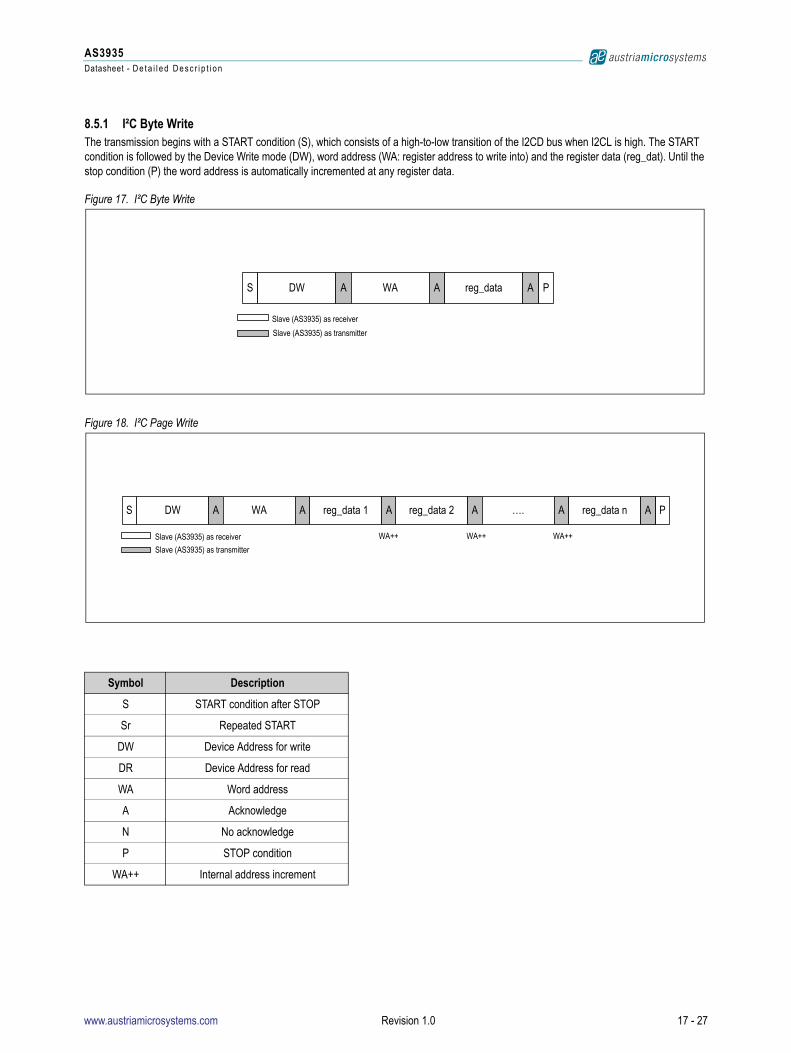
8.5.1 I²C Byte WriteThe transmission begins with a START condition (S), which consists of a high-to-low transition of the I2CD bus when I2CL is high. The START condition is followed by the Device Write mode (DW), word address (WA: register address to write into) and the register data (reg_dat). Until the stop condition (P) the word address is automatically incremented at any register data.
Figure 17. I²C Byte Write
Figure 18. I²C Page Write
Symbol Description
S START condition after STOP
Sr Repeated START
DW Device Address for write
DR Device Address for read
WA Word address
A Acknowledge
N No acknowledge
P STOP condition
WA++ Internal address increment
S DW A WA A reg_data PA
Slave (AS3935) as receiver
Slave (AS3935) as transmitter
S DW A WA A reg_data 1 PA reg_data Areg_data Areg_data 2 A …. A reg_data n AAA
WA++ WA++ WA++Slave (AS3935) as receiver
Slave (AS3935) as transmitter
www.austriamicrosystems.com Revision 1.0 17 - 27
AS3935Datasheet - D e t a i l e d D e s c r i p t i o n
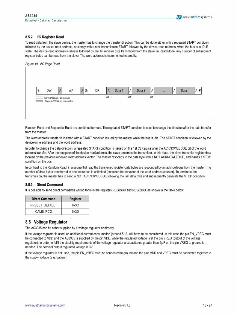
8.5.2 I²C Register ReadTo read data from the slave device, the master has to change the transfer direction. This can be done either with a repeated START condition followed by the device-read address, or simply with a new transmission START followed by the device-read address, when the bus is in IDLE state. The device-read address is always followed by the 1st register byte transmitted from the slave. In Read Mode, any number of subsequent register bytes can be read from the slave. The word address is incremented internally.
Figure 19. I²C Page Read
Random Read and Sequential Read are combined formats. The repeated START condition is used to change the direction after the data transfer from the master.
The word address transfer is initiated with a START condition issued by the master while the bus is idle. The START condition is followed by the device-write address and the word address.
In order to change the data direction, a repeated START condition is issued on the 1st CLK pulse after the ACKNOWLEDGE bit of the word address transfer. After the reception of the device-read address, the slave becomes the transmitter. In this state, the slave transmits register data located by the previous received word address vector. The master responds to the data byte with a NOT ACKNOWLEDGE, and issues a STOP condition on the bus.
In contrast to the Random Read, in a sequential read the transferred register-data bytes are responded by an acknowledge from the master. The number of data bytes transferred in one sequence is unlimited (consider the behavior of the word-address counter). To terminate the transmission, the master has to send a NOT ACKNOWLEDGE following the last data byte and subsequently generate the STOP condition.
8.5.3 Direct CommandIt is possible to send direct commands writing 0x96 in the registers REG0x3C and REG0x3D, as shown in the table below:
8.6 Voltage RegulatorThe AS3935 can be either supplied by a voltage regulator or directly.
If the voltage regulator is used, an additional current consumption (around 5µA) will have to be considered. In this case the pin EN_VREG must be connected to VDD and the AS3935 is supplied by the pin VDD, while the regulated voltage is at the pin VREG (output of the voltage regulator). In order to fulfil the stability requirements of the voltage regulator a capacitance greater than 1µF on the pin VREG to ground is needed. The nominal output regulated voltage is 3V.
If the voltage regulator is not used, the pin EN_VREG must be connected to ground and the pins VDD and VREG must be connected together to the supply voltage (e.g. battery).
Direct Command Register
PRESET_DEFAULT 0x3C
CALIB_RCO 0x3D
S DW A WA A DR PA Data 1 AAA Data 2 A …... A
WA++ WA++ WA++
Sr Data n A
Slave (AS3935) as transmitterSlave (AS3935) as receiver
www.austriamicrosystems.com Revision 1.0 18 - 27
AS3935Datasheet - D e t a i l e d D e s c r i p t i o n
8.7 Analog Front-end (AFE) and WatchdogThe AFE amplifies and demodulates the AC-signal picked up by the antenna. Since the AS3935 is a lightning sensor based on narrowband receiving technique, the AFE bandwidth is meant to be greater than the antenna bandwidth. In this way, it is possible to consider that the gain within the antenna bandwidth as constant.
The gain of the AFE by default is optimized to operate indoor (e.g. inside a building). If the AS3935 operates outdoor, then the AFE gain setting has to be set to a lower value, as shown in the Table 15.
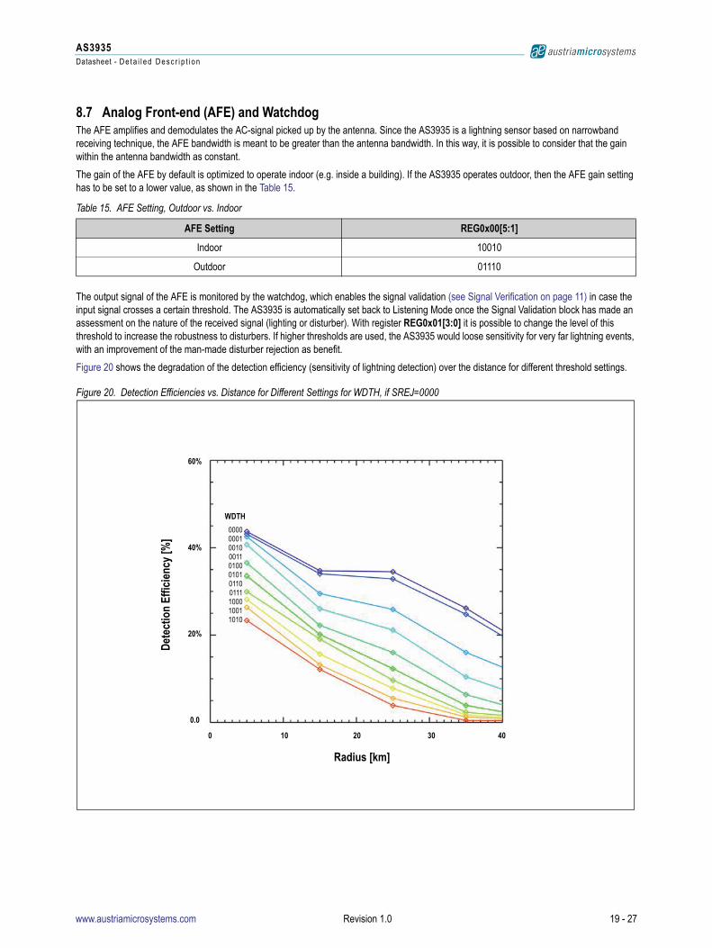
The output signal of the AFE is monitored by the watchdog, which enables the signal validation (see Signal Verification on page 11) in case the input signal crosses a certain threshold. The AS3935 is automatically set back to Listening Mode once the Signal Validation block has made an assessment on the nature of the received signal (lighting or disturber). With register REG0x01[3:0] it is possible to change the level of this threshold to increase the robustness to disturbers. If higher thresholds are used, the AS3935 would loose sensitivity for very far lightning events, with an improvement of the man-made disturber rejection as benefit.
Figure 20 shows the degradation of the detection efficiency (sensitivity of lightning detection) over the distance for different threshold settings.
Figure 20. Detection Efficiencies vs. Distance for Different Settings for WDTH, if SREJ=0000
Table 15. AFE Setting, Outdoor vs. Indoor
AFE Setting REG0x00[5:1]
Indoor 10010
Outdoor 01110
60%
40%
20%
0.0
0 10 20 30 40
Det
ectio
n Ef
ficie
ncy
[%]
00000001001000110100010101100111100010011010
Radius [km]
WDTH
www.austriamicrosystems.com Revision 1.0 19 - 27
AS3935Datasheet - D e t a i l e d D e s c r i p t i o n
8.8 Noise Floor Generator and EvaluationThe output signal of the AFE is also used to generate the noise floor level. The noise floor is continuously compared to a reference voltage (noise threshold). Whenever the noise floor level crosses the noise threshold, the AS3935 issues an interrupt (INT_NH) to inform the external unit (e.g. MCU) that the AS3935 cannot operate properly due to the high input noise received by the antenna (e.g. blocker). It is possible to set the threshold for the noise floor limit with the bits REG0x01[6:4], as defined in the table below.
INT_NH is displayed as long as the input noise level (blocker) is higher than the noise floor threshold. By default the setting REG0x01[6:4] =010 is used.
8.9 Lightning Algorithm The lightning algorithm consists of hardwired logic. False events (man-made disturbers) which might trigger the AS3935 are rejected, while lightning events initiate calculations to estimate the distance to the head of the storm.
The Lightning algorithm is broken up into three sub blocks:
1. Signal validation: Verification that the incoming signal can be classified as lightning.
2. Energy calculation: Calculation of the energy of the single event.
3. Statistical distance estimation: According to the number of stored events (lightning), a distance estimate is calculated.
If the signal validation fails (the incoming signal does not have the characteristics of lightning), the energy calculation and statistical distance estimation do not happen and the event is classified as disturber.
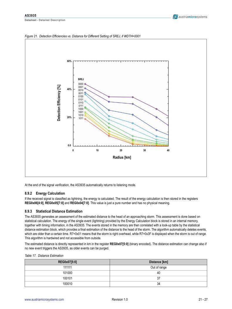
8.9.1 Signal ValidationThe watchdog enables the lightning algorithm block in the event any activities are detected at the antenna. As this happens the output signal of the AFE is evaluated by the Signal Validation block, which checks the pattern of the received signal. The signal validation checks the shape of the received signal. In particular, the AS3935 can reject the impulse signals, like spikes, picked up by the antenna. The AS3935 has the ability to improve the spike rejection with the register REG0x02[3:0]. By default, register REG0x02[3:0] =0010. Larger values in REG0x02[3:0] correspond to more robust disturber rejection, with a decrease of the detection efficiency, as shown in the Figure 21.
Table 16. Settings for the Noise Floor Threshold
Continuous Input Noise Level[µVrms] (outdoor)
Continuous Input Noise Level [µVrms] (indoor) REG0x01[6] REG0x01[5] REG0x01[4]
390 28 0 0 0
630 45 0 0 1
860 62 0 1 0
1100 78 0 1 1
1140 95 1 0 0
1570 112 1 0 1
1800 130 1 1 0
2000 146 1 1 1
www.austriamicrosystems.com Revision 1.0 20 - 27
AS3935Datasheet - D e t a i l e d D e s c r i p t i o n
Figure 21. Detection Efficiencies vs. Distance for Different Setting of SREJ, if WDTH=0001
At the end of the signal verification, the AS3935 automatically returns to listening mode.
8.9.2 Energy CalculationIf the received signal is classified as lightning, the energy is calculated. The result of the energy calculation is then stored in the registers REG0x06[4:0], REG0x05[7:0] and REG0x04[7:0]. This value is just a pure number and has no physical meaning.
8.9.3 Statistical Distance EstimationThe AS3935 generates an assessment of the estimated distance to the head of an approaching storm. This assessment is done based on statistical calculation. The energy of the single event (lightning) provided by the Energy Calculation block is stored in an internal memory, together with timing information, in the AS3935. The events stored in the memory are then correlated with a look-up table by the statistical distance estimation block, which provides a final estimation of the distance to the head of the storm. The algorithm automatically deletes events, which are older than a certain time. R7=0x01 means that the storm is right overhead, while R7=0x3F is displayed when the storm is out of range. This algorithm is hardwired and not accessible from outside.
The estimated distance is directly represented in km in the register REG0x07[5:0] (binary encoded). The distance estimation can change also if no new event triggers the AS3935, as older events can be purged.
Table 17. Distance Estimation
REG0x07[5:0] Distance [km]
111111 Out of range
101000 40
100101 37
100010 34
60%
40%
20%
0.0
0 10 20 30 40
Det
ectio
n Ef
ficie
ncy
[%] 0000
00010010001101000101011001111000100110101011
Radius [km]
SREJ
www.austriamicrosystems.com Revision 1.0 21 - 27
AS3935Datasheet - D e t a i l e d D e s c r i p t i o n
The calculated energy is stored in registers REG0x04[7:0], REG0x05[7:0] and REG0x06[4:0].
8.9.4 Interrupt ManagementWhenever events happen, the AS3935 pulls the IRQ high and displays the interrupt in the REG0x03[3:0]. Table 18 shows the interrupt register.
The INT_NH is issued if the received noise exceeds the maximum acceptable noise. INT_NH persists until the noise is again back to low.
In case the signal validation block assesses the received signal as disturber, the INT_D is displayed. It is possible to mask the disturber interrupts INT_D with MASK_DIST (REG0x03[5] =1).
If the MASK_DIST option is enabled, the signal on the pin IRQ never goes high if a disturber is detected.
The interrupt bus IRQ is set back to low whenever the interrupt register is read out.
The AS3935 issues a lightning interrupt (INT_L) if a new event is detected. All new events are stored in the internal memory and build up a lightning statistic used by the distance estimation algorithm. If the AS3935 issues an interrupt and the Interrupt register is REG0x03[3:0] =000 the distance estimation has changed due to purging of old events in the statistics, based on the lightning distance estimation algorithm.
Whenever an interrupt is issued, the external unit should wait 2ms before reading the Interrupt register.
In addition, it is possible to allow the AS3935 to issue lightning interrupts only if a minimum number of events (lightning) have been detected in the last 15 minutes. The minimum number of lightning events can be set with register REG0x02[5:4].
When this feature is utilized, a minimum number of events must occur to trigger a valid lightning event. This eliminates false triggers by man-made disturbers that may pass the validation algorithm. It is possible to clear the statistics built up by the lightning distance estimation algorithm block by just toggling the bit REG0x02[6] (high-low-high).
011111 31
011011 27
011000 24
010100 20
010001 17
001110 14
001100 12
001010 10
001000 8
000110 6
000101 5
000001 Storm is Overhead
Table 18. Interrupts
Interrupt Name REG0x03[3:0] Description
INT_NH 0001 Noise level too high
INT_D 0100 Disturber detected
INT_L 1000 Lightning interrupt
Table 19. Minimum Number of Lightning Detection
Minimum Number of Lightning REG0x02[5] REG0x02[4]
1 0 0
5 0 1
9 1 0
16 1 1
Table 17. Distance Estimation
REG0x07[5:0] Distance [km]
www.austriamicrosystems.com Revision 1.0 22 - 27
AS3935Datasheet - D e t a i l e d D e s c r i p t i o n
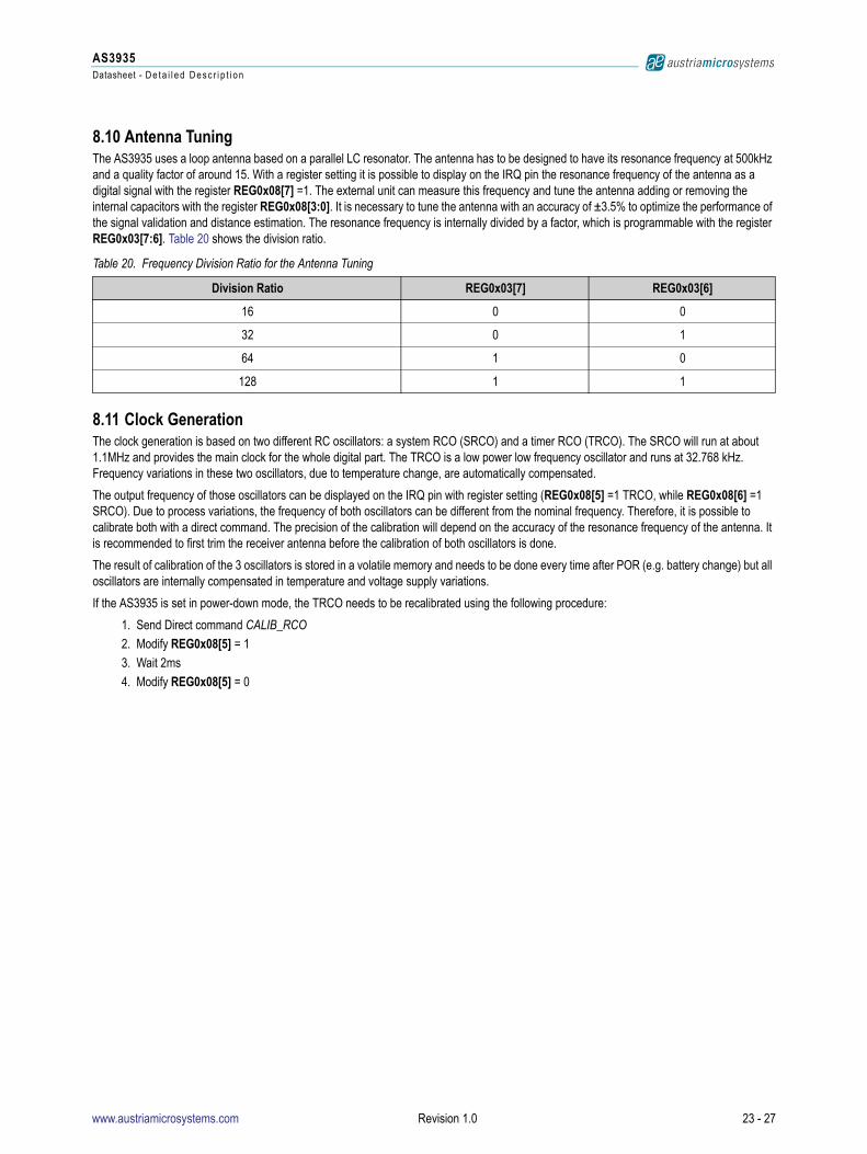
8.10 Antenna TuningThe AS3935 uses a loop antenna based on a parallel LC resonator. The antenna has to be designed to have its resonance frequency at 500kHz and a quality factor of around 15. With a register setting it is possible to display on the IRQ pin the resonance frequency of the antenna as a digital signal with the register REG0x08[7] =1. The external unit can measure this frequency and tune the antenna adding or removing the internal capacitors with the register REG0x08[3:0]. It is necessary to tune the antenna with an accuracy of ±3.5% to optimize the performance of the signal validation and distance estimation. The resonance frequency is internally divided by a factor, which is programmable with the register REG0x03[7:6]. Table 20 shows the division ratio.
8.11 Clock GenerationThe clock generation is based on two different RC oscillators: a system RCO (SRCO) and a timer RCO (TRCO). The SRCO will run at about 1.1MHz and provides the main clock for the whole digital part. The TRCO is a low power low frequency oscillator and runs at 32.768 kHz. Frequency variations in these two oscillators, due to temperature change, are automatically compensated.
The output frequency of those oscillators can be displayed on the IRQ pin with register setting (REG0x08[5] =1 TRCO, while REG0x08[6] =1 SRCO). Due to process variations, the frequency of both oscillators can be different from the nominal frequency. Therefore, it is possible to calibrate both with a direct command. The precision of the calibration will depend on the accuracy of the resonance frequency of the antenna. It is recommended to first trim the receiver antenna before the calibration of both oscillators is done.
The result of calibration of the 3 oscillators is stored in a volatile memory and needs to be done every time after POR (e.g. battery change) but all oscillators are internally compensated in temperature and voltage supply variations.
If the AS3935 is set in power-down mode, the TRCO needs to be recalibrated using the following procedure:
1. Send Direct command CALIB_RCO
2. Modify REG0x08[5] = 1
3. Wait 2ms
4. Modify REG0x08[5] = 0
Table 20. Frequency Division Ratio for the Antenna Tuning
Division Ratio REG0x03[7] REG0x03[6]
16 0 0
32 0 1
64 1 0
128 1 1
www.austriamicrosystems.com Revision 1.0 23 - 27
AS3935Datasheet - P a c k a g e D r a w i n g s a n d M a rk i n g s
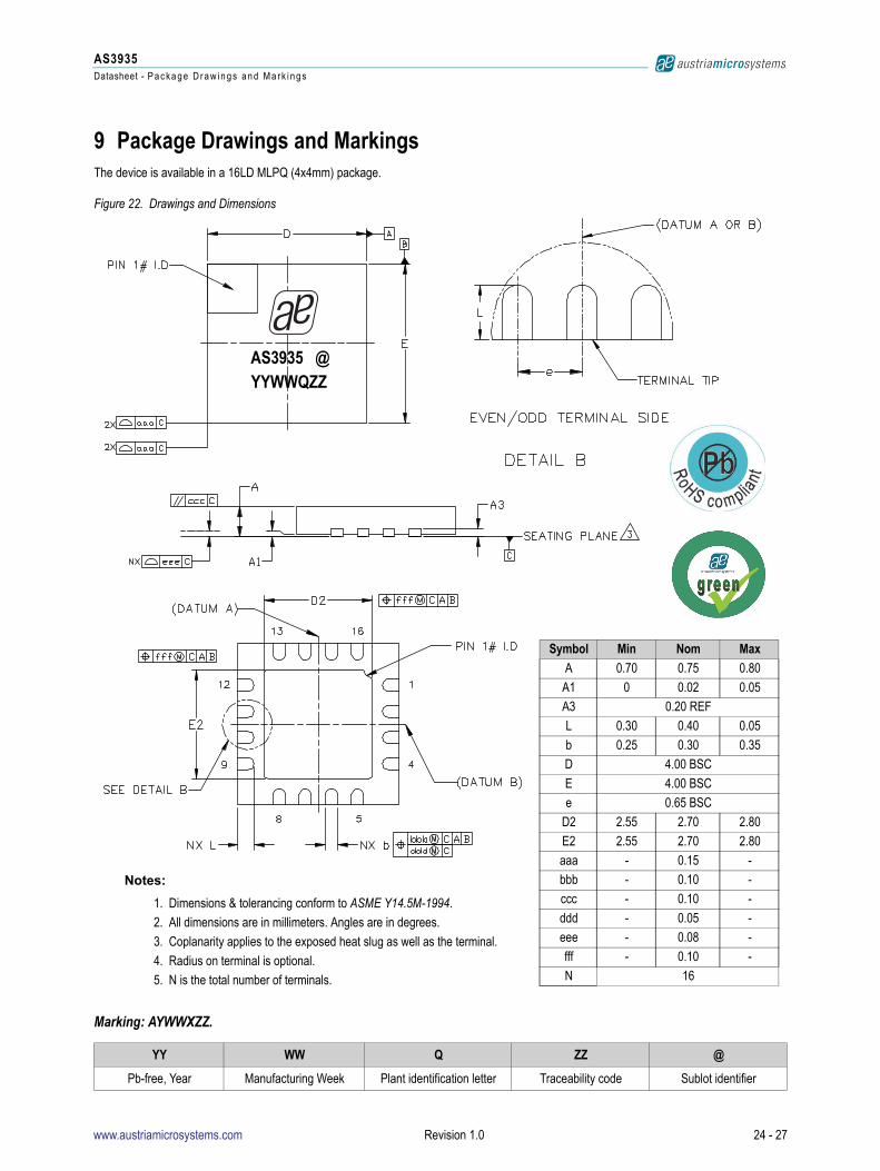
9 Package Drawings and MarkingsThe device is available in a 16LD MLPQ (4x4mm) package.
Figure 22. Drawings and Dimensions
Marking: AYWWXZZ.
YY WW Q ZZ @
Pb-free, Year Manufacturing Week Plant identification letter Traceability code Sublot identifier
AS3935 @YYWWQZZ
Symbol Min Nom Max
A 0.70 0.75 0.80
A1 0 0.02 0.05
A3 0.20 REF
L 0.30 0.40 0.05
b 0.25 0.30 0.35
D 4.00 BSC
E 4.00 BSC
e 0.65 BSC
D2 2.55 2.70 2.80
E2 2.55 2.70 2.80
aaa - 0.15 -
bbb - 0.10 -
ccc - 0.10 -
ddd - 0.05 -
eee - 0.08 -
fff - 0.10 -
N 16
Notes:
1. Dimensions & tolerancing conform to ASME Y14.5M-1994.
2. All dimensions are in millimeters. Angles are in degrees.
3. Coplanarity applies to the exposed heat slug as well as the terminal.
4. Radius on terminal is optional.
5. N is the total number of terminals.
www.austriamicrosystems.com Revision 1.0 24 - 27
AS3935Datasheet - R e v i s i o n H i s t o r y
Revision History
Note: Typos may not be explicitly mentioned under revision history.
Revision Date Owner Description
1.0 30 Apr, 2012 rlc Initial release
www.austriamicrosystems.com Revision 1.0 25 - 27
AS3935Datasheet - O r d e r i n g I n f o rm a t i o n
10 Ordering Information
Note: All products are RoHS compliant and austriamicrosystems green.Buy our products or get free samples online at ICdirect: http://www.austriamicrosystems.com/ICdirect
Technical Support is available at http://www.austriamicrosystems.com/Technical-Support
For further information and requests, please contact us mailto: [email protected] find your local distributor at http://www.austriamicrosystems.com/distributor
Table 21. Ordering Information
Ordering Code Package Type Marking Delivery Form Quantity
AS3935-BQFT MLPQ 4x4 16LD AS3935 7 inches Tape & Reel 1000 pcs
www.austriamicrosystems.com Revision 1.0 26 - 27
AS3935Datasheet - C o p y r i g h t s
Copyrights
Copyright © 1997-2012, austriamicrosystems AG, Tobelbaderstrasse 30, 8141 Unterpremstaetten, Austria-Europe. Trademarks Registered ®. All rights reserved. The material herein may not be reproduced, adapted, merged, translated, stored, or used without the prior written consent of the copyright owner.
All products and companies mentioned are trademarks or registered trademarks of their respective companies.
Disclaimer
Devices sold by austriamicrosystems AG are covered by the warranty and patent indemnification provisions appearing in its Term of Sale. austriamicrosystems AG makes no warranty, express, statutory, implied, or by description regarding the information set forth herein or regarding the freedom of the described devices from patent infringement. austriamicrosystems AG reserves the right to change specifications and prices at any time and without notice. Therefore, prior to designing this product into a system, it is necessary to check with austriamicrosystems AG for current information. This product is intended for use in normal commercial applications. Applications requiring extended temperature range, unusual environmental requirements, or high reliability applications, such as military, medical life-support or life-sustaining equipment are specifically not recommended without additional processing by austriamicrosystems AG for each application. For shipments of less than 100 parts the manufacturing flow might show deviations from the standard production flow, such as test flow or test location.
The information furnished here by austriamicrosystems AG is believed to be correct and accurate. However, austriamicrosystems AG shall not be liable to recipient or any third party for any damages, including but not limited to personal injury, property damage, loss of profits, loss of use, interruption of business or indirect, special, incidental or consequential damages, of any kind, in connection with or arising out of the furnishing, performance or use of the technical data herein. No obligation or liability to recipient or any third party shall arise or flow out of austriamicrosystems AG rendering of technical or other services.
This product is intended to be used as an early warning indicator for lightning related storms. It does not guarantee accuracy or predict exact strike locations. By using the part, the user shall be aware that s/he cannot just rely on the indication in order to prevent accidents caused by lightning strikes. austriamicrosystems explicitly states that the user must follow the generally known and recommended instructions on how to behave in the event of lightning strikes. In no event shall austriamicrosystems or its suppliers be liable for any direct, indirect, incidental, special, exemplary or consequential damages (including, but not limited to procurement of substitute goods or services, loss of use, data or profits, or business interruption) arising out of user’s disregard to such warnings and instructions.
Contact Information
Headquarters
austriamicrosystems AGTobelbaderstrasse 30A-8141 Unterpremstaetten, Austria
Tel: +43 (0) 3136 500 0Fax: +43 (0) 3136 525 01
For Sales Offices, Distributors and Representatives, please visit:
http://www.austriamicrosystems.com/contact
www.austriamicrosystems.com Revision 1.0 27 - 27


![tbd - OpenHacks · [v1-04] 2016-Jan-13 Document Feedback AS3935 − General Description Block Diagram The functional blocks of this device are shown below: Figure 2: AS3935 Block](https://img.pdfslide.us/doc/110x75/5e6d6753adc6cb7d4075a98a/tbd-openhacks-v1-04-2016-jan-13-document-feedback-as3935-a-general-description.jpg)