Embed Size (px)
Citation preview

HAL Id: hal-00905392https://hal.archives-ouvertes.fr/hal-00905392
Submitted on 18 Nov 2013
HAL is a multi-disciplinary open accessarchive for the deposit and dissemination of sci-entific research documents, whether they are pub-lished or not. The documents may come fromteaching and research institutions in France orabroad, or from public or private research centers.
L’archive ouverte pluridisciplinaire HAL, estdestinée au dépôt et à la diffusion de documentsscientifiques de niveau recherche, publiés ou non,émanant des établissements d’enseignement et derecherche français ou étrangers, des laboratoirespublics ou privés.
Modelling and engineering of stress based controlledoxidation effects for silicon nanostructures patterning
Xiang-Lei Han, Guilhem Larrieu, Christophe Krzeminski
To cite this version:Xiang-Lei Han, Guilhem Larrieu, Christophe Krzeminski. Modelling and engineering of stress basedcontrolled oxidation effects for silicon nanostructures patterning. Nanotechnology, Institute of Physics,2013, 24 (49), pp.495301. �hal-00905392�

Modelling and engineering of stress based controlled
oxidation effects for silicon nanostructures
patterning
Xiang-Lei Han
IEMN-UMR CNRS 8520, 59652 Villeneuve d’Ascq, France
Guilhem Larrieu
CNRS, LAAS, 7 avenue du colonel Roche, F-31400 Toulouse, France
Univ de Toulouse, LAAS, F-31400 Toulouse, France
E-mail: [email protected]
Christophe Krzeminski
IEMN-UMR CNRS 8520, Departement ISEN, 41 Boulevard Vauban, 59046 France
E-mail: [email protected]
Abstract. Silicon nanostructure patterning with a tight geometry control is an
important challenge at the bottom level. In that context, stress based controlled
oxidation appears as an efficient tools for precise nanofabrication. Here, we investigate
stress-retarded oxidation phenomenon in various silicon nanostructures (nanobeams,
nanorings and nanowires) both at the experimental and theoretical levels. Different
silicon nanostructures have been fabricated by a top-down approach. A complex
dependence of the stress build-up with the nanoobjects dimension, shape and size
have been demonstrated experimentally and physically explained by modelling. For
the oxidation of a two dimensional nanostructure (nanobeam), a relative independence
to size effects have been observed. On the other side, a radial stress increase with
geometry downscaling of one dimensional nanostructure (nanowire) have been carefully
emphasised. The study of the shape engineering by retarded oxidation effects for
vertical silicon nanowires is finally discussed.
Submitted to: Nanotechnology
2
1. Introduction
Self-limited [1, 2, 3, 4, 5] or retarded [6] oxidation in silicon nanostructures is an in-
teresting technological tool in order to manipulate the geometrical (the shape [7], the
size [8], the distribution [9]) or the physical properties [1, 10, 11] of silicon nano-objects.
Several applications have been foreseen using this effect such as a nano-field effect tran-
sistor [12], nanoflash memory [13, 14, 15]. However, the physical mechanisms underlying
remain poorly understood at the fundamental level and more knowledge is needed. The
computer simulation of such a processing is an identified issue. Atomistic simulations
are only able to describe the very first stage of the oxidation process [16, 17]. Large
concerns about the stress levels predicted at the atomistic scale of the Si/SiO2 interface
have been reported [18]. On the other hand, macroscopic simulations [19] fail to explain
these retarded or self-limited effects and cannot be used to predict the resulting shape
of the oxidised nanostructures [20]. This is a large concern for silicon based nanotech-
nology which should be addressed.
In this work, we present a large experimental and modelling study of the stress-
retarded oxidation effects and their influence in the nanostructure shape engineering.
Here, the seminal work of Kao et al. [21, 22] is revisited in various aspects, pointing out
the size effects in the oxidation of silicon nanostructures at the nanoscale level. First,
the orientation effects on simple planar bulk oxidation have been carefully investigated
in the experimental range. The influence of the surface shape (concave/convex) of the
nanoobject has been observed and quantified by the modelling of the oxidation kinetics.
For the nanobeam structure, the Finite Element Method (FEM) has been able to explain
the general shape of the oxidised structure but also the absence of retarded effect with
the scaling of the nanostructure width. Finally, size dependent self-limited oxidation
effects in silicon nanowires is reported and evaluated. Experimentally, the improvement
of the high anisotropic character with self-limited oxidation effects is demonstrated. The
engineering of the aspect ratio and the shape of the silicon nanowires with oxidation
conditions is analysed. The simulation shows that the initial regime where both reaction
and diffusion limited regime coexist should be preferred in order to increase the final
anisotropy and improve the vertical profile.
2. Experiments
In these experiments, various silicon nanostructure geometries (vertical nanobeams,
nanorings, and nanowires) have been fabricated with a high control thanks to a top-
down approach [23]. As shown in figure 1.A1-3, nanomasks patterned by electron-beam
lithography using a negative tone electron-beam resist (Hydrogen Silesquioxane) HSQ
have been fabricated. A very high contrast has been achieved using an important
acceleration voltage (100kV), a very small beam size at a current of 100 pA and a
concentrated developer, 25 % Tetramethylammonium. The different type of silicon

3
structures obtained after the mask transfer by chlorine based plasma etching followed
by the stripping of the HSQ resist using 10% HF are shown in figures 1.B1-3). Finally,
wet oxidation have been carried out in a horizontal furnace (TEMPRESS) at 850◦C
under a mixed flow of 1.5L/min of O2 and 2.5L/min of H2. Figure 1.C1-3) shows the
resulting nanoobjects after the oxidation step and oxide stripping by the wet etching
step. Compared to other methods like AFM nanolithography based local oxidation [24]
where ultimate planar silicon nanowires have been fabricated [25, 26], the oxidation
nanolithography process adopted here is observed to be a complementary approach to
pattern silicon surface and to control the vertical shape of various Si nanostructures.
The various nanostructures have been carefully characterised after the oxidation process.
All the different images have been acquired with a high resolution Scanning Electron
Microscopy, SEM, (ZEISS ULTRA 55 system at 10kV, and WD ∼ 4 mm). In the
case of SiNWs, the diameters of oxidised SiNWs (dox) and after the striping of SiO2
layer (dSi) have been measured at the NW mid-height by tilted view. The grown SiO2
layer thickness (tox) is estimated by the difference between dSi and tox. In the case of
silicon nanorings, the SiO2 layer thickness for inner diameters has been evaluated using
top view images. Finally, in the case of the nanobeams, the oxide thickness has been
quantified with cross section view.
3. Silicon oxidation modelling
Oxidation modelling matching as closely as possible the experimental work has been
undertaken. A large debate exists on the nature of the atomic transport and the reaction
process during the growth of silicon dioxide [27]. Classically, the thermal planar silicon
oxidation kinetics are modelled by the seminal Deal and Grove approach [28]. The
physical picture mostly accepted in the literature for silicon oxidation process is that
the reaction is driven i) by the transport from the ambient to the top surface ii) by
the diffusion of the oxidant species across the amorphous oxide layer and finally iii) by
the reaction with silicon atoms. In the case of wet oxidation, the diffusive species is an
interstitial H2O molecule which is incorporated in the silica network:
H2O + Si−O − Si → 2Si− OH (1)
and diffuses quickly within the SiO2 layer [29]. The incorporation of hydroxyl
content ([OH]) has a major influence on the mechanical parameters (viscosity) of the
silica network. The reaction scheme at the silicon interface with the silicon bonds is
then described by [30]:
H2O(SiO2) + Si− Si → Si− O − Si+H2(SiO2) (2)
It has been shown that for planar bulk silicon oxidation (see figure 2.a), the oxide
thickness x generated by equation (2) follows a linear-parabolic kinetics as function of
the annealing time [28]:
x2
(B)+
x
(B/A)= t + τ (3)
4
where (B/A) is the linear rate constant and (B) the parabolic rate for silicon bulk
oxidation. The linear rate constant depends linearly on the reaction rate at the Si/SiO2
interface whereas the parabolic term is linked to the oxidant species diffusivity in the
oxide. However, this model must be extended by introducing stress effects for non-
planar configuration. Despite several efforts [31], the modelling of 3D silicon oxidation
remains a complex issue. First, the non-linear dependences on stress of several key
parameters (reaction rate, oxidant diffusivity, viscosity) is difficult to handle rigorously
[32, 33]. Next, the description of the moving boundaries at the Si/SiO2 interface using
FEM [34, 35] is still problematic. Performing a physical and complete 3D simulation of
silicon oxidation on such nanometric structures remains challenging. To overcome such
issues, the following pragmatic approach has been undertaken. First, a reliable two
dimensional viscoelastic oxidation model present in most TCAD process simulators has
been applied to study the nanobeam structure (2D structure). Moreover, an analytic
oxidation model which enables the description of silicon cylinder oxidation effects [33]
has been implemented. Despite some limitations, these two approaches have been
observed to be fully complementary in order to support the experimental studies.
3.1. 2D Process simulation
Finite elements based process simulations have been undertaken in this study in order to
improve the understanding of the dimensional oxidation effects observed experimentally
at the nanoscale level in the nanobeam structure as shown in figure 2.(b). Process
modelling [36] using finite elements based simulators (TSUPREM-4) has been used. A
large set of nanobeam structures matching all the experimental features details provided
by SEM characterisation have been simulated [37]. As pointed out in a recent study
[20], most of the process simulator fails to describe the nanostructure shape resulting
from the oxidation process. In order to improve the predictivity of the oxide growth rate
in the (110) and (111) orientation, the linear rate has been re-calibrated as discussed in
sec 4.1. At a (x,y) position of the Si/SiO2 interface, the oxidation velocity is given by
the following equation (4) [38] :
v(x, y) =(α− 1)
NkSi(x, y)C(x, y)~η(x, y) (4)
where α is the volume expansion factor of silicon to oxide conversion (α = 0.44),
~η(x, y) is the normal direction at the Si/SiO2 interface, N is the number of oxidant
molecules incorporated into a unit volume of the oxide. In this formalism, the oxidation
rate is directly linked to the linear rate constant (B/A) of the Deal and Grove approach
by introducing C∗ the oxidant solubility in the silicon dioxide :
kSi = (B/A)N
C∗
(5)
As observed by Kao et al. [21, 22] for the wet oxidation of a micrometer cylinder,
the influence of a normal stress σ component at the Si/SiO2 interface exponentially

5
reduces the oxidation rate with :
(B/A)σ = (B/A) exp(
−σVk
kBT
)
for σ < 0
(B/A)σ = (B/A) for σ ≥ 0(6)
where kB is the Boltzmann constant and T is the oxidation temperature in Kelvin,
Vk corresponds to an activation volume.
D = B0(T ) ·N
2C∗
(7)
The oxidation rate v(x, y) is also driven by the oxidant concentration at the interface
which itself is governed by the oxidation diffusivity in the oxide. In this case, the stress
influence is described by the hydrostatic pressure P = −0.5 · (σxx + σyy) located in the
oxide :
DP = D exp(
−PVd
kBT
)
for P > 0
DP = D for P ≤ 0 (8)
This equation can be viewed as a way to incorporate the influence of density change
on the oxidation diffusivity in the oxide ‡. Therefore, oxidation stress dependent effects
should be taken into account and the oxidation is either limited by the reaction rate
or/and by the oxidant supply through the reduced oxidation diffusion.
For two dimensional simulations, stress dependent oxidation parameters are being
used but the main issue is probably to accurately describe the mechanical behaviour
of the Si/SiO2 system and, more specifically, the mechanical relaxation phenomena
involved during the reaction in the SiO2. A viscoelastic approach is commonly used in
order to model the plastic strain relaxation in the oxide [19] governed by the viscosity
η :
η(τ) = η0(τ/σc)
sinh (τ/σc)(9)
where τ is the shear stress, σc is the critical shear strain and η0 is the zero stress
state viscosity. It should be underlined that the oxidising ambient has a major influence
on the zero stress oxide viscosity and, as a consequence, on the stress generated during
oxidation. The incorporation of hydroxyl content in SiO2, described by the equation
(1), is of particular importance since wet oxidation is characterised by a high zero stress
state viscosity [29, 40]. One of the main difficulties resides in the introduction of the
stress dependence on viscosity, which generates large numerical instability [41]. However,
neglect of plasticity relaxation, described in (eq. 9), often leads to assume very low stress
state viscosity in order to achieve reasonable stress levels [42]. One consequence is the
‡ Initially the model assumed was that the diffusivity depends on the volumetric strain ǫv with
D = D0 exp(aǫv). This volumetric strain depends linearly on the pressure if a slow variation of the
applied pressure is assumed [39]

6
underestimation of the stress levels for the nanoobject subject to much moderate stress
as described in section 4.3 for the case of nanobeam oxidation. In the case of these 2D
simulations, the variation of the shear stress and the viscosity are not self-consistently
solved, which limits the validity domain of the simulation to relatively low stress levels
mainly below σc.
3.2. Plastic analytic extension for cylindric nanoobjects
The implementation of the previous approach from 2D to 3D nanostructures is not
straightforward and a rigorous extension to describe the oxidation of cylinder shape
nanoobjects (see Figure 2) is necessary. In our experimental conditions, a large
deformation rate is induced by the oxidation of the nanoobjects and requires that plastic
relaxation effect are properly introduced, as discussed in a previous publication [43]. The
oxidation velocity at the Si/SiO2 interface can be described by equation (10):
v(a) =(α− 1)
N
C∗
1
kσSi
±a
DPSiO2
log(b
a). (10)
τ(r) =2ηaν
r2(11)
It should be emphasised that the shear stress dependent viscosity (eq. 9), the
oxidation growth rate (eq. 10) and the shear stress (eq. 11) are coupled with each others.
The fact that all these equations must be self-consistently solved is often overlooked or
not exactly taken into account. Following Rafferty et al. [33], the shear (τ), radial (σr)
and tangential (σθ) stress field component in the silicon dioxide of a cylinder structure
(see 1.(b) can be expressed as :
τ(r) = σc sinh−1(2R2
r2
)
σr(r) = ±12σc
[(
lnR2
b2
)2−(
lnR2
r2
)2]
σθ(r) = σr(r)− 2τ(r)
(12)
with the reduced parameter R =
√
4η0avσc
. Compared to a standard viscous
approach [22] with a constant viscosity, the radial stress build-up has a logarithmic
dependence on the curvature radius, leading to great opportunities to investigate
the oxidation of cylinder shape nanostructures and the impact of the nanostructures
geometry on the oxidation behaviour.
4. Results and discussion
The main challenges associated with the shape ratio engineering by oxidation at the
nanoscale level of silicon nanostructures are the complex interplay between several
physical effects addressed in the next section by incremental difficulty. First, orientation

7
effects are estimated on bulk planar silicon oxidation layer. Next, the concave/convex
character is quantified by oxidising large silicon nanostructures. In these two simple
cases, it will be shown that some standard key TCAD parameters are not suitable
in order to simulate these basic experiments. Next, the oxidation study of silicon
nanobeams is reported in large details. Different effects have been observed resulting
from the complex stress field generated by a concave and convex shape and its
independence with the dimension variation. Finally, size effects resulting in silicon
nanowires have been investigated in details.
4.1. Orientation effects and planar oxidation
The silicon substrate orientation is known to influence significantly the thermal oxi-
dation rate [44]. However, at the nanoscale level, it is really difficult to separate the
influence of crystalline orientation from the other contributions like geometry or stress
effects. In order to rule out the influence of orientation effects, planar silicon bulk wet
oxidation experiments have been conducted on three different orientations (100), (110)
and (111). Figure 3.(a) compares these different experimental oxidation kinetics (red
dots) with the standard analytic Deal and Grove kinetics using conventional TCAD
parameters (red dashed lines). A quasi-linear behaviour is observed for the various
kinetics whatever the crystalline orientation, indicating that the oxidation process for
planar bulk is clearly reaction rate limited. The impact of surface orientation effect is
evidenced with the following order for the oxidation rate : v(110) > v(111) > v(100) as
function of the substrate orientation. A similar experimental study at a lowest temper-
ature (785◦C) has been performed by Ngau et al. [45] (experimental data are reported
in figure 3.(a)). This initial anomalous enhancement of the v(110) oxide rate for the
oxidation time considered have also been observed in figure 3.(a). However, the curious
crossover between v(110) and v(111) by Ngau et al. occurred at much longer oxidation
time.
From a modelling point of view, the influence of crystalline orientation effects on
bulk oxidation rates has been related to the reaction rate which is directly dependent
on the number of silicon bonds available at the Si/SiO2 interface [30]. The oxidation
kinetics are well described only for the (100) case whereas the enhancement observed
for (110) is strongly underestimated, especially in the short time regime. The physical
mechanisms responsible for these oxidation effects remain unclear. The variation of
intrinsic stress among substrate orientation [46] is a plausible explanation [45] but the
possible influence of the density of atomic sites available at the interface cannot be ruled
out [30]. Empirically, a rough description is performed since it has been assumed that
the linear rate (B/A) is being increased by a linear factor for (110) and (111). These
different prefactors associated with the various crystalline planes have been re-calibrated
in order to minimise the normalised mean square error between the experimental and
theoretical oxide thickness summarised in Table 1. The linear rate for these two specific

8
orientations is given by :
(
B
A
)
(110)
= 2.25
(
B
A
)
(100)
(
B
A
)
(111)
= 1.57
(
B
A
)
(100)
(13)
The influence of silicon orientation on the linear rate and the complex behaviour
of the growth rate preserves a part of its mystery. The fact that the planar oxidation
is not a pure stress free reference [46, 47, 48] as described by the planar Deal and
Grove model could be a plausible explanation. The pragmatic solution adopted by re-
calibrating the linear rate on bulk oxidation experiments gives us a reasonable solution
to describe empirically the orientation effects. Figure 3.(b) shows that a nice agreement
can be reached with a mean square error less than 1 nm provided these two standard
parameters used in TCAD tools are properly re-calibrated.
4.2. Concave/convex oxidation effects and cylindric nanostructures
Finally, the geometry effects (concave/convex shape) have been investigated on large
nanostructures in order to limit the influence of dimension effects. In many previous
works [19, 21, 22, 49, 50, 51], the study of micrometer shaped silicon surfaces is mostly
related to the development of isolation structures for silicon transistors such as local
oxidation (LOCOS) [52] and later shallow trench isolation process (STI). The impossi-
bility to describe these complex retarded oxidized surfaces with the standard Deal and
Grove model [50] have involved a general introduction of stress effects into the kinetic
parameters as shown in (eq. 6,8). Despite the progressive refinement of the generalised
stress dependent Deal and Grove model [19], our work highlights the limits in terms of
modelling in TCAD tools.
The experimental variation observed for the oxide thickness with concave/convex
nanostructures has been characterised in figure 4. First, the presence of retarded oxi-
dation effects in these nanostructures is easily illustrated when compared to the (110)
bulk oxidation kinetics. The oxidation rate should be observed on the lateral side of
the cylindric nanostructure. Considering the same oxidation range, the planar case
shows linear oxidation kinetics whereas parabolic evolutions are in the nanostructures
oxidation kinetics. Concave/convex geometries exhibit different behaviours during the
oxidation process, in agreement with the seminal work of Kao et al. [21] on micrometer
scale. The oxidation of 70 nm wide convex or concave nanostructures shows that the
retarded oxidation effect is exacerbated in the concave case. At least a factor between
1.8 and 2 can be observed in terms of oxide growth for the 70 nm width between oxide
thickness grown in concave and convex nanostructures.
9
Oxidation kinetics have been simulated using the plastic model described in
section 3.2 and the standard parameters (except orientation effects) used in TCAD
tools described in section 3.1. As presented in figure 4.(a), the retarded oxidation
effects for convex nanostructures are nicely described. As shown previously [43],
the main effect predicted by simulation is a significant radial stress build-up during
oxidation which decreases the reaction rate. On the other hand, the retarded oxidation
effects in the concave case are strongly overestimated by the model. For the smallest
concave nanostructure, a completely limited oxidation regime is predicted which is not
experimentally the case. It could be noticed that the largest discrepancy is observed for
the largest concave nanostructure where the impact of the stress should be much lower.
The main factor of the divergence between experiments and simulation is identified as
an overestimation of the hydrostatic pressure effect on the oxygen diffusivity :
DP = D exp(
−PVd
kBT
)
. (14)
The activation volume of diffusivity takes the influence of the hydrostatic pressure
into account. Parameter (Vd=75 A3) is used as a reference in several studies [19, 51]
and corresponds to the standard parametrisation used in several commercial process
simulators. As shown in figure 4.(a), this parameter tends to overestimate the diffusion
oxidation limited effects. In contrast, figure 4.(b) illustrates that both retarded oxidation
effects in concave or convex structures could be properly described if the activation
volume is reduced to 45 A3.
4.3. Nanobeam oxidation effects
Compared to the previous planar bulk and the large cylindrical nanostructure,
nanobeams exhibit a more complex geometry with a two dimensional profile. As a
consequence, the variation of oxide thickness as a function of the nanobeam geometry
(height and width) shows unexpected size behaviour.
Experimentally, the oxide thickness measured at the half of the beam height has
been reported in figure 5.(a) according to the beam width and height. Two main results
are observed : i) the oxide thickness is constant for a defined beam height and ii) the
oxide thickness for the 2 beam heights (110 nm and 240 nm) are different. In other
words, the experimental oxide growth rate is independent of the nanobeam width and
is faster in higher structures. For the shortest oxidation duration (10 min.), the kinetics
for to different heights (110 and 240 nm) are relatively similar to the [110] bulk oxi-
dation kinetics. The situation is slightly different for a longer oxidation (20 min) case
where the kinetics is lower for the smaller nanobeam heights. It should be noticed that,
i) no self-limited oxidation effects occurred with the silicon nanobeams and ii) for the
narrowest nanobeams (below 40 nm), a complete consumption of the silicon is reached
and noticed by an open symbol in figure 5.(a). SEM cross sections of a 70 nm width
nanobeam after a wet oxidation step at 850◦C for the two different oxidation times and

10
heights provide more details about the oxidation mechanism. A classical non-uniform
profile is observed in the different regions of the structure. Firstly, from a geometrical
point of view, the top corners and bottom corners of the nanobeam exhibit a convex
and concave structure respectively. The oxide growth associated to these configurations,
as discussed in the previous section, is enhanced in the top corner and reduced in the
bottom corner. Secondly, the oxide thickness is thinner in the (100) direction due to a
different oxidation rate with the silicon crystalline direction. Thirdly, the oxide growth
is non uniform along the sidewall of the beam with the quickest oxidation in the middle
section of the structure. The ratio of oxide thicknesses measured at the middle and at
the top of the nanobeam is estimated at 2.2 and 2 respectively for 110 nm height in
figure 5.(a) and (b) whereas for 240 nm height it is evaluated at 2.3 and 2.5 in figure
5.(c). It is worth noting in figure 5.(c) that the higher structure (240 nm) is less affected
by the non-uniform oxide growth (110 nm).
Two dimensional finite elements based simulations described in section 3.1 have
been able to provide sufficient physical insight in order to explain these various effects.
A sharp comparison between the experimental profile and FEM modelling is illustrated
in figure 6. The experimental nanobeam structures after 10 min. (a) (resp. 20 min (c))
of wet oxidation and the corresponding results of process simulation (b) (resp. (d)) are
presented. An overall nice agreement between the experiment and the shape predicted
is obtained. Orientation effects take place effectively, as shown by the comparison be-
tween the limited oxide thickness on the [100] far from the nanobeam and the sidewall
oxide thickness. These trends are correctly described thanks to the previous calibration
of orientation effects. Strong retarded effects are observed in the concave corner at the
bottom of the nanobeam and related to the large pressure hydrostatic level (higher than
500 MPa) predicted by FEM modelling. As shown by figure 6.(b), the lateral normal
stress distribution (σxx) is non-uniformly distributed along the vertical direction of the
nanobeam. A longer oxidation time tends to enhance this non-uniformity which can
explain the formation of a fully separated nanowire/nanotriangular shape surrounded
by SiO2 by only stress effects [13, 14, 15]. Again the predicted shape in figure 6.d) is par-
ticularly relevant as regards the structure complexity. The oxidation of lateral 2D shape
of the nanobeams, the presence of different crystalline orientations and concave/convex
shape induced a stress field which is responsible for the different effects observed.
Based on FEMmodelling, the oxide thickness obtained for several nanobeam widths
and heights have been simulated (Figure 7.(a)). The two experimental trends are also
visible with the simulation i) no retarded oxidation dependence with the nanobeam
width ii) limited oxidation effects increase with decreasing nanobeam height. The lateral
stress build-up at mid-height during oxidation in figure 7.(b) demonstrates a faster
compressive stress build-up for the shortest structure. This compressive stress which is
the major reason for reaction rate limited effects enlightens the experimental difference
observed in figure 5.(a). The most interesting result is the lateral stress variation with

11
the nanobeam width given by figure 7.(c). When the silicon core is not fully oxidised,
the variation are relatively modest and a mean level of lateral stress can be defined as
function of nanobeam widths. This result also easily explains the independence of the
oxidation behaviour with nanobeam widths.
4.4. Limited oxidation effects in silicon nanowires
The direct comparison of the oxidation behaviour between a silicon nanobeam
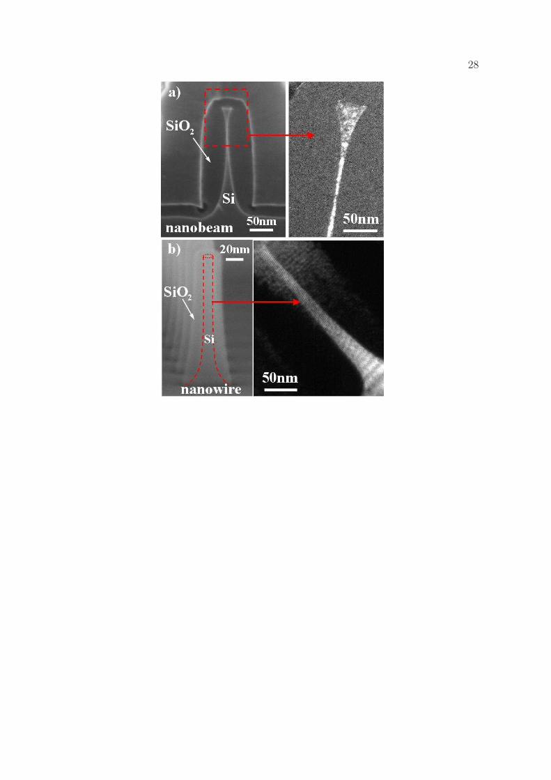
(width=53 nm) and nanowire (diameter=43 nm) in figure 8 emphasises the importance
of the dimensional aspect. While the two dimensional oxidised profile of the nanobeam
presents a characteristic non homogeneous anisotropic profile as explained in section 4.3,
the one dimensional nanowire has a very uniform shape. Despite the initial presence of
a convex shape at the bottom, the nanowire does not present a necklace shape (inset of
figure 8.(b) after oxidation which could indicate that a widespread compressive stress
take place around the nanowire. A common feature is the limited oxide growth observed
at the bottom end of the nanowire where the concave shape also influences the growth
by diffusion limited oxidation effects. However the effect seems to be less predominant
in the nanowire. The technical interest of the resulting silicon profile will be discussed
in section 5.
Self-limited or retarded effects during the oxidation of nanowire has been charac-
terised in details. Figure 9.(a) and .(b) present respectively the evolution of the SiNW
diameter and the oxide thickness as a function of the oxidation time. The experimental
dots give the remaining silicon diameter after oxidation and oxide stripping while the
dashed lines presents the simulated evolution obtained with the one dimensional model
discussed in section 3.2. Despite the rough approximation, since the experimental side-
walls of the nanowire are not strictly vertical, the one dimensional model is effective to
describe the oxidation kinetics. A slowdown of the oxidation kinetics has been identified.
Compared to the nanobeam oxidation, limited oxidation effects have been observed to
be highly dependent on the nanowire diameters. The evolution of the oxidation rate
for different SiNWs diameters shown in figure 9.(c) confirms these conclusions. While
initially being close to 3 nm/min., the rate decreases very quickly down to 1 nm/min.
This effect can be explained thanks to the compressive stress build-up provided in the
inset of figure 9.(c) which tends to decrease the linear oxidation rate as described in
(eq. 6). The normal radial stress at the silicon interface of the nanowire slows down the
oxidation rate by making the reaction of Si to SiO2 less energetically favourable. This
radial compressive stress build-up is much more effective here than in the nanobeam case
due to its more confined structure of the SiNWs. Figure 9.(d) describes the evolution of
the other kinetic parameter in the Deal and Grove framework, the parabolic rate. The
initial hydrostatic pressure at the Si/SiO2 interface being tensile, no diffusion limited
oxidation effect takes place. A significant oxide growth is necessary in order to change
the longitudinal stress from tensile to compressive and to reach a widespread compres-

12
sive hydrostatic pressure. The appearance of diffusion limited oxidation can explain the
quasi self-limited oxidation effects for the silicon nanowire with 40 min. of wet oxidation.
5. Silicon nanowires thinning and aspect ratio engineering
Vertical silicon nanowire arrays are a promising architecture for the implementation of
ultimate logic devices [53] or nanosensors and are routinely fabricated either by bottom-
up [54] or top-down approaches [23]. One of the key issues for all sub-20 nm devices
is the variability concern generated since large fluctuations of geometrical properties
(width, length, shape, gate oxide thickness) can be observed during the manufacturing
of a large number of these nanoobjects. A large impact on various electrical properties
(threshold voltage, geometry dependent capacitance) are expected [55]. Here, one of the
most difficult geometric parameters to control is the sidewall anisotropy ratio since near
vertical sidewall profile should be achieved with a small variability for the manufacturing
of vertical SiNWs based nanodevices.
Self-retarded silicon oxidation effects have been used to overcome the various
technological concerns since a better control of the nanowire radius and shape could
be achieved with the remaining silicon core. Figure 10.(a) details the experimental
evolution of the anisotropic character with the silicon diameter. An increase in the
anisotropic character is effectively observed for each nanowire, the effect for the thinnest
nanowire being more effective at least for the short oxidation time. After a wet oxidation
of 20 min. followed by an etching of the oxide layer, the anisotropy profile of SiNWs has
been improved from 92% up to 99% with the reduction of the SiNWs diameter (around
14 nm) for the thinnest nanowire (initially 33 nm). Insets (b) to (d) of figure 10 show
that the sidewall anisotropy of silicon nanowires has been effectively increased during
oxidation.
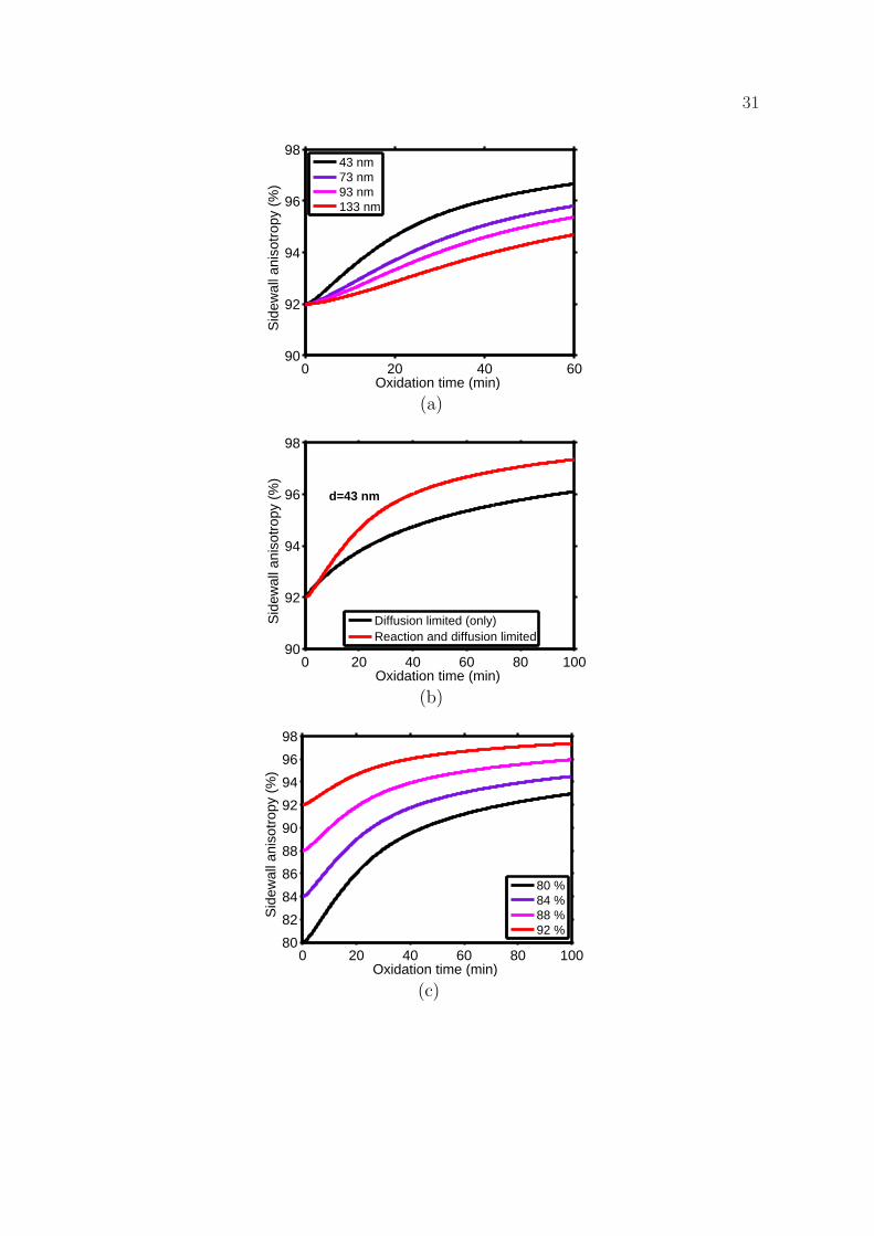
The modelling of the aspect ratio engineering is a complex task as a three dimen-
sional simulation of oxidation should be rigorously undertaken, as discussed in section
3.2. A first approximation has been undertaken by considering that the real nanowire is
made of several anisotropic nanowires of different diameters matching the initial exper-
imental aspect ratio. The theoretical improvement of the anisotropic character is given
in figure 11.(a). The model predicts effectively an increase in the aspect ratio from 92
% to up 94 % for 133 nm NWs or 96% for the thinnest 43 nm NWs. In agreement with
the experimental results, the aspect ratio increases for short oxidation times (below 20
min) and saturate with the dominance of diffusion limited oxidation effects. It could be
noticed that the model underestimates the aspect ratio improvement compared to the
experimental value since much more vertical sidewalls have been obtained experimen-
tally. Despite these limitations, some interesting conclusions for further experimental
work can be extracted. The importance to favour the reaction rate limited regime for
the sharpening of the aspect ratio is highlighted in figure 11.(b). The following scenario
has been investigated by simulation. A 43 nm diameter silicon nanowire free of stress

13
with a surrounding oxide of the same thickness has been considered. The presence of
this large oxide prevents an initial tensile hydrostatic pressure described in figure 9.(c)
and drives the appearance of retarded diffusion effects at the beginning of the oxidation
step. It can be observed that effectively, the aspect ratio engineering would be less effec-
tive compared to the standard case where initially only reaction rate limited oxidation
effects take place. This result would be of interest since oxidation/etching and stress
release could be foreseen in order to maximise the shape ratio engineering. Finally, the
impact of the initial anisotropic character has also been studied by simulation. The
results, given by figure 11.(c), show that the use of retarded oxidation effect would be
clearly beneficial when the anisotropic profile of vertical SiNWs decreases.
6. Conclusion
The modelling of retarded oxidation in various silicon nanostructures have been
investigated in depth based on a pragmatic approach that coupled 2D TCAD tools and
a one dimensional plastic model. Limits in the simulation and the parametrisation of
orientation effects and concave shape nanobjects have been emphasised. Large difference
in oxidation scheme for multidimensional nanostructures have been successfully
explained by modelling and in particular by the estimation of the radial stress build-
up. The engineering of the nanowire sharpening and the aspect ratio through retarded
oxidation effects have been demonstrated. The different simulations confirm some
experimental trends observed. The model also indicates that the initial regime where
reaction rate and diffusion limited effects due to the compressive radial stress build-up
is more favourable for the aspect ratio engineering of SiNWs.
Acknowledgments
This work was supported by the European Commission through the NANOSIL
Network of Excellence (FP7-IST-216171) and the RTB platform (French national
nanofabrication network, RENATECH). The financial support of ANR QUASANOVA
is also acknowledged.
References
[1] R. Okada and S. Iijima. Oxidation property of silicon small particles. Applied Physics Letters,
58(15):1662–1663, 1991.
[2] H. I. Liu, D. K. Biegelsen, N. M. Johnson, F. A. Ponce, and R. F. W. Pease. Self-limiting oxidation
of si nanowires. In Proceedings of the 16th international symposium on electron, ion, and photon
beams, volume 11, pages 2532–2537. AVS, 1993.
[3] H. Cui, C. X. Wang, and G. W. Yang. Origin of self-limiting oxidation of si nanowires. Nano
Letters, 8(9):2731–2737, 2008. PMID: 18680350.
[4] H. I. Liu, D. K. Biegelsen, F. A. Ponce, N. M. Johnson, and R. F. W. Pease. Self-limiting oxidation
for fabricating sub-5 nm silicon nanowires. Applied Physics Letters, 64(11):1383–1385, 1994.

14
[5] H. Heidemeyer, C. Single, F. Zhou, F. E. Prins, D. P. Kern, and E. Plies. Self-limiting and
pattern dependent oxidation of silicon dots fabricated on silicon-on-insulator material. Journal
of Applied Physics, 87(9):4580–4585, 2000.
[6] C. C. Buttner and M. Zacharias. Retarded oxidation of si nanowires. Applied Physics Letters,
89(26):263106, 2006.
[7] G. Pennelli. Top down fabrication of long silicon nanowire devices by means of lateral oxidation.
Microelectronic Engineering, 86(11):2139 – 2143, 2009.
[8] Y. Chen and Y. Chen. Modeling silicon dots fabrication using self-limiting oxidation.
Microelectronic Engineering, 57-58:897 – 901, 2001. Micro- and Nano-Engineering 2000.
[9] H. Coffin, C. Bonafos, S. Schamm, N. Cherkashin, G. Ben Assayag, A. Claverie, M. Respaud,
P. Dimitrakis, and P. Normand. Oxidation of si nanocrystals fabricated by ultralow-energy ion
implantation in thin sio[sub 2] layers. Journal of Applied Physics, 99(4):044302, 2006.
[10] G. Stan, S. Krylyuk, A. V. Davydov, and R. F. Cook. Compressive stress effect on the radial elastic
modulus of oxidized si nanowires. Nano Letters, 10(6):2031–2037, 2010. PMID: 20433162.
[11] Y.-M. Niquet, C. Delerue, and C. Krzeminski. Effects of strain on the carrier mobility in silicon
nanowires. Nano Letters, 12:3545, 2012.
[12] K. Trivedi, H. Yuk, H. C. F., M. J. Kim, and W. Hu. Quantum confinement induced performance
enhancement in sub-5-nm lithographic si nanowire transistors. Nano Letters, 11(4):1412–1417,
2011.
[13] X. Tang, N. Reckinger, V. Bayot, C. Krzeminski, E. Dubois, A. Villaret, and D.-C. Bensahel.
Fabrication and room-temperature single-charging behavior of self-aligned single-dot memory
devices. Nanotechnology, IEEE Transactions on, 5(6):649 –656, nov. 2006.
[14] X. Tang, C. Krzeminski, A. Lecavelier des Etangs-Levallois, Z. Chen, E. Dubois, E. Kasper,
A. Karmous, N. Reckinger, D. Flandre, L. A. Francis, J.-P. Colinge, and J.-P. Raskin. Energy-
band engineering for improved charge retention in fully self-aligned double floating-gate single-
electron memories. NanoLetters, 11:4520–4526, 2011.
[15] C. Krzeminski, X. Tang, N. Reckinger, V. Bayot, and E. Dubois. Process optimization and
downscaling of a single-electron single dot memory. Nanotechnology, IEEE Transactions on,
8(6):737 –748, nov. 2009.
[16] J. Dalla Torre, J.-L. Bocquet, Y. Limoge, J.-P. Crocombette, E. Adam, G. Martin, T. Baron,
P. Rivallin, and P. Mur. Study of self-limiting oxidation of silicon nanoclusters by atomistic
simulations. Journal of Applied Physics, 92(2):1084–1094, 2002.
[17] B.-H. Kim, M. A. Pamungkas, M. Park, G. Kim, K.-R. Lee, and Y.-C. Chung. Stress evolution
during the oxidation of silicon nanowires in the sub-10 nm diameter regime. Applied Physics
Letters, 99(14):143115, 2011.
[18] T. Watanabe. Dynamic bond-order force field. Journal of Computational Electronics, 10:2–20,
2011.
[19] V. Senez, D. Collard, B. Baccus, and J. Lebailly. Analysis and application of a viscoelastic model
for silicon oxidation. J. Appl. Phys., 76:3285, 1994.
[20] F.-J. Ma, S. C. Rustagi, G. S. Samudra, H. Zhao, N. Singh, G.-Q. Lo, and D.-L. Kwong. Modeling
of stress-retarded thermal oxidation of nonplanar silicon structures for realization of nanoscale
devices. IEEE Electron Device Letters, 31(7):719, 2010.
[21] D.-B. Kao, J.P. McVittie, W.D. Nix, and K.C. Saraswat. Two-dimensional thermal oxidation of
silicon;i. experiments. Electron Devices, IEEE Transactions on, 34(5):1008 – 1017, may 1987.
[22] D.-B. Kao, J.P. McVittie, W.D. Nix, and K.C. Saraswat. Two-dimensional thermal oxidation
of silicon. ii. modeling stress effects in wet oxides. Electron Devices, IEEE Transactions on,
35(1):25 –37, jan 1988.
[23] X.-L. Han, G. Larrieu, P.-F. Fazzini, and E. Dubois. Realization of ultra dense arrays of vertical
silicon nanowires with defect free surface and perfect anisotropy using a top-down approach.
Microelectronic Engineering, 88(8):2622 – 2624, 2011.
[24] Ricardo Garcia, Montserrat Calleja, and Heinrich Rohrer. Patterning of silicon surfaces with

15
noncontact atomic force microscopy: Field-induced formation of nanometer-size water bridges.
Journal of Applied Physics, 86(4):1898–1903, 1999.
[25] Ricardo Garcia, Ramses V. Martinez, and Javier Martinez. Nano-chemistry and scanning probe
nanolithographies. Chem. Soc. Rev., 35:29–38, 2006.
[26] J. Martinez, R. V. Martnez, and R. Garcia. Silicon nanowire transistors with a channel width of
4 nm fabricated by atomic force microscope nanolithography. Nano Letters, 8(11):3636–3639,
2008. PMID: 18826289.
[27] I. J. R. Baumvol. Atomic transport during growth of ultrathin dielectrics on silicon. Surface
Science Reports, 36(1-8):1 – 166, 1999.
[28] B. E. Deal and A. S. Grove. General relationship for the thermal oxidation of silicon. Journal of
Applied Physics, 36(12):3770–3778, 1965.
[29] S. M. Hu. Effect of process parameters on stress development in two-dimensional oxidation.
Journal of Applied Physics, 64(1):323–330, 1988.
[30] J. R. Ligenza. Effect of crystal orientation on oxidation rates of silicon in high pressure steam.
The Journal of Physical Chemistry, 65(11):2011–2014, 1961.
[31] T. Hoffmann, K. F. Dombrowski, and V. Senez. On 2d/3d numerical oxidation modeling:
Calibration and investigation of silicon crystal orientation effect on stresses in shallow trench
isolations. Technical Proceedings of the 2000 International Conference on Modeling and
Simulation of Microsystems, Chap. 2:p. 59–62, 2000.
[32] C. S. Rafferty, L. Borucki, and R. W. Dutton. Plastic flow during thermal oxidation of silicon.
Applied Physics Letters, 54:1516, 1989.
[33] C. S. Rafferty and R. W. Dutton. Plastic analysis of cylinder oxidation. Applied Physics Letters,
54:1815, 1989.
[34] S. Bozek, B. Baccus, V. Senez, and Z. Z. Wang. Mesh generation for 3D process simulation and
the moving boundary problem. Simulation of semiconductors devices and processes, 6:460, 1995.
[35] A. Marmiroli, G. Carnevale, and A. Ghetti. Technology and device modeling in micro and nano-
electronics: Current and future challenges. 11:p. 41–54, 2007.
[36] M. E. Law. Process modeling for future technologies. IBM J. Res. Dev., 46:339–346, March 2002.
[37] TSUPREM-4, SYNOPSYS TCAD.
[38] V. Senez, D. Collard, P. Ferreira, and B. Baccus. Two-dimensional simulation of local oxidation
of silicon: calibrated viscoelastic flow analysis. IEEE Transactions on Electron Devices, 43:720–
731, May 1996.
[39] R. H. Doremus. Oxidation of silicon: strain and linear kinetics. Thin Solid Films, 122:191–196,
1984.
[40] G. Hetherington, K. H. Jack, and J. C. Kennedy. The viscosity of vitreous silica. Phys. Chem.
Glasses, 5:130, 1964.
[41] T. Uchida and K. Nishi. Formulation of a viscoelastic stress problem using analytical integration
and its application to viscoelastic oxidation simulation. Jpn. J. Appl. Phys., 40:p. 6711–6719,
2001.
[42] P.-F. Fazzini, C. Bonafos, A. Claverie, A. Hubert, T. Ernst, and M. Respaud. Modeling stress
retarded self-limiting oxidation of suspended silicon nanowires for the development of silicon
nanowire-based nanodevices. Journal of Applied Physics, 110:033524, 2011.
[43] C. Krzeminski, X.-L. Han, and G. Larrieu. Understanding of the retarded oxidation effects in
silicon nanostructures. Applied Physics Letters, 100(25):263111, 2012.
[44] E. A Irene, H. Z. Massoud, and E. Tierney. Silicon oxidation studies: Silicon orientation effects
on thermal oxidation. J. Electrochem. Soc., 133(6):1253, 1986.
[45] J. L. Ngau, P. B. Griffin, and J. D. Plummer. Silicon orientation effects in the initial regime of
wet oxidation. Journal of The Electrochemical Society, 149(8):F98–F101, 2002.
[46] E. Kodeba and E. A. Irene. Intrinsic sio2 film stress measurements on thermall oxidized si. J.
Vac. Sci. Technol. B, 5(1):15, 1987.
[47] E. Kodeba and E. A. Irene. in-situ stress measurements during thermal oxidation of silicon. J.

16
Vac. Sci. Technol. B, 7(2):163, 1989.
[48] T. J Delph. Intrinsic strain in sio2 thin films. J. Appl. Phys., 83(2):786, 1998.
[49] R. B. Marcus and T. T. Sheng. The oxidation of shaped silicon surfaces. J. Electrochem. Soc.,
129(6):1278, 1982.
[50] L. O. Wilson and R. B. Marcus. Oxidation of curved silicon surfaces. J. Electrochem. Soc.,
134(2):481, 1987.
[51] P. Sutardja and W. G. Oldham. Modeling of stress effects in silicon oxidation. IEEE Trans. elect.
Devices, 36:2415, 1989.
[52] A. Poncet. Finite-element simulation of local oxidation of silicon. IEEE Trans. on Computer-aided
Design, 4(1):41, 1985.
[53] G. Larrieu and X.-L. Han. Vertical nanowire array-based field effect transistors for ultimate scaling.
Nanoscale, 5:2437–2441, 2013.
[54] V. Schmidt, H. Riel, S. Senz, S. Karg, W. Riess, and U. Gsele. Realization of a silicon nanowire
vertical surround-gate field-effect transistor. Small, 2(1):85–88, 2006.
[55] C.-W. Sohn, C. Y. Kang, R.-H. Baek, D.-Y. Choi, H. C. Sagong, E.-Y. Jeong, J.-S. Lee, P. Kirsch,
R. Jammy, J.C. Lee, and Y.-H. Jeong. Comparative study of geometry-dependent capacitances
of planar fets and double-gate finfets: Optimization and process variation. In VLSI Technology,
Systems, and Applications (VLSI-TSA), 2012 International Symposium on, pages 1 –2, april
2012.

17
Tables
(B/A)0 E(B/A) f100 f110 f111(µm/min) (eV)
Standard 2.058 1004 1.17 1 1.676 1.394
Modif. 2.058 1004 1.17 1 2.25 1.57
Table 1. Prefactors (B/A)0 and activation energies E(B/A) for the Arrhenius
expression of the linear rate constant for the Deal and Grove model. Standard
TCAD and modified parameters to take into account the orientation influence are
given respectively in the first and second lines of the table.

18
7. Captions

19
Figure 1. Top-down fabrication process of the different silicon nanostructures
investigated in this work for nanobeams, nanowires and nanorings. Serial A : SEM
pictures in cross view of HSQ mask (1) nanobeam, (2) nanopillars and (3) nanoring;
Serial B(1-3): SEM pictures after mask transfer by etching in Si substrate; Serial
C(1-3): SEM pictures after wet oxidation and strepping oxide by HF.
Figure 2. Schematic of the different systems considered in this work. a) describes the
planar bulk oxidation system in order to simulate the oxide bulk growth. b) presents
the 2D nanobeam oxidation process where FEM simulations have been undertaken in
order to predict the complex oxide film shape. (c) presents the cylinder geometry used
for the simulation of the nanowire oxidation. An infinite length nanowire is considered.
Figure 3. Influence of substrate orientations for planar wet oxidation at 850◦C. The
experimental data of Ngau et al. performed at a lower temperature (785◦C) are also
reported in black symbols [45] whereas modelling results are given in dashed lines.
(a) presents in dashed lines the simulation results for the standard Deal and Grove
model whereas b) highlights the agreement when the standard linear growth rates are
adjusted in order to take into account the influence of the enhanced oxidation for [110]
in the short time regime. Similar conclusions to the study of Ngau et al. are reached.
Figure 4. Experimental oxidation behaviour for convex and concave silicon
nanostructures at 850◦C (symbols). Comparison of retarded oxidation effects in
the convex/concave cases predicted by the analytic approach using the standard
activation volume of TCAD tools based on the viscoelastic model [19] (Vd=75 A3)
and the activation volume used in this work (Vd=45 A3) (lines). a) highlights the
retardation is well described for convex geometry but clearly overestimated for the
concave nanoobjects. b) shows that a proper calibration of the standard activation
volume (Vd=45 A3) is necessary in order to describe the influence of concave effects.
Figure 5. (a) Oxide thickness as a function of the nanobeam width for two oxidation
times (10 min black color) and 20 min (red color)). The open symbols for the
thinnest nanobeams indicate a complete oxidation at mid-height with the presence
of a embedded silicon nanowire at the top. (b) presents the characteristics of the
nanobeam profile with the influence of the convex (resp. concave) corner influence at
the top (resp. bottom). (c) Different SEM images showing the influence of the height
and oxidation duration on the nanobeam structure after wet oxidation.
Figure 6. (a)/(c) : SEM images and (b)/(d) 2D FEM simulations of 40 nm
wide nanobeams (height 220 nm) for 10 min/20 min of wet oxidation. (b) the two
dimensional FEM simulation counterpart. (c) and (d) presents the same properties
(structure and simulation) but for 20 min of wet oxidation. The lateral strain
distribution σxx is reported. It shows that a significant compressive strain (above
2 GPa) is obtained at the bottom and the top of the nanobeam explaining the limited
oxide growth and the oxide embedded NWs at the top for 20 minutes. For figures (c)
& (d), the agreement between the simulation and the SEM image and the presence of
a SiNW on the top could be emphasised.

20
Figure 7. (a) Theoretical oxide thickness predicted by process simulation as a function
of the nanobeam width for respectively 110 and 240 nm height nanobeams. The
simulation confirms the main experimental trend with constant oxide thickness as
function of the nanobeam widths. For 20 min of wet oxidation some difference is
observed between 110 and 240 nm height nanobeams which can be related to stress
effects. (b) presents the lateral stress building with the oxidation time as function
of the nanobeam height. The large stress building for the 110 nm height which
explains the modest oxide thickness increase between 10 and 20 min and the difference
with the 240 nm nanobeam height. (c) The lateral stress σxx dependence with the
nanobeam geometry is relatively constant along nanobeams width, which explains the
experimental trend described in 5.(a).
Figure 8. The different SEM images compare the shape for (a) the nanobeam and
(b) the nanowire profile. The TEM characterisation in (a) shows that the nanobeam
top has a neck shape whereas (b) presents a vertical uniform profile of the nanowire.
Figure 9. (a) The various symbols report the experimental SiNWs diameters evolution
with oxidation for starting 43, 73, 93 and 133 nm diameter which compare well
with the 1D modelling counterpart. (b) reports the evolution of experimental and
theoretical thickness for the same conditions. (c) describes the linear rate for the
different SiNWs with in inset the compressive radial stress building which govern the
linear rate decrease. (d) reports the parabolic rate constant for the SiNWs and the
hydrostatic pressure variation with the oxidation time (in inset).
Figure 10. Experimental improvement of the silicon nanowires aspect ratio by
oxidation. (a) The various symbols report the experimental aspect ratio variation
with the silicon nanowire diameters (93 nm down to 33 nm) for respectively 10 min.
and 20 min. of wet oxidation. The dashed lines correspond to the experimental trend.
The retarded oxidation effects are able to increase significantly the initial ratio aspect
above 92 % (b) presents the SEM images of silicon nanowires before the oxidation step
while (c) and (d) describe the aspect ratio engineering of the oxidised silicon nanowires
(scale bar=100nm).
Figure 11. (a) Variation of the anisotropic aspect ratio for the different SiNWs
estimated by the 1D plastic model. The model underestimates the experimental
increase in the aspect ratio presented in figure 10. The effect of the retarded oxidation
is beneficial for the thinnest SiNWs as observed experimentally. (b) Comparison
between the anisotropic character evolution for a configuration where a 43 nm diameter
nanowire with no initial oxide and a theoretical configuration where a large initial
silicon oxide exceeding the silicon core would be present. (c) The variations with
oxidation are reported as a function of the initial anisotropic character.

21

22
SiO
Si [100], Si [110], Si [111]
2
2H O
y
x
Planar bulk oxidation(a)
2H O
y
x
Nanobeam oxidation(b)
θ
rzu
u
u
b
a
Si
SiO2
Cylinder shape oxidation(c)
1

23
0 20 40 60 800
20
40
60
80
100
Time (min)
Oxi
de T
hick
ness
(nm
)
785°C
850°C
[110] [111] [100]
[110]
[111]
[100]
(a)
0 20 40 60 800
20
40
60
80
100
Time (min)
Oxi
de T
hick
ness
(nm
)
785°C
850°C
[110] [111] [100]
[110]
[111]
[100]
(b)

24
0 10 20 30 40 500
20
40
60
Time (min)
Oxi
de th
ickn
ess
(nm
)
φ=70nm
φ=130nm
φinner
=70nm
φinner
=430nm
Si bulk (110)ConvexConcave
(a)
0 10 20 30 40 500
20
40
60
Time (min)
Oxi
de th
ickn
ess
(nm
)
φ=70nm
φ=130nm
φinner
=70nm
φinner
=430nm
Si bulk (110)ConvexConcave
(b)

25
10 30 50 70 90 11020
30
40
50
60
Nanobeam width (nm)
Oxi
de th
ickn
ess
(nm
)
850°C
Si bulk (110)
Si bulk (110)
H=110nm
H=240nm
H=110nm
H=240nm20 min.
10 min.
(a)
(b)
(c)

26
(a)
500 MPa−2 GPa
0−100 MPa
100−500 MPa
−0.1−0.2
0
−0.1
−0.2
0.1
2GPa−500 MPa
500−100 MPa
100−0 MPa
0 0.1 0.2
σXX
Compression
Tension
(b)
(c)
Compression
500 MPa−2GPa
100−500 MPa
0−100 MPa
Tension0−100 MPa
2GPa−500MPa
0−0.2 −0.1−0.2
0
500−100 MPa
−0.1
−0.2
σ
0.10.1 0.2
XX
(d)

27
20 40 60 80 10020
40
60
80
Nanobeam width (nm)
Oxi
de th
ickn
ess
(nm
)
[110] Bulk 10 min
[110] Bulk 20 min
110nm (10 min)240nm (10 min)110nm (20 min)240nm (20 min)
(a)
0 5 10 15 20−2
−1
0
1
2
Oxidation Time (min)
Late
ral s
tres
s σ xx
(G
Pa)
55nm110nm175nm240nm
(b)
20 40 60 80 100−4
−2
0
2
4
Nanobeam width (nm)
Late
ral S
tres
s σ xx
(G
Pa)
10 min
20 min
110 nm (10 min)110 nm (20 min)240 nm (10 min)240 nm (20 min)
(c)
28

29
0 10 20 30 400
30
60
90
120
150
850°C
43 nm
73 nm
93 nm
133 nm
Oxidation time (min)
NW
s di
amet
er (
nm)
(a)
0 10 20 30 400
20
40
60
850°C
43 nm
73 nm
93 nm
133 nm
Oxidation time (min)
Oxi
de th
icke
ss (
nm)
(b)
0 10 20 30 400
1
2
3
Oxidation time (min)
Line
ar r
ate
(nm
/min
)
43 nm73 nm93 nm133 nm
0 10 20 30 40−3
−2
−1
0
Oxidation Time (min.)
Rad
ial s
tres
s (G
Pa)
(c)
0 10 20 30 40
4
8
12x 10
4
Oxidation time (min)
Par
abol
ic r
ate
(nm
2 /min
)
43 nm73 nm93 nm133 nm
0 10 20 30 40−1
0
1
2
Oxidation time (min)
Hyd
rost
atic
pre
ssur
e (G
Pa)
(d)

30
0 5 10 15 2090
92
94
96
98
100
Oxidation time (min)
Sid
ewal
l ani
sotr
opy
(%)
33nm43nm73nm93nm
(a)
(b) (c) (d)
31
0 20 40 6090
92
94
96
98
Oxidation time (min)
Sid
ewal
l ani
sotr
opy
(%)
43 nm73 nm93 nm133 nm
(a)
0 20 40 60 80 10090
92
94
96
98
Oxidation time (min)
Sid
ewal
l ani
sotr
opy
(%)
d=43 nm
Diffusion limited (only)Reaction and diffusion limited
(b)
0 20 40 60 80 10080
82
84
86
88
90
92
94
96
98
Oxidation time (min)
Sid
ewal
l ani
sotr
opy
(%)
80 %84 %88 %92 %
(c)