Embed Size (px)
Citation preview
Supplementary Information for
Transparent-Flexible-Multimodal Triboelectric Nanogenerators for
Mechanical Energy Harvesting and Self-powered Sensor
Applications
Qitao Zhou1†, Jun Gyu Park1†, Kyeong Nam Kim2, Ashish Kumar Thokchom1, Juyeol Bae1, Jeong Min Baik2* and Taesung Kim1,3*
1Department of Mechanical Engineering, Ulsan National Institute of Science and Technology (UNIST), 50 UNIST-gil, Ulsan 44919, Republic of Korea.
2School of Materials Science and Engineering, KIST-UNIST Ulsan Center for Convergent Materials, Ulsan National Institute of Science and Technology, Ulsan 44919, Republic of Korea
3Department of Biomedical Engineering, Ulsan National Institute of Science and Technology (UNIST), 50 UNIST-gil, Ulsan 44919, Republic of Korea
*CORRESPONDENCE:
Taesung KimDepartment of Mechanical EngineeringUlsan National Institute of Science and Technology (UNIST)50 UNIST-gil, Ulsan 44919, Republic of KoreaE-mail: [email protected]: +82-52-217-2313; Fax: +82-52-217-2409
Jeong Min BaikSchool of Materials Science and Engineering, KIST-UNIST-Ulsan Center for Convergent MaterialsUlsan National Institute of Science and Technology (UNIST)Ulsan 689-798, KoreaE-mail: [email protected]: +82-52-217-2324; Fax: +82-52-217-2309
1
Supplementary Table
Table S1. Comparison of the key properties among FTCEs fabricated by various materials and
methods.
Materials Sheet resistanceRs (Ω/sq)
Transmittance at550 nm [%]
Reference
Reduced graphene oxide films 1800 81 [1]Graphene Films 230 72 [2]Carbon nanotube films 160 87 [3]Pt nanobelt network 16 83 [4]Ag nanowire network 71.2 87.7 [5]Ag grid 30 85 [6]Cu film with hole arrays 17.48 83 [7]Ag film with pore arrays 18.5 93.1 This workBare Ag film (15 nm) 7.4 67.2 This work
2
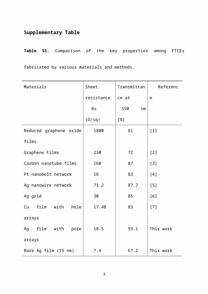
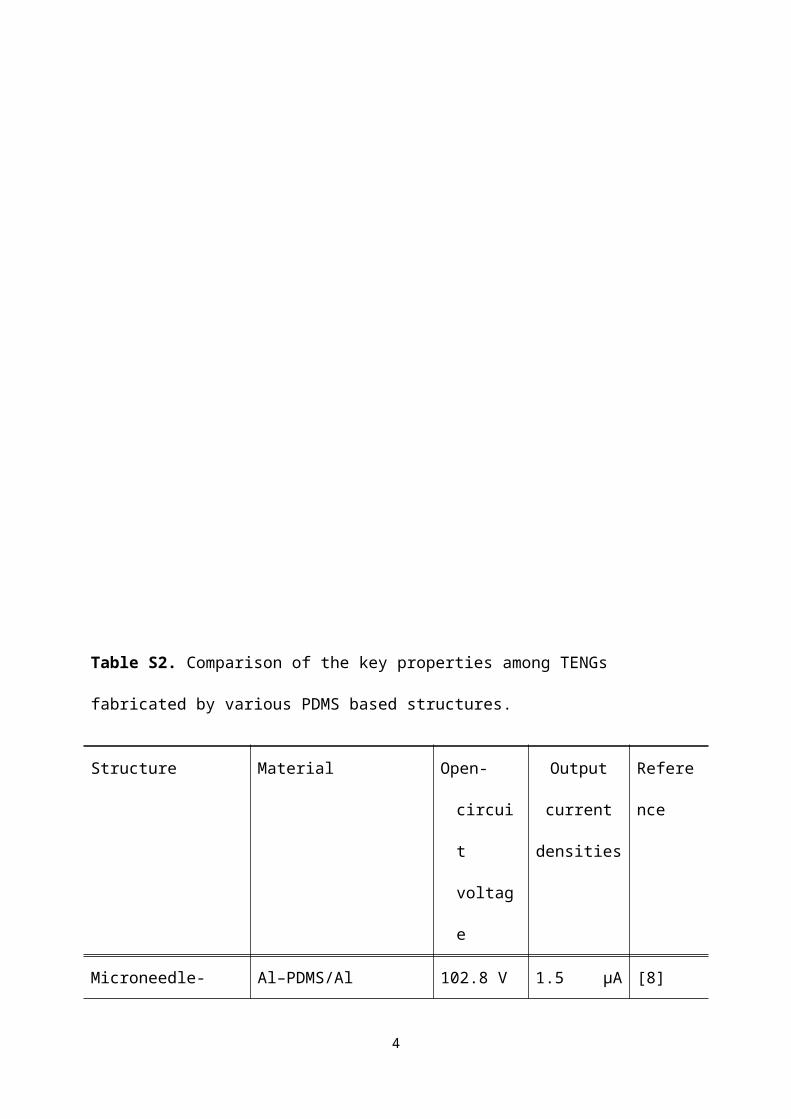
Table S2. Comparison of the key properties among TENGs fabricated by various PDMS based structures.
Structure Material Open-circuit voltage
Output current
densities
Reference
Microneedle-StructuredPDMS
Al–PDMS/Al 102.8 V 1.5 µA cm2 [8]
Cicada wing replicated PDMS structures
Cu–PDMS/Au 210 V 3.68 μA/cm2 [9]
PDMS nano-pillar Al/PDMS–Ni ~100 V[10]
Pyramid-featured PDMS
Indium tin oxide (ITO)/PET–PDMS/PET/ITO
18 V ∼0.13 μA/cm2
[11]
PDMS with hierarchical surfacemorphology
Al–PDMS/Al 207 V 14.1 μA/cm2 [12]
PDMS pyramid patterns
Electrode/Kapton/PDMS–Al with cubic patterns
230 V 15.5 μ A/cm2 [13]
PDMS porous Pyramid patterns
Ag/PET–PDMS/Ag/PET 80.8 V 28.4 μ A/cm2 This work
3
Supplementary Figures
Fig. S1. SEM images of PMMA patterns printed on the PET substrate with different voltage. (a) 23 V, (b) 35 V. The corresponding center-to-center spacing distances set as 100 μm. Scale bars are 100 μm.
4
Fig. S2. SEM images of PMMA patterns printed on the PET substrate with different center to center distances between the printing drops. (a-c) The corresponding center-to-center spacing distances set as 110 μm, 100 μm and 90 μm. Scale bars are 100 μm.
5

Fig. S3. (a) Schematic of fabrication process for transparent denticulate Ag microwire arrays, and corresponding SEM image (b). (c) and (d) are photographs of FTCEs consisted of denticulate Ag microwires before and after removing the PMMA patterns.
6
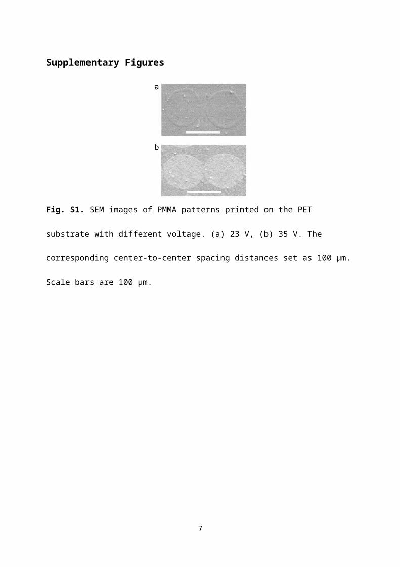
Fig. S4. SEM images of the Ag film with pore patterns fabricated on PDMS and the close-up view.
7
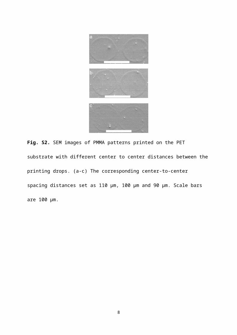
Fig. S5. Schematic illustration of the structure of the four-wire touch screen fabricated in this work. The right lower picture shows the connection between the TSP and controller board. The controller board connect with a computer by a USB cable.
8
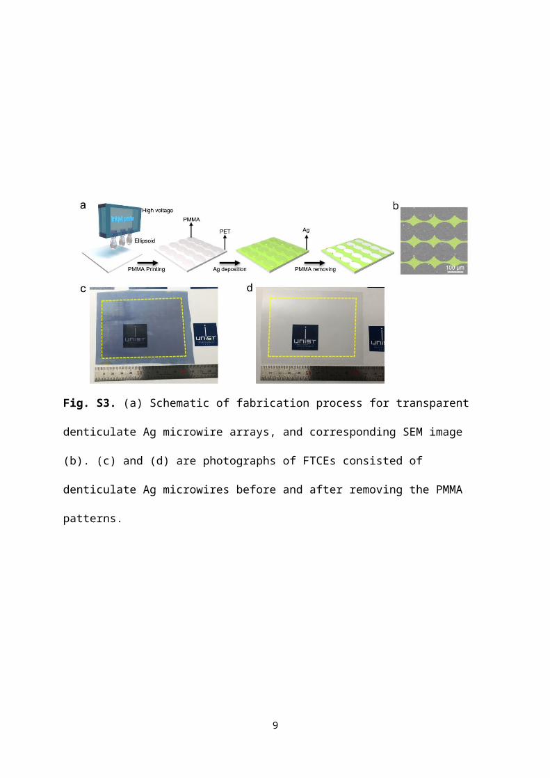
Fig. S6. (a-c) SEM images of the photoresist grids after slide coating PS particles with concentrations of 2.6 wt%, 5.2 wt% and 10.4 wt%, respectively. (d-f) The SEM images of corresponding PDMS replicas. The depth of the photoresist is 10 μm. Scale bars are 10 μm.
9
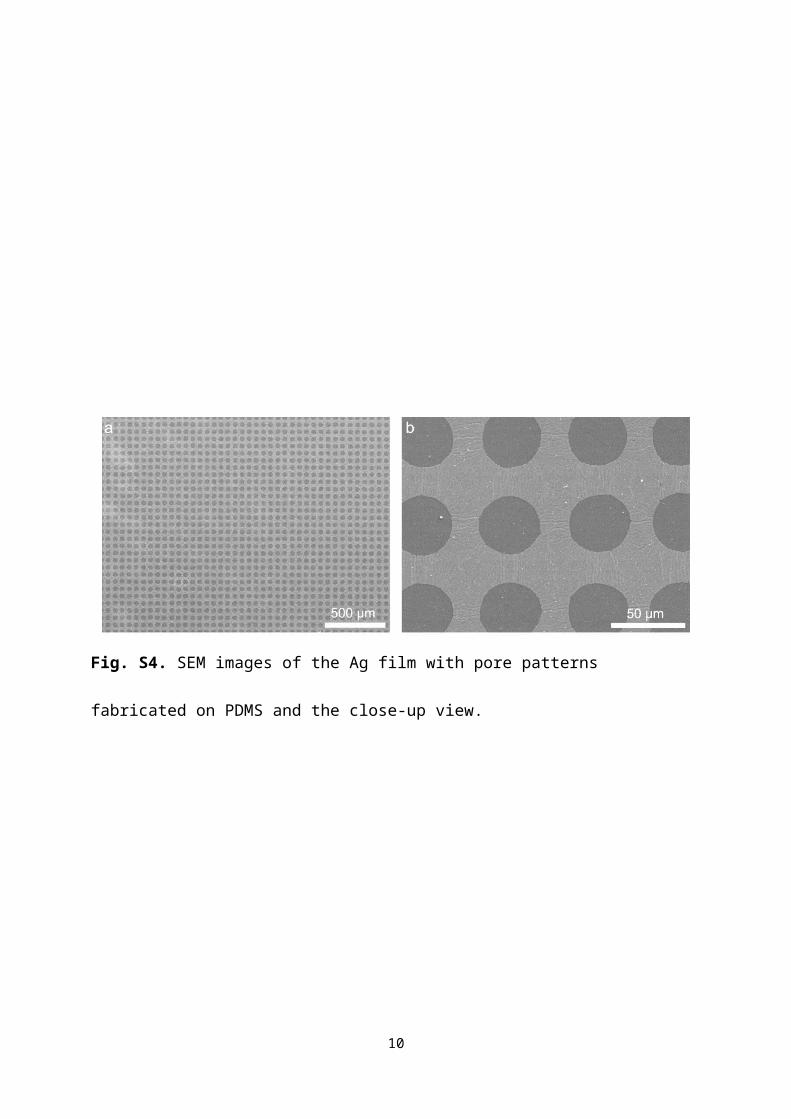
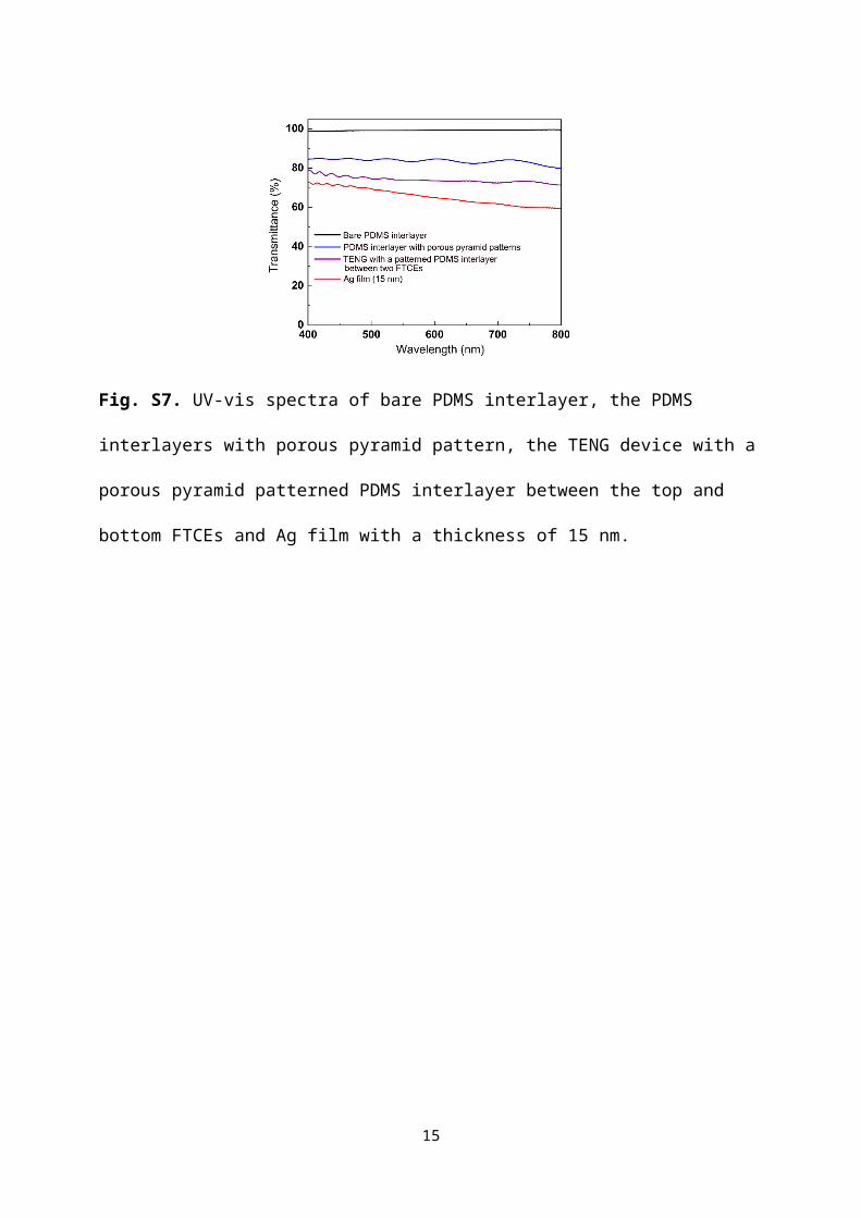
Fig. S7. UV-vis spectra of bare PDMS interlayer, the PDMS interlayers with porous pyramid pattern, the TENG device with a porous pyramid patterned PDMS interlayer between the top and bottom FTCEs and Ag film with a thickness of 15 nm.
10

Fig. S8. (a) Open-circuit voltage, and (b) output current densities of the porous pyramid based TENG under working frequencies of 2 Hz and force of 10 N.
11
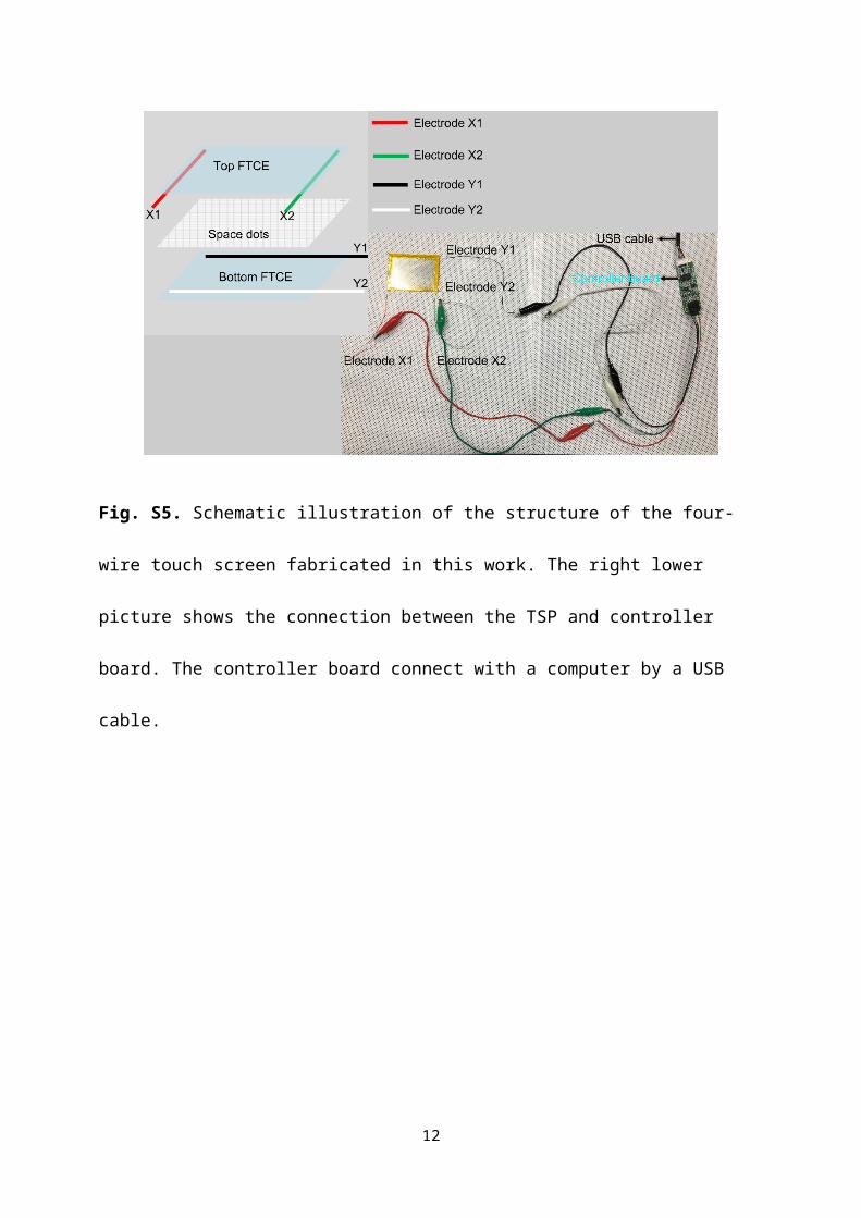
Fig. S9. (a) Open-circuit voltage, and (b) output current densities of from the non-transparent electrode and PDMS pair under working frequencies of 10 Hz and force of 22 N.
12
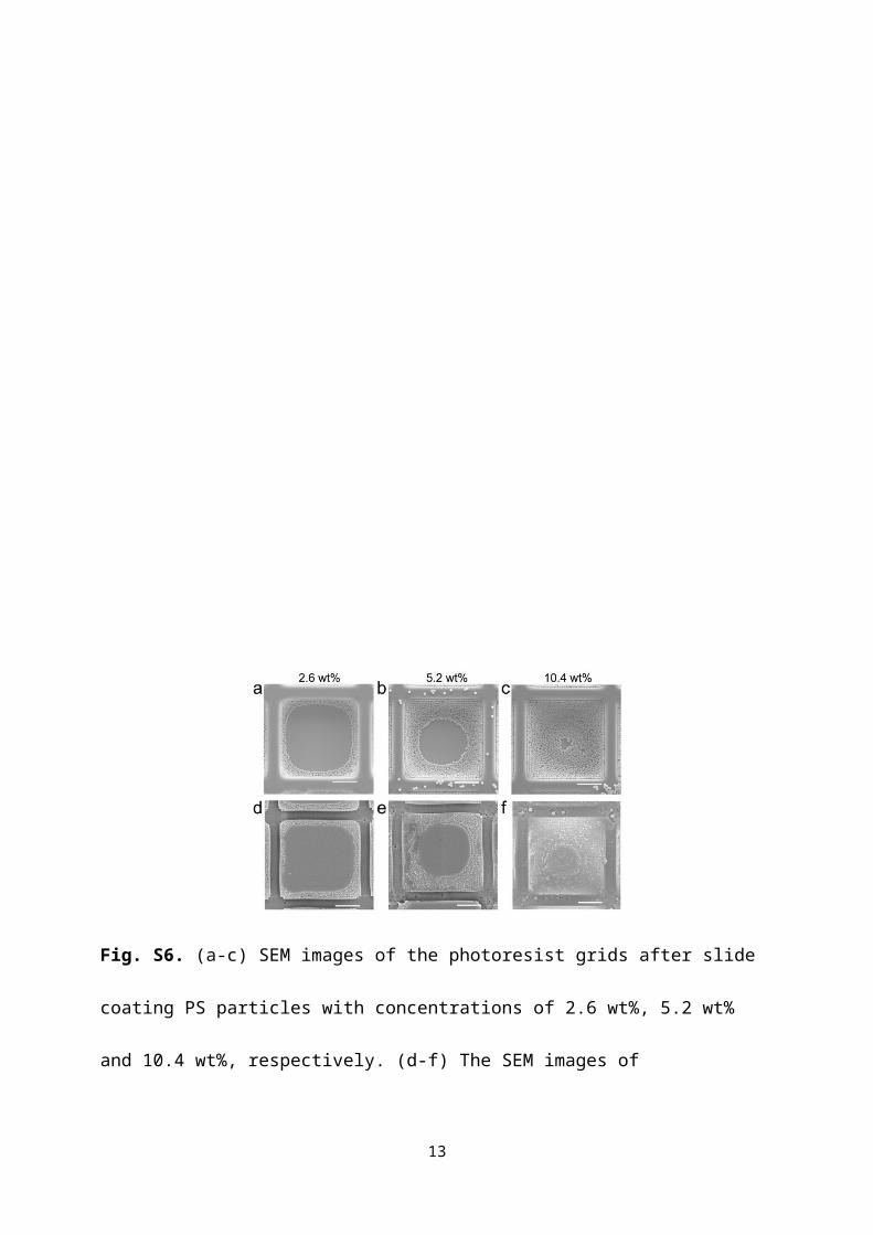
Fig. S10. The measured voltage of a commercial capacitor (1000 μF) charged with AC to DC signal converting circuit.
13

Fig. S11. Optical transmittance of the transparence of the single-electrode-based TENG.
14
Reference
[1] X. Wang, L. Zhi, K. Müllen, Transparent, conductive graphene electrodes for dye-sensitized solar cells, Nano Lett. 8 (2008) 323-327.[2] L. Gomez De Arco, Y. Zhang, C.W. Schlenker, K. Ryu, M.E. Thompson, C. Zhou, Continuous, highly flexible, and transparent graphene films by chemical vapor deposition for organic photovoltaics, ACS Nano 4 (2010) 2865-2873.[3] D. Zhang, K. Ryu, X. Liu, E. Polikarpov, J. Ly, M.E. Tompson, et al., Transparent, conductive, and flexible carbon nanotube films and their application in organic light-emitting diodes, Nano Lett. 6 (2006) 1880-1886.[4] Y. Wang, J. Cheng, Y. Xing, M. Shahid, H. Nishijima, W. Pan, Stretchable Platinum Network-Based Transparent Electrodes for Highly Sensitive Wearable Electronics, Small 13 (2017) 1604291.[5] C. Chen, Y. Zhao, W. Wei, J. Tao, G. Lei, D. Jia, et al., Fabrication of silver nanowire transparent conductive films with an ultra-low haze and ultra-high uniformity and their application in transparent electronics, J. Mater. Chem. C 5 (2017) 2240-2246.[6] S. Hong, J. Yeo, G. Kim, D. Kim, H. Lee, J. Kwon, et al., Nonvacuum, maskless fabrication of a flexible metal grid transparent conductor by low-temperature selective laser sintering of nanoparticle ink, ACS Nano 7 (2013) 5024-5031.[7] D. Paeng, J.-H. Yoo, J. Yeo, D. Lee, E. Kim, S.H. Ko, et al., Low-Cost Facile Fabrication of Flexible Transparent Copper Electrodes by Nanosecond Laser Ablation, Adv. Mater. 27 (2015) 2762-2767.[8] V.-L. Trinh, C.-K. Chung, A Facile Method and Novel Mechanism Using Microneedle-Structured PDMS for Triboelectric Generator Applications, Small 13 (2017) 1700373.[9] M.-L. Seol, J.-H. Woo, D.-I. Lee, H. Im, J. Hur, Y.-K. Choi, Nature-Replicated Nano-in-Micro Structures for Triboelectric Energy Harvesting, Small 10 (2014) 3887-3894.[10] H.-J. Choi, J.H. Lee, J. Jun, T.Y. Kim, S.-W. Kim, H. Lee, High-performance triboelectric nanogenerators with artificially well-tailored interlocked interfaces, Nano Energy 27 (2016) 595-601.[11] F.-R. Fan, L. Lin, G. Zhu, W. Wu, R. Zhang, Z.L. Wang, Transparent Triboelectric Nanogenerators and Self-Powered Pressure Sensors Based on Micropatterned Plastic Films, Nano Lett. 12 (2012) 3109-3114.[12] D. Jang, Y. Kim, T.Y. Kim, K. Koh, U. Jeong, J. Cho, Force-assembled triboelectric nanogenerator with high-humidity-resistant electricity generation using hierarchical surface morphology, Nano Energy 20 (2016) 283-293.[13] S. Wang, L. Lin, Z.L. Wang, Nanoscale Triboelectric-Effect-Enabled Energy Conversion for Sustainably Powering Portable Electronics, Nano Lett. 12 (2012) 6339-6346.
15