Embed Size (px)
Citation preview
ARM7TDMI Data SheetARM DDI 0029E
4-1
111
Ope
n A
cces
s
ARM Instruction Set
This chapter describes the ARM instruction set.
4.1 Instruction Set Summary 4-2
4.2 The Condition Field 4-5
4.3 Branch and Exchange (BX) 4-6
4.4 Branch and Branch with Link (B, BL) 4-8
4.5 Data Processing 4-10
4.6 PSR Transfer (MRS, MSR) 4-18
4.7 Multiply and Multiply-Accumulate (MUL, MLA) 4-23
4.8 Multiply Long and Multiply-Accumulate Long (MULL,MLAL) 4-25
4.9 Single Data Transfer (LDR, STR) 4-28
4.10 Halfword and Signed Data Transfer 4-34
4.11 Block Data Transfer (LDM, STM) 4-40
4.12 Single Data Swap (SWP) 4-47
4.13 Software Interrupt (SWI) 4-49
4.14 Coprocessor Data Operations (CDP) 4-51
4.15 Coprocessor Data Transfers (LDC, STC) 4-53
4.16 Coprocessor Register Transfers (MRC, MCR) 4-57
4.17 Undefined Instruction 4-60
4.18 Instruction Set Examples 4-61
4
ARM Instruction Set - Summary
ARM7TDMI Data SheetARM DDI 0029E
4-2
Ope
n A
cces
s
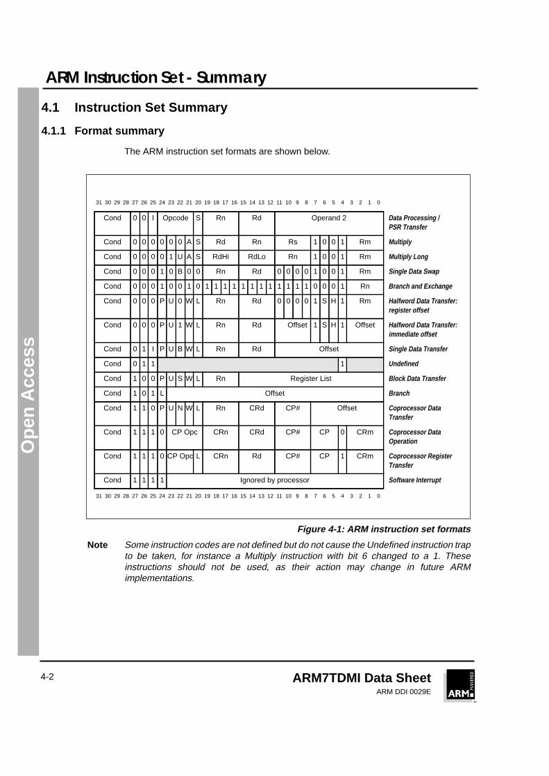
4.1 Instruction Set Summary
4.1.1 Format summary
The ARM instruction set formats are shown below.
Figure 4-1: ARM instruction set formats
Note Some instruction codes are not defined but do not cause the Undefined instruction trapto be taken, for instance a Multiply instruction with bit 6 changed to a 1. Theseinstructions should not be used, as their action may change in future ARMimplementations.
31 30 29 28 27 26 25 24 23 22 21 20 19 18 17 16 15 14 13 12 11 10 9 8 7 6 5 4 3 2 1 0
Cond 0 0 I Opcode S Rn Rd Operand 2 Data Processing /PSR Transfer
Cond 0 0 0 0 0 0 A S Rd Rn Rs 1 0 0 1 Rm Multiply
Cond 0 0 0 0 1 U A S RdHi RdLo Rn 1 0 0 1 Rm Multiply Long
Cond 0 0 0 1 0 B 0 0 Rn Rd 0 0 0 0 1 0 0 1 Rm Single Data Swap
Cond 0 0 0 1 0 0 1 0 1 1 1 1 1 1 1 1 1 1 1 1 0 0 0 1 Rn Branch and Exchange
Cond 0 0 0 P U 0 W L Rn Rd 0 0 0 0 1 S H 1 Rm Halfword Data Transfer:register offset
Cond 0 0 0 P U 1 W L Rn Rd Offset 1 S H 1 Offset Halfword Data Transfer:immediate offset
Cond 0 1 I P U B W L Rn Rd Offset Single Data Transfer
Cond 0 1 1 1 Undefined
Cond 1 0 0 P U S W L Rn Register List Block Data Transfer
Cond 1 0 1 L Offset Branch
Cond 1 1 0 P U N W L Rn CRd CP# Offset Coprocessor DataTransfer
Cond 1 1 1 0 CP Opc CRn CRd CP# CP 0 CRm Coprocessor DataOperation
Cond 1 1 1 0 CP Opc L CRn Rd CP# CP 1 CRm Coprocessor RegisterTransfer
Cond 1 1 1 1 Ignored by processor Software Interrupt
31 30 29 28 27 26 25 24 23 22 21 20 19 18 17 16 15 14 13 12 11 10 9 8 7 6 5 4 3 2 1 0
ARM Instruction Set - Summary
ARM7TDMI Data SheetARM DDI 0029E
4-3
Ope
n A
cces
s
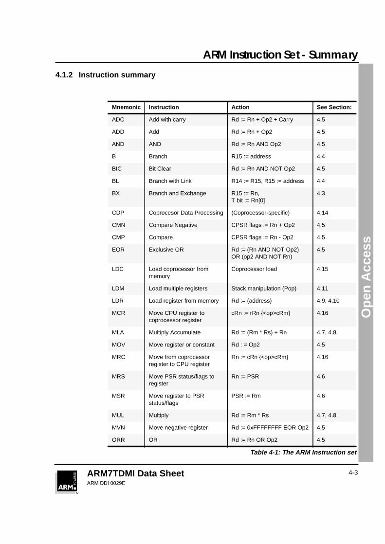
4.1.2 Instruction summary
Mnemonic Instruction Action See Section:
ADC Add with carry Rd := Rn + Op2 + Carry 4.5
ADD Add Rd := Rn + Op2 4.5
AND AND Rd := Rn AND Op2 4.5
B Branch R15 := address 4.4
BIC Bit Clear Rd := Rn AND NOT Op2 4.5
BL Branch with Link R14 := R15, R15 := address 4.4
BX Branch and Exchange R15 := Rn,T bit := Rn[0]
4.3
CDP Coprocesor Data Processing (Coprocessor-specific) 4.14
CMN Compare Negative CPSR flags := Rn + Op2 4.5
CMP Compare CPSR flags := Rn - Op2 4.5
EOR Exclusive OR Rd := (Rn AND NOT Op2)OR (op2 AND NOT Rn)
4.5
LDC Load coprocessor frommemory
Coprocessor load 4.15
LDM Load multiple registers Stack manipulation (Pop) 4.11
LDR Load register from memory Rd := (address) 4.9, 4.10
MCR Move CPU register tocoprocessor register
cRn := rRn {<op>cRm} 4.16
MLA Multiply Accumulate Rd := (Rm * Rs) + Rn 4.7, 4.8
MOV Move register or constant Rd : = Op2 4.5
MRC Move from coprocessorregister to CPU register
Rn := cRn {<op>cRm} 4.16
MRS Move PSR status/flags toregister
Rn := PSR 4.6
MSR Move register to PSRstatus/flags
PSR := Rm 4.6
MUL Multiply Rd := Rm * Rs 4.7, 4.8
MVN Move negative register Rd := 0xFFFFFFFF EOR Op2 4.5
ORR OR Rd := Rn OR Op2 4.5
Table 4-1: The ARM Instruction set
ARM Instruction Set - Summary
ARM7TDMI Data SheetARM DDI 0029E
4-4
Ope
n A
cces
s
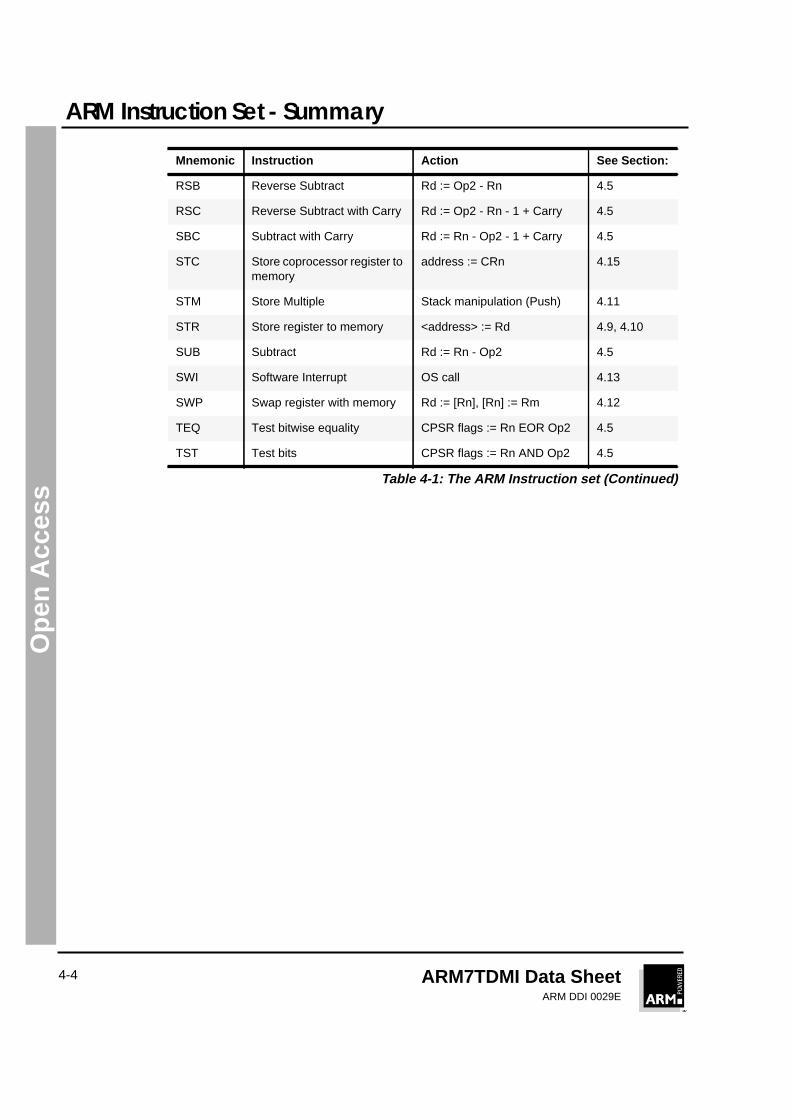
RSB Reverse Subtract Rd := Op2 - Rn 4.5
RSC Reverse Subtract with Carry Rd := Op2 - Rn - 1 + Carry 4.5
SBC Subtract with Carry Rd := Rn - Op2 - 1 + Carry 4.5
STC Store coprocessor register tomemory
address := CRn 4.15
STM Store Multiple Stack manipulation (Push) 4.11
STR Store register to memory <address> := Rd 4.9, 4.10
SUB Subtract Rd := Rn - Op2 4.5
SWI Software Interrupt OS call 4.13
SWP Swap register with memory Rd := [Rn], [Rn] := Rm 4.12
TEQ Test bitwise equality CPSR flags := Rn EOR Op2 4.5
TST Test bits CPSR flags := Rn AND Op2 4.5
Mnemonic Instruction Action See Section:
Table 4-1: The ARM Instruction set (Continued)
ARM Instruction Set - Condition Field
ARM7TDMI Data SheetARM DDI 0029E
4-5
Ope
n A
cces
s
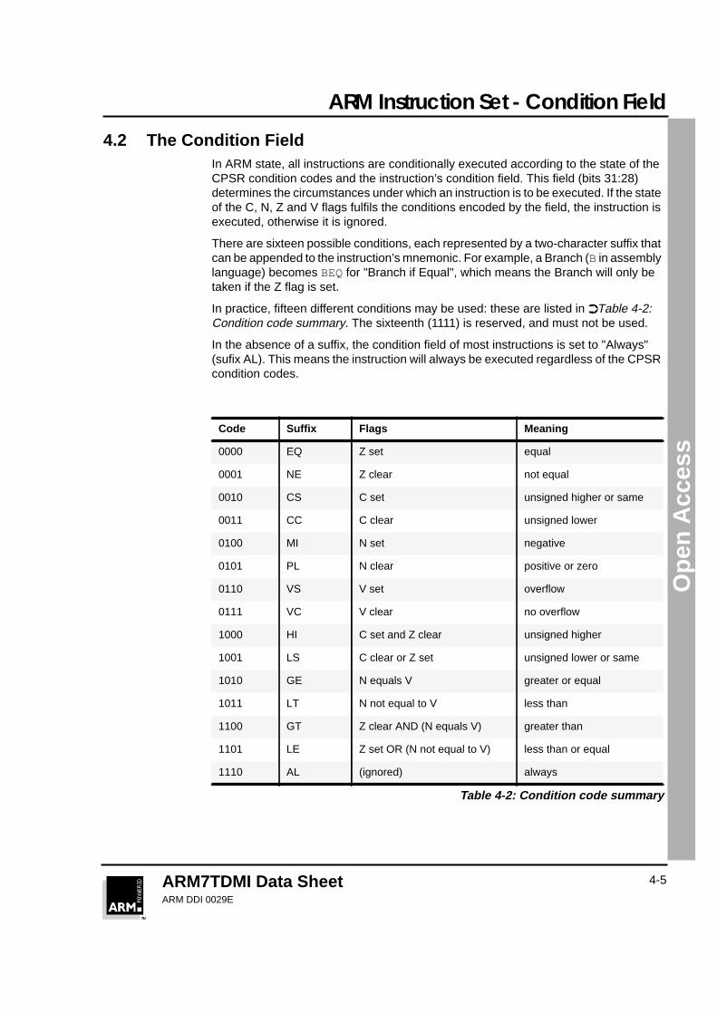
4.2 The Condition FieldIn ARM state, all instructions are conditionally executed according to the state of theCPSR condition codes and the instruction’s condition field. This field (bits 31:28)determines the circumstances under which an instruction is to be executed. If the stateof the C, N, Z and V flags fulfils the conditions encoded by the field, the instruction isexecuted, otherwise it is ignored.
There are sixteen possible conditions, each represented by a two-character suffix thatcan be appended to the instruction’s mnemonic. For example, a Branch (B in assemblylanguage) becomes BEQ for "Branch if Equal", which means the Branch will only betaken if the Z flag is set.
In practice, fifteen different conditions may be used: these are listed in ➲Table 4-2:Condition code summary. The sixteenth (1111) is reserved, and must not be used.
In the absence of a suffix, the condition field of most instructions is set to "Always"(sufix AL). This means the instruction will always be executed regardless of the CPSRcondition codes.
Code Suffix Flags Meaning
0000 EQ Z set equal
0001 NE Z clear not equal
0010 CS C set unsigned higher or same
0011 CC C clear unsigned lower
0100 MI N set negative
0101 PL N clear positive or zero
0110 VS V set overflow
0111 VC V clear no overflow
1000 HI C set and Z clear unsigned higher
1001 LS C clear or Z set unsigned lower or same
1010 GE N equals V greater or equal
1011 LT N not equal to V less than
1100 GT Z clear AND (N equals V) greater than
1101 LE Z set OR (N not equal to V) less than or equal
1110 AL (ignored) always
Table 4-2: Condition code summary
ARM Instruction Set - Condition Field
ARM7TDMI Data SheetARM DDI 0029E
4-6
Ope
n A
cces
s
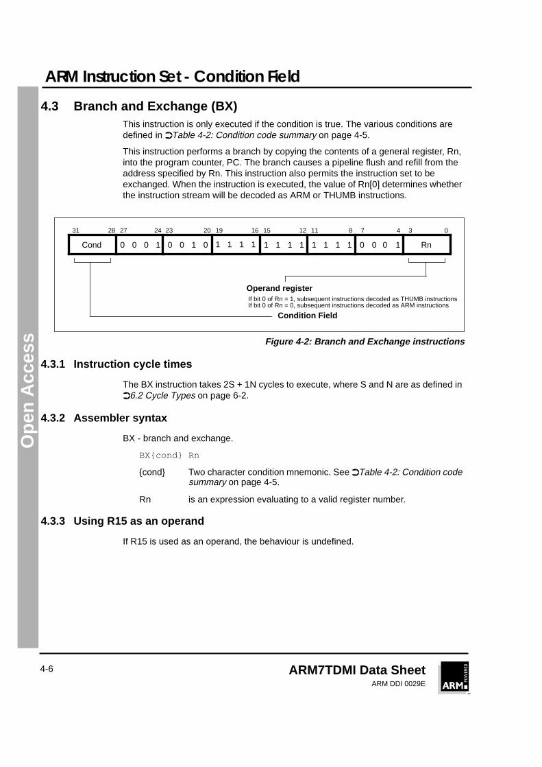
4.3 Branch and Exchange (BX)This instruction is only executed if the condition is true. The various conditions aredefined in ➲Table 4-2: Condition code summary on page 4-5.
This instruction performs a branch by copying the contents of a general register, Rn,into the program counter, PC. The branch causes a pipeline flush and refill from theaddress specified by Rn. This instruction also permits the instruction set to beexchanged. When the instruction is executed, the value of Rn[0] determines whetherthe instruction stream will be decoded as ARM or THUMB instructions.
Figure 4-2: Branch and Exchange instructions
4.3.1 Instruction cycle times
The BX instruction takes 2S + 1N cycles to execute, where S and N are as defined in➲6.2 Cycle Types on page 6-2.
4.3.2 Assembler syntax
BX - branch and exchange.
BX{cond} Rn
{cond} Two character condition mnemonic. See ➲Table 4-2: Condition codesummary on page 4-5.
Rn is an expression evaluating to a valid register number.
4.3.3 Using R15 as an operand
If R15 is used as an operand, the behaviour is undefined.
Cond 0 0 0 1 0 0 1 0 0 0 0 1 Rn
034781112151619202324272831
Operand registerIf bit 0 of Rn = 1, subsequent instructions decoded as THUMB instructionsIf bit 0 of Rn = 0, subsequent instructions decoded as ARM instructions
Condition Field
1 1 1 1 1 1 1 1 1 1 1 1
ARM Instruction Set - Condition Field
ARM7TDMI Data SheetARM DDI 0029E
4-7
Ope
n A
cces
s
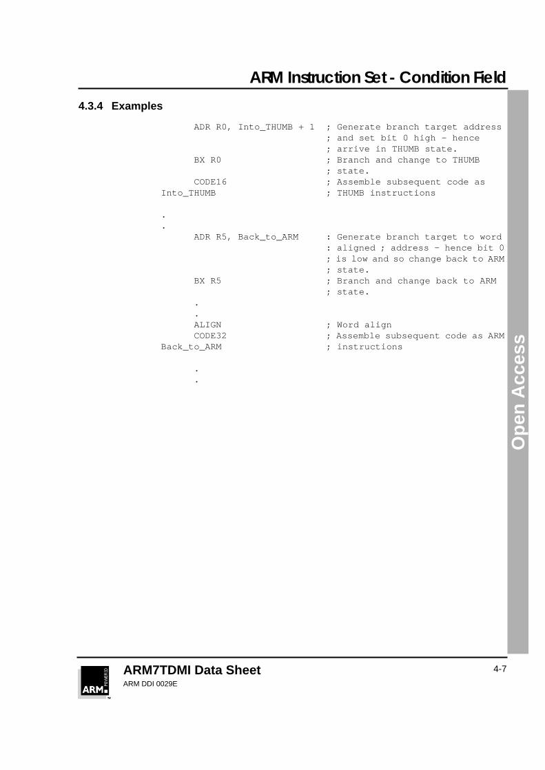
4.3.4 Examples
ADR R0, Into_THUMB + 1 ; Generate branch target address; and set bit 0 high - hence; arrive in THUMB state.
BX R0 ; Branch and change to THUMB; state.
CODE16 ; Assemble subsequent code asInto_THUMB ; THUMB instructions
.
.ADR R5, Back_to_ARM : Generate branch target to word
: aligned ; address - hence bit 0; is low and so change back to ARM; state.
BX R5 ; Branch and change back to ARM; state.
.
.ALIGN ; Word alignCODE32 ; Assemble subsequent code as ARM
Back_to_ARM ; instructions
.
.
ARM Instruction Set - B, BL
ARM7TDMI Data SheetARM DDI 0029E
4-8
Ope
n A
cces
s
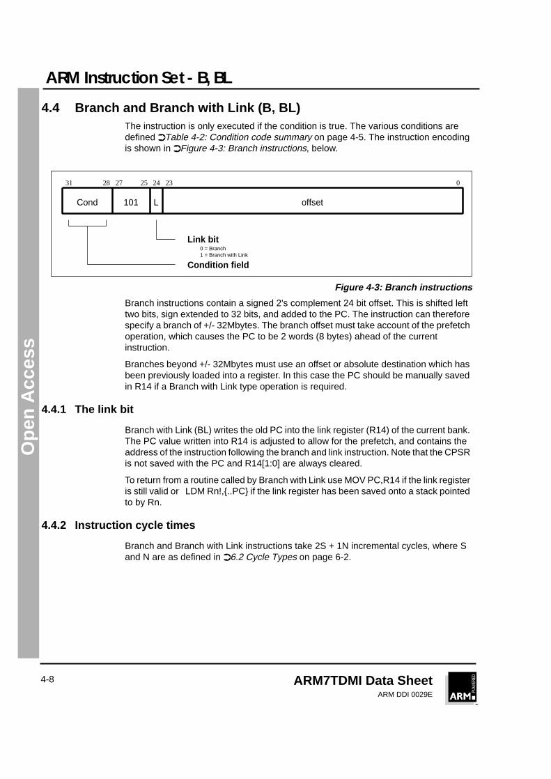
4.4 Branch and Branch with Link (B, BL)The instruction is only executed if the condition is true. The various conditions aredefined ➲Table 4-2: Condition code summary on page 4-5. The instruction encodingis shown in ➲Figure 4-3: Branch instructions, below.
Figure 4-3: Branch instructions
Branch instructions contain a signed 2's complement 24 bit offset. This is shifted lefttwo bits, sign extended to 32 bits, and added to the PC. The instruction can thereforespecify a branch of +/- 32Mbytes. The branch offset must take account of the prefetchoperation, which causes the PC to be 2 words (8 bytes) ahead of the currentinstruction.
Branches beyond +/- 32Mbytes must use an offset or absolute destination which hasbeen previously loaded into a register. In this case the PC should be manually savedin R14 if a Branch with Link type operation is required.
4.4.1 The link bit
Branch with Link (BL) writes the old PC into the link register (R14) of the current bank.The PC value written into R14 is adjusted to allow for the prefetch, and contains theaddress of the instruction following the branch and link instruction. Note that the CPSRis not saved with the PC and R14[1:0] are always cleared.
To return from a routine called by Branch with Link use MOV PC,R14 if the link registeris still valid or LDM Rn!,{..PC} if the link register has been saved onto a stack pointedto by Rn.
4.4.2 Instruction cycle times
Branch and Branch with Link instructions take 2S + 1N incremental cycles, where Sand N are as defined in ➲6.2 Cycle Types on page 6-2.
Cond 101 L offset
31 28 27 25 24 23 0
Link bit0 = Branch1 = Branch with Link
Condition field
ARM Instruction Set - B, BL
ARM7TDMI Data SheetARM DDI 0029E
4-9
Ope
n A
cces
s
4.4.3 Assembler syntax
Items in {} are optional. Items in <> must be present.
B{L}{cond} <expression>
{L} is used to request the Branch with Link form of the instruction.If absent, R14 will not be affected by the instruction.
{cond} is a two-character mnemonic as shown in ➲Table 4-2:Condition code summary on page 4-5. If absent then AL(ALways) will be used.
<expression> is the destination. The assembler calculates the offset.
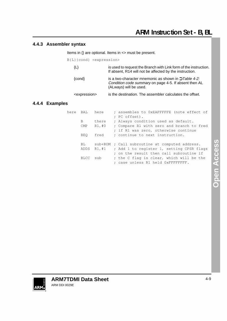
4.4.4 Examples
here BAL here ; assembles to 0xEAFFFFFE (note effect of; PC offset).
B there ; Always condition used as default.CMP R1,#0 ; Compare R1 with zero and branch to fred
; if R1 was zero, otherwise continueBEQ fred ; continue to next instruction.
BL sub+ROM ; Call subroutine at computed address.ADDS R1,#1 ; Add 1 to register 1, setting CPSR flags
; on the result then call subroutine ifBLCC sub ; the C flag is clear, which will be the
; case unless R1 held 0xFFFFFFFF.
ARM Instruction Set - Data processing
ARM7TDMI Data SheetARM DDI 0029E
4-10
Ope
n A
cces
s
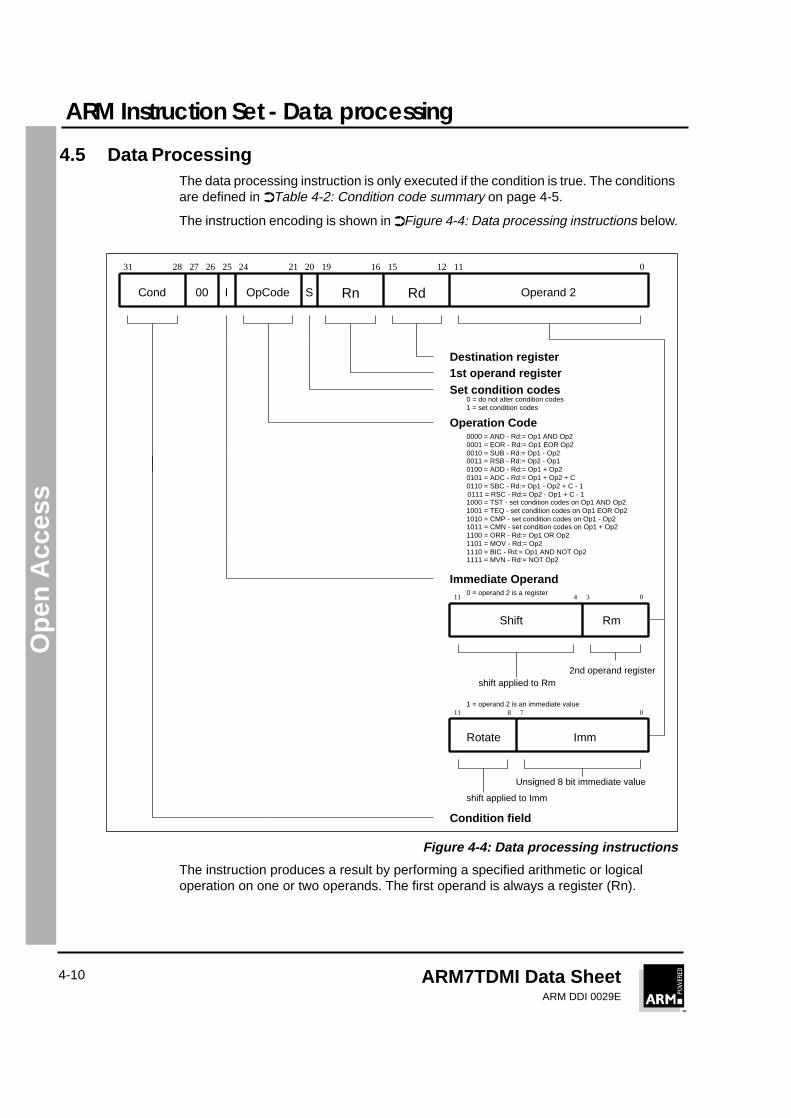
4.5 Data ProcessingThe data processing instruction is only executed if the condition is true. The conditionsare defined in ➲Table 4-2: Condition code summary on page 4-5.
The instruction encoding is shown in ➲Figure 4-4: Data processing instructions below.
Figure 4-4: Data processing instructions
The instruction produces a result by performing a specified arithmetic or logicaloperation on one or two operands. The first operand is always a register (Rn).
Cond 00 I OpCode Rn Rd Operand 2
011121516192021242526272831
Destination register1st operand registerSet condition codes
Operation Code
0 = do not alter condition codes1 = set condition codes
0000 = AND - Rd:= Op1 AND Op2
0010 = SUB - Rd:= Op1 - Op20011 = RSB - Rd:= Op2 - Op10100 = ADD - Rd:= Op1 + Op20101 = ADC - Rd:= Op1 + Op2 + C0110 = SBC - Rd:= Op1 - Op2 + C0111 = RSC - Rd:= Op2 - Op1 + C1000 = TST - set condition codes on Op1 AND Op21001 = TEQ - set condition codes on Op1 EOR Op21010 = CMP - set condition codes on Op1 - Op21011 = CMN - set condition codes on Op1 + Op21100 = ORR - Rd:= Op1 OR Op21101 = MOV - Rd:= Op21110 = BIC - Rd:= Op1 AND NOT Op21111 = MVN - Rd:= NOT Op2
Immediate Operand0 = operand 2 is a register
1 = operand 2 is an immediate value
Shift Rm
Rotate
S
Unsigned 8 bit immediate value
2nd operand registershift applied to Rm
shift applied to Imm
Imm
Condition field
11 8 7 0
03411
0001 = EOR - Rd:= Op1 EOR Op2
- 1- 1
ARM Instruction Set - Data processing
ARM7TDMI Data SheetARM DDI 0029E
4-11
Ope
n A
cces
s
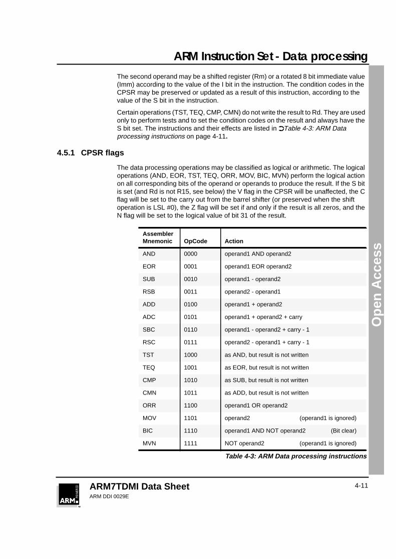
The second operand may be a shifted register (Rm) or a rotated 8 bit immediate value(Imm) according to the value of the I bit in the instruction. The condition codes in theCPSR may be preserved or updated as a result of this instruction, according to thevalue of the S bit in the instruction.
Certain operations (TST, TEQ, CMP, CMN) do not write the result to Rd. They are usedonly to perform tests and to set the condition codes on the result and always have theS bit set. The instructions and their effects are listed in ➲Table 4-3: ARM Dataprocessing instructions on page 4-11.
4.5.1 CPSR flags
The data processing operations may be classified as logical or arithmetic. The logicaloperations (AND, EOR, TST, TEQ, ORR, MOV, BIC, MVN) perform the logical actionon all corresponding bits of the operand or operands to produce the result. If the S bitis set (and Rd is not R15, see below) the V flag in the CPSR will be unaffected, the Cflag will be set to the carry out from the barrel shifter (or preserved when the shiftoperation is LSL #0), the Z flag will be set if and only if the result is all zeros, and theN flag will be set to the logical value of bit 31 of the result.
AssemblerMnemonic OpCode Action
AND 0000 operand1 AND operand2
EOR 0001 operand1 EOR operand2
SUB 0010 operand1 - operand2
RSB 0011 operand2 - operand1
ADD 0100 operand1 + operand2
ADC 0101 operand1 + operand2 + carry
SBC 0110 operand1 - operand2 + carry - 1
RSC 0111 operand2 - operand1 + carry - 1
TST 1000 as AND, but result is not written
TEQ 1001 as EOR, but result is not written
CMP 1010 as SUB, but result is not written
CMN 1011 as ADD, but result is not written
ORR 1100 operand1 OR operand2
MOV 1101 operand2 (operand1 is ignored)
BIC 1110 operand1 AND NOT operand2 (Bit clear)
MVN 1111 NOT operand2 (operand1 is ignored)
Table 4-3: ARM Data processing instructions
ARM Instruction Set - Shifts
ARM7TDMI Data SheetARM DDI 0029E
4-12
Ope
n A
cces
s
The arithmetic operations (SUB, RSB, ADD, ADC, SBC, RSC, CMP, CMN) treat eachoperand as a 32 bit integer (either unsigned or 2's complement signed, the two areequivalent). If the S bit is set (and Rd is not R15) the V flag in the CPSR will be set ifan overflow occurs into bit 31 of the result; this may be ignored if the operands wereconsidered unsigned, but warns of a possible error if the operands were 2'scomplement signed. The C flag will be set to the carry out of bit 31 of the ALU, the Zflag will be set if and only if the result was zero, and the N flag will be set to the valueof bit 31 of the result (indicating a negative result if the operands are considered to be2's complement signed).
4.5.2 Shifts
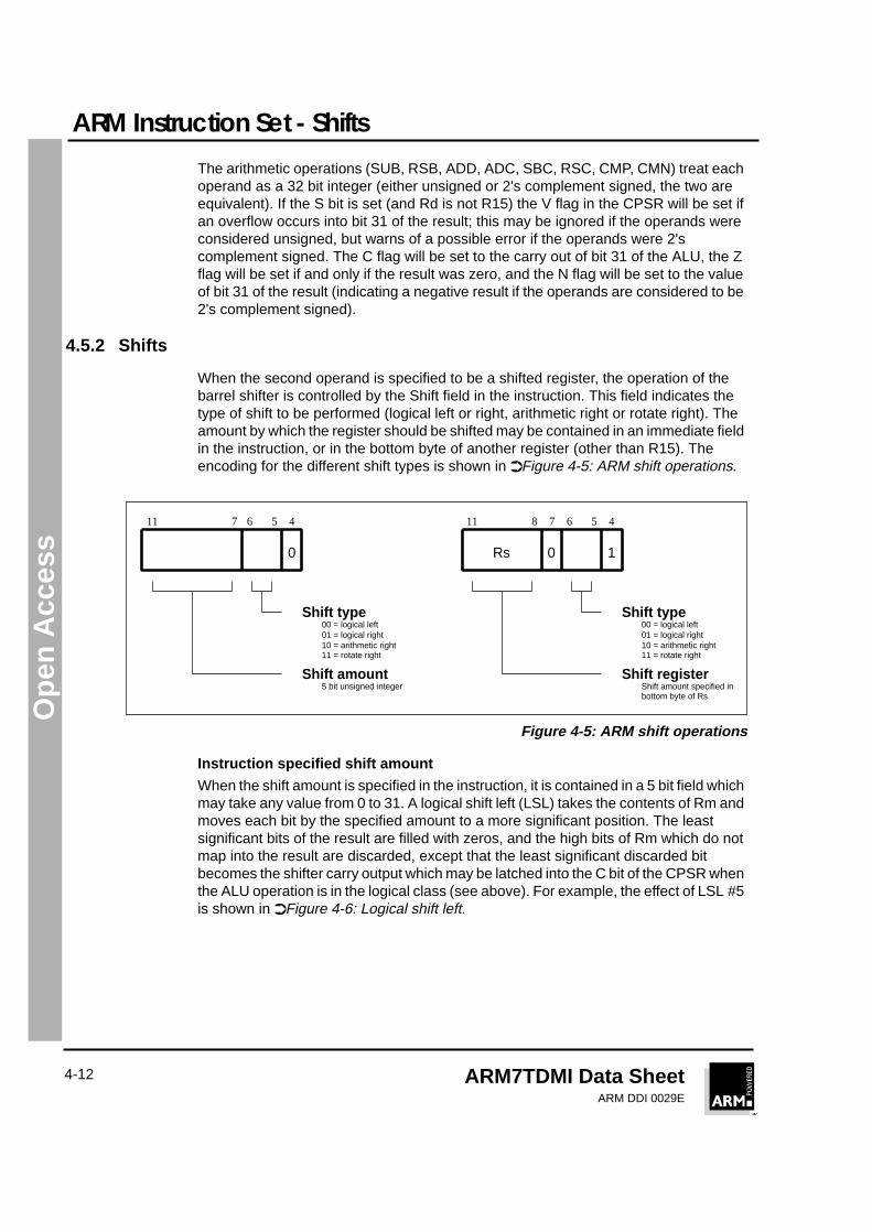
When the second operand is specified to be a shifted register, the operation of thebarrel shifter is controlled by the Shift field in the instruction. This field indicates thetype of shift to be performed (logical left or right, arithmetic right or rotate right). Theamount by which the register should be shifted may be contained in an immediate fieldin the instruction, or in the bottom byte of another register (other than R15). Theencoding for the different shift types is shown in ➲Figure 4-5: ARM shift operations.
Figure 4-5: ARM shift operations
Instruction specified shift amount
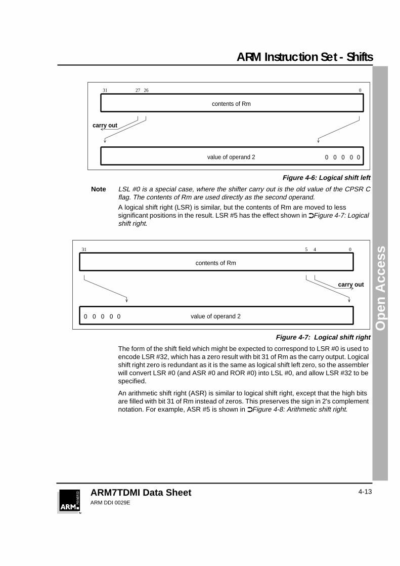
When the shift amount is specified in the instruction, it is contained in a 5 bit field whichmay take any value from 0 to 31. A logical shift left (LSL) takes the contents of Rm andmoves each bit by the specified amount to a more significant position. The leastsignificant bits of the result are filled with zeros, and the high bits of Rm which do notmap into the result are discarded, except that the least significant discarded bitbecomes the shifter carry output which may be latched into the C bit of the CPSR whenthe ALU operation is in the logical class (see above). For example, the effect of LSL #5is shown in ➲Figure 4-6: Logical shift left.
0 0 1Rs
11 8 7 6 5 411 7 6 5 4
Shift type
Shift amount5 bit unsigned integer
00 = logical left01 = logical right10 = arithmetic right11 = rotate right
Shift type
Shift register
00 = logical left01 = logical right10 = arithmetic right11 = rotate right
Shift amount specified inbottom byte of Rs
ARM Instruction Set - Shifts
ARM7TDMI Data SheetARM DDI 0029E
4-13
Ope
n A
cces
s
Figure 4-6: Logical shift left
Note LSL #0 is a special case, where the shifter carry out is the old value of the CPSR Cflag. The contents of Rm are used directly as the second operand.
A logical shift right (LSR) is similar, but the contents of Rm are moved to lesssignificant positions in the result. LSR #5 has the effect shown in ➲Figure 4-7: Logicalshift right.
Figure 4-7: Logical shift right
The form of the shift field which might be expected to correspond to LSR #0 is used toencode LSR #32, which has a zero result with bit 31 of Rm as the carry output. Logicalshift right zero is redundant as it is the same as logical shift left zero, so the assemblerwill convert LSR #0 (and ASR #0 and ROR #0) into LSL #0, and allow LSR #32 to bespecified.
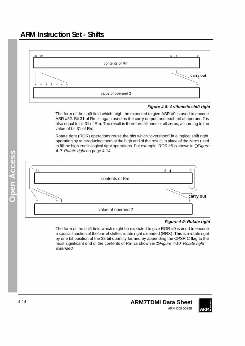
An arithmetic shift right (ASR) is similar to logical shift right, except that the high bitsare filled with bit 31 of Rm instead of zeros. This preserves the sign in 2's complementnotation. For example, ASR #5 is shown in ➲Figure 4-8: Arithmetic shift right.
0 0 0 0 0
contents of Rm
value of operand 2
31 27 26 0
carry out
contents of Rm
value of operand 2
31 0
carry out
0 0 0 0 0
5 4
ARM Instruction Set - Shifts
ARM7TDMI Data SheetARM DDI 0029E
4-14
Ope
n A
cces
s
Figure 4-8: Arithmetic shift right
The form of the shift field which might be expected to give ASR #0 is used to encodeASR #32. Bit 31 of Rm is again used as the carry output, and each bit of operand 2 isalso equal to bit 31 of Rm. The result is therefore all ones or all zeros, according to thevalue of bit 31 of Rm.
Rotate right (ROR) operations reuse the bits which “overshoot” in a logical shift rightoperation by reintroducing them at the high end of the result, in place of the zeros usedto fill the high end in logical right operations. For example, ROR #5 is shown in ➲Figure4-9: Rotate right on page 4-14.
Figure 4-9: Rotate right
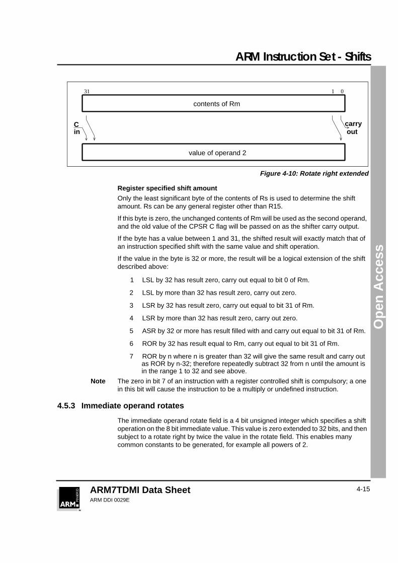
The form of the shift field which might be expected to give ROR #0 is used to encodea special function of the barrel shifter, rotate right extended (RRX). This is a rotate rightby one bit position of the 33 bit quantity formed by appending the CPSR C flag to themost significant end of the contents of Rm as shown in ➲Figure 4-10: Rotate rightextended.
contents of Rm
value of operand 2
31 0
carry out
5 430
contents of Rm
value of operand 2
31 0
carry out
5 4
ARM Instruction Set - Shifts
ARM7TDMI Data SheetARM DDI 0029E
4-15
Ope
n A
cces
s
Figure 4-10: Rotate right extended
Register specified shift amount
Only the least significant byte of the contents of Rs is used to determine the shiftamount. Rs can be any general register other than R15.
If this byte is zero, the unchanged contents of Rm will be used as the second operand,and the old value of the CPSR C flag will be passed on as the shifter carry output.
If the byte has a value between 1 and 31, the shifted result will exactly match that ofan instruction specified shift with the same value and shift operation.
If the value in the byte is 32 or more, the result will be a logical extension of the shiftdescribed above:
1 LSL by 32 has result zero, carry out equal to bit 0 of Rm.
2 LSL by more than 32 has result zero, carry out zero.
3 LSR by 32 has result zero, carry out equal to bit 31 of Rm.
4 LSR by more than 32 has result zero, carry out zero.
5 ASR by 32 or more has result filled with and carry out equal to bit 31 of Rm.
6 ROR by 32 has result equal to Rm, carry out equal to bit 31 of Rm.
7 ROR by n where n is greater than 32 will give the same result and carry outas ROR by n-32; therefore repeatedly subtract 32 from n until the amount isin the range 1 to 32 and see above.
Note The zero in bit 7 of an instruction with a register controlled shift is compulsory; a onein this bit will cause the instruction to be a multiply or undefined instruction.
4.5.3 Immediate operand rotates
The immediate operand rotate field is a 4 bit unsigned integer which specifies a shiftoperation on the 8 bit immediate value. This value is zero extended to 32 bits, and thensubject to a rotate right by twice the value in the rotate field. This enables manycommon constants to be generated, for example all powers of 2.
contents of Rm
value of operand 2
31 0
carryout
1
Cin
ARM Instruction Set - TEQ, TST, CMP & CMN
ARM7TDMI Data SheetARM DDI 0029E
4-16
Ope
n A
cces
s
4.5.4 Writing to R15
When Rd is a register other than R15, the condition code flags in the CPSR may beupdated from the ALU flags as described above.
When Rd is R15 and the S flag in the instruction is not set the result of the operationis placed in R15 and the CPSR is unaffected.
When Rd is R15 and the S flag is set the result of the operation is placed in R15 andthe SPSR corresponding to the current mode is moved to the CPSR. This allows statechanges which atomically restore both PC and CPSR. This form of instruction shouldnot be used in User mode.
4.5.5 Using R15 as an operand
If R15 (the PC) is used as an operand in a data processing instruction the register isused directly.
The PC value will be the address of the instruction, plus 8 or 12 bytes due to instructionprefetching. If the shift amount is specified in the instruction, the PC will be 8 bytesahead. If a register is used to specify the shift amount the PC will be 12 bytes ahead.
4.5.6 TEQ, TST, CMP and CMN opcodes
Note TEQ, TST, CMP and CMN do not write the result of their operation but do set flags inthe CPSR. An assembler should always set the S flag for these instructions even if thisis not specified in the mnemonic.
The TEQP form of the TEQ instruction used in earlier ARM processors must not beused: the PSR transfer operations should be used instead.
The action of TEQP in the ARM7TDMI is to move SPSR_<mode> to the CPSR if theprocessor is in a privileged mode and to do nothing if in User mode.
4.5.7 Instruction cycle times
Data Processing instructions vary in the number of incremental cycles taken asfollows:
S, N and I are as defined in ➲6.2 Cycle Types on page 6-2.
Processing Type Cycles
Normal Data Processing 1S
Data Processing with register specified shift 1S + 1I
Data Processing with PC written 2S + 1N
Data Processing with register specified shift and PC written 2S + 1N + 1I
Table 4-4: Incremental cycle times
ARM Instruction Set - TEQ, TST, CMP & CMN
ARM7TDMI Data SheetARM DDI 0029E
4-17
Ope
n A
cces
s
4.5.8 Assembler syntax
1 MOV,MVN (single operand instructions.)
<opcode>{cond}{S} Rd,<Op2>
2 CMP,CMN,TEQ,TST (instructions which do not produce a result.)
<opcode>{cond} Rn,<Op2>
3 AND,EOR,SUB,RSB,ADD,ADC,SBC,RSC,ORR,BIC
<opcode>{cond}{S} Rd,Rn,<Op2>
where:
<Op2> is Rm{,<shift>} or,<#expression>
{cond} is a two-character condition mnemonic. See ➲Table 4-2:Condition code summary on page 4-5.
{S} set condition codes if S present (implied for CMP, CMN, TEQ,TST).
Rd, Rn and Rm are expressions evaluating to a register number.
<#expression> if this is used, the assembler will attempt to generate a shiftedimmediate 8-bit field to match the expression. If this isimpossible, it will give an error.
<shift> is <shiftname> <register> or <shiftname> #expression, orRRX (rotate right one bit with extend).
<shiftname>s are: ASL, LSL, LSR, ASR, ROR. (ASL is a synonym for LSL,they assemble to the same code.)
4.5.9 Examples
ADDEQ R2,R4,R5 ; If the Z flag is set make R2:=R4+R5TEQS R4,#3 ; test R4 for equality with 3.
; (The S is in fact redundant as the ; assembler inserts it automatically.)
SUB R4,R5,R7,LSR R2 ; Logical right shift R7 by the number in ; the bottom byte of R2, subtract result ; from R5, and put the answer into R4.
MOV PC,R14 ; Return from subroutine.MOVS PC,R14 ; Return from exception and restore CPSR
; from SPSR_mode.
ARM Instruction Set - MRS, MSR
ARM7TDMI Data SheetARM DDI 0029E
4-18
Ope
n A
cces
s
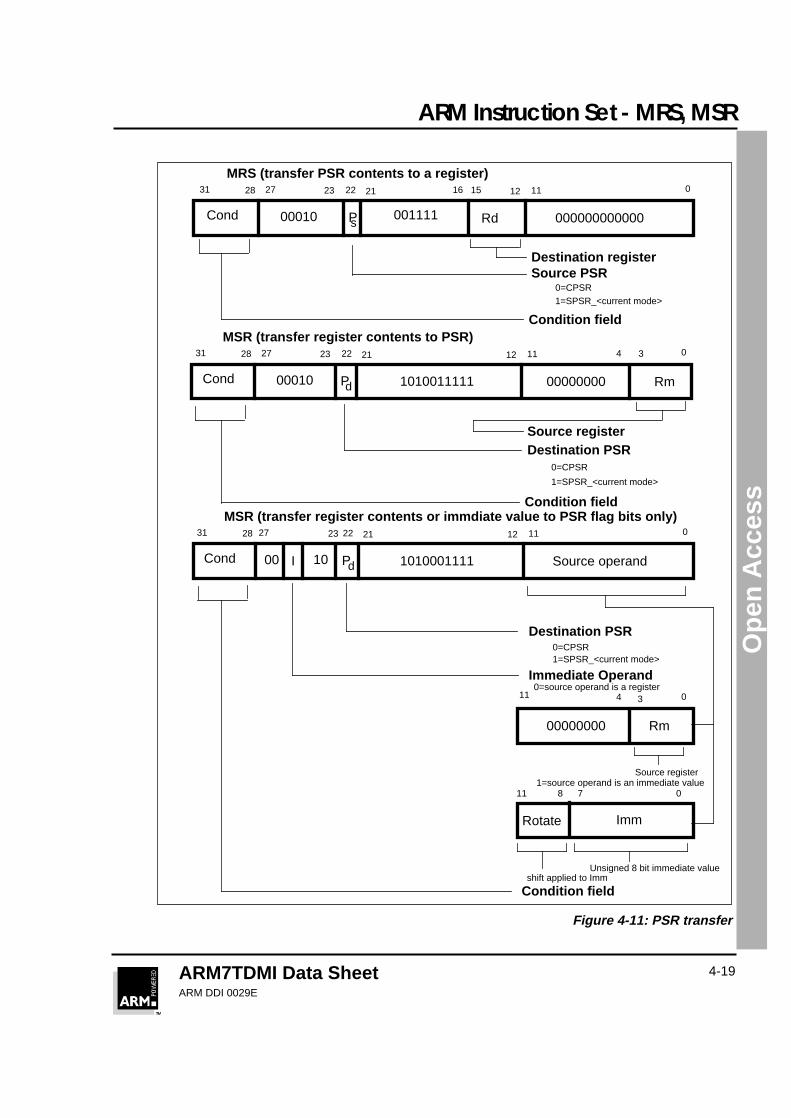
4.6 PSR Transfer (MRS, MSR)The instruction is only executed if the condition is true. The various conditions aredefined in ➲Table 4-2: Condition code summary on page 4-5.
The MRS and MSR instructions are formed from a subset of the Data Processingoperations and are implemented using the TEQ, TST, CMN and CMP instructionswithout the S flag set. The encoding is shown in ➲Figure 4-11: PSR transfer on page4-19.
These instructions allow access to the CPSR and SPSR registers. The MRSinstruction allows the contents of the CPSR or SPSR_<mode> to be moved to ageneral register. The MSR instruction allows the contents of a general register to bemoved to the CPSR or SPSR_<mode> register.
The MSR instruction also allows an immediate value or register contents to betransferred to the condition code flags (N,Z,C and V) of CPSR or SPSR_<mode>without affecting the control bits. In this case, the top four bits of the specified registercontents or 32 bit immediate value are written to the top four bits of the relevant PSR.
4.6.1 Operand restrictions
• In User mode, the control bits of the CPSR are protected from change, so onlythe condition code flags of the CPSR can be changed. In other (privileged)modes the entire CPSR can be changed.Note that the software must never change the state of the T bit in the CPSR.If this happens, the processor will enter an unpredictable state.
• The SPSR register which is accessed depends on the mode at the time ofexecution. For example, only SPSR_fiq is accessible when the processor is inFIQ mode.
• You must not specify R15 as the source or destination register.
• Also, do not attempt to access an SPSR in User mode, since no such registerexists.
ARM Instruction Set - MRS, MSR
ARM7TDMI Data SheetARM DDI 0029E
4-19
Ope
n A
cces
s
Figure 4-11: PSR transfer
Cond
0
000000000000RdP00010 s001111
16 15 12 112228 2131 2327
MRS (transfer PSR contents to a register)
Destination registerSource PSR
Condition field
0=CPSR1=SPSR_<current mode>
Cond
0
00000000 RmP00010 d 1010011111
4 312 112228 2131 2327
MSR (transfer register contents to PSR)
Source registerDestination PSR
Condition field
0=CPSR
1=SPSR_<current mode>
Cond
0
Source operandP00 d 1010001111
12 112228 2131 2327
MSR (transfer register contents or immdiate value to PSR flag bits only)
Destination PSR
Immediate Operand
0=CPSR1=SPSR_<current mode>
I 10
11 4 3 00=source operand is a register
1=source operand is an immediate value11 8 7 0
Condition field
00000000
Rotate Imm
Rm
Source register
Unsigned 8 bit immediate valueshift applied to Imm
ARM Instruction Set - MRS, MSR
ARM7TDMI Data SheetARM DDI 0029E
4-20
Ope
n A
cces
s
4.6.2 Reserved bits
Only twelve bits of the PSR are defined in ARM7TDMI (N,Z,C,V,I,F, T & M[4:0]); theremaining bits are reserved for use in future versions of the processor. Refer to➲Figure 3-6: Program status register format on page 3-8 for a full description of thePSR bits.
To ensure the maximum compatibility between ARM7TDMI programs and futureprocessors, the following rules should be observed:
• The reserved bits should be preserved when changing the value in a PSR.
• Programs should not rely on specific values from the reserved bits whenchecking the PSR status, since they may read as one or zero in futureprocessors.
A read-modify-write strategy should therefore be used when altering the control bits ofany PSR register; this involves transferring the appropriate PSR register to a generalregister using the MRS instruction, changing only the relevant bits and thentransferring the modified value back to the PSR register using the MSR instruction.
Example
The following sequence performs a mode change:
MRS R0,CPSR ; Take a copy of the CPSR.BIC R0,R0,#0x1F ; Clear the mode bits.ORR R0,R0,#new_mode ; Select new modeMSR CPSR,R0 ; Write back the modified
; CPSR.
When the aim is simply to change the condition code flags in a PSR, a value can bewritten directly to the flag bits without disturbing the control bits. The followinginstruction sets the N,Z,C and V flags:
MSR CPSR_flg,#0xF0000000 ; Set all the flags; regardless of their; previous state (does not; affect any control bits).
No attempt should be made to write an 8 bit immediate value into the whole PSR sincesuch an operation cannot preserve the reserved bits.
4.6.3 Instruction cycle times
PSR Transfers take 1S incremental cycles, where S is as defined in ➲6.2 Cycle Typeson page 6-2.
ARM Instruction Set - MRS, MSR
ARM7TDMI Data SheetARM DDI 0029E
4-21
Ope
n A
cces
s
4.6.4 Assembler syntax
1 MRS - transfer PSR contents to a register
MRS{cond} Rd,<psr>
2 MSR - transfer register contents to PSR
MSR{cond} <psr>,Rm
3 MSR - transfer register contents to PSR flag bits only
MSR{cond} <psrf>,Rm
The most significant four bits of the register contents are written to the N,Z,C& V flags respectively.
4 MSR - transfer immediate value to PSR flag bits only
MSR{cond} <psrf>,<#expression>
The expression should symbolise a 32 bit value of which the most significantfour bits are written to the N,Z,C and V flags respectively.
Key:
{cond} two-character condition mnemonic. See ➲Table 4-2:Condition code summary on page 4-5.
Rd and Rm are expressions evaluating to a register number other thanR15
<psr> is CPSR, CPSR_all, SPSR or SPSR_all. (CPSR andCPSR_all are synonyms as are SPSR and SPSR_all)
<psrf> is CPSR_flg or SPSR_flg
<#expression> where this is used, the assembler will attempt to generate ashifted immediate 8-bit field to match the expression. If this isimpossible, it will give an error.
ARM Instruction Set - MRS, MSR
ARM7TDMI Data SheetARM DDI 0029E
4-22
Ope
n A
cces
s
4.6.5 Examples
In User mode the instructions behave as follows:
MSR CPSR_all,Rm ; CPSR[31:28] <- Rm[31:28]MSR CPSR_flg,Rm ; CPSR[31:28] <- Rm[31:28]MSR CPSR_flg,#0xA0000000 ; CPSR[31:28] <- 0xA
;(set N,C; clear Z,V)MRS Rd,CPSR ; Rd[31:0] <- CPSR[31:0]
In privileged modes the instructions behave as follows:
MSR CPSR_all,Rm ; CPSR[31:0] <- Rm[31:0]MSR CPSR_flg,Rm ; CPSR[31:28] <- Rm[31:28]MSR CPSR_flg,#0x50000000 ; CPSR[31:28] <- 0x5
;(set Z,V; clear N,C)MRS Rd,CPSR ; Rd[31:0] <- CPSR[31:0]MSR SPSR_all,Rm ;SPSR_<mode>[31:0]<- Rm[31:0]MSR SPSR_flg,Rm ; SPSR_<mode>[31:28] <- Rm[31:28]MSR SPSR_flg,#0xC0000000 ; SPSR_<mode>[31:28] <- 0xC
;(set N,Z; clear C,V)MRS Rd,SPSR ; Rd[31:0] <- SPSR_<mode>[31:0]
ARM Instruction Set - MUL, MLA
ARM7TDMI Data SheetARM DDI 0029E
4-23
Ope
n A
cces
s
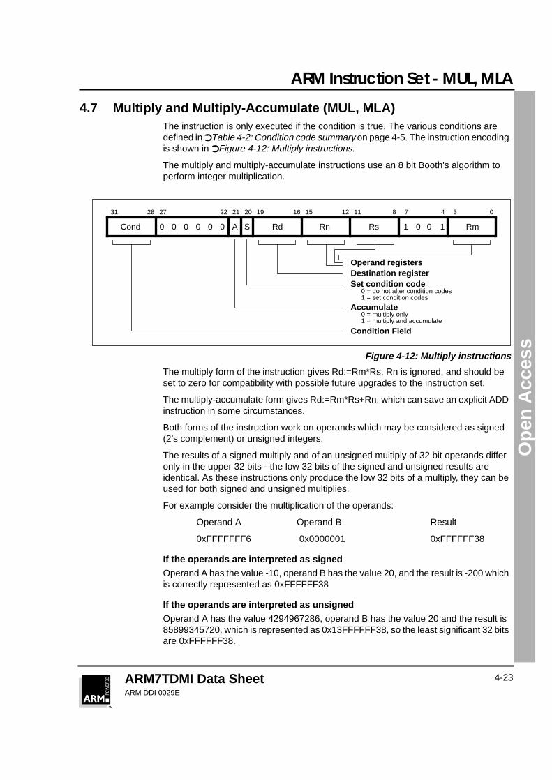
4.7 Multiply and Multiply-Accumulate (MUL, MLA)The instruction is only executed if the condition is true. The various conditions aredefined in ➲Table 4-2: Condition code summary on page 4-5. The instruction encodingis shown in ➲Figure 4-12: Multiply instructions.
The multiply and multiply-accumulate instructions use an 8 bit Booth's algorithm toperform integer multiplication.
Figure 4-12: Multiply instructions
The multiply form of the instruction gives Rd:=Rm*Rs. Rn is ignored, and should beset to zero for compatibility with possible future upgrades to the instruction set.
The multiply-accumulate form gives Rd:=Rm*Rs+Rn, which can save an explicit ADDinstruction in some circumstances.
Both forms of the instruction work on operands which may be considered as signed(2’s complement) or unsigned integers.
The results of a signed multiply and of an unsigned multiply of 32 bit operands differonly in the upper 32 bits - the low 32 bits of the signed and unsigned results areidentical. As these instructions only produce the low 32 bits of a multiply, they can beused for both signed and unsigned multiplies.
For example consider the multiplication of the operands:
Operand A Operand B Result
0xFFFFFFF6 0x0000001 0xFFFFFF38
If the operands are interpreted as signed
Operand A has the value -10, operand B has the value 20, and the result is -200 whichis correctly represented as 0xFFFFFF38
If the operands are interpreted as unsigned
Operand A has the value 4294967286, operand B has the value 20 and the result is85899345720, which is represented as 0x13FFFFFF38, so the least significant 32 bitsare 0xFFFFFF38.
Cond 0 0 0 0 0 0 A S Rd Rn Rs 1 0 0 1 Rm
034781112151619202122272831
Operand registersDestination registerSet condition code
Accumulate
0 = do not alter condition codes1 = set condition codes
0 = multiply only1 = multiply and accumulate
Condition Field
ARM Instruction Set - MUL, MLA
ARM7TDMI Data SheetARM DDI 0029E
4-24
Ope
n A
cces
s
4.7.1 Operand restrictions
The destination register Rd must not be the same as the operand register Rm. R15must not be used as an operand or as the destination register.
All other register combinations will give correct results, and Rd, Rn and Rs may usethe same register when required.
4.7.2 CPSR flags
Setting the CPSR flags is optional, and is controlled by the S bit in the instruction. TheN (Negative) and Z (Zero) flags are set correctly on the result (N is made equal to bit31 of the result, and Z is set if and only if the result is zero). The C (Carry) flag is setto a meaningless value and the V (oVerflow) flag is unaffected.
4.7.3 Instruction cycle times
MUL takes 1S + mI and MLA 1S + (m+1)I cycles to execute, where S and I are asdefined in ➲6.2 Cycle Types on page 6-2.
m is the number of 8 bit multiplier array cycles required to complete themultiply, which is controlled by the value of the multiplier operandspecified by Rs. Its possible values are as follows
1 if bits [32:8] of the multiplier operand are all zero or all one.2 if bits [32:16] of the multiplier operand are all zero or all one.3 if bits [32:24] of the multiplier operand are all zero or all one.4 in all other cases.
4.7.4 Assembler syntax
MUL{cond}{S} Rd,Rm,Rs
MLA{cond}{S} Rd,Rm,Rs,Rn
{cond} two-character condition mnemonic. See ➲Table 4-2:Condition code summary on page 4-5.
{S} set condition codes if S present
Rd, Rm, Rs and Rn are expressions evaluating to a register number otherthan R15.
4.7.5 Examples
MUL R1,R2,R3 ; R1:=R2*R3MLAEQS R1,R2,R3,R4 ; Conditionally R1:=R2*R3+R4,
; setting condition codes.
ARM Instruction Set - MULL,MLAL
ARM7TDMI Data SheetARM DDI 0029E
4-25
Ope
n A
cces
s
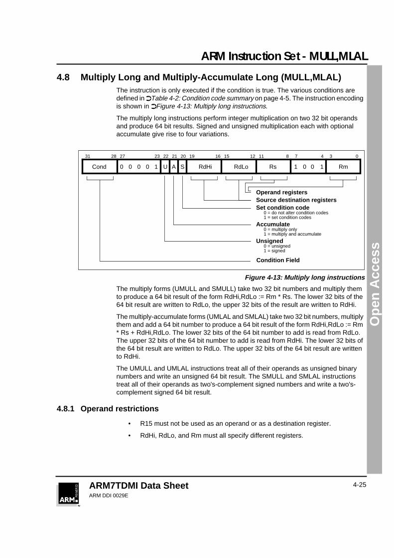
4.8 Multiply Long and Multiply-Accumulate Long (MULL,MLAL)The instruction is only executed if the condition is true. The various conditions aredefined in ➲Table 4-2: Condition code summary on page 4-5. The instruction encodingis shown in ➲Figure 4-13: Multiply long instructions.
The multiply long instructions perform integer multiplication on two 32 bit operandsand produce 64 bit results. Signed and unsigned multiplication each with optionalaccumulate give rise to four variations.
Figure 4-13: Multiply long instructions
The multiply forms (UMULL and SMULL) take two 32 bit numbers and multiply themto produce a 64 bit result of the form RdHi,RdLo := Rm * Rs. The lower 32 bits of the64 bit result are written to RdLo, the upper 32 bits of the result are written to RdHi.
The multiply-accumulate forms (UMLAL and SMLAL) take two 32 bit numbers, multiplythem and add a 64 bit number to produce a 64 bit result of the form RdHi,RdLo := Rm* Rs + RdHi,RdLo. The lower 32 bits of the 64 bit number to add is read from RdLo.The upper 32 bits of the 64 bit number to add is read from RdHi. The lower 32 bits ofthe 64 bit result are written to RdLo. The upper 32 bits of the 64 bit result are writtento RdHi.
The UMULL and UMLAL instructions treat all of their operands as unsigned binarynumbers and write an unsigned 64 bit result. The SMULL and SMLAL instructionstreat all of their operands as two's-complement signed numbers and write a two's-complement signed 64 bit result.
4.8.1 Operand restrictions
• R15 must not be used as an operand or as a destination register.
• RdHi, RdLo, and Rm must all specify different registers.
Cond 0 0 0 0 1 U A S RdHi RdLo Rs 1 0 0 1 Rm
03478111215161920212223272831
Operand registersSource destination registersSet condition code
Accumulate
Unsigned
0 = do not alter condition codes1 = set condition codes
0 = multiply only1 = multiply and accumulate
0 = unsigned1 = signed
Condition Field
ARM Instruction Set - MULL,MLAL
ARM7TDMI Data SheetARM DDI 0029E
4-26
Ope
n A
cces
s
4.8.2 CPSR flags
Setting the CPSR flags is optional, and is controlled by the S bit in the instruction. TheN and Z flags are set correctly on the result (N is equal to bit 63 of the result, Z is setif and only if all 64 bits of the result are zero). Both the C and V flags are set tomeaningless values.
4.8.3 Instruction cycle times
MULL takes 1S + (m+1)I and MLAL 1S + (m+2)I cycles to execute, where m is thenumber of 8 bit multiplier array cycles required to complete the multiply, which iscontrolled by the value of the multiplier operand specified by Rs.
Its possible values are as follows:
For signed instructions SMULL, SMLAL:
1 if bits [31:8] of the multiplier operand are all zero or all one.2 if bits [31:16] of the multiplier operand are all zero or all one.3 if bits [31:24] of the multiplier operand are all zero or all one.4 in all other cases.
For unsigned instructions UMULL, UMLAL:
1 if bits [31:8] of the multiplier operand are all zero.2 if bits [31:16] of the multiplier operand are all zero.3 if bits [31:24] of the multiplier operand are all zero.4 in all other cases.
S and I are as defined in ➲6.2 Cycle Types on page 6-2.
4.8.4 Assembler syntax
Mnemonic Description Purpose
UMULL{cond}{S} RdLo,RdHi,Rm,Rs Unsigned Multiply Long 32 x 32 = 64
UMLAL{cond}{S} RdLo,RdHi,Rm,Rs Unsigned Multiply & Accumulate Long 32 x 32 + 64 = 64
SMULL{cond}{S} RdLo,RdHi,Rm,Rs Signed Multiply Long 32 x 32 = 64
SMLAL{cond}{S} RdLo,RdHi,Rm,Rs Signed Multiply & Accumulate Long 32 x 32 + 64 = 64
Table 4-5: Assembler syntax descriptions
ARM Instruction Set - MULL,MLAL
ARM7TDMI Data SheetARM DDI 0029E
4-27
Ope
n A
cces
s
where:
{cond} two-character condition mnemonic. See ➲Table 4-2:Condition code summary on page 4-5.
{S} set condition codes if S present
RdLo, RdHi, Rm, Rs are expressions evaluating to a register number otherthan R15.
4.8.5 Examples
UMULL R1,R4,R2,R3 ; R4,R1:=R2*R3UMLALS R1,R5,R2,R3 ; R5,R1:=R2*R3+R5,R1 also setting
; condition codes
ARM Instruction Set - LDR, STR
ARM7TDMI Data SheetARM DDI 0029E
4-28
Ope
n A
cces
s
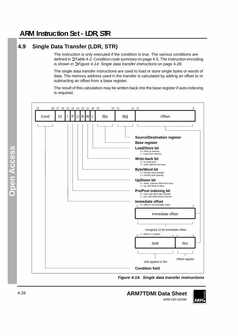
4.9 Single Data Transfer (LDR, STR)The instruction is only executed if the condition is true. The various conditions aredefined in ➲Table 4-2: Condition code summary on page 4-5. The instruction encodingis shown in ➲Figure 4-14: Single data transfer instructions on page 4-28.
The single data transfer instructions are used to load or store single bytes or words ofdata. The memory address used in the transfer is calculated by adding an offset to orsubtracting an offset from a base register.
The result of this calculation may be written back into the base register if auto-indexingis required.
Figure 4-14: Single data transfer instructions
Cond I Rn Rd
011121516192021242526272831
01 P U B W L Offset
2223
011
Source/Destination registerBase registerLoad/Store bit
0 = Store to memory1 = Load from memory
Write-back bit
Byte/Word bit
0 = no write-back1 = write address into base
0 = transfer word quantity1 = transfer byte quantity
Up/Down bit
Pre/Post indexing bit
0 = offset is an immediate valueImmediate offset
Immediate offset
Unsigned 12 bit immediate offset1 = offset is a register
11 0
shift applied to Rm
34
Condition field
0 = down; subtract offset from base1 = up; add offset to base
0 = post; add offset after transfer1 = pre; add offset before transfer
Offset register
Shift Rm
ARM Instruction Set - LDR, STR
ARM7TDMI Data SheetARM DDI 0029E
4-29
Ope
n A
cces
s
4.9.1 Offsets and auto-indexing
The offset from the base may be either a 12 bit unsigned binary immediate value inthe instruction, or a second register (possibly shifted in some way). The offset may beadded to (U=1) or subtracted from (U=0) the base register Rn. The offset modificationmay be performed either before (pre-indexed, P=1) or after (post-indexed, P=0) thebase is used as the transfer address.
The W bit gives optional auto increment and decrement addressing modes. Themodified base value may be written back into the base (W=1), or the old base valuemay be kept (W=0). In the case of post-indexed addressing, the write back bit isredundant and is always set to zero, since the old base value can be retained bysetting the offset to zero. Therefore post-indexed data transfers always write back themodified base. The only use of the W bit in a post-indexed data transfer is in privilegedmode code, where setting the W bit forces non-privileged mode for the transfer,allowing the operating system to generate a user address in a system where thememory management hardware makes suitable use of this hardware.
4.9.2 Shifted register offset
The 8 shift control bits are described in the data processing instructions section.However, the register specified shift amounts are not available in this instruction class.See ➲4.5.2 Shifts on page 4-12.
4.9.3 Bytes and words
This instruction class may be used to transfer a byte (B=1) or a word (B=0) betweenan ARM7TDMI register and memory.
The action of LDR(B) and STR(B) instructions is influenced by the BIGEND controlsignal. The two possible configurations are described below.
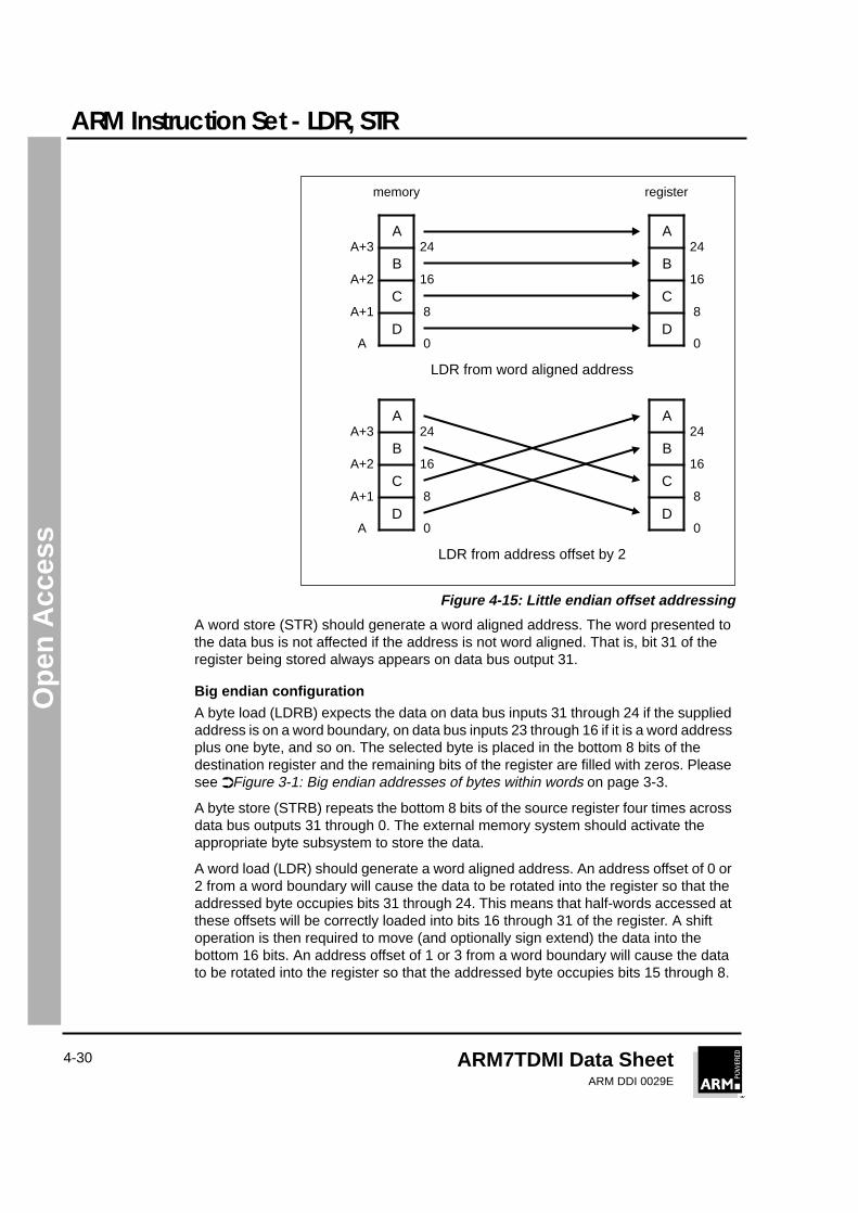
Little endian configuration
A byte load (LDRB) expects the data on data bus inputs 7 through 0 if the suppliedaddress is on a word boundary, on data bus inputs 15 through 8 if it is a word addressplus one byte, and so on. The selected byte is placed in the bottom 8 bits of thedestination register, and the remaining bits of the register are filled with zeros. Pleasesee ➲Figure 3-2: Little endian addresses of bytes within words on page 3-3.
A byte store (STRB) repeats the bottom 8 bits of the source register four times acrossdata bus outputs 31 through 0. The external memory system should activate theappropriate byte subsystem to store the data.
A word load (LDR) will normally use a word aligned address. However, an addressoffset from a word boundary will cause the data to be rotated into the register so thatthe addressed byte occupies bits 0 to 7. This means that half-words accessed atoffsets 0 and 2 from the word boundary will be correctly loaded into bits 0 through 15of the register. Two shift operations are then required to clear or to sign extend theupper 16 bits. This is illustrated in ➲Figure 4-15: Little endian offset addressing onpage 4-30.
ARM Instruction Set - LDR, STR
ARM7TDMI Data SheetARM DDI 0029E
4-30
Ope
n A
cces
s
Figure 4-15: Little endian offset addressing
A word store (STR) should generate a word aligned address. The word presented tothe data bus is not affected if the address is not word aligned. That is, bit 31 of theregister being stored always appears on data bus output 31.
Big endian configuration
A byte load (LDRB) expects the data on data bus inputs 31 through 24 if the suppliedaddress is on a word boundary, on data bus inputs 23 through 16 if it is a word addressplus one byte, and so on. The selected byte is placed in the bottom 8 bits of thedestination register and the remaining bits of the register are filled with zeros. Pleasesee ➲Figure 3-1: Big endian addresses of bytes within words on page 3-3.
A byte store (STRB) repeats the bottom 8 bits of the source register four times acrossdata bus outputs 31 through 0. The external memory system should activate theappropriate byte subsystem to store the data.
A word load (LDR) should generate a word aligned address. An address offset of 0 or2 from a word boundary will cause the data to be rotated into the register so that theaddressed byte occupies bits 31 through 24. This means that half-words accessed atthese offsets will be correctly loaded into bits 16 through 31 of the register. A shiftoperation is then required to move (and optionally sign extend) the data into thebottom 16 bits. An address offset of 1 or 3 from a word boundary will cause the datato be rotated into the register so that the addressed byte occupies bits 15 through 8.
A
B
C
D
memory
A+3
A+2
A+1
A
24
16
8
0
A
B
C
D
register
24
16
8
0
LDR from word aligned address
A
B
C
D
A+3
A+2
A+1
A
24
16
8
0
A
B
C
D
24
16
8
0
LDR from address offset by 2
ARM Instruction Set - LDR, STR
ARM7TDMI Data SheetARM DDI 0029E
4-31
Ope
n A
cces
s
A word store (STR) should generate a word aligned address. The word presented tothe data bus is not affected if the address is not word aligned. That is, bit 31 of theregister being stored always appears on data bus output 31.
4.9.4 Use of R15
Write-back must not be specified if R15 is specified as the base register (Rn). Whenusing R15 as the base register you must remember it contains an address 8 bytes onfrom the address of the current instruction.
R15 must not be specified as the register offset (Rm).
When R15 is the source register (Rd) of a register store (STR) instruction, the storedvalue will be address of the instruction plus 12.
4.9.5 Restriction on the use of base register
When configured for late aborts, the following example code is difficult to unwind asthe base register, Rn, gets updated before the abort handler starts. Sometimes it maybe impossible to calculate the initial value.
After an abort, the following example code is difficult to unwind as the base register,Rn, gets updated before the abort handler starts. Sometimes it may be impossible tocalculate the initial value.
Example:
LDR R0,[R1],R1
Therefore a post-indexed LDR or STR where Rm is the same register as Rn shouldnot be used.
4.9.6 Data aborts
A transfer to or from a legal address may cause problems for a memory managementsystem. For instance, in a system which uses virtual memory the required data maybe absent from main memory. The memory manager can signal a problem by takingthe processor ABORT input HIGH whereupon the Data Abort trap will be taken. It isup to the system software to resolve the cause of the problem, then the instruction canbe restarted and the original program continued.
4.9.7 Instruction cycle times
Normal LDR instructions take 1S + 1N + 1I and LDR PC take 2S + 2N +1I incrementalcycles, where S,N and I are as defined in ➲6.2 Cycle Types on page 6-2.
STR instructions take 2N incremental cycles to execute.
ARM Instruction Set - LDR, STR
ARM7TDMI Data SheetARM DDI 0029E
4-32
Ope
n A
cces
s
4.9.8 Assembler syntax
<LDR|STR>{cond}{B}{T} Rd,<Address>
where:
LDR load from memory into a register
STR store from a register into memory
{cond} two-character condition mnemonic. See ➲Table 4-2: Condition codesummary on page 4-5.
{B} if B is present then byte transfer, otherwise word transfer
{T} if T is present the W bit will be set in a post-indexed instruction, forcingnon-privileged mode for the transfer cycle. T is not allowed when apre-indexed addressing mode is specified or implied.
Rd is an expression evaluating to a valid register number.
Rn and Rm are expressions evaluating to a register number. If Rn is R15 then theassembler will subtract 8 from the offset value to allow for ARM7TDMIpipelining. In this case base write-back should not be specified.
<Address> can be:
1 An expression which generates an address:
<expression>
The assembler will attempt to generate an instruction usingthe PC as a base and a corrected immediate offset to addressthe location given by evaluating the expression. This will be aPC relative, pre-indexed address. If the address is out ofrange, an error will be generated.
2 A pre-indexed addressing specification:
[Rn] offset of zero
[Rn,<#expression>]{!} offset of <expression>bytes
[Rn,{+/-}Rm{,<shift>}]{!} offset of +/- contents ofindex register, shiftedby <shift>
3 A post-indexed addressing specification:
[Rn],<#expression> offset of <expression>bytes
[Rn],{+/-}Rm{,<shift>} offset of +/- contents ofindex register, shiftedas by <shift>.
ARM Instruction Set - LDR, STR
ARM7TDMI Data SheetARM DDI 0029E
4-33
Ope
n A
cces
s
<shift> general shift operation (see data processing instructions) butyou cannot specify the shift amount by a register.
{!} writes back the base register (set the W bit) if! is present.
4.9.9 Examples
STR R1,[R2,R4]! ; Store R1 at R2+R4 (both of which are; registers) and write back address to; R2.
STR R1,[R2],R4 ; Store R1 at R2 and write back; R2+R4 to R2.
LDR R1,[R2,#16] ; Load R1 from contents of R2+16, but; don't write back.
LDR R1,[R2,R3,LSL#2] ; Load R1 from contents of R2+R3*4.LDREQBR1,[R6,#5] ; Conditionally load byte at R6+5 into
; R1 bits 0 to 7, filling bits 8 to 31; with zeros.
STR R1,PLACE ; Generate PC relative offset to; address PLACE.
•PLACE
ARM Instruction Set - LDR, STR
ARM7TDMI Data SheetARM DDI 0029E
4-34
Ope
n A
cces
s
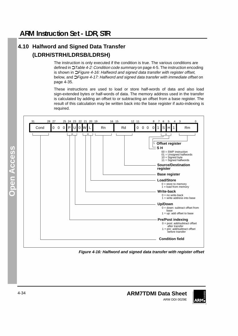
4.10 Halfword and Signed Data Transfer
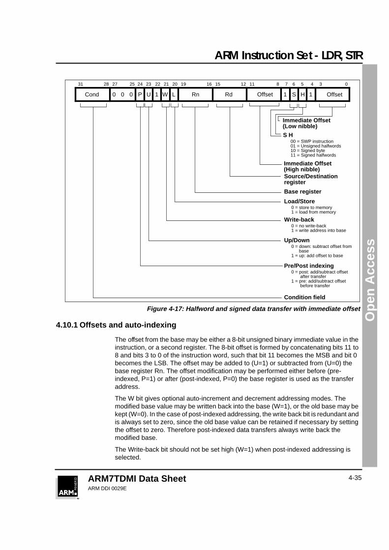
(LDRH/STRH/LDRSB/LDRSH)The instruction is only executed if the condition is true. The various conditions aredefined in ➲Table 4-2: Condition code summary on page 4-5. The instruction encodingis shown in ➲Figure 4-16: Halfword and signed data transfer with register offset,below, and ➲Figure 4-17: Halfword and signed data transfer with immediate offset onpage 4-35.
These instructions are used to load or store half-words of data and also loadsign-extended bytes or half-words of data. The memory address used in the transferis calculated by adding an offset to or subtracting an offset from a base register. Theresult of this calculation may be written back into the base register if auto-indexing isrequired.
Figure 4-16: Halfword and signed data transfer with register offset
Cond 0 0 0 P U 0 W L Rn Rd 0 0 0 0 Rm
034781112151619202122272831
Offset register
Base register
S H
Source/Destination
00 = SWP instruction01 = Unsigned halfwords
0 = store to memory1 = load from memory
Load/Store
1 S H 1
10 = Signed byte11 = Signed halfwords
register
0 = no write-back1 = write address into base
Write-back
0 = down: subtract offset frombase
Up/Down
1 = up: add offset to base
0 = post: add/subtract offsetPre/Post indexing
after transfer1 = pre: add/subtract offset
before transfer
Condition field
232425 56
ARM Instruction Set - LDR, STR
ARM7TDMI Data SheetARM DDI 0029E
4-35
Ope
n A
cces
s
Figure 4-17: Halfword and signed data transfer with immediate offset
4.10.1 Offsets and auto-indexing
The offset from the base may be either a 8-bit unsigned binary immediate value in theinstruction, or a second register. The 8-bit offset is formed by concatenating bits 11 to8 and bits 3 to 0 of the instruction word, such that bit 11 becomes the MSB and bit 0becomes the LSB. The offset may be added to (U=1) or subtracted from (U=0) thebase register Rn. The offset modification may be performed either before (pre-indexed, P=1) or after (post-indexed, P=0) the base register is used as the transferaddress.
The W bit gives optional auto-increment and decrement addressing modes. Themodified base value may be written back into the base (W=1), or the old base may bekept (W=0). In the case of post-indexed addressing, the write back bit is redundant andis always set to zero, since the old base value can be retained if necessary by settingthe offset to zero. Therefore post-indexed data transfers always write back themodified base.
The Write-back bit should not be set high (W=1) when post-indexed addressing isselected.
Cond 0 0 0 P U 1 W L Rn Rd Offset
034781112151619202122272831
Immediate Offset
Base register
S H
Source/Destination
00 = SWP instruction01 = Unsigned halfwords
0 = store to memory1 = load from memory
Load/Store
1 S H 1
10 = Signed byte11 = Signed halfwords
register
0 = no write-back1 = write address into base
Write-back
0 = down: subtract offset frombase
Up/Down
1 = up: add offset to base
0 = post: add/subtract offsetPre/Post indexing
after transfer1 = pre: add/subtract offset
before transfer
Condition field
232425 56
Offset
Immediate Offset(High nibble)
(Low nibble)
ARM Instruction Set - LDR, STR
ARM7TDMI Data SheetARM DDI 0029E
4-36
Ope
n A
cces
s
4.10.2 Halfword load and stores
Setting S=0 and H=1 may be used to transfer unsigned Half-words between anARM7TDMI register and memory.
The action of LDRH and STRH instructions is influenced by the BIGEND controlsignal. The two possible configurations are described in the section below.
4.10.3 Signed byte and halfword loads
The S bit controls the loading of sign-extended data. When S=1 the H bit selectsbetween Bytes (H=0) and Half-words (H=1). The L bit should not be set low (Store)when Signed (S=1) operations have been selected.
The LDRSB instruction loads the selected Byte into bits 7 to 0 of the destinationregister and bits 31 to 8 of the destination register are set to the value of bit 7, the signbit.
The LDRSH instruction loads the selected Half-word into bits 15 to 0 of the destinationregister and bits 31 to 16 of the destination register are set to the value of bit 15, thesign bit.
The action of the LDRSB and LDRSH instructions is influenced by the BIGEND controlsignal. The two possible configurations are described in the following section.
4.10.4 Endianness and byte/halfword selection
Little endian configuration
A signed byte load (LDRSB) expects data on data bus inputs 7 through to 0 if thesupplied address is on a word boundary, on data bus inputs 15 through to 8 if it is aword address plus one byte, and so on. The selected byte is placed in the bottom 8 bitof the destination register, and the remaining bits of the register are filled with the signbit, bit 7 of the byte. Please see ➲Figure 3-2: Little endian addresses of bytes withinwords on page 3-3
A halfword load (LDRSH or LDRH) expects data on data bus inputs 15 through to 0 ifthe supplied address is on a word boundary and on data bus inputs 31 through to 16if it is a halfword boundary, (A[1]=1).The supplied address should always be on ahalfword boundary. If bit 0 of the supplied address is HIGH then the ARM7TDMI willload an unpredictable value. The selected halfword is placed in the bottom 16 bits ofthe destination register. For unsigned half-words (LDRH), the top 16 bits of the registerare filled with zeros and for signed half-words (LDRSH) the top 16 bits are filled withthe sign bit, bit 15 of the halfword.
A halfword store (STRH) repeats the bottom 16 bits of the source register twice acrossthe data bus outputs 31 through to 0. The external memory system should activate theappropriate halfword subsystem to store the data. Note that the address must behalfword aligned, if bit 0 of the address is HIGH this will cause unpredictablebehaviour.
ARM Instruction Set - LDR, STR
ARM7TDMI Data SheetARM DDI 0029E
4-37
Ope
n A
cces
s
Big endian configuration
A signed byte load (LDRSB) expects data on data bus inputs 31 through to 24 if thesupplied address is on a word boundary, on data bus inputs 23 through to 16 if it is aword address plus one byte, and so on. The selected byte is placed in the bottom 8 bitof the destination register, and the remaining bits of the register are filled with the signbit, bit 7 of the byte. Please see ➲Figure 3-1: Big endian addresses of bytes withinwords on page 3-3
A halfword load (LDRSH or LDRH) expects data on data bus inputs 31 through to 16if the supplied address is on a word boundary and on data bus inputs 15 through to 0if it is a halfword boundary, (A[1]=1). The supplied address should always be on ahalfword boundary. If bit 0 of the supplied address is HIGH then the ARM7TDMI willload an unpredictable value. The selected halfword is placed in the bottom 16 bits ofthe destination register. For unsigned half-words (LDRH), the top 16 bits of the registerare filled with zeros and for signed half-words (LDRSH) the top 16 bits are filled withthe sign bit, bit 15 of the halfword.
A halfword store (STRH) repeats the bottom 16 bits of the source register twice acrossthe data bus outputs 31 through to 0. The external memory system should activate theappropriate halfword subsystem to store the data. Note that the address must behalfword aligned, if bit 0 of the address is HIGH this will cause unpredictablebehaviour.
4.10.5 Use of R15
Write-back should not be specified if R15 is specified as the base register (Rn). Whenusing R15 as the base register you must remember it contains an address 8 bytes onfrom the address of the current instruction.
R15 should not be specified as the register offset (Rm).
When R15 is the source register (Rd) of a Half-word store (STRH) instruction, thestored address will be address of the instruction plus 12.
4.10.6 Data aborts
A transfer to or from a legal address may cause problems for a memory managementsystem. For instance, in a system which uses virtual memory the required data maybe absent from the main memory. The memory manager can signal a problem bytaking the processor ABORT input HIGH whereupon the Data Abort trap will be taken.It is up to the system software to resolve the cause of the problem, then the instructioncan be restarted and the original program continued.
4.10.7 Instruction cycle times
Normal LDR(H,SH,SB) instructions take 1S + 1N + 1I
LDR(H,SH,SB) PC take 2S + 2N + 1I incremental cycles.
S,N and I are defined in➲6.2 Cycle Types on page 6-2.
STRH instructions take 2N incremental cycles to execute.
ARM Instruction Set - LDR, STR
ARM7TDMI Data SheetARM DDI 0029E
4-38
Ope
n A
cces
s
4.10.8 Assembler syntax
<LDR|STR>{cond}<H|SH|SB> Rd,<address>
LDR load from memory into a register
STR Store from a register into memory
{cond} two-character condition mnemonic. See ➲Table 4-2: Condition codesummary on page 4-5.
H Transfer halfword quantity
SB Load sign extended byte (Only valid for LDR)
SH Load sign extended halfword (Only valid for LDR)
Rd is an expression evaluating to a valid register number.
<address> can be:
1 An expression which generates an address:
<expression>
The assembler will attempt to generate an instruction usingthe PC as a base and a corrected immediate offset to addressthe location given by evaluating the expression. This will be aPC relative, pre-indexed address. If the address is out ofrange, an error will be generated.
2 A pre-indexed addressing specification:
[Rn] offset of zero
[Rn,<#expression>]{!} offset of <expression> bytes
[Rn,{+/-}Rm]{!} offset of +/- contents ofindex register
3 A post-indexed addressing specification:
[Rn],<#expression> offset of <expression> bytes
[Rn],{+/-}Rm offset of +/- contents ofindex register.
Rn and Rm are expressions evaluating to a register number.If Rn is R15 then the assembler will subtract 8 from the offsetvalue to allow for ARM7TDMI pipelining. In this case basewrite-back should not be specified.
{!} writes back the base register (set the W bit) if ! is present.
ARM Instruction Set - LDR, STR
ARM7TDMI Data SheetARM DDI 0029E
4-39
Ope
n A
cces
s
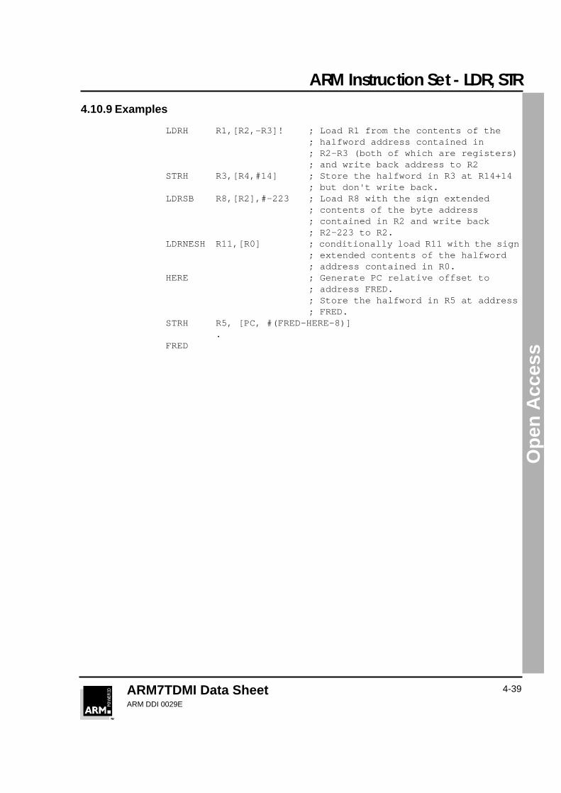
4.10.9 Examples
LDRH R1,[R2,-R3]! ; Load R1 from the contents of the; halfword address contained in; R2-R3 (both of which are registers); and write back address to R2
STRH R3,[R4,#14] ; Store the halfword in R3 at R14+14; but don't write back.
LDRSB R8,[R2],#-223 ; Load R8 with the sign extended; contents of the byte address; contained in R2 and write back; R2-223 to R2.
LDRNESH R11,[R0] ; conditionally load R11 with the sign; extended contents of the halfword; address contained in R0.
HERE ; Generate PC relative offset to; address FRED.; Store the halfword in R5 at address; FRED.
STRH R5, [PC, #(FRED-HERE-8)].
FRED
ARM Instruction Set - LDM, STM
ARM7TDMI Data SheetARM DDI 0029E
4-40
Ope
n A
cces
s
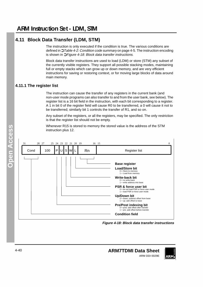
4.11 Block Data Transfer (LDM, STM)The instruction is only executed if the condition is true. The various conditions aredefined in ➲Table 4-2: Condition code summary on page 4-5. The instruction encodingis shown in ➲Figure 4-18: Block data transfer instructions.
Block data transfer instructions are used to load (LDM) or store (STM) any subset ofthe currently visible registers. They support all possible stacking modes, maintainingfull or empty stacks which can grow up or down memory, and are very efficientinstructions for saving or restoring context, or for moving large blocks of data aroundmain memory.
4.11.1 The register list
The instruction can cause the transfer of any registers in the current bank (andnon-user mode programs can also transfer to and from the user bank, see below). Theregister list is a 16 bit field in the instruction, with each bit corresponding to a register.A 1 in bit 0 of the register field will cause R0 to be transferred, a 0 will cause it not tobe transferred; similarly bit 1 controls the transfer of R1, and so on.
Any subset of the registers, or all the registers, may be specified. The only restrictionis that the register list should not be empty.
Whenever R15 is stored to memory the stored value is the address of the STMinstruction plus 12.
Figure 4-18: Block data transfer instructions
Cond Rn
015161920212425272831
P U W L
2223
100 S Register list
Base registerLoad/Store bit
0 = Store to memory1 = Load from memory
Write-back bit0 = no write-back1 = write address into base
Up/Down bit
Pre/Post indexing bit
0 = down; subtract offset from base1 = up; add offset to base
0 = post; add offset after transfer1 = pre; add offset before transfer
PSR & force user bit0 = do not load PSR or force user mode1 = load PSR or force user mode
Condition field
ARM Instruction Set - LDM, STM
ARM7TDMI Data SheetARM DDI 0029E
4-41
Ope
n A
cces
s
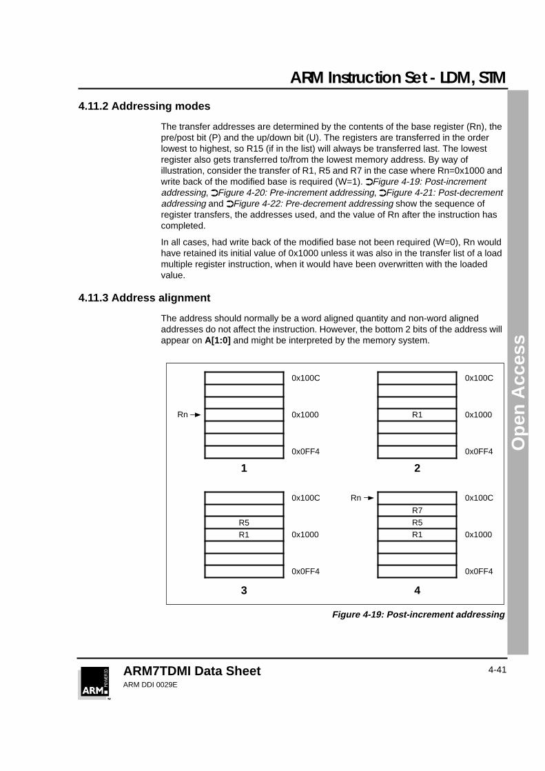
4.11.2 Addressing modes
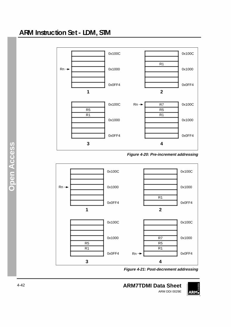
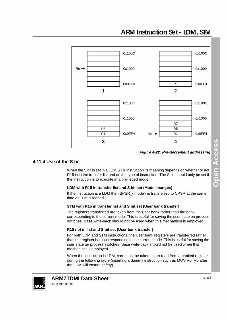
The transfer addresses are determined by the contents of the base register (Rn), thepre/post bit (P) and the up/down bit (U). The registers are transferred in the orderlowest to highest, so R15 (if in the list) will always be transferred last. The lowestregister also gets transferred to/from the lowest memory address. By way ofillustration, consider the transfer of R1, R5 and R7 in the case where Rn=0x1000 andwrite back of the modified base is required (W=1). ➲Figure 4-19: Post-incrementaddressing, ➲Figure 4-20: Pre-increment addressing, ➲Figure 4-21: Post-decrementaddressing and ➲Figure 4-22: Pre-decrement addressing show the sequence ofregister transfers, the addresses used, and the value of Rn after the instruction hascompleted.
In all cases, had write back of the modified base not been required (W=0), Rn wouldhave retained its initial value of 0x1000 unless it was also in the transfer list of a loadmultiple register instruction, when it would have been overwritten with the loadedvalue.
4.11.3 Address alignment
The address should normally be a word aligned quantity and non-word alignedaddresses do not affect the instruction. However, the bottom 2 bits of the address willappear on A[1:0] and might be interpreted by the memory system.
Figure 4-19: Post-increment addressing
0x100C
0x1000
0x0FF4
Rn
1
0x100C
0x1000
0x0FF4
2
R1
0x100C
0x1000
0x0FF4
3
0x100C
0x1000
0x0FF4
4
R1
R7
R5
R1
R5
Rn
ARM Instruction Set - LDM, STM
ARM7TDMI Data SheetARM DDI 0029E
4-42
Ope
n A
cces
s
Figure 4-20: Pre-increment addressing
Figure 4-21: Post-decrement addressing
0x100C
0x1000
0x0FF4
Rn
1
0x100C
0x1000
0x0FF4
2
R1
0x100C
0x1000
0x0FF4
3
0x100C
0x1000
0x0FF4
4
R1
R7
R5
R1
R5
Rn
0x100C
0x1000
0x0FF4
Rn
1
0x100C
0x1000
0x0FF4
2
R1
0x100C
0x1000
0x0FF4
3
0x100C
0x1000
0x0FF4
4
R1
R7
R5
R1
R5
Rn
ARM Instruction Set - LDM, STM
ARM7TDMI Data SheetARM DDI 0029E
4-43
Ope
n A
cces
s
Figure 4-22: Pre-decrement addressing
4.11.4 Use of the S bit
When the S bit is set in a LDM/STM instruction its meaning depends on whether or notR15 is in the transfer list and on the type of instruction. The S bit should only be set ifthe instruction is to execute in a privileged mode.
LDM with R15 in transfer list and S bit set (Mode changes)
If the instruction is a LDM then SPSR_<mode> is transferred to CPSR at the sametime as R15 is loaded.
STM with R15 in transfer list and S bit set (User bank transfer)
The registers transferred are taken from the User bank rather than the bankcorresponding to the current mode. This is useful for saving the user state on processswitches. Base write-back should not be used when this mechanism is employed.
R15 not in list and S bit set (User bank transfer)
For both LDM and STM instructions, the User bank registers are transferred ratherthan the register bank corresponding to the current mode. This is useful for saving theuser state on process switches. Base write-back should not be used when thismechanism is employed.
When the instruction is LDM, care must be taken not to read from a banked registerduring the following cycle (inserting a dummy instruction such as MOV R0, R0 afterthe LDM will ensure safety).
0x100C
0x1000
0x0FF4
Rn
1
0x100C
0x1000
0x0FF4
2
R1
0x100C
0x1000
0x0FF4
3
0x100C
0x1000
0x0FF4
4
R1
R7
R5
R1
R5
Rn
ARM Instruction Set - LDM, STM
ARM7TDMI Data SheetARM DDI 0029E
4-44
Ope
n A
cces
s
4.11.5 Use of R15 as the base
R15 should not be used as the base register in any LDM or STM instruction.
4.11.6 Inclusion of the base in the register list
When write-back is specified, the base is written back at the end of the second cycleof the instruction. During a STM, the first register is written out at the start of thesecond cycle. A STM which includes storing the base, with the base as the first registerto be stored, will therefore store the unchanged value, whereas with the base secondor later in the transfer order, will store the modified value. A LDM will always overwritethe updated base if the base is in the list.
4.11.7 Data aborts
Some legal addresses may be unacceptable to a memory management system, andthe memory manager can indicate a problem with an address by taking the ABORTsignal HIGH. This can happen on any transfer during a multiple register load or store,and must be recoverable if ARM7TDMI is to be used in a virtual memory system.
Aborts during STM instructions
If the abort occurs during a store multiple instruction, ARM7TDMI takes little actionuntil the instruction completes, whereupon it enters the data abort trap. The memorymanager is responsible for preventing erroneous writes to the memory. The onlychange to the internal state of the processor will be the modification of the baseregister if write-back was specified, and this must be reversed by software (and thecause of the abort resolved) before the instruction may be retried.
Aborts during LDM instructions
When ARM7TDMI detects a data abort during a load multiple instruction, it modifiesthe operation of the instruction to ensure that recovery is possible.
1 Overwriting of registers stops when the abort happens. The aborting load willnot take place but earlier ones may have overwritten registers. The PC isalways the last register to be written and so will always be preserved.
2 The base register is restored, to its modified value if write-back wasrequested. This ensures recoverability in the case where the base register isalso in the transfer list, and may have been overwritten before the abortoccurred.
The data abort trap is taken when the load multiple has completed, and the systemsoftware must undo any base modification (and resolve the cause of the abort) beforerestarting the instruction.
4.11.8 Instruction cycle times
Normal LDM instructions take nS + 1N + 1I and LDM PC takes (n+1)S + 2N + 1Iincremental cycles, where S,N and I are as defined in ➲6.2 Cycle Types on page 6-2.STM instructions take (n-1)S + 2N incremental cycles to execute, where n is thenumber of words transferred.
ARM Instruction Set - LDM, STM
ARM7TDMI Data SheetARM DDI 0029E
4-45
Ope
n A
cces
s
4.11.9 Assembler syntax
<LDM|STM>{cond}<FD|ED|FA|EA|IA|IB|DA|DB> Rn{!},<Rlist>{^}
where:
{cond} two character condition mnemonic. See ➲Table 4-2: Condition codesummary on page 4-5.
Rn is an expression evaluating to a valid register number
<Rlist> is a list of registers and register ranges enclosed in {} (e.g. {R0,R2-R7,R10}).
{!} if present requests write-back (W=1), otherwise W=0
{^} if present set S bit to load the CPSR along with the PC, or forcetransfer of user bank when in privileged mode
Addressing mode names
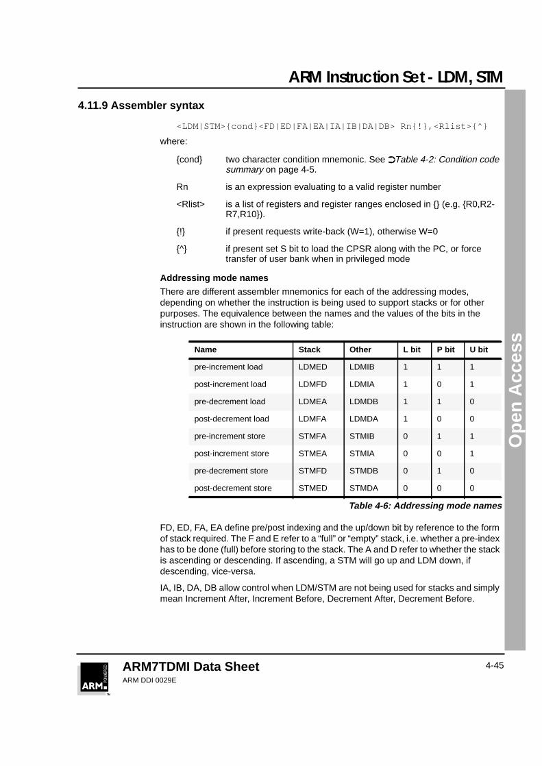
There are different assembler mnemonics for each of the addressing modes,depending on whether the instruction is being used to support stacks or for otherpurposes. The equivalence between the names and the values of the bits in theinstruction are shown in the following table:
FD, ED, FA, EA define pre/post indexing and the up/down bit by reference to the formof stack required. The F and E refer to a “full” or “empty” stack, i.e. whether a pre-indexhas to be done (full) before storing to the stack. The A and D refer to whether the stackis ascending or descending. If ascending, a STM will go up and LDM down, ifdescending, vice-versa.
IA, IB, DA, DB allow control when LDM/STM are not being used for stacks and simplymean Increment After, Increment Before, Decrement After, Decrement Before.
Name Stack Other L bit P bit U bit
pre-increment load LDMED LDMIB 1 1 1
post-increment load LDMFD LDMIA 1 0 1
pre-decrement load LDMEA LDMDB 1 1 0
post-decrement load LDMFA LDMDA 1 0 0
pre-increment store STMFA STMIB 0 1 1
post-increment store STMEA STMIA 0 0 1
pre-decrement store STMFD STMDB 0 1 0
post-decrement store STMED STMDA 0 0 0
Table 4-6: Addressing mode names
ARM Instruction Set - LDM, STM
ARM7TDMI Data SheetARM DDI 0029E
4-46
Ope
n A
cces
s
4.11.10Examples
LDMFD SP!,{R0,R1,R2} ; Unstack 3 registers.STMIA R0,{R0-R15} ; Save all registers.LDMFD SP!,{R15} ; R15 <- (SP),CPSR unchanged.LDMFD SP!,{R15}^ ; R15 <- (SP), CPSR <- SPSR_mode
; (allowed only in privileged modes).STMFD R13,{R0-R14}^ ; Save user mode regs on stack
; (allowed only in privileged modes).
These instructions may be used to save state on subroutine entry, and restore itefficiently on return to the calling routine:
STMED SP!,{R0-R3,R14} ; Save R0 to R3 to use as workspace; and R14 for returning.
BL somewhere ; This nested call will overwrite R14LDMED SP!,{R0-R3,R15} ; restore workspace and return.
ARM Instruction Set - SWP
ARM7TDMI Data SheetARM DDI 0029E
4-47
Ope
n A
cces
s
4.12 Single Data Swap (SWP)
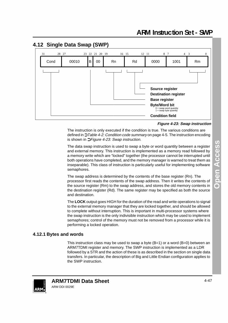
Figure 4-23: Swap instruction
The instruction is only executed if the condition is true. The various conditions aredefined in ➲Table 4-2: Condition code summary on page 4-5. The instruction encodingis shown in ➲Figure 4-23: Swap instruction.
The data swap instruction is used to swap a byte or word quantity between a registerand external memory. This instruction is implemented as a memory read followed bya memory write which are “locked” together (the processor cannot be interrupted untilboth operations have completed, and the memory manager is warned to treat them asinseparable). This class of instruction is particularly useful for implementing softwaresemaphores.
The swap address is determined by the contents of the base register (Rn). Theprocessor first reads the contents of the swap address. Then it writes the contents ofthe source register (Rm) to the swap address, and stores the old memory contents inthe destination register (Rd). The same register may be specified as both the sourceand destination.
The LOCK output goes HIGH for the duration of the read and write operations to signalto the external memory manager that they are locked together, and should be allowedto complete without interruption. This is important in multi-processor systems wherethe swap instruction is the only indivisible instruction which may be used to implementsemaphores; control of the memory must not be removed from a processor while it isperforming a locked operation.
4.12.1 Bytes and words
This instruction class may be used to swap a byte (B=1) or a word (B=0) between anARM7TDMI register and memory. The SWP instruction is implemented as a LDRfollowed by a STR and the action of these is as described in the section on single datatransfers. In particular, the description of Big and Little Endian configuration applies tothe SWP instruction.
0111215161920272831 23 78 4 3
Condition field
Cond Rn Rd 10010000 Rm00B00010
22 21
Destination registerSource register
Base registerByte/Word bit
0 = swap word quantity1 = swap byte quantity
ARM Instruction Set - SWP
ARM7TDMI Data SheetARM DDI 0029E
4-48
Ope
n A
cces
s
4.12.2 Use of R15
Do not use R15 as an operand (Rd, Rn or Rs) in a SWP instruction.
4.12.3 Data aborts
If the address used for the swap is unacceptable to a memory management system,the memory manager can flag the problem by driving ABORT HIGH. This can happenon either the read or the write cycle (or both), and in either case, the Data Abort trapwill be taken. It is up to the system software to resolve the cause of the problem, thenthe instruction can be restarted and the original program continued.
4.12.4 Instruction cycle times
Swap instructions take 1S + 2N +1I incremental cycles to execute, where S,N and Iare as defined in ➲6.2 Cycle Types on page 6-2.
4.12.5 Assembler syntax
<SWP>{cond}{B} Rd,Rm,[Rn]
{cond} two-character condition mnemonic. See ➲Table 4-2:Condition code summary on page 4-5.
{B} if B is present then byte transfer, otherwise word transfer
Rd,Rm,Rn are expressions evaluating to valid register numbers
4.12.6 Examples
SWP R0,R1,[R2] ; Load R0 with the word addressed by R2, and; store R1 at R2.
SWPB R2,R3,[R4] ; Load R2 with the byte addressed by R4, and; store bits 0 to 7 of R3 at R4.
SWPEQ R0,R0,[R1] ; Conditionally swap the contents of the; word addressed by R1 with R0.
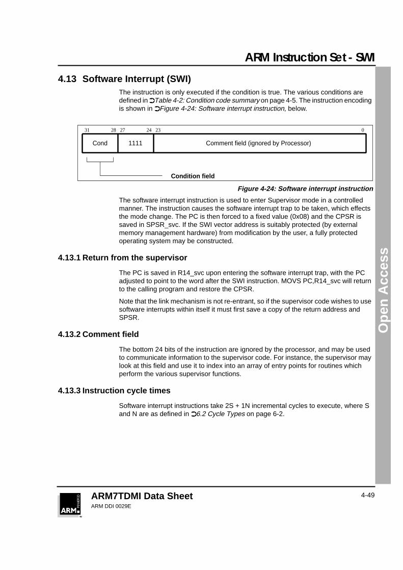
ARM Instruction Set - SWI
ARM7TDMI Data SheetARM DDI 0029E
4-49
Ope
n A
cces
s
4.13 Software Interrupt (SWI)The instruction is only executed if the condition is true. The various conditions aredefined in ➲Table 4-2: Condition code summary on page 4-5. The instruction encodingis shown in ➲Figure 4-24: Software interrupt instruction, below.
Figure 4-24: Software interrupt instruction
The software interrupt instruction is used to enter Supervisor mode in a controlledmanner. The instruction causes the software interrupt trap to be taken, which effectsthe mode change. The PC is then forced to a fixed value (0x08) and the CPSR issaved in SPSR_svc. If the SWI vector address is suitably protected (by externalmemory management hardware) from modification by the user, a fully protectedoperating system may be constructed.
4.13.1 Return from the supervisor
The PC is saved in R14_svc upon entering the software interrupt trap, with the PCadjusted to point to the word after the SWI instruction. MOVS PC,R14_svc will returnto the calling program and restore the CPSR.
Note that the link mechanism is not re-entrant, so if the supervisor code wishes to usesoftware interrupts within itself it must first save a copy of the return address andSPSR.
4.13.2 Comment field
The bottom 24 bits of the instruction are ignored by the processor, and may be usedto communicate information to the supervisor code. For instance, the supervisor maylook at this field and use it to index into an array of entry points for routines whichperform the various supervisor functions.
4.13.3 Instruction cycle times
Software interrupt instructions take 2S + 1N incremental cycles to execute, where Sand N are as defined in ➲6.2 Cycle Types on page 6-2.
31 28 27 24 23 0
Condition field
1111Cond Comment field (ignored by Processor)
ARM Instruction Set - SWI
ARM7TDMI Data SheetARM DDI 0029E
4-50
Ope
n A
cces
s
4.13.4 Assembler syntax
SWI{cond} <expression>
{cond} two character condition mnemonic, ➲Table 4-2: Conditioncode summary on page 4-5.
<expression> is evaluated and placed in the comment field (which isignored by ARM7TDMI).
4.13.5 Examples
SWI ReadC ; Get next character from read stream.SWI WriteI+”k” ; Output a “k” to the write stream.SWINE 0 ; Conditionally call supervisor
; with 0 in comment field.
Supervisor code
The previous examples assume that suitable supervisor code exists, for instance:
0x08 B Supervisor ; SWI entry pointEntryTable ; addresses of supervisor routines
DCD ZeroRtn DCD ReadCRtn DCD WriteIRtn . . .
Zero EQU 0ReadC EQU 256WriteI EQU 512
Supervisor
; SWI has routine required in bits 8-23 and data (if any) in; bits 0-7.; Assumes R13_svc points to a suitable stack
STMFD R13,{R0-R2,R14} ; Save work registers and return; address.
LDR R0,[R14,#-4] ; Get SWI instruction.BIC R0,R0,#0xFF000000 ; Clear top 8 bits.MOV R1,R0,LSR#8 ; Get routine offset.ADR R2,EntryTable ; Get start address of entry table.LDR R15,[R2,R1,LSL#2] ; Branch to appropriate routine.
WriteIRtn ; Enter with character in R0 bits 0-7.. . . . . .
LDMFD R13,{R0-R2,R15}^ ; Restore workspace and return,; restoring processor mode and flags.
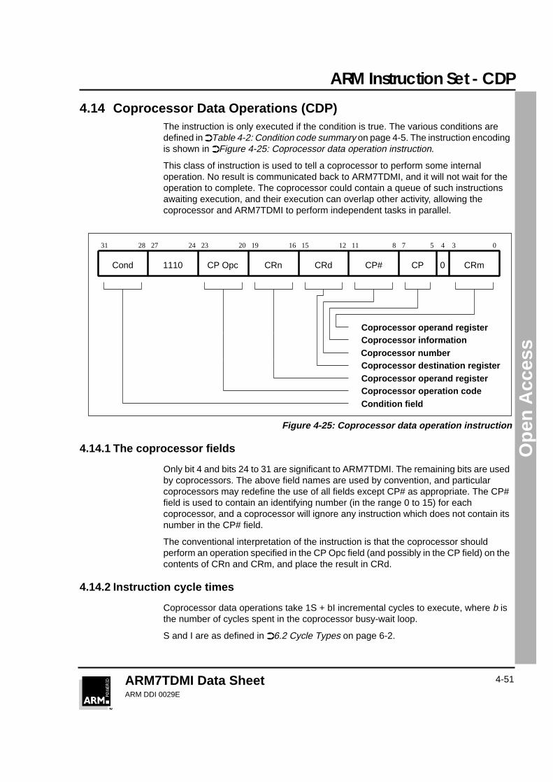
ARM Instruction Set - CDP
ARM7TDMI Data SheetARM DDI 0029E
4-51
Ope
n A
cces
s
4.14 Coprocessor Data Operations (CDP)The instruction is only executed if the condition is true. The various conditions aredefined in ➲Table 4-2: Condition code summary on page 4-5. The instruction encodingis shown in ➲Figure 4-25: Coprocessor data operation instruction.
This class of instruction is used to tell a coprocessor to perform some internaloperation. No result is communicated back to ARM7TDMI, and it will not wait for theoperation to complete. The coprocessor could contain a queue of such instructionsawaiting execution, and their execution can overlap other activity, allowing thecoprocessor and ARM7TDMI to perform independent tasks in parallel.
Figure 4-25: Coprocessor data operation instruction
4.14.1 The coprocessor fields
Only bit 4 and bits 24 to 31 are significant to ARM7TDMI. The remaining bits are usedby coprocessors. The above field names are used by convention, and particularcoprocessors may redefine the use of all fields except CP# as appropriate. The CP#field is used to contain an identifying number (in the range 0 to 15) for eachcoprocessor, and a coprocessor will ignore any instruction which does not contain itsnumber in the CP# field.
The conventional interpretation of the instruction is that the coprocessor shouldperform an operation specified in the CP Opc field (and possibly in the CP field) on thecontents of CRn and CRm, and place the result in CRd.
4.14.2 Instruction cycle times
Coprocessor data operations take 1S + bI incremental cycles to execute, where b isthe number of cycles spent in the coprocessor busy-wait loop.
S and I are as defined in ➲6.2 Cycle Types on page 6-2.
Cond
011121516192024272831 23
CRd CP#
78
1110 CP Opc CRn CP 0 CRm
5 4 3
Coprocessor number
Condition field
Coprocessor information Coprocessor operand register
Coprocessor destination register Coprocessor operand register Coprocessor operation code
ARM Instruction Set - CDP
ARM7TDMI Data SheetARM DDI 0029E
4-52
Ope
n A
cces
s
4.14.3 Assembler syntax
CDP{cond} p#,<expression1>,cd,cn,cm{,<expression2>}
{cond} two character condition mnemonic. See ➲Table 4-2:Condition code summary on page 4-5.
p# the unique number of the required coprocessor
<expression1> evaluated to a constant and placed in the CP Opc field
cd, cn and cm evaluate to the valid coprocessor register numbers CRd, CRnand CRm respectively
<expression2> where present is evaluated to a constant and placed in theCP field
4.14.4 Examples
CDP p1,10,c1,c2,c3 ; Request coproc 1 to do operation 10; on CR2 and CR3, and put the result; in CR1.
CDPEQ p2,5,c1,c2,c3,2 ; If Z flag is set request coproc 2; to do operation 5 (type 2) on CR2; and CR3,and put the result in CR1.
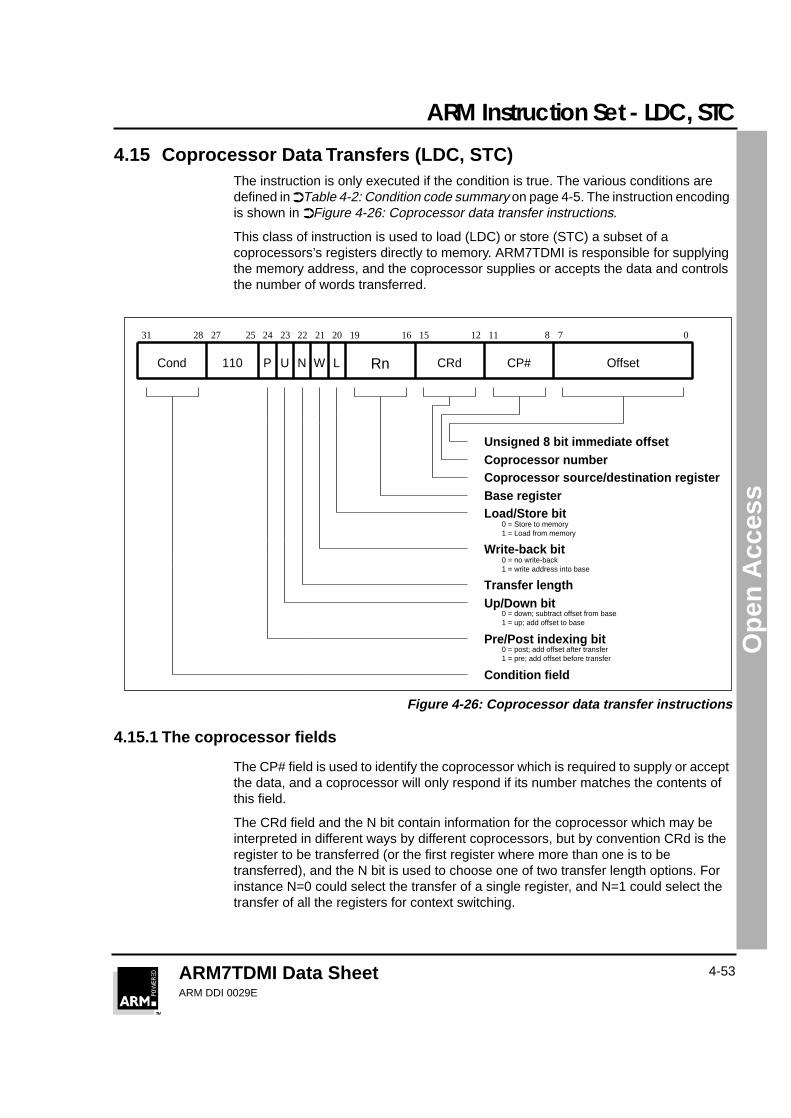
ARM Instruction Set - LDC, STC
ARM7TDMI Data SheetARM DDI 0029E
4-53
Ope
n A
cces
s
4.15 Coprocessor Data Transfers (LDC, STC)The instruction is only executed if the condition is true. The various conditions aredefined in ➲Table 4-2: Condition code summary on page 4-5. The instruction encodingis shown in ➲Figure 4-26: Coprocessor data transfer instructions.
This class of instruction is used to load (LDC) or store (STC) a subset of acoprocessors’s registers directly to memory. ARM7TDMI is responsible for supplyingthe memory address, and the coprocessor supplies or accepts the data and controlsthe number of words transferred.
Figure 4-26: Coprocessor data transfer instructions
4.15.1 The coprocessor fields
The CP# field is used to identify the coprocessor which is required to supply or acceptthe data, and a coprocessor will only respond if its number matches the contents ofthis field.
The CRd field and the N bit contain information for the coprocessor which may beinterpreted in different ways by different coprocessors, but by convention CRd is theregister to be transferred (or the first register where more than one is to betransferred), and the N bit is used to choose one of two transfer length options. Forinstance N=0 could select the transfer of a single register, and N=1 could select thetransfer of all the registers for context switching.
Cond Rn
0111215161920212425272831
P U W L
2223
110 N CRd CP# Offset
78
Coprocessor number Unsigned 8 bit immediate offset
Base registerLoad/Store bit
0 = Store to memory1 = Load from memory
Write-back bit0 = no write-back1 = write address into base
Coprocessor source/destination register
Pre/Post indexing bit
Up/Down bit0 = down; subtract offset from base1 = up; add offset to base
0 = post; add offset after transfer
Transfer length
Condition field1 = pre; add offset before transfer
ARM Instruction Set - LDC, STC
ARM7TDMI Data SheetARM DDI 0029E
4-54
Ope
n A
cces
s
4.15.2 Addressing modes
ARM7TDMI is responsible for providing the address used by the memory system forthe transfer, and the addressing modes available are a subset of those used in singledata transfer instructions. Note, however, that the immediate offsets are 8 bits wideand specify word offsets for coprocessor data transfers, whereas they are 12 bits wideand specify byte offsets for single data transfers.
The 8 bit unsigned immediate offset is shifted left 2 bits and either added to (U=1) orsubtracted from (U=0) the base register (Rn); this calculation may be performed eitherbefore (P=1) or after (P=0) the base is used as the transfer address. The modifiedbase value may be overwritten back into the base register (if W=1), or the old value ofthe base may be preserved (W=0). Note that post-indexed addressing modes requireexplicit setting of the W bit, unlike LDR and STR which always write-back when post-indexed.
The value of the base register, modified by the offset in a pre-indexed instruction, isused as the address for the transfer of the first word. The second word (if more thanone is transferred) will go to or come from an address one word (4 bytes) higher thanthe first transfer, and the address will be incremented by one word for eachsubsequent transfer.
4.15.3 Address alignment
The base address should normally be a word aligned quantity. The bottom 2 bits of theaddress will appear on A[1:0] and might be interpreted by the memory system.
4.15.4 Use of R15
If Rn is R15, the value used will be the address of the instruction plus 8 bytes. Basewrite-back to R15 must not be specified.
4.15.5 Data aborts
If the address is legal but the memory manager generates an abort, the data trap willbe taken. The write-back of the modified base will take place, but all other processorstate will be preserved. The coprocessor is partly responsible for ensuring that thedata transfer can be restarted after the cause of the abort has been resolved, and mustensure that any subsequent actions it undertakes can be repeated when theinstruction is retried.
4.15.6 Instruction cycle times
Coprocessor data transfer instructions take (n-1)S + 2N + bI incremental cycles toexecute, where:
n is the number of words transferred.
b is the number of cycles spent in the coprocessor busy-wait loop.
S, N and I are as defined in ➲6.2 Cycle Types on page 6-2.
ARM Instruction Set - LDC, STC
ARM7TDMI Data SheetARM DDI 0029E
4-55
Ope
n A
cces
s
4.15.7 Assembler syntax
<LDC|STC>{cond}{L} p#,cd,<Address>
LDC load from memory to coprocessor
STC store from coprocessor to memory
{L} when present perform long transfer (N=1), otherwise perform shorttransfer (N=0)
{cond} two character condition mnemonic. See ➲Table 4-2: Condition codesummary on page 4-5.
p# the unique number of the required coprocessor
cd is an expression evaluating to a valid coprocessor register numberthat is placed in the CRd field
<Address> can be:
1 An expression which generates an address:
<expression>
The assembler will attempt to generate an instruction usingthe PC as a base and a corrected immediate offset to addressthe location given by evaluating the expression. This will be aPC relative, pre-indexed address. If the address is out ofrange, an error will be generated.
2 A pre-indexed addressing specification:
[Rn] offset of zero
[Rn,<#expression>]{!} offset of <expression> bytes
3 A post-indexed addressing specification:
[Rn],<#expression> offset of <expression> bytes
{!} write back the base register(set the W bit) if! is present
Rn is an expression evaluatingto a valid ARM7TDMIregister number.
Note If Rn is R15, the assembler will subtract 8 from the offset value to allow for ARM7TDMIpipelining.
ARM Instruction Set - LDC, STC
ARM7TDMI Data SheetARM DDI 0029E
4-56
Ope
n A
cces
s
4.15.8 Examples
LDC p1,c2,table ; Load c2 of coproc 1 from address; table, using a PC relative address.
STCEQL p2,c3,[R5,#24]!; Conditionally store c3 of coproc 2; into an address 24 bytes up from R5,; write this address back to R5, and use; long transfer option (probably to; store multiple words).
Note Although the address offset is expressed in bytes, the instruction offset field is inwords. The assembler will adjust the offset appropriately.
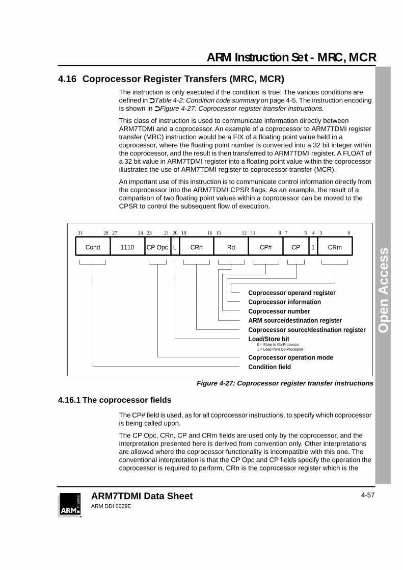
ARM Instruction Set - MRC, MCR
ARM7TDMI Data SheetARM DDI 0029E
4-57
Ope
n A
cces
s
4.16 Coprocessor Register Transfers (MRC, MCR)The instruction is only executed if the condition is true. The various conditions aredefined in ➲Table 4-2: Condition code summary on page 4-5. The instruction encodingis shown in ➲Figure 4-27: Coprocessor register transfer instructions.
This class of instruction is used to communicate information directly betweenARM7TDMI and a coprocessor. An example of a coprocessor to ARM7TDMI registertransfer (MRC) instruction would be a FIX of a floating point value held in acoprocessor, where the floating point number is converted into a 32 bit integer withinthe coprocessor, and the result is then transferred to ARM7TDMI register. A FLOAT ofa 32 bit value in ARM7TDMI register into a floating point value within the coprocessorillustrates the use of ARM7TDMI register to coprocessor transfer (MCR).
An important use of this instruction is to communicate control information directly fromthe coprocessor into the ARM7TDMI CPSR flags. As an example, the result of acomparison of two floating point values within a coprocessor can be moved to theCPSR to control the subsequent flow of execution.
Figure 4-27: Coprocessor register transfer instructions
4.16.1 The coprocessor fields
The CP# field is used, as for all coprocessor instructions, to specify which coprocessoris being called upon.
The CP Opc, CRn, CP and CRm fields are used only by the coprocessor, and theinterpretation presented here is derived from convention only. Other interpretationsare allowed where the coprocessor functionality is incompatible with this one. Theconventional interpretation is that the CP Opc and CP fields specify the operation thecoprocessor is required to perform, CRn is the coprocessor register which is the
21
Cond
011121516192024272831 23
CP#
78
1110 CRn CP CRm
5 4 3
1LCP Opc Rd
Coprocessor number Coprocessor information Coprocessor operand register
Coprocessor operation mode Condition field
Load/Store bit0 = Store to Co-Processor1 = Load from Co-Processor
ARM source/destination registerCoprocessor source/destination register
ARM Instruction Set - MRC, MCR
ARM7TDMI Data SheetARM DDI 0029E
4-58
Ope
n A
cces
s
source or destination of the transferred information, and CRm is a second coprocessorregister which may be involved in some way which depends on the particular operationspecified.
4.16.2 Transfers to R15
When a coprocessor register transfer to ARM7TDMI has R15 as the destination, bits31, 30, 29 and 28 of the transferred word are copied into the N, Z, C and V flagsrespectively. The other bits of the transferred word are ignored, and the PC and otherCPSR bits are unaffected by the transfer.
4.16.3 Transfers from R15
A coprocessor register transfer from ARM7TDMI with R15 as the source register willstore the PC+12.
4.16.4 Instruction cycle times
MRC instructions take 1S + (b+1)I +1C incremental cycles to execute, where S, I andC are as defined in ➲6.2 Cycle Types on page 6-2.
MCR instructions take 1S + bI +1C incremental cycles to execute, where b is thenumber of cycles spent in the coprocessor busy-wait loop.
4.16.5 Assembler syntax
<MCR|MRC>{cond} p#,<expression1>,Rd,cn,cm{,<expression2>}
MRC move from coprocessor to ARM7TDMI register (L=1)
MCR move from ARM7TDMI register to coprocessor (L=0)
{cond} two character condition mnemonic. See ➲Table 4-2:Condition code summary on page 4-5.
p# the unique number of the required coprocessor
<expression1> evaluated to a constant and placed in the CP Opc field
Rd is an expression evaluating to a valid ARM7TDMI registernumber
cn and cm are expressions evaluating to the valid coprocessor registernumbers CRn and CRm respectively
<expression2> where present is evaluated to a constant and placed in theCP field
ARM Instruction Set - MRC, MCR
ARM7TDMI Data SheetARM DDI 0029E
4-59
Ope
n A
cces
s
4.16.6 Examples
MRC p2,5,R3,c5,c6 ; Request coproc 2 to perform operation 5; on c5 and c6, and transfer the (single; 32 bit word) result back to R3.
MCR p6,0,R4,c5,c6 ; Request coproc 6 to perform operation 0; on R4 and place the result in c6.
MRCEQ p3,9,R3,c5,c6,2 ; Conditionally request coproc 3 to; perform operation 9 (type 2) on c5 and; c6, and transfer the result back to R3.
ARM Instruction Set - Undefined
ARM7TDMI Data SheetARM DDI 0029E
4-60
Ope
n A
cces
s
4.17 Undefined InstructionThe instruction is only executed if the condition is true. The various conditions aredefined in ➲Table 4-2: Condition code summary on page 4-5. The instruction formatis shown in ➲Figure 4-28: Undefined instruction.
Figure 4-28: Undefined instruction
If the condition is true, the undefined instruction trap will be taken.
Note that the undefined instruction mechanism involves offering this instruction to anycoprocessors which may be present, and all coprocessors must refuse to accept it bydriving CPA and CPB HIGH.
4.17.1 Instruction cycle times
This instruction takes 2S + 1I + 1N cycles, where S, N and I are as defined in ➲6.2Cycle Types on page 6-2.
4.17.2 Assembler syntax
The assembler has no mnemonics for generating this instruction. If it is adopted in thefuture for some specified use, suitable mnemonics will be added to the assembler.Until such time, this instruction must not be used.
Cond
024272831 5 4 3
1011 xxxx
25
xxxxxxxxxxxxxxxxxxxx
ARM Instruction Set - Examples
ARM7TDMI Data SheetARM DDI 0029E
4-61
Ope
n A
cces
s
4.18 Instruction Set ExamplesThe following examples show ways in which the basic ARM7TDMI instructions cancombine to give efficient code. None of these methods saves a great deal of executiontime (although they may save some), mostly they just save code.
4.18.1 Using the conditional instructions
Using conditionals for logical ORCMP Rn,#p ; If Rn=p OR Rm=q THEN GOTO Label.BEQ LabelCMP Rm,#qBEQ Label
This can be replaced by
CMP Rn,#pCMPNE Rm,#q ; If condition not satisfied try
; other test.BEQ Label
Absolute valueTEQ Rn,#0 ; Test signRSBMI Rn,Rn,#0 ; and 2's complement if necessary.
Multiplication by 4, 5 or 6 (run time)MOV Rc,Ra,LSL#2 ; Multiply by 4,CMP Rb,#5 ; test value,ADDCS Rc,Rc,Ra ; complete multiply by 5,ADDHI Rc,Rc,Ra ; complete multiply by 6.
Combining discrete and range testsTEQ Rc,#127 ; Discrete test,CMPNE Rc,#” ”-1 ; range testMOVLS Rc,#”.” ; IF Rc<=” ” OR Rc=ASCII(127)
; THEN Rc:=”.”
Division and remainder
A number of divide routines for specific applications are provided in source form aspart of the ANSI C library provided with the ARM Cross Development Toolkit, availablefrom your supplier. A short general purpose divide routine follows.
; Enter with numbers in Ra and Rb.;
MOV Rcnt,#1 ; Bit to control the division.Div1 CMP Rb,#0x80000000 ; Move Rb until greater than Ra.
CMPCC Rb,RaMOVCC Rb,Rb,ASL#1MOVCC Rcnt,Rcnt,ASL#1BCC Div1MOV Rc,#0
ARM Instruction Set - Examples
ARM7TDMI Data SheetARM DDI 0029E
4-62
Ope
n A
cces
s
Div2 CMP Ra,Rb ; Test for possible subtraction.SUBCS Ra,Ra,Rb ; Subtract if ok,ADDCS Rc,Rc,Rcnt ; put relevant bit into resultMOVS Rcnt,Rcnt,LSR#1 ; shift control bitMOVNE Rb,Rb,LSR#1 ; halve unless finished.BNE Div2
;; Divide result in Rc,; remainder in Ra.
Overflow detection in the ARM7TDMI
1 Overflow in unsigned multiply with a 32 bit result
UMULL Rd,Rt,Rm,Rn ;3 to 6 cyclesTEQ Rt,#0 ;+1 cycle and a registerBNE overflow
2 Overflow in signed multiply with a 32 bit result
SMULL Rd,Rt,Rm,Rn ;3 to 6 cyclesTEQ Rt,Rd ASR#31 ;+1 cycle and a registerBNE overflow
3 Overflow in unsigned multiply accumulate with a 32 bit result
UMLAL Rd,Rt,Rm,Rn ;4 to 7 cyclesTEQ Rt,#0 ;+1 cycle and a registerBNE overflow
4 Overflow in signed multiply accumulate with a 32 bit result
SMLAL Rd,Rt,Rm,Rn ;4 to 7 cyclesTEQ Rt,Rd, ASR#31 ;+1 cycle and a registerBNE overflow
5 Overflow in unsigned multiply accumulate with a 64 bit result
UMULL Rl,Rh,Rm,Rn ;3 to 6 cyclesADDS Rl,Rl,Ra1 ;lower accumulateADC Rh,Rh,Ra2 ;upper accumulateBCS overflow ;1 cycle and 2 registers
6 Overflow in signed multiply accumulate with a 64 bit result
SMULL Rl,Rh,Rm,Rn ;3 to 6 cyclesADDS Rl,Rl,Ra1 ;lower accumulateADC Rh,Rh,Ra2 ;upper accumulateBVS overflow ;1 cycle and 2 registers
Note Overflow checking is not applicable to unsigned and signed multiplies with a 64-bitresult, since overflow does not occur in such calculations.
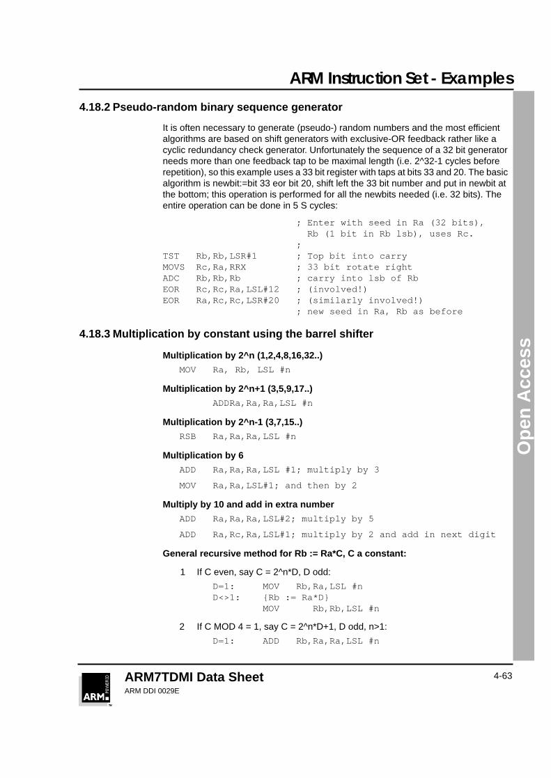
ARM Instruction Set - Examples
ARM7TDMI Data SheetARM DDI 0029E
4-63
Ope
n A
cces
s
4.18.2 Pseudo-random binary sequence generator
It is often necessary to generate (pseudo-) random numbers and the most efficientalgorithms are based on shift generators with exclusive-OR feedback rather like acyclic redundancy check generator. Unfortunately the sequence of a 32 bit generatorneeds more than one feedback tap to be maximal length (i.e. 2^32-1 cycles beforerepetition), so this example uses a 33 bit register with taps at bits 33 and 20. The basicalgorithm is newbit:=bit 33 eor bit 20, shift left the 33 bit number and put in newbit atthe bottom; this operation is performed for all the newbits needed (i.e. 32 bits). Theentire operation can be done in 5 S cycles:
; Enter with seed in Ra (32 bits), Rb (1 bit in Rb lsb), uses Rc.;
TST Rb,Rb,LSR#1 ; Top bit into carryMOVS Rc,Ra,RRX ; 33 bit rotate rightADC Rb,Rb,Rb ; carry into lsb of RbEOR Rc,Rc,Ra,LSL#12 ; (involved!)EOR Ra,Rc,Rc,LSR#20 ; (similarly involved!)
; new seed in Ra, Rb as before
4.18.3 Multiplication by constant using the barrel shifter
Multiplication by 2^n (1,2,4,8,16,32..)
MOV Ra, Rb, LSL #n
Multiplication by 2^n+1 (3,5,9,17..)
ADDRa,Ra,Ra,LSL #n
Multiplication by 2^n-1 (3,7,15..)
RSB Ra,Ra,Ra,LSL #n
Multiplication by 6
ADD Ra,Ra,Ra,LSL #1; multiply by 3
MOV Ra,Ra,LSL#1; and then by 2
Multiply by 10 and add in extra number
ADD Ra,Ra,Ra,LSL#2; multiply by 5
ADD Ra,Rc,Ra,LSL#1; multiply by 2 and add in next digit
General recursive method for Rb := Ra*C, C a constant:
1 If C even, say C = 2^n*D, D odd:
D=1: MOV Rb,Ra,LSL #nD<>1: {Rb := Ra*D}
MOV Rb,Rb,LSL #n
2 If C MOD 4 = 1, say C = 2^n*D+1, D odd, n>1:
D=1: ADD Rb,Ra,Ra,LSL #n
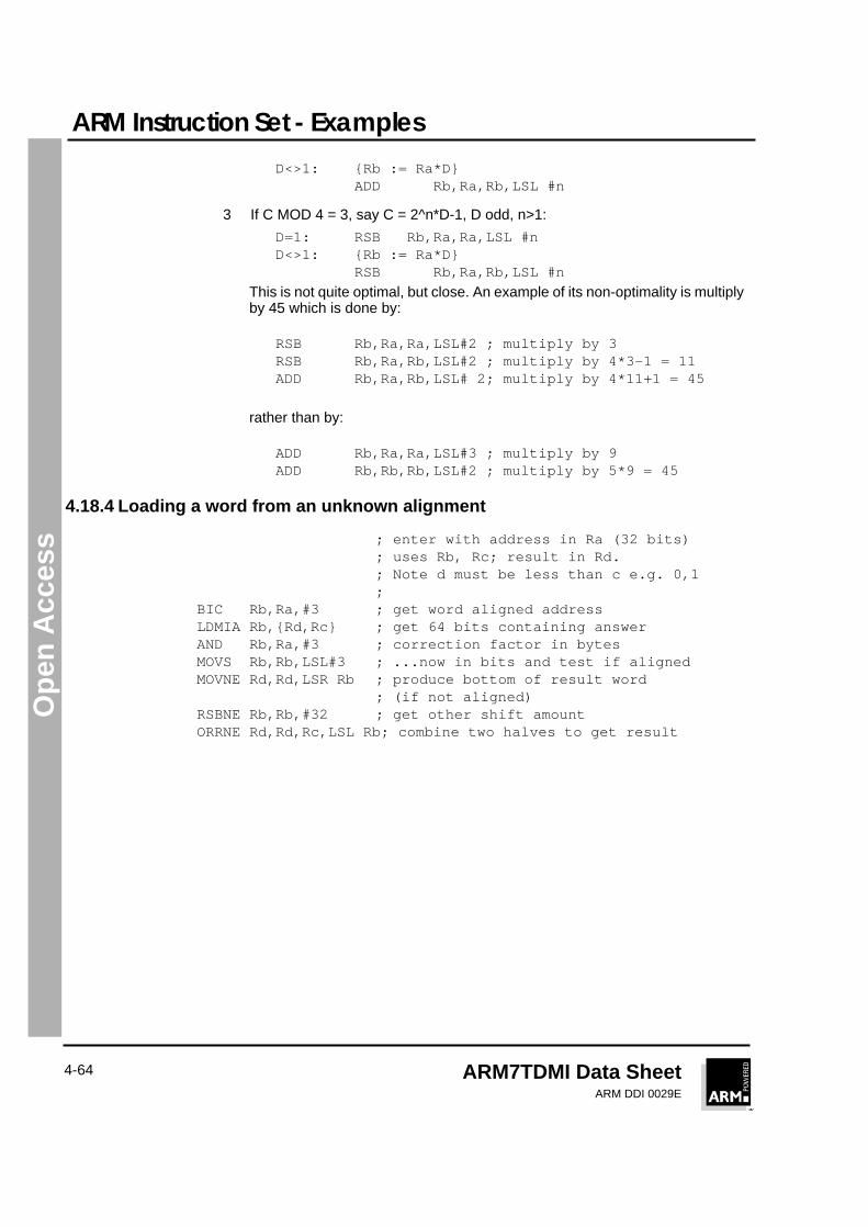
ARM Instruction Set - Examples
ARM7TDMI Data SheetARM DDI 0029E
4-64
Ope
n A
cces
s
D<>1: {Rb := Ra*D}ADD Rb,Ra,Rb,LSL #n
3 If C MOD 4 = 3, say C = 2^n*D-1, D odd, n>1:
D=1: RSB Rb,Ra,Ra,LSL #nD<>1: {Rb := Ra*D}
RSB Rb,Ra,Rb,LSL #n
This is not quite optimal, but close. An example of its non-optimality is multiplyby 45 which is done by:
RSB Rb,Ra,Ra,LSL#2 ; multiply by 3RSB Rb,Ra,Rb,LSL#2 ; multiply by 4*3-1 = 11ADD Rb,Ra,Rb,LSL# 2; multiply by 4*11+1 = 45
rather than by:
ADD Rb,Ra,Ra,LSL#3 ; multiply by 9ADD Rb,Rb,Rb,LSL#2 ; multiply by 5*9 = 45
4.18.4 Loading a word from an unknown alignment
; enter with address in Ra (32 bits); uses Rb, Rc; result in Rd.; Note d must be less than c e.g. 0,1;
BIC Rb,Ra,#3 ; get word aligned addressLDMIA Rb,{Rd,Rc} ; get 64 bits containing answerAND Rb,Ra,#3 ; correction factor in bytesMOVS Rb,Rb,LSL#3 ; ...now in bits and test if alignedMOVNE Rd,Rd,LSR Rb ; produce bottom of result word
; (if not aligned)RSBNE Rb,Rb,#32 ; get other shift amountORRNE Rd,Rd,Rc,LSL Rb; combine two halves to get result
![[XLS] · Web viewSTR 20015 STR 30105 STR 30115 STR 30123 STR 30125 STR 30130 STR 40090 ORİ STR 40115 STR 41090 ORİ STR 44115 STR 45111 STR 50020 STR 50103A STR 50112 STR 50113A](https://img.pdfslide.us/doc/110x75/5ad04b0c7f8b9a1d328e1e93/xls-viewstr-20015-str-30105-str-30115-str-30123-str-30125-str-30130-str-40090.jpg)
![Architecture des ordinateurs V - Supélecwdi.supelec.fr/architecture/downloads/Slides/Archi-05... · 2019-07-04 · Récapitulons Instructions ldr rx, adresse rx Mem[adresse] str](https://img.pdfslide.us/doc/110x75/5f3fad1567dbb65bd73a86c0/architecture-des-ordinateurs-v-sup-2019-07-04-rcapitulons-instructions-ldr.jpg)