Embed Size (px)
Citation preview

ARM® CoreSight™ SoC-400Revision: r3p1
Technical Reference Manual
Copyright © 2011-2013 ARM. All rights reserved.ARM DDI 0480F (ID100313)

ARM CoreSight SoC-400Technical Reference Manual
Copyright © 2011-2013 ARM. All rights reserved.
Release Information
The following changes have been made to this book.
Proprietary Notice
Words and logos marked with ® or ™ are registered trademarks or trademarks of ARM in the EU and other countries, except as otherwise stated below in this proprietary notice. Other brands and names mentioned herein may be the trademarks of their respective owners.
Neither the whole nor any part of the information contained in, or the product described in, this document may be adapted or reproduced in any material form except with the prior written permission of the copyright holder.
The product described in this document is subject to continuous developments and improvements. All particulars of the product and its use contained in this document are given by ARM in good faith. However, all warranties implied or expressed, including but not limited to implied warranties of merchantability, or fitness for purpose, are excluded.
This document is intended only to assist the reader in the use of the product. ARM shall not be liable for any loss or damage arising from the use of any information in this document, or any error or omission in such information, or any incorrect use of the product.
Where the term ARM is used it means “ARM or any of its subsidiaries as appropriate”.
Confidentiality Status
This document is Non-Confidential. The right to use, copy and disclose this document may be subject to license restrictions in accordance with the terms of the agreement entered into by ARM and the party that ARM delivered this document to.
Product Status
The information in this document is final, that is for a developed product.
Web Address
http://www.arm.com
Change history
Date Issue Confidentiality Change
04 November 2011 A Non-Confidential First release for r0p0
16 April 2012 B Non-Confidential First release for r1p0
27 September 2012 C Non-Confidential First release for r2p0
14 December 2012 D Non-Confidential First release for r2p1
28 June 2013 E Non-Confidential First release for r3p0
26 September 2013 F Non-Confidential First release for r3p1
ARM DDI 0480F Copyright © 2011-2013 ARM. All rights reserved. iiID100313 Non-Confidential

ContentsARM CoreSight SoC-400 Technical Reference Manual
PrefaceAbout this book ............................................................................................. viiFeedback ....................................................................................................... xi
Chapter 1 Introduction1.1 About CoreSight SoC-400 .......................................................................... 1-21.2 Compliance ................................................................................................. 1-61.3 Features ...................................................................................................... 1-71.4 Interfaces .................................................................................................... 1-81.5 Configurable options ................................................................................... 1-91.6 Test features ............................................................................................. 1-101.7 Product documentation and design flow ................................................... 1-111.8 Product revisions ...................................................................................... 1-13
Chapter 2 Functional Overview2.1 DAP components ........................................................................................ 2-22.2 APB components ........................................................................................ 2-92.3 ATB interconnect components .................................................................. 2-122.4 Timestamp components ........................................................................... 2-192.5 Embedded Cross Trigger components ..................................................... 2-242.6 Trace sink components ............................................................................. 2-262.7 Authentication bridges .............................................................................. 2-282.8 Granular Power Requestor ....................................................................... 2-30
Chapter 3 Programmers Model3.1 About the programmers model ................................................................... 3-2
ARM DDI 0480F Copyright © 2011-2013 ARM. All rights reserved. iiiID100313 Non-Confidential

3.2 Granular Power Requestor register summary ............................................ 3-33.3 Granular Power Requestor register descriptions ........................................ 3-43.4 APB interconnect register summary ......................................................... 3-223.5 APB interconnect register descriptions ..................................................... 3-233.6 ATB funnel register summary ................................................................... 3-303.7 ATB funnel register descriptions ............................................................... 3-313.8 ATB replicator register summary .............................................................. 3-523.9 ATB replicator register descriptions .......................................................... 3-533.10 ETB register summary .............................................................................. 3-693.11 ETB register descriptions .......................................................................... 3-713.12 TPIU register summary ............................................................................. 3-973.13 TPIU register descriptions ........................................................................ 3-993.14 CTI register summary ............................................................................. 3-1353.15 CTI register descriptions ......................................................................... 3-1373.16 DAP register summary ............................................................................ 3-1713.17 DAP register descriptions ....................................................................... 3-1753.18 Timestamp generator register summary ................................................. 3-2033.19 Timestamp generator registers description ............................................ 3-205
Chapter 4 Debug Access Port4.1 About the Debug Access Port ..................................................................... 4-24.2 SWJ-DP ...................................................................................................... 4-54.3 DAPBUS interconnect ............................................................................. 4-154.4 DAPBUS asynchronous bridge ................................................................. 4-164.5 DAPBUS synchronous bridge ................................................................... 4-174.6 JTAG-AP ................................................................................................... 4-184.7 AXI-AP ...................................................................................................... 4-204.8 AHB-AP .................................................................................................... 4-264.9 APB-AP ..................................................................................................... 4-30
Chapter 5 APB Interconnect Components5.1 APB Interconnect with ROM table .............................................................. 5-25.2 APB asynchronous bridge .......................................................................... 5-55.3 APB synchronous bridge ............................................................................ 5-6
Chapter 6 ATB Interconnect Components6.1 ATB replicator ............................................................................................. 6-26.2 ATB funnel .................................................................................................. 6-36.3 ATB upsizer ................................................................................................ 6-66.4 ATB downsizer ............................................................................................ 6-76.5 ATB asynchronous bridge .......................................................................... 6-86.6 ATB synchronous bridge .......................................................................... 6-10
Chapter 7 Timestamp Components7.1 About the timestamp components .............................................................. 7-27.2 Timestamp generator .................................................................................. 7-37.3 Timestamp encoder .................................................................................... 7-57.4 Narrow timestamp replicator ....................................................................... 7-67.5 Narrow timestamp asynchronous bridge .................................................... 7-77.6 Narrow timestamp synchronous bridge ...................................................... 7-97.7 Timestamp decoder .................................................................................. 7-107.8 Timestamp interpolator ............................................................................. 7-11
Chapter 8 Embedded Cross Trigger8.1 Cross-triggering components ...................................................................... 8-28.2 CTI .............................................................................................................. 8-38.3 CTM ............................................................................................................ 8-58.4 Event asynchronous bridge ........................................................................ 8-68.5 Register slice .............................................................................................. 8-7
ARM DDI 0480F Copyright © 2011-2013 ARM. All rights reserved. ivID100313 Non-Confidential

Chapter 9 Trace Port Interface Unit9.1 About the Trace Port Interface Unit ............................................................ 9-29.2 Clocks and resets ....................................................................................... 9-39.3 Functional interfaces ................................................................................... 9-49.4 Trace out port ............................................................................................. 9-59.5 Trace port triggers ..................................................................................... 9-79.6 Programming the TPIU for trace capture .................................................... 9-89.7 Example configuration scenarios ................................................................ 9-99.8 TPIU pattern generator ............................................................................. 9-12
Chapter 10 Embedded Trace Buffer10.1 About the ETB .......................................................................................... 10-210.2 Clocks and resets ..................................................................................... 10-310.3 Functional Interfaces ................................................................................ 10-410.4 ETB trace capture and formatting ............................................................. 10-510.5 ETB RAM support ................................................................................... 10-11
Appendix A Signal DescriptionsA.1 Debug Access Port signals ......................................................................... A-2A.2 APB component signals ............................................................................ A-14A.3 ATB interconnect signals .......................................................................... A-18A.4 Timestamp component signals ................................................................. A-25A.5 Trigger component signals ....................................................................... A-32A.6 Trace sink signals ..................................................................................... A-35A.7 Authentication and event bridges ............................................................. A-38A.8 Granular power requestor signals ............................................................. A-40
Appendix B Revisions
ARM DDI 0480F Copyright © 2011-2013 ARM. All rights reserved. vID100313 Non-Confidential

Preface
This preface introduces the ARM® CoreSight™ SoC-400 Technical Reference Manual. It contains the following sections:• About this book on page vii.• Feedback on page xi.
ARM DDI 0480F Copyright © 2011-2013 ARM. All rights reserved. viID100313 Non-Confidential

Preface
About this bookThis book is for Technical Reference Manual (TRM) for the CoreSight SoC-400 components.
Product revision status
The rnpn identifier indicates the revision status of the product described in this book, where:rn Identifies the major revision of the product.pn Identifies the minor revision or modification status of the product.
Intended audience
This book is written for the following audiences:
• Hardware and software engineers who want to incorporate CoreSight SoC-400 into their design and produce real-time instruction and data trace information from a SoC.
• Software engineers writing tools to use CoreSight SoC-400.
This book assumes that readers are familiar with AMBA bus design and JTAG methodology.
Using this book
This book is organized into the following chapters:
Chapter 1 Introduction Read this for an overview of the CoreSight SoC-400 components.
Chapter 2 Functional Overview Read this for a description of the major functional blocks and the operation of CoreSight SoC-400.
Chapter 3 Programmers Model Read this for a description of the memory map and registers.
Chapter 4 Debug Access Port Read this for a description of the Debug Access Port (DAP) components.
Chapter 5 APB Interconnect Components Read this for a description of the APB interconnect components.
Chapter 6 ATB Interconnect Components Read this for a description of the ATB interconnect components.
Chapter 7 Timestamp Components Read this for a description of the timestamp components.
Chapter 8 Embedded Cross Trigger Read this for a description of the Embedded Cross Trigger (ECT) components.
Chapter 9 Trace Port Interface Unit Read this for a description of the Trace Port Interface Unit (TPIU) components.
Chapter 10 Embedded Trace Buffer Read this for a description of the Embedded Trace Buffer (ETB) components.
ARM DDI 0480F Copyright © 2011-2013 ARM. All rights reserved. viiID100313 Non-Confidential

Preface
Appendix A Signal Descriptions Read this for a description of the CoreSight SoC-400 signals.
Appendix B Revisions Read this for a description of the technical changes between released issues of this book.
Glossary
The ARM® Glossary is a list of terms used in ARM documentation, together with definitions for those terms. The ARM® Glossary does not contain terms that are industry standard unless the ARM meaning differs from the generally accepted meaning.
See ARM® Glossary, http://infocenter.arm.com/help/topic/com.arm.doc.aeg0014-/index.html.
Conventions
This book uses the conventions that are described in:• Typographical conventions.• Timing diagrams.• Signals on page ix.
Typographical conventions
The following table describes the typographical conventions:
Timing diagrams
The figure Key to timing diagram conventions on page ix explains the components used in timing diagrams. Variations, when they occur, have clear labels. You must not assume any timing information that is not explicit in the diagrams.
Typographical conventions
Style Purpose
italic Introduces special terminology, denotes cross-references, and citations.
bold Highlights interface elements, such as menu names. Denotes signal names. Also used for terms in descriptive lists, where appropriate.
monospace Denotes text that you can enter at the keyboard, such as commands, file and program names, and source code.
monospace Denotes a permitted abbreviation for a command or option. You can enter the underlined text instead of the full command or option name.
monospace italic Denotes arguments to monospace text where the argument is to be replaced by a specific value.
monospace bold Denotes language keywords when used outside example code.
<and> Encloses replaceable terms for assembler syntax where they appear in code or code fragments. For example:MRC p15, 0 <Rd>, <CRn>, <CRm>, <Opcode_2>
SMALL CAPITALS Used in body text for a few terms that have specific technical meanings, that are defined in the ARM® glossary. For example, IMPLEMENTATION DEFINED, IMPLEMENTATION SPECIFIC, UNKNOWN, and UNPREDICTABLE.
ARM DDI 0480F Copyright © 2011-2013 ARM. All rights reserved. viiiID100313 Non-Confidential

Preface
Shaded bus and signal areas are UNDEFINED, so the bus or signal can assume any value within the shaded area at that time. The actual level is unimportant and does not affect normal operation.
Key to timing diagram conventions
Signals
The signal conventions are:
Signal level The level of an asserted signal depends on whether the signal is active-HIGH or active-LOW. Asserted means:• HIGH for active-HIGH signals.• LOW for active-LOW signals.
Lowercase n At the start or end of a signal name denotes an active-LOW signal.
Additional reading
This section lists publications by ARM and by third parties.
See Infocenter, http://infocenter.arm.com, for access to ARM documentation.
ARM publications
This book contains information that is specific to this product. See the following documents for other relevant information:
• ARM® AMBA® APB Protocol Specification (ARM IHI 0024).
• ARM® AMBA® 4 ATB Protocol Specification ATBv1.0 and ATBv1.1 (ARM IHI 0032).
• ARM® AMBA® Specification (Rev 2.0) (ARM IHI 0011).
• ARM® AXI and ACE Protocol Specification AXI3, AXI4, and AXI4-Lite ACE and ACE-Lite (ARM IHI 0022E).
• ARM® Debug Interface Architecture Specification, ADIv5.0 to ADIv5.2 (ARM IHI 0031).
• CoreSight™ Technical Introduction (ARM EPM 039795).
The following confidential books are only available to licensees:
• ARM® CoreSight™ SoC-400 Implementation Guide (ARM DII 0267).
• ARM® CoreSight™ SoC-400 User Guide (ARM DUI 0563).
Clock
HIGH to LOW
Transient
HIGH/LOW to HIGH
Bus stable
Bus to high impedance
Bus change
High impedance to stable bus
ARM DDI 0480F Copyright © 2011-2013 ARM. All rights reserved. ixID100313 Non-Confidential

Preface
• ARM® CoreSight™ SoC-400 Integration Manual (ARM DIT 0037).
• ARM® CoreSight™ SoC-400 System Design Guide (ARM DGI 0018D).
• ARM® Cortex®-A Series Processors and CoreSight™ SoC-400 Integration Manual (ARM DIT 0044).
• ARM® Cortex®-R Series Processors and CoreSight™ SoC-400 Integration Manual (ARM DIT 0048).
• ARM® Cortex®-M Series Processors and CoreSight™ SoC-400 Integration Manual (ARM DIT 0049).
• ARM® CoreSight™ Architecture Specification (ARM IHI 0029).
Other publications
This section lists relevant documents published by third parties:
• IEEE 1149.1-2001 IEEE Standard Test Access Port and Boundary Scan Architecture (JTAG).
• JEDEC Standard Manufacturer’s Identification Code (JEDEC JEP106).
ARM DDI 0480F Copyright © 2011-2013 ARM. All rights reserved. xID100313 Non-Confidential

Preface
FeedbackARM welcomes feedback on this product and its documentation.
Feedback on this product
If you have any comments or suggestions about this product, contact your supplier and give:• The product name.• The product revision or version.• An explanation with as much information as you can provide. Include symptoms and
diagnostic procedures if appropriate.
Feedback on content
If you have comments on content then send an e-mail to [email protected]. Give:• The title.• The number, ARM DDI 0480F.• The page numbers to which your comments apply.• A concise explanation of your comments.
ARM also welcomes general suggestions for additions and improvements.
Note ARM tests the PDF only in Adobe Acrobat and Acrobat Reader, and cannot guarantee the quality of the represented document when used with any other PDF reader.
ARM DDI 0480F Copyright © 2011-2013 ARM. All rights reserved. xiID100313 Non-Confidential

Chapter 1 Introduction
This chapter introduces CoreSight SoC-400. It contains the following sections:• About CoreSight SoC-400 on page 1-2.• Compliance on page 1-6.• Features on page 1-7.• Interfaces on page 1-8.• Configurable options on page 1-9.• Test features on page 1-10.• Product documentation and design flow on page 1-11.• Product revisions on page 1-13.
ARM DDI 0480F Copyright © 2011-2013 ARM. All rights reserved. 1-1ID100313 Non-Confidential

Introduction
1.1 About CoreSight SoC-400CoreSight SoC-400 is a solution for debug and trace of complex SoCs. It includes:
• A library of configurable CoreSight components, written in Verilog. Scripts to render configured instances of the CoreSight components based on the user's parameter choices.
• An optional flow to graphically configure, integrate, and stitch the supplied components and ARM processors using AMBA Designer and supplied IP-XACT component views.
• Support for the System Trace Macrocell (STM) and Trace Memory Controller (TMC), which are licensed separately.
1.1.1 Structure of CoreSight SoC-400
The CoreSight SoC-400 components are grouped into the following categories:
Control and access components Provide access to other debug components and control of debug behavior. Examples include:• DAP. See Chapter 4 Debug Access Port.• The Embedded Cross Trigger (ECT). See Chapter 8 Embedded
Cross Trigger.
Sources Generate trace data for output through the ATB. Examples include:• Program Trace Macrocell (PTM).• STM documented separately. See Additional reading on page ix.• CoreSight Embedded Trace Macrocells (ETMs), documented
separately. See Additional reading on page ix.
Links Provide connection, triggering, and flow of trace data. Examples include:• Synchronous 1:1 ATB bridge.• Replicator.• Trace funnel.See Chapter 6 ATB Interconnect Components.
Sinks End points for trace data on the SoC. Examples include:• Trace Port Interface Unit (TPIU) for output of trace data off-chip.
See Chapter 9 Trace Port Interface Unit.• Embedded Trace Buffer (ETB) for on-chip storage of trace data in
RAM. See Chapter 10 Embedded Trace Buffer.
Timestamp Generates and transports timestamp across the SoC. Examples include:• Timestamp generator for generating the timestamp.• Timestamp encoder.• Timestamp decoder.See Chapter 7 Timestamp Components.
ARM DDI 0480F Copyright © 2011-2013 ARM. All rights reserved. 1-2ID100313 Non-Confidential

Introduction
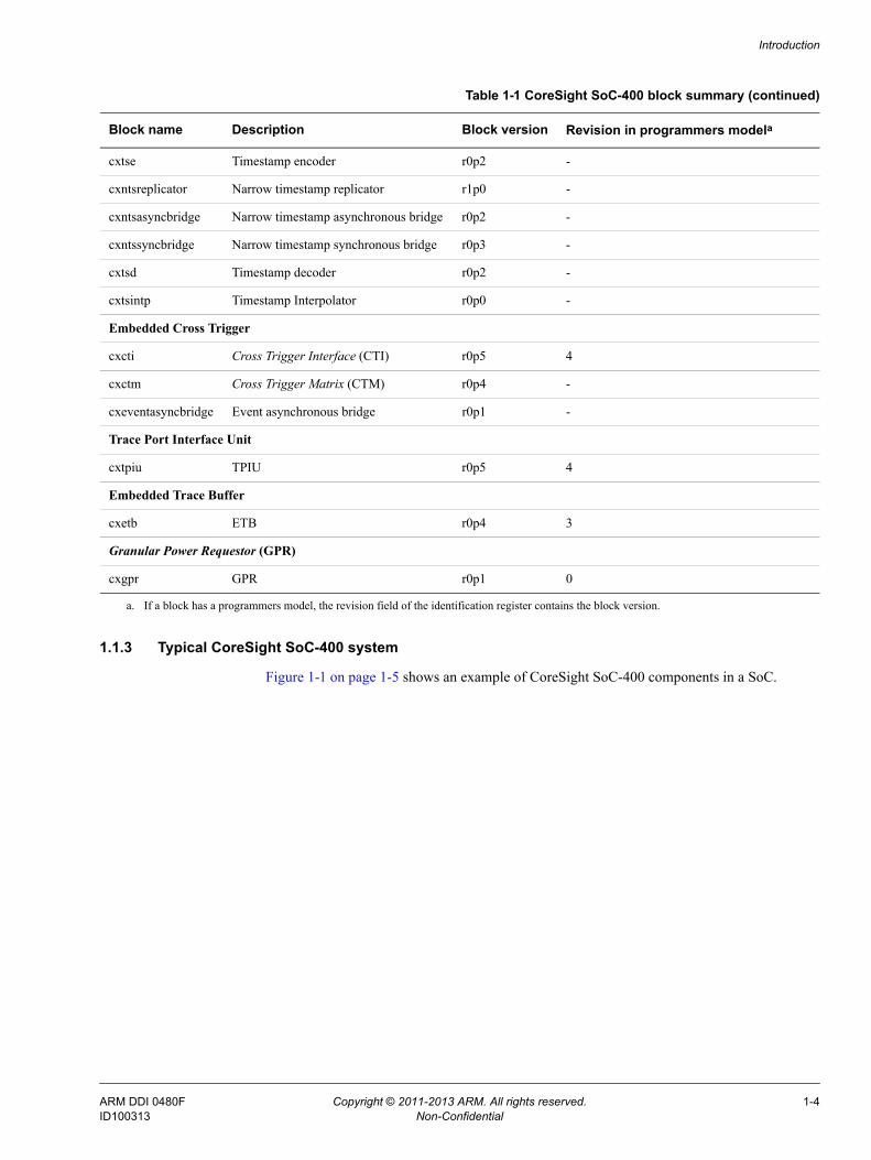
1.1.2 CoreSight SoC-400 block summary
Table 1-1 shows the CoreSight SoC-400 blocks and their current versions.
Table 1-1 CoreSight SoC-400 block summary
Block name Description Block version Revision in programmers modela
Authentication bridges
cxauthreplicator Authentication replicator r1p0 -
cxauthasyncbridge Authentication asynchronous bridge r1p0 -
cxauthsyncbridge Authentication synchronous bridge r1p0 -
Debug Access Port (DAP) blocks
cxdapahbap AHB access port r0p8 7
cxdapapbap APB access port r0p5 4
cxdapjtagap JTAG access port r0p3 2
cxdapasyncbridge DAPBUS asynchronous bridge r0p1 -
cxdapsyncbridge DAPBUS synchronous bridge r0p0 -
cxdapaxiap AXI access port r1p0 3
cxdapbusic DAPBUS interconnect r1p0 -
cxdapswjdp Serial wire and JTAG debug port:• DAPSWDP.• DAPJTAGDP.
-r1p4r1p4
-55
APB Interconnect components
cxapbic APB interconnect r0p1 -
cxapbasyncbridge APB asynchronous bridge r0p1 -
cxapbsyncbridge APB synchronous bridge r0p0 -
ATB Interconnect components
cxatbfunnel ATB funnel r1p0 2See ATB funnel register summary on page 3-30.
cxatbupsizer ATB upsizer r0p0 -
cxatbdownsizer ATB downsizer r0p0 -
cxatbasyncbridge ATB asynchronous bridge r0p1 -
cxatbsyncbridge ATB synchronous bridge r0p1 -
cxatbreplicator ATB replicator r0p0 1
Timestamp components
cxtsgen Timestamp generator r0p1 1See Timestamp generator register summary on page 3-203.
ARM DDI 0480F Copyright © 2011-2013 ARM. All rights reserved. 1-3ID100313 Non-Confidential
Introduction
1.1.3 Typical CoreSight SoC-400 system
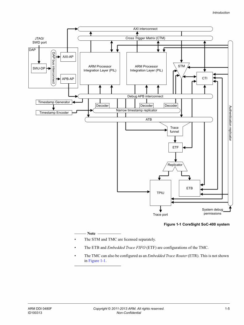
Figure 1-1 on page 1-5 shows an example of CoreSight SoC-400 components in a SoC.
cxtse Timestamp encoder r0p2 -
cxntsreplicator Narrow timestamp replicator r1p0 -
cxntsasyncbridge Narrow timestamp asynchronous bridge r0p2 -
cxntssyncbridge Narrow timestamp synchronous bridge r0p3 -
cxtsd Timestamp decoder r0p2 -
cxtsintp Timestamp Interpolator r0p0 -
Embedded Cross Trigger
cxcti Cross Trigger Interface (CTI) r0p5 4
cxctm Cross Trigger Matrix (CTM) r0p4 -
cxeventasyncbridge Event asynchronous bridge r0p1 -
Trace Port Interface Unit
cxtpiu TPIU r0p5 4
Embedded Trace Buffer
cxetb ETB r0p4 3
Granular Power Requestor (GPR)
cxgpr GPR r0p1 0
a. If a block has a programmers model, the revision field of the identification register contains the block version.
Table 1-1 CoreSight SoC-400 block summary (continued)
Block name Description Block version Revision in programmers modela
ARM DDI 0480F Copyright © 2011-2013 ARM. All rights reserved. 1-4ID100313 Non-Confidential
Introduction
Figure 1-1 CoreSight SoC-400 system
Note • The STM and TMC are licensed separately.
• The ETB and Embedded Trace FIFO (ETF) are configurations of the TMC.
• The TMC can also be configured as an Embedded Trace Router (ETR). This is not shown in Figure 1-1.
Tracefunnel
Replicator
ARM Processor Integration Layer (PIL)
STM
Trace port
ETF
Decoder DecoderTimestamp Generator
Timestamp Encoder
Decoder
AXI interconnect
Cross Trigger Matrix (CTM)
Debug APB interconnect
ATB
TPIU
Narrow timestamp replicator
Authentication replicator
ARM Processor Integration Layer (PIL)
CTI
ETB
System debug permissions
SWJ-DP
DA
P bus interconnect
JTAG/ SWD port
AXI-AP
APB-AP
DAP
ARM DDI 0480F Copyright © 2011-2013 ARM. All rights reserved. 1-5ID100313 Non-Confidential
Introduction
1.2 ComplianceCoreSight SoC-400 is compliant with the following specifications:
• Version 2 of the ARM® CoreSight™ Architecture Specification.
• Version 3 of the ARM® AMBA® APB Protocol Specification.
• ARM® AMBA® 4 ATB Protocol Specification ATBv1.0 and ATBv1.1.
• ARM® Debug Interface Architecture Specification, ADIv5.0 to ADIv5.2.
• ARM® AMBA2 AHB Specification.
• ARM®AMBA AXI4 Protocol Specification.
• IP-XACT version 1.4, defined by Accellera.
• IEEE 1149.1-2001 IEEE Standard Test Access Port and Boundary Scan Architecture(JTAG).
ARM DDI 0480F Copyright © 2011-2013 ARM. All rights reserved. 1-6ID100313 Non-Confidential

Introduction
1.3 FeaturesCoreSight SoC-400 has the following features:
• Access to debug features and on-chip AXI, AHB, APB, and JTAG buses through a JTAG or Single Wire Debug (SWD) interface.
• Merging of multiple trace sources into a single trace stream.
• Configurable trace bus widths between 8 bits and 128 bits, with upsizing and downsizing between different widths.
• Capture of trace streams on-chip or off-chip.
• Cross-triggering between different debug and trace components.
• Timestamp generation and system-wide compressed timestamp distribution, including local interpolation to provide local high-resolution timestamps synchronized to a global low-resolution timestamp.
• Support for inserting synchronous and asynchronous clock domain boundaries and power domain boundaries across internal interfaces.
• Improved configurability of components to better optimize area and power consumption.
• Integration with supported ARM processors.
• Integration of STM and TMC, licensed separately.• IP-XACT views of all components, defining interfaces, signals, and configurability and
programmers models.
• Power intent for all components in Unified Power Format (UPF), including definitions of how signals must be clamped when parts of the system are powered down.
• Synthesis flow.
• Flow to verify correct CoreSight system integration.
• Optional support for AMBA Designer, enabling graphical component configuration, system stitching, and verification.
• Full compliance with the CoreSight architecture, enabling integration of third-party IP and comprehensive tools support.
ARM DDI 0480F Copyright © 2011-2013 ARM. All rights reserved. 1-7ID100313 Non-Confidential

Introduction
1.4 InterfacesCoreSight SoC-400 provides the following interfaces for connection to the pins of a SoC:• JTAG and SWD, for debugger control, that share the same pins if they are both supported.• CoreSight Trace Port, for off-chip trace capture.
CoreSight SoC-400 provides the following interfaces for integration with non-CoreSight parts of the SoC:• AMBA AXI4.• AMBA 3 APB.• AMBA 2 AHB.• JTAG, for control of legacy on-chip JTAG debug components.• AMBA low-power interface.
CoreSight SoC-400 uses the following interfaces internally, which are used for communication between CoreSight components:
• AMBA APB3.
• AMBA ATB4.
• Event interface, for connecting trigger inputs and outputs to the CTI.
• Channel interface, for connecting CTIs to the CTM.
• Wide timestamp interface, for providing timestamps to components.
• Narrow timestamp interface, for efficient communication of the timestamp across the system.
• Authentication interface.
ARM DDI 0480F Copyright © 2011-2013 ARM. All rights reserved. 1-8ID100313 Non-Confidential

Introduction
1.5 Configurable options
See the ARM® CoreSight™ SoC-400 Integration Manual.
ARM DDI 0480F Copyright © 2011-2013 ARM. All rights reserved. 1-9ID100313 Non-Confidential

Introduction
1.6 Test featuresCoreSight SoC-400 has the following test features:
• MBIST interface for ETB RAM. See Embedded Trace Buffer on page 2-26.
ARM DDI 0480F Copyright © 2011-2013 ARM. All rights reserved. 1-10ID100313 Non-Confidential

Introduction
1.7 Product documentation and design flow
• For information about designing a debug and trace sub system, see the ARM® CoreSight™ SoC-400 System Design Guide (SDG) and the ARM® CoreSight™ Architecture Specification (AS).The SDG and the AS are confidential books that are only available to licensees.
• For information about the CoreSight components that CoreSight SoC-400 delivers, see this TRM.
• For instructions on how to configure and integrate the components, see the ARM® CoreSight™ SoC-400 Integration Manual (IM).The IM is a confidential book that is only available to licensees.
• For instructions on how to validate the debug and trace features of your design, see the ARM® CoreSight™ SoC-400 User Guide (UG).The UG is a confidential book that is only available to licensees.
• For instructions on how to perform synthesis on your CoreSight system, see the ARM® CoreSight™ SoC-400 Implementation Guide (IG).The IG is a confidential book that is only available to licensees.
The validation flow works with your existing SoC testbench. The validation modules, such as the cxdt, can be instantiated at the testbench level. This makes it possible to accommodate the validation flow without any modification to your SoC under test.
Figure 1-2 on page 1-12 shows how you can design, implement, and validate the debug and trace components in a SoC that contains one or more ARM processors.
ARM DDI 0480F Copyright © 2011-2013 ARM. All rights reserved. 1-11ID100313 Non-Confidential

Introduction
Figure 1-2 Design and validation workflow with CoreSight SoC-400
* Only when a PIL is required and the ARM processor deliverables do not include it** Trace macrocell and other CoreSight components, for example TMC or STM, are licensed separately from CoreSight SoC-400*** Only when a PIL is required
Install the PIL* and the trace macrocell** into the
processor deliverables
Configure the CoreSight SoC-400 components
Integrate the SoC, the Debug and Trace module, and the optional TPIU loggers to the testbench
Execute the test code in the testbench
Configurethe PIL***/processor
Connect the PIL/processorto the peripherals in the SoC
Integrate the CoreSight components into a debug and trace subsystem
Start
End
Changeyour
design
Design your SoC, your debug and trace subsystem, and your testbench
Can be done in AMBA Designer
Integrate the PIL/processor and the debug and trace subsystem into the SoC
Configure the other CoreSight components**
ARM DDI 0480F Copyright © 2011-2013 ARM. All rights reserved. 1-12ID100313 Non-Confidential

Introduction
1.8 Product revisionsThis section describes the differences in functionality between product revisions:
r0p0 First release.
r0p0-r1p0 Two new components added:• Granular Power Requestor. See Chapter 11 Granular Power Requestor.• Timestamp interpolator. See Timestamp interpolator on page 7-11.
r1p0-r2p0 r2p0 includes fixes for all known engineering errata relating to r1p0.
r2p0-r2p1 r2p1 includes fixes and IP-XACT changes.
r2p1-r3p0 r3p0 delivers• Test code written in C.• Example testbenches and example debug and trace sub systems.• Fixes and IP-XACT changes.
r3p0-r3p1 r3p1 delivers• Performance improvements to timestamp components.• Fixes and IP-XACT changes.
ARM DDI 0480F Copyright © 2011-2013 ARM. All rights reserved. 1-13ID100313 Non-Confidential

Chapter 2 Functional Overview
This chapter introduces the components available for building a CoreSight SoC-400 trace and debug infrastructure. It describes the basic function of each block and its I/O signals. The configurable parameters for each block are described.
This chapter contains the following sections:• DAP components on page 2-2.• APB components on page 2-9.• ATB interconnect components on page 2-12.• Timestamp components on page 2-19.• Embedded Cross Trigger components on page 2-24.• Trace sink components on page 2-26.• Authentication bridges on page 2-28.• Granular Power Requestor on page 2-30.
ARM DDI 0480F Copyright © 2011-2013 ARM. All rights reserved. 2-1ID100313 Non-Confidential

Functional Overview
2.1 DAP componentsThe DAP is a collection of components through which off-chip debug tools access a SoC. For more information about the DAP, see Chapter 4 Debug Access Port. It consists of the following components:• Serial Wire or JTAG Debug Port.• DAPBUS interconnect.• DAPBUS asynchronous bridge on page 2-3.• DAPBUS synchronous bridge on page 2-4.• JTAG access port on page 2-4.• AXI access port on page 2-5.• AHB access port on page 2-6.• APB access port on page 2-7.
2.1.1 Serial Wire or JTAG Debug Port
The Serial Wire or JTAG Debug Port (SWJ-DP) connects either a Serial Wire Debug or JTAG probe to the CoreSight SoC-400 debug system. This is the entry point into the debug infrastructure from the external debugger through the Debug Port (DP). Figure 2-1 shows the external connections on the SWJ-DP.
See Chapter 4 Debug Access Port.
Figure 2-1 SWJ-DP block diagram
2.1.2 DAPBUS interconnect
The DAPBUS interconnect connects a debug port to a configurable number of access ports.
The DAPBUS interconnect has the following key features:• Combinational interconnect.• Single power domain.• One slave interface port to connect to the DP.• Configurable number of master interfaces from 1-32.
SWJ-DP
dapclkdapclken
Clockandreset dapresetn
jtagtop
swdoswdoen
tdontdoen
ntrstnpotrst
swclktckswditms
tdi
dapprdata[31:0]
dapwrite
dapwdata[31:0]dapcaddr[15:2]
dapready
dapenabledapsel
dapslverrdapabort
DAPinternal master
jtagnsw
targetid[31:0]instanceid[3:0]
cdbgpwrupreq
csyspwrupackcsyspwrupreq
cdbgpwrupack
cdbgrstackcdbgrstreq
Debugpower onrequest
Systempower onrequest
Debugreset
request
JTAGcontrol
Serial Wireand
JTAGport
SWmultidrop
ARM DDI 0480F Copyright © 2011-2013 ARM. All rights reserved. 2-2ID100313 Non-Confidential

Functional Overview
Figure 2-2 shows the external connections on the DAPBUS interconnect. <x> is the interface number of the master port.
Figure 2-2 DAPBUS interconnect block diagram
2.1.3 DAPBUS asynchronous bridge
The DAPBUS asynchronous bridge enables data transfer between two asynchronous clock domains within the DAP sub system. The DAPBUS asynchronous bridge is designed to exist across two power domains and provides a Low-power Interface (LPI).
The DAPBUS asynchronous bridge has the following key features:• Configurable LPI.• Supports asynchronous clock domain crossing.• Configurable as one of the following blocks:
— A slave interface block.— A master interface block.— A full bridge including slave and master interfaces.
Figure 2-3 shows the external connections on the DAPBUS asynchronous bridge.
Figure 2-3 DAPBUS asynchronous bridge block diagram
DAPBUS interconnect
clk
daprdatas[31:0]
dapreadys
dapwrites
dapwdatas[31:0]
dapenablesdapsels
dapslverrs
Clockandreset
dapcaddrs[15:2]
dapaborts
Slaveaccess
port
resetn
dapprdatam<x>[31:0]
dapwritem<x>
dapwdatam<x>[31:0]dapcaddrm<x>[7:2]
dapreadym<x>
dapenablem<x>dapselm<x>
dapslverrm<x>dapabortm<x>
Examplemasteraccess
port
DAPBUS asynchronous bridge
Slaveinterface
daprdatas[31:0]
csysreq
dapreadys
cactive
daprdatam[31:0]
Masterinterface
dapwritesdapwdatas[31:0]
dapaddrs[31:0]
dapenables
dapabortsdapslverrs
csysack
dapwritemdapwdatam[31:0]dapaddrm[31:0]dapreadymdapenablem
dapselmdapslverrm
dapsels dapabortm
dapclks
dapresetsn
Clockandreset
dapclkm
dapresetmndapclkens dapclkenm
Lowpower
interface
Clockandreset
slave interface
master interface
ARM DDI 0480F Copyright © 2011-2013 ARM. All rights reserved. 2-3ID100313 Non-Confidential
Functional Overview
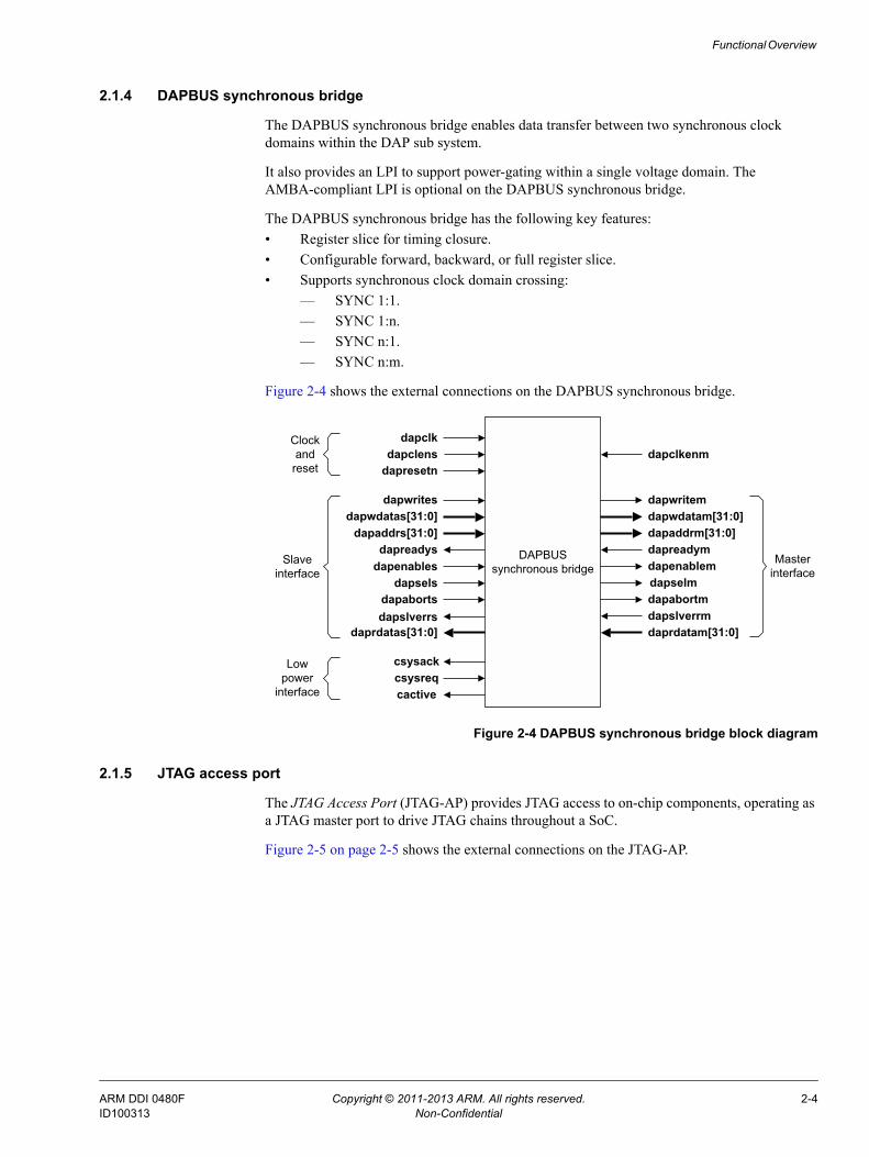
2.1.4 DAPBUS synchronous bridge
The DAPBUS synchronous bridge enables data transfer between two synchronous clock domains within the DAP sub system.
It also provides an LPI to support power-gating within a single voltage domain. The AMBA-compliant LPI is optional on the DAPBUS synchronous bridge.
The DAPBUS synchronous bridge has the following key features:• Register slice for timing closure.• Configurable forward, backward, or full register slice.• Supports synchronous clock domain crossing:
— SYNC 1:1.— SYNC 1:n.— SYNC n:1.— SYNC n:m.
Figure 2-4 shows the external connections on the DAPBUS synchronous bridge.
Figure 2-4 DAPBUS synchronous bridge block diagram
2.1.5 JTAG access port
The JTAG Access Port (JTAG-AP) provides JTAG access to on-chip components, operating as a JTAG master port to drive JTAG chains throughout a SoC.
Figure 2-5 on page 2-5 shows the external connections on the JTAG-AP.
DAPBUS synchronous bridge
dapclk
dapresetn
Clockandreset
dapclens
daprdatas[31:0]
dapsels
dapslverrs
dapwdatas[31:0]dapaddrs[31:0]
dapreadysdapenables
dapaborts
dapwrites
Slaveinterface
dapclkenm
dapreadymdapenablem
dapaddrm[31:0]dapwdatam[31:0]dapwritem
dapabortmdapslverrmdaprdatam[31:0]
dapselm
Masterinterface
csysackcsysreqcactive
Lowpower
interface
ARM DDI 0480F Copyright © 2011-2013 ARM. All rights reserved. 2-4ID100313 Non-Confidential

Functional Overview
Figure 2-5 JTAG Access Port block diagram
2.1.6 AXI access port
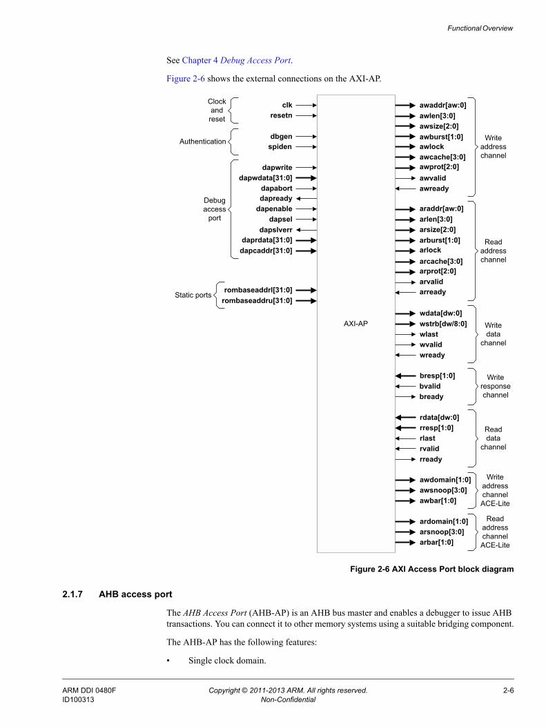
The AXI Access Port (AXI-AP) is an AXI bus master and enables a debugger to issue AXI transactions. You can connect it to other memory systems using a suitable bridging component.
The AXI-AP has the following features:
• Supports a single clock domain.
• Has a configurable 32-bit or 64-bit address width.
• Has a configurable 32-bit or 64-bit data width.
• Has AXI4 interface support for the following:— Large Physical Address Extension (LPAE).— Burst length of one.— No out-of-order transactions.— No multiple outstanding accesses except for barrier transactions.— No write data interleaving.— Only aligned transfers.— No EXCLUSIVE and LOCK transactions.— No QoS signaling.
• Has ACE-Lite support for system coherency as follows:— ReadOnce and WriteUnique support for shared memory regions.— ReadNoSnoop and WriteNoSnoop support for non-shared memory regions.— Synchronization and memory barrier transactions support.
• Is little-endian.
• Supports error responses.
• Supports packed transfers, enabling multiple 8-bit or 16-bit transfers to be issued with a single debugger access to the AXI-AP.
You must configure the AXI-AP during implementation, with the following parameters:• AXI_ADDR_WIDTH, 32-bit or 64-bit. See aw in Figure 2-6 on page 2-6.• AXI_DATA_WIDTH, 32-bit or 64-bit. See dw in Figure 2-6 on page 2-6.
JTAG-AP
daprdata[31:0]
dapready
dapwritedapwdata[31:0]
dapenabledapsel
dapaddr[7:2]
dapabortDebugaccess
port
dapclkdapclken
Clockandreset dapresetn
csrtck[7:0]srstconnected[7:0]portconnected[7:0]portenabled[7:0]cstdo[7:0]nsrstout[7:0]ncstrst[7:0]cstck[7:0]cstdi[7:0]cstms[7:0]
Connectionsto JTAG
slave
ARM DDI 0480F Copyright © 2011-2013 ARM. All rights reserved. 2-5ID100313 Non-Confidential
Functional Overview
See Chapter 4 Debug Access Port.
Figure 2-6 shows the external connections on the AXI-AP.
Figure 2-6 AXI Access Port block diagram
2.1.7 AHB access port
The AHB Access Port (AHB-AP) is an AHB bus master and enables a debugger to issue AHB transactions. You can connect it to other memory systems using a suitable bridging component.
The AHB-AP has the following features:
• Single clock domain.
AXI-AP
clkresetn
daprdata[31:0]
dapready
dapwritedapwdata[31:0]
dapenabledapsel
dapslverr
Clockandreset
dapcaddr[31:0]
dapabort
dbgenspiden
wdata[dw:0]
araddr[aw:0]arlen[3:0]arsize[2:0]arburst[1:0]arlock
arvalidarready
wstrb[dw/8:0]wlastwvalidwready
bresp[1:0]bvalidbready
rdata[dw:0]rresp[1:0]rlastrvalidrready
awdomain[1:0]awsnoop[3:0]awbar[1:0]
ardomain[1:0]arsnoop[3:0]arbar[1:0]
Writeaddresschannel
Readaddresschannel
Writedata
channel
Writeresponsechannel
Readdata
channel
WriteaddresschannelACE-Lite
ReadaddresschannelACE-Lite
Authentication
Debugaccess
port
awaddr[aw:0]awlen[3:0]awsize[2:0]awburst[1:0]awlock
awvalidawready
arcache[3:0]arprot[2:0]
awcache[3:0]awprot[2:0]
rombaseaddrl[31:0]rombaseaddru[31:0]
Static ports
ARM DDI 0480F Copyright © 2011-2013 ARM. All rights reserved. 2-6ID100313 Non-Confidential

Functional Overview
• Support for AMBA 2 AHB, ARM11 AHB extensions, and TrustZone extensions.
• Does not support the following AHB features:— BURST or SEQ transactions.— Exclusive accesses.— Unaligned transfers.
See Chapter 4 Debug Access Port.
Figure 2-7 shows the external connections on the AHB-AP.
Figure 2-7 AHB Access Port block diagram
2.1.8 APB access port
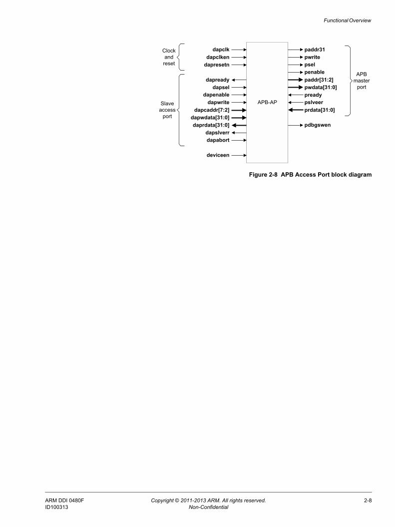
The APB Access Port (APB-AP) is an APB bus master and enables a debugger to issue APB transactions. This is normally used to control a dedicated CoreSight APB bus for programming CoreSight components.
The APB-AP has the following features:
• Single clock domain.
• AMBA 3 APB support.
• A 32-bit data bus. All transactions are 32 bits wide and are aligned to a 32-bit boundary.
• PADDR31 support for distinguishing between accesses from a debugger and on-chip debug software.
See Chapter 4 Debug Access Port.
Figure 2-8 on page 2-8 shows the external connections on the APB-AP.
AHB-AP
dapclk
dapresetn
daprdata[31:0]
dapready
dapwritedapwdata[31:0]
dapenabledapsel
dapslverr
Clockandreset
dapcaddr[7:2]
dapabort
dbgenspiden
hsizem[2:0]hburstm[2:0]
hprotm[6:0]haddrm[31:0]hwdatam[31:0]
hbstrbm[3:0]
AHBport
Authentication
Debugaccess
port
hreadym
hwritemhrdatam[31:0]
htransm[1:0]
hrespm
hlockm
dapclken
rombaseaddr[31:0] Static port
ARM DDI 0480F Copyright © 2011-2013 ARM. All rights reserved. 2-7ID100313 Non-Confidential
Functional Overview
Figure 2-8 APB Access Port block diagram
APB-AP
daprdata[31:0]
dapready
dapwrite
dapwdata[31:0]
dapenabledapsel
dapslverr
dapcaddr[7:2]
dapabort
Slaveaccess
port
dapclkClockandreset
dapclkendapresetn
deviceen
APBmaster
portpwdata[31:0]
pwrite
paddr[31:2]
pslveerpready
pselpenable
prdata[31:0]
paddr31
pdbgswen
ARM DDI 0480F Copyright © 2011-2013 ARM. All rights reserved. 2-8ID100313 Non-Confidential
Functional Overview
2.2 APB componentsThis section describes the components that are used to build a debug APB interconnect
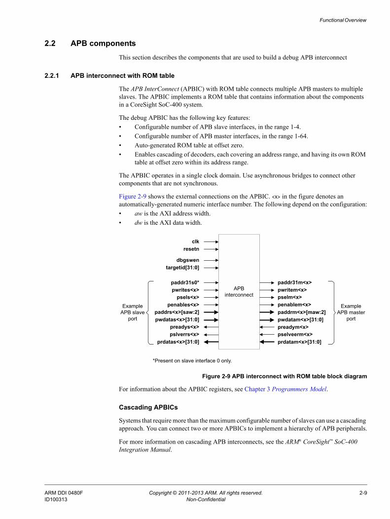
2.2.1 APB interconnect with ROM table
The APB InterConnect (APBIC) with ROM table connects multiple APB masters to multiple slaves. The APBIC implements a ROM table that contains information about the components in a CoreSight SoC-400 system.
The debug APBIC has the following key features:• Configurable number of APB slave interfaces, in the range 1-4.• Configurable number of APB master interfaces, in the range 1-64.• Auto-generated ROM table at offset zero.• Enables cascading of decoders, each covering an address range, and having its own ROM
table at offset zero within its address range.
The APBIC operates in a single clock domain. Use asynchronous bridges to connect other components that are not synchronous.
Figure 2-9 shows the external connections on the APBIC. <x> in the figure denotes an automatically-generated numeric interface number. The following depend on the configuration:• aw is the AXI address width.• dw is the AXI data width.
Figure 2-9 APB interconnect with ROM table block diagram
For information about the APBIC registers, see Chapter 3 Programmers Model.
Cascading APBICs
Systems that require more than the maximum configurable number of slaves can use a cascading approach. You can connect two or more APBICs to implement a hierarchy of APB peripherals.
For more information on cascading APB interconnects, see the ARM® CoreSight™ SoC-400 Integration Manual.
APB interconnect
ExampleAPB master
port
clk
dbgswen
pwrites<x>
prdatas<x>[31:0]
preadys<x>
Example APB slave
port
psels<x>penables<x>
paddrs<x>[saw:2]pwdatas<x>[31:0]
pslverrs<x>
resetn
targetid[31:0]
paddr31s0*
pwdatam<x>[31:0]
pwritem<x>
paddrm<x>[maw:2]
pselveerm<x>preadym<x>
pselm<x>penablem<x>
prdatam<x>[31:0]
paddr31m<x>
*Present on slave interface 0 only.
ARM DDI 0480F Copyright © 2011-2013 ARM. All rights reserved. 2-9ID100313 Non-Confidential

Functional Overview
2.2.2 APB asynchronous bridge
The APB asynchronous bridge enables data transfer between two asynchronous clock domains.
It is designed to exist across two power domains and provides an LPI.
The APB asynchronous bridge has the following key features:• Supports asynchronous clock domain crossing.• Configurable generation of only slave interface, or only master interface, or full blocks.• Configurable LPI.
Figure 2-10 shows the external connections to the APB asynchronous bridge.
Figure 2-10 APB asynchronous bridge block diagram
2.2.3 APB synchronous bridge
The APB synchronous bridge enables data transfer between two synchronous clock domains.
It also provides an LPI to support power-gating with a single voltage domain.
The APB synchronous bridge has the following key features:• Register slice for timing closure.• Configurable LPI.• Supports synchronous clock domain crossing:
— SYNC 1:1.— SYNC 1:n.— SYNC n:1.— SYNC n:m.
• Configurable forward, reverse, or full register slice.
Figure 2-11 on page 2-11 shows the external connections on the APB synchronous bridge.
APB asynchronousbridge
Slaveinterface
Masterinterface
presetsnClockandreset
pclks
pcklens
pwrites
prdatas[31:0]
preadys
csysreq
APBslaveport
pselspenables
paddrs[31:0]pwdatas[31:0]
pslverrs
csysack
cactive
Lowpower
interface
APBmaster
portpwdatam[31:0]
pwritem
paddrm[31:0]
pslverrmpreadym
pclkenm
pselmpenablem
prdatam[31:0]
pclkmpresetmn
Clockandreset
ARM DDI 0480F Copyright © 2011-2013 ARM. All rights reserved. 2-10ID100313 Non-Confidential

Functional Overview
Figure 2-11 APB synchronous bridge block diagram
APBsynchronous
bridge
pclkenm
paddrm[31:0]pwritempwdatam[31:0]pselmpenablempreadymprdatam[31:0]pslverrm
pclkpclkenspresetn
paddrs[31:0]pwrites
pwdatas[31:0]psels
penablespreadys
prdatas[31:0]pslverrs
csysackcsysreqcactive
Clockandreset
APBslaveport
Lowpower
interface
APBmaster
port
ARM DDI 0480F Copyright © 2011-2013 ARM. All rights reserved. 2-11ID100313 Non-Confidential

Functional Overview
2.3 ATB interconnect componentsThe ATB interconnect facilitates the transfer of trace data around the CoreSight SoC-400 debug system. A custom-generated interconnect infrastructure also uses these components to provide additional functionality as required by your system architecture:• ATB replicator.• ATB funnel on page 2-13.• ATB upsizer on page 2-14.• ATB downsizer on page 2-15.• ATB asynchronous bridge on page 2-16.• ATB synchronous bridge on page 2-17.
See Chapter 6 ATB Interconnect Components.
2.3.1 ATB replicator
The ATB replicator propagates data from a single master to two slaves at the same time.
The ATB replicator has the following key features:
• Configurable ATB data width.
• 1:2 replicator.
• Configurable APB programming interface to enable or disable interfaces and set up ID-based filtering.
The following parameter affects the signals of the ATB replicator:
• ATB_DATA_WIDTH, which has a value of 8, 16, 32, or 64. See dw in Figure 2-12 on page 2-13 where dw=ATB_DATA_WIDTH-1.
Figure 2-12 on page 2-13 shows the external connections on the ATB replicator.
ARM DDI 0480F Copyright © 2011-2013 ARM. All rights reserved. 2-12ID100313 Non-Confidential
Functional Overview
Figure 2-12 ATB replicator block diagram
Note In Figure 2-12, bw is generated automatically from the parameter ATB_DATA_WIDTH.
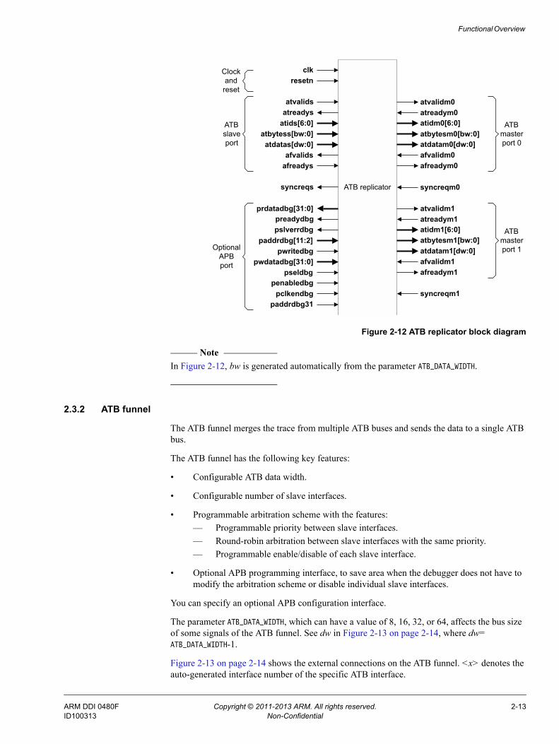
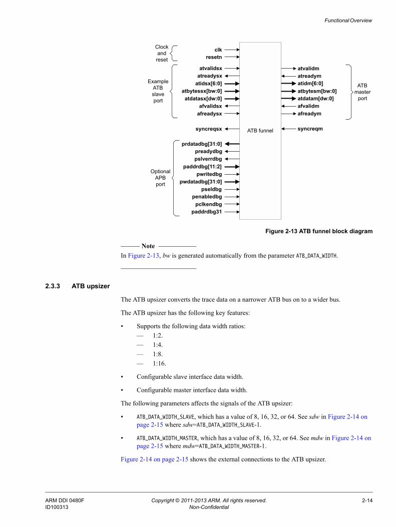
2.3.2 ATB funnel
The ATB funnel merges the trace from multiple ATB buses and sends the data to a single ATB bus.
The ATB funnel has the following key features:
• Configurable ATB data width.
• Configurable number of slave interfaces.
• Programmable arbitration scheme with the features:— Programmable priority between slave interfaces.— Round-robin arbitration between slave interfaces with the same priority.— Programmable enable/disable of each slave interface.
• Optional APB programming interface, to save area when the debugger does not have to modify the arbitration scheme or disable individual slave interfaces.
You can specify an optional APB configuration interface.
The parameter ATB_DATA_WIDTH, which can have a value of 8, 16, 32, or 64, affects the bus size of some signals of the ATB funnel. See dw in Figure 2-13 on page 2-14, where dw= ATB_DATA_WIDTH-1.
Figure 2-13 on page 2-14 shows the external connections on the ATB funnel. <x> denotes the auto-generated interface number of the specific ATB interface.
ATB replicator
clk
atidm0[6:0] ATBmasterport 0
Clockandreset
resetn
atids[6:0]
atdatas[dw:0]afvalids
atbytess[bw:0]
atreadysatvalids
afreadys
syncreqs
ATBslaveport atdatam0[dw:0]
atvalidm0
atbytesm0[bw:0]
atreadym0
afvalidm0afreadym0
syncreqm0
atidm1[6:0] ATBmasterport 1atdatam1[dw:0]
atvalidm1prdatadbg[31:0]atreadym1
afvalidm1afreadym1
syncreqm1
preadydbg
atbytesm1[bw:0]paddrdbg[11:2]pslverrdbg
pwdatadbg[31:0]pwritedbg
pseldbgpenabledbg
OptionalAPBport
pclkendbgpaddrdbg31
ARM DDI 0480F Copyright © 2011-2013 ARM. All rights reserved. 2-13ID100313 Non-Confidential
Functional Overview
Figure 2-13 ATB funnel block diagram
Note In Figure 2-13, bw is generated automatically from the parameter ATB_DATA_WIDTH.
2.3.3 ATB upsizer
The ATB upsizer converts the trace data on a narrower ATB bus on to a wider bus.
The ATB upsizer has the following key features:
• Supports the following data width ratios:— 1:2.— 1:4.— 1:8.— 1:16.
• Configurable slave interface data width.
• Configurable master interface data width.
The following parameters affects the signals of the ATB upsizer:
• ATB_DATA_WIDTH_SLAVE, which has a value of 8, 16, 32, or 64. See sdw in Figure 2-14 on page 2-15 where sdw=ATB_DATA_WIDTH_SLAVE-1.
• ATB_DATA_WIDTH_MASTER, which has a value of 8, 16, 32, or 64. See mdw in Figure 2-14 on page 2-15 where mdw=ATB_DATA_WIDTH_MASTER-1.
Figure 2-14 on page 2-15 shows the external connections to the ATB upsizer.
ATB funnel
clk
atidm[6:0] ATBmaster
port
Clockandreset resetn
atidsx[6:0]
atdatasx[dw:0]afvalidsx
atbytessx[bw:0]
atreadysxatvalidsx
afreadysx
ExampleATBslaveport atdatam[dw:0]
atvalidm
atbytesm[bw:0]
atreadym
afvalidmafreadym
syncreqmsyncreqsx
prdatadbg[31:0]preadydbg
paddrdbg[11:2]pslverrdbg
pwdatadbg[31:0]pwritedbg
pseldbgpenabledbg
OptionalAPBport
pclkendbgpaddrdbg31
ARM DDI 0480F Copyright © 2011-2013 ARM. All rights reserved. 2-14ID100313 Non-Confidential

Functional Overview
Figure 2-14 ATB upsizer block diagram
Note In Figure 2-14, sbw and mbw are generated automatically from the parameters ATB_DATA_WIDTH_SLAVE and ATB_DATA_WIDTH_MASTER, respectively.
2.3.4 ATB downsizer
The ATB downsizer converts the trace data on a wider ATB bus onto a narrower width bus.
The ATB downsizer has the following key features:
• Supports the following data width ratios:— 2:1.— 4:1.— 8:1.— 16:1.
• Configurable slave interface data width.
• Configurable master interface data width.
The following parameters affects the signals of the ATB downsizer:
• ATB_DATA_WIDTH_SLAVE, which has a value of 8, 16, 32, or 64. See sdw in Figure 2-14 where sdw=ATB_DATA_WIDTH_SLAVE-1.
• ATB_DATA_WIDTH_MASTER, which has a value of 8, 16, 32, or 64. See mdw in Figure 2-14 where mdw=ATB_DATA_WIDTH_MASTER-1.
Figure 2-15 on page 2-16 shows the external connections on the ATB downsizer.
ATB upsizer
clk
atidm[6:0] ATBmaster
port
Clockandreset resetn
atids[6:0]
atdatas[sdw:0]afvalids
atbytess[sbw:0]
atreadysatvalids
afreadys
ATBslaveport atdatam[mdw:0]
atvalidm
atbytesm[mbw:0]
atreadym
afvalidmafreadym
syncreqs syncreqm
ARM DDI 0480F Copyright © 2011-2013 ARM. All rights reserved. 2-15ID100313 Non-Confidential

Functional Overview
Figure 2-15 ATB downsizer block diagram
Note In Figure 2-15, sbw and mbw are generated automatically from the parameters ATB_DATA_WIDTH_SLAVE and ATB_DATA_WIDTH_MASTER, respectively.
2.3.5 ATB asynchronous bridge
The ATB asynchronous bridge enables data transfer between two asynchronous clock domains.The ATB asynchronous bridge is designed to exist across two power domains, and provides an LPI.
The ATB asynchronous bridge has the following key features:
• Supports asynchronous clock domain crossing.
• Configurable ATB data width.
• Configurable LPI.
• Configurable as one of the following:— A slave interface block.— A master interface block.— A full bridge.
The following parameter affects the signals of the ATB asynchronous bridge:
• ATB_DATA_WIDTH, which has a value of 8, 16, 32, or 64. See dw in Figure 2-16 on page 2-17 where dw=ATB_DATA_WIDTH-1.
Figure 2-16 on page 2-17 shows the external connections to the ATB asynchronous bridge.
ATB downsizer
clk
atidm[6:0] ATBmaster
port
Clockandreset resetn
atids[6:0]
atdatas[sdw:0]afvalids
atbytess[sbw:0]
atreadysatvalids
afreadys
ATBslaveport atdatam[mdw:0]
atvalidm
atbytesm[mbw:0]
atreadym
afvalidmafreadym
syncreqs syncreqm
ARM DDI 0480F Copyright © 2011-2013 ARM. All rights reserved. 2-16ID100313 Non-Confidential

Functional Overview
Figure 2-16 ATB asynchronous bridge block diagram
Note In Figure 2-16, bw is generated automatically from the parameter ATB_DATA_WIDTH.
2.3.6 ATB synchronous bridge
The ATB synchronous bridge enables data transfer between two synchronous clock domains.It also provides an LPI to support power-gating with a single voltage domain.
The ATB synchronous bridge has the following key features:
• Configurable ATB data width.
• Configurable forward, backward, or full register slice.
• Supports synchronous clock domain crossing:— SYNC 1:1.— SYNC 1:n.— SYNC n:1.— SYNC n:m.
• Configurable FIFO depth in powers of 2 with a maximum depth of 256, when the bridge type is set to FULL. This can be used to implement a small trace FIFO, as an alternative to implementing an ETF.
• Configurable LPI.
The following parameter affects the signals of the ATB synchronous bridge:
ATB_DATA_WIDTH, which has a value of 8, 16, 32, or 64. See dw in Figure 2-17 on page 2-18 where dw=ATB_DATA_WIDTH-1.
Figure 2-17 on page 2-18 shows the external connections to the ATB synchronous bridge.
ATB asynchronousbridge
Slaveinterface
Masterinterface
Clockandreset clkens
atids[6:0]
atdatas[dw:0]afvalids
atbytess[bw:0]
atreadysatvalids
afreadys
ATBslaveport
resetsnclks
syncreqs
atidm[6:0]ATB
masterport
resetmn
atdatam[dw:0]
atvalidm
atbytesm[bw:0]
atreadym
afvalidmafreadymsyncreqm
csysreqcsysack
clkmclkenm
Clockandreset
Lowpower
interfacecactive
ARM DDI 0480F Copyright © 2011-2013 ARM. All rights reserved. 2-17ID100313 Non-Confidential

Functional Overview
Figure 2-17 ATB synchronous bridge block diagram
Note In Figure 2-17, bw is generated automatically from the parameter ATB_DATA_WIDTH.
ATBsynchronous
bridge
resetn
atidm[6:0] ATBmaster
port
Clockandreset
cactive
clkclkens clkenm
atids[6:0]
atdatas[dw:0]afvalids
atbytess[bw:0]
atreadysatvalids
afreadys
syncreqs
ATBslaveport atdatam[dw:0]
atvalidm
atbytesm[bw:0]
atreadym
afvalidmafreadym
syncreqm
csysreqcsysack
Lowpower
interface
ARM DDI 0480F Copyright © 2011-2013 ARM. All rights reserved. 2-18ID100313 Non-Confidential

Functional Overview
2.4 Timestamp componentsThe timestamp components generate and distribute a consistent timestamp value for multiple processors and other blocks within a SoC. The components available to build this system are:• Timestamp generator.• Timestamp encoder on page 2-20.• Narrow timestamp replicator on page 2-20.• Narrow timestamp asynchronous bridge on page 2-21.• Narrow timestamp synchronous bridge on page 2-21.• Timestamp decoder on page 2-22.• Timestamp interpolator on page 2-22.
See Chapter 7 Timestamp Components.
2.4.1 Timestamp generator
The timestamp generator generates a timestamp value that provides a consistent view of time for multiple processors and other blocks in a SoC.
You can also use the timestamp generator to generate a counter value that is compliant with the ARM Generic Timer specification for a memory-mapped counter module. For information on the ARM Generic Timer, see the relevant ARM Architecture Reference Manual.
The timestamp generator has the following key features:
• 64 bits wide to avoid roll-over issues.
• Starts from zero or a programmable value.
• A control APB interface enables the timer to be saved and restored across powerdown events.
• A read-only APB interface enables the timer value to be read by non-secure software and debug tools.
• Input to stop the timer value incrementing during full-system debug.
For more information on the timestamp generator, see Chapter 7 Timestamp Components.
For information on the timestamp generator register description, see Timestamp generator register summary on page 3-203.
Figure 2-18 on page 2-20 shows the external connections on the timestamp generator.
ARM DDI 0480F Copyright © 2011-2013 ARM. All rights reserved. 2-19ID100313 Non-Confidential

Functional Overview
Figure 2-18 Timestamp generator block diagram
2.4.2 Timestamp encoder
The timestamp encoder converts the 64-bit timestamp value from the timestamp generator to a 7-bit encoded value. This is called a narrow timestamp. It also encodes and sends the timestamp value over a 2-bit synchronization channel.
Figure 2-19 shows the external connections on the timestamp encoder.
Figure 2-19 Timestamp encoder block diagram
2.4.3 Narrow timestamp replicator
The narrow timestamp replicator distributes the encoded timestamp and synchronization data to multiple master interfaces. You can configure the number of master interfaces.
The narrow timestamp replicator has the following key features:• 1:n distribution of narrow timestamp bus.• Configurable number of narrow timestamp master interfaces.
Figure 2-20 on page 2-21 shows the external connections on the narrow timestamp replicator.
Timestamp generator
tsvalueb[63:0]
ControlAPB3
interface Widetimestampinterfacetsforcesync
ReadAPB3
interface
clkresetn
hltdbg
paddrctrl[11:2]pselctrl
penablectrlpwritectrl
pwdatactrl[31:0]preadyctrl
prdatactrl[31:0]psvlerrctrl
paddrread[11:2]pselread
penablereadpwriteread
pwdataread[31:0]preadyread
prdataread[31:0]pslverrread
Clockandreset
Timestamp encoder
tsclktsresetn
tsforcesync
tsbit[6:0]tssync[1:0]
tssyncready
tsvalue[63:0]
Narrowtimestampinterface
Wide timestampinterface
Clockandreset
ARM DDI 0480F Copyright © 2011-2013 ARM. All rights reserved. 2-20ID100313 Non-Confidential

Functional Overview
Figure 2-20 Narrow timestamp replicator block diagram
2.4.4 Narrow timestamp asynchronous bridge
The narrow timestamp asynchronous bridge enables the transfer of timestamp information across different clock and power domains.
The narrow timestamp asynchronous bridge has the following key features:• Supports asynchronous clock domain crossing.• LPI, that is not configurable.
Figure 2-21 shows the external connections on the narrow timestamp asynchronous bridge.
Figure 2-21 Narrow timestamp asynchronous bridge block diagram
2.4.5 Narrow timestamp synchronous bridge
The narrow timestamp synchronous bridge enables the transfer of timestamp information across clock and power domains that have individual clock enables.
The narrow timestamp synchronous bridge has the following key features:
• LPI, that is not configurable.
• Supports synchronous clock domain crossing:— SYNC 1:1.— SYNC 1:n.— SYNC n:1.— SYNC n:m.
clkresetn
tsbitmn[6:0]tssyncmn[1:0]tssyncreadymn
Example narrow
timestampinterface
Narrowtimestampinterface
Narrow timestamp replicator
tsbits[6:0]tssyncs[1:0]
tssyncreadys
Clockandreset
Narrow timestamp asynchronous bridge
Slaveinterface
clksresetsn
Narrowtimestampinterface
tsbits[6:0]tssyncs[1:0]
tssyncreadys
csysreqcsysackcactive
Lowpower
interface
tsbitm[6:0]tssyncm[1:0]tssyncreadym
Narrow timestampinterface
clkmresetmn
Masterinterface
Clockandreset
Clockandreset
ARM DDI 0480F Copyright © 2011-2013 ARM. All rights reserved. 2-21ID100313 Non-Confidential

Functional Overview
Figure 2-22 shows the external connections on the narrow timestamp synchronous bridge.
Figure 2-22 Narrow timestamp synchronous bridge block diagram
2.4.6 Timestamp decoder
The timestamp decoder converts the narrow timestamp interface and synchronization data back to a 64-bit value. This is the format in which the CoreSight SoC-400 trace components require their timestamp. It decodes the narrow timestamp interface to a 64-bit wide timestamp signal.
Figure 2-23 shows the external connections on the timestamp decoder.
Figure 2-23 Timestamp decoder block diagram
2.4.7 Timestamp interpolator
CoreSight SoC-400 components require timestamp values that allow software to correlate events. A timestamp generator generates timestamp values. This is typically at a clock rate that is much slower than the operating frequency of CoreSight SoC-400 components. The timestamp interpolator uses the timestamp values from the timestamp generator as reference and generates timestamp values at a rate required by CoreSight SoC-400 components.
The timestamp interpolator has the following key features:• Configurable ratio of SCLK base frequency to SCLK minimum frequency.• Configurable ratio of FCLK maximum frequency to SCLK base frequency.• Single clock domain operation.• Supports dynamic variation in clock frequencies.
SCLK This is the slow clock on which the timestamp generator operates. SCLK is the clk port on the timestamp generator.
FCLK This is the fast local clock on which the timestamp interpolator operates. FCLK is the clk port on the timestamp interpolator.
Figure 2-24 on page 2-23 shows the external connections on the timestamp interpolator.
Narrow timestamp
synchronous bridge
clkresetn
Narrowtimestampinterface
tsbits[6:0]tssyncs[1:0]
tssyncreadys
csysreqcsysackcactive
Low-power
interface
tsbitm[6:0]tssyncm[1:0]tssyncreadym
Narrow timestampinterface
clkenm
clkens
Clockandreset
Timestamp decoder
clkresetn
tsbit[6:0]tssync[1:0]
tssyncready
tsvalue[63:0]Narrow
timestampinterface
Clockandreset
Timestampinterface
ARM DDI 0480F Copyright © 2011-2013 ARM. All rights reserved. 2-22ID100313 Non-Confidential

Functional Overview
Figure 2-24 Timestamp interpolator block diagram
Timestamp interpolator
clkresetn
tsvalueintpb[63:0]tsvalueb[63:0]
Clockandreset
Timestampslave interface
Timestampmaster interface
ARM DDI 0480F Copyright © 2011-2013 ARM. All rights reserved. 2-23ID100313 Non-Confidential

Functional Overview
2.5 Embedded Cross Trigger componentsCoreSight SoC-400 contains the following cross-trigger components to control the logging of debug information:• Cross Trigger Interface.• Cross Trigger Matrix.• Event asynchronous bridge on page 2-25.
The CTI, CTM, and Event asynchronous bridge form the ECT sub-system that passes debug events from one debug component to another. For example, the ECT can communicate debug state information from one processor to the others so that you can stop the program execution on one or more processors at the same time if required.
2.5.1 Cross Trigger Interface
The CTI combines and maps the trigger requests, and broadcasts them to all other interfaces on the ECT sub system. When the CTI receives a trigger request it maps this onto a trigger output. This enables the CoreSight sub systems to cross trigger with each other. Figure 2-25 shows the external connections on the CTI.
Figure 2-25 Cross Trigger Interface block diagram
2.5.2 Cross Trigger Matrix
The CTM block distributes the trigger events. It connects to at least two CTIs and to other CTMs where required in a design. Figure 2-26 on page 2-25 shows the external connections on the CTM block.
Cross Trigger Interface (CTI)
pclkdbgpclkendbg
presetdbgn
APB clockand reset
cticlkcticlken
ctiresetn
Block clockand reset
Authentication interface
dbgenniden
Generalcontrol asicctl[7:0]
Syncbypass
ctiapbsbypasscisbypass
tisbypassin[7:0]tisbypassack[7:0]
ctitrigout[7:0]Trigger
interfacectitriginack[7:0]
ctitrigin[7:0]ctitrigoutack[7:0]
Channelinterfacectichout[3:0]
ctichinack[3:0]
ctichin[3:0]ctichoutack[3:0]
prdatadbg[31:0]preadydbg
paddrdbg[11:2]
pwdatadbg[31:0]pwritedbg
pseldbgpenabledbg
APBinterface
paddrdbg31Handshakebypass
cihsbypass[3:0]tihsbypass[7:0]
Debugenable
masking
tinidensel[7:0]todbgensel[7:0]
se Test
ARM DDI 0480F Copyright © 2011-2013 ARM. All rights reserved. 2-24ID100313 Non-Confidential

Functional Overview
Figure 2-26 Cross Trigger Matrix block diagram
2.5.3 Event asynchronous bridge
The event asynchronous bridge is a fixed component that synchronizes events on a single channel from the slave domain to the master domain. The event acknowledge from the master domain is synchronized and presented to the slave domain.
If the event is a pulse, the bridge internally stretches the event until it receives an acknowledge from the master domain. In this mode of operation, additional events from the slave domain are ignored until the acknowledge is received at the slave domain.
Figure 2-27 shows the external connections on the event asynchronous bridge.
Figure 2-27 Event asynchronous bridge block diagram
ctmclkctmclken
ctmresetn
Cross Trigger Matrix (CTM)
Channelinterface 0ctmchout0[3:0]
ctmchinack0[3:0]
ctmchin0[3:0]ctmchoutack0[3:0]
cisbypass0
se
Syncbypass
Handshakebypass
cihsbypass0[3:0]
cisbypass1cisbypass2cisbypass3
cihsbypass1[3:0]cihsbypass2[3:0]cihsbypass3[3:0]
Channelinterface 1ctmchout1[3:0]
ctmchinack1[3:0]
ctmchin1[3:0]ctmchoutack1[3:0]
Channelinterface 2ctmchout2[3:0]
ctmchinack2[3:0]
ctmchin2[3:0]ctmchoutack2[3:0]
Channelinterface 3ctmchout3[3:0]
ctmchinack3[3:0]
ctmchin3[3:0]ctmchoutack3[3:0]
Clockandreset
Event asynchronous bridge
Slaveinterface
Masterinterface
clksSlaveclockandreset
clkens
eventsEventslaveport eventacks
resetsn
Eventmaster
port
eventmeventackm
clkmclkenm
Masterclockandresetresetmn
ARM DDI 0480F Copyright © 2011-2013 ARM. All rights reserved. 2-25ID100313 Non-Confidential

Functional Overview
2.6 Trace sink componentsCoreSight SoC-400 contains the following components that receive debug information and forward it to the main debug infrastructure. The trace sink components are:• Trace Port Interface Unit.• Embedded Trace Buffer.
2.6.1 Trace Port Interface Unit
The TPIU connects an ATB to an external trace port. Figure 2-28 shows the external connections on the TPIU.
Figure 2-28 Trace Port Interface Unit block diagram
2.6.2 Embedded Trace Buffer
The ETB stores trace data in an on-chip RAM for later inspection by debug tools. The trace data buffer RAM size is configurable.
Figure 2-29 on page 2-27 shows the external connections of the ETB. In Figure 2-29 on page 2-27, aw is the highest order bit of the RAM address bus, and is dependent on the configured RAM size.
Trace Port Interface Unit
(TPIU)
atclkTrace busclock
and resetatclken
atids[6:0]
atdatas[31:0]afvalids
atbytess[1:0]
atreadys atvalids
afreadys
ATBslave port
prdatadbg[31:0]preadydbg paddrdbg[11:2]
pwdatadbg[31:0]pwritedbg
pseldbg penabledbg
APBprogramming
port
paddrdbg31
extctlin[7:0]
trigintriginack
flushin flushinack
Triggerand
flushing
atresetn
se
pclkdbgAPB clockandreset
pclkendbgpresetdbgn
Trace output
extctlout[7:0]
tpctlTie-offconfiguration
pins tpmaxdatasize[4:0]
traceclkinTrace sourceclock and
reset tresetn
tracedata[31:0]tracectltraceclk
ARM DDI 0480F Copyright © 2011-2013 ARM. All rights reserved. 2-26ID100313 Non-Confidential

Functional Overview
Figure 2-29 Embedded Trace Buffer block diagram
Embedded Trace Buffer
(ETB)
atclkClockandreset
atclken
atids[6:0]
atdatas[31:0]afvalids
atbytess[1:0]
atreadysatvalids
afreadys
ATBslaveport
prdatadbg[31:0]preadydbgpaddrdbg[11:2]
pwdatadbg[31:0]pwritedbg
pseldbgpenabledbg
APBprogramming
port
paddrdbg31
fullacqcomp
trigintriginack
flushinflushinack
Cross-triggering events
atresetn
se
pclkdbgAPBclockandreset
pclkendbgpresetdbgn
mbistdout[31:0]
mtestonmbistcembistwembistaddr[AW:0]mbistdin[31:0]
MBIST interface
ARM DDI 0480F Copyright © 2011-2013 ARM. All rights reserved. 2-27ID100313 Non-Confidential

Functional Overview
2.7 Authentication bridgesThe additional bridges are:• Authentication replicator.• Authentication asynchronous bridge.• Authentication synchronous bridge on page 2-29.
The authentication bridges provide authenticated debug control links in security-enabled CoreSight SoC-400 systems. These components are not required if this security is not required.
2.7.1 Authentication replicator
The authentication replicator enables the transfer of authentication signals from one master to multiple slaves.
The authentication replicator has the following key features:• Configurable for specific authentication signals.• Configurable for a number of authentication masters.
Figure 2-30 shows the external connections on the authentication replicator.
Figure 2-30 Authentication replicator block diagram
2.7.2 Authentication asynchronous bridge
The authentication asynchronous bridge enables transfer of authentication signals between two asynchronous clock domains.
The authentication asynchronous bridge has the following key features:• Configurable for specific authentication signals.• Supports asynchronous clock domain crossing.
Figure 2-31 on page 2-29 shows the external connections on the authentication asynchronous bridge.
Authentication replicator
clk
resetn
nidens
dbgens
spidens
spnidens
dbgswens
dbgenm<x>
nidenm<x>
spidenm<x>
spnidenm<x>
dbgswenm<x>
Clockandreset
Example authentication master interface
Authentication slave interface
ARM DDI 0480F Copyright © 2011-2013 ARM. All rights reserved. 2-28ID100313 Non-Confidential

Functional Overview
Figure 2-31 Authentication asynchronous bridge block diagram
2.7.3 Authentication synchronous bridge
The authentication synchronous bridge enables the transfers of authentication signals between two synchronous clock domains. It can also be used as a register slice to break long timing paths.
The authentication synchronous bridge has the following key features:• Configurable for specific authentication signals.• Register slice for timing closure.
Figure 2-32 shows the external connections on the authentication synchronous bridge.
Figure 2-32 Authentication synchronous bridge block diagram
Authentication asynchronousbridge
Slaveinterface
Masterinterface
resetsn
Clockandreset
clks
nidensdbgens
Slaveport spidens
spnidensdbgswens
Masterport
dbgenmnidenmspidenmspnidenmdbgswenm
resetmnclkm Clock
andreset
Authentication synchronous
bridge
resetn
Masterport
Clockandreset
clk
nidensdbgens
Slaveport
dbgenm
spidensspnidens
dbgswens
nidenmspidenmspnidenmdbgswenm
ARM DDI 0480F Copyright © 2011-2013 ARM. All rights reserved. 2-29ID100313 Non-Confidential

Functional Overview
2.8 Granular Power RequestorThe GPR enables a debugger to control powerup and powerdown of specific components within a debug and trace sub system. Without the GPR, the CoreSight DAP components only support system level powerup and powerdown of the entire CoreSight system. The finer granularity provided by the GPR enables implementation of power strategies during both debug and ATPG testing.
The GPR has a configurable number of power-control interfaces, up to 32. Synchronizers are implemented on the cpwrupack input signals, enabling the power-control interfaces to connect to components in a different clock domain.
Figure 2-33 shows the external connections on the GPR.
You must configure the GPR during implementation with the following parameters:• NUM_CPWRUPM. See Figure 2-33.
Figure 2-33 Granular Power Requestor block diagram
Granular Power
Requestor (GPR)
cpwrupreq[NUM_CPWRUPM-1:0]
cpwrupack[NUM_CPWRUPM-1:0]
clkresetn
penabledbgpwritedbg
paddrdbg[11:2]
pwdatadbg[31:0]pslverrdbgpreadydbg
prdatadbg[31:0]
pseldbg
paddrdbg31APB
controlinterface
Systempower onrequest
Clockandreset
ARM DDI 0480F Copyright © 2011-2013 ARM. All rights reserved. 2-30ID100313 Non-Confidential

Chapter 3 Programmers Model
This chapter describes the programmers model for the CoreSight SoC-400 components. It contains the following sections:• About the programmers model on page 3-2.• Granular Power Requestor register summary on page 3-3.• Granular Power Requestor register descriptions on page 3-4.• APB interconnect register summary on page 3-22.• APB interconnect register descriptions on page 3-23.• ATB funnel register summary on page 3-30.• ATB funnel register descriptions on page 3-31.• ATB replicator register summary on page 3-52.• ATB replicator register descriptions on page 3-53.• ETB register summary on page 3-69.• ETB register descriptions on page 3-71.• TPIU register summary on page 3-97.• TPIU register descriptions on page 3-99.• CTI register summary on page 3-135.• CTI register descriptions on page 3-137.• DAP register summary on page 3-171.• DAP register descriptions on page 3-175.• Timestamp generator register summary on page 3-203.• Timestamp generator registers description on page 3-205.
ARM DDI 0480F Copyright © 2011-2013 ARM. All rights reserved. 3-1ID100313 Non-Confidential

Programmers Model
3.1 About the programmers modelThis section describes register information for the CoreSight SoC-400 components.
The following applies to all the CoreSight SoC-400 register descriptions:
• All CoreSight SoC component registers are 32 bits wide.
• The base address is not fixed, and can be different for any particular system implementation. The offset of each register from the base address is fixed.
• Do not attempt to access reserved or unused address locations. Attempting to access these locations can result in UNPREDICTABLE behavior.
• Unless otherwise stated in the accompanying text:— Do not modify UNDEFINED register bits.— Ignore UNDEFINED register bits on a read operation.— A system or powerup reset resets all register bits to 0.
• Access types are described as follows:RW Read and write.RO Read-only.WO Write-only.SBZ Should-Be-Zero.SBZP Should-Be-Zero-or-Preserved.RAZ Read-As-Zero.RAZ/WI Read-As-Zero, Writes Ignored.
ARM DDI 0480F Copyright © 2011-2013 ARM. All rights reserved. 3-2ID100313 Non-Confidential

Programmers Model
3.2 Granular Power Requestor register summaryTable 3-1 shows the GPR registers in offset order from the base memory address.
Table 3-1 cxgpr register summary
Offset Name Type Reset Description
0x000 CPWRUPREQ RW 0x00000000 Debug Power Request register on page 3-4
0x004 CPWRUPACK RO 0x00000000 Debug Power Acknowledge register on page 3-7
0xF00 ITCTRL RO 0x00000000 Integration Mode Control register on page 3-9
0xFA0 CLAIMSET RW 0x0000000F Claim Tag Set register on page 3-10
0xFA4 CLAIMCLR RW 0x00000000 Claim Tag Clear register on page 3-11
0xFB0 LAR WO 0x00000000 Lock Access Register on page 3-11
0xFB4 LSR RO 0x00000003 Lock Status Register on page 3-12
0xFB8 AUTHSTATUS RO 0x00000000 Authentication Status register on page 3-13
0xFBC DEVARCH RO 0x00000000 Device Architecture register on page 3-13
0xFC8 DEVID RO 0x00000001 Device Configuration register on page 3-14
0xFCC DEVTYPE RO 0x00000034 Device Type Identifier register on page 3-15
0xFD0 PIDR4 RO 0x00000004 Peripheral ID4 Register on page 3-15
0xFD4 - - Reserved
0xFD8 - - Reserved
0xFDC - - Reserved
0xFE0 PIDR0 RO 0x000000A4 Peripheral ID0 Register on page 3-16
0xFE4 PIDR1 RO 0x000000B9 Peripheral ID1 Register on page 3-17
0xFE8 PIDR2 RO 0x0000000B Peripheral ID2 Register on page 3-17
0xFEC PIDR3 RO 0x00000000 Peripheral ID3 Register on page 3-18
0xFF0 CIDR0 RO 0x0000000D Component ID0 Register on page 3-18
0xFF4 CIDR1 RO 0x00000090 Component ID1 Register on page 3-19
0xFF8 CIDR2 RO 0x00000005 Component ID2 Register on page 3-20
0xFFC CIDR3 RO 0x000000B1 Component ID3 Register on page 3-20
ARM DDI 0480F Copyright © 2011-2013 ARM. All rights reserved. 3-3ID100313 Non-Confidential

Programmers Model
3.3 Granular Power Requestor register descriptionsThis section describes the GPR registers. Table 3-1 on page 3-3 provides cross-references to individual registers.
3.3.1 Debug Power Request register
The CPWRUPREQ register characteristics are:
Purpose Controls the values of the cpwrupreq outputs from the GPR. Each bit in this register controls the corresponding output on the cpwrupreq port. GPR contains hardware logic to ensure that the 4-phase handshake is not violated on the CPWRUP interfaces.When GPR asserts a powerup request that is not acknowledged, that is, cpwrupreq[n] = 1 and cpwrupack[n] = 0, writing a 0 to the CPWRUPREQ register bit[n] does not affect the cpwrupreq[n] output. Similarly, when GPR sends a powerdown request that is not acknowledged, that is, cpwrupreq[n] is 0 and cpwrupack[n] = 1, writing a 1 to the CPWRUPREQ register bit[n] does not affect the cpwrupreq[n] output.
Usage constraints There are no usage constraints.
Configurations This register is available in all configurations.
Attributes See the register summary in Table 3-1 on page 3-3.
There is a one to one mapping between the register locations and the CPWRUPREQ bits.
Table 3-2 shows the bit assignments.
Table 3-2 CPWRUPREQ register bit assignments
Bits Name Function
[31] CPWRUPREQBit31 Bit[31] of the cpwrupreq output port.0 Drive 0 on cpwrupreq[31] output port.1 Drive 1 on cpwrupreq[31] output port.
[30] CPWRUPREQBit30 Bit[30] of the cpwrupreq output port:0 Drive 0 on cpwrupreq[30] output port.1 Drive 1 on cpwrupreq[30] output port.
[29] CPWRUPREQBit29 Bit[29] of the cpwrupreq output port:0 Drive 0 on cpwrupreq[29] output port.1 Drive 1 on cpwrupreq[29] output port.
[28] CPWRUPREQBit28 Bit[28] of the cpwrupreq output port:0 Drive 0 on cpwrupreq[28] output port.1 Drive 1 on cpwrupreq[28] output port.
[27] CPWRUPREQBit27 Bit[27] of the cpwrupreq output port:0 Drive 0 on cpwrupreq[27] output port.1 Drive 1 on cpwrupreq[27] output port.
[26] CPWRUPREQBit26 Bit[26] of the cpwrupreq output port:0 Drive 0 on cpwrupreq[26] output port.1 Drive 1 on cpwrupreq[26] output port.
ARM DDI 0480F Copyright © 2011-2013 ARM. All rights reserved. 3-4ID100313 Non-Confidential

Programmers Model
[25] CPWRUPREQBit25 Bit[25] of the cpwrupreq output port:0 Drive 0 on cpwrupreq[25] output port.1 Drive 1 on cpwrupreq[25] output port.
[24] CPWRUPREQBit24 Bit[24] of the cpwrupreq output port:0 Drive 0 on cpwrupreq[24] output port.1 Drive 1 on cpwrupreq[24] output port.
[23] CPWRUPREQBit23 Bit[23] of the cpwrupreq output port:0 Drive 0 on cpwrupreq[23] output port.1 Drive 1 on cpwrupreq[23] output port.
[22] CPWRUPREQBit22 Bit[22] of the cpwrupreq output port:0 Drive 0 on cpwrupreq[22] output port.1 Drive 1 on cpwrupreq[22] output port.
[21] CPWRUPREQBit21 Bit[21] of the cpwrupreq output port:0 Drive 0 on cpwrupreq[21] output port.1 Drive 1 on cpwrupreq[21] output port.
[20] CPWRUPREQBit20 Bit[20] of the cpwrupreq output port:0 Drive 0 on cpwrupreq[20] output port.1 Drive 1 on cpwrupreq[20] output port.
[19] CPWRUPREQBit19 Bit[19] of the cpwrupreq output port:0 Drive 0 on cpwrupreq[19] output port.1 Drive 1 on cpwrupreq[19] output port.
[18] CPWRUPREQBit18 Bit[18] of the cpwrupreq output port:0 Drive 0 on cpwrupreq[18] output port.1 Drive 1 on cpwrupreq[18] output port.
[17] CPWRUPREQBit17 Bit[17] of the cpwrupreq output port:0 Drive 0 on cpwrupreq[17] output port.1 Drive 1 on cpwrupreq[17] output port.
[16] CPWRUPREQBit16 Bit[16] of the cpwrupreq output port:0 Drive 0 on cpwrupreq[16] output port.1 Drive 1 on cpwrupreq[16] output port.
[15] CPWRUPREQBit15 Bit[15] of the cpwrupreq output port:0 Drive 0 on cpwrupreq[15] output port.1 Drive 1 on cpwrupreq[15] output port.
[14] CPWRUPREQBit14 Bit[14] of the cpwrupreq output port:0 Drive 0 on cpwrupreq[14] output port.1 Drive 1 on cpwrupreq[14] output port.
[13] CPWRUPREQBit13 Bit[13] of the cpwrupreq output port:0 Drive 0 on cpwrupreq[13] output port.1 Drive 1 on cpwrupreq[13] output port.
Table 3-2 CPWRUPREQ register bit assignments (continued)
Bits Name Function
ARM DDI 0480F Copyright © 2011-2013 ARM. All rights reserved. 3-5ID100313 Non-Confidential

Programmers Model
[12] CPWRUPREQBit12 Bit[12] of the cpwrupreq output port:0 Drive 0 on cpwrupreq[12] output port.1 Drive 1 on cpwrupreq[12] output port.
[11] CPWRUPREQBit11 Bit[11] of the cpwrupreq output port:0 Drive 0 on cpwrupreq[11] output port.1 Drive 1 on cpwrupreq[11] output port.
[10] CPWRUPREQBit10 Bit[10] of the cpwrupreq output port:0 Drive 0 on cpwrupreq[10] output port.1 Drive 1 on cpwrupreq[10] output port.
[9] CPWRUPREQBit9 Bit[9] of the cpwrupreq output port:0 Drive 0 on cpwrupreq[9] output port.1 Drive 1 on cpwrupreq[9] output port.
[8] CPWRUPREQBit8 Bit[8] of the cpwrupreq output port:0 Drive 0 on cpwrupreq[8] output port.1 Drive 1 on cpwrupreq[8] output port.
[7] CPWRUPREQBit7 Bit[7] of the cpwrupreq output port:0 Drive 0 on cpwrupreq[7] output port.1 Drive 1 on cpwrupreq[7] output port.
[6] CPWRUPREQBit6 Bit[6] of the cpwrupreq output port:0 Drive 0 on cpwrupreq[6] output port.1 Drive 1 on cpwrupreq[6] output port.
[5] CPWRUPREQBit5 Bit[5] of the cpwrupreq output port:0 Drive 0 on cpwrupreq[5] output port.1 Drive 1 on cpwrupreq[5] output port.
[4] CPWRUPREQBit4 Bit[4] of the cpwrupreq output port:0 Drive 0 on cpwrupreq[4] output port.1 Drive 1 on cpwrupreq[4] output port.
[3] CPWRUPREQBit3 Bit[3] of the cpwrupreq output port:0 Drive 0 on cpwrupreq[3] output port.1 Drive 1 on cpwrupreq[3] output port.
[2] CPWRUPREQBit2 Bit[2] of the cpwrupreq output port:0 Drive 0 on cpwrupreq[2] output port.1 Drive 1 on cpwrupreq[2] output port.
[1] CPWRUPREQBit1 Bit[1] of the cpwrupreq output port:0 Drive 0 on cpwrupreq[1] output port.1 Drive 1 on cpwrupreq[1] output port.
[0] CPWRUPREQBit0 Bit[0] of the cpwrupreq output port:0 Drive 0 on cpwrupreq[0] output port.1 Drive 1 on cpwrupreq[0] output port.
Table 3-2 CPWRUPREQ register bit assignments (continued)
Bits Name Function
ARM DDI 0480F Copyright © 2011-2013 ARM. All rights reserved. 3-6ID100313 Non-Confidential

Programmers Model
3.3.2 Debug Power Acknowledge register
The CPWRUPACK register characteristics are:
Purpose Returns the value of the cpwrupack input port. Each bit in this register reflects the status of a powerup request.
Usage constraints There are no usage constraints.
Configurations This register is available in all configurations.
Attributes See the register summary in Table 3-1 on page 3-3.
There is a one to one mapping between the register locations and the CPWRUPACK bits.
Table 3-3 shows the bit assignments.
Table 3-3 CPWRUPACK register bit assignments
Bits Name Function
[31] CPWRUPACKBit31 Bit[31] of the cpwrupack input port:0 cpwrupack[31] input port is LOW.1 cpwrupack[31] input port is HIGH.
[30] CPWRUPACKBit30 Bit[30] of the cpwrupack input port:0 cpwrupack[30] input port is LOW.1 cpwrupack[30] input port is HIGH.
[29] CPWRUPACKBit29 Bit[29] of the cpwrupack input port:0 cpwrupack[29] input port is LOW.1 cpwrupack[29] input port is HIGH.
[28] CPWRUPACKBit28 Bit[28] of the cpwrupack input port:0 cpwrupack[28] input port is LOW.1 cpwrupack[28] input port is HIGH.
[27] CPWRUPACKBit27 Bit[27] of the cpwrupack input port:0 cpwrupack[27] input port is LOW.1 cpwrupack[27] input port is HIGH.
[26] CPWRUPACKBit26 Bit[26] of the cpwrupack input port:0 cpwrupack[26] input port is LOW.1 cpwrupack[26] input port is HIGH.
[25] CPWRUPACKBit25 Bit[25] of the cpwrupack input port:0 cpwrupack[25] input port is LOW.1 cpwrupack[25] input port is HIGH.
[24] CPWRUPACKBit24 Bit[24] of the cpwrupack input port:0 cpwrupack[24] input port is LOW.1 cpwrupack[24] input port is HIGH.
[23] CPWRUPACKBit23 Bit[23] of the cpwrupack input port:0 cpwrupack[23] input port is LOW.1 cpwrupack[23] input port is HIGH.
[22] CPWRUPACKBit22 Bit[22] of the cpwrupack input port:0 cpwrupack[22] input port is LOW.1 cpwrupack[22] input port is HIGH.
ARM DDI 0480F Copyright © 2011-2013 ARM. All rights reserved. 3-7ID100313 Non-Confidential
Programmers Model
[21] CPWRUPACKBit21 Bit[21] of the cpwrupack input port:0 cpwrupack[21] input port is LOW.1 cpwrupack[21] input port is HIGH.
[20] CPWRUPACKBit20 Bit[20] of the cpwrupack input port:0 cpwrupack[20] input port is LOW.1 cpwrupack[20] input port is HIGH.
[19] CPWRUPACKBit19 Bit[19] of the cpwrupack input port:0 cpwrupack[19] input port is LOW.1 cpwrupack[19] input port is HIGH.
[18] CPWRUPACKBit18 Bit[18] of the cpwrupack input port:0 cpwrupack[18] input port is LOW.1 cpwrupack[18] input port is HIGH.
[17] CPWRUPACKBit17 Bit[17] of the cpwrupack input port:0 cpwrupack[17] input port is LOW.1 cpwrupack[17] input port is HIGH.
[16] CPWRUPACKBit16 Bit[16] of the cpwrupack input port:0 cpwrupack[16] input port is LOW.1 cpwrupack[16] input port is HIGH.
[15] CPWRUPACKBit15 Bit[15] of the cpwrupack input port:0 cpwrupack[15] input port is LOW.1 cpwrupack[15] input port is HIGH.
[14] CPWRUPACKBit14 Bit[14] of the cpwrupack input port:0 cpwrupack[14] input port is LOW.1 cpwrupack[14] input port is HIGH.
[13] CPWRUPACKBit13 Bit[13] of the cpwrupack input port:0 cpwrupack[13] input port is LOW.1 cpwrupack[13] input port is HIGH.
[12] CPWRUPACKBit12 Bit[12] of the cpwrupack input port:0 cpwrupack[12] input port is LOW.1 cpwrupack[12] input port is HIGH.
[11] CPWRUPACKBit11 Bit[11] of the cpwrupack input port:0 cpwrupack[11] input port is LOW.1 cpwrupack[11] input port is HIGH.
[10] CPWRUPACKBit10 Bit[10] of the cpwrupack input port:0 cpwrupack[10] input port is LOW.1 cpwrupack[10] input port is HIGH.
[9] CPWRUPACKBit9 Bit[9] of the cpwrupack input port:0 cpwrupack[9] input port is LOW.1 cpwrupack[9] input port is HIGH.
Table 3-3 CPWRUPACK register bit assignments (continued)
Bits Name Function
ARM DDI 0480F Copyright © 2011-2013 ARM. All rights reserved. 3-8ID100313 Non-Confidential

Programmers Model
3.3.3 Integration Mode Control register
The ITCTRL register characteristics are:
Purpose Enables topology detection. See the ARM® CoreSight™ Architecture Specification.
Note This register reads as 0 because the GPR has no integration functionality.
Usage constraints There are no usage constraints.
Configurations This register is available in all configurations.
Attributes See the register summary in Table 3-1 on page 3-3.
Figure 3-1 on page 3-10 shows the bit assignments.
[8] CPWRUPACKBit8 Bit[8] of the cpwrupack input port:0 cpwrupack[8] input port is LOW.1 cpwrupack[8] input port is HIGH.
[7] CPWRUPACKBit7 Bit[7] of the cpwrupack input port:0 cpwrupack[7] input port is LOW.1 cpwrupack[7] input port is HIGH.
[6] CPWRUPACKBit6 Bit[6] of the cpwrupack input port:0 cpwrupack[6] input port is LOW.1 cpwrupack[6] input port is HIGH.
[5] CPWRUPACKBit5 Bit[5] of the cpwrupack input port:0 cpwrupack[5] input port is LOW.1 cpwrupack[5] input port is HIGH.
[4] CPWRUPACKBit4 Bit[4] of the cpwrupack input port:0 cpwrupack[4] input port is LOW.1 cpwrupack[4] input port is HIGH.
[3] CPWRUPACKBit3 Bit[3] of the cpwrupack input port:0 cpwrupack[3] input port is LOW.1 cpwrupack[3] input port is HIGH.
[2] CPWRUPACKBit2 Bit[2] of the cpwrupack input port:0 cpwrupack[2] input port is LOW.1 cpwrupack[2] input port is HIGH.
[1] CPWRUPACKBit1 Bit[1] of the cpwrupack input port0 cpwrupack[1] input port is LOW.1 cpwrupack[1] input port is HIGH.
[0] CPWRUPACKBit0 Bit[0] of the cpwrupack input port:0 cpwrupack[0] input port is LOW.1 cpwrupack[0] input port is HIGH.
Table 3-3 CPWRUPACK register bit assignments (continued)
Bits Name Function
ARM DDI 0480F Copyright © 2011-2013 ARM. All rights reserved. 3-9ID100313 Non-Confidential

Programmers Model
Figure 3-1 ITCTRL register bit assignments
Table 3-4 shows the bit assignments.
3.3.4 Claim Tag Set register
The CLAIMSET register characteristics are:
Purpose Software can use the claim tag to coordinate application and debugger access to trace unit functionality. The claim tags have no effect on the operation of the component. The CLAIMSET register sets bits in the claim tag, and determines the number of claim bits implemented.
Usage constraints There are no usage constraints.
Configurations This register is available in all configurations.
Attributes See the register summary in Table 3-1 on page 3-3.
Figure 3-2 shows the bit assignments.
Figure 3-2 CLAIMSET register bit assignments
Table 3-5 shows the bit assignments.
31 1 0
Reserved
IME
Table 3-4 ITCTRL register bit assignments
Bits Name Function
[31:1] Reserved -
[0] IME Integration Mode Enable. 0 Disable integration mode.1 Enable integration mode.
Reserved
31 4 3 0
SET
Table 3-5 CLAIMSET register bit assignments
Bits Name Function
[31:4] Reserved -
[3:0] SET On reads, for each bit: 1 Claim tag bit is implementedOn writes, for each bit:0 Has no effect.1 Sets the relevant bit of the claim tag.
ARM DDI 0480F Copyright © 2011-2013 ARM. All rights reserved. 3-10ID100313 Non-Confidential
Programmers Model
3.3.5 Claim Tag Clear register
The CLAIMCLR register characteristics are:
Purpose Software can use the claim tag to coordinate application and debugger access to trace unit functionality. The claim tags have no effect on the operation of the component. The CLAIMCLR register sets the bits to 0 in the claim tag, and determines the current value of the claim tag.
Usage constraints There are no usage constraints.
Configurations This register is available in all configurations.
Attributes See the register summary in Table 3-1 on page 3-3.
Figure 3-3 shows the bit assignments.
Figure 3-3 CLAIMCLR register bit assignments
Table 3-6 shows the bit assignments.
3.3.6 Lock Access Register
The LAR characteristics are:
Purpose Controls write access from self-hosted, on-chip accesses. The LAR does not affect the accesses using the external debugger interface.
Usage constraints There are no usage constraints.
Configurations This register is available in all configurations.
Attributes See the register summary in Table 3-1 on page 3-3.
Figure 3-4 shows the bit assignments.
Figure 3-4 LAR bit assignments
Reserved
31 4 3 0
CLR
Table 3-6 CLAIMCLR register bit assignments
Bits Name Function
[31:4] Reserved -
[3:0] CLR On reads, for each bit: 0 Claim tag bit is not set.1 Claim tag bit is set.On writes, for each bit: 0 Has no effect.1 Clears the relevant bit of the claim tag.
31 0
KEY
ARM DDI 0480F Copyright © 2011-2013 ARM. All rights reserved. 3-11ID100313 Non-Confidential

Programmers Model
Table 3-7 shows the bit assignments.
3.3.7 Lock Status Register
The LSR characteristics are:
Purpose Indicates the status of the lock control mechanism. This lock prevents accidental writes. When locked, write accesses are denied for all registers except for the LAR. The lock registers do not affect accesses from the external debug interface. This register reads as 0 when accessed from the external debug interface.
Usage constraints There are no usage constraints.
Configurations This register is available in all configurations.
Attributes See the register summary in Table 3-1 on page 3-3.
Figure 3-5 shows the bit assignments.
Figure 3-5 LSR bit assignments
Table 3-8 shows the bit assignments.
Table 3-7 LAR bit assignments
Bits Name Function
[31:0] KEY Software lock key value. 0xC5ACCE55 Clear the software lock.All other write values set the software lock.
Reserved
31 03 12
SLISLKnTT
Table 3-8 LSR bit assignments
Bits Name Function
[31:3] Reserved -
[2] nTT Register size indicator. Always 0. Indicates that the LAR is implemented as 32-bit.
[1] SLK Software Lock Status. Returns the present lock status of the device, from the current interface.0 Indicates that write operations are permitted from this interface.1 Indicates that write operations are not permitted from this interface. Read
operations are permitted.
[0] SLI Software Lock Implemented. Indicates that a lock control mechanism is present from this interface.0 Indicates that a lock control mechanism is not present from this interface. Write
operations to the LAR are ignored.1 Indicates that a lock control mechanism is present from this interface.
ARM DDI 0480F Copyright © 2011-2013 ARM. All rights reserved. 3-12ID100313 Non-Confidential

Programmers Model
3.3.8 Authentication Status register
The AUTHSTATUS register characteristics are:
Purpose Reports the required security level and present status.
Usage constraints There are no usage constraints.
Configurations This register is available in all configurations.
Attributes See the register summary in Table 3-1 on page 3-3.
Figure 3-6 shows the bit assignments.
Figure 3-6 AUTHSTATUS register bit assignments
Table 3-9 shows the bit assignments.
3.3.9 Device Architecture register
The DEVARCH register characteristics are:
Purpose Returns the device architecture identifier value.
Usage constraints There are no usage constraints.
Configurations This register is available in all configurations.
Attributes See the register summary in Table 3-1 on page 3-3.
Figure 3-7 on page 3-14 shows the bit assignments.
31 8 7 6 5 4 3 2 0
Reserved
NSIDNSNIDSIDSNID
1
Table 3-9 AUTHSTATUS register bit assignments
Bits Name Function
[31:8] Reserved -
[7:6] SNID Indicates the security level for secure non-invasive debug:0b00 Functionality is not implemented or is controlled elsewhere.
[5:4] SID Indicates the security level for secure invasive debug:0b00 Functionality is not implemented or is controlled elsewhere.
[3:2] NSNID Indicates the security level for non-secure non-invasive debug:0b00 Functionality is not implemented or is controlled elsewhere.
[1:0] NSID Indicates the security level for non-secure invasive debug:0b00 Functionality is not implemented or is controlled elsewhere.
ARM DDI 0480F Copyright © 2011-2013 ARM. All rights reserved. 3-13ID100313 Non-Confidential

Programmers Model
Figure 3-7 DEVARCH register bit assignments
Table 3-10 shows the bit assignments.
3.3.10 Device Configuration register
The DEVID register characteristics are:
Purpose Indicates the capabilities of the component.
Usage constraints There are no usage constraints.
Configurations This register is available in all configurations.
Attributes See the register summary in Table 3-1 on page 3-3.
Figure 3-8 shows the bit assignments.
Figure 3-8 DEVID register bit assignments
Table 3-11 shows the bit assignments.
31 0
PRESENT
ARCHIDARCHITECT
1519
REVISION
20
Table 3-10 DEVARCH register bit assignments
Bits Name Description
[31:21] ARCHITECT Indicates the component architect:0x23B ARM.
[20] PRESENT Indicates whether the DEVARCH register is present:0x1 Present.
[19:16] REVISION Indicates the architecture revision:0x1 Revision 0.
[15:0] ARCHID Indicates the component:0x0A34 CoreSight GPR.
Reserved
31 6 5 0
CPWRUPM_COUNT
Table 3-11 DEVID register bit assignments
Bits Name Function
[31:6] Reserved -
[5:0] CPWRUPM_COUNT This value is the number of CPWRUP master interfaces on the cxgpr component. Permitted range is 0x1-0x20.
ARM DDI 0480F Copyright © 2011-2013 ARM. All rights reserved. 3-14ID100313 Non-Confidential

Programmers Model
3.3.11 Device Type Identifier register
The DEVTYPE register characteristics are:
Purpose Provides a debugger with information about the component when the Part Number field is not recognized. The debugger can then report this information.
Usage constraints There are no usage constraints.
Configurations This register is available in all configurations.
Attributes See the register summary in Table 3-1 on page 3-3.
Figure 3-9 shows the bit assignments.
Figure 3-9 DEVTYPE register bit assignments
Table 3-12 shows the bit assignments.
3.3.12 Peripheral ID4 Register
The PIDR4 characteristics are:
Purpose Part of the set of peripheral identification registers. Contains part of the designer identity and the memory size.
Usage constraints There are no usage constraints.
Configurations This register is available in all configurations.
Attributes See the register summary in Table 3-1 on page 3-3.
Figure 3-10 on page 3-16 shows the bit assignments.
31 0
Reserved
7
SUB
8 4
MAJOR
3
Table 3-12 DEVTYPE register bit assignments
Bits Name Function
[31:8] Reserved -
[7:4] SUB Sub-classification of the type of the debug component as specified in the ARM® CoreSight™ Architecture Specification within the major classification as specified in the MAJOR field.0b0011 Indicates that this component controls powering up and powering down the
components in a CoreSight SoC-400 system.
[3:0] MAJOR Major classification of the type of the debug component as specified in the ARM® CoreSight™ Architecture Specification for this debug and trace component.0b0100 Indicates that this component allows a debugger to control other components in a
CoreSight SoC-400 system.
ARM DDI 0480F Copyright © 2011-2013 ARM. All rights reserved. 3-15ID100313 Non-Confidential
Programmers Model
Figure 3-10 PIDR4 bit assignments
Table 3-13 shows the bit assignments.
3.3.13 Peripheral ID0 Register
The PIDR0 characteristics are:
Purpose Part of the set of peripheral identification registers. Contains part of the designer-specific part number.
Usage constraints There are no usage constraints.
Configurations This register is available in all configurations.
Attributes See the register summary in Table 3-1 on page 3-3.
Figure 3-11 shows the bit assignments.
Figure 3-11 PIDR0 bit assignments
Table 3-14 shows the bit assignments.
31 0
Reserved
7
SIZE
8 4
DES_2
3
Table 3-13 PIDR4 bit assignments
Bits Name Function
[31:8] Reserved -
[7:4] SIZE Always 0b0000. Indicates that the device only occupies 4KB of memory.
[3:0] DES_2 Together, PIDR1.DES_0, PIDR2.DES_1, and PIDR4.DES_2 identify the designer of the component.0b0100 JEDEC continuation code.
31 0
Reserved
78
PART_0
Table 3-14 PIDR0 bit assignments
Bits Name Function
[31:8] Reserved -
[7:0] PART_0 Bits[7:0] of the 12-bit part number of the component. The designer of the component assigns this part number.0xA4 Indicates bits[7:0] of the part number of the component.
ARM DDI 0480F Copyright © 2011-2013 ARM. All rights reserved. 3-16ID100313 Non-Confidential

Programmers Model
3.3.14 Peripheral ID1 Register
The PIDR1 characteristics are:
Purpose Part of the set of peripheral identification registers. Contains part of the designer-specific part number and part of the designer identity.
Usage constraints There are no usage constraints.
Configurations This register is available in all configurations.
Attributes See the register summary in Table 3-1 on page 3-3.
Figure 3-12 shows the bit assignments.
Figure 3-12 PIDR1 bit assignments
Table 3-15 shows the bit assignments.
3.3.15 Peripheral ID2 Register
The PIDR2 characteristics are:
Purpose Part of the set of peripheral identification registers. Contains part of the designer identity and the product revision.
Usage constraints There are no usage constraints.
Configurations This register is available in all configurations.
Attributes See the register summary in Table 3-1 on page 3-3.
Figure 3-13 shows the bit assignments.
Figure 3-13 PIDR2 bit assignments
31 0
Reserved
78
PART_1
4 3
DES_0
Table 3-15 PIDR1 bit assignments
Bits Name Function
[31:8] Reserved -
[7:4] DES_0 Together, PIDR1.DES_0, PIDR2.DES_1, and PIDR4.DES_2 identify the designer of the component.0b1011 ARM. Bits[3:0] of the JEDEC JEP106 Identity Code.
[3:0] PART_1 Bits[11:8] of the 12-bit part number of the component. The designer of the component assigns this part number.0b1001 Indicates bits[11:8] of the part number of the component.
31 0
Reserved
7
REVISION
8 4
DES_1
3 2
JEDEC
ARM DDI 0480F Copyright © 2011-2013 ARM. All rights reserved. 3-17ID100313 Non-Confidential

Programmers Model
Table 3-16 shows the bit assignments.
3.3.16 Peripheral ID3 Register
The PIDR3 characteristics are:
Purpose Part of the set of peripheral identification registers. Contains the REVAND and CMOD fields.
Usage constraints There are no usage constraints.
Configurations This register is available in all configurations.
Attributes See the register summary in Table 3-1 on page 3-3.
Figure 3-14 shows the bit assignments.
Figure 3-14 PIDR3 bit assignments
Table 3-17 shows the bit assignments.
3.3.17 Component ID0 Register
The CIDR0 characteristics are:
Purpose A component identification register that indicates the presence of identification registers.
Usage constraints There are no usage constraints.
Table 3-16 PIDR2 bit assignments
Bits Name Function
[31:8] Reserved -
[7:4] REVISION 0b0000 This device is at r0p1.
[3] JEDEC Always 1. Indicates that the JEDEC-assigned designer ID is used.
[2:0] DES_1 Together, PIDR1.DES_0, PIDR2.DES_1, and PIDR4.DES_2 identify the designer of the component.0b011 ARM. Bits[6:4] of the JEDEC JEP106 Identity Code.
31 0
Reserved
7
REVAND
8 4
CMOD
3
Table 3-17 PIDR3 bit assignments
Bits Name Function
[31:8] Reserved -
[7:4] REVAND 0b0000 Indicates that there are no errata fixes to this component.
[3:0] CMOD Customer Modified. Indicates whether the customer has modified the behavior of the component. In most cases, this field is 0b0000. Customers change this value when they make authorized modifications to this component.0b0000 Indicates that the customer has not modified this component.
ARM DDI 0480F Copyright © 2011-2013 ARM. All rights reserved. 3-18ID100313 Non-Confidential

Programmers Model
Configurations This register is available in all configurations.
Attributes See the register summary in Table 3-1 on page 3-3.
Figure 3-15 shows the bit assignments.
Figure 3-15 CIDR0 bit assignments
Table 3-18 shows the bit assignments.
3.3.18 Component ID1 Register
The CIDR1 characteristics are:
Purpose A component identification register that indicates the presence of identification registers. It also indicates the component class.
Usage constraints There are no usage constraints.
Configurations This register is available in all configurations.
Attributes See the register summary in Table 3-1 on page 3-3.
Figure 3-16 shows the bit assignments.
Figure 3-16 CIDR1 bit assignments
Table 3-19 shows the bit assignments.
PRMBL_0
31 8 7 0
Reserved
Table 3-18 CIDR0 bit assignments
Bits Name Function
[31:8] Reserved -
[7:0] PRMBL_0 Preamble[0]. Contains bits[7:0] of the component identification code.0x0D Bits[7:0] of the identification code.
31 8 7 4 3 0
PRMBL_1CLASSReserved
Table 3-19 CIDR1 bit assignments
Bits Name Function
[31:8] Reserved -
[7:4] CLASS Class of the component. Indicates, for example, whether the component is a ROM table or a generic CoreSight SoC-400 component. Contains bits[15:12] of the component identification code.0b1001 Indicates that the component is a CoreSight component.
[3:0] PRMBL_1 Preamble[1]. Contains bits[11:8] of the component identification code.0b0000 Bits[11:8] of the identification code.
ARM DDI 0480F Copyright © 2011-2013 ARM. All rights reserved. 3-19ID100313 Non-Confidential

Programmers Model
3.3.19 Component ID2 Register
The CIDR2 characteristics are:
Purpose A component identification register that indicates the presence of identification.
Usage constraints There are no usage constraints.
Configurations This register is available in all configurations.
Attributes See the register summary in Table 3-1 on page 3-3.
Figure 3-17 shows the bit assignments.
Figure 3-17 CIDR2 bit assignments
Table 3-20 shows the bit assignments.
3.3.20 Component ID3 Register
The CIDR3 characteristics are:
Purpose A component identification register that indicates the presence of identification registers.
Usage constraints There are no usage constraints.
Configurations This register is available in all configurations.
Attributes See the register summary in Table 3-1 on page 3-3.
Figure 3-18 shows the bit assignments.
Figure 3-18 CIDR3 bit assignments
PRMBL_2
31 8 7 0
Reserved
Table 3-20 CIDR2 bit assignments
Bits Name Function
[31:8] Reserved -
[7:0] PRMBL_2 Preamble[2]. Contains bits[23:16] of the component identification code.0x05 Bits[23:16] of the identification code.
31 0
Reserved
78
PRMBL_3
ARM DDI 0480F Copyright © 2011-2013 ARM. All rights reserved. 3-20ID100313 Non-Confidential

Programmers Model
Table 3-21 shows the bit assignments.
Table 3-21 CIDR3 bit assignments
Bits Name Function
[31:8] Reserved -
[7:0] PRMBL_3 Preamble[3]. Contains bits[31:24] of the component identification code.0xB1 Bits[31:24] of the identification code.
ARM DDI 0480F Copyright © 2011-2013 ARM. All rights reserved. 3-21ID100313 Non-Confidential

Programmers Model
3.4 APB interconnect register summaryTable 3-22 shows the APB interconnect registers in offset order from the base memory address.
Table 3-22 APB interconnect register summary
Offset Name Type Reset Description
0x000-0x0FC ROM_ENTRY_na
a. Where n is 0-63.
RO -b
b. The reset value depends on the value of the MASTER_INTFn_BASE_ADDR parameter, where n is 0-63. See Additional reading on page ix.
ROM Table Entry on page 3-23
0xFD0 PIDR4 RO UNKNOWNc
c. See Table 3-24 on page 3-24 for information on the reset value and its dependencies.
Peripheral ID4 Register on page 3-24
0xFD4 - - - Reserved
0xFD8 - - - Reserved
0xFDC - - - Reserved
0xFE0 PIDR0 RO -d
d. The reset value depends on the system configuration, and identifies this as either a generic ROM table or a top-level ROM table.
Peripheral ID0 Register on page 3-24
0xFE4 PIDR1 RO UNKNOWNe
e. See Table 3-26 on page 3-26 for information on the reset value and its dependencies.
Peripheral ID1 Register on page 3-25
0xFE8 PIDR2 RO UNKNOWNf
f. See Table 3-27 on page 3-26 for information on the reset value and its dependencies.
Peripheral ID2 Register on page 3-26
0xFEC PIDR3 RO 0x00000000 Peripheral ID3 Register on page 3-27
0xFF0 CIDR0 RO 0x0000000D Component ID0 Register on page 3-27
0xFF4 CIDR1 RO 0x00000010 Component ID1 Register on page 3-28
0xFF8 CIDR2 RO 0x00000005 Component ID2 Register on page 3-28
0xFFC CIDR3 RO 0x000000B1 Component ID3 Register on page 3-29
ARM DDI 0480F Copyright © 2011-2013 ARM. All rights reserved. 3-22ID100313 Non-Confidential
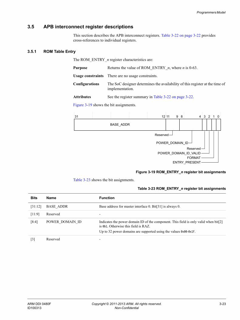
Programmers Model
3.5 APB interconnect register descriptionsThis section describes the APB interconnect registers. Table 3-22 on page 3-22 provides cross-references to individual registers.
3.5.1 ROM Table Entry
The ROM_ENTRY_n register characteristics are:
Purpose Returns the value of ROM_ENTRY_n, where n is 0-63.
Usage constraints There are no usage constraints.
Configurations The SoC designer determines the availability of this register at the time of implementation.
Attributes See the register summary in Table 3-22 on page 3-22.
Figure 3-19 shows the bit assignments.
Figure 3-19 ROM_ENTRY_n register bit assignments
Table 3-23 shows the bit assignments.
31 02
ENTRY_PRESENT
1
FORMAT
12 11
BASE_ADDR
38 49
ReservedPOWER_DOMAIN_ID_VALID
POWER_DOMAIN_ID
Reserved
Table 3-23 ROM_ENTRY_n register bit assignments
Bits Name Function
[31:12] BASE_ADDR Base address for master interface 0. Bit[31] is always 0.
[11:9] Reserved -
[8:4] POWER_DOMAIN_ID Indicates the power domain ID of the component. This field is only valid when bit[2] is 0b1. Otherwise this field is RAZ.Up to 32 power domains are supported using the values 0x00-0x1F.
[3] Reserved -
ARM DDI 0480F Copyright © 2011-2013 ARM. All rights reserved. 3-23ID100313 Non-Confidential

Programmers Model
3.5.2 Peripheral ID4 Register
The PIDR4 characteristics are:
Purpose Part of the set of peripheral identification registers. Contains part of the designer identity and the memory size.
Usage constraints There are no usage constraints.
Configurations This register is available in all configurations.
Attributes See the register summary in Table 3-22 on page 3-22.
Figure 3-20 shows the bit assignments.
Figure 3-20 PIDR4 bit assignments
Table 3-24 shows the bit assignments.
3.5.3 Peripheral ID0 Register
The PIDR0 characteristics are:
Purpose Part of the set of peripheral identification registers. Contains part of the designer-specific part number.
Usage constraints There are no usage constraints.
[2] POWER_DOMAIN_ID_VALID Indicates whether there is a power domain ID specified in the ROM Table entry.0 Indicates that the POWER_DOMAIN_ID field of this register is not
valid.1 Indicates that the POWER_DOMAIN_ID field of this register is valid.
[1] FORMAT Indicates the ROM table entry format, for example, 32-bit or other formats.1 ROM table entry is of 32-bit format.
[0] ENTRY_PRESENT Indicates whether there is a valid ROM entry at this location. 0 Valid ROM table entry not present at this address location.1 Valid ROM table entry present at this address location.
Table 3-23 ROM_ENTRY_n register bit assignments (continued)
Bits Name Function
31 0
Reserved
7
SIZE
8 4
DES_2
3
Table 3-24 PIDR4 bit assignments
Bits Name Function
[31:8] Reserved -
[7:4] SIZE Always 0b0000. Indicates that the device only occupies 4KB of memory.
[3:0] DES_2 Together, PIDR1.DES_0, PIDR2.DES_1, and PIDR4.DES_2 identify the designer of the component.Either targetid[11:8] from the DAP or a sub system specific value.
ARM DDI 0480F Copyright © 2011-2013 ARM. All rights reserved. 3-24ID100313 Non-Confidential

Programmers Model
Configurations This register is available in all configurations.
Attributes See the register summary in Table 3-22 on page 3-22.
Figure 3-21 shows the bit assignments.
Figure 3-21 PIDR0 bit assignments
Table 3-25 shows the bit assignments.
3.5.4 Peripheral ID1 Register
The PIDR1 characteristics are:
Purpose Part of the set of peripheral identification registers. Contains part of the designer-specific part number and part of the designer identity.
Usage constraints There are no usage constraints.
Configurations This register is available in all configurations.
Attributes See the register summary in Table 3-22 on page 3-22.
Figure 3-22 shows the bit assignments.
Figure 3-22 PIDR1 bit assignments
31 0
Reserved
78
PART_0
Table 3-25 PIDR0 bit assignments
Bits Name Function
[31:8] Reserved -
[7:0] PART_0 Bits[7:0] of the 12-bit part number of the component. The designer of the component assigns this part number.Either targetid[23:16] from the DAP or a sub-system identifier.
31 0
Reserved
78
PART_1
4 3
DES_0
ARM DDI 0480F Copyright © 2011-2013 ARM. All rights reserved. 3-25ID100313 Non-Confidential

Programmers Model
Table 3-26 shows the bit assignments.
3.5.5 Peripheral ID2 Register
The PIDR2 characteristics are:
Purpose Part of the set of peripheral identification registers. Contains part of the designer identity and the product revision.
Usage constraints There are no usage constraints.
Configurations This register is available in all configurations.
Attributes See the register summary in Table 3-22 on page 3-22.
Figure 3-23 shows the bit assignments.
Figure 3-23 PIDR2 bit assignments
Table 3-27 shows the bit assignments.
Table 3-26 PIDR1 bit assignments
Bits Name Function
[31:8] Reserved -
[7:4] DES_0 Together, PIDR1.DES_0, PIDR2.DES_1, and PIDR4.DES_2 identify the designer of the component.Either the targetid[4:1] from the DAP or a sub-system identifier.
[3:0] PART_1 Bits[11:8] of the 12-bit part number of the component. The designer of the component assigns this part number.Either the targetid[27:24] from the DAP or a sub-system identifier.
31 0
Reserved
7
REVISION
8 4
DES_1
3 2
JEDEC
Table 3-27 PIDR2 bit assignments
Bits Name Function
[31:8] Reserved -
[7:4] REVISION This reflects either the targetid[31:28] from the DAP or a sub-system identifier.
[3] JEDEC Always 1. Indicates that the JEDEC-assigned designer ID is used.
[2:0] DES_1 Together, PIDR1.DES_0, PIDR2.DES_1, and PIDR4.DES_2 identify the designer of the component.Either the targetid[7:5] from the DAP, or a sub-system identifier.
ARM DDI 0480F Copyright © 2011-2013 ARM. All rights reserved. 3-26ID100313 Non-Confidential

Programmers Model
3.5.6 Peripheral ID3 Register
The PIDR3 characteristics are:
Purpose Part of the set of peripheral identification registers. Contains the REVAND and CMOD fields.
Usage constraints There are no usage constraints.
Configurations This register is available in all configurations.
Attributes See the register summary in Table 3-22 on page 3-22.
Figure 3-24 shows the bit assignments.
Figure 3-24 PIDR3 bit assignments
Table 3-28 shows the bit assignments.
3.5.7 Component ID0 Register
The CIDR0 characteristics are:
Purpose A component identification register that indicates the presence of identification registers.
Usage constraints There are no usage constraints.
Configurations This register is available in all configurations.
Attributes See the register summary in Table 3-22 on page 3-22.
Figure 3-25 shows the bit assignments.
Figure 3-25 CIDR0 bit assignments
31 0
Reserved
7
REVAND
8 4
CMOD
3
Table 3-28 PIDR3 bit assignments
Bits Name Function
[31:8] Reserved -
[7:4] REVAND 0b0000 Indicates that there are no errata fixes to this component.
[3:0] CMOD Customer Modified. Indicates whether the customer has modified the behavior of the component. In most cases, this field is 0b0000. Customers change this value when they make authorized modifications to this component.0b0000 Indicates that the customer has not modified this component.
PRMBL_0
31 8 7 0
Reserved
ARM DDI 0480F Copyright © 2011-2013 ARM. All rights reserved. 3-27ID100313 Non-Confidential

Programmers Model
Table 3-29 shows the bit assignments.
3.5.8 Component ID1 Register
The CIDR1 characteristics are:
Purpose A component identification register that indicates the presence of identification registers. This register also indicates the component class.
Usage constraints There are no usage constraints.
Configurations This register is available in all configurations.
Attributes See the register summary in Table 3-22 on page 3-22.
Figure 3-26 shows the bit assignments.
Figure 3-26 CIDR1 bit assignments
Table 3-30 shows the bit assignments.
3.5.9 Component ID2 Register
The CIDR2 characteristics are:
Purpose A component identification register that indicates the presence of identification registers.
Usage constraints There are no usage constraints.
Configurations This register is available in all configurations.
Attributes See the register summary in Table 3-22 on page 3-22.
Table 3-29 CIDR0 bit assignments
Bits Name Function
[31:8] Reserved -
[7:0] PRMBL_0 Preamble[0]. Contains bits[7:0] of the component identification code.0x0D Bits[7:0] of the identification code.
31 8 7 4 3 0
PRMBL_1CLASSReserved
Table 3-30 CIDR1 bit assignments
Bits Name Function
[31:8] Reserved -
[7:4] CLASS Class of the component, for example, whether the component is a ROM table or a generic CoreSight SoC-400 component. Contains bits[15:12] of the component identification code.0b0001 Indicates that the component is a ROM table.
[3:0] PRMBL_1 Preamble[1]. Contains bits[11:8] of the component identification code.0b0000 Bits[11:8] of the identification code.
ARM DDI 0480F Copyright © 2011-2013 ARM. All rights reserved. 3-28ID100313 Non-Confidential

Programmers Model
Figure 3-27 shows the bit assignments.
Figure 3-27 CIDR2 bit assignments
Table 3-31 shows the bit assignments.
3.5.10 Component ID3 Register
The CIDR3 characteristics are:
Purpose A component identification register that indicates the presence of identification registers.
Usage constraints There are no usage constraints.
Configurations This register is available in all configurations.
Attributes See the register summary in Table 3-22 on page 3-22.
Figure 3-28 shows the bit assignments.
Figure 3-28 CIDR3 bit assignments
Table 3-32 shows the bit assignments.
PRMBL_2
31 8 7 0
Reserved
Table 3-31 CIDR2 bit assignments
Bits Name Function
[31:8] Reserved -
[7:0] PRMBL_2 Preamble[2]. Contains bits[23:16] of the component identification code.0x05 Bits[23:16] of the identification code.
31 0
Reserved
78
PRMBL_3
Table 3-32 CIDR3 bit assignments
Bits Name Function
[31:8] Reserved -
[7:0] PRMBL_3 Preamble[3]. Contains bits[31:24] of the component identification code.0xB1 Bits[31:24] of the identification code.
ARM DDI 0480F Copyright © 2011-2013 ARM. All rights reserved. 3-29ID100313 Non-Confidential

Programmers Model
3.6 ATB funnel register summaryTable 3-33 shows the ATB funnel registers in offset order from the base memory address.
Table 3-33 ATB funnel register summary
Offset Name Type Reset Description
0x000 Ctrl_Reg RW 0x00000300 Funnel Control register on page 3-31
0x004 Priority_Ctrl_Reg RW 0x00000000 Priority Control Register on page 3-33
0xEEC ITATBDATA0 RW 0x00000000 Integration Test ATB Data0 register on page 3-34
0xEF0 ITATBCTR2 RW 0x00000000 Integration Test ATB Control 2 Register on page 3-37
0xEF4 ITATBCTR1 RW 0x00000000 Integration Test ATB Control 1 Register on page 3-38
0xEF8 ITATBCTR0 RW 0x00000000 Integration Test ATB Control 0 Register on page 3-39
0xF00 ITCTRL RW 0x00000000 Integration Mode Control register on page 3-39
0xFA0 CLAIMSET RW 0x0000000F Claim Tag Set register on page 3-40
0xFA4 CLAIMCLR RW 0x00000000 Claim Tag Clear register on page 3-41
0xFB0 LOCKACCESS WO 0x00000000 Lock Access Register on page 3-42
0xFB4 LOCKSTATUS RO 0x00000003 Lock Status Register on page 3-42
0xFB8 AUTHSTATUS RO 0x00000000 Authentication Status register on page 3-43
0xFC8 DEVID RO 0x00000038 Device Configuration register on page 3-44
0xFCC DEVTYPE RO 0x00000012 Device Type Identifier register on page 3-45
0xFD0 PIDR4 RO 0x00000004 Peripheral ID4 Register on page 3-45
0xFD4 - - - Reserved
0xFD8 - - - Reserved
0xFDC - - - Reserved
0xFE0 PIDR0 RO 0x00000008 Peripheral ID0 Register on page 3-46
0xFE4 PIDR1 RO 0x000000B9 Peripheral ID1 Register on page 3-46
0xFE8 PIDR2 RO 0x0000002B Peripheral ID2 Register on page 3-47
0xFEC PIDR3 RO 0x00000000 Peripheral ID3 Register on page 3-48
0xFF0 CIDR0 RO 0x0000000D Component ID0 Register on page 3-48
0xFF4 CIDR1 RO 0x00000090 Component ID1 Register on page 3-49
0xFF8 CIDR2 RO 0x00000005 Component ID2 Register on page 3-50
0xFFC CIDR3 RO 0x000000B1 Component ID3 Register on page 3-50
ARM DDI 0480F Copyright © 2011-2013 ARM. All rights reserved. 3-30ID100313 Non-Confidential

Programmers Model
3.7 ATB funnel register descriptionsThis section describes the ATB funnel registers. Table 3-33 on page 3-30 provides cross-references to individual registers.
The registers are only present when the APB programming interface is chosen.
3.7.1 Funnel Control register
The Ctrl_Reg characteristics are:
Purpose The Ctrl_Reg enables the slave ports and defines the hold time of the slave ports. Hold time refers to the number of transactions that are output on the funnel master port from the same slave when that slave port atvalidsx is HIGH. Hold time does not mention clock cycles in this context.
Usage constraints There are no usage constraints.
Configurations This register is available in all configurations.The number of bits in this register depends on the number of slaves selected in the configuration.
Attributes See the register summary in Table 3-33 on page 3-30.
Figure 3-29 shows the bit assignments.
Figure 3-29 Ctrl_Reg bit assignments
31 12 11 8 7 6 5 4 3 2 1 0
EnS2EnS1EnS0
EnS3EnS4
EnS7EnS6EnS5
HTReserved
ARM DDI 0480F Copyright © 2011-2013 ARM. All rights reserved. 3-31ID100313 Non-Confidential
Programmers Model
Table 3-34 shows the bit assignments.
Table 3-34 Ctrl_Reg bit assignments
Bits Name Function
[31:12] Reserved -
[11:8] HT Hold Time. The formatting scheme can become inefficient when fast switching occurs, and you can use this setting to minimize switching. When a source has nothing to transmit, then another source is selected irrespective of the minimum number of transactions. The ATB funnel holds for the minimum hold time and one additional transaction. The actual hold time is the register value plus 1. The maximum value that can be entered is 0b1110 and this equates to 15 transactions. 0b1111 is reserved.0b0000 1 transaction hold time.0b0001 2 transactions hold time.0b0010 3 transactions hold time.0b0011 4 transactions hold time.0b0100 5 transactions hold time.0b0101 6 transactions hold time.0b0110 7 transactions hold time.0b0111 8 transactions hold time.0b1000 9 transactions hold time.0b1001 10 transactions hold time.0b1010 11 transactions hold time.0b1011 12 transactions hold time.0b1100 13 transactions hold time.0b1101 14 transactions hold time.0b1110 15 transactions hold time.
[7] EnS7 Enable slave port 7. The reset value is 0.0 Slave port disabled.
This excludes the port from the priority selection scheme.1 Slave port enabled.
[6] EnS6 Enable slave port 6.The reset value is 0.0 Slave port disabled.
This excludes the port from the priority selection scheme.1 Slave port enabled.
[5] EnS5 Enable slave port 5.The reset value is 0.0 Slave port disabled.
This excludes the port from the priority selection scheme.1 Slave port enabled.
[4] EnS4 Enable slave port 4.The reset value is 0.0 Slave port disabled.
This excludes the port from the priority selection scheme.1 Slave port enabled.
ARM DDI 0480F Copyright © 2011-2013 ARM. All rights reserved. 3-32ID100313 Non-Confidential

Programmers Model
3.7.2 Priority Control Register
The Priority_Ctrl_Reg characteristics are:
Purpose The Priority_Ctrl_Reg defines the order in which inputs are selected. Each 3-bit field is a priority for each particular slave interface. For example: Location 0 Has the priority value for the first slave port.Location 1 Has the priority value for the second slave port.Location 2 Has the priority value for the third slave port.... ...... ...Location 7 Has the priority value for the eighth slave port.The values represent the priority value for each port number. If you want to give the highest priority to a particular slave port, program the corresponding port with the lowest value. Typically, this is likely to be a port that has more important data or that has a small FIFO and is therefore likely to overflow. If you want to give lowest priority to a particular slave port, program the corresponding slave port with the highest value. The arbitration logic selects the slave with the lowest port number when the same priority value is entered for multiple slaves.
Usage constraints Priority values must not be changed while the corresponding slave port is enabled. Before changing the priority level for one or more slave ports, disable those slave ports using the Funnel Control Register.
Configurations This register is available in all configurations.
[3] EnS3 Enable slave port 3.The reset value is 0.0 Slave port disabled.
This excludes the port from the priority selection scheme.1 Slave port enabled.
[2] EnS2 Enable slave port 2.The reset value is 0.0 Slave port disabled.
This excludes the port from the priority selection scheme.1 Slave port enabled.
[1] EnS1 Enable slave port 1.The reset value is 0.0 Slave port disabled.
This excludes the port from the priority selection scheme.1 Slave port enabled.
[0] EnS0 Enable slave port 0.The reset value is 0.0 Slave port disabled.
This excludes the port from the priority selection scheme.1 Slave port enabled.
Table 3-34 Ctrl_Reg bit assignments (continued)
Bits Name Function
ARM DDI 0480F Copyright © 2011-2013 ARM. All rights reserved. 3-33ID100313 Non-Confidential

Programmers Model
The number of bits in this register depends on the number of slaves selected in the configuration.
Attributes See the register summary in Table 3-33 on page 3-30.
Figure 3-30 shows the bit assignments.
Figure 3-30 Priority_Ctrl_Reg bit assignments
Table 3-35 shows the bit assignments.
3.7.3 Integration Test ATB Data0 register
The ITATBDATA0 register characteristics are:
Purpose Performs different functions depending on whether the access is a read or a write:• A read returns the data from atdatasn, where n is the index of the
slave port that is enabled. For information about ports that are enabled, see Funnel Control register on page 3-31. The read data is only valid when atvalidsn is HIGH.
• A write outputs data to the byte boundaries of atdatam.
Usage constraints There are no usage constraints.
Configurations This register is available in all configurations.
31 24 23 21 20 18 17 15 14 12 11 9 8 6 5 3 2 0
PriPort2PriPort1PriPort0
PriPort3PriPort4
PriPort7PriPort6PriPort5
Reserved
Table 3-35 Priority_Ctrl_Reg bit assignments
Bits Name Function
[31:24] Reserved -
[23:21] PriPort7 Priority value of the eighth slave port.
[20:18] PriPort6 Priority value of the seventh slave port.
[17:15] PriPort5 Priority value of the sixth slave port.
[14:12] PriPort4 Priority value of the fifth slave port.
[11:9] PriPort3 Priority value of the fourth slave port.
[8:6] PriPort2 Priority value of the third slave port.
[5:3] PriPort1 Priority value of the second slave port.
[2:0] PriPort0 Priority value of the first slave port.
ARM DDI 0480F Copyright © 2011-2013 ARM. All rights reserved. 3-34ID100313 Non-Confidential

Programmers Model
Attributes See the register summary in Table 3-33 on page 3-30.
Figure 3-31 shows the bit assignments.
Figure 3-31 ITATBDATA0 register bit assignments
Table 3-36 shows the bit assignments.
31 12 10 89 5 46 1 0
Reserved
15 14 13
ATDATA87
237111617
ATDATA0ATDATA7ATDATA15ATDATA23ATDATA31ATDATA39ATDATA47ATDATA55ATDATA63ATDATA71ATDATA79
ATDATA95ATDATA103ATDATA111ATDATA119ATDATA127
Table 3-36 ITATBDATA0 register bit assignments
Bits Name Function
[31:17] Reserved -
[16] ATDATA127 A read access returns the value of atdatas<x>[127] of the enabled port. A write access writes to atdatam[127] of the enabled port.0 atdata[127] of the enabled port is LOW.1 atdata[127] of the enabled port is HIGH.
[15] ATDATA119 A read access returns the value of atdatas<x>[119] of the enabled port. A write access writes to atdatam[119] of the enabled port.0 atdata[119] of the enabled port is LOW.1 atdata[119] of the enabled port is HIGH.
[14] ATDATA111 A read access returns the value of atdatas<x>[111] of the enabled port. A write access writes to atdatam[111] of the enabled port.0 atdata[111] of the enabled port is LOW.1 atdata[111] of the enabled port is HIGH.
[13] ATDATA103 A read access returns the value of atdatas<x>[103] of the enabled port. A write access writes to atdatam[103] of the enabled port.0 atdata[103] of the enabled port is LOW.1 atdata[103] of the enabled port is HIGH.
ARM DDI 0480F Copyright © 2011-2013 ARM. All rights reserved. 3-35ID100313 Non-Confidential
Programmers Model
[12] ATDATA95 A read access returns the value of atdatas<x>[95] of the enabled port. A write access writes to atdatam[95] of the enabled port.0 atdata[95] of the enabled port is LOW.1 atdata[95] of the enabled port is HIGH.
[11] ATDATA87 A read access returns the value of atdatas<x>[87] of the enabled port. A write access writes to atdatam[87] of the enabled port.0 atdata[87] of the enabled port is LOW.1 atdata[87] of the enabled port is HIGH.
[10] ATDATA79 A read access returns the value of atdatas<x>[79] of the enabled port. A write access writes to atdatam[79] of the enabled port.0 atdata[79] of the enabled port is LOW.1 atdata[79] of the enabled port is HIGH.
[9] ATDATA71 A read access returns the value of atdatas<x>[71] of the enabled port. A write access writes to atdatam[71] of the enabled port.0 atdata[71] of the enabled port is LOW.1 atdata[71] of the enabled port is HIGH.
[8] ATDATA63 A read access returns the value of atdatas<x>[63] of the enabled port. A write access writes to atdatam[63] of the enabled port.0 atdata[63] of the enabled port is LOW.1 atdata[63] of the enabled port is HIGH.
[7] ATDATA55 A read access returns the value of atdatas<x>[55] of the enabled port. A write access writes to atdatam[55] of the enabled port.0 atdata[55] of the enabled port is LOW.1 atdata[55] of the enabled port is HIGH.
[6] ATDATA47 A read access returns the value of atdatas<x>[47] of the enabled port. A write access writes to atdatam[47] of the enabled port.0 atdata[47] of the enabled port is LOW.1 atdata[47] of the enabled port is HIGH.
[5] ATDATA39 A read access returns the value of atdatas<x>[39] of the enabled port. A write access writes to atdatam[39] of the enabled port.0 atdata[39] of the enabled port is LOW.1 atdata[39] of the enabled port is HIGH.
[4] ATDATA31 A read access returns the value of atdatas<x>[31] of the enabled port. A write access writes to atdatam[31] of the enabled port.0 atdata[31] of the enabled port is LOW.1 atdata[31] of the enabled port is HIGH.
[3] ATDATA23 A read access returns the value of atdatas<x>[23] of the enabled port. A write access writes to atdatam[23] of the enabled port.0 atdata[23] of the enabled port is LOW.1 atdata[23] of the enabled port is HIGH.
Table 3-36 ITATBDATA0 register bit assignments (continued)
Bits Name Function
ARM DDI 0480F Copyright © 2011-2013 ARM. All rights reserved. 3-36ID100313 Non-Confidential
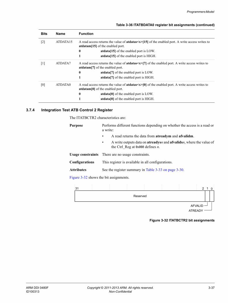
Programmers Model
3.7.4 Integration Test ATB Control 2 Register
The ITATBCTR2 characteristics are:
Purpose Performs different functions depending on whether the access is a read or a write:• A read returns the data from atreadym and afvalidm.• A write outputs data on atreadysn and afvalidsn, where the value of
the Ctrl_Reg at 0x000 defines n.
Usage constraints There are no usage constraints.
Configurations This register is available in all configurations.
Attributes See the register summary in Table 3-33 on page 3-30.
Figure 3-32 shows the bit assignments.
Figure 3-32 ITATBCTR2 bit assignments
[2] ATDATA15 A read access returns the value of atdatas<x>[15] of the enabled port. A write access writes to atdatam[15] of the enabled port.0 atdata[15] of the enabled port is LOW.1 atdata[15] of the enabled port is HIGH.
[1] ATDATA7 A read access returns the value of atdatas<x>[7] of the enabled port. A write access writes to atdatam[7] of the enabled port.0 atdata[7] of the enabled port is LOW.1 atdata[7] of the enabled port is HIGH.
[0] ATDATA0 A read access returns the value of atdatas<x>[0] of the enabled port. A write access writes to atdatam[0] of the enabled port.0 atdata[0] of the enabled port is LOW.1 atdata[0] of the enabled port is HIGH.
Table 3-36 ITATBDATA0 register bit assignments (continued)
Bits Name Function
31 0
Reserved
AFVALID
2 1
ATREADY
ARM DDI 0480F Copyright © 2011-2013 ARM. All rights reserved. 3-37ID100313 Non-Confidential

Programmers Model
Table 3-37 shows the bit assignments.
3.7.5 Integration Test ATB Control 1 Register
The ITATBCTR1 characteristics are:
Purpose Performs different functions depending on whether the access is a read or a write: • A read returns the value of the atidsn signals, where the value of the
Control Register at 0x000 defines n.• A write operation in the register outputs the value written in the
register to atidm. The read data is only valid when atvalidsn is HIGH.
Usage constraints There are no usage constraints.
Configurations This register is available in all configurations.
Attributes See the register summary in Table 3-33 on page 3-30.
Figure 3-33 shows the bit assignments.
Figure 3-33 ITATBCTR1 bit assignments
Table 3-38 shows the bit assignments.
Table 3-37 ITATBCTR2 bit assignments
Bits Name Function
[31:2] Reserved -
[1] AFVALID A read access returns the value of afvalidm.A write access outputs the data to afvalidsn, where the value of the Ctrl_Reg at 0x000 defines n.0 Pin is at logic 0.1 Pin is at logic 1.
[0] ATREADY A read access returns the value of atreadym.A write access outputs the data to atreadysn, where the value of the Ctrl_Reg at 0x000 defines n.0 Pin is at logic 0.1 Pin is at logic 1.
31 0
Reserved
7 6
ATID
Table 3-38 ITATBCTR1 bit assignments
Bits Name Function
[31:7] Reserved -
[6:0] ATID A read returns the value of the atidsn signals, where the value of the Control Register at 0x000 defines n.A write outputs the value to the atidm port.
ARM DDI 0480F Copyright © 2011-2013 ARM. All rights reserved. 3-38ID100313 Non-Confidential

Programmers Model
3.7.6 Integration Test ATB Control 0 Register
The ITATBCTR0 characteristics are:
Purpose Performs different functions depending on whether the access is a read or a write: • A read returns the value of the atvalidsn, atbytessn, and afreadysn
signals, where the value of the Control Register at 0x000 defines n.• A write sets the value of the atvalidm, atbytesm, and afreadym
signals.
Usage constraints There are no usage constraints.
Configurations This register is available in all configurations.
Attributes See the register summary in Table 3-33 on page 3-30.
Figure 3-34 shows the bit assignments.
Figure 3-34 ITATBCTR0 bit assignments
Table 3-39 shows the bit assignments.
3.7.7 Integration Mode Control register
The ITCTRL register characteristics are:
Purpose Enables topology detection. See the ARM® CoreSight™ Architecture Specification.
31 0
Reserved
7 2
Reserved
10 9 8 1
ATVALIDAFREADYATBYTES
Table 3-39 ITATBCTR0 bit assignments
Bits Name Function
[31:10] Reserved -
[9:8] ATBYTES A read returns the value of the atbytessn signal, where the value of the Ctrl_Reg at 0x000 defines n.A write outputs the value to atbytesm.
[7:2] Reserved -
[1] AFREADY A read returns the value of the afreadysn signal, where the value of the Ctrl_Reg at 0x000 defines n.A write outputs the value to afreadym.
[0] ATVALID A read returns the value of the atvalidsn signal, where the value of the Ctrl_Reg at 0x000 defines n.A write outputs the value to atvalidm.
ARM DDI 0480F Copyright © 2011-2013 ARM. All rights reserved. 3-39ID100313 Non-Confidential

Programmers Model
This register enables the component to switch from a functional mode, the default behavior, to integration mode where the inputs and outputs of the component can be directly controlled for the purposes of integration testing and topology detection.
Note When a device is in integration mode, the intended functionality might not
be available.
After performing integration or topology detection, reset the system to ensure correct behavior of CoreSight and other connected system components that the integration or topology detection can affect.
Usage constraints There are no usage constraints.
Configurations This register is available in all configurations.
Attributes See the register summary in Table 3-33 on page 3-30.
Figure 3-35 shows the bit assignments.
Figure 3-35 ITCTRL register bit assignments
Table 3-40 shows the bit assignments.
3.7.8 Claim Tag Set register
The CLAIMSET register characteristics are:
Purpose Software can use the claim tag to coordinate application and debugger access to trace unit functionality. The claim tags have no effect on the operation of the component. The CLAIMSET register sets bits in the claim tag, and determines the number of claim bits implemented.
Usage constraints There are no usage constraints.
Configurations This register is available in all configurations.
Attributes See the register summary in Table 3-33 on page 3-30.
Figure 3-36 on page 3-41 shows the bit assignments.
31 1 0
Reserved
IME
Table 3-40 ITCTRL register bit assignments
Bits Name Function
[31:1] Reserved -
[0] IME Integration Mode Enable. 0 Disable integration mode.1 Enable integration mode.
ARM DDI 0480F Copyright © 2011-2013 ARM. All rights reserved. 3-40ID100313 Non-Confidential

Programmers Model
Figure 3-36 CLAIMSET register bit assignments
Table 3-41 shows the bit assignments.
3.7.9 Claim Tag Clear register
The CLAIMCLR register characteristics are:
Purpose Software can use the claim tag to coordinate application and debugger access to trace unit functionality. The claim tags have no effect on the operation of the component. The CLAIMCLR register sets the bits in the claim tag to 0 and determines the current value of the claim tag.
Usage constraints There are no usage constraints.
Configurations This register is available in all configurations.
Attributes See the register summary in Table 3-33 on page 3-30.
Figure 3-37 shows the bit assignments.
Figure 3-37 CLAIMCLR register bit assignments
Table 3-42 shows the bit assignments.
Reserved
31 4 3 0
SET
Table 3-41 CLAIMSET register bit assignments
Bits Name Function
[31:4] Reserved -
[3:0] SET On reads, for each bit: 1 Claim tag bit is implementedOn writes, for each bit:0 Has no effect.1 Sets the relevant bit of the claim tag.
Reserved
31 4 3 0
CLR
Table 3-42 CLAIMCLR register bit assignments
Bits Name Function
[31:4] Reserved -
[3:0] CLR On reads, for each bit: 0 Claim tag bit is not set.1 Claim tag bit is set.On writes, for each bit: 0 Has no effect.1 Clears the relevant bit of the claim tag.
ARM DDI 0480F Copyright © 2011-2013 ARM. All rights reserved. 3-41ID100313 Non-Confidential

Programmers Model
3.7.10 Lock Access Register
The LAR characteristics are:
Purpose Controls write access from self-hosted, on-chip accesses. The LAR does not affect the accesses using the external debugger interface.
Usage constraints There are no usage constraints.
Configurations This register is available in all configurations.
Attributes See the register summary in Table 3-33 on page 3-30.
Figure 3-38 shows the bit assignments.
Figure 3-38 LAR bit assignments
Table 3-43 shows the bit assignments.
3.7.11 Lock Status Register
The LSR characteristics are:
Purpose Indicates the status of the lock control mechanism. This lock prevents accidental writes. When locked, write accesses are denied for all registers except for the LAR. The lock registers do not affect accesses from the external debug interface. This register reads as 0 when accessed from the external debug interface.
Usage constraints There are no usage constraints.
Configurations This register is available in all configurations.
Attributes See the register summary in Table 3-33 on page 3-30.
Figure 3-39 shows the bit assignments.
Figure 3-39 LSR bit assignments
31 0
KEY
Table 3-43 LAR bit assignments
Bits Name Function
[31:0] KEY Software lock key value. 0xC5ACCE55 Clear the software lock.All other write values set the software lock.
Reserved
31 03 12
SLISLKnTT
ARM DDI 0480F Copyright © 2011-2013 ARM. All rights reserved. 3-42ID100313 Non-Confidential

Programmers Model
Table 3-44 shows the bit assignments.
3.7.12 Authentication Status register
The AUTHSTATUS register characteristics are:
Purpose Reports the required security level and present status.
Usage constraints There are no usage constraints.
Configurations This register is available in all configurations.
Attributes See the register summary in Table 3-33 on page 3-30.
Figure 3-40 shows the bit assignments.
Figure 3-40 AUTHSTATUS register bit assignments
Table 3-45 shows the bit assignments.
Table 3-44 LSR bit assignments
Bits Name Function
[31:3] Reserved -
[2] nTT Register size indicator. Always 0. Indicates that the LAR is implemented as 32-bit.
[1] SLK Software Lock Status. Returns the present lock status of the device, from the current interface.0 Indicates that write operations are permitted from this interface.1 Indicates that write operations are not permitted from this interface. Read
operations are permitted.
[0] SLI Software Lock Implemented. Indicates that a lock control mechanism is present from this interface.0 Indicates that a lock control mechanism is not present from this interface. Write
operations to the LAR are ignored.1 Indicates that a lock control mechanism is present from this interface.
31 8 7 6 5 4 3 2 0
Reserved
NSIDNSNIDSIDSNID
1
Table 3-45 AUTHSTATUS register bit assignments
Bits Name Function
[31:8] Reserved -
[7:6] SNID Indicates the security level for secure non-invasive debug:0b00 Functionality is not implemented or is controlled elsewhere.
ARM DDI 0480F Copyright © 2011-2013 ARM. All rights reserved. 3-43ID100313 Non-Confidential

Programmers Model
3.7.13 Device Configuration register
The DEVID register characteristics are:
Purpose Indicates the capabilities of the component.
Usage constraints There are no usage constraints.
Configurations This register is available in all configurations.
Attributes See the register summary in Table 3-33 on page 3-30.
Figure 3-41 shows the bit assignments.
Figure 3-41 DEVID register bit assignments
Table 3-46 shows the bit assignments.
[5:4] SID Indicates the security level for secure invasive debug:0b00 Functionality is not implemented or is controlled elsewhere.
[3:2] NSNID Indicates the security level for non-secure non-invasive debug:0b00 Functionality is not implemented or is controlled elsewhere.
[1:0] NSID Indicates the security level for non-secure invasive debug:0b00 Functionality is not implemented or is controlled elsewhere.
Table 3-45 AUTHSTATUS register bit assignments (continued)
Bits Name Function
31 0
Reserved
7
SCHEME
8 4
PORTCOUNT
3
Table 3-46 DEVID register bit assignments
Bits Name Function
[31:8] Reserved -
[7:4] SCHEME Indicates the priority scheme implemented in this component.0b0011 Program the slave ports to have higher or lower priority with respect to each other.
[3:0] PORTCOUNT Indicates the number of input ports connected. 0x0 and 0x1 are illegal values.0b0010 Two ATB slave ports.0b0011 Three ATB slave ports.0b0100 Four ATB slave ports.0b0101 Five ATB slave ports.0b0110 Six ATB slave ports.0b0111 Seven ATB slave ports.0b1000 Eight ATB slave ports.
ARM DDI 0480F Copyright © 2011-2013 ARM. All rights reserved. 3-44ID100313 Non-Confidential

Programmers Model
3.7.14 Device Type Identifier register
The DEVTYPE register characteristics are:
Purpose Provides a debugger with information about the component when the Part Number field is not recognized. The debugger can then report this information.
Usage constraints There are no usage constraints.
Configurations This register is available in all configurations.
Attributes See the register summary in Table 3-33 on page 3-30.
Figure 3-42 shows the bit assignments.
Figure 3-42 DEVTYPE register bit assignments
Table 3-47 shows the bit assignments.
3.7.15 Peripheral ID4 Register
The PIDR4 characteristics are:
Purpose Part of the set of peripheral identification registers. Contains part of the designer identity and the memory size.
Usage constraints There are no usage constraints.
Configurations This register is available in all configurations.
Attributes See the register summary in Table 3-33 on page 3-30.
Figure 3-43 shows the bit assignments.
Figure 3-43 PIDR4 bit assignments
31 0
Reserved
7
SUB
8 4
MAJOR
3
Table 3-47 DEVTYPE register bit assignments
Bits Name Function
[31:8] Reserved -
[7:4] SUB Sub-classification of the type of the debug component as specified in the ARM® CoreSight™ Architecture Specification within the major classification as specified in the MAJOR field:0b0001 This component arbitrates ATB inputs mapping to ATB outputs.
[3:0] MAJOR Major classification of the type of the debug component as specified in the ARM® CoreSight™ Architecture Specification for this debug and trace component:0b0010 This component has both ATB inputs and ATB outputs.
31 0
Reserved
7
SIZE
8 4
DES_2
3
ARM DDI 0480F Copyright © 2011-2013 ARM. All rights reserved. 3-45ID100313 Non-Confidential

Programmers Model
Table 3-48 shows the bit assignments.
3.7.16 Peripheral ID0 Register
The PIDR0 characteristics are:
Purpose Part of the set of peripheral identification registers. Contains part of the designer-specific part number.
Usage constraints There are no usage constraints.
Configurations This register is available in all configurations.
Attributes See the register summary in Table 3-33 on page 3-30.
Figure 3-44 shows the bit assignments.
Figure 3-44 PIDR0 bit assignments
Table 3-49 shows the bit assignments.
3.7.17 Peripheral ID1 Register
The PIDR1 characteristics are:
Purpose Part of the set of peripheral identification registers. Contains part of the designer-specific part number and part of the designer identity.
Usage constraints There are no usage constraints.
Configurations This register is available in all configurations.
Attributes See the register summary in Table 3-33 on page 3-30.
Table 3-48 PIDR4 bit assignments
Bits Name Function
[31:8] Reserved -
[7:4] SIZE Always 0b0000. Indicates that the device only occupies 4KB of memory.
[3:0] DES_2 Together, PIDR1.DES_0, PIDR2.DES_1, and PIDR4.DES_2 identify the designer of the component.0b0100 JEDEC continuation code.
31 0
Reserved
78
PART_0
Table 3-49 PIDR0 bit assignments
Bits Name Function
[31:8] Reserved -
[7:0] PART_0 Bits[7:0] of the 12-bit part number of the component. The designer of the component assigns this part number.0x08 Indicates bits[7:0] of the part number of the component.
ARM DDI 0480F Copyright © 2011-2013 ARM. All rights reserved. 3-46ID100313 Non-Confidential
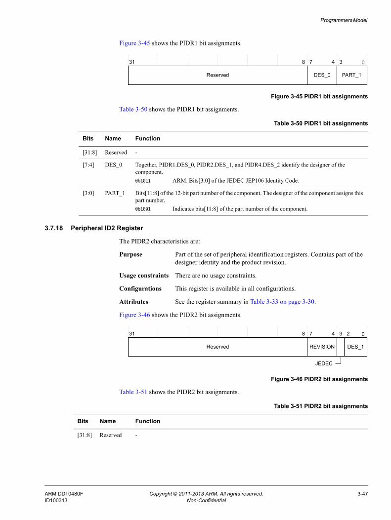
Programmers Model
Figure 3-45 shows the PIDR1 bit assignments.
Figure 3-45 PIDR1 bit assignments
Table 3-50 shows the PIDR1 bit assignments.
3.7.18 Peripheral ID2 Register
The PIDR2 characteristics are:
Purpose Part of the set of peripheral identification registers. Contains part of the designer identity and the product revision.
Usage constraints There are no usage constraints.
Configurations This register is available in all configurations.
Attributes See the register summary in Table 3-33 on page 3-30.
Figure 3-46 shows the PIDR2 bit assignments.
Figure 3-46 PIDR2 bit assignments
Table 3-51 shows the PIDR2 bit assignments.
31 0
Reserved
78
PART_1
4 3
DES_0
Table 3-50 PIDR1 bit assignments
Bits Name Function
[31:8] Reserved -
[7:4] DES_0 Together, PIDR1.DES_0, PIDR2.DES_1, and PIDR4.DES_2 identify the designer of the component.0b1011 ARM. Bits[3:0] of the JEDEC JEP106 Identity Code.
[3:0] PART_1 Bits[11:8] of the 12-bit part number of the component. The designer of the component assigns this part number.0b1001 Indicates bits[11:8] of the part number of the component.
31 0
Reserved
7
REVISION
8 4
DES_1
3 2
JEDEC
Table 3-51 PIDR2 bit assignments
Bits Name Function
[31:8] Reserved -
ARM DDI 0480F Copyright © 2011-2013 ARM. All rights reserved. 3-47ID100313 Non-Confidential

Programmers Model
3.7.19 Peripheral ID3 Register
The PIDR3 characteristics are:
Purpose Part of the set of peripheral identification registers. Contains the REVAND and CMOD fields.
Usage constraints There are no usage constraints.
Configurations This register is available in all configurations.
Attributes See the register summary in Table 3-33 on page 3-30.
Figure 3-47 shows the PIDR3 bit assignments.
Figure 3-47 PIDR3 bit assignments
Table 3-52 shows the PIDR3 bit assignments.
3.7.20 Component ID0 Register
The CIDR0 characteristics are:
Purpose A component identification register that indicates the presence of identification registers.
Usage constraints There are no usage constraints.
Configurations This register is available in all configurations.
Attributes See the register summary in Table 3-33 on page 3-30.
[7:4] REVISION 0b0010 This device is at r1p0.
[3] JEDEC Always 1. Indicates that the JEDEC assigned-designer ID is used.
[2:0] DES_1 Together, PIDR1.DES_0, PIDR2.DES_1, and PIDR4.DES_2 identify the designer of the component.0b011 ARM. Bits[6:4] of the JEDEC JEP106 Identity Code.
Table 3-51 PIDR2 bit assignments (continued)
Bits Name Function
31 0
Reserved
7
REVAND
8 4
CMOD
3
Table 3-52 PIDR3 bit assignments
Bits Name Function
[31:8] Reserved -
[7:4] REVAND 0b0000 Indicates that there are no errata fixes to this component.
[3:0] CMOD Customer Modified. Indicates whether the customer has modified the behavior of the component. In most cases, this field is 0b0000. Customers change this value when they make authorized modifications to this component.0b0000 Indicates that the customer has not modified this component.
ARM DDI 0480F Copyright © 2011-2013 ARM. All rights reserved. 3-48ID100313 Non-Confidential

Programmers Model
Figure 3-48 shows the bit assignments.
Figure 3-48 CIDR0 bit assignments
Table 3-53 shows the bit assignments.
3.7.21 Component ID1 Register
The CIDR1 characteristics are:
Purpose A component identification register that indicates the presence of identification registers. This register also indicates the component class.
Usage constraints There are no usage constraints.
Configurations This register is available in all configurations.
Attributes See the register summary in Table 3-33 on page 3-30.
Figure 3-49 shows the bit assignments.
Figure 3-49 CIDR1 bit assignments
Table 3-54 shows the bit assignments.
PRMBL_0
31 8 7 0
Reserved
Table 3-53 CIDR0 bit assignments
Bits Name Function
[31:8] Reserved -
[7:0] PRMBL_0 Preamble[0]. Contains bits[7:0] of the component identification code.0x0D Bits[7:0] of the identification code.
31 8 7 4 3 0
PRMBL_1CLASSReserved
Table 3-54 CIDR1 bit assignments
Bits Name Function
[31:8] Reserved -
[7:4] CLASS Class of the component, for example, whether the component is a ROM table or a generic CoreSight SoC-400 component. Contains bits[15:12] of the component identification code.0b1001 Indicates that the component is a CoreSight SoC-400 component.
[3:0] PRMBL_1 Preamble[1]. Contains bits[11:8] of the component identification code.0b0000 Bits[11:8] of the identification code.
ARM DDI 0480F Copyright © 2011-2013 ARM. All rights reserved. 3-49ID100313 Non-Confidential

Programmers Model
3.7.22 Component ID2 Register
The CIDR2 characteristics are:
Purpose A component identification register that indicates the presence of identification registers.
Usage constraints There are no usage constraints.
Configurations This register is available in all configurations.
Attributes See the register summary in Table 3-33 on page 3-30.
Figure 3-50 shows the bit assignments.
Figure 3-50 CIDR2 bit assignments
Table 3-55 shows the bit assignments.
3.7.23 Component ID3 Register
The CIDR3 characteristics are:
Purpose A component identification register that indicates the presence of identification registers.
Usage constraints There are no usage constraints.
Configurations This register is available in all configurations.
Attributes See the register summary in Table 3-33 on page 3-30.
Figure 3-51 shows the bit assignments.
Figure 3-51 CIDR3 bit assignments
PRMBL_2
31 8 7 0
Reserved
Table 3-55 CIDR2 bit assignments
Bits Name Function
[31:8] Reserved -
[7:0] PRMBL_2 Preamble[2]. Contains bits[23:16] of the component identification code.0x05 Bits[23:16] of the identification code.
31 0
Reserved
78
PRMBL_3
ARM DDI 0480F Copyright © 2011-2013 ARM. All rights reserved. 3-50ID100313 Non-Confidential

Programmers Model
Table 3-56 shows the bit assignments.
Table 3-56 CIDR3 bit assignments
Bits Name Function
[31:8] Reserved -
[7:0] PRMBL_3 Preamble[3]. Contains bits[31:24] of the component identification code.0xB1 Bits[31:24] of the identification code.
ARM DDI 0480F Copyright © 2011-2013 ARM. All rights reserved. 3-51ID100313 Non-Confidential

Programmers Model
3.8 ATB replicator register summaryTable 3-57 shows the ATB replicator registers in offset order from the base memory address.
Table 3-57 ATB replicator register summary
Offset Name Type Reset Description
0x000 IDFILTER0 RW 0x00000000 ID filtering for ATB master port 0 on page 3-53
0x004 IDFILTER1 RW 0x00000000 ID filtering for ATB master port 1 on page 3-54
0xEFC ITATBCTR0 WO 0x00000000 Integration Mode ATB Control 0 Register on page 3-55
0xEF8 ITATBCTR1 RO 0x00000000 Integration Mode ATB Control 1 Register on page 3-56
0xF00 ITCTRL RW 0x00000000 Integration Mode Control register on page 3-57
0xFA0 CLAIMSET RW 0x0000000F Claim Tag Set register on page 3-58
0xFA4 CLAIMCLR RW 0x00000000 Claim Tag Clear register on page 3-59
0xFB0 LAR WO 0x00000000 Lock Access Register on page 3-59
0xFB4 LSR RO 0x00000003 Lock Status Register on page 3-60
0xFB8 AUTHSTATUS RO 0x00000000 Authentication Status register on page 3-61
0xFC8 DEVID RO 0x00000002 Device Configuration register on page 3-61
0xFCC DEVTYPE RO 0x00000022 Device Type Identifier register on page 3-62
0xFD0 PIDR4 RO 0x00000004 Peripheral ID4 Register on page 3-63
0xFD4 - - - Reserved
0xFD8 - - - Reserved
0xFDC - - - Reserved
0xFE0 PIDR0 RO 0x00000009 Peripheral ID0 Register on page 3-63
0xFE4 PIDR1 RO 0x000000B9 Peripheral ID1 Register on page 3-64
0xFE8 PIDR2 RO 0x0000001B Peripheral ID2 Register on page 3-64
0xFEC PIDR3 RO 0x00000000 Peripheral ID3 Register on page 3-65
0xFF0 CIDR0 RO 0x0000000D Component ID0 Register on page 3-66
0xFF4 CIDR1 RO 0x00000090 Component ID1 Register on page 3-66
0xFF8 CIDR2 RO 0x00000005 Component ID2 Register on page 3-67
0xFFC CIDR3 RO 0x000000B1 Component ID3 Register on page 3-67
ARM DDI 0480F Copyright © 2011-2013 ARM. All rights reserved. 3-52ID100313 Non-Confidential

Programmers Model
3.9 ATB replicator register descriptionsThis section describes the ATB replicator registers. Table 3-57 on page 3-52 provides cross-references to individual registers.
The registers are only present when you select the APB programming interface.
3.9.1 ID filtering for ATB master port 0
The IDFILTER0 register characteristics are:
Purpose Enables the programming of ID filtering for master port 0.
Usage constraints There are no usage constraints.
Configurations This register is available in all configurations.
Attributes See the register summary in Table 3-57 on page 3-52.
Figure 3-52 shows the bit assignments.
Figure 3-52 IDFILTER0 register bit assignments
Table 3-58 shows the bit assignments.
31 8 7 6 5 4 3 2 1 0
ID0_20_2FID0_10_1FID0_0_F
ID0_30_3FID0_40_4F
ID0_70_7FID0_60_6FID0_50_5F
Reserved
Table 3-58 IDFILTER0 register bit assignments
Bits Name Function
[31:8] Reserved -
[7] ID0_70_7F Enable or disable ID filtering for IDs 0x70-0x7F.0 Transactions with these IDs are passed on to ATB master port 0.1 Transactions with these IDs are discarded by the replicator.
[6] ID0_60_6F Enable or disable ID filtering for IDs 0x60-0x6F.0 Transactions with these IDs are passed on to ATB master port 0.1 Transactions with these IDs are discarded by the replicator.
[5] ID0_50_5F Enable or disable ID filtering for IDs 0x50-0x5F.0 Transactions with these IDs are passed on to ATB master port 0.1 Transactions with these IDs are discarded by the replicator.
[4] ID0_40_4F Enable or disable ID filtering for IDs 0x40-0x4F.0 Transactions with these IDs are passed on to ATB master port 0.1 Transactions with these IDs are discarded by the replicator.
ARM DDI 0480F Copyright © 2011-2013 ARM. All rights reserved. 3-53ID100313 Non-Confidential

Programmers Model
3.9.2 ID filtering for ATB master port 1
The IDFILTER1 register characteristics are:
Purpose Enables the programming of ID filtering for master port 1.
Usage constraints There are no usage constraints.
Configurations This register is available in all configurations.
Attributes See the register summary in Table 3-57 on page 3-52.
Figure 3-53 shows the bit assignments.
Figure 3-53 IDFILTER1 register bit assignments
[3] ID0_30_3F Enable or disable ID filtering for IDs 0x30-0x3F.0 Transactions with these IDs are passed on to ATB master port 0.1 Transactions with these IDs are discarded by the replicator.
[2] ID0_20_2F Enable or disable ID filtering for IDs 0x20-0x2F.0 Transactions with these IDs are passed on to ATB master port 0.1 Transactions with these IDs are discarded by the replicator.
[1] ID0_10_1F Enable or disable ID filtering for IDs 0x10-0x1F.0 Transactions with these IDs are passed on to ATB master port 0.1 Transactions with these IDs are discarded by the replicator.
[0] ID0_0_F Enable or disable ID filtering for IDs 0x0-0xF.0 Transactions with these IDs are passed on to ATB master port 0.1 Transactions with these IDs are discarded by the replicator.
Table 3-58 IDFILTER0 register bit assignments (continued)
Bits Name Function
31 8 7 6 5 4 3 2 1 0
ID1_20_2FID1_10_1FID1_0_F
ID1_30_3FID1_40_4F
ID1_70_7FID1_60_6FID1_50_5F
Reserved
ARM DDI 0480F Copyright © 2011-2013 ARM. All rights reserved. 3-54ID100313 Non-Confidential

Programmers Model
Table 3-59 shows the bit assignments.
3.9.3 Integration Mode ATB Control 0 Register
The ITATBCTR0 characteristics are:
Purpose Controls the value of the atvalidm0, atvalidm1, and atreadys outputs in integration mode.
Usage constraints There are no usage constraints.
Configurations This register is available in all configurations.
Attributes See the register summary in Table 3-57 on page 3-52.
Figure 3-54 on page 3-56 shows the bit assignments.
Table 3-59 IDFILTER1 register bit assignments
Bits Name Function
[31:8] Reserved -
[7] ID1_70_7F Enable or disable ID filtering for IDs 0x70-0x7F.0 Transactions with these IDs are passed on to ATB master port 1.1 Transactions with these IDs are discarded by the replicator.
[6] ID1_60_6F Enable or disable ID filtering for IDs 0x60-0x6F.0 Transactions with these IDs are passed on to ATB master port 1.1 Transactions with these IDs are discarded by the replicator.
[5] ID1_50_5F Enable or disable ID filtering for IDs 0x50-0x5F.0 Transactions with these IDs are passed on to ATB master port 1.1 Transactions with these IDs are discarded by the replicator.
[4] ID1_40_4F Enable or disable ID filtering for IDs 0x40-0x4F.0 Transactions with these IDs are passed on to ATB master port 1.1 Transactions with these IDs are discarded by the replicator.
[3] ID1_30_3F Enable or disable ID filtering for IDs 0x30-0x3F.0 Transactions with these IDs are passed on to ATB master port 1.1 Transactions with these IDs are discarded by the replicator.
[2] ID1_20_2F Enable or disable ID filtering for IDs 0x20-0x2F.0 Transactions with these IDs are passed on to ATB master port 1.1 Transactions with these IDs are discarded by the replicator.
[1] ID1_10_1F Enable or disable ID filtering for IDs 0x10-0x1F.0 Transactions with these IDs are passed on to ATB master port 1.1 Transactions with these IDs are discarded by the replicator.
[0] ID1_0_F Enable or disable ID filtering for IDs 0x0-0xF.0 Transactions with these IDs are passed on to ATB master port 1.1 Transactions with these IDs are discarded by the replicator.
ARM DDI 0480F Copyright © 2011-2013 ARM. All rights reserved. 3-55ID100313 Non-Confidential

Programmers Model
Figure 3-54 ITATBCTR0 bit assignments
Table 3-60 shows the bit assignments.
3.9.4 Integration Mode ATB Control 1 Register
The ITATBCTR1 characteristics are:
Purpose Returns the value of the atreadym0, atreadym1, and atvalids inputs in integration mode.
Usage constraints There are no usage constraints.
Configurations This register is available in all configurations.
Attributes See the register summary in Table 3-57 on page 3-52.
Figure 3-55 on page 3-57 shows the bit assignments.
31 0
Reserved
4 2
Reserved
3 1
ATVALIDM0
ATREADYS
5
ATVALIDM1Reserved
Table 3-60 ITATBCTR0 bit assignments
Bits Name Function
[31:5] Reserved -
[4] ATREADYS Sets the value of the atreadys output.0 Drive logic 0 on the atreadys output.1 Drive logic 1 on the atreadys output.
[3] Reserved -
[2] ATVALIDM1 Sets the value of the atvalidm1 output.0 Drive logic 0 on the atvalidm1 output.1 Drive logic 1 on the atvalidm1 output.
[1] Reserved -
[0] ATVALIDM0 Sets the value of the atvalidm0 output.0 Drive logic 0 on the atvalidm0 output.1 Drive logic 1 on the atvalidm0 output.
ARM DDI 0480F Copyright © 2011-2013 ARM. All rights reserved. 3-56ID100313 Non-Confidential
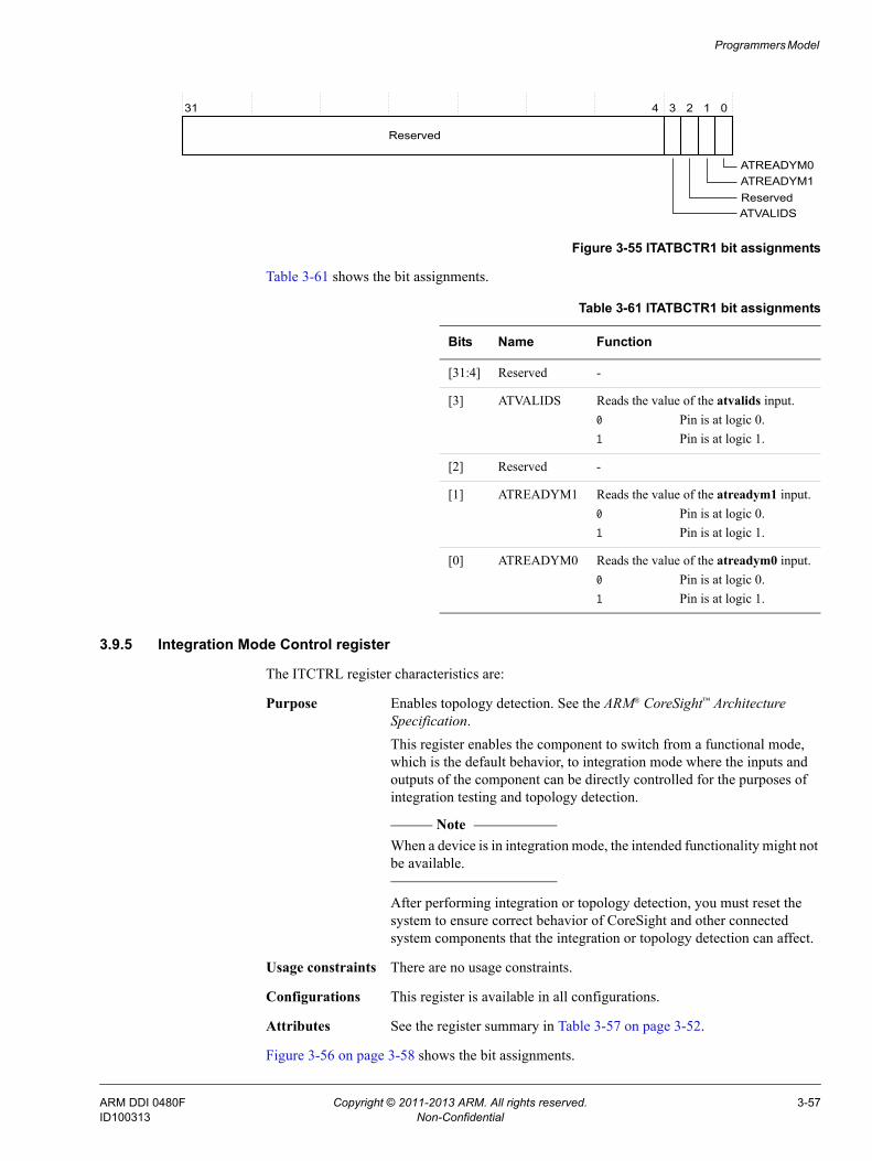
Programmers Model
Figure 3-55 ITATBCTR1 bit assignments
Table 3-61 shows the bit assignments.
3.9.5 Integration Mode Control register
The ITCTRL register characteristics are:
Purpose Enables topology detection. See the ARM® CoreSight™ Architecture Specification.This register enables the component to switch from a functional mode, which is the default behavior, to integration mode where the inputs and outputs of the component can be directly controlled for the purposes of integration testing and topology detection.
Note When a device is in integration mode, the intended functionality might not
be available.
After performing integration or topology detection, you must reset the system to ensure correct behavior of CoreSight and other connected system components that the integration or topology detection can affect.
Usage constraints There are no usage constraints.
Configurations This register is available in all configurations.
Attributes See the register summary in Table 3-57 on page 3-52.
Figure 3-56 on page 3-58 shows the bit assignments.
31 0
Reserved
4 2
ATVALIDS
3 1
ATREADYM0
ReservedATREADYM1
Table 3-61 ITATBCTR1 bit assignments
Bits Name Function
[31:4] Reserved -
[3] ATVALIDS Reads the value of the atvalids input.0 Pin is at logic 0.1 Pin is at logic 1.
[2] Reserved -
[1] ATREADYM1 Reads the value of the atreadym1 input.0 Pin is at logic 0.1 Pin is at logic 1.
[0] ATREADYM0 Reads the value of the atreadym0 input.0 Pin is at logic 0.1 Pin is at logic 1.
ARM DDI 0480F Copyright © 2011-2013 ARM. All rights reserved. 3-57ID100313 Non-Confidential

Programmers Model
Figure 3-56 ITCTRL register bit assignments
Table 3-62 shows the bit assignments.
3.9.6 Claim Tag Set register
The CLAIMSET register characteristics are:
Purpose Software can use the claim tag to coordinate application and debugger access to trace unit functionality. The claim tags have no effect on the operation of the component. The CLAIMSET register sets bits in the claim tag, and determines the number of claim bits implemented.
Usage constraints There are no usage constraints.
Configurations This register is available in all configurations.
Attributes See the register summary in Table 3-57 on page 3-52.
Figure 3-57 shows the bit assignments.
Figure 3-57 CLAIMSET register bit assignments
Table 3-63 shows the bit assignments.
31 0
Reserved
1
IME
Table 3-62 ITCTRL register bit assignments
Bits Name Function
[31:1] Reserved -
[0] IME Integration Mode Enable. 0 Disable integration mode.1 Enable integration mode.
Reserved
31 4 3 0
SET
Table 3-63 CLAIMSET register bit assignments
Bits Name Function
[31:4] Reserved -
[3:0] SET On reads, for each bit: 1 Claim tag bit is implementedOn writes, for each bit:0 Has no effect.1 Sets the relevant bit of the claim tag.
ARM DDI 0480F Copyright © 2011-2013 ARM. All rights reserved. 3-58ID100313 Non-Confidential

Programmers Model
3.9.7 Claim Tag Clear register
The CLAIMCLR register characteristics are:
Purpose Software can use the claim tag to coordinate application and debugger access to trace unit functionality. The claim tags have no effect on the operation of the component. The CLAIMCLR register sets the bits in the claim tag to 0 and determines the current value of the claim tag.
Usage constraints There are no usage constraints.
Configurations This register is available in all configurations.
Attributes See the register summary in Table 3-57 on page 3-52.
Figure 3-58 shows the bit assignments.
Figure 3-58 CLAIMCLR register bit assignments
Table 3-64 shows the bit assignments.
3.9.8 Lock Access Register
The LAR characteristics are:
Purpose Controls write access from self-hosted, on-chip accesses. The LAR does not affect the accesses using the external debugger interface.
Usage constraints There are no usage constraints.
Configurations This register is available in all configurations.
Attributes See the register summary in Table 3-57 on page 3-52.
Figure 3-59 shows the bit assignments.
Figure 3-59 LAR bit assignments
Reserved
31 4 3 0
CLR
Table 3-64 CLAIMCLR register bit assignments
Bits Name Function
[31:4] Reserved -
[3:0] CLR On reads, for each bit: 0 Claim tag bit is not set.1 Claim tag bit is set.On writes, for each bit: 0 Has no effect.1 Clears the relevant bit of the claim tag.
31 0
KEY
ARM DDI 0480F Copyright © 2011-2013 ARM. All rights reserved. 3-59ID100313 Non-Confidential
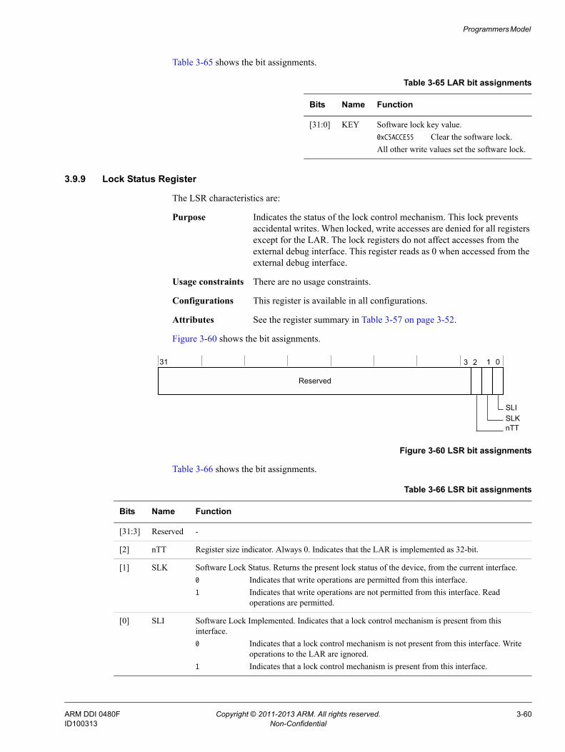
Programmers Model
Table 3-65 shows the bit assignments.
3.9.9 Lock Status Register
The LSR characteristics are:
Purpose Indicates the status of the lock control mechanism. This lock prevents accidental writes. When locked, write accesses are denied for all registers except for the LAR. The lock registers do not affect accesses from the external debug interface. This register reads as 0 when accessed from the external debug interface.
Usage constraints There are no usage constraints.
Configurations This register is available in all configurations.
Attributes See the register summary in Table 3-57 on page 3-52.
Figure 3-60 shows the bit assignments.
Figure 3-60 LSR bit assignments
Table 3-66 shows the bit assignments.
Table 3-65 LAR bit assignments
Bits Name Function
[31:0] KEY Software lock key value. 0xC5ACCE55 Clear the software lock.All other write values set the software lock.
Reserved
31 03 12
SLISLKnTT
Table 3-66 LSR bit assignments
Bits Name Function
[31:3] Reserved -
[2] nTT Register size indicator. Always 0. Indicates that the LAR is implemented as 32-bit.
[1] SLK Software Lock Status. Returns the present lock status of the device, from the current interface.0 Indicates that write operations are permitted from this interface.1 Indicates that write operations are not permitted from this interface. Read
operations are permitted.
[0] SLI Software Lock Implemented. Indicates that a lock control mechanism is present from this interface.0 Indicates that a lock control mechanism is not present from this interface. Write
operations to the LAR are ignored.1 Indicates that a lock control mechanism is present from this interface.
ARM DDI 0480F Copyright © 2011-2013 ARM. All rights reserved. 3-60ID100313 Non-Confidential

Programmers Model
3.9.10 Authentication Status register
The AUTHSTATUS register characteristics are:
Purpose Reports the required security level and present status.
Usage constraints There are no usage constraints.
Configurations This register is available in all configurations.
Attributes See the register summary in Table 3-57 on page 3-52.
Figure 3-61 shows the bit assignments.
Figure 3-61 AUTHSTATUS register bit assignments
Table 3-67 shows the bit assignments.
3.9.11 Device Configuration register
The DEVID register characteristics are:
Purpose Indicates the capabilities of the component.
Usage constraints There are no usage constraints.
Configurations This register is available in all configurations.
Attributes See the register summary in Table 3-57 on page 3-52.
Figure 3-62 on page 3-62 shows the bit assignments.
31 8 7 6 5 4 3 2 0
Reserved
NSIDNSNIDSIDSNID
1
Table 3-67 AUTHSTATUS register bit assignments
Bits Name Function
[31:8] Reserved -
[7:6] SNID Indicates the security level for secure non-invasive debug:0b00 Functionality is not implemented or is controlled elsewhere.
[5:4] SID Indicates the security level for secure invasive debug:0b00 Functionality is not implemented or is controlled elsewhere.
[3:2] NSNID Indicates the security level for non-secure non-invasive debug:0b00 Functionality is not implemented or is controlled elsewhere.
[1:0] NSID Indicates the security level for non-secure invasive debug:0b00 Functionality is not implemented or is controlled elsewhere.
ARM DDI 0480F Copyright © 2011-2013 ARM. All rights reserved. 3-61ID100313 Non-Confidential

Programmers Model
Figure 3-62 DEVID register bit assignments
Table 3-68 shows the bit assignments.
3.9.12 Device Type Identifier register
The DEVTYPE register characteristics are:
Purpose Provides a debugger with information about the component when the Part Number field is not recognized. The debugger can then report this information.
Usage constraints There are no usage constraints.
Configurations This register is available in all configurations.
Attributes See the register summary in Table 3-57 on page 3-52.
Figure 3-63 shows the bit assignments.
Figure 3-63 DEVTYPE register bit assignments
Table 3-69 shows the bit assignments.
31 0
Reserved
4
PORTNUM
3
Table 3-68 DEVID register bit assignments
Bits Name Function
[31:4] Reserved -
[3:0] PORTNUM Indicates the number of master ports implemented.0b0010 Two master ports are implemented.
31 0
Reserved
7
SUB
8 4
MAJOR
3
Table 3-69 DEVTYPE register bit assignments
Bits Name Function
[31:8] Reserved -
[7:4] SUB Sub-classification of the type of the debug component as specified in the ARM® CoreSight™ Architecture Specification within the major classification as specified in the MAJOR field.0b0010 Indicates that this component replicates trace from a single source to multiple
targets.
[3:0] MAJOR Major classification of the type of the debug component as specified in the ARM® CoreSight™ Architecture Specification for this debug and trace component.0b0010 Indicates that this component has ATB inputs and outputs.
ARM DDI 0480F Copyright © 2011-2013 ARM. All rights reserved. 3-62ID100313 Non-Confidential

Programmers Model
3.9.13 Peripheral ID4 Register
The PIDR4 characteristics are:
Purpose Part of the set of peripheral identification registers. Contains part of the designer identity and the memory size.
Usage constraints There are no usage constraints.
Configurations This register is available in all configurations.
Attributes See the register summary in Table 3-57 on page 3-52.
Figure 3-64 shows the bit assignments.
Figure 3-64 PIDR4 bit assignments
Table 3-70 shows the bit assignments.
3.9.14 Peripheral ID0 Register
The PIDR0 characteristics are:
Purpose Part of the set of peripheral identification registers. Contains part of the designer-specific part number.
Usage constraints There are no usage constraints.
Configurations This register is available in all configurations.
Attributes See the register summary in Table 3-57 on page 3-52.
Figure 3-65 shows the bit assignments.
Figure 3-65 PIDR0 bit assignments
31 0
Reserved
7
SIZE
8 4
DES_2
3
Table 3-70 PIDR4 bit assignments
Bits Name Function
[31:8] Reserved -
[7:4] SIZE Always 0b0000. Indicates that the device only occupies 4KB of memory.
[3:0] DES_2 Together, PIDR1.DES_0, PIDR2.DES_1, and PIDR4.DES_2 identify the designer of the component.0b0100 JEDEC continuation code.
31 0
Reserved
78
PART_0
ARM DDI 0480F Copyright © 2011-2013 ARM. All rights reserved. 3-63ID100313 Non-Confidential

Programmers Model
Table 3-71 shows the bit assignments.
3.9.15 Peripheral ID1 Register
The PIDR1 characteristics are:
Purpose Part of the set of peripheral identification registers. Contains part of the designer-specific part number and part of the designer identity.
Usage constraints There are no usage constraints.
Configurations This register is available in all configurations.
Attributes See the register summary in Table 3-57 on page 3-52.
Figure 3-66 shows the bit assignments.
Figure 3-66 PIDR1 bit assignments
Table 3-72 shows the bit assignments.
3.9.16 Peripheral ID2 Register
The PIDR2 characteristics are:
Purpose Part of the set of peripheral identification registers. Contains part of the designer identity and the product revision.
Usage constraints There are no usage constraints.
Configurations This register is available in all configurations.
Table 3-71 PIDR0 bit assignments
Bits Name Function
[31:8] Reserved -
[7:0] PART_0 Bits[7:0] of the 12-bit part number of the component. The designer of the component assigns this part number.0x09 Indicates bits[7:0] of the part number of the component.
31 0
Reserved
78
PART_1
4 3
DES_0
Table 3-72 PIDR1 bit assignments
Bits Name Function
[31:8] Reserved -
[7:4] DES_0 Together, PIDR1.DES_0, PIDR2.DES_1, and PIDR4.DES_2 identify the designer of the component.0b1011 ARM. Bits[3:0] of the JEDEC JEP106 Identity Code.
[3:0] PART_1 Bits[11:8] of the 12-bit part number of the component. The designer of the component assigns this part number.0b1001 Indicates bits[11:8] of the part number of the component.
ARM DDI 0480F Copyright © 2011-2013 ARM. All rights reserved. 3-64ID100313 Non-Confidential

Programmers Model
Attributes See the register summary in Table 3-57 on page 3-52.
Figure 3-67 shows the bit assignments.
Figure 3-67 PIDR2 bit assignments
Table 3-73 shows the bit assignments.
3.9.17 Peripheral ID3 Register
The PIDR3 characteristics are:
Purpose Part of the set of peripheral identification registers. Contains the REVAND and CMOD fields.
Usage constraints There are no usage constraints.
Configurations This register is available in all configurations.
Attributes See the register summary in Table 3-57 on page 3-52.
Figure 3-68 shows the bit assignments.
Figure 3-68 PIDR3 bit assignments
31 0
Reserved
7
REVISION
8 4
DES_1
3 2
JEDEC
Table 3-73 PIDR2 bit assignments
Bits Name Function
[31:8] Reserved -
[7:4] REVISION 0b0001 This device is at r0p0.
[3] JEDEC Always 1. Indicates that the JEDEC-assigned designer ID is used.
[2:0] DES_1 Together, PIDR1.DES_0, PIDR2.DES_1, and PIDR4.DES_2 identify the designer of the component.0b011 ARM. Bits[6:4] of the JEDEC JEP106 Identity Code.
31 0
Reserved
7
REVAND
8 4
CMOD
3
ARM DDI 0480F Copyright © 2011-2013 ARM. All rights reserved. 3-65ID100313 Non-Confidential

Programmers Model
Table 3-74 shows the bit assignments.
3.9.18 Component ID0 Register
The CIDR0 characteristics are:
Purpose A component identification register that indicates the presence of identification registers.
Usage constraints There are no usage constraints.
Configurations This register is available in all configurations.
Attributes See the register summary in Table 3-57 on page 3-52.
Figure 3-69 shows the bit assignments.
Figure 3-69 CIDR0 bit assignments
Table 3-75 shows the bit assignments.
3.9.19 Component ID1 Register
The CIDR1 characteristics are:
Purpose A component identification register that indicates the presence of identification registers. This register also indicates the component class.
Usage constraints There are no usage constraints.
Configurations This register is available in all configurations.
Attributes See the register summary in Table 3-57 on page 3-52.
Figure 3-70 on page 3-67 shows the bit assignments.
Table 3-74 PIDR3 bit assignments
Bits Name Function
[31:8] Reserved -
[7:4] REVAND 0b0000 Indicates that there are no errata fixes to this component.
[3:0] CMOD Customer Modified. Indicates whether the customer has modified the behavior of the component. In most cases, this field is 0b0000. Customers change this value when they make authorized modifications to this component.0b0000 Indicates that the customer has not modified this component.
PRMBL_0
31 8 7 0
Reserved
Table 3-75 CIDR0 bit assignments
Bits Name Function
[31:8] Reserved -
[7:0] PRMBL_0 Preamble[0]. Contains bits[7:0] of the component identification code.0x0D Bits[7:0] of the identification code.
ARM DDI 0480F Copyright © 2011-2013 ARM. All rights reserved. 3-66ID100313 Non-Confidential

Programmers Model
Figure 3-70 CIDR1 bit assignments
Table 3-76 shows the bit assignments.
3.9.20 Component ID2 Register
The CIDR2 characteristics are:
Purpose A component identification register that indicates the presence of identification registers.
Usage constraints There are no usage constraints.
Configurations This register is available in all configurations.
Attributes See the register summary in Table 3-57 on page 3-52.
Figure 3-71 shows the bit assignments.
Figure 3-71 CIDR2 bit assignments
Table 3-77 shows the bit assignments.
3.9.21 Component ID3 Register
The CIDR3 characteristics are:
Purpose A component identification register that indicates the presence of identification registers.
31 8 7 4 3 0
PRMBL_1CLASSReserved
Table 3-76 CIDR1 bit assignments
Bits Name Function
[31:8] Reserved -
[7:4] CLASS Class of the component, for example, whether the component is a ROM table or a generic CoreSight SoC-400 component. Contains bits[15:12] of the component identification code.0b1001 Indicates that the component is a CoreSight SoC-400 component.
[3:0] PRMBL_1 Preamble[1]. Contains bits[11:8] of the component identification code.0b0000 Bits[11:8] of the identification code.
PRMBL_2
31 8 7 0
Reserved
Table 3-77 CIDR2 bit assignments
Bits Name Function
[31:8] Reserved -
[7:0] PRMBL_2 Preamble[2]. Contains bits[23:16] of the component identification code.0x05 Bits[23:16] of the identification code.
ARM DDI 0480F Copyright © 2011-2013 ARM. All rights reserved. 3-67ID100313 Non-Confidential

Programmers Model
Usage constraints There are no usage constraints.
Configurations This register is available in all configurations.
Attributes See the register summary in Table 3-57 on page 3-52.
Figure 3-72 shows the bit assignments.
Figure 3-72 CIDR3 bit assignments
Table 3-78 shows the bit assignments.
31 0
Reserved
78
PRMBL_3
Table 3-78 CIDR3 bit assignments
Bits Name Function
[31:8] Reserved -
[7:0] PRMBL_3 Preamble[3]. Contains bits[31:24] of the component identification code.0xB1 Bits[31:24] of the identification code.
ARM DDI 0480F Copyright © 2011-2013 ARM. All rights reserved. 3-68ID100313 Non-Confidential

Programmers Model
3.10 ETB register summaryTable 3-79 shows the ETB registers in offset order from the base memory address.
Table 3-79 ETB register summary
Offset Name Type Reset Description
0x004 RDP RO 0x00000000 ETB RAM Depth register on page 3-71
0x00C STS RO 0x00000008 ETB Status register on page 3-71
0x010 RRD RO 0x00000000 ETB RAM Read Data register on page 3-72
0x014 RRP RW 0x00000000 ETB RAM Read Pointer register on page 3-73
0x018 RWP RW 0x00000000 ETB RAM Write Pointer register on page 3-74
0x01C TRG RW 0x00000000 ETB Trigger Counter register on page 3-74
0x020 CTL RW 0x00000000 ETB Control register on page 3-75
0x024 RWD WO 0x00000000 ETB RAM Write Data register on page 3-76
0x300 FFSR RO 0x00000002 ETB Formatter and Flush Status Register on page 3-76
0x304 FFCR RW 0x00000000 ETB Formatter and Flush Control Register on page 3-77
0xEE0 ITMISCOP0 WO 0x00000000 Integration Test Miscellaneous Output register 0 on page 3-79
0xEE4 ITTRFLINACK WO 0x00000000 Integration Test Trigger In and Flush In Acknowledge register on page 3-80
0xEE8 ITTRFLIN RO 0x00000000 Integration Test Trigger In and Flush In register on page 3-81
0xEEC ITATBDATA0 RO 0x00000000 Integration Test ATB Data register 0 on page 3-81
0xEF0 ITATBCTR2 WO 0x00000000 Integration Test ATB Control Register 2 on page 3-82
0xEF4 ITATBCTR1 RO 0x00000000 Integration Test ATB Control Register 1 on page 3-83
0xEF8 ITATBCTR0 RO 0x00000000 Integration Test ATB Control Register 0 on page 3-84
0xF00 ITCTRL RW 0x00000000 Integration Mode Control register on page 3-84
0xFA0 CLAIMSET RW 0x0000000F Claim Tag Set register on page 3-85
0xFA4 CLAIMCLR RW 0x00000000 Claim Tag Clear register on page 3-86
0xFB0 LAR WO 0x00000000 Lock Access Register on page 3-86
0xFB4 LSR RO 0x00000003 Lock Status Register on page 3-87
0xFB8 AUTHSTATUS RO 0x00000000 Authentication Status register on page 3-88
0xFC8 DEVID RO 0x00000000 Device Configuration register on page 3-89
0xFCC DEVTYPE RO 0x00000021 Device Type Identifier register on page 3-89
0xFD0 PIDR4 RO 0x00000004 Peripheral ID4 Register on page 3-90
0xFD4 - - - Reserved
0xFD8 - - - Reserved
0xFDC - - - Reserved
0xFE0 PIDR0 RO 0x00000007 Peripheral ID0 Register on page 3-91
ARM DDI 0480F Copyright © 2011-2013 ARM. All rights reserved. 3-69ID100313 Non-Confidential

Programmers Model
0xFE4 PIDR1 RO 0x000000B9 Peripheral ID1 Register on page 3-91
0xFE8 PIDR2 RO 0x0000003B Peripheral ID2 Register on page 3-92
0xFEC PIDR3 RO 0x00000000 Peripheral ID3 Register on page 3-93
0xFF0 CIDR0 RO 0x0000000D Component ID0 Register on page 3-93
0xFF4 CIDR1 RO 0x00000090 Component ID1 Register on page 3-94
0xFF8 CIDR2 RO 0x00000005 Component ID2 Register on page 3-95
0xFFC CIDR3 RO 0x000000B1 Component ID3 Register on page 3-95
Table 3-79 ETB register summary (continued)
Offset Name Type Reset Description
ARM DDI 0480F Copyright © 2011-2013 ARM. All rights reserved. 3-70ID100313 Non-Confidential

Programmers Model
3.11 ETB register descriptionsThis section describes the ETB registers. Table 3-79 on page 3-69 provides cross-references to individual registers.
3.11.1 ETB RAM Depth register
The RDP register characteristics are:
Purpose Defines the depth, in words, of the trace RAM.
Usage constraints There are no usage constraints.
Configurations This register is available in all configurations.
Attributes See the register summary in Table 3-79 on page 3-69.
Figure 3-73 shows the bit assignments.
Figure 3-73 RDP register bit assignments
Table 3-80 shows the bit assignments.
3.11.2 ETB Status register
The STS register characteristics are:
Purpose Indicates the status of the ETB.
Usage constraints There are no usage constraints.
Configurations This register is available in all configurations.
Attributes See the register summary in Table 3-79 on page 3-69.
Figure 3-74 shows the bit assignments.
Figure 3-74 STS register bit assignments
31 0
ETB_RAM_DEPTH
Table 3-80 RDP register bit assignments
Bits Name Function
[31:0] ETB_RAM_DEPTH Defines the depth, in words, of the trace RAM.
31 4 3 2 1 0
AcqCompTriggeredFull
FtEmpty
Reserved
ARM DDI 0480F Copyright © 2011-2013 ARM. All rights reserved. 3-71ID100313 Non-Confidential

Programmers Model
Table 3-81 shows the bit assignments.
3.11.3 ETB RAM Read Data register
The RRD register characteristics are:
Purpose When trace capture is disabled, the contents of the ETB Trace RAM at the location addressed by the RAM Read Pointer Register are placed in this register. Reading this register increments the RAM Read Pointer Register and triggers a RAM access cycle.When trace capture is enabled, a read from this register outputs 0xFFFFFFFF when the following conditions are met:• FFSR.FtStopped is 0• CTL.TraceCaptEn is 1• ETB RAM attempts a read operationIn this situation the RAM Read Pointer Register does not auto-increment.A constant output of 1s corresponds to a synchronization output in the formatter protocol that is not applicable to the ETB, and so can be used to indicate a read error when formatting is enabled.
Usage constraints There are no usage constraints.
Configurations This register is available in all configurations.
Attributes See the register summary in Table 3-79 on page 3-69.
Figure 3-75 on page 3-73 shows the bit assignments.
Table 3-81 STS register bit assignments
Bits Name Function
[31:4] Reserved -
[3] FtEmpty Formatter pipeline is empty. All data is stored to RAM.0 Formatter pipeline is not empty.1 Formatter pipeline is empty.
[2] AcqComp The acquisition complete flag indicates that the capture is completed when the formatter stops because of any of the methods defined in the FFCR, or CTL.TraceCaptEn is 0. This sets FFSR.FtStopped to 1.0 Acquisition is not complete.1 Acquisition is complete.
[1] Triggered The Triggered bit is set when the component observes a trigger during programming the FFCR.
Note This field does not indicate that the formatter embedded a trigger in the trace data.
0 A trigger is not observed.1 A trigger is observed.
[0] Full The flag indicates whether the RAM is full or not.0 The RAM write pointer is not wrapped around. The RAM is not full.1 The RAM write pointer is wrapped around. The RAM is full.
ARM DDI 0480F Copyright © 2011-2013 ARM. All rights reserved. 3-72ID100313 Non-Confidential

Programmers Model
Figure 3-75 RRD register bit assignments
Table 3-82 shows the bit assignments.
3.11.4 ETB RAM Read Pointer register
The RRP register characteristics are:
Purpose The RAM Read Pointer register sets the read pointer to the required value. Writing to this register initiates a RAM access. The RAM Read Data Register is then updated.You can also read this register to determine which memory location is currently referenced.You must not write to this register when trace capture is enabled, that is, when FFSR.FtStopped is 0 and CTL.TraceCaptEn is 1. When trace capture is enabled, it is not possible to update the register even if there is a write operation.
Usage constraints There are no usage constraints.
Configurations This register is available in all configurations.
Attributes See the register summary in Table 3-79 on page 3-69.
Figure 3-76 shows the bit assignments.
Figure 3-76 RRP register bit assignments
Table 3-83 shows the bit assignments.
31 0
RAM_Read_Data
Table 3-82 RRD register bit assignments
Bits Name Function
[31:0] RAM_Read_Data Data read from the ETB Trace RAM.
31 0
Reserved
10 9
RAM_Read_Pointer
Table 3-83 RRP register bit assignments
Bits Name Function
[31:10] Reserved -
[9:0] RAM_Read_Pointer Sets the read pointer to the required value. The read pointer reads entries from the Trace RAM through the APB interface.
ARM DDI 0480F Copyright © 2011-2013 ARM. All rights reserved. 3-73ID100313 Non-Confidential
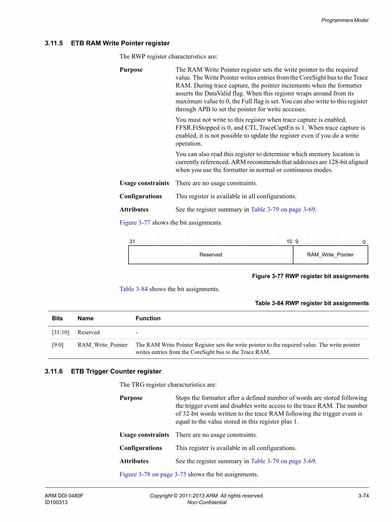
Programmers Model
3.11.5 ETB RAM Write Pointer register
The RWP register characteristics are:
Purpose The RAM Write Pointer register sets the write pointer to the required value. The Write Pointer writes entries from the CoreSight bus to the Trace RAM. During trace capture, the pointer increments when the formatter asserts the DataValid flag. When this register wraps around from its maximum value to 0, the Full flag is set. You can also write to this register through APB to set the pointer for write accesses.You must not write to this register when trace capture is enabled, FFSR.FtStopped is 0, and CTL.TraceCaptEn is 1. When trace capture is enabled, it is not possible to update the register even if you do a write operation.You can also read this register to determine which memory location is currently referenced. ARM recommends that addresses are 128-bit aligned when you use the formatter in normal or continuous modes.
Usage constraints There are no usage constraints.
Configurations This register is available in all configurations.
Attributes See the register summary in Table 3-79 on page 3-69.
Figure 3-77 shows the bit assignments.
Figure 3-77 RWP register bit assignments
Table 3-84 shows the bit assignments.
3.11.6 ETB Trigger Counter register
The TRG register characteristics are:
Purpose Stops the formatter after a defined number of words are stored following the trigger event and disables write access to the trace RAM. The number of 32-bit words written to the trace RAM following the trigger event is equal to the value stored in this register plus 1.
Usage constraints There are no usage constraints.
Configurations This register is available in all configurations.
Attributes See the register summary in Table 3-79 on page 3-69.
Figure 3-78 on page 3-75 shows the bit assignments.
31 0
Reserved
10 9
RAM_Write_Pointer
Table 3-84 RWP register bit assignments
Bits Name Function
[31:10] Reserved -
[9:0] RAM_Write_Pointer The RAM Write Pointer Register sets the write pointer to the required value. The write pointer writes entries from the CoreSight bus to the Trace RAM.
ARM DDI 0480F Copyright © 2011-2013 ARM. All rights reserved. 3-74ID100313 Non-Confidential

Programmers Model
Figure 3-78 TRG register bit assignments
Table 3-85 shows the bit assignments.
3.11.7 ETB Control register
The CTL register characteristics are:
Purpose Controls trace capture by the ETB.
Usage constraints There are no usage constraints.
Configurations This register is available in all configurations.
Attributes See the register summary in Table 3-79 on page 3-69.
Figure 3-79 shows the bit assignments.
Figure 3-79 CTL register bit assignments
31 0
Reserved
10 9
Trigger_Counter
Table 3-85 TRG register bit assignments
Bits Name Function
[31:10] Reserved -
[9:0] Trigger_Counter The counter is used as follows: Trace after The counter is set to a large value, slightly less than the number of entries
in the RAM.Trace before The counter is set to a small value.Trace about The counter is set to half the depth of the trace RAM.You must not write to this register when trace capture is enabled, FFSR.FtStopped is 0, and CTL.TraceCaptEn is 1. When a write is attempted, then the register is not updated. A read operation is permitted when trace capture is enabled.
31 0
Reserved
1
TraceCaptEn
ARM DDI 0480F Copyright © 2011-2013 ARM. All rights reserved. 3-75ID100313 Non-Confidential

Programmers Model
Table 3-86 shows the bit assignments.
3.11.8 ETB RAM Write Data register
The RWD register characteristics are:
Purpose Provides data that writes to ETB Trace RAM.
Usage constraints There are no usage constraints.
Configurations This register is available in all configurations.
Attributes See the register summary in Table 3-79 on page 3-69.
Figure 3-80 shows the bit assignments.
Figure 3-80 RWD register bit assignments
Table 3-87 shows the bit assignments.
3.11.9 ETB Formatter and Flush Status Register
The FFSR characteristics are:
Purpose Indicates the implemented trigger counter multipliers and other supported features of the trigger system.
Table 3-86 CTL register bit assignments
Bits Name Function
[31:1] Reserved -
[0] TraceCaptEn ETB Trace Capture Enable. This is the master enable bit that sets FtStopped to HIGH when TraceCaptEn is LOW. When capture is disabled, any remaining data in the ATB formatter is stored to RAM. When all of the data is stored, the formatter outputs FtStopped. Capture is fully disabled, or complete, when FtStopped goes HIGH. See ETB Formatter and Flush Status Register.0 Disable trace capture.1 Enable trace capture.
31 0
RAM_Write_Data
Table 3-87 RWD register bit assignments
Bits Name Function
[31:0] RAM_Write_Data When CTL.TraceCaptEn is 0:• Writes to this register write the data to the ETB trace RAM. The RAM Write Pointer
Register value is incremented.• Reads of this register return an UNKNOWN value.When CTL.TraceCaptEn is 1:• Writes to this register are ignored. The data is not written to the ETB trace RAM and the
RAM Write Pointer is not affected.• Reads of this register return an UNKNOWN value.
ARM DDI 0480F Copyright © 2011-2013 ARM. All rights reserved. 3-76ID100313 Non-Confidential

Programmers Model
Usage constraints There are no usage constraints.
Configurations This register is available in all configurations.
Attributes See the register summary in Table 3-79 on page 3-69.
Figure 3-81 shows the bit assignments.
Figure 3-81 FFSR bit assignments
Table 3-88 shows the bit assignments.
3.11.10 ETB Formatter and Flush Control Register
The FFCR characteristics are:
Purpose Selects the formatter mode, and controls the generation of stop, trigger, and flush events.
Note To perform a stop on flush completion through a manually generated flush
request, two write operations to the register are required: • To enable the stop event, if it is not already enabled.• To generate the manual flush.
Usage constraints There are no usage constraints.
Configurations This register is available in all configurations.
Attributes See the register summary in Table 3-79 on page 3-69.
Figure 3-82 on page 3-78 shows the bit assignments.
31 0
Reserved
1
FlInProg
2
FtStopped
Table 3-88 FFSR bit assignments
Bits Name Function
[31:2] Reserved -
[1] FtStopped Formatter stopped. The formatter has received a stop request signal and all trace data and post-amble is sent. Any additional trace data on the ATB interface is ignored and atreadys goes HIGH.0 Formatter is not stopped.1 Formatter is stopped.
[0] FlInProg Flush In Progress. This is an indication of the current state of afvalids.0 afvalids is LOW.1 afvalids is HIGH.
ARM DDI 0480F Copyright © 2011-2013 ARM. All rights reserved. 3-77ID100313 Non-Confidential
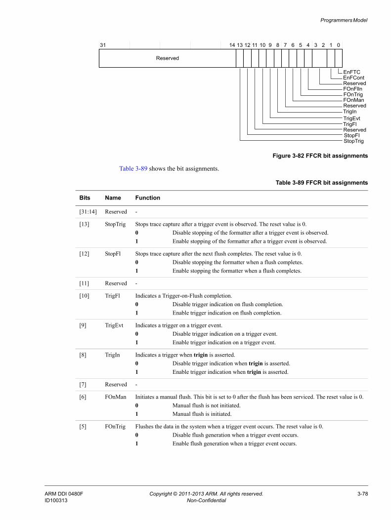
Programmers Model
Figure 3-82 FFCR bit assignments
Table 3-89 shows the bit assignments.
31 14 13 12 11 10 9 8 7 6 5 4 3 2 1 0
Reserved
EnFTCEnFContReservedFOnFllnFOnTrigFOnManReserved
TrigEvtTrigIn
TrigFlReservedStopFIStopTrig
Table 3-89 FFCR bit assignments
Bits Name Function
[31:14] Reserved -
[13] StopTrig Stops trace capture after a trigger event is observed. The reset value is 0.0 Disable stopping of the formatter after a trigger event is observed.1 Enable stopping of the formatter after a trigger event is observed.
[12] StopFl Stops trace capture after the next flush completes. The reset value is 0.0 Disable stopping the formatter when a flush completes.1 Enable stopping the formatter when a flush completes.
[11] Reserved -
[10] TrigFl Indicates a Trigger-on-Flush completion.0 Disable trigger indication on flush completion.1 Enable trigger indication on flush completion.
[9] TrigEvt Indicates a trigger on a trigger event.0 Disable trigger indication on a trigger event.1 Enable trigger indication on a trigger event.
[8] TrigIn Indicates a trigger when trigin is asserted.0 Disable trigger indication when trigin is asserted.1 Enable trigger indication when trigin is asserted.
[7] Reserved -
[6] FOnMan Initiates a manual flush. This bit is set to 0 after the flush has been serviced. The reset value is 0.0 Manual flush is not initiated.1 Manual flush is initiated.
[5] FOnTrig Flushes the data in the system when a trigger event occurs. The reset value is 0.0 Disable flush generation when a trigger event occurs.1 Enable flush generation when a trigger event occurs.
ARM DDI 0480F Copyright © 2011-2013 ARM. All rights reserved. 3-78ID100313 Non-Confidential

Programmers Model
3.11.11 Integration Test Miscellaneous Output register 0
The ITMISCOP0 register characteristics are:
Purpose Controls the values of some outputs from the ETB.
Usage constraints There are no usage constraints.
Configurations This register is available in all configurations.
Attributes See the register summary in Table 3-79 on page 3-69.
Figure 3-83 shows the bit assignments.
Figure 3-83 ITMISCOP0 register bit assignments
[4] FOnFlIn Enables use of the flushin input. The reset value is 0.0 Disable flush generation using the flushin interface.1 Enable flush generation using the flushin interface.
[3:2] Reserved -
[1] EnFCont When EnFTC is 1, this bit controls whether triggers are recorded in the trace stream. Most usage models require Continuous mode, where this bit is set to 1. The reset value is 0. See Modes of operation on page 10-5 for more information.
Note This bit can only be changed when FtStopped is HIGH.
0 Triggers are not embedded in the trace stream.1 Triggers are embedded in the trace stream.
[0] EnFTC Enable formatting. Most usage models require Continuous mode, where this bit is set to 1. The reset value is 0. See Modes of operation on page 10-5 for more information.
Note This bit can only be changed when FtStopped is HIGH.
0 Formatting is disabled.1 Formatting is enabled.
Table 3-89 FFCR bit assignments (continued)
Bits Name Function
FULL
31 1 0
Reserved
ACQCOMP
2
ARM DDI 0480F Copyright © 2011-2013 ARM. All rights reserved. 3-79ID100313 Non-Confidential

Programmers Model
Table 3-90 shows the bit assignments.
3.11.12 Integration Test Trigger In and Flush In Acknowledge register
The ITTRFLINACK register characteristics are:
Purpose Enables control of the triginack and flushinack outputs from the ETB.
Usage constraints There are no usage constraints.
Configurations This register is available in all configurations.
Attributes See the register summary in Table 3-79 on page 3-69.
Figure 3-84 shows the bit assignments.
Figure 3-84 ITTRFLINACK register bit assignments
Table 3-91 shows the bit assignments.
Table 3-90 ITMISCOP0 register bit assignments
Bits Name Function
[31:2] Reserved -
[1] FULL Sets the value of full output.0 Sets the value to 0.1 Sets the value to 1.
[0] ACQCOMP Sets the value of acqcomp output.0 Sets the value to 0.1 Sets the value to 1.
31 0
Reserved
FLUSHINACK
2 1
TRIGINACK
Table 3-91 ITTRFLINACK register bit assignments
Bits Name Function
[31:2] Reserved -
[1] FLUSHINACK Sets the value of flushinack.0 Sets the value of FLUSHINACK to 0.1 Sets the value of FLUSHINACK to 1.
[0] TRIGINACK Sets the value of triginack.0 Sets the value of TRIGINACK to 0.1 Sets the value of TRIGINACK to 1.
ARM DDI 0480F Copyright © 2011-2013 ARM. All rights reserved. 3-80ID100313 Non-Confidential

Programmers Model
3.11.13 Integration Test Trigger In and Flush In register
The ITTRFLIN register characteristics are:
Purpose Contains the values of the flushin and trigin inputs to the ETB.
Usage constraints There are no usage constraints.
Configurations This register is available in all configurations.
Attributes See the register summary in Table 3-79 on page 3-69.
Figure 3-85 shows the bit assignments.
Figure 3-85 ITTRFLIN register bit assignments
Table 3-92 shows the bit assignments.
3.11.14 Integration Test ATB Data register 0
The ITATBDATA0 register characteristics are:
Purpose Contains the value of the atdatas inputs to the ETB. The values are only valid when atvalids is HIGH.
Usage constraints There are no usage constraints.
Configurations This register is available in all configurations.
Attributes See the register summary in Table 3-79 on page 3-69.
Figure 3-86 on page 3-82 shows the bit assignments.
FLUSHIN
31 1 0
Reserved
TRIGIN
2
Table 3-92 ITTRFLIN register bit assignments
Bits Name Function
[31:2] Reserved -
[1] FLUSHIN Reads the value of flushin.0 flushin is LOW.1 flushin is HIGH.
[0] TRIGIN Reads the value of trigin.0 trigin is LOW.1 trigin is HIGH.
ARM DDI 0480F Copyright © 2011-2013 ARM. All rights reserved. 3-81ID100313 Non-Confidential

Programmers Model
Figure 3-86 ITATBDATA0 register bit assignments
Table 3-93 shows the bit assignments.
3.11.15 Integration Test ATB Control Register 2
The ITATBCTR2 characteristics are:
Purpose Enables control of the atreadys and afvalids outputs of the ETB.
Usage constraints There are no usage constraints.
Configurations This register is available in all configurations.
Attributes See the register summary in Table 3-79 on page 3-69.
Figure 3-87 on page 3-83 shows the bit assignments.
31 5 4 1 0
Reserved
23
ATDATA0ATDATA7ATDATA15ATDATA23ATDATA31
Table 3-93 ITATBDATA0 register bit assignments
Bits Name Function
[31:5] Reserved -
[4] ATDATA_31 Reads the value of atdatas[31].0 atdatas[31] is 0.1 atdatas[31] is 1.
[3] ATDATA_23 Reads the value of atdatas[23].0 atdatas[23] is 0.1 atdatas[23] is 1.
[2] ATDATA_15 Reads the value of atdatas[15].0 atdatas[15] is 0.1 atdatas[15] is 1.
[1] ATDATA_7 Readsthe value of atdatas[7].0 atdatas[7] is 0.1 atdatas[7] is 1.
[0] ATDATA_0 Reads the value of atdatas[0]. 0 atdatas[0] is 0.1 atdatas[0] is 1.
ARM DDI 0480F Copyright © 2011-2013 ARM. All rights reserved. 3-82ID100313 Non-Confidential
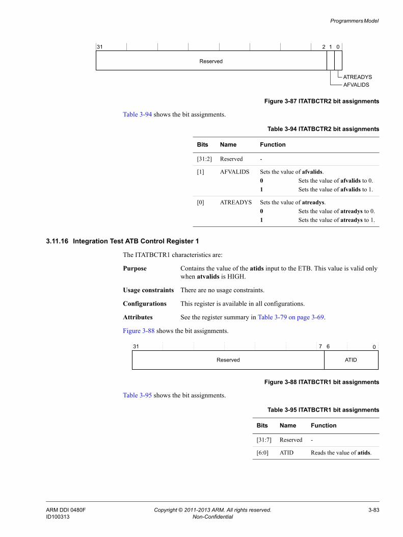
Programmers Model
Figure 3-87 ITATBCTR2 bit assignments
Table 3-94 shows the bit assignments.
3.11.16 Integration Test ATB Control Register 1
The ITATBCTR1 characteristics are:
Purpose Contains the value of the atids input to the ETB. This value is valid only when atvalids is HIGH.
Usage constraints There are no usage constraints.
Configurations This register is available in all configurations.
Attributes See the register summary in Table 3-79 on page 3-69.
Figure 3-88 shows the bit assignments.
Figure 3-88 ITATBCTR1 bit assignments
Table 3-95 shows the bit assignments.
AFVALIDS
31 1 0
Reserved
ATREADYS
2
Table 3-94 ITATBCTR2 bit assignments
Bits Name Function
[31:2] Reserved -
[1] AFVALIDS Sets the value of afvalids.0 Sets the value of afvalids to 0.1 Sets the value of afvalids to 1.
[0] ATREADYS Sets the value of atreadys.0 Sets the value of atreadys to 0.1 Sets the value of atreadys to 1.
31 0
Reserved
7 6
ATID
Table 3-95 ITATBCTR1 bit assignments
Bits Name Function
[31:7] Reserved -
[6:0] ATID Reads the value of atids.
ARM DDI 0480F Copyright © 2011-2013 ARM. All rights reserved. 3-83ID100313 Non-Confidential
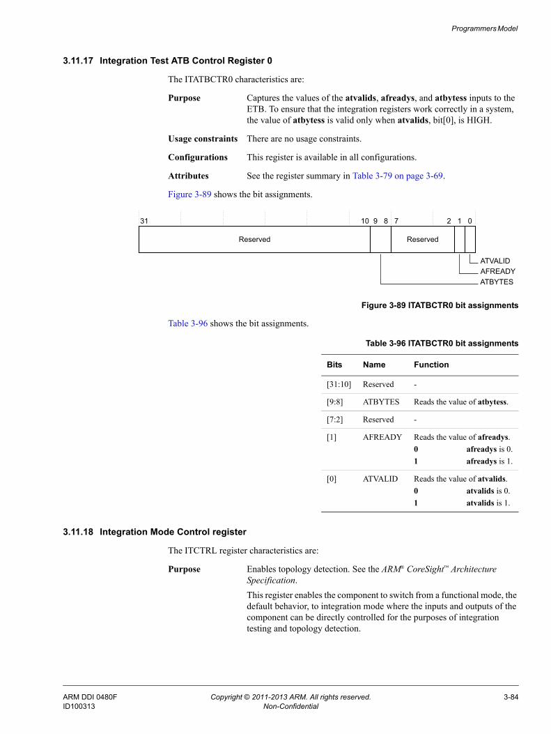
Programmers Model
3.11.17 Integration Test ATB Control Register 0
The ITATBCTR0 characteristics are:
Purpose Captures the values of the atvalids, afreadys, and atbytess inputs to the ETB. To ensure that the integration registers work correctly in a system, the value of atbytess is valid only when atvalids, bit[0], is HIGH.
Usage constraints There are no usage constraints.
Configurations This register is available in all configurations.
Attributes See the register summary in Table 3-79 on page 3-69.
Figure 3-89 shows the bit assignments.
Figure 3-89 ITATBCTR0 bit assignments
Table 3-96 shows the bit assignments.
3.11.18 Integration Mode Control register
The ITCTRL register characteristics are:
Purpose Enables topology detection. See the ARM® CoreSight™ Architecture Specification.This register enables the component to switch from a functional mode, the default behavior, to integration mode where the inputs and outputs of the component can be directly controlled for the purposes of integration testing and topology detection.
31 0
Reserved
7 2
Reserved
10 9 8 1
AFREADYATVALID
ATBYTES
Table 3-96 ITATBCTR0 bit assignments
Bits Name Function
[31:10] Reserved -
[9:8] ATBYTES Reads the value of atbytess.
[7:2] Reserved -
[1] AFREADY Reads the value of afreadys.0 afreadys is 0.1 afreadys is 1.
[0] ATVALID Reads the value of atvalids.0 atvalids is 0.1 atvalids is 1.
ARM DDI 0480F Copyright © 2011-2013 ARM. All rights reserved. 3-84ID100313 Non-Confidential

Programmers Model
Note When a device is in integration mode, the intended functionality might not
be available.
After performing integration or topology detection, you must reset the system to ensure correct behavior of CoreSight and other connected system components that the integration or topology detection can affect.
Usage constraints There are no usage constraints.
Configurations This register is available in all configurations.
Attributes See the register summary in Table 3-79 on page 3-69.
Figure 3-90 shows the bit assignments.
Figure 3-90 ITCTRL register bit assignments
Table 3-97 shows the bit assignments.
3.11.19 Claim Tag Set register
The CLAIMSET register characteristics are:
Purpose Software can use the claim tag to coordinate application and debugger access to trace unit functionality. The claim tags have no effect on the operation of the component. The CLAIMSET register sets bits in the claim tag, and determines the number of claim bits implemented.
Usage constraints There are no usage constraints.
Configurations This register is available in all configurations.
Attributes See the register summary in Table 3-79 on page 3-69.
Figure 3-91 shows the bit assignments.
Figure 3-91 CLAIMSET register bit assignments
31 1 0
Reserved
IME
Table 3-97 ITCTRL register bit assignments
Bits Name Function
[31:1] Reserved -
[0] IME Integration Mode Enable.0 Disable integration mode.1 Enable integration mode.
Reserved
31 4 3 0
SET
ARM DDI 0480F Copyright © 2011-2013 ARM. All rights reserved. 3-85ID100313 Non-Confidential

Programmers Model
Table 3-98 shows the bit assignments.
3.11.20 Claim Tag Clear register
The CLAIMCLR register characteristics are:
Purpose Software can use the claim tag to coordinate application and debugger access to trace unit functionality. The claim tags have no effect on the operation of the component. The CLAIMCLR register sets the bits in the claim tag to 0 and determines the current value of the claim tag.
Usage constraints There are no usage constraints.
Configurations This register is available in all configurations.
Attributes See the register summary in Table 3-79 on page 3-69.
Figure 3-92 shows the bit assignments.
Figure 3-92 CLAIMCLR register bit assignments
Table 3-99 shows the bit assignments.
3.11.21 Lock Access Register
The LAR characteristics are:
Purpose Controls write access from self-hosted, on-chip accesses. The LAR does not affect the accesses that are using the external debugger interface.
Table 3-98 CLAIMSET register bit assignments
Bits Name Function
[31:4] Reserved -
[3:0] SET On reads, for each bit: 1 Claim tag bit is implemented.On writes, for each bit:0 Has no effect.1 Sets the relevant bit of the claim tag.
Reserved
31 4 3 0
CLR
Table 3-99 CLAIMCLR register bit assignments
Bits Name Function
[31:4] Reserved -
[3:0] CLR On reads, for each bit: 0 Claim tag bit is not set.1 Claim tag bit is set.On writes, for each bit: 0 Has no effect.1 Clears the relevant bit of the claim tag.
ARM DDI 0480F Copyright © 2011-2013 ARM. All rights reserved. 3-86ID100313 Non-Confidential

Programmers Model
Usage constraints There are no usage constraints.
Configurations This register is available in all configurations.
Attributes See the register summary in Table 3-79 on page 3-69.
Figure 3-93 shows the bit assignments.
Figure 3-93 LAR bit assignments
Table 3-100 shows the bit assignments.
3.11.22 Lock Status Register
The LSR characteristics are:
Purpose Indicates the status of the lock control mechanism. This lock prevents accidental writes. When locked, write accesses are denied for all registers except for the LAR. The lock registers do not affect accesses from the external debug interface. This register reads as 0 when accessed from the external debug interface.
Usage constraints There are no usage constraints.
Configurations This register is available in all configurations.
Attributes See the register summary in Table 3-79 on page 3-69.
Figure 3-94 shows the bit assignments.
Figure 3-94 LSR bit assignments
31 0
KEY
Table 3-100 LAR bit assignments
Bits Name Function
[31:0] KEY Software lock key value. 0xC5ACCE55 Clear the software lock.All other write values set the software lock.
Reserved
31 03 12
SLISLKnTT
ARM DDI 0480F Copyright © 2011-2013 ARM. All rights reserved. 3-87ID100313 Non-Confidential

Programmers Model
Table 3-101 shows the bit assignments.
3.11.23 Authentication Status register
The AUTHSTATUS register characteristics are:
Purpose Reports the required security level and present status.
Usage constraints There are no usage constraints.
Configurations This register is available in all configurations.
Attributes See the register summary in Table 3-79 on page 3-69.
Figure 3-95 shows the bit assignments.
Figure 3-95 AUTHSTATUS register bit assignments
Table 3-102 shows the bit assignments.
Table 3-101 LSR bit assignments
Bits Name Function
[31:3] Reserved -
[2] nTT Register size indicator. Always 0. Indicates that the LAR is implemented as 32-bit.
[1] SLK Software Lock Status. Returns the present lock status of the device, from the current interface.0 Indicates that write operations are permitted from this interface.1 Indicates that write operations are not permitted from this interface. Read
operations are permitted.
[0] SLI Software Lock Implemented. Indicates that a lock control mechanism is present from this interface.0 Indicates that a lock control mechanism is not present from this interface. Write
operations to the LAR are ignored.1 Indicates that a lock control mechanism is present from this interface.
31 8 7 6 5 4 3 2 0
Reserved
NSIDNSNIDSIDSNID
1
Table 3-102 AUTHSTATUS register bit assignments
Bits Name Function
[31:8] Reserved -
[7:6] SNID Indicates the security level for secure non-invasive debug:0b00 Functionality is not implemented or is controlled elsewhere.
ARM DDI 0480F Copyright © 2011-2013 ARM. All rights reserved. 3-88ID100313 Non-Confidential

Programmers Model
3.11.24 Device Configuration register
The DEVID register characteristics are:
Purpose Indicates the capabilities of the component.
Usage constraints There are no usage constraints.
Configurations This register is available in all configurations.
Attributes See the register summary in Table 3-79 on page 3-69.
Figure 3-96 shows the bit assignments.
Figure 3-96 DEVID register bit assignments
Table 3-103 shows the DEVID register bit assignments.
3.11.25 Device Type Identifier register
The DEVTYPE register characteristics are:
Purpose Provides a debugger with information about the component when the Part Number field is not recognized. The debugger can then report this information.
[5:4] SID Indicates the security level for secure invasive debug:0b00 Functionality is not implemented or is controlled elsewhere.
[3:2] NSNID Indicates the security level for non-secure non-invasive debug:0b00 Functionality is not implemented or is controlled elsewhere.
[1:0] NSID Indicates the security level for non-secure invasive debug:0b00 Functionality is not implemented or is controlled elsewhere.
Table 3-102 AUTHSTATUS register bit assignments (continued)
Bits Name Function
31 6 5 4
Reserved
0
RAMCLKEXTMUXNUM
Table 3-103 DEVID register bit assignments
Bits Name Function
[31:6] Reserved -
[5] RAMCLK This bit returns 0 on reads to indicate that the ETB RAM operates synchronously to atclk. 0 The ETB RAM operates synchronously to atclk.
[4:0] EXTMUXNUM Number of external multiplexing available. Non-zero values indicate the type of ATB multiplexing on the input to the ATB.0b0000 Only 0x00 is supported, that is, no multiplexing is present. This value helps detect
the ATB structure.
ARM DDI 0480F Copyright © 2011-2013 ARM. All rights reserved. 3-89ID100313 Non-Confidential
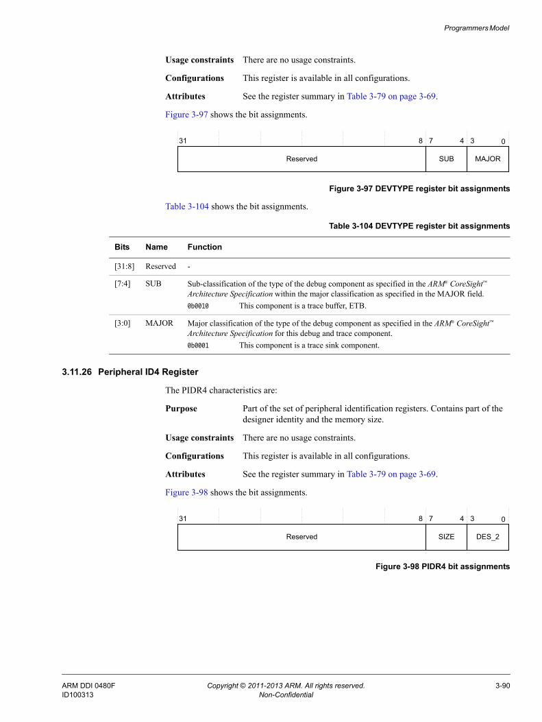
Programmers Model
Usage constraints There are no usage constraints.
Configurations This register is available in all configurations.
Attributes See the register summary in Table 3-79 on page 3-69.
Figure 3-97 shows the bit assignments.
Figure 3-97 DEVTYPE register bit assignments
Table 3-104 shows the bit assignments.
3.11.26 Peripheral ID4 Register
The PIDR4 characteristics are:
Purpose Part of the set of peripheral identification registers. Contains part of the designer identity and the memory size.
Usage constraints There are no usage constraints.
Configurations This register is available in all configurations.
Attributes See the register summary in Table 3-79 on page 3-69.
Figure 3-98 shows the bit assignments.
Figure 3-98 PIDR4 bit assignments
31 0
Reserved
7
SUB
8 4
MAJOR
3
Table 3-104 DEVTYPE register bit assignments
Bits Name Function
[31:8] Reserved -
[7:4] SUB Sub-classification of the type of the debug component as specified in the ARM® CoreSight™ Architecture Specification within the major classification as specified in the MAJOR field.0b0010 This component is a trace buffer, ETB.
[3:0] MAJOR Major classification of the type of the debug component as specified in the ARM® CoreSight™ Architecture Specification for this debug and trace component.0b0001 This component is a trace sink component.
31 0
Reserved
7
SIZE
8 4
DES_2
3
ARM DDI 0480F Copyright © 2011-2013 ARM. All rights reserved. 3-90ID100313 Non-Confidential

Programmers Model
Table 3-105 shows the bit assignments.
3.11.27 Peripheral ID0 Register
The PIDR0 characteristics are:
Purpose Part of the set of peripheral identification registers. Contains part of the designer-specific part number.
Usage constraints There are no usage constraints.
Configurations This register is available in all configurations.
Attributes See the register summary in Table 3-79 on page 3-69.
Figure 3-99 shows the bit assignments.
Figure 3-99 PIDR0 bit assignments
Table 3-106 shows the bit assignments.
3.11.28 Peripheral ID1 Register
The PIDR1 characteristics are:
Purpose Part of the set of peripheral identification registers. Contains part of the designer-specific part number and part of the designer identity.
Usage constraints There are no usage constraints.
Configurations This register is available in all configurations.
Attributes See the register summary in Table 3-79 on page 3-69.
Table 3-105 PIDR4 bit assignments
Bits Name Function
[31:8] Reserved -
[7:4] SIZE Always 0b0000. Indicates that the device only occupies 4KB of memory.
[3:0] DES_2 Together, PIDR1.DES_0, PIDR2.DES_1, and PIDR4.DES_2 identify the designer of the component.0b0100 JEDEC continuation code.
31 0
Reserved
78
PART_0
Table 3-106 PIDR0 bit assignments
Bits Name Function
[31:8] Reserved -
[7:0] PART_0 Bits[7:0] of the 12-bit part number of the component. The designer of the component assigns this part number.0x07 Indicates bits[7:0] of the part number of the component.
ARM DDI 0480F Copyright © 2011-2013 ARM. All rights reserved. 3-91ID100313 Non-Confidential

Programmers Model
Figure 3-100 shows the bit assignments.
Figure 3-100 PIDR1 bit assignments
Table 3-107 shows the PIDR1 bit assignments.
3.11.29 Peripheral ID2 Register
The PIDR2 characteristics are:
Purpose Part of the set of peripheral identification registers. Contains part of the designer identity and the product revision.
Usage constraints There are no usage constraints.
Configurations This register is available in all configurations.
Attributes See the register summary in Table 3-79 on page 3-69.
Figure 3-101 shows the bit assignments.
Figure 3-101 PIDR2 bit assignments
Table 3-108 shows the bit assignments.
31 0
Reserved
78
PART_1
4 3
DES_0
Table 3-107 PIDR1 bit assignments
Bits Name Function
[31:8] Reserved -
[7:4] DES_0 Together, PIDR1.DES_0, PIDR2.DES_1, and PIDR4.DES_2 identify the designer of the component.0b1011 ARM. Bits[3:0] of the JEDEC JEP106 Identity Code.
[3:0] PART_1 Bits[11:8] of the 12-bit part number of the component. The designer of the component assigns this part number.0b1001 Indicates bits[11:8] of the part number of the component.
31 0
Reserved
7
REVISION
8 4
DES_1
3 2
JEDEC
Table 3-108 PIDR2 bit assignments
Bits Name Function
[31:8] Reserved -
ARM DDI 0480F Copyright © 2011-2013 ARM. All rights reserved. 3-92ID100313 Non-Confidential

Programmers Model
3.11.30 Peripheral ID3 Register
The PIDR3 characteristics are:
Purpose Part of the set of peripheral identification registers. Contains the REVAND and CMOD fields.
Usage constraints There are no usage constraints.
Configurations This register is available in all configurations.
Attributes See the register summary in Table 3-79 on page 3-69.
Figure 3-102 shows the bit assignments.
Figure 3-102 PIDR3 bit assignments
Table 3-109 shows the bit assignments.
3.11.31 Component ID0 Register
The CIDR0 characteristics are:
Purpose A component identification register that indicates the presence of identification registers.
Usage constraints There are no usage constraints.
Configurations This register is available in all configurations.
Attributes See the register summary in Table 3-79 on page 3-69.
[7:4] REVISION 0b0011 This device is at r0p4.
[3] JEDEC Always 1. Indicates that the JEDEC-assigned designer ID is used.
[2:0] DES_1 Together, PIDR1.DES_0, PIDR2.DES_1, and PIDR4.DES_2 identify the designer of the component.0b011 ARM. Bits[6:4] of the JEDEC JEP106 Identity Code.
Table 3-108 PIDR2 bit assignments (continued)
Bits Name Function
31 0
Reserved
7
REVAND
8 4
CMOD
3
Table 3-109 PIDR3 bit assignments
Bits Name Function
[31:8] Reserved -
[7:4] REVAND 0b0000 Indicates that there are no errata fixes to this component.
[3:0] CMOD Customer Modified. Indicates whether the customer has modified the behavior of the component. In most cases, this field is 0b0000. Customers change this value when they make authorized modifications to this component.0b0000 Indicates that the customer has not modified this component.
ARM DDI 0480F Copyright © 2011-2013 ARM. All rights reserved. 3-93ID100313 Non-Confidential

Programmers Model
Figure 3-103 shows the bit assignments.
Figure 3-103 CIDR0 bit assignments
Table 3-110 shows the bit assignments.
3.11.32 Component ID1 Register
The CIDR1 characteristics are:
Purpose A component identification register that indicates the presence of identification registers. This register also indicates the component class.
Usage constraints There are no usage constraints.
Configurations This register is available in all configurations.
Attributes See the register summary in Table 3-79 on page 3-69.
Figure 3-104 shows the bit assignments.
Figure 3-104 CIDR1 bit assignments
Table 3-111 shows the bit assignments.
PRMBL_0
31 8 7 0
Reserved
Table 3-110 CIDR0 bit assignments
Bits Name Function
[31:8] Reserved -
[7:0] PRMBL_0 Preamble[0]. Contains bits[7:0] of the component identification code.0x0D Bits[7:0] of the identification code.
31 8 7 4 3 0
PRMBL_1CLASSReserved
Table 3-111 CIDR1 bit assignments
Bits Name Function
[31:8] Reserved -
[7:4] CLASS Class of the component, for example, whether the component is a ROM table or a generic CoreSight SoC-400 component. Contains bits[15:12] of the component identification code.0b1001 Indicates that the component is a CoreSight SoC-400 component.
[3:0] PRMBL_1 Preamble[1]. Contains bits[11:8] of the component identification code.0b0000 Bits[11:8] of the identification code.
ARM DDI 0480F Copyright © 2011-2013 ARM. All rights reserved. 3-94ID100313 Non-Confidential

Programmers Model
3.11.33 Component ID2 Register
The CIDR2 characteristics are:
Purpose A component identification register that indicates the presence of identification registers.
Usage constraints There are no usage constraints.
Configurations This register is available in all configurations.
Attributes See the register summary in Table 3-79 on page 3-69.
Figure 3-105 shows the bit assignments.
Figure 3-105 CIDR2 bit assignments
Table 3-112 shows the bit assignments.
3.11.34 Component ID3 Register
The CIDR3 characteristics are:
Purpose A component identification register that indicates the presence of identification registers.
Usage constraints There are no usage constraints.
Configurations This register is available in all configurations.
Attributes See the register summary in Table 3-79 on page 3-69.
Figure 3-106 shows the bit assignments.
Figure 3-106 CIDR3 bit assignments
PRMBL_2
31 8 7 0
Reserved
Table 3-112 CIDR2 bit assignments
Bits Name Function
[31:8] Reserved -
[7:0] PRMBL_2 Preamble[2]. Contains bits[23:16] of the component identification code.0x05 Bits[23:16] of the identification code.
31 0
Reserved
78
PRMBL_3
ARM DDI 0480F Copyright © 2011-2013 ARM. All rights reserved. 3-95ID100313 Non-Confidential

Programmers Model
Table 3-113 shows the bit assignments.
Table 3-113 CIDR3 bit assignments
Bits Name Function
[31:8] Reserved -
[7:0] PRMBL_3 Preamble[3]. Contains bits[31:24] of the component identification code.0xB1 Bits[31:24] of the identification code.
ARM DDI 0480F Copyright © 2011-2013 ARM. All rights reserved. 3-96ID100313 Non-Confidential

Programmers Model
3.12 TPIU register summaryTable 3-114 shows the TPIU registers in offset order from the base memory address.
Table 3-114 TPIU register summary
Offset Name Type Reset Description
0x000 Supported_Port_Sizes RO 0x00000001 Supported Port Size register on page 3-99
0x004 Current_port_size RW 0x00000001 Current Port Size register on page 3-103
0x100 Supported_trigger_modes RO 0x0000011F Supported Trigger Modes register on page 3-107
0x104 Trigger_counter_value RW 0x00000000 Trigger Counter Value register on page 3-108
0x108 Trigger_multiplier RW 0x00000000 Trigger Multiplier register on page 3-109
0x200 Supported_test_pattern_modes RO 0x0003000F Supported Test Patterns/Modes register on page 3-110
0x204 Current_test_pattern_mode RW 0x00000000 Current Test Pattern/Modes register on page 3-111
0x208 TPRCR RW 0x00000000 TPIU Test Pattern Repeat Counter Register on page 3-112
0x300 FFSR RO 0x00000000 Formatter and Flush Status Register on page 3-113
0x304 FFCR RW 0x00000000 Formatter and Flush Control Register on page 3-114
0x308 FSCR RW 0x00000040 Formatter Synchronization Counter Register on page 3-116
0x400 EXTCTL_In_Port RO 0x00000000 TPIU EXCTL In Port register on page 3-117
0x404 EXTCTL_Out_Port RW 0x00000000 TPIU EXCTL Out Port register on page 3-118
0xEE4 ITTRFLINACK WO 0x00000000 Integration Test Trigger In and Flush In Acknowledge register on page 3-118
0xEE8 ITTRFLIN RO 0x00000000 Integration Test Trigger In and Flush In register on page 3-119
0xEEC ITATBDATA0 RO 0x00000000 Integration Test ATB Data register 0 on page 3-120
0xEF0 ITATBCTR2 WO 0x00000000 Integration Test ATB Control Register 2 on page 3-121
0xEF4 ITATBCTR1 RO 0x00000000 Integration Test ATB Control Register 1 on page 3-121
0xEF8 ITATBCTR0 RO 0x00000000 Integration Test ATB Control Register 0 on page 3-122
0xF00 ITCTRL RW 0x00000000 Integration Mode Control register on page 3-123
0xFA0 CLAIMSET RW 0x0000000F Claim Tag Set register on page 3-124
0xFA4 CLAIMCLR RW 0x00000000 Claim Tag Clear register on page 3-124
0xFB0 LAR WO 0x00000000 Lock Access Register on page 3-125
0xFB4 LSR RO 0x00000003 Lock Status Register on page 3-125
0xFB8 AUTHSTATUS RO 0x00000000 Authentication Status register on page 3-126
0xFC8 DEVID RO 0x000000A0 Device Configuration register on page 3-127
0xFCC DEVTYPE RO 0x00000011 Device Type Identifier register on page 3-128
0xFD0 PIDR4 RO 0x00000004 Peripheral ID4 Register on page 3-129
0xFD4 - - - Reserved
0xFD8 - - - Reserved
ARM DDI 0480F Copyright © 2011-2013 ARM. All rights reserved. 3-97ID100313 Non-Confidential

Programmers Model
0xFDC - - - Reserved
0xFE0 PIDR0 RO 0x00000012 Peripheral ID0 Register on page 3-129
0xFE4 PIDR1 RO 0x000000B9 Peripheral ID1 Register on page 3-130
0xFE8 PIDR2 RO 0x0000004B Peripheral ID2 Register on page 3-130
0xFEC PIDR3 RO 0x00000000 Peripheral ID3 Register on page 3-131
0xFF0 CIDR0 RO 0x0000000D Component ID0 Register on page 3-132
0xFF4 CIDR1 RO 0x00000090 Component ID1 Register on page 3-132
0xFF8 CIDR2 RO 0x00000005 Component ID2 Register on page 3-133
0xFFC CIDR3 RO 0x000000B1 Component ID3 Register on page 3-133
Table 3-114 TPIU register summary (continued)
Offset Name Type Reset Description
ARM DDI 0480F Copyright © 2011-2013 ARM. All rights reserved. 3-98ID100313 Non-Confidential

Programmers Model
3.13 TPIU register descriptionsThis section describes the TPIU registers. Table 3-114 on page 3-97 provides cross-references to individual registers.
3.13.1 Supported Port Size register
The Supported_Port_Sizes register characteristics are:
Purpose Each bit location is a single port size that is supported on the device, that is, 32-1 in bit locations [31:0]. When the bit is set then that port size is permitted. By default the RTL is designed to support all port sizes, set to 0xFFFFFFFF. The value returned by this register is controlled by the input tie-off tpmaxdatasize. The external tie-off, tpmaxdatasize, must be set during finalization of the ASIC to reflect the actual number of tracedata signals being wired to physical pins. This is to ensure that tools do not attempt to select a port width that cannot be captured by an attached TPA. The value on tpmaxdatasize causes bits within the Supported Port Size register that represent wider widths to be clear, that is, unsupported.
Usage constraints There are no usage constraints.
Configurations This register is available in all configurations.
Attributes See the register summary in Table 3-114 on page 3-97.
Figure 3-107 on page 3-100 shows the bit assignments.
ARM DDI 0480F Copyright © 2011-2013 ARM. All rights reserved. 3-99ID100313 Non-Confidential

Programmers Model
Figure 3-107 Supported_Port_Sizes register bit assignments
Table 3-115 shows the bit assignments.
31 30 29 28 27 26 25 24 23 22 21 20 19 18 17 16 15 14 13 12 11 10 9 8 7 6 5 4 3 2 1 0
PORT_SIZE_3PORT_SIZE_2PORT_SIZE_1
PORT_SIZE_4PORT_SIZE_5
PORT_SIZE_8PORT_SIZE_7PORT_SIZE_6
PORT_SIZE_11PORT_SIZE_10PORT_SIZE_9
PORT_SIZE_12PORT_SIZE_13
PORT_SIZE_16PORT_SIZE_15PORT_SIZE_14
PORT_SIZE_19PORT_SIZE_18PORT_SIZE_17
PORT_SIZE_20PORT_SIZE_21
PORT_SIZE_24PORT_SIZE_23PORT_SIZE_22
PORT_SIZE_27PORT_SIZE_26PORT_SIZE_25
PORT_SIZE_28PORT_SIZE_29
PORT_SIZE_32PORT_SIZE_31PORT_SIZE_30
Table 3-115 Supported_Port_Sizes register bit assignments
Bits Name Function
[31] PORT_SIZE_32 Indicates whether the TPIU supports port size of 32-bit.0 Port size is not supported.1 Port size is supported.
[30] PORT_SIZE_31 Indicates whether the TPIU supports port size of 31-bit.0 Port size is not supported.1 Port size is supported.
[29] PORT_SIZE_30 Indicates whether the TPIU supports port size of 30-bit.0 Port size is not supported.1 Port size is supported.
ARM DDI 0480F Copyright © 2011-2013 ARM. All rights reserved. 3-100ID100313 Non-Confidential

Programmers Model
[28] PORT_SIZE_29 Indicates whether the TPIU supports port size of 29-bit.0 Port size is not supported.1 Port size is supported.
[27] PORT_SIZE_28 Indicates whether the TPIU supports port size of 28-bit.0 Port size is not supported.1 Port size is supported.
[26] PORT_SIZE_27 Indicates whether the TPIU supports port size of 27-bit.0 Port size is not supported.1 Port size is supported.
[25] PORT_SIZE_26 Indicates whether the TPIU supports port size of 26-bit.0 Port size is not supported.1 Port size is supported.
[24] PORT_SIZE_25 Indicates whether the TPIU supports port size of 25-bit.0 Port size is not supported.1 Port size is supported.
[23] PORT_SIZE_24 Indicates whether the TPIU supports port size of 24-bit.0 Port size is not supported.1 Port size is supported.
[22] PORT_SIZE_23 Indicates whether the TPIU supports port size of 23-bit.0 Port size is not supported.1 Port size is supported.
[21] PORT_SIZE_22 Indicates whether the TPIU supports port size of 22-bit.0 Port size is not supported.1 Port size is supported.
[20] PORT_SIZE_21 Indicates whether the TPIU supports port size of 21-bit.0 Port size is not supported.1 Port size is supported.
[19] PORT_SIZE_20 Indicates whether the TPIU supports port size of 20-bit.0 Port size is not supported.1 Port size is supported.
[18] PORT_SIZE_19 Indicates whether the TPIU supports port size of 19-bit.0 Port size is not supported.1 Port size is supported.
[17] PORT_SIZE_18 Indicates whether the TPIU supports port size of 18-bit.0 Port size is not supported.1 Port size is supported.
[16] PORT_SIZE_17 Indicates whether the TPIU supports port size of 17-bit.0 Port size is not supported.1 Port size is supported.
Table 3-115 Supported_Port_Sizes register bit assignments (continued)
Bits Name Function
ARM DDI 0480F Copyright © 2011-2013 ARM. All rights reserved. 3-101ID100313 Non-Confidential

Programmers Model
[15] PORT_SIZE_16 Indicates whether the TPIU supports port size of 16-bit.0 Port size is not supported.1 Port size is supported.
[14] PORT_SIZE_15 Indicates whether the TPIU supports port size of 15-bit.0 Port size is not supported.1 Port size is supported.
[13] PORT_SIZE_14 Indicates whether the TPIU supports port size of 14-bit.0 Port size is not supported.1 Port size is supported.
[12] PORT_SIZE_13 Indicates whether the TPIU supports port size of 13-bit.0 Port size is not supported.1 Port size is supported.
[11] PORT_SIZE_12 Indicates whether the TPIU supports port size of 12-bit.0 Port size is not supported.1 Port size is supported.
[10] PORT_SIZE_11 Indicates whether the TPIU supports port size of 11-bit.0 Port size is not supported.1 Port size is supported.
[9] PORT_SIZE_10 Indicates whether the TPIU supports port size of 10-bit.0 Port size is not supported.1 Port size is supported.
[8] PORT_SIZE_9 Indicates whether the TPIU supports port size of 9-bit.0 Port size is not supported.1 Port size is supported.
[7] PORT_SIZE_8 Indicates whether the TPIU supports port size of 8-bit.0 Port size is not supported.1 Port size is supported.
[6] PORT_SIZE_7 Indicates whether the TPIU supports port size of 7-bit.0 Port size is not supported.1 Port size is supported.
[5] PORT_SIZE_6 Indicates whether the TPIU supports port size of 6-bit.0 Port size is not supported.1 Port size is supported.
[4] PORT_SIZE_5 Indicates whether the TPIU supports port size of 5-bit.0 Port size is not supported.1 Port size is supported.
[3] PORT_SIZE_4 Indicates whether the TPIU supports port size of 4-bit.0 Port size is not supported.1 Port size is supported.
Table 3-115 Supported_Port_Sizes register bit assignments (continued)
Bits Name Function
ARM DDI 0480F Copyright © 2011-2013 ARM. All rights reserved. 3-102ID100313 Non-Confidential

Programmers Model
3.13.2 Current Port Size register
The Current_port_size register characteristics are:
Purpose Has the same format as the Supported Port Sizes register but only one bit is set, and all others must be 0. Writing values with more than one bit set or setting a bit that is not indicated as supported is not supported and causes UNPREDICTABLE behavior. On reset, this defaults to the smallest possible port size, 1 bit, that is, 0x00000001.
Note Do not modify the value while the Trace Port is still active, or without
correctly stopping the formatter. See Formatter and Flush Control Register on page 3-114. This can result in data not being aligned to the port width. For example, data on an 8-bit trace port might not be byte aligned.
Usage constraints There are no usage constraints.
Configurations This register is available in all configurations.
Attributes See the register summary in Table 3-114 on page 3-97.
Figure 3-108 on page 3-104 shows the bit assignments.
[2] PORT_SIZE_3 Indicates whether the TPIU supports port size of 3-bit.0 Port size is not supported.1 Port size is supported.
[1] PORT_SIZE_2 Indicates whether the TPIU supports port size of 2-bit.0 Port size is not supported.1 Port size is supported.
[0] PORT_SIZE_1 Indicates whether the TPIU supports port size of 1-bit. 0 Port size is not supported.1 Port size is supported.
Table 3-115 Supported_Port_Sizes register bit assignments (continued)
Bits Name Function
ARM DDI 0480F Copyright © 2011-2013 ARM. All rights reserved. 3-103ID100313 Non-Confidential

Programmers Model
Figure 3-108 Current_port_size register bit assignments
Table 3-116 shows the bit assignments.
31 30 29 28 27 26 25 24 23 22 21 20 19 18 17 16 15 14 13 12 11 10 9 8 7 6 5 4 3 2 1 0
PORT_SIZE_3PORT_SIZE_2PORT_SIZE_1
PORT_SIZE_4PORT_SIZE_5
PORT_SIZE_8PORT_SIZE_7PORT_SIZE_6
PORT_SIZE_11PORT_SIZE_10PORT_SIZE_9
PORT_SIZE_12PORT_SIZE_13
PORT_SIZE_16PORT_SIZE_15PORT_SIZE_14
PORT_SIZE_19PORT_SIZE_18PORT_SIZE_17
PORT_SIZE_20PORT_SIZE_21
PORT_SIZE_24PORT_SIZE_23PORT_SIZE_22
PORT_SIZE_27PORT_SIZE_26PORT_SIZE_25
PORT_SIZE_28PORT_SIZE_29
PORT_SIZE_32PORT_SIZE_31PORT_SIZE_30
Table 3-116 Current_port_size register bit assignments
Bits Name Function
[31] PORT_SIZE_32 Indicates whether the current port size of the TPIU is 32-bit.0 Current port size is not 32.1 Current port size is 32.
[30] PORT_SIZE_31 Indicates whether the current port size of the TPIU is 31-bit.0 Current port size is not 31.1 Current port size is 31.
[29] PORT_SIZE_30 Indicates whether the current port size of the TPIU is 30-bit.0 Current port size is not 30.1 Current port size is 30.
ARM DDI 0480F Copyright © 2011-2013 ARM. All rights reserved. 3-104ID100313 Non-Confidential
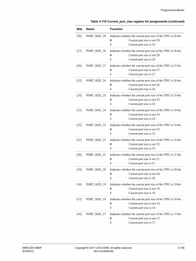
Programmers Model
[28] PORT_SIZE_29 Indicates whether the current port size of the TPIU is 29-bit.0 Current port size is not 29.1 Current port size is 29.
[27] PORT_SIZE_28 Indicates whether the current port size of the TPIU is 28-bit.0 Current port size is not 28.1 Current port size is 28.
[26] PORT_SIZE_27 Indicates whether the current port size of the TPIU is 27-bit.0 Current port size is not 27.1 Current port size is 27.
[25] PORT_SIZE_26 Indicates whether the current port size of the TPIU is 26-bit.0 Current port size is not 26.1 Current port size is 26.
[24] PORT_SIZE_25 Indicates whether the current port size of the TPIU is 25-bit.0 Current port size is not 25.1 Current port size is 25.
[23] PORT_SIZE_24 Indicates whether the current port size of the TPIU is 24-bit.0 Current port size is not 24.1 Current port size is 24.
[22] PORT_SIZE_23 Indicates whether the current port size of the TPIU is 23-bit.0 Current port size is not 23.1 Current port size is 23.
[21] PORT_SIZE_22 Indicates whether the current port size of the TPIU is 22-bit.0 Current port size is not 22.1 Current port size is 22.
[20] PORT_SIZE_21 Indicates whether the current port size of the TPIU is 21-bit.0 Current port size is not 21.1 Current port size is 21.
[19] PORT_SIZE_20 Indicates whether the current port size of the TPIU is 20-bit.0 Current port size is not 20.1 Current port size is 20.
[18] PORT_SIZE_19 Indicates whether the current port size of the TPIU is 19-bit.0 Current port size is not 19.1 Current port size is 19.
[17] PORT_SIZE_18 Indicates whether the current port size of the TPIU is 18-bit.0 Current port size is not 18.1 Current port size is 18.
[16] PORT_SIZE_17 Indicates whether the current port size of the TPIU is 17-bit.0 Current port size is not 17.1 Current port size is 17.
Table 3-116 Current_port_size register bit assignments (continued)
Bits Name Function
ARM DDI 0480F Copyright © 2011-2013 ARM. All rights reserved. 3-105ID100313 Non-Confidential

Programmers Model
[15] PORT_SIZE_16 Indicates whether the current port size of the TPIU is 16-bit.0 Current port size is not 16.1 Current port size is 16.
[14] PORT_SIZE_15 Indicates whether the current port size of the TPIU is 15-bit.0 Current port size is not 15.1 Current port size is 15.
[13] PORT_SIZE_14 Indicates whether the current port size of the TPIU is 14-bit.0 Current port size is not 14.1 Current port size is 14.
[12] PORT_SIZE_13 Indicates whether the current port size of the TPIU is 13-bit.0 Current port size is not 13.1 Current port size is 13.
[11] PORT_SIZE_12 Indicates whether the current port size of the TPIU is 12-bit.0 Current port size is not 12.1 Current port size is 12.
[10] PORT_SIZE_11 Indicates whether the current port size of the TPIU is 11-bit.0 Current port size is not 11.1 Current port size is 11.
[9] PORT_SIZE_10 Indicates whether the current port size of the TPIU is 10-bit.0 Current port size is not 10.1 Current port size is 10.
[8] PORT_SIZE_9 Indicates whether the current port size of the TPIU is 9-bit.0 Current Port size is not 9.1 Current Port size is 9.
[7] PORT_SIZE_8 Indicates whether the current port size of the TPIU is 8-bit.0 Current port size is not 8.1 Current port size is 8.
[6] PORT_SIZE_7 Indicates whether the current port size of the TPIU is 7-bit.0 Current port size is not 7.1 Current port size is 7.
[5] PORT_SIZE_6 Indicates whether the current port size of the TPIU is 6-bit.0 Current port size is not 6.1 Current port size is 6.
[4] PORT_SIZE_5 Indicates whether the current port size of the TPIU is 5-bit.0 Current port size is not 5.1 Current port size is 5.
[3] PORT_SIZE_4 Indicates whether the current port size of the TPIU is 4-bit.0 Current port size is not 4.1 Current port size is 4.
Table 3-116 Current_port_size register bit assignments (continued)
Bits Name Function
ARM DDI 0480F Copyright © 2011-2013 ARM. All rights reserved. 3-106ID100313 Non-Confidential

Programmers Model
3.13.3 Supported Trigger Modes register
The Supported_trigger_modes register characteristics are:
Purpose Indicates the implemented trigger counter multipliers and other supported features of the trigger system.
Usage constraints There are no usage constraints.
Configurations This register is available in all configurations.
Attributes See the register summary in Table 3-114 on page 3-97.
Figure 3-109 shows the bit assignments.
Figure 3-109 Supported_trigger_modes register bit assignments
[2] PORT_SIZE_3 Indicates whether the current port size of the TPIU is 3-bit.0 Current port size is not 3.1 Current port size is 3.
[1] PORT_SIZE_2 Indicates whether the current port size of the TPIU is 2-bit.0 Current port size is not 2.1 Current port size is 2.
[0] PORT_SIZE_1 Indicates whether the current port size of the TPIU is 1-bit.0 Current port size is not 1.1 Current port size is 1.
Table 3-116 Current_port_size register bit assignments (continued)
Bits Name Function
31 18 17 16 15 9 8 7 5 4 3 2 1 0
MULT16MULT4MULT2
MULT256
TrgRunTRIGGERED
MULT64KReservedTCOUNT8
ReservedReserved
ARM DDI 0480F Copyright © 2011-2013 ARM. All rights reserved. 3-107ID100313 Non-Confidential

Programmers Model
Table 3-117 shows the bit assignments.
3.13.4 Trigger Counter Value register
The Trigger_counter_value register characteristics are:
Purpose Enables delaying the indication of triggers to any external connected trace capture or storage devices. This counter is only eight bits wide and is intended to be used only with the counter multipliers in the Trigger Multiplier register, 0x108. When a trigger is started, this value, in combination with the multiplier, is the number of words before the trigger is indicated. When the trigger counter reaches 0, the value written here is reloaded. Writing to this register causes the trigger counter value to reset but does not reset any values on the multiplier. Reading this register returns the preset value, not the current count.
Usage constraints There are no usage constraints.
Configurations This register is available in all configurations.
Attributes See the register summary in Table 3-114 on page 3-97.
Figure 3-110 on page 3-109 shows the bit assignments.
Table 3-117 Supported_trigger_modes register bit assignments
Bits Name Function
[31:18] Reserved -
[17] TrgRun A trigger has occurred but the counter is not at 0.0 Either a trigger has not occurred or the counter is at 0.1 A trigger has occurred but the counter is not at 0.
[16] TRIGGERED A trigger has occurred and the counter has reached 0.0 Trigger has not occurred.1 Trigger has occurred.
[15:9] Reserved -
[8] TCOUNT8 Indicates whether an 8-bit wide counter register is implemented.1 8-bit wide counter register is implemented.
[7:5] Reserved -
[4] MULT64K Indicates whether multiplying the trigger counter by 65536 is supported.1 Multiplying the trigger counter by 65536 supported.
[3] MULT256 Indicates whether multiplying the trigger counter by 256 is supported.1 Multiplying the trigger counter by 256 supported.
[2] MULT16 Indicates whether multiplying the trigger counter by 16 is supported.1 Multiplying the trigger counter by 16 supported.
[1] MULT4 Indicates whether multiplying the trigger counter by 4 is supported.1 Multiplying the trigger counter by 4 supported.
[0] MULT2 Indicates whether multiplying the trigger counter by 2 is supported.1 Multiplying the trigger counter by 2 supported.
ARM DDI 0480F Copyright © 2011-2013 ARM. All rights reserved. 3-108ID100313 Non-Confidential

Programmers Model
Figure 3-110 Trigger_counter_value register bit assignments
Table 3-118 shows the bit assignments.
3.13.5 Trigger Multiplier register
The Trigger_multiplier register characteristics are:
Purpose Contains the selectors for the trigger counter multiplier. Several multipliers can be selected to create the required multiplier value, that is, any value between one and approximately 2x10^9. The default value is 0x0, which means that the multiplier value is one. Writing to this register causes the internal trigger counter and the state in the multipliers to be reset to the initial count position, that is, the trigger counter is reloaded with the Trigger Counter register value and all multipliers are reset.
Usage constraints There are no usage constraints.
Configurations This register is available in all configurations.
Attributes See the register summary in Table 3-114 on page 3-97.
Figure 3-111 shows the Trigger_multiplier register bit assignments.
Figure 3-111 Trigger_multiplier register bit assignments
TrigCount
31 8 7 0
Reserved
Table 3-118 Trigger_counter_value register bit assignments
Bits Name Function
[31:8] Reserved -
[7:0] TrigCount 8-bit counter value for the number of words to be output from the formatter before a trigger is inserted. At reset the value is 0b00000000 and this value has the effect of disabling the register, that is, there is no delay.
31 5 4 3 2 1 0
MULT16MULT4MULT2
MULT256MULT64K
Reserved
ARM DDI 0480F Copyright © 2011-2013 ARM. All rights reserved. 3-109ID100313 Non-Confidential

Programmers Model
Table 3-119 shows the Trigger_multiplier register bit assignments.
3.13.6 Supported Test Patterns/Modes register
The Supported_test_pattern_modes register characteristics are:
Purpose Provides a set of known bit sequences or patterns that can be output over the trace port and can be detected by the TPA or other associated trace capture device.
Usage constraints There are no usage constraints.
Configurations This register is available in all configurations.
Attributes See the register summary in Table 3-114 on page 3-97.
Figure 3-112 shows the bit assignments.
Figure 3-112 Supported_test_pattern_modes register bit assignments
Table 3-119 Trigger_multiplier register bit assignments
Bits Name Function
[31:5] Reserved -
[4] MULT64K Multiply the Trigger Counter by 65536 (2^16).0 Multiplier disabled.1 Multiplier enabled.
[3] MULT256 Multiply the Trigger Counter by 256 (2^8).0 Multiplier disabled.1 Multiplier enabled.
[2] MULT16 Multiply the Trigger Counter by 16 (2^4).0 Multiplier disabled.1 Multiplier enabled.
[1] MULT4 Multiply the Trigger Counter by 4 (2^2).0 Multiplier disabled.1 Multiplier enabled.
[0] MULT2 Multiply the Trigger Counter by 2 (2^1).0 Multiplier disabled.1 Multiplier enabled.
31 18 17 16 15 4 3 2 1 0
PATA5PATW0PATW1
PATF0
Reserved
PCONTENPTIMEEN
Reserved
ARM DDI 0480F Copyright © 2011-2013 ARM. All rights reserved. 3-110ID100313 Non-Confidential

Programmers Model
Table 3-120 shows the bit assignments.
3.13.7 Current Test Pattern/Modes register
The Current_test_pattern_mode register characteristics are:
Purpose Indicates the current test pattern or mode selected. Only one of the modes can be set, using bits[17:16], but a multiple number of bits for the patterns can be set using bits[3:0]. When timed mode is selected, after the allotted number of cycles is reached, the mode automatically switches to off mode. On reset, this register is set to 18'h00000 that indicates the off mode with no selected patterns.
Usage constraints There are no usage constraints.
Configurations This register is available in all configurations.
Attributes See the register summary in Table 3-114 on page 3-97.
Figure 3-113 shows the bit assignments.
Figure 3-113 Current_test_pattern_mode register bit assignments
Table 3-120 Supported_test_pattern_modes register bit assignments
Bits Name Function
[31:18] Reserved -
[17] PCONTEN Indicates whether continuous mode is supported.1 Mode supported.
[16] PTIMEEN Indicates whether timed mode is supported.1 Mode supported.
[15:4] Reserved -
[3] PATF0 Indicates whether the FF/00 pattern is supported as output over the trace port.1 Pattern supported.
[2] PATA5 Indicates whether the AA/55 pattern is supported as output over the trace port.1 Pattern supported.
[1] PATW0 Indicates whether the walking 0s pattern is supported as output over the trace port.1 Pattern supported.
[0] PATW1 Indicates whether the walking 1s pattern is supported as output over the trace port.1 Pattern supported.
31 18 17 16 15 4 3 2 1 0
PATA5PATW0PATW1
PATF0
PCONTENPTIMEEN
ReservedReserved
ARM DDI 0480F Copyright © 2011-2013 ARM. All rights reserved. 3-111ID100313 Non-Confidential
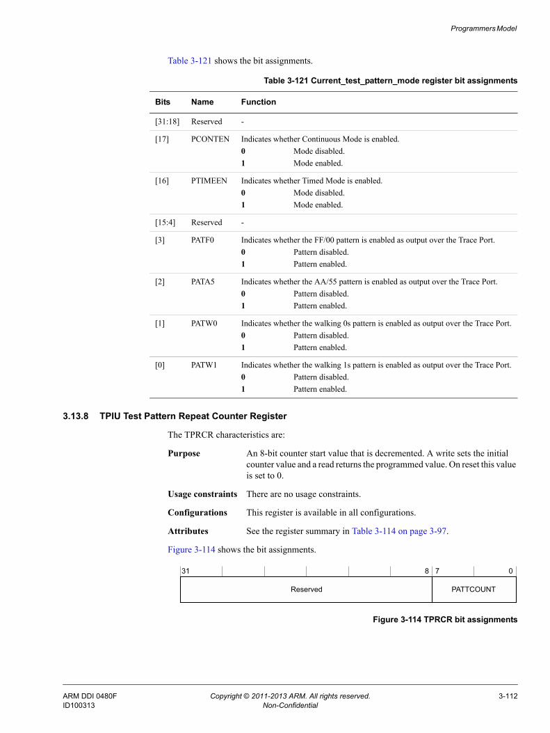
Programmers Model
Table 3-121 shows the bit assignments.
3.13.8 TPIU Test Pattern Repeat Counter Register
The TPRCR characteristics are:
Purpose An 8-bit counter start value that is decremented. A write sets the initial counter value and a read returns the programmed value. On reset this value is set to 0.
Usage constraints There are no usage constraints.
Configurations This register is available in all configurations.
Attributes See the register summary in Table 3-114 on page 3-97.
Figure 3-114 shows the bit assignments.
Figure 3-114 TPRCR bit assignments
Table 3-121 Current_test_pattern_mode register bit assignments
Bits Name Function
[31:18] Reserved -
[17] PCONTEN Indicates whether Continuous Mode is enabled.0 Mode disabled.1 Mode enabled.
[16] PTIMEEN Indicates whether Timed Mode is enabled.0 Mode disabled.1 Mode enabled.
[15:4] Reserved -
[3] PATF0 Indicates whether the FF/00 pattern is enabled as output over the Trace Port.0 Pattern disabled.1 Pattern enabled.
[2] PATA5 Indicates whether the AA/55 pattern is enabled as output over the Trace Port.0 Pattern disabled.1 Pattern enabled.
[1] PATW0 Indicates whether the walking 0s pattern is enabled as output over the Trace Port.0 Pattern disabled.1 Pattern enabled.
[0] PATW1 Indicates whether the walking 1s pattern is enabled as output over the Trace Port.0 Pattern disabled.1 Pattern enabled.
PATTCOUNT
31 8 7 0
Reserved
ARM DDI 0480F Copyright © 2011-2013 ARM. All rights reserved. 3-112ID100313 Non-Confidential

Programmers Model
Table 3-122 shows the bit assignments.
3.13.9 Formatter and Flush Status Register
The FFSR characteristics are:
Purpose Indicates the current status of the formatter and flush features available in the TPIU.
Usage constraints There are no usage constraints.
Configurations This register is available in all configurations.
Attributes See the register summary in Table 3-114 on page 3-97.
Figure 3-115 shows the bit assignments.
Figure 3-115 FFSR bit assignments
Table 3-123 shows the bit assignments.
Table 3-122 TPRCR bit assignments
Bits Name Function
[31:8] Reserved -
[7:0] PATTCOUNT 8-bit counter value to indicate the number of traceclkin cycles for which a pattern runs before it switches to the next pattern.The default value is 0.
Reserved
31 03 12
FIInProgFtStoppedTCPresent
Table 3-123 FFSR bit assignments
Bits Name Function
[31:3] Reserved -
[2] TCPresent Indicates whether the TRACECTL pin is available for use.0 TRACECTL pin not present.1 TRACECTL pin present.
[1] FtStopped The formatter has received a stop request signal and all trace data and post-amble is sent. Any additional trace data on the ATB interface is ignored and atreadys goes HIGH.0 Formatter has not stopped.1 Formatter has stopped.
[0] FlInProg Flush in progress.0 afvalids is LOW.1 afvalids is HIGH.
ARM DDI 0480F Copyright © 2011-2013 ARM. All rights reserved. 3-113ID100313 Non-Confidential

Programmers Model
3.13.10 Formatter and Flush Control Register
The FFCR characteristics are:
Purpose Controls the generation of stop, trigger, and flush events. To disable formatting and put the formatter into bypass mode, bits[1:0] must be 0. Setting both bits is the same as setting bit[1]. All three flush-generating conditions can be enabled together. However, if a second or third flush event is generated from another condition then the current flush completes before the next flush is serviced. Flush from flushin takes priority over flush from trigger, which in turn completes before a manually-activated flush. All trigger indication conditions can be enabled simultaneously although this can cause the appearance of multiple triggers if flush using trigger is also enabled. Both Stop On settings can be enabled although if Flush on Trigger is set up, none of the flushed data is stored. When the system stops, it returns atreadys and does not store the accepted data packets. This is to avoid stalling of any other devices that are connected to a trace replicator. If an event in the FFCR is required, it must be enabled before the originating event starts. Because requests from flushes and triggers can originate in an asynchronous clock domain, the exact time the component acts on the request cannot be determined during control configuration. To perform a stop on flush completion through a manually generated flush request, two write operations to the register are required: • One to enable the stop event, if it is not already enabled• One to generate the manual flush.
Note ARM recommends that you change the trace port width without enabling
continuous mode. Enabling continuous mode causes data to be sent from the trace port and modifying the port size can result in data not being aligned for power 2 port widths.
Usage constraints There are no usage constraints.
Configurations This register is available in all configurations.
Attributes See the register summary in Table 3-114 on page 3-97.
Figure 3-116 on page 3-115 shows the bit assignments.
ARM DDI 0480F Copyright © 2011-2013 ARM. All rights reserved. 3-114ID100313 Non-Confidential

Programmers Model
Figure 3-116 FFCR bit assignments
Table 3-124 shows the bit assignments.
31 14 13 12 11 10 9 8 7 6 5 4 3 2 1 0
ReservedEnFContEnFTC
FOnFIInFOnTrig
TrigInReserved
FOnMan_W
ReservedTrigFITrigEvt
StopFIStopTrig
Reserved
FOnMan_R
Table 3-124 FFCR bit assignments
Bits Name Function
[31:14] Reserved -
[13] StopTrig Stops the formatter after a trigger event is observed. Reset to disabled or 0.0 Disable stopping the formatter after a trigger event is observed.1 Enable stopping the formatter after a trigger event is observed.
[12] StopFl Forces the FIFO to drain off any part-completed packets.The reset value is 0.0 Disable stopping the formatter on return of afreadys.1 Enable stopping the formatter on return of afreadys.
[11] Reserved -
[10] TrigFl Indicates a trigger when flush completion on afreadys is returned.0 Disable trigger indication on return of afreadys.1 Enable trigger indication on return of afreadys.
[9] TrigEvt Indicates a trigger on a trigger event.0 Disable trigger indication on a trigger event.1 Enable trigger indication on a trigger event.
[8] TrigIn Indicates a trigger when trigin is asserted.0 Disable trigger indication when trigin is asserted.1 Enable trigger indication when trigin is asserted.
[7] Reserved -
[6] FOnMan_W Generates a flush. This bit is set to 1 when the flush has been serviced.The reset value is 0.0 Manual flush is not initiated.1 Manual flush is initiated.
ARM DDI 0480F Copyright © 2011-2013 ARM. All rights reserved. 3-115ID100313 Non-Confidential

Programmers Model
3.13.11 Formatter Synchronization Counter Register
The FSCR characteristics are:
Purpose Enables effective use on different sized TPAs without wasting large amounts of the storage capacity of the capture device. This counter contains the number of formatter frames since the last synchronization packet of 128 bits. It is a 12-bit counter with a maximum count value of 4096. This equates to synchronization every 65536 bytes, that is, 4096 packets x 16 bytes per packet. The default is set up for a synchronization packet every 1024 bytes, that is, every 64 formatter frames. If the formatter is configured for continuous mode, full and half-word sync frames are inserted during normal operation. Under these circumstances, the count value is the maximum number of complete frames between full synchronization packets.
[6] FOnMan_R Generates a flush. This bit is set to 0 when this flush is serviced.The reset value is 0.0 Manual flush is not initiated.1 Manual flush is initiated.
[5] FOnTrig Initiates a manual flush of data in the system when a trigger event occurs.The reset value is 0.A trigger event occurs when the trigger counter reaches 0, or, if the trigger counter is 0, when trigin is HIGH.0 Disable generation of flush when a Trigger Event occurs.1 Enable generation of flush when a Trigger Event occurs.
[4] FOnFlIn Enables the use of the flushin connection.The reset value is 0.0 Disable generation of flush using the flushin interface.1 Enable generation of flush using the flushin interface.
[3:2] Reserved -
[1] EnFCont Is embedded in trigger packets and indicates that no cycle is using sync packets.The reset value is 0.
Note This bit can only be changed when FtStopped is HIGH.
0 Continuous formatting disabled.1 Continuous formatting enabled.
[0] EnFTC Do not embed triggers into the formatted stream. Trace disable cycles and triggers are indicated by tracectl, where present.The reset value is 0.
Note This bit can be changed when FtStopped is HIGH.
0 Formatting disabled.1 Formatting enabled.
Table 3-124 FFCR bit assignments (continued)
Bits Name Function
ARM DDI 0480F Copyright © 2011-2013 ARM. All rights reserved. 3-116ID100313 Non-Confidential

Programmers Model
Usage constraints There are no usage constraints.
Configurations This register is available in all configurations.
Attributes See the register summary in Table 3-114 on page 3-97.
Figure 3-117 shows the bit assignments.
Figure 3-117 FSCR bit assignments
Table 3-125 shows the bit assignments.
3.13.12 TPIU EXCTL In Port register
The EXTCTL_In_Port register characteristics are:
Purpose Two ports can be used as a control and feedback mechanism for any serializers, pin sharing multiplexers, or other solutions that might be added to the trace output pins either for pin control or a high speed trace port solution. These ports are raw register banks that sample or export the corresponding external pins. The output register bank is set to all 0s on reset. The input registers sample the incoming signals and are therefore UNDEFINED.
Usage constraints There are no usage constraints.
Configurations This register is available in all configurations.
Attributes See the register summary in Table 3-114 on page 3-97.
Figure 3-118 shows the bit assignments.
Figure 3-118 EXTCTL_In_Port register bit assignments
Table 3-126 shows the bit assignments.
31 0
Reserved
12 11
CycCount
Table 3-125 FSCR bit assignments
Bits Name Function
[31:12] Reserved -
[11:0] CycCount 12-bit counter value. Indicates the number of complete frames between full synchronization packets. The default value is 0x40.
31 0
Reserved
8 7
EXTCTLIN
Table 3-126 EXTCTL_In_Port register bit assignments
Bits Name Function
[31:8] Reserved -
[7:0] EXTCTLIN EXTCTL inputs.
ARM DDI 0480F Copyright © 2011-2013 ARM. All rights reserved. 3-117ID100313 Non-Confidential

Programmers Model
3.13.13 TPIU EXCTL Out Port register
The EXTCTL_Out_Port register characteristics are:
Purpose Two ports can be used as a control and feedback mechanism for any serializers, pin sharing multiplexers, or other solutions that might be added to the trace output pins either for pin control or a high speed trace port solution. These ports are raw register banks that sample or export the corresponding external pins. The output register bank is set to all 0s on reset. The input registers sample the incoming signals and are therefore UNDEFINED.
Usage constraints There are no usage constraints.
Configurations This register is available in all configurations.
Attributes See the register summary in Table 3-114 on page 3-97.
Figure 3-119 shows the bit assignments.
Figure 3-119 EXTCTL_Out_Port register bit assignments
Table 3-127 shows the bit assignments.
3.13.14 Integration Test Trigger In and Flush In Acknowledge register
The ITTRFLINACK register characteristics are:
Purpose Enables control of the triginack and flushinack outputs from the TPIU.
Usage constraints There are no usage constraints.
Configurations This register is available in all configurations.
Attributes See the register summary in Table 3-114 on page 3-97.
Figure 3-120 shows the bit assignments.
Figure 3-120 ITTRFLINACK register bit assignments
31 0
Reserved
8 7
EXTCTLOUT
Table 3-127 EXTCTL_Out_Port register bit assignments
Bits Name Function
[31:8] Reserved -
[7:0] EXTCTLOUT EXTCTL outputs.
31 0
Reserved
FLUSHINACK
2 1
TRIGINACK
ARM DDI 0480F Copyright © 2011-2013 ARM. All rights reserved. 3-118ID100313 Non-Confidential

Programmers Model
Table 3-128 shows the bit assignments.
3.13.15 Integration Test Trigger In and Flush In register
The ITTRFLIN register characteristics are:
Purpose Contains the values of the flushin and trigin inputs to the TPIU.
Usage constraints There are no usage constraints.
Configurations This register is available in all configurations.
Attributes See the register summary in Table 3-114 on page 3-97.
Figure 3-121 shows the bit assignments.
Figure 3-121 ITTRFLIN register bit assignments
Table 3-129 shows the bit assignments.
Table 3-128 ITTRFLINACK register bit assignments
Bits Name Function
[31:2] Reserved -
[1] FLUSHINACK Sets the value of flushinack.0 Sets the value of flushinack to 0.1 Sets the value of flushinack to 1.
[0] TRIGINACK Sets the value of triginack.0 Sets the value of triginack to 0.1 Sets the value of triginack to 1.
31 0
Reserved
FLUSHIN
2 1
TRIGIN
Table 3-129 ITTRFLIN register bit assignments
Bits Name Function
[31:2] Reserved -
[1] FLUSHIN Reads the value of flushin.0 flushin is LOW.1 flushin is HIGH.
[0] TRIGIN Reads the value of trigin.0 trigin is LOW.1 trigin is HIGH.
ARM DDI 0480F Copyright © 2011-2013 ARM. All rights reserved. 3-119ID100313 Non-Confidential

Programmers Model
3.13.16 Integration Test ATB Data register 0
The ITATBDATA0 register characteristics are:
Purpose Contains the value of the atdatas inputs to the TPIU. The values are valid only when atvalids is HIGH.
Usage constraints There are no usage constraints.
Configurations This register is available in all configurations.
Attributes See the register summary in Table 3-114 on page 3-97.
Figure 3-122 shows the bit assignments.
Figure 3-122 ITATBDATA0 register bit assignments
Table 3-130 shows the bit assignments.
31 0
Reserved
ATDATA_0
5 4 3 2 1
ATDATA_7
ATDATA_15
ATDATA_23
ATDATA_31
Table 3-130 ITATBDATA0 register bit assignments
Bits Name Function
[31:5] Reserved -
[4] ATDATA_31 Reads the value of atdatas[31].1 atdatas[31] is 1.0 atdatas[31] is 0.
[3] ATDATA_23 Reads the value of atdatas[23].1 atdatas[23] is 1.0 atdatas[23] is 0.
[2] ATDATA_15 Reads the value of atdatas[15].1 atdatas[15] is 1.0 atdatas[15] is 0.
[1] ATDATA_7 Reads the value of atdatas[7].1 atdatas[7] is 1.0 atdatas[7] is 0.
[0] ATDATA_0 Reads the value of atdatas[0].1 atdatas[0] is 1.0 atdatas[0] is 0.
ARM DDI 0480F Copyright © 2011-2013 ARM. All rights reserved. 3-120ID100313 Non-Confidential

Programmers Model
3.13.17 Integration Test ATB Control Register 2
The ITATBCTR2 characteristics are:
Purpose Enables control of the atreadys and afvalids outputs of the TPIU.
Usage constraints There are no usage constraints.
Configurations This register is available in all configurations.
Attributes See the register summary in Table 3-114 on page 3-97.
Figure 3-123 shows the bit assignments.
Figure 3-123 ITATBCTR2 bit assignments
Table 3-131 shows the bit assignments.
3.13.18 Integration Test ATB Control Register 1
The ITATBCTR1 characteristics are:
Purpose Contains the value of the atids input to the TPIU. This is only valid when atvalids is HIGH.
Usage constraints There are no usage constraints.
Configurations This register is available in all configurations.
Attributes See the register summary in Table 3-114 on page 3-97.
Figure 3-124 shows the bit assignments.
Figure 3-124 ITATBCTR1 bit assignments
31 0
Reserved
AFVALID
2 1
ATREADY
Table 3-131 ITATBCTR2 bit assignments
Bits Name Function
[31:2] Reserved -
[1] AFVALID Sets the value of afvalid.0 Sets the value of afvalid to 0.1 Sets the value of afvalid to 1.
[0] ATREADY Sets the value of atready.0 Sets the value of atready to 0.1 Sets the value of atready to 1.
31 0
Reserved
7 6
ATID
ARM DDI 0480F Copyright © 2011-2013 ARM. All rights reserved. 3-121ID100313 Non-Confidential

Programmers Model
Table 3-132 shows the bit assignments.
3.13.19 Integration Test ATB Control Register 0
The ITATBCTR0 characteristics are:
Purpose Captures the values of the atvalids, afreadys, and atbytess inputs to the TPIU. To ensure the integration registers work correctly in a system, the value of atbytess is only valid when atvalids, bit[0], is HIGH.
Usage constraints There are no usage constraints.
Configurations This register is available in all configurations.
Attributes See the register summary in Table 3-114 on page 3-97.
Figure 3-125 shows the bit assignments.
Figure 3-125 ITATBCTR0 bit assignments
Table 3-133 shows the bit assignments.
Table 3-132 ITATBCTR1 bit assignments
Bits Name Function
[31:7] Reserved -
[6:0] ATID Reads the value of atids.
31 0
Reserved
7 2
Reserved
10 9 8 1
ATVALIDAFREADYATBYTES
Table 3-133 ITATBCTR0 bit assignments
Bits Name Function
[31:10] Reserved -
[9:8] ATBYTES Reads the value of atbytess.
[7:2] Reserved -
[1] AFREADY Reads the value of afreadys.0 afreadys is 0.1 afreadys is 1.
[0] ATVALID Reads the value of atvalids.0 atvalids is 0.1 atvalids is 1.
ARM DDI 0480F Copyright © 2011-2013 ARM. All rights reserved. 3-122ID100313 Non-Confidential
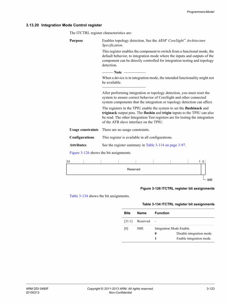
Programmers Model
3.13.20 Integration Mode Control register
The ITCTRL register characteristics are:
Purpose Enables topology detection. See the ARM® CoreSight™ Architecture Specification.This register enables the component to switch from a functional mode, the default behavior, to integration mode where the inputs and outputs of the component can be directly controlled for integration testing and topology detection.
Note When a device is in integration mode, the intended functionality might not
be available.
After performing integration or topology detection, you must reset the system to ensure correct behavior of CoreSight and other connected system components that the integration or topology detection can affect.The registers in the TPIU enable the system to set the flushinack and triginack output pins. The flushin and trigin inputs to the TPIU can also be read. The other Integration Test registers are for testing the integration of the ATB slave interface on the TPIU.
Usage constraints There are no usage constraints.
Configurations This register is available in all configurations.
Attributes See the register summary in Table 3-114 on page 3-97.
Figure 3-126 shows the bit assignments.
Figure 3-126 ITCTRL register bit assignments
Table 3-134 shows the bit assignments.
31 1 0
Reserved
IME
Table 3-134 ITCTRL register bit assignments
Bits Name Function
[31:1] Reserved -
[0] IME Integration Mode Enable. 0 Disable integration mode.1 Enable integration mode.
ARM DDI 0480F Copyright © 2011-2013 ARM. All rights reserved. 3-123ID100313 Non-Confidential

Programmers Model
3.13.21 Claim Tag Set register
The CLAIMSET register characteristics are:
Purpose Software can use the claim tag to coordinate application and debugger access to trace unit functionality. The claim tags have no effect on the operation of the component. The CLAIMSET register sets bits in the claim tag, and determines the number of claim bits implemented.
Usage constraints There are no usage constraints.
Configurations This register is available in all configurations.
Attributes See the register summary in Table 3-114 on page 3-97.
Figure 3-127 shows the bit assignments.
Figure 3-127 CLAIMSET register bit assignments
Table 3-135 shows the bit assignments.
3.13.22 Claim Tag Clear register
The CLAIMCLR register characteristics are:
Purpose Software can use the claim tag to coordinate application and debugger access to trace unit functionality. The claim tags have no effect on the operation of the component. The CLAIMCLR register sets the bits in the claim tag to 0 and determines the current value of the claim tag.
Usage constraints There are no usage constraints.
Configurations This register is available in all configurations.
Attributes See the register summary in Table 3-114 on page 3-97.
Figure 3-128 shows the bit assignments.
Figure 3-128 CLAIMCLR register bit assignments
Reserved
31 4 3 0
SET
Table 3-135 CLAIMSET register bit assignments
Bits Name Function
[31:4] Reserved -
[3:0] SET On reads, for each bit: 1 Claim tag bit is implementedOn writes, for each bit:0 Has no effect.1 Sets the relevant bit of the claim tag.
Reserved
31 4 3 0
CLR
ARM DDI 0480F Copyright © 2011-2013 ARM. All rights reserved. 3-124ID100313 Non-Confidential

Programmers Model
Table 3-136 shows the bit assignments.
3.13.23 Lock Access Register
The LAR characteristics are:
Purpose Controls write access from self-hosted, on-chip accesses. The LAR does not affect the accesses using the external debugger interface.
Usage constraints There are no usage constraints.
Configurations This register is available in all configurations.
Attributes See the register summary in Table 3-114 on page 3-97.
Figure 3-129 shows the bit assignments.
Figure 3-129 LAR bit assignments
Table 3-137 shows the bit assignments.
3.13.24 Lock Status Register
The LSR characteristics are:
Purpose Indicates the status of the lock control mechanism. This lock prevents accidental writes. When locked, write accesses are denied for all registers except for the LAR. The lock registers do not affect accesses from the external debug interface. This register reads as 0 when accessed from the external debug interface.
Usage constraints There are no usage constraints.
Table 3-136 CLAIMCLR register bit assignments
Bits Name Function
[31:4] Reserved -
[3:0] CLR On reads, for each bit: 0 Claim tag bit is not set.1 Claim tag bit is set.On writes, for each bit: 0 Has no effect.1 Clears the relevant bit of the claim tag.
31 0
KEY
Table 3-137 LAR bit assignments
Bits Name Function
[31:0] KEY Software lock key value. 0xC5ACCE55 Clear the software lock.All other write values set the software lock.
ARM DDI 0480F Copyright © 2011-2013 ARM. All rights reserved. 3-125ID100313 Non-Confidential

Programmers Model
Configurations This register is available in all configurations.
Attributes See the register summary in Table 3-114 on page 3-97.
Figure 3-130 shows the bit assignments.
Figure 3-130 LSR bit assignments
Table 3-138 shows the bit assignments.
3.13.25 Authentication Status register
The AUTHSTATUS register characteristics are:
Purpose Reports the required security level and present status.
Usage constraints There are no usage constraints.
Configurations This register is available in all configurations.
Attributes See the register summary in Table 3-114 on page 3-97.
Figure 3-131 shows the bit assignments.
Figure 3-131 AUTHSTATUS register bit assignments
Reserved
31 03 12
SLISLKnTT
Table 3-138 LSR bit assignments
Bits Name Function
[31:3] Reserved -
[2] nTT Register size indicator. Always 0. Indicates that the LAR is implemented as 32-bit.
[1] SLK Software Lock Status. Returns the present lock status of the device, from the current interface.0 Indicates that write operations are permitted from this interface.1 Indicates that write operations are not permitted from this interface. Read operations are
permitted.
[0] SLI Software Lock Implemented. Indicates that a lock control mechanism is present from this interface.0 Indicates that a lock control mechanism is not present from this interface. Write operations to
the LAR are ignored.1 Indicates that a lock control mechanism is present from this interface.
31 8 7 6 5 4 3 2 0
Reserved
NSIDNSNIDSIDSNID
1
ARM DDI 0480F Copyright © 2011-2013 ARM. All rights reserved. 3-126ID100313 Non-Confidential

Programmers Model
Table 3-139 shows the bit assignments.
3.13.26 Device Configuration register
The DEVID register characteristics are:
Purpose Indicates the capabilities of the component.
Usage constraints There are no usage constraints.
Configurations This register is available in all configurations.
Attributes See the register summary in Table 3-114 on page 3-97.
Figure 3-132 shows the bit assignments.
Figure 3-132 DEVID register bit assignments
Table 3-140 shows the bit assignments.
Table 3-139 AUTHSTATUS register bit assignments
Bits Name Function
[31:8] Reserved -
[7:6] SNID Indicates the security level for secure non-invasive debug:0b00 Functionality is not implemented or is controlled elsewhere.
[5:4] SID Indicates the security level for secure invasive debug:0b00 Functionality is not implemented or is controlled elsewhere.
[3:2] NSNID Indicates the security level for non-secure non-invasive debug:0b00 Functionality is not implemented or is controlled elsewhere.
[1:0] NSID Indicates the security level for non-secure invasive debug:0b00 Functionality is not implemented or is controlled elsewhere.
31 12 11 10 9 8 6 5 4 0
FIFOSIZECLKRELAT
MUXNUM
TCLKDATASWOMANSWOUARTNRZ
Reserved
Table 3-140 DEVID register bit assignments
Bits Name Function
[31:12] Reserved -
[11] SWOUARTNRZ Indicates whether Serial Wire Output, UART or NRZ, is supported.0 Serial Wire Output, UART or NRZ, is not supported.
[10] SWOMAN Indicates whether Serial Wire Output, Manchester encoded format, is supported. 0 Serial Wire Output, Manchester encoded format, is not supported.
ARM DDI 0480F Copyright © 2011-2013 ARM. All rights reserved. 3-127ID100313 Non-Confidential

Programmers Model
3.13.27 Device Type Identifier register
The DEVTYPE register characteristics are:
Purpose Provides a debugger with information about the component when the Part Number field is not recognized. The debugger can then report this information.
Usage constraints There are no usage constraints.
Configurations This register is available in all configurations.
Attributes See the register summary in Table 3-114 on page 3-97.
Figure 3-133 shows the bit assignments.
Figure 3-133 DEVTYPE register bit assignments
Table 3-141 shows the bit assignments.
[9] TCLKDATA Indicates whether trace clock plus data is supported.0 Trace clock and data is supported.
[8:6] FIFOSIZE FIFO size in powers of 2.0b010 FIFO size of 4 entries, that is, 16 bytes.
[5] CLKRELAT Indicates the relationship between atclk and traceclkin.1 atclk and traceclkin are asynchronous.
[4:0] MUXNUM Indicates the hidden level of input multiplexing. When non-zero, this value indicates the type of multiplexing on the input to the ATB. Currently only 0x00 is supported, that is, no multiplexing is present. This value helps detect the ATB structure.
Table 3-140 DEVID register bit assignments (continued)
Bits Name Function
31 0
Reserved
7
SUB
8 4
MAJOR
3
Table 3-141 DEVTYPE register bit assignments
Bits Name Function
[31:8] Reserved -
[7:4] SUB Sub-classification of the type of the debug component as specified in the ARM® CoreSight™ Architecture Specification within the major classification as specified in the MAJOR field.0b0001 Indicates that this component is a trace port component.
[3:0] MAJOR Major classification of the type of the debug component as specified in the ARM® CoreSight™ Architecture Specification for this debug and trace component.0b0001 Indicates that this component is a trace sink component.
ARM DDI 0480F Copyright © 2011-2013 ARM. All rights reserved. 3-128ID100313 Non-Confidential

Programmers Model
3.13.28 Peripheral ID4 Register
The PIDR4 characteristics are:
Purpose Part of the set of peripheral identification registers. Contains part of the designer identity and the memory size.
Usage constraints There are no usage constraints.
Configurations This register is available in all configurations.
Attributes See the register summary in Table 3-114 on page 3-97.
Figure 3-134 shows the bit assignments.
Figure 3-134 PIDR4 bit assignments
Table 3-142 shows the bit assignments.
3.13.29 Peripheral ID0 Register
The PIDR0 characteristics are:
Purpose Part of the set of peripheral identification registers. Contains part of the designer-specific part number.
Usage constraints There are no usage constraints.
Configurations This register is available in all configurations.
Attributes See the register summary in Table 3-114 on page 3-97.
Figure 3-135 shows the bit assignments.
Figure 3-135 PIDR0 bit assignments
31 0
Reserved
7
SIZE
8 4
DES_2
3
Table 3-142 PIDR4 bit assignments
Bits Name Function
[31:8] Reserved -
[7:4] SIZE Always 0b0000. Indicates that the device only occupies 4KB of memory.
[3:0] DES_2 Together, PIDR1.DES_0, PIDR2.DES_1, and PIDR4.DES_2 identify the designer of the component.0b0100 JEDEC continuation code.
31 0
Reserved
78
PART_0
ARM DDI 0480F Copyright © 2011-2013 ARM. All rights reserved. 3-129ID100313 Non-Confidential

Programmers Model
Table 3-143 shows the bit assignments.
3.13.30 Peripheral ID1 Register
The PIDR1 characteristics are:
Purpose Part of the set of peripheral identification registers. Contains part of the designer-specific part number and part of the designer identity.
Usage constraints There are no usage constraints.
Configurations This register is available in all configurations.
Attributes See the register summary in Table 3-114 on page 3-97.
Figure 3-136 shows the bit assignments.
Figure 3-136 PIDR1 bit assignments
Table 3-144 shows the bit assignments.
3.13.31 Peripheral ID2 Register
The PIDR2 characteristics are:
Purpose Part of the set of peripheral identification registers. Contains part of the designer identity and the product revision.
Usage constraints There are no usage constraints.
Configurations This register is available in all configurations.
Table 3-143 PIDR0 bit assignments
Bits Name Function
[31:8] Reserved -
[7:0] PART_0 Bits[7:0] of the 12-bit part number of the component. The designer of the component assigns this part number.0x12 Indicates bits[7:0] of the part number of the component.
31 0
Reserved
78
PART_1
4 3
DES_0
Table 3-144 PIDR1 bit assignments
Bits Name Function
[31:8] Reserved -
[7:4] DES_0 Together, PIDR1.DES_0, PIDR2.DES_1, and PIDR4.DES_2 identify the designer of the component.0b1011 ARM. Bits[3:0] of the JEDEC JEP106 Identity Code.
[3:0] PART_1 Bits[11:8] of the 12-bit part number of the component. The designer of the component assigns this part number.0b1001 Indicates bits[11:8] of the part number of the component.
ARM DDI 0480F Copyright © 2011-2013 ARM. All rights reserved. 3-130ID100313 Non-Confidential

Programmers Model
Attributes See the register summary in Table 3-114 on page 3-97.
Figure 3-137 shows the bit assignments.
Figure 3-137 PIDR2 bit assignments
Table 3-145 shows the bit assignments.
3.13.32 Peripheral ID3 Register
The PIDR3 characteristics are:
Purpose Part of the set of peripheral identification registers. Contains the REVAND and CMOD fields.
Usage constraints There are no usage constraints.
Configurations This register is available in all configurations.
Attributes See the register summary in Table 3-114 on page 3-97.
Figure 3-138 shows the bit assignments.
Figure 3-138 PIDR3 bit assignments
31 0
Reserved
7
REVISION
8 4
DES_1
3 2
JEDEC
Table 3-145 PIDR2 bit assignments
Bits Name Function
[31:8] Reserved -
[7:4] REVISION 0b0100 This device is at r0p5.
[3] JEDEC Always 1. Indicates that the JEDEC-assigned designer ID is used.
[2:0] DES_1 Together, PIDR1.DES_0, PIDR2.DES_1, and PIDR4.DES_2 identify the designer of the component.0b011 ARM. Bits[6:4] of the JEDEC JEP106 Identity Code.
31 0
Reserved
7
REVAND
8 4
CMOD
3
ARM DDI 0480F Copyright © 2011-2013 ARM. All rights reserved. 3-131ID100313 Non-Confidential

Programmers Model
Table 3-146 shows the bit assignments.
3.13.33 Component ID0 Register
The CIDR0 characteristics are:
Purpose A component identification register that indicates the presence of identification registers.
Usage constraints There are no usage constraints.
Configurations This register is available in all configurations.
Attributes See the register summary in Table 3-114 on page 3-97.
Figure 3-139 shows the bit assignments.
Figure 3-139 CIDR0 bit assignments
Table 3-147 shows the bit assignments.
3.13.34 Component ID1 Register
The CIDR1 characteristics are:
Purpose A component identification register that indicates the presence of identification registers. This register also indicates the component class.
Usage constraints There are no usage constraints.
Configurations This register is available in all configurations.
Attributes See the register summary in Table 3-114 on page 3-97.
Figure 3-140 on page 3-133 shows the bit assignments.
Table 3-146 PIDR3 bit assignments
Bits Name Function
[31:8] Reserved -
[7:4] REVAND 0b0000 Indicates that there are no errata fixes to this component.
[3:0] CMOD Customer Modified. Indicates whether the customer has modified the behavior of the component. In most cases, this field is 0b0000. Customers change this value when they make authorized modifications to this component.0b0000 Indicates that the customer has not modified this component.
PRMBL_0
31 8 7 0
Reserved
Table 3-147 CIDR0 bit assignments
Bits Name Function
[31:8] Reserved -
[7:0] PRMBL_0 Preamble[0]. Contains bits[7:0] of the component identification code.0x0D Bits[7:0] of the identification code.
ARM DDI 0480F Copyright © 2011-2013 ARM. All rights reserved. 3-132ID100313 Non-Confidential

Programmers Model
Figure 3-140 CIDR1 bit assignments
Table 3-148 shows the bit assignments.
3.13.35 Component ID2 Register
The CIDR2 characteristics are:
Purpose A component identification register that indicates that the presence of identification registers.
Usage constraints There are no usage constraints.
Configurations This register is available in all configurations.
Attributes See the register summary in Table 3-114 on page 3-97.
Figure 3-141 shows the bit assignments.
Figure 3-141 CIDR2 bit assignments
Table 3-149 shows the bit assignments.
3.13.36 Component ID3 Register
The CIDR3 characteristics are:
Purpose A component identification register that indicates the presence of identification registers.
31 8 7 4 3 0
PRMBL_1CLASSReserved
Table 3-148 CIDR1 bit assignments
Bits Name Function
[31:8] Reserved -
[7:4] CLASS Class of the component, for example, whether the component is a ROM table or a generic CoreSight SoC-400 component. Contains bits[15:12] of the component identification code.0b1001 Indicates that the component is a CoreSight SoC-400 component.
[3:0] PRMBL_1 Preamble[1]. Contains bits[11:8] of the component identification code.0b0000 Bits[11:8] of the identification code.
PRMBL_2
31 8 7 0
Reserved
Table 3-149 CIDR2 bit assignments
Bits Name Function
[31:8] Reserved -
[7:0] PRMBL_2 Preamble[2]. Contains bits[23:16] of the component identification code.0x05 Bits[23:16] of the identification code.
ARM DDI 0480F Copyright © 2011-2013 ARM. All rights reserved. 3-133ID100313 Non-Confidential

Programmers Model
Usage constraints There are no usage constraints.
Configurations This register is available in all configurations.
Attributes See the register summary in Table 3-114 on page 3-97.
Figure 3-142 shows the bit assignments.
Figure 3-142 CIDR3 bit assignments
Table 3-150 shows the bit assignments.
31 0
Reserved
78
PRMBL_3
Table 3-150 CIDR3 bit assignments
Bits Name Function
[31:8] Reserved -
[7:0] PRMBL_3 Preamble[3]. Contains bits[31:24] of the component identification code.0xB1 Bits[31:24] of the identification code.
ARM DDI 0480F Copyright © 2011-2013 ARM. All rights reserved. 3-134ID100313 Non-Confidential

Programmers Model
3.14 CTI register summaryTable 3-151 shows the CTI registers in offset order from the base memory address.
Table 3-151 CTI register summary
Offset Name Type Reset Description
0x000 CTICONTROL RW 0x00000000 CTI Control register on page 3-137
0x010 CTIINTACK WO 0x00000000 CTI Interrupt Acknowledge register on page 3-137
0x014 CTIAPPSET RW 0x00000000 CTI Application Trigger Set register on page 3-138
0x018 CTIAPPCLEAR WO 0x00000000 CTI Application Trigger Clear register on page 3-138
0x01C CTIAPPPULSE WO 0x00000000 CTI Application Pulse register on page 3-139
0x020 CTIINEN0 RW 0x00000000 CTI Trigger 0 to Channel Enable register on page 3-140
0x024 CTIINEN1 RW 0x00000000 CTI Trigger 1 to Channel Enable register on page 3-140
0x028 CTIINEN2 RW 0x00000000 CTI Trigger 2 to Channel Enable register on page 3-141
0x02C CTIINEN3 RW 0x00000000 CTI Trigger 3 to Channel Enable register on page 3-142
0x030 CTIINEN4 RW 0x00000000 CTI Trigger 4 to Channel Enable register on page 3-143
0x034 CTIINEN5 RW 0x00000000 CTI Trigger 5 to Channel Enable register on page 3-143
0x038 CTIINEN6 RW 0x00000000 CTI Trigger 6 to Channel Enable register on page 3-144
0x03C CTIINEN7 RW 0x00000000 CTI Trigger 7 to Channel Enable register on page 3-145
0x0A0 CTIOUTEN0 RW 0x00000000 CTI Channel to Trigger 0 Enable register on page 3-145
0x0A4 CTIOUTEN1 RW 0x00000000 CTI Channel to Trigger 1 Enable register on page 3-146
0x0A8 CTIOUTEN2 RW 0x00000000 CTI Channel to Trigger 2 Enable register on page 3-147
0x0AC CTIOUTEN3 RW 0x00000000 CTI Channel to Trigger 3 Enable register on page 3-147
0x0B0 CTIOUTEN4 RW 0x00000000 CTI Channel to Trigger 4 Enable register on page 3-148
0x0B4 CTIOUTEN5 RW 0x00000000 CTI Channel to Trigger 5 Enable register on page 3-148
0x0B8 CTIOUTEN6 RW 0x00000000 CTI Channel to Trigger 6 Enable register on page 3-149
0x0BC CTIOUTEN7 RW 0x00000000 CTI Channel to Trigger 7 Enable register on page 3-150
0x130 CTITRIGINSTATUS RO 0x00000000 CTI Trigger In Status register on page 3-150
0x134 CTITRIGOUTSTATUS RO 0x00000000 CTI Trigger Out Status register on page 3-151
0x138 CTICHINSTATUS RO 0x00000000 CTI Channel In Status register on page 3-152
0x13C CTICHOUTSTATUS RO 0x00000000 CTI Channel Out Status register on page 3-152
0x140 CTIGATE RW 0x0000000F Enable CTI Channel Gate register on page 3-153
0x144 asicctl RW 0x00000000 External Multiplexer Control register on page 3-154
0xEDC ITCHINACK WO 0x00000000 Integration Test Channel Input Acknowledge register on page 3-154
0xEE0 ITTRIGINACK WO 0x00000000 Integration Test Trigger Input Acknowledge register on page 3-155
0xEE4 ITCHOUT WO 0x00000000 Integration Test Channel Output register on page 3-155
ARM DDI 0480F Copyright © 2011-2013 ARM. All rights reserved. 3-135ID100313 Non-Confidential
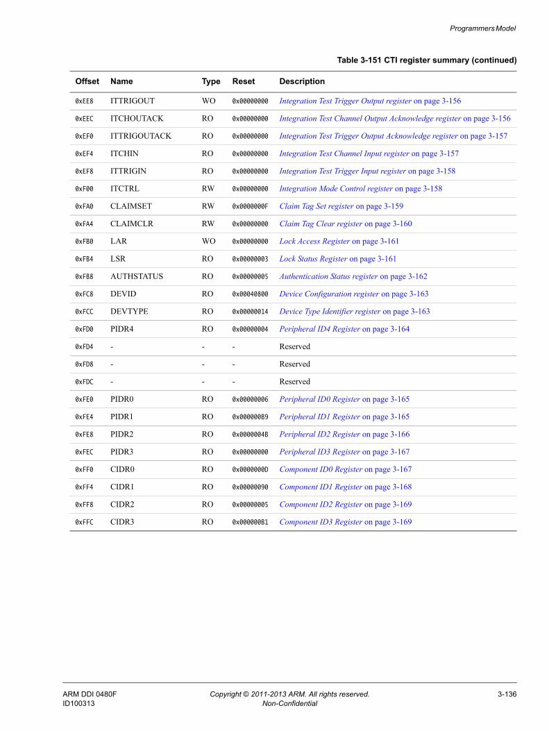
Programmers Model
0xEE8 ITTRIGOUT WO 0x00000000 Integration Test Trigger Output register on page 3-156
0xEEC ITCHOUTACK RO 0x00000000 Integration Test Channel Output Acknowledge register on page 3-156
0xEF0 ITTRIGOUTACK RO 0x00000000 Integration Test Trigger Output Acknowledge register on page 3-157
0xEF4 ITCHIN RO 0x00000000 Integration Test Channel Input register on page 3-157
0xEF8 ITTRIGIN RO 0x00000000 Integration Test Trigger Input register on page 3-158
0xF00 ITCTRL RW 0x00000000 Integration Mode Control register on page 3-158
0xFA0 CLAIMSET RW 0x0000000F Claim Tag Set register on page 3-159
0xFA4 CLAIMCLR RW 0x00000000 Claim Tag Clear register on page 3-160
0xFB0 LAR WO 0x00000000 Lock Access Register on page 3-161
0xFB4 LSR RO 0x00000003 Lock Status Register on page 3-161
0xFB8 AUTHSTATUS RO 0x00000005 Authentication Status register on page 3-162
0xFC8 DEVID RO 0x00040800 Device Configuration register on page 3-163
0xFCC DEVTYPE RO 0x00000014 Device Type Identifier register on page 3-163
0xFD0 PIDR4 RO 0x00000004 Peripheral ID4 Register on page 3-164
0xFD4 - - - Reserved
0xFD8 - - - Reserved
0xFDC - - - Reserved
0xFE0 PIDR0 RO 0x00000006 Peripheral ID0 Register on page 3-165
0xFE4 PIDR1 RO 0x000000B9 Peripheral ID1 Register on page 3-165
0xFE8 PIDR2 RO 0x0000004B Peripheral ID2 Register on page 3-166
0xFEC PIDR3 RO 0x00000000 Peripheral ID3 Register on page 3-167
0xFF0 CIDR0 RO 0x0000000D Component ID0 Register on page 3-167
0xFF4 CIDR1 RO 0x00000090 Component ID1 Register on page 3-168
0xFF8 CIDR2 RO 0x00000005 Component ID2 Register on page 3-169
0xFFC CIDR3 RO 0x000000B1 Component ID3 Register on page 3-169
Table 3-151 CTI register summary (continued)
Offset Name Type Reset Description
ARM DDI 0480F Copyright © 2011-2013 ARM. All rights reserved. 3-136ID100313 Non-Confidential

Programmers Model
3.15 CTI register descriptionsThis section describes the CTI registers. Table 3-151 on page 3-135 provides cross-references to individual registers.
3.15.1 CTI Control register
The CTICONTROL register characteristics are:
Purpose Enables the CTI.
Usage constraints There are no usage constraints.
Configurations This register is available in all configurations.
Attributes See the register summary in Table 3-151 on page 3-135.
Figure 3-143 shows the bit assignments.
Figure 3-143 CTICONTROL register bit assignments
Table 3-152 shows the bit assignments.
3.15.2 CTI Interrupt Acknowledge register
The CTIINTACK register characteristics are:
Purpose Software acknowledge for a trigger output. This register is used when ctitrigout is used as a sticky output. That is, no hardware acknowledge is available and software acknowledge is required.
Usage constraints There are no usage constraints.
Configurations This register is available in all configurations.
Attributes See the register summary in Table 3-151 on page 3-135.
Figure 3-144 shows the bit assignments.
Figure 3-144 CTIINTACK register bit assignments
31 1 0
Reserved
GLBEN
Table 3-152 CTICONTROL register bit assignments
Bits Name Function
[31:1] Reserved -
[0] GLBEN Enables or disables the CTI.0 When this bit is 0, all cross-triggering mapping logic functionality is disabled.1 When this bit is 1, cross-triggering mapping logic functionality is enabled.
31 0
Reserved
78
INTACK
ARM DDI 0480F Copyright © 2011-2013 ARM. All rights reserved. 3-137ID100313 Non-Confidential

Programmers Model
Table 3-153 shows the bit assignments.
3.15.3 CTI Application Trigger Set register
The CTIAPPSET register characteristics are:
Purpose A write to this register causes a channel event to be raised, corresponding to the bit written to.
Usage constraints There are no usage constraints.
Configurations This register is available in all configurations.
Attributes See the register summary in Table 3-151 on page 3-135.
Figure 3-145 shows the bit assignments.
Figure 3-145 CTIAPPSET register bit assignments
Table 3-154 shows the bit assignments.
3.15.4 CTI Application Trigger Clear register
The CTIAPPCLEAR register characteristics are:
Purpose Writing to a bit in this register clears the corresponding channel event.
Usage constraints There are no usage constraints.
Configurations This register is available in all configurations.
Table 3-153 CTIINTACK register bit assignments
Bits Name Function
[31:8] Reserved -
[7:0] INTACK Acknowledges the corresponding ctitrigout output. There is one bit of the register for each ctitrigout output. When a 1 is written to a bit in this register, the corresponding ctitrigout is acknowledged, causing it to be cleared.
31 0
Reserved
34
APPSET
Table 3-154 CTIAPPSET register bit assignments
Bits Name Function
[31:4] Reserved -
[3:0] APPSET Setting a bit HIGH generates a channel event for the selected channel. There is one bit of the register for each channel. Reads as follows: 0 Application trigger is inactive.1 Application trigger is active.Writes as follows: 0 No effect.1 Generate channel event.
ARM DDI 0480F Copyright © 2011-2013 ARM. All rights reserved. 3-138ID100313 Non-Confidential
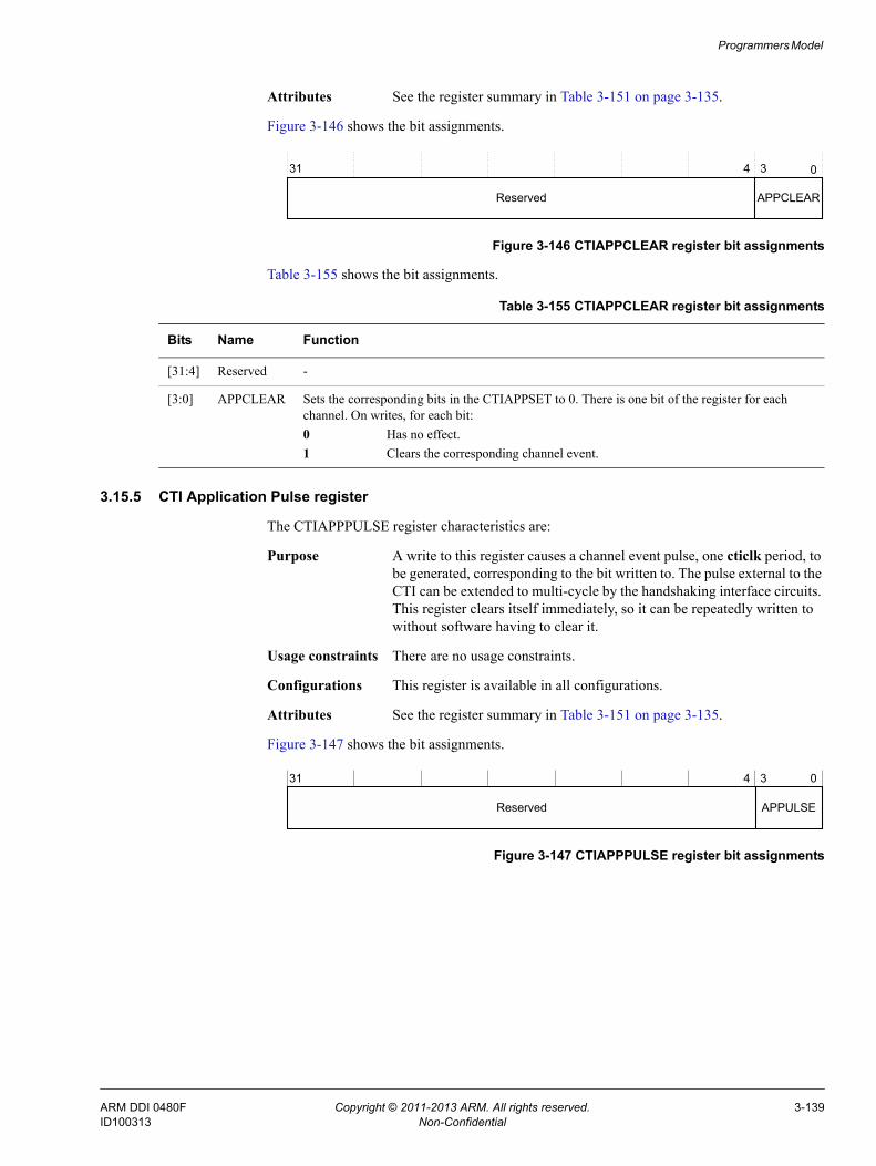
Programmers Model
Attributes See the register summary in Table 3-151 on page 3-135.
Figure 3-146 shows the bit assignments.
Figure 3-146 CTIAPPCLEAR register bit assignments
Table 3-155 shows the bit assignments.
3.15.5 CTI Application Pulse register
The CTIAPPPULSE register characteristics are:
Purpose A write to this register causes a channel event pulse, one cticlk period, to be generated, corresponding to the bit written to. The pulse external to the CTI can be extended to multi-cycle by the handshaking interface circuits. This register clears itself immediately, so it can be repeatedly written to without software having to clear it.
Usage constraints There are no usage constraints.
Configurations This register is available in all configurations.
Attributes See the register summary in Table 3-151 on page 3-135.
Figure 3-147 shows the bit assignments.
Figure 3-147 CTIAPPPULSE register bit assignments
31 0
Reserved
4
APPCLEAR
3
Table 3-155 CTIAPPCLEAR register bit assignments
Bits Name Function
[31:4] Reserved -
[3:0] APPCLEAR Sets the corresponding bits in the CTIAPPSET to 0. There is one bit of the register for each channel. On writes, for each bit: 0 Has no effect.1 Clears the corresponding channel event.
APPULSE
31 4 3 0
Reserved
ARM DDI 0480F Copyright © 2011-2013 ARM. All rights reserved. 3-139ID100313 Non-Confidential
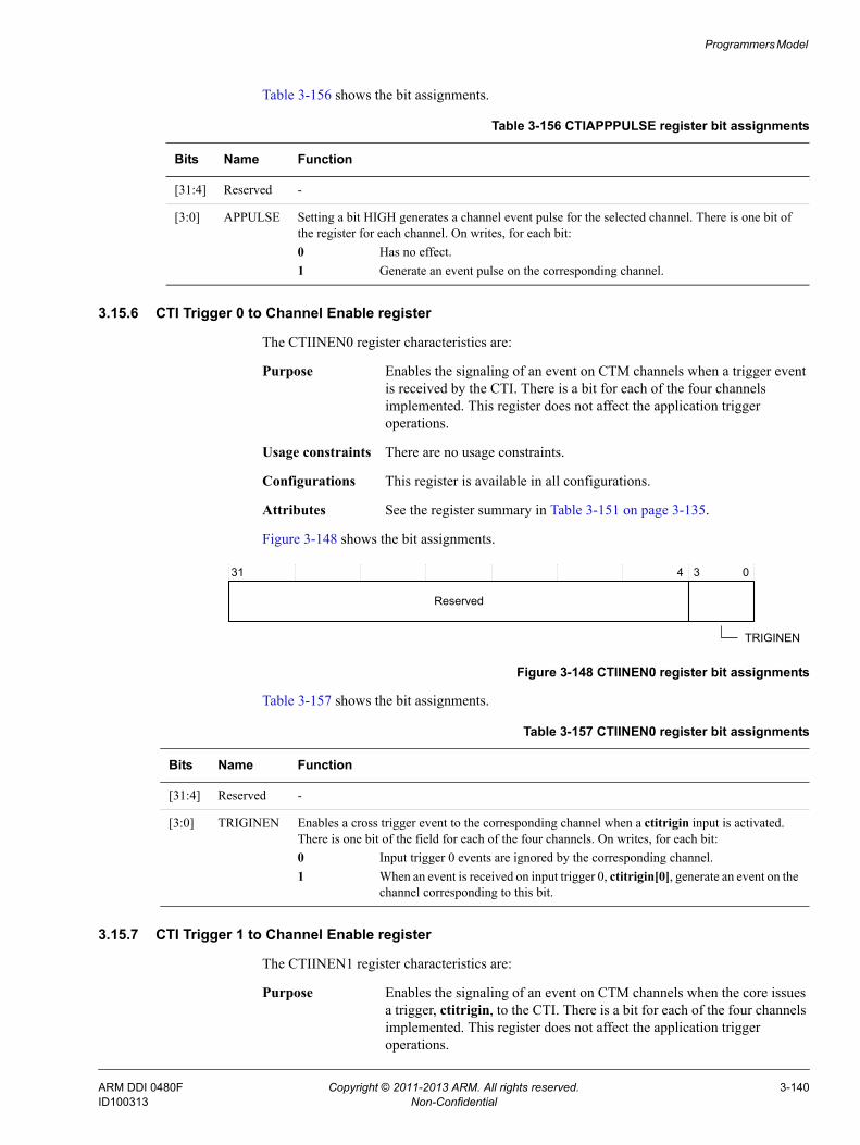
Programmers Model
Table 3-156 shows the bit assignments.
3.15.6 CTI Trigger 0 to Channel Enable register
The CTIINEN0 register characteristics are:
Purpose Enables the signaling of an event on CTM channels when a trigger event is received by the CTI. There is a bit for each of the four channels implemented. This register does not affect the application trigger operations.
Usage constraints There are no usage constraints.
Configurations This register is available in all configurations.
Attributes See the register summary in Table 3-151 on page 3-135.
Figure 3-148 shows the bit assignments.
Figure 3-148 CTIINEN0 register bit assignments
Table 3-157 shows the bit assignments.
3.15.7 CTI Trigger 1 to Channel Enable register
The CTIINEN1 register characteristics are:
Purpose Enables the signaling of an event on CTM channels when the core issues a trigger, ctitrigin, to the CTI. There is a bit for each of the four channels implemented. This register does not affect the application trigger operations.
Table 3-156 CTIAPPPULSE register bit assignments
Bits Name Function
[31:4] Reserved -
[3:0] APPULSE Setting a bit HIGH generates a channel event pulse for the selected channel. There is one bit of the register for each channel. On writes, for each bit:0 Has no effect.1 Generate an event pulse on the corresponding channel.
31 4 3 0
TRIGINEN
Reserved
Table 3-157 CTIINEN0 register bit assignments
Bits Name Function
[31:4] Reserved -
[3:0] TRIGINEN Enables a cross trigger event to the corresponding channel when a ctitrigin input is activated. There is one bit of the field for each of the four channels. On writes, for each bit: 0 Input trigger 0 events are ignored by the corresponding channel.1 When an event is received on input trigger 0, ctitrigin[0], generate an event on the
channel corresponding to this bit.
ARM DDI 0480F Copyright © 2011-2013 ARM. All rights reserved. 3-140ID100313 Non-Confidential

Programmers Model
Usage constraints There are no usage constraints.
Configurations This register is available in all configurations.
Attributes See the register summary in Table 3-151 on page 3-135.
Figure 3-149 shows the bit assignments.
Figure 3-149 CTIINEN1 register bit assignments
Table 3-158 shows the bit assignments.
3.15.8 CTI Trigger 2 to Channel Enable register
The CTIINEN2 register characteristics are:
Purpose Enables the signaling of an event on CTM channels when the core issues a trigger, ctitrigin, to the CTI. There is a bit for each of the four channels implemented. This register does not affect the application trigger operations.
Usage constraints There are no usage constraints.
Configurations This register is available in all configurations.
Attributes See the register summary in Table 3-151 on page 3-135.
Figure 3-150 shows the assignments.
Figure 3-150 CTIINEN2 register bit assignments
31 4 3 0
TRIGINEN
Reserved
Table 3-158 CTIINEN1 register bit assignments
Bits Name Function
[31:4] Reserved -
[3:0] TRIGINEN Enables a cross trigger event to the corresponding channel when a ctitrigin input is activated. There is one bit of the field for each of the four channels. On writes, for each bit: 0 Input trigger 1 events are ignored by the corresponding channel.1 When an event is received on input trigger 1, ctitrigin[1], generate an event on the
channel corresponding to this bit.
31 4 3 0
TRIGINEN
Reserved
ARM DDI 0480F Copyright © 2011-2013 ARM. All rights reserved. 3-141ID100313 Non-Confidential

Programmers Model
Table 3-159 shows the bit assignments.
3.15.9 CTI Trigger 3 to Channel Enable register
The CTIINEN3 register characteristics are:
Purpose Enables the signaling of an event on CTM channels when the core issues a trigger, ctitrigin, to the CTI. There is a bit for each of the four channels implemented. This register does not affect the application trigger operations.
Usage constraints There are no usage constraints.
Configurations This register is available in all configurations.
Attributes See the register summary in Table 3-151 on page 3-135.
Figure 3-151 shows the bit assignments.
Figure 3-151 CTIINEN3 register bit assignments
Table 3-160 shows the bit assignments.
Table 3-159 CTIINEN2 register bit assignments
Bits Name Function
[31:4] Reserved -
[3:0] TRIGINEN Enables a cross trigger event to the corresponding channel when a ctitrigin input is activated. There is one bit of the field for each of the four channels. On writes, for each bit: 0 Input trigger 2 events are ignored by the corresponding channel.1 When an event is received on input trigger 2, ctitrigin[2], generate an event on the
channel corresponding to this bit.
31 4 3 0
TRIGINEN
Reserved
Table 3-160 CTIINEN3 register bit assignments
Bits Name Function
[31:4] Reserved -
[3:0] TRIGINEN Enables a cross trigger event to the corresponding channel when a ctitrigin input is activated. There is one bit of the field for each of the four channels. On writes, for each bit: 0 Input trigger 3 events are ignored by the corresponding channel.1 When an event is received on input trigger 3, ctitrigin[3], generate an event on the
channel corresponding to this bit.
ARM DDI 0480F Copyright © 2011-2013 ARM. All rights reserved. 3-142ID100313 Non-Confidential
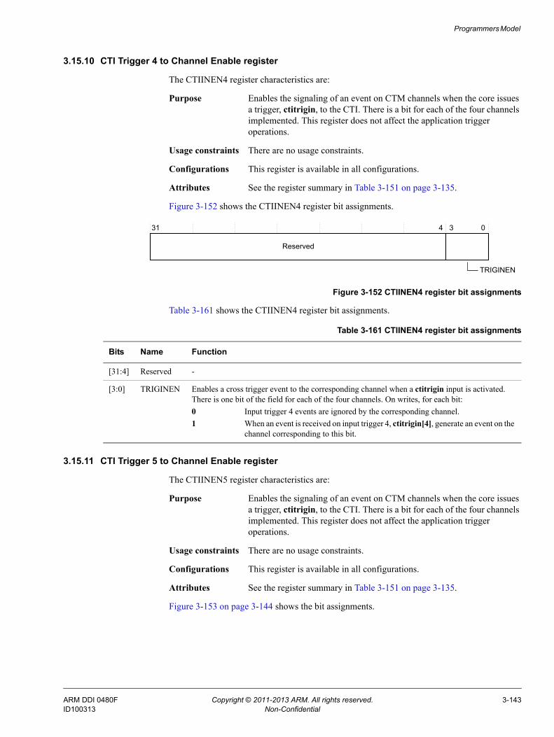
Programmers Model
3.15.10 CTI Trigger 4 to Channel Enable register
The CTIINEN4 register characteristics are:
Purpose Enables the signaling of an event on CTM channels when the core issues a trigger, ctitrigin, to the CTI. There is a bit for each of the four channels implemented. This register does not affect the application trigger operations.
Usage constraints There are no usage constraints.
Configurations This register is available in all configurations.
Attributes See the register summary in Table 3-151 on page 3-135.
Figure 3-152 shows the CTIINEN4 register bit assignments.
Figure 3-152 CTIINEN4 register bit assignments
Table 3-161 shows the CTIINEN4 register bit assignments.
3.15.11 CTI Trigger 5 to Channel Enable register
The CTIINEN5 register characteristics are:
Purpose Enables the signaling of an event on CTM channels when the core issues a trigger, ctitrigin, to the CTI. There is a bit for each of the four channels implemented. This register does not affect the application trigger operations.
Usage constraints There are no usage constraints.
Configurations This register is available in all configurations.
Attributes See the register summary in Table 3-151 on page 3-135.
Figure 3-153 on page 3-144 shows the bit assignments.
31 4 3 0
TRIGINEN
Reserved
Table 3-161 CTIINEN4 register bit assignments
Bits Name Function
[31:4] Reserved -
[3:0] TRIGINEN Enables a cross trigger event to the corresponding channel when a ctitrigin input is activated. There is one bit of the field for each of the four channels. On writes, for each bit: 0 Input trigger 4 events are ignored by the corresponding channel.1 When an event is received on input trigger 4, ctitrigin[4], generate an event on the
channel corresponding to this bit.
ARM DDI 0480F Copyright © 2011-2013 ARM. All rights reserved. 3-143ID100313 Non-Confidential

Programmers Model
Figure 3-153 CTIINEN5 register bit assignments
Table 3-162 shows the bit assignments.
3.15.12 CTI Trigger 6 to Channel Enable register
The CTIINEN6 register characteristics are:
Purpose This register does not affect the application trigger operations.
Usage constraints There are no usage constraints.
Configurations This register is available in all configurations.
Attributes See the register summary in Table 3-151 on page 3-135.
Figure 3-154 shows the bit assignments.
Figure 3-154 CTIINEN6 register bit assignments
Table 3-163 shows the bit assignments.
31 4 3 0
TRIGINEN
Reserved
Table 3-162 CTIINEN5 register bit assignments
Bits Name Function
[31:4] Reserved -
[3:0] TRIGINEN Enables a cross trigger event to the corresponding channel when a ctitrigin input is activated. There is one bit of the field for each of the four channels. On writes, for each bit: 0 Input trigger 5 events are ignored by the corresponding channel.1 When an event is received on input trigger 5, ctitrigin[5], generate an event on the
channel corresponding to this bit.
31 4 3 0
TRIGINEN
Reserved
Table 3-163 CTIINEN6 register bit assignments
Bits Name Function
[31:4] Reserved -
[3:0] TRIGINEN Enables a cross trigger event to the corresponding channel when a ctitrigin input is activated. There is one bit of the field for each of the four channels. On writes, for each bit: 0 Input trigger 6 events are ignored by the corresponding channel.1 When an event is received on input trigger 6, ctitrigin[60], generate an event on
the channel corresponding to this bit.
ARM DDI 0480F Copyright © 2011-2013 ARM. All rights reserved. 3-144ID100313 Non-Confidential

Programmers Model
3.15.13 CTI Trigger 7 to Channel Enable register
The CTIINEN7 register characteristics are:
Purpose Enables the signaling of an event on CTM channels when the core issues a trigger, ctitrigin, to the CTI. There is a bit for each of the four channels implemented. This register does not affect the application trigger operations.
Usage constraints There are no usage constraints.
Configurations This register is available in all configurations.
Attributes See the register summary in Table 3-151 on page 3-135.
Figure 3-155 shows the bit assignments.
Figure 3-155 CTIINEN7 register bit assignments
Table 3-164 shows the bit assignments.
3.15.14 CTI Channel to Trigger 0 Enable register
The CTIOUTEN0 register characteristics are:
Purpose Defines which channels can generate a ctitrigout[0] output. There is a bit for each of the four channels implemented. This register affects the mapping from application trigger to trigger outputs.
Usage constraints There are no usage constraints.
Configurations This register is available in all configurations.
Attributes See the register summary in Table 3-151 on page 3-135.
Figure 3-156 on page 3-146 shows the bit assignments.
31 4 3 0
TRIGINEN
Reserved
Table 3-164 CTIINEN7 register bit assignments
Bits Name Function
[31:4] Reserved -
[3:0] TRIGINEN Enables a cross trigger event to the corresponding channel when a ctitrigin input is activated. There is one bit of the field for each of the four channels. On writes, for each bit: 0 Input trigger 7 events are ignored by the corresponding channel.1 When an event is received on input trigger 7, ctitrigin[7], generate an event on the
channel corresponding to this bit.
ARM DDI 0480F Copyright © 2011-2013 ARM. All rights reserved. 3-145ID100313 Non-Confidential

Programmers Model
Figure 3-156 CTIOUTEN0 register bit assignments
Table 3-165 shows the bit assignments.
3.15.15 CTI Channel to Trigger 1 Enable register
The CTIOUTEN1 register characteristics are:
Purpose Defines which channels can generate a ctitrigout[1] output. There is a bit for each of the four channels implemented. This register affects the mapping from application trigger to trigger outputs.
Usage constraints There are no usage constraints.
Configurations This register is available in all configurations.
Attributes See the register summary in Table 3-151 on page 3-135.
Figure 3-157 shows the bit assignments.
Figure 3-157 CTIOUTEN1 register bit assignments
Table 3-166 shows the bit assignments.
31 4 3 0
TRIGOUTEN
Reserved
Table 3-165 CTIOUTEN0 register bit assignments
Bits Name Function
[31:4] Reserved -
[3:0] TRIGOUTEN Enables a cross trigger event to ctitrigout when the corresponding channel is activated. There is one bit of the field for each of the four channels. On writes, for each bit0 The corresponding channel is ignored by the output trigger 0.1 When an event occurs on the channel corresponding to this bit, generate an event
on output event 0, ctitrigout[0].
31 4 3 0
TRIGOUTEN
Reserved
Table 3-166 CTIOUTEN1 register bit assignments
Bits Name Function
[31:4] Reserved -
[3:0] TRIGOUTEN Enables a cross trigger event to ctitrigout when the corresponding channel is activated. There is one bit of the field for each of the four channels. On writes, for each bit:0 The corresponding channel is ignored by the output trigger 1.1 When an event occurs on the channel corresponding to this bit, generate an event
on output event 1, ctitrigout[1].
ARM DDI 0480F Copyright © 2011-2013 ARM. All rights reserved. 3-146ID100313 Non-Confidential
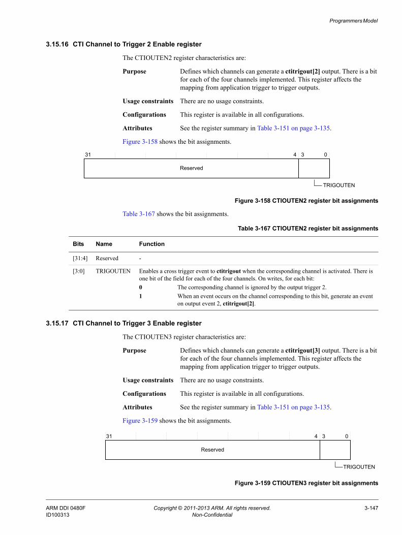
Programmers Model
3.15.16 CTI Channel to Trigger 2 Enable register
The CTIOUTEN2 register characteristics are:
Purpose Defines which channels can generate a ctitrigout[2] output. There is a bit for each of the four channels implemented. This register affects the mapping from application trigger to trigger outputs.
Usage constraints There are no usage constraints.
Configurations This register is available in all configurations.
Attributes See the register summary in Table 3-151 on page 3-135.
Figure 3-158 shows the bit assignments.
Figure 3-158 CTIOUTEN2 register bit assignments
Table 3-167 shows the bit assignments.
3.15.17 CTI Channel to Trigger 3 Enable register
The CTIOUTEN3 register characteristics are:
Purpose Defines which channels can generate a ctitrigout[3] output. There is a bit for each of the four channels implemented. This register affects the mapping from application trigger to trigger outputs.
Usage constraints There are no usage constraints.
Configurations This register is available in all configurations.
Attributes See the register summary in Table 3-151 on page 3-135.
Figure 3-159 shows the bit assignments.
Figure 3-159 CTIOUTEN3 register bit assignments
31 4 3 0
TRIGOUTEN
Reserved
Table 3-167 CTIOUTEN2 register bit assignments
Bits Name Function
[31:4] Reserved -
[3:0] TRIGOUTEN Enables a cross trigger event to ctitrigout when the corresponding channel is activated. There is one bit of the field for each of the four channels. On writes, for each bit:0 The corresponding channel is ignored by the output trigger 2.1 When an event occurs on the channel corresponding to this bit, generate an event
on output event 2, ctitrigout[2].
31 4 3 0
TRIGOUTEN
Reserved
ARM DDI 0480F Copyright © 2011-2013 ARM. All rights reserved. 3-147ID100313 Non-Confidential
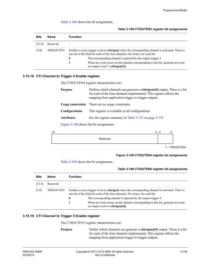
Programmers Model
Table 3-168 shows the bit assignments.
3.15.18 CTI Channel to Trigger 4 Enable register
The CTIOUTEN4 register characteristics are:
Purpose Defines which channels can generate a ctitrigout[4] output. There is a bit for each of the four channels implemented. This register affects the mapping from application trigger to trigger outputs.
Usage constraints There are no usage constraints.
Configurations This register is available in all configurations.
Attributes See the register summary in Table 3-151 on page 3-135.
Figure 3-160 shows the bit assignments.
Figure 3-160 CTIOUTEN4 register bit assignments
Table 3-169 shows the bit assignments.
3.15.19 CTI Channel to Trigger 5 Enable register
The CTIOUTEN5 register characteristics are:
Purpose Define which channels can generate a ctitrigout[5] output. There is a bit for each of the four channels implemented. This register affects the mapping from application trigger to trigger outputs.
Table 3-168 CTIOUTEN3 register bit assignments
Bits Name Function
[31:4] Reserved -
[3:0] TRIGOUTEN Enables a cross trigger event to ctitrigout when the corresponding channel is activated. There is one bit of the field for each of the four channels. On writes, for each bit: 0 The corresponding channel is ignored by the output trigger 3.1 When an event occurs on the channel corresponding to this bit, generate an event
on output event 3, ctitrigout[3].
31 4 3 0
TRIGOUTEN
Reserved
Table 3-169 CTIOUTEN4 register bit assignments
Bits Name Function
[31:4] Reserved -
[3:0] TRIGOUTEN Enables a cross trigger event to ctitrigout when the corresponding channel is activated. There is one bit of the field for each of the four channels. On writes, for each bit: 0 The corresponding channel is ignored by the output trigger 4.1 When an event occurs on the channel corresponding to this bit, generate an event
on output event 4, ctitrigout[4].
ARM DDI 0480F Copyright © 2011-2013 ARM. All rights reserved. 3-148ID100313 Non-Confidential

Programmers Model
Usage constraints There are no usage constraints.
Configurations This register is available in all configurations.
Attributes See the register summary in Table 3-151 on page 3-135.
Figure 3-161 shows the bit assignments.
Figure 3-161 CTIOUTEN5 register bit assignments
Table 3-170 shows the bit assignments.
3.15.20 CTI Channel to Trigger 6 Enable register
The CTIOUTEN6 register characteristics are:
Purpose Defines which channels can generate a ctitrigout[6] output. There is a bit for each of the four channels implemented. This register affects the mapping from application trigger to trigger outputs.
Usage constraints There are no usage constraints.
Configurations This register is available in all configurations.
Attributes See the register summary in Table 3-151 on page 3-135.
Figure 3-162 shows the bit assignments.
Figure 3-162 CTIOUTEN6 register bit assignments
31 4 3 0
TRIGOUTEN
Reserved
Table 3-170 CTIOUTEN5 register bit assignments
Bits Name Function
[31:4] Reserved -
[3:0] TRIGOUTEN Enables a cross trigger event to ctitrigout when the corresponding channel is activated. There is one bit of the field for each of the four channels. On writes, for each bit: 0 The corresponding channel is ignored by the output trigger 5.1 When an event occurs on the channel corresponding to this bit, generate an event
on output event 5, ctitrigout[5].
31 4 3 0
TRIGOUTEN
Reserved
ARM DDI 0480F Copyright © 2011-2013 ARM. All rights reserved. 3-149ID100313 Non-Confidential

Programmers Model
Table 3-171 shows the bit assignments.
3.15.21 CTI Channel to Trigger 7 Enable register
The CTIOUTEN7 register characteristics are:
Purpose Defines which channels can generate a ctitrigout[7] output. There is a bit for each of the four channels implemented. This register affects the mapping from application trigger to trigger outputs.
Usage constraints There are no usage constraints.
Configurations This register is available in all configurations.
Attributes See the register summary in Table 3-151 on page 3-135.
Figure 3-163 shows the bit assignments.
Figure 3-163 CTIOUTEN7 register bit assignments
Table 3-172 shows the bit assignments.
3.15.22 CTI Trigger In Status register
The CTITRIGINSTATUS register characteristics are:
Purpose Provides the status of the ctitrigin inputs.
Usage constraints There are no usage constraints.
Table 3-171 CTIOUTEN6 register bit assignments
Bits Name Function
[31:4] Reserved -
[3:0] TRIGOUTEN Enables a cross trigger event to ctitrigout when the corresponding channel is activated. There is one bit of the field for each of the four channels. On writes, for each bit: 0 The corresponding channel is ignored by the output trigger 6.1 When an event occurs on the channel corresponding to this bit, generate an event
on output event 6, ctitrigout[6].
31 4 3 0
TRIGOUTEN
Reserved
Table 3-172 CTIOUTEN7 register bit assignments
Bits Name Function
[31:4] Reserved -
[3:0] TRIGOUTEN Enables a cross trigger event to ctitrigout when the corresponding channel is activated. There is one bit of the field for each of the four channels. On writes, for each bit: 0 The corresponding channel is ignored by the output trigger 7.1 When an event occurs on the channel corresponding to this bit, generate an event
on output event 7, ctitrigout[7].
ARM DDI 0480F Copyright © 2011-2013 ARM. All rights reserved. 3-150ID100313 Non-Confidential

Programmers Model
Configurations This register is available in all configurations.
Attributes See the register summary in Table 3-151 on page 3-135.
Figure 3-164 shows the bit assignments.
Figure 3-164 CTITRIGINSTATUS register bit assignments
Table 3-173 shows the bit assignments.
3.15.23 CTI Trigger Out Status register
The CTITRIGOUTSTATUS register characteristics are:
Purpose Provides the status of the ctitrigout outputs.
Usage constraints There are no usage constraints.
Configurations This register is available in all configurations.
Attributes See the register summary in Table 3-151 on page 3-135.
Figure 3-165 shows the bit assignments.
Figure 3-165 CTITRIGOUTSTATUS register bit assignments
Table 3-174 shows the bit assignments.
31 0
Reserved
78
TRIGINSTATUS
Table 3-173 CTITRIGINSTATUS register bit assignments
Bits Name Function
[31:8] Reserved -
[7:0] TRIGINSTATUS Shows the status of the ctitrigin inputs. There is one bit of the field for each trigger input.1 ctitrigin is active.0 ctitrigin is inactive.Because the register provides a view of the raw ctitrigin inputs, the reset value is UNKNOWN.
31 0
Reserved
78
TRIGOUTSTATUS
Table 3-174 CTITRIGOUTSTATUS register bit assignments
Bits Name Function
[31:8] Reserved -
[7:0] TRIGOUTSTATUS Shows the status of the ctitrigout outputs. There is one bit of the field for each trigger output.1 ctitrigout is active.0 ctitrigout is inactive.
ARM DDI 0480F Copyright © 2011-2013 ARM. All rights reserved. 3-151ID100313 Non-Confidential
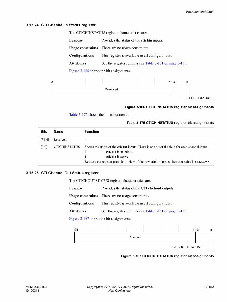
Programmers Model
3.15.24 CTI Channel In Status register
The CTICHINSTATUS register characteristics are:
Purpose Provides the status of the ctichin inputs.
Usage constraints There are no usage constraints.
Configurations This register is available in all configurations.
Attributes See the register summary in Table 3-151 on page 3-135.
Figure 3-166 shows the bit assignments.
Figure 3-166 CTICHINSTATUS register bit assignments
Table 3-175 shows the bit assignments.
3.15.25 CTI Channel Out Status register
The CTICHOUTSTATUS register characteristics are:
Purpose Provides the status of the CTI ctichout outputs.
Usage constraints There are no usage constraints.
Configurations This register is available in all configurations.
Attributes See the register summary in Table 3-151 on page 3-135.
Figure 3-167 shows the bit assignments.
Figure 3-167 CTICHOUTSTATUS register bit assignments
31 0
Reserved
CTICHINSTATUS
4 3
Table 3-175 CTICHINSTATUS register bit assignments
Bits Name Function
[31:4] Reserved -
[3:0] CTICHINSTATUS Shows the status of the ctichin inputs. There is one bit of the field for each channel input.0 ctichin is inactive.1 ctichin is active.Because the register provides a view of the raw ctichin inputs, the reset value is UNKNOWN.
31 0
Reserved
CTICHOUTSTATUS
4 3
ARM DDI 0480F Copyright © 2011-2013 ARM. All rights reserved. 3-152ID100313 Non-Confidential

Programmers Model
Table 3-176 shows the bit assignments.
3.15.26 Enable CTI Channel Gate register
The CTIGATE register characteristics are:
Purpose Prevents the channels from propagating through the CTM to other CTIs. This enables local cross-triggering, for example for causing an interrupt when the ETM trigger occurs. It can be used effectively with CTIAPPSET, CTIAPPCLEAR, and CTIAPPPULSE for asserting trigger outputs by asserting channels, without affecting the rest of the system. On reset, this register is 0xF, and channel propagation is enabled.
Usage constraints There are no usage constraints.
Configurations This register is available in all configurations.
Attributes See the register summary in Table 3-151 on page 3-135.
Figure 3-168 shows the bit assignments.
Figure 3-168 CTIGATE register bit assignments
Table 3-177 shows the bit assignments.
Table 3-176 CTICHOUTSTATUS register bit assignments
Bits Name Function
[31:4] Reserved -
[3:0] CTICHOUTSTATUS Shows the status of the ctichout outputs. There is one bit of the field for each channel output.0 ctichout is inactive.1 ctichout is active.
31 4 3 2 1 0
CTIGATEEN2CTIGATEEN1CTIGATEEN0
CTIGATEEN3
Reserved
Table 3-177 CTIGATE register bit assignments
Bits Name Function
[31:4] Reserved -
[3] CTIGATEEN3 Enable ctichout3. Set to 0 to disable channel propagation.
[2] CTIGATEEN2 Enable ctichout2. Set to 0 to disable channel propagation.
[1] CTIGATEEN1 Enable ctichout1. Set to 0 to disable channel propagation.
[0] CTIGATEEN0 Enable ctichout0. Set to 0 to disable channel propagation.
ARM DDI 0480F Copyright © 2011-2013 ARM. All rights reserved. 3-153ID100313 Non-Confidential

Programmers Model
3.15.27 External Multiplexer Control register
The ASICCTL register characteristics are:
Purpose IMPLEMENTATION DEFINED ASIC control. The value written to the register is output on asicctl[7:0].
Usage constraints There are no usage constraints.
Configurations This register is available in all configurations.
Attributes See the register summary in Table 3-151 on page 3-135.
Figure 3-169 shows the bit assignments.
Figure 3-169 ASICCTL register bit assignments
Table 3-178 shows the bit assignments.
3.15.28 Integration Test Channel Input Acknowledge register
The ITCHINACK register characteristics are:
Purpose Sets the value of the ctchinack outputs.
Usage constraints There are no usage constraints.
Configurations This register is available in all configurations.
Attributes See the register summary in Table 3-151 on page 3-135.
Figure 3-170 shows the bit assignments.
Figure 3-170 ITCHINACK register bit assignments
ASICCTL
31 8 7 0
Reserved
Table 3-178 ASICCTL register bit assignments
Bits Name Function
[31:8] Reserved -
[7:0] ASICCTL When external multiplexing is implemented for trigger signals, then the number of multiplexed signals on each trigger must be shown in the Device ID Register. This is done using a Verilog define EXTMUXNUM.
31 4 3 0
Reserved
CTCHINACK
ARM DDI 0480F Copyright © 2011-2013 ARM. All rights reserved. 3-154ID100313 Non-Confidential

Programmers Model
Table 3-179 shows the bit assignments.
3.15.29 Integration Test Trigger Input Acknowledge register
The ITTRIGINACK register characteristics are:
Purpose Sets the value of the cttriginack outputs.
Usage constraints There are no usage constraints.
Configurations This register is available in all configurations.
Attributes See the register summary in Table 3-151 on page 3-135.
Figure 3-171 shows the bit assignments.
Figure 3-171 ITTRIGINACK register bit assignments
Table 3-180 shows the bit assignments.
3.15.30 Integration Test Channel Output register
The ITCHOUT register characteristics are:
Purpose Sets the value of the ctchout outputs.
Usage constraints There are no usage constraints.
Configurations This register is available in all configurations.
Attributes See the register summary in Table 3-151 on page 3-135.
Figure 3-172 shows the bit assignments.
Figure 3-172 ITCHOUT register bit assignments
Table 3-179 ITCHINACK register bit assignments
Bits Name Function
[31:4] Reserved -
[3:0] CTCHINACK Sets the value of the ctchinack outputs.
CTTRIGINACK
31 8 7 0
Reserved
Table 3-180 ITTRIGINACK register bit assignments
Bits Name Function
[31:8] Reserved -
[7:0] CTTRIGINACK Sets the value of the cttriginack outputs.
CTCHOUT
31 4 3 0
Reserved
ARM DDI 0480F Copyright © 2011-2013 ARM. All rights reserved. 3-155ID100313 Non-Confidential

Programmers Model
Table 3-181 shows the bit assignments.
3.15.31 Integration Test Trigger Output register
The ITTRIGOUT register characteristics are:
Purpose Sets the value of the cttrigout outputs.
Usage constraints There are no usage constraints.
Configurations This register is available in all configurations.
Attributes See the register summary in Table 3-151 on page 3-135.
Figure 3-173 shows the bit assignments.
Figure 3-173 ITTRIGOUT register bit assignments
Table 3-182 shows the bit assignments.
3.15.32 Integration Test Channel Output Acknowledge register
The ITCHOUTACK register characteristics are:
Purpose Reads the values of the ctchoutack inputs.
Usage constraints There are no usage constraints.
Configurations This register is available in all configurations.
Attributes See the register summary in Table 3-151 on page 3-135.
Figure 3-174 on page 3-157 shows the bit assignments.
Table 3-181 ITCHOUT register bit assignments
Bits Name Function
[31:4] Reserved -
[3:0] CTCHOUT Sets the value of the ctchout outputs.
CTTRIGOUT
31 8 7 0
Reserved
Table 3-182 ITTRIGOUT register bit assignments
Bits Name Function
[31:8] Reserved -
[7:0] CTTRIGOUT Sets the value of the cttrigout outputs.
ARM DDI 0480F Copyright © 2011-2013 ARM. All rights reserved. 3-156ID100313 Non-Confidential

Programmers Model
Figure 3-174 ITCHOUTACK register bit assignments
Table 3-183 shows the bit assignments.
3.15.33 Integration Test Trigger Output Acknowledge register
The ITTRIGOUTACK register characteristics are:
Purpose Reads the values of the cttrigoutack inputs.
Usage constraints There are no usage constraints.
Configurations This register is available in all configurations.
Attributes See the register summary in Table 3-151 on page 3-135.
Figure 3-175 shows the bit assignments.
Figure 3-175 ITTRIGOUTACK register bit assignments
Table 3-184 shows the bit assignments.
3.15.34 Integration Test Channel Input register
The ITCHIN register characteristics are:
Purpose Reads the values of the ctchin inputs.
Usage constraints There are no usage constraints.
Configurations This register is available in all configurations.
Attributes See the register summary in Table 3-151 on page 3-135.
31 4 3 0
Reserved
CTCHOUTACK
Table 3-183 ITCHOUTACK register bit assignments
Bits Name Function
[31:4] Reserved -
[3:0] CTCHOUTACK Reads the values of the ctchoutack inputs.
CTTRIGOUTACK
31 8 7 0
Reserved
Table 3-184 ITTRIGOUTACK register bit assignments
Bits Name Function
[31:8] Reserved -
[7:0] CTTRIGOUTACK Reads the value of the cttrigoutack inputs.
ARM DDI 0480F Copyright © 2011-2013 ARM. All rights reserved. 3-157ID100313 Non-Confidential

Programmers Model
Figure 3-176 shows the bit assignments.
Figure 3-176 ITCHIN register bit assignments
Table 3-185 shows the bit assignments.
3.15.35 Integration Test Trigger Input register
The ITTRIGIN register characteristics are:
Purpose Reads the values of the cttrigin inputs.
Usage constraints There are no usage constraints.
Configurations This register is available in all configurations.
Attributes See the register summary in Table 3-151 on page 3-135.
Figure 3-177 shows the bit assignments.
Figure 3-177 ITTRIGIN register bit assignments
Table 3-186 shows the bit assignments.
3.15.36 Integration Mode Control register
The ITCTRL register characteristics are:
Purpose This register enables topology detection.See the ARM® CoreSight™ Architecture Specification. This register enables the component to switch from a functional mode, the default behavior, to integration mode where the inputs and outputs of the component can be directly controlled for the purposes of integration testing and topology detection.
CTCHIN
31 4 3 0
Reserved
Table 3-185 ITCHIN register bit assignments
Bits Name Function
[31:4] Reserved -
[3:0] CTCHIN Reads the value of the ctchin inputs.
CTTRIGIN
31 8 7 0
Reserved
Table 3-186 ITTRIGIN register bit assignments
Bits Name Function
[31:8] Reserved -
[7:0] CTTRIGIN Reads the values of the cttrigin inputs.
ARM DDI 0480F Copyright © 2011-2013 ARM. All rights reserved. 3-158ID100313 Non-Confidential

Programmers Model
Note When a device is in integration mode, the intended functionality might not
be available.
After performing integration or topology detection, you must reset the system to ensure correct behavior of CoreSight SoC-400 and other connected system components that the integration or topology detection can affect.
Usage constraints There are no usage constraints.
Configurations This register is available in all configurations.
Attributes See the register summary in Table 3-151 on page 3-135.
Figure 3-178 shows the bit assignments.
Figure 3-178 ITCTRL register bit assignments
Table 3-187 shows the bit assignments.
3.15.37 Claim Tag Set register
The CLAIMSET register characteristics are:
Purpose Software can use the claim tag to coordinate application and debugger access to trace unit functionality. The claim tags have no effect on the operation of the component. The CLAIMSET register sets bits in the claim tag, and determines the number of claim bits implemented.
Usage constraints There are no usage constraints.
Configurations This register is available in all configurations.
Attributes See the register summary in Table 3-151 on page 3-135.
Figure 3-179 on page 3-160 shows the bit assignments.
31 1 0
Reserved
IME
Table 3-187 ITCTRL register bit assignments
Bits Name Function
[31:1] Reserved -
[0] IME Integration Mode Enable. 0 Disable integration mode.1 Enable integration mode.
ARM DDI 0480F Copyright © 2011-2013 ARM. All rights reserved. 3-159ID100313 Non-Confidential

Programmers Model
Figure 3-179 CLAIMSET register bit assignments
Table 3-188 shows the bit assignments.
3.15.38 Claim Tag Clear register
The CLAIMCLR register characteristics are:
Purpose Software can use the claim tag to coordinate application and debugger access to trace unit functionality. The claim tags have no effect on the operation of the component. The CLAIMCLR register sets the bits in the claim tag to 0 and determines the current value of the claim tag.
Usage constraints There are no usage constraints.
Configurations This register is available in all configurations.
Attributes See the register summary in Table 3-151 on page 3-135.
Figure 3-180 shows the bit assignments.
Figure 3-180 CLAIMCLR register bit assignments
Table 3-189 shows the bit assignments.
Reserved
31 4 3 0
SET
Table 3-188 CLAIMSET register bit assignments
Bits Name Function
[31:4] Reserved -
[3:0] SET On reads, for each bit: 1 Claim tag bit is implementedOn writes, for each bit:0 Has no effect.1 Sets the relevant bit of the claim tag.
Reserved
31 4 3 0
CLR
Table 3-189 CLAIMCLR register bit assignments
Bits Name Function
[31:4] Reserved -
[3:0] CLR On reads, for each bit: 0 Claim tag bit is not set.1 Claim tag bit is set.On writes, for each bit: 0 Has no effect.1 Clears the relevant bit of the claim tag.
ARM DDI 0480F Copyright © 2011-2013 ARM. All rights reserved. 3-160ID100313 Non-Confidential

Programmers Model
3.15.39 Lock Access Register
The LAR characteristics are:
Purpose Controls write access from self-hosted, on-chip accesses. The LAR does not affect the accesses that use the external debugger interface.
Usage constraints There are no usage constraints.
Configurations This register is available in all configurations.
Attributes See the register summary in Table 3-151 on page 3-135.
Figure 3-181 shows the bit assignments.
Figure 3-181 LAR bit assignments
Table 3-190 shows the bit assignments.
3.15.40 Lock Status Register
The LSR characteristics are:
Purpose Indicates the status of the lock control mechanism. This lock prevents accidental writes. When locked, write accesses are denied for all registers except for the LAR. The lock registers do not affect accesses from the external debug interface. This register reads as 0 when accessed from the external debug interface.
Usage constraints There are no usage constraints.
Configurations This register is available in all configurations.
Attributes See the register summary in Table 3-151 on page 3-135.
Figure 3-182 shows the bit assignments.
Figure 3-182 LSR bit assignments
31 0
KEY
Table 3-190 LAR bit assignments
Bits Name Function
[31:0] KEY Software lock key value. 0xC5ACCE55 Clear the software lock.All other write values set the software lock.
Reserved
31 03 12
SLISLKnTT
ARM DDI 0480F Copyright © 2011-2013 ARM. All rights reserved. 3-161ID100313 Non-Confidential
Programmers Model
Table 3-191 shows the bit assignments.
3.15.41 Authentication Status register
The AUTHSTATUS register characteristics are:
Purpose Reports the required security level and present status.
Usage constraints There are no usage constraints.
Configurations This register is available in all configurations.
Attributes See the register summary in Table 3-151 on page 3-135.
Figure 3-183 shows the bit assignments.
Figure 3-183 AUTHSTATUS register bit assignments
Table 3-192 shows the bit assignments.
Table 3-191 LSR bit assignments
Bits Name Function
[31:3] Reserved -
[2] nTT Register size indicator. Always 0. Indicates that the LAR is implemented as 32-bit.
[1] SLK Software Lock Status. Returns the present lock status of the device, from the current interface.0 Indicates that write operations are permitted from this interface.1 Indicates that write operations are not permitted from this interface. Read
operations are permitted.
[0] SLI Software Lock Implemented. Indicates that a lock control mechanism is present from this interface.0 Indicates that a lock control mechanism is not present from this interface. Write
operations to the LAR are ignored.1 Indicates that a lock control mechanism is present from this interface.
31 8 7 6 5 4 3 2 0
Reserved
NSIDNSNIDSIDSNID
1
Table 3-192 AUTHSTATUS register bit assignments
Bits Name Function
[31:8] Reserved -
[7:6] SNID Always 0b00. The security level for secure non-invasive debug is not implemented or is controlled elsewhere.
ARM DDI 0480F Copyright © 2011-2013 ARM. All rights reserved. 3-162ID100313 Non-Confidential

Programmers Model
3.15.42 Device Configuration register
The DEVID register characteristics are:
Purpose Indicates the capabilities of the component.
Usage constraints There are no usage constraints.
Configurations This register is available in all configurations.
Attributes See the register summary in Table 3-151 on page 3-135.
Figure 3-184 shows the bit assignments.
Figure 3-184 DEVID register bit assignments
Table 3-193 shows the bit assignments.
3.15.43 Device Type Identifier register
The DEVTYPE register characteristics are:
Purpose Provides a debugger with information about the component when the Part Number field is not recognized. The debugger can then report this information.
[5:4] SID Always 0b00 Secure invasive debug is not implemented or is controlled elsewhere.
[3:2] NSNID Indicates the security level for non-secure non-invasive debug:0b10 Disabled.0b11 Enabled.
[1:0] NSID Indicates the security level for non-secure invasive debug:0b10 Disabled.0b11 Enabled.
Table 3-192 AUTHSTATUS register bit assignments (continued)
Bits Name Function
31 20 19 16 15 8 7 5 4 0
NUMTRIG
Reserved
EXTMUXNUMNUMCHReserved
Table 3-193 DEVID register bit assignments
Bits Name Function
[31:20] Reserved -
[19:16] NUMCH Number of ECT channels available.
[15:8] NUMTRIG Number of ECT triggers available.
[7:5] Reserved -
[4:0] EXTMUXNUM Indicates the number of multiplexers available on Trigger Inputs and Trigger Outputs that are using asicctl. The default value of 0b00000 indicates that no multiplexing is present.This value of this bit depends on the Verilog define EXTMUXNUM that you must change accordingly.
ARM DDI 0480F Copyright © 2011-2013 ARM. All rights reserved. 3-163ID100313 Non-Confidential

Programmers Model
Usage constraints There are no usage constraints.
Configurations This register is available in all configurations.
Attributes See the register summary in Table 3-151 on page 3-135.
Figure 3-185 shows the bit assignments.
Figure 3-185 DEVTYPE register bit assignments
Table 3-194 shows the bit assignments.
3.15.44 Peripheral ID4 Register
The PIDR4 characteristics are:
Purpose Part of the set of peripheral identification registers. Contains part of the designer identity and the memory size.
Usage constraints There are no usage constraints.
Configurations This register is available in all configurations.
Attributes See the register summary in Table 3-151 on page 3-135.
Figure 3-186 shows the bit assignments.
Figure 3-186 PIDR4 bit assignments
31 0
Reserved
7
SUB
8 4
MAJOR
3
Table 3-194 DEVTYPE register bit assignments
Bits Name Function
[31:8] Reserved -
[7:4] SUB Sub-classification of the type of the debug component as specified in the ARM® CoreSight™ Architecture Specification within the major classification as specified in the MAJOR field.0b0001 Indicates that this component is a cross-triggering component.
[3:0] MAJOR Major classification of the type of the debug component as specified in the ARM® CoreSight™ Architecture Specification for this debug and trace component.0b0100 Indicates that this component allows a debugger to control other components in a
CoreSight SoC-400 system.
31 0
Reserved
7
SIZE
8 4
DES_2
3
ARM DDI 0480F Copyright © 2011-2013 ARM. All rights reserved. 3-164ID100313 Non-Confidential

Programmers Model
Table 3-195 shows the bit assignments.
3.15.45 Peripheral ID0 Register
The PIDR0 characteristics are:
Purpose Part of the set of peripheral identification registers. Contains part of the designer-specific part number.
Usage constraints There are no usage constraints.
Configurations This register is available in all configurations.
Attributes See the register summary in Table 3-151 on page 3-135.
Figure 3-187 shows the bit assignments.
Figure 3-187 PIDR0 bit assignments
Table 3-196 shows the bit assignments.
3.15.46 Peripheral ID1 Register
The PIDR1 characteristics are:
Purpose Part of the set of peripheral identification registers. Contains part of the designer-specific part number and part of the designer identity.
Usage constraints There are no usage constraints.
Configurations This register is available in all configurations.
Attributes See the register summary in Table 3-151 on page 3-135.
Table 3-195 PIDR4 bit assignments
Bits Name Function
[31:8] Reserved -
[7:4] SIZE Always 0b0000. Indicates that the device only occupies 4KB of memory.
[3:0] DES_2 Together, PIDR1.DES_0, PIDR2.DES_1, and PIDR4.DES_2 identify the designer of the component.0b0100 JEDEC continuation code.
31 0
Reserved
78
PART_0
Table 3-196 PIDR0 bit assignments
Bits Name Function
[31:8] Reserved -
[7:0] PART_0 Bits[7:0] of the 12-bit part number of the component. The designer of the component assigns this part number.0x06 Indicates bits[7:0] of the part number of the component.
ARM DDI 0480F Copyright © 2011-2013 ARM. All rights reserved. 3-165ID100313 Non-Confidential

Programmers Model
Figure 3-188 shows the bit assignments.
Figure 3-188 PIDR1 bit assignments
Table 3-197 shows the bit assignments.
3.15.47 Peripheral ID2 Register
The PIDR2 characteristics are:
Purpose Part of the set of peripheral identification registers. Contains part of the designer identity and the product revision.
Usage constraints There are no usage constraints.
Configurations This register is available in all configurations.
Attributes See the register summary in Table 3-151 on page 3-135.
Figure 3-189 shows the bit assignments.
Figure 3-189 PIDR2 bit assignments
Table 3-198 shows the bit assignments.
31 0
Reserved
78
PART_1
4 3
DES_0
Table 3-197 PIDR1 bit assignments
Bits Name Function
[31:8] Reserved -
[7:4] DES_0 Together, PIDR1.DES_0, PIDR2.DES_1, and PIDR4.DES_2 identify the designer of the component.0b1011 ARM. Bits[3:0] of the JEDEC JEP106 Identity Code.
[3:0] PART_1 Bits[11:8] of the 12-bit part number of the component. The designer of the component assigns this part number.0b1001 Indicates bits[11:8] of the part number of the component.
31 0
Reserved
7
REVISION
8 4
DES_1
3 2
JEDEC
Table 3-198 PIDR2 bit assignments
Bits Name Function
[31:8] Reserved -
ARM DDI 0480F Copyright © 2011-2013 ARM. All rights reserved. 3-166ID100313 Non-Confidential

Programmers Model
3.15.48 Peripheral ID3 Register
The PIDR3 characteristics are:
Purpose Part of the set of peripheral identification registers. Contains the REVAND and CMOD fields.
Usage constraints There are no usage constraints.
Configurations This register is available in all configurations.
Attributes See the register summary in Table 3-151 on page 3-135.
Figure 3-190 shows the bit assignments.
Figure 3-190 PIDR3 bit assignments
Table 3-199 shows the bit assignments.
3.15.49 Component ID0 Register
The CIDR0 characteristics are:
Purpose A component identification register that indicates the presence of identification registers.
Usage constraints There are no usage constraints.
[7:4] REVISION 0b0100 This device is at r0p5.
[3] JEDEC Always 1. Indicates that the JEDEC-assigned designer ID is used.
[2:0] DES_1 Together, PIDR1.DES_0, PIDR2.DES_1, and PIDR4.DES_2 identify the designer of the component.0b011 ARM. Bits[6:4] of the JEDEC JEP106 Identity Code.
Table 3-198 PIDR2 bit assignments (continued)
Bits Name Function
31 0
Reserved
7
REVAND
8 4
CMOD
3
Table 3-199 PIDR3 bit assignments
Bits Name Function
[31:8] Reserved -
[7:4] REVAND Indicates minor errata fixes specific to the revision of the component being used, for example metal fixes after implementation. In most cases, this field is 0b0000. ARM recommends that the component designers ensure that a metal fix can change this field if required, for example, by driving it from registers that reset to 0b0000.0b0000 Indicates that there are no errata fixes to this component.
[3:0] CMOD Customer Modified. Indicates whether the customer has modified the behavior of the component. In most cases, this field is 0b0000. Customers change this value when they make authorized modifications to this component.0b0000 Indicates that the customer has not modified this component.
ARM DDI 0480F Copyright © 2011-2013 ARM. All rights reserved. 3-167ID100313 Non-Confidential

Programmers Model
Configurations This register is available in all configurations.
Attributes See the register summary in Table 3-151 on page 3-135.
Figure 3-191 shows the bit assignments.
Figure 3-191 CIDR0 bit assignments
Table 3-200 shows the bit assignments.
3.15.50 Component ID1 Register
The CIDR1 characteristics are:
Purpose A component identification register that indicates the presence of identification registers. This register also indicates the component class.
Usage constraints There are no usage constraints.
Configurations This register is available in all configurations.
Attributes See the register summary in Table 3-151 on page 3-135.
Figure 3-192 shows the bit assignments.
Figure 3-192 CIDR1 bit assignments
Table 3-201 shows the bit assignments.
PRMBL_0
31 8 7 0
Reserved
Table 3-200 CIDR0 bit assignments
Bits Name Function
[31:8] Reserved -
[7:0] PRMBL_0 Preamble[0]. Contains bits[7:0] of the component identification code.0x0D Bits[7:0] of the identification code.
31 8 7 4 3 0
PRMBL_1CLASSReserved
Table 3-201 CIDR1 bit assignments
Bits Name Function
[31:8] Reserved -
[7:4] CLASS Class of the component, for example, whether the component is a ROM table or a generic CoreSight SoC-400 component. Contains bits[15:12] of the component identification code.0b1001 Indicates that the component is a CoreSight SoC-400 component.
[3:0] PRMBL_1 Preamble[1]. Contains bits[11:8] of the component identification code.0b0000 Bits[11:8] of the identification code.
ARM DDI 0480F Copyright © 2011-2013 ARM. All rights reserved. 3-168ID100313 Non-Confidential

Programmers Model
3.15.51 Component ID2 Register
The CIDR2 characteristics are:
Purpose A component identification register that indicates the presence of identification registers.
Usage constraints There are no usage constraints.
Configurations This register is available in all configurations.
Attributes See the register summary in Table 3-151 on page 3-135.
Figure 3-193 shows the bit assignments.
Figure 3-193 CIDR2 bit assignments
Table 3-202 shows the bit assignments.
3.15.52 Component ID3 Register
The CIDR3 characteristics are:
Purpose A component identification register that indicates the presence of identification registers.
Usage constraints There are no usage constraints.
Configurations This register is available in all configurations.
Attributes See the register summary in Table 3-151 on page 3-135.
Figure 3-194 shows the bit assignments.
Figure 3-194 CIDR3 bit assignments
PRMBL_2
31 8 7 0
Reserved
Table 3-202 CIDR2 bit assignments
Bits Name Function
[31:8] Reserved -
[7:0] PRMBL_2 Preamble[2]. Contains bits[23:16] of the component identification code.0x05 Bits[23:16] of the identification code.
31 0
Reserved
78
PRMBL_3
ARM DDI 0480F Copyright © 2011-2013 ARM. All rights reserved. 3-169ID100313 Non-Confidential

Programmers Model
Table 3-203 shows the bit assignments.
Table 3-203 CIDR3 bit assignments
Bits Name Function
[31:8] Reserved -
[7:0] PRMBL_3 Preamble[3]. Contains bits[31:24] of the component identification code.0xB1 Bits[31:24] of the identification code.
ARM DDI 0480F Copyright © 2011-2013 ARM. All rights reserved. 3-170ID100313 Non-Confidential

Programmers Model
3.16 DAP register summaryThis section shows the following DAP component register summaries:• JTAG-AP register summary.• AHB-AP register summary.• AXI-AP register summary on page 3-172.• APB-AP register summary on page 3-172.• Debug port register summary on page 3-173.
3.16.1 JTAG-AP register summary
Table 3-204 shows the JTAG-AP register summary.
3.16.2 AHB-AP register summary
Table 3-205 shows the AHB-AP register summary.
Table 3-204 JTAG-AP register summary
Offset Type Reset value Name
0x00 RW 0x00000000 JTAG-AP Control/Status Word register, CSW, 0x00 on page 3-175, CSW.
0x04 RW 0x00 JTAG-AP Port Select register, PORTSEL, 0x04 on page 3-176, PORTSEL.
0x08 RW 0x00 JTAG-AP Port Status register, PSTA, 0x08 on page 3-176, PSTA.
0x0C - - Reserved.
0x10 RW UNDEFINED JTAG-AP Byte FIFO registers, BFIFOn, 0x10-0x1C on page 3-177.
0x14 RW UNDEFINED
0x18 RW UNDEFINED
0x1C RW UNDEFINED
0x20-0xF8 - - Reserved, SBZ.
0xFC RO 0x24760010 JTAG-AP Identification Register, IDR on page 3-177, IDR. Required by all access ports.
Table 3-205 AHB-AP register summary
Offset Type Reset value Name
0x00 RW 0x40000002 AHB-AP Control/Status Word register, CSW, 0x00 on page 3-178, CSW.
0x04 RW 0x00000000 AHB-AP Transfer Address Register, TAR, 0x04 on page 3-180, TAR.
0x08 - - Reserved, SBZ.
0x0C RW - AHB-AP Data Read/Write register, DRW, 0x0C on page 3-180, DRW.
0x10 RW - AHB-AP Banked Data registers, BD0-BD03, 0x10-0x1C on page 3-181.
0x14 RW -
0x18 RW -
0x1C RW -
ARM DDI 0480F Copyright © 2011-2013 ARM. All rights reserved. 3-171ID100313 Non-Confidential

Programmers Model
3.16.3 AXI-AP register summary
Table 3-206 shows the AXI-AP register summary.
3.16.4 APB-AP register summary
Table 3-207 shows the APB-AP register summary.
0x20-0xF7 - - Reserved, SBZ.
0xF8 RO IMPLEMENTATION DEFINED AHB-AP Debug Base Address register, ROM, 0xF8 on page 3-181.
0xFC RO 0x64770001 AHB-AP Identification Register, IDR, 0xFC on page 3-181, IDR.
Table 3-205 AHB-AP register summary (continued)
Offset Type Reset value Name
Table 3-206 AXI-AP register summary
Offset Type Reset value Name
0x00 RW - AXI-AP Control/Status Word register on page 3-182, CSW.
0x04 RW - AXI-AP Transfer Address Register on page 3-184, TAR.
0x08 RW -
0x0C RW - AXI-AP Data RW register on page 3-185, DRW.
0x10 RW - AXI-AP Banked Data registers on page 3-185.
0x14 RW -
0x18 RW -
0x1C RW -
0x20 RW - AXI-AP ACE Barrier Transaction register on page 3-186.
0x24-0xEC - - Reserved, SBZ.
0xF0 RO - AXI-AP Debug Base Address register, BASE [63:32] on page 3-187.
0xF4 RO - AXI-AP Configuration register on page 3-188
0xF8 RO - AXI-AP Debug Base Address register, BASE [31:0] on page 3-187.
0xFC RO - AXI-AP Identification Register, IDR on page 3-188.
Table 3-207 APB-AP register summary
Offset Type Reset value Name
0x00 RW 0x00000002 APB-AP Control/Status Word register, CSW, 0x00 on page 3-189, CSW.
0x04 RW 0x00000000 APB-AP Transfer Address Register, TAR, 0x04 on page 3-190, TAR.
0x08 - - Reserved, SBZ.
0x0C RW - APB-AP Data Read/Write register, DRW, 0x0C on page 3-191, DRW.
ARM DDI 0480F Copyright © 2011-2013 ARM. All rights reserved. 3-172ID100313 Non-Confidential
Programmers Model
3.16.5 Debug port register summary
Table 3-208 shows the DP register summary, and summarizes which registers are implemented on a JTAG-DP and which are implemented on an SW-DP.
JTAG-DP register summary
Table 3-209 on page 3-174 shows all implemented registers accessible through the JTAG interface. All other Instruction Register (IR) instructions are implemented as BYPASS. An external TAP controller must be implemented in accordance with the ARM® Debug Interface Architecture Specification, ADIv5.0 to ADIv5.2, if more IR registers are required, for example, JTAG TAP boundary scan. See JTAP-DP register descriptions on page 3-202.
0x10 RW - APB-AP Banked Data registers, BD0-BD3, 0x10-0x1C on page 3-191.
0x14 RW -
0x18 RW -
0x1C RW -
0x20-0xF4 - - Reserved, SBZ.
0xF8 RO 0x80000003 APB-AP Debug Base Address register, BASE, 0xF8 on page 3-192, BASE.
0xFC RO 0x44770002 APB-AP Identification Register on page 3-192, IDR.
Table 3-207 APB-AP register summary (continued)
Offset Type Reset value Name
Table 3-208 Debug port register summary
Name JTAG-DP SW-DP Description
ABORT Yes Yes AP Abort Register. See AP Abort register, ABORT on page 3-192.
IDCODE Yes No ID Code Register. See Identification Code register, IDCODE on page 3-194.
DPIDR No Yes Debug Port Identification Register. See Debug Port Identification Register, DPIDR on page 3-194.
CTRL/STAT Yes Yes Control/Status Register. See Control/Status register, CTRL/STAT on page 3-195.
SELECT Yes Yes AP Select Register. See AP Select register, SELECT on page 3-197.
RDBUFF Yes Yes Read Buffer Register. See Read Buffer register, RDBUFF on page 3-198.
DLCR No Yes Data Link Control Register. See Data Link Control Register, DLCR (SW-DP only) on page 3-199.
TARGETID No Yes Target Identification Register. See Target Identification register, TARGETID (SW-DP only) on page 3-200.
DLPIDR No Yes Data Link Protocol Identification Register. See Data Link Protocol Identification Register, DLPIDR (SW-DP only) on page 3-201.
RESEND No Yes Read Resend Register. See Read Resend register, RESEND (SW-DP only) on page 3-202.
ARM DDI 0480F Copyright © 2011-2013 ARM. All rights reserved. 3-173ID100313 Non-Confidential

Programmers Model
Table 3-209 JTAG-DP register summary
IR instruction value JTAG-DP register DR scan width Description
0b1000 ABORT 35 JTAG-DP Abort Register, ABORT.
0b1010 DPACC 35 JTAG DP/AP Access Registers, DPACC/APACC.
0b1011 APACC 35
0b1110 IDCODE 32 JTAG Device ID Code Register, IDCODE.
0b1111 BYPASS 1 JTAG Bypass Register, BYPASS.
ARM DDI 0480F Copyright © 2011-2013 ARM. All rights reserved. 3-174ID100313 Non-Confidential
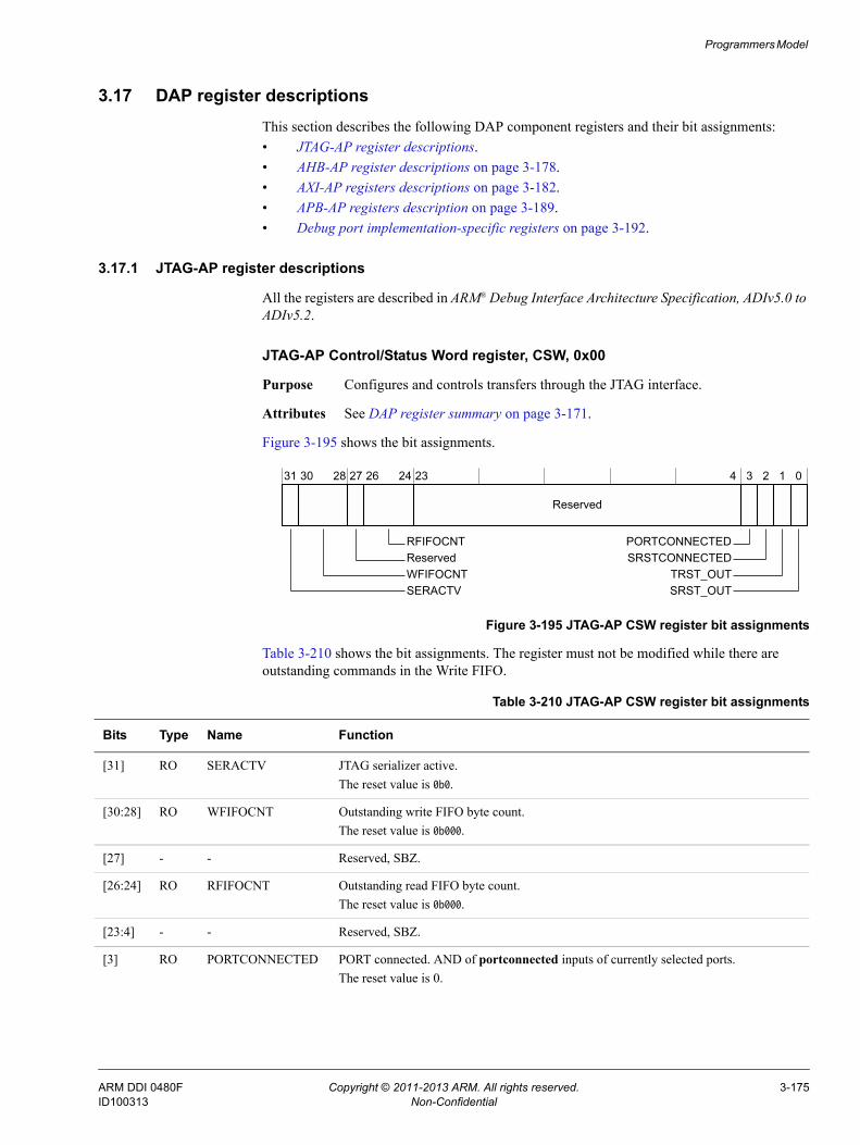
Programmers Model
3.17 DAP register descriptionsThis section describes the following DAP component registers and their bit assignments:• JTAG-AP register descriptions.• AHB-AP register descriptions on page 3-178.• AXI-AP registers descriptions on page 3-182.• APB-AP registers description on page 3-189.• Debug port implementation-specific registers on page 3-192.
3.17.1 JTAG-AP register descriptions
All the registers are described in ARM® Debug Interface Architecture Specification, ADIv5.0 to ADIv5.2.
JTAG-AP Control/Status Word register, CSW, 0x00
Purpose Configures and controls transfers through the JTAG interface.
Attributes See DAP register summary on page 3-171.
Figure 3-195 shows the bit assignments.
Figure 3-195 JTAG-AP CSW register bit assignments
Table 3-210 shows the bit assignments. The register must not be modified while there are outstanding commands in the Write FIFO.
31 30 28 27 26 24 23 4 3 2 1 0
Reserved
RFIFOCNTReservedWFIFOCNTSERACTV
PORTCONNECTEDSRSTCONNECTED
TRST_OUTSRST_OUT
Table 3-210 JTAG-AP CSW register bit assignments
Bits Type Name Function
[31] RO SERACTV JTAG serializer active.The reset value is 0b0.
[30:28] RO WFIFOCNT Outstanding write FIFO byte count.The reset value is 0b000.
[27] - - Reserved, SBZ.
[26:24] RO RFIFOCNT Outstanding read FIFO byte count.The reset value is 0b000.
[23:4] - - Reserved, SBZ.
[3] RO PORTCONNECTED PORT connected. AND of portconnected inputs of currently selected ports.The reset value is 0.
ARM DDI 0480F Copyright © 2011-2013 ARM. All rights reserved. 3-175ID100313 Non-Confidential

Programmers Model
JTAG-AP Port Select register, PORTSEL, 0x04
Purpose Enables ports if connected and the slave port is currently enabled. The Port Select register must be written when the following conditions are met:• The TCK engine is idle.• SERACTV is 0.• WFIFO and WFIFOCNT are 0, that is, they are empty.Writing at other times can generate UNPREDICTABLE results.
Attributes See DAP register summary on page 3-171.
Figure 3-196 shows the bit assignments.
Figure 3-196 JTAG-AP Port Select register bit assignments
Table 3-211 shows the bit assignments.
JTAG-AP Port Status register, PSTA, 0x08
Purpose A sticky register that captures the state of a connected and selected port on every clock cycle. If a connected and selected port is disabled or powered down, even transiently, the corresponding bit in the Port Status register is set. It remains 1 until the corresponding bit is set o 1.
Attributes See DAP register summary on page 3-171.
[2] RO SRSTCONNECTEDa SRST connected.AND of srstconnected inputs of currently selected ports. If multiple ports are selected, it is the AND of all the srstconnected inputs from the selected ports.The reset value is 0.
[1] RW TRST_OUT TRST assert, not self clearing. The JTAG TAP controller reset.The reset value is 0.
[0] RW SRST_OUT SRST assert, not self clearing. Core reset.The reset value is 0.
a. SRSTCONNECTED is a strap pin on the multiplexer inputs. It is set to 1 to indicate that the target JTAG device supports individual SRST controls.
Table 3-210 JTAG-AP CSW register bit assignments (continued)
Bits Type Name Function
0
PORTSEL
7
Reserved
31
Table 3-211 JTAG-AP Port Select register bit assignments
Bits Type Name Function
[31:8] - - Reserved SBZ.
[7:0] RW PORTSEL Port Select.The reset value is 0x00.
ARM DDI 0480F Copyright © 2011-2013 ARM. All rights reserved. 3-176ID100313 Non-Confidential

Programmers Model
Figure 3-197 shows the bit assignments.
Figure 3-197 JTAG-AP Port Status register bit assignments
Table 3-212 shows the bit assignments.
JTAG-AP Byte FIFO registers, BFIFOn, 0x10-0x1C
Purpose Word interface to one, two, three, or four parallel byte entries in the byte command FIFO, LSB first. The DAP internal bus is a 32-bit interface with no SIZE field. An address decoding designates size, because the JTAG-AP engine JTAG protocol is byte encoded. Writes to the BFIFOx that are larger than the current write FIFO depth stall on dapready in normal mode. Reads to the BFIFOx that are larger than the current read FIFO depth stall on dapready in normal mode. For reads less than the full 32 bits, the upper bits are 0. For example, for a 24-bit read, daprdata[31:24] is 0x00.
Attributes See DAP register summary on page 3-171.
JTAG-AP Identification Register, IDR
Figure 3-198 shows the bit assignments.
Figure 3-198 JTAG-AP Identification Register bit assignments
Table 3-213 shows the bit assignments.
0
PSTA
7
Reserved
31
Table 3-212 JTAG-AP Port Status register bit assignments
Bits Type Name Function
[31:8] - - Reserved, SBZ.
[7:0] RW PSTA Port Status.The reset value is 0x00.
Revision
31 28 27 24 23 17 16 15 8 7 0
JEDEC bank JEDEC code Reserved Identity value
Mem AP
Table 3-213 JTAG-AP Identification Register bit assignments
Bits Type Name Value Function
[31:28] RO Revision 0x2 r0p3
[27:24] RO JEDEC bank 0x4 Designed by ARM
[23:17] RO JEDEC code 0x3B Designed by ARM
ARM DDI 0480F Copyright © 2011-2013 ARM. All rights reserved. 3-177ID100313 Non-Confidential

Programmers Model
3.17.2 AHB-AP register descriptions
This section describes the registers used to program the AHB-AP. It contains the following registers:• AHB-AP Control/Status Word register, CSW, 0x00.• AHB-AP Transfer Address Register, TAR, 0x04 on page 3-180.• AHB-AP Data Read/Write register, DRW, 0x0C on page 3-180.• AHB-AP Banked Data registers, BD0-BD03, 0x10-0x1C on page 3-181.• AHB-AP Debug Base Address register, ROM, 0xF8 on page 3-181.• AHB-AP Identification Register, IDR, 0xFC on page 3-181.
AHB-AP Control/Status Word register, CSW, 0x00
Purpose Configures and controls transfers through the AHB interface.
Attributes See DAP register summary on page 3-171.
Figure 3-199 shows the bit assignments.
Figure 3-199 AHB-AP CSW register bit assignments
[16] RO Mem AP 0x0 Is a Mem AP
[15:8] - Reserved 0x00 -
[7:0] RO Identity value 0x10 JTAG-AP
Table 3-213 JTAG-AP Identification Register bit assignments (continued)
Bits Type Name Value Function
Size
31 30 29 28 24 23 12 11 8 7 6 5 4 3 2 0
Prot Reserved Mode
TrInProgDbgStatus
AddrIncReserved
ReservedSProt
Reserved SPIStatus
22
ARM DDI 0480F Copyright © 2011-2013 ARM. All rights reserved. 3-178ID100313 Non-Confidential

Programmers Model
Table 3-214 shows the bit assignments.
Table 3-214 AHB-AP Control/Status Word register bit assignments
Bits Type Name Function
[31] - - Reserved SBZ.
[30] RW SProt Specifies that a secure transfer is requested.SProt HIGH indicates a non-secure transfer. SProt LOW indicates a secure transfer.• If this bit is LOW, and spiden is HIGH, hprot[6] is asserted LOW on an AHB transfer. • If this bit is LOW, and spiden is LOW, hprot[6] is asserted HIGH and the AHB transfer is not
initiated. • If this bit is HIGH, the state of spiden is ignored. hprot[6] is HIGH.The reset value is 1. This field is non-secure.
[29] - - Reserved, SBZ.
[28:24] RW Prot Specifies the protection signal encoding to be output on hprot[4:0].The reset value is 0b00011.This field is non secure, non-exclusive, non cacheable, non bufferable, and privileged.
[23] RO SPIStatus Indicates the status of the spiden port. If SPIStatus is LOW, no secure AHB transfers are carried out.
[22:12] - - Reserved, SBZ.
[11:8] RW Mode Specifies the mode of operation.0b0000 Normal download or upload model.0b0001-0b1111 Reserved, SBZ.The reset value is 0b0000.
[7] RO TrInProg Transfer in progress. This field indicates whether a transfer is currently in progress on the AHB master port.
[6] RO DbgStatus Indicates the status of the dbgen port. If DbgStatus is LOW, no AHB transfers are carried out.1 AHB transfers permitted.0 AHB transfers not permitted.
ARM DDI 0480F Copyright © 2011-2013 ARM. All rights reserved. 3-179ID100313 Non-Confidential

Programmers Model
AHB-AP Transfer Address Register, TAR, 0x04
Table 3-215 shows the bit assignments.
AHB-AP Data Read/Write register, DRW, 0x0C
Table 3-216 shows the bit assignments.
[5:4] RW AddrInc Auto address increment and packing mode on RW data access. Only increments if the current transaction completes without an error response and the transaction is not aborted.Auto address incrementing and packed transfers are not performed on access to Banked Data registers, 0x10-0x1C. The status of these bits is ignored in these cases.Incrementing and wrapping is performed within a 1KB address boundary, for example, for word incrementing from 0x1400-0x17FC. If the start is at 0x14A0, then the counter increments to 0x17FC, wraps to 0x1400, then continues incrementing to 0x149C.0b00 Auto increment OFF.0b00 Increment, single.Single transfer from corresponding byte lane.0b10 Increment, packed.Word Same effect as single increment.Byte or halfword Packs four 8-bit transfers or two 16-bit transfers into a 32-bit DAP transfer.
Multiple transactions are carried out on the AHB interface.0b11 Reserved, SBZ. No transfer.Size of address increment is defined by the Size field, bits [2:0].The reset value is 0b00.
[3] RW - Reserved, SBZ.The reset value is 0.
[2:0] RW Size Size of the data access to perform.0b000 8 bits.0b001 16 bits.0b010 32 bits.0b011- 0b111 Reserved, SBZ.The reset value is 0b010.
Table 3-214 AHB-AP Control/Status Word register bit assignments (continued)
Bits Type Name Function
Table 3-215 AHB-AP Transfer Address register bit assignments
Bits Type Name Function
[31:0] RW Address Address of the current transfer.The reset value is 0x00000000.
Table 3-216 AHB-AP Data Read/Write register bit assignments
Bits Type Name Function
[31:0] RW Data Write mode Data value to write for the current transfer.Read mode Data value that is read from the current transfer.
ARM DDI 0480F Copyright © 2011-2013 ARM. All rights reserved. 3-180ID100313 Non-Confidential

Programmers Model
AHB-AP Banked Data registers, BD0-BD03, 0x10-0x1C
Purpose BD0-BD3 provide a mechanism for directly mapping through DAP accesses to AHB transfers without having to rewrite the TAR within a four-location boundary. BD0 is RW from TA. BD1 is RW from TA+4.
Attributes See DAP register summary on page 3-171.
Table 3-217 shows the bit assignments.
AHB-AP Debug Base Address register, ROM, 0xF8
Table 3-218 shows the bit assignments.
AHB-AP Identification Register, IDR, 0xFC
Figure 3-200 shows the bit assignments.
Figure 3-200 AHB-AP Identification Register bit assignments
Table 3-217 Banked Data register bit assignments
Bits Type Name Function
[31:0] RW Data If dapcaddr[7:4] = 0x0001, it is accessing AHB-AP registers in the range 0x10-0x1C, and the derived haddr[31:0] is:Write mode Data value to write for the current transfer to external address TAR[31:4] +
dapcaddr[3:2] + 0b00.Read mode Data value that is read from the current transfer from external address TAR[31:4]
+ dapcaddr[3:2] + 0b00.Auto address incrementing is not performed on DAP accesses to BD0-BD3.Banked transfers are only supported for word transfers. Non-word banked transfers are reserved and UNPREDICTABLE. Transfer size is currently ignored for banked transfers.
Table 3-218 AHB-AP Debug Base Address register bit assignments
Bits Type Name Function
[31:0] RO Debug AHB ROM Address Base address of a ROM table. Bit[1] is always 1, and the other bits are set to the tie-off value on the static input port, rombaseaddr.The ROM provides a look-up table for system components. Set bit[0] to 1 if there are debug components on this bus.
Revision
31 28 27 24 23 17 16 15 8 7 0
JEDEC bank JEDEC code Reserved Identity value
Mem AP
ARM DDI 0480F Copyright © 2011-2013 ARM. All rights reserved. 3-181ID100313 Non-Confidential

Programmers Model
Table 3-219 shows the bit assignments.
3.17.3 AXI-AP registers descriptions
This section describes the following AXI-AP registers:• AXI-AP Control/Status Word register.• AXI-AP Transfer Address Register on page 3-184.• AXI-AP Data RW register on page 3-185.• AXI-AP Banked Data registers on page 3-185.• AXI-AP ACE Barrier Transaction register on page 3-186.• AXI-AP Debug Base Address register on page 3-187.• AXI-AP Configuration register on page 3-188.• AXI-AP Identification Register, IDR on page 3-188.
AXI-AP Control/Status Word register
Purpose Configures and controls transfers through the AXI interface.
Attributes See DAP register summary on page 3-171.
Figure 3-201 shows the bit assignments.
Figure 3-201 AXI-AP CSW register bit assignments
Table 3-219 AHB-AP Identification Register bit assignments
Bits Type Name Value Function
[31:28] RO Revision 0x7 r0p8
[27:24] RO JEDEC bank 0x4 Designed by ARM
[23:17] RO JEDEC code 0x3B Designed by ARM
[16] RO Mem AP 0x1 Is a Mem AP
[15:8] - Reserved 0x00 -
[7:0] RO Identity value 0x01 AHB-AP
Size
31 30 28 24 23 12 11 8 7 6 5 4 3 2 0
Cache Reserved Mode
TrInProgDbgStatusAddrIncReservedReserved SPIStatus
22
DbgStatus
1314
Domain
15
Prot
27
ARM DDI 0480F Copyright © 2011-2013 ARM. All rights reserved. 3-182ID100313 Non-Confidential

Programmers Model
Table 3-220 shows the bit assignments.
Table 3-220 AXI-AP CSW register bit assignments
Bits Type Name Reset value Function
[31] - Reserved - -
[30:28] RW Prot 0b011 Specifies protection encoding as AMBA AXI protocol describes.
[27:24] RW Cache 0b0000 Specifies the cache encoding as AMBA AXI protocol describes.
[23] RO SPIStatus - Indicates the status of the spiden port. If SPIStatus is LOW, then no secure AXI transfers are carried out.
[22:15] - Reserved - -
[14:13] RW Domain 0b11 Shareable transaction encoding for ACE.0b00 Non shareable.0b01 Shareable, inner domain, includes additional masters.0b10 Shareable, outer domain, also includes inner or additional
masters.0b11 Shareable, system domain, all masters included.
Note In revisions of AXI-AP prior to r0p3, this field was reset to 0b00. ARM recommends that you set this field to a valid value before issuing any AXI transactions, for compatibility with revisions prior to r0p3.
[12] RW ACEEnable 0b0 Enable ACE transactions, including barriers. 0 Disable.1 Enable.
[11:8] RW Mode 0b0000 Specifies the mode of operation:0b0000 Normal download or upload.0b0001 Barrier transaction.0b0010-0b1111 Reserved, SBZ.
[7] RO TrInProg - Transfer in progress. This field indicates whether a transfer is currently in progress on the AXI master port.
[6] RO DbgStatus Indicates the status of DBGEN port. If DbgStatus is LOW, then no AXI transfers are carried out. 0 AXI transactions are stopped.1 AXI transactions are permitted.
ARM DDI 0480F Copyright © 2011-2013 ARM. All rights reserved. 3-183ID100313 Non-Confidential

Programmers Model
AXI-AP Transfer Address Register
Purpose Defines the current address of the transfer.• For a 32-bit address, this contains the entire address value.• For an LPAE, this contains only the lower 32 bits of the address.
Attributes See DAP register summary on page 3-171.
Figure 3-202 shows the bit assignments.
Figure 3-202 AXI-AP Transfer Address register bit assignments
Table 3-221 shows the bit assignments.
[5:4] RW AddrInc 0b00 Auto address increment and packing mode on RW data access. Only increments if the current transaction completes without an Error response and the transaction is not aborted.Auto address incrementing and packed data transfers are not performed on access to banked data registers 0x10-0x1C. The status of these bits is ignored in these cases.The following values represent the increments and wraps within a 1K address boundary:0b00 Auto increment OFF.0b01 Single increment. Single transfer from byte lane.0b10 Increment packed.Word Same effect as single increment.Byte or Halfword Packs of four 8-bit transfers or two 16-bit transfers into a
32-bit DAP transfer.0b11 Reserved, no transfer.The size of address increment is defined by the Size field.
[3] - Reserved -
[2:0] RW Size 0b010 Size of the data access to perform.0b000 8-bit.0b001 16-bit.0b010 32-bit.0b011 64-bit.0b100-0b111 Reserved, SBZ.
Table 3-220 AXI-AP CSW register bit assignments (continued)
Bits Type Name Reset value Function
Address
31 0
Table 3-221 AXI-AP Transfer Address register bit assignments
Bits Type Name Reset value Function
[63:32] RW Address 0x00000000 Address of the current transfer.
[31:0] RW Address 0x00000000 Address of the current transfer.
ARM DDI 0480F Copyright © 2011-2013 ARM. All rights reserved. 3-184ID100313 Non-Confidential

Programmers Model
AXI-AP Data RW register
Purpose Stores the read data to be read for a read transfer. For a write transfer, write data must be written in the register.
Attributes See DAP register summary on page 3-171.
Figure 3-203 shows the bit assignments.
Figure 3-203 AXI-AP Data RW register bit assignments
Table 3-222 shows the bit assignments.
Note For 64-bit access, multiple accesses must be initiated to DRW to make a single AXI access.
Read The first read of DRW in a sequence initiates a memory access. The first read returns the lower 32 bits of data. Subsequent read access returns the upper 32 bits of data. If a write to the CSW or TAR is initiated before the sequence completes, then the read access is terminated, and read data is no longer available.
Write The first write to DRW specifies the lower 32 bits of data to be written. Subsequent write access specifies the upper 32 bits to be written. If a write to the CSW is initiated before the sequence completes, then the write access is not initiated on the AXI interface.• Combining partial reads and writes in a sequence terminates the earlier
access. Also, the latest access is not recognized.• Any write access to the CSW register, TAR, or to any other register in the
AP during a sequence terminates the ongoing access. Also, the current access is not recognized.
• If a write sequence is terminated, then there is no write on the AXI interface.
AXI-AP Banked Data registers
Purpose BD0-3 provide a mechanism for direct mapping through DAP accesses to AXI transfers without having to rewrite the TAR within a 4-location boundary. For example, BD0 reads and writes from TAR. BD1 reads and writes from TAR+4. This is applicable for a 32-bit access.
Attributes See DAP register summary on page 3-171.
Figure 3-204 on page 3-186 shows the bit assignments.
Data
31 0
Table 3-222 AXI-AP Data RW register bit assignments
Bits Type Name Function
[31:0] RW Data For 32-bit data access on the AXI-interface, store or write the 32 bits of data into this register once.Read mode Data value read from the current transfer.Write mode Data value to write for the current transfer.
ARM DDI 0480F Copyright © 2011-2013 ARM. All rights reserved. 3-185ID100313 Non-Confidential

Programmers Model
Figure 3-204 AXI-AP Banked DATA register bit assignments
Table 3-223 shows the bit assignments.
AXI-AP ACE Barrier Transaction register
Purpose Enables or disables the ACE barrier transactions.
Attributes See DAP register summary on page 3-171.
Figure 3-205 shows the bit assignments.
Figure 3-205 ACE Barrier Transaction register bit assignments
Table 3-224 shows the bit assignments.
Data
31 0
Table 3-223 AXI-AP Banked Data registers bit assignments
Bits Type Name Function
[31:0] RW Data If dapcaddr[7:4] = 0x0001, it is accessing AXI-AP registers in the range 0x10-0x1C, and the derived ADDR[ADDR_WIDTH-1:0] in RW, 32-bit mode is as follows:• For a 32-bit address mode, the external address is TAR[31:4] + DAPADDR[3:2] + 0b00.• For the LPAE mode, the external address is TAR[63:4] + DAPADDR[3:2] + 0b00.Auto address incrementing is not performed on DAP accesses to BD0-BD3.Banked transfers are only supported for word transfers for 32-bit data. Non-word banked transfers are reserved and UNPREDICTABLE. Transfer size is ignored for banked transfers.
Reserved
31 03 12
BarTranTrgBarTran
Table 3-224 ACE Barrier Transaction register bit assignments
Bits Type Name Reset value Function
[31:3] - Reserved -
[2:1] RW BarTran 0b00 Barrier transactions.0b00 Barrier with normal access.0b01 Memory barrier.0b10 Reserved.0b11 Synchronization barrier.
[0] RW TrgBarTran 0b0 The possible values are:0 Disable barrier transaction.1 Enable barrier transaction.
ARM DDI 0480F Copyright © 2011-2013 ARM. All rights reserved. 3-186ID100313 Non-Confidential
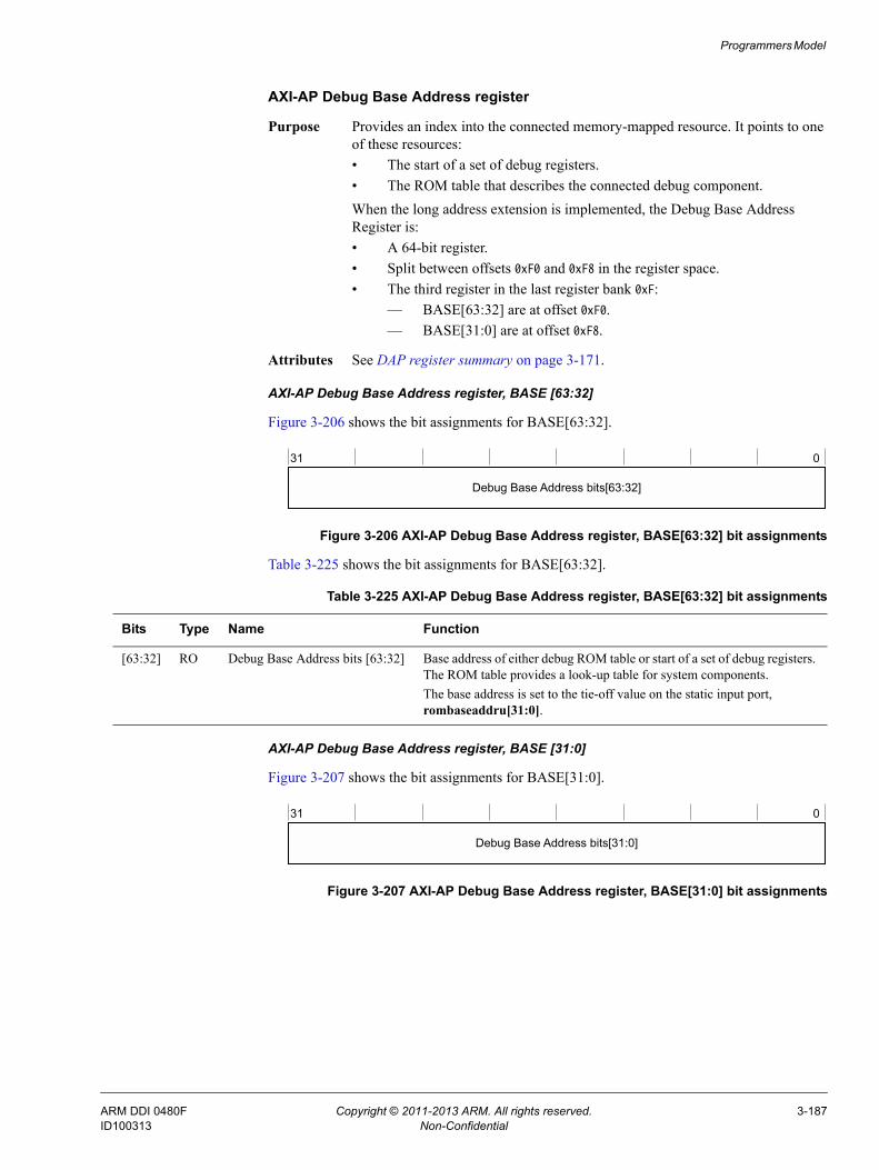
Programmers Model
AXI-AP Debug Base Address register
Purpose Provides an index into the connected memory-mapped resource. It points to one of these resources:• The start of a set of debug registers.• The ROM table that describes the connected debug component.When the long address extension is implemented, the Debug Base Address Register is:• A 64-bit register.• Split between offsets 0xF0 and 0xF8 in the register space.• The third register in the last register bank 0xF:
— BASE[63:32] are at offset 0xF0. — BASE[31:0] are at offset 0xF8.
Attributes See DAP register summary on page 3-171.
AXI-AP Debug Base Address register, BASE [63:32]
Figure 3-206 shows the bit assignments for BASE[63:32].
Figure 3-206 AXI-AP Debug Base Address register, BASE[63:32] bit assignments
Table 3-225 shows the bit assignments for BASE[63:32].
AXI-AP Debug Base Address register, BASE [31:0]
Figure 3-207 shows the bit assignments for BASE[31:0].
Figure 3-207 AXI-AP Debug Base Address register, BASE[31:0] bit assignments
Debug Base Address bits[63:32]
31 0
Table 3-225 AXI-AP Debug Base Address register, BASE[63:32] bit assignments
Bits Type Name Function
[63:32] RO Debug Base Address bits [63:32] Base address of either debug ROM table or start of a set of debug registers. The ROM table provides a look-up table for system components.The base address is set to the tie-off value on the static input port, rombaseaddru[31:0].
Debug Base Address bits[31:0]
31 0
ARM DDI 0480F Copyright © 2011-2013 ARM. All rights reserved. 3-187ID100313 Non-Confidential

Programmers Model
Table 3-226 shows the bit assignments for BASE[31:0].
AXI-AP Configuration register
Purpose Provides information about the revision.
Attributes See DAP register summary on page 3-171.
Figure 3-208 shows the bit assignments.
Figure 3-208 AXI-AP Configuration register bit assignments
Table 3-227 shows the bit assignments.
AXI-AP Identification Register, IDR
Purpose Provides information about revision.
Attributes See DAP register summary on page 3-171.
Figure 3-209 on page 3-189 shows the bit assignments.
Table 3-226 AXI-AP Debug Base Address register, BASE[31:0] bit assignments
Bits Type Name Function
[31:0] RO Debug Base Address bits [31:0] Base address of either debug ROM table or start of a set of debug registers. The ROM table provides a look-up table for system components.Bit[1] is always 1, and the other bits are set to the tie-off value on the static input port, rombaseaddrl[31:0].Set bit[0] to 1 if there are debug components on this bus.
Reserved
31 03 12
LDLABE
Table 3-227 AXI-AP Configuration register bit assignments
Bits Type Name Function
[31:3] - Reserved -
[2] RO LD Large data. Indicates support for data items larger then 32 bits.0 Only 8, 16, 32-bit data items are supported.1 Support for 64-bit data item in addition to 8, 16, 32-bit data.
[1] RO LA Long address. Indicates support for greater than 32 bits of addressing.0 32 or fewer bits of addressing. Registers 0x08 and 0xF0 are reserved.1 64 or fewer bits of addressing. TAR.l and DBAR.l occupy two locations, at 0x04
and 0x08, and at 0xF8 and 0xF0 respectively.
[0] RO BE Big-endian. Always read as 0, because AXI-AP supports little-endian.
ARM DDI 0480F Copyright © 2011-2013 ARM. All rights reserved. 3-188ID100313 Non-Confidential

Programmers Model
Figure 3-209 AXI-AP Identification Register bit assignments
Table 3-228 shows bit assignments.
3.17.4 APB-AP registers description
This section describes the following APB-AP registers:• APB-AP Control/Status Word register, CSW, 0x00.• APB-AP Transfer Address Register, TAR, 0x04 on page 3-190.• APB-AP Data Read/Write register, DRW, 0x0C on page 3-191.• APB-AP Banked Data registers, BD0-BD3, 0x10-0x1C on page 3-191.• APB-AP Debug Base Address register, BASE, 0xF8 on page 3-192.• APB-AP Identification Register on page 3-192.
APB-AP Control/Status Word register, CSW, 0x00
Purpose Configures and controls transfers through the APB interface.
Attributes See DAP register summary on page 3-171.
Figure 3-210 shows the bit assignments.
Figure 3-210 APB-AP Control/Status Word register bit assignments
Identity value
31 28 24 23 8 7 0
JEDECBank ReservedRevision
17
Code
1527
JEDECcode
16
Table 3-228 AXI-AP Identification Register bit assignments
Bits Type Name Reset value Function
[31:28] RO Revision 0x3 r1p0.
[27:24] RO JEDEC Bank 0x4 Designed by ARM.
[23:17] RO JEDEC Code 0x3B Designed by ARM.
[16] RO Mem AP 0x1 Mem AP.
[15:8] - Reserved 0x00 -
[7:0] RO Identity value 0x04 AXI-AP.
31 30 12 11 8 7 6 5 4 3 2
DbgSwEnable
Reserved Mode
0
TrInProg
DeviceEn
AddrInc
Reserved
Size
ARM DDI 0480F Copyright © 2011-2013 ARM. All rights reserved. 3-189ID100313 Non-Confidential
Programmers Model
Table 3-229 shows the bit assignments.
APB-AP Transfer Address Register, TAR, 0x04
Purpose Holds the address of the current transfer.
Attributes See DAP register summary on page 3-171.
Figure 3-211 on page 3-191 shows the bit assignments.
Table 3-229 APB Control/Status Word register bit assignments
Bits Type Name Function
[31] RW DbgSwEnable Software access enable.Drives pdbgswen to enable or disable software access to the Debug APB bus in the APB interconnect.0 Disable software access.1 Enable software access.The reset value is 0. On exit from reset, the default value is 1 to enable software access.
[30:12] - - Reserved, SBZ.
[11:8] RW Mode Specifies the mode of operation.0b0000 Normal download or upload model.0b0001-0b1111 Reserved, SBZ.The reset value is 0b0000.
[7] RO TrInProg Transfer in progress. This field indicates whether a transfer is currently in progress on the APB master port.
[6] RO DeviceEn Indicates the status of the deviceen input.• If APB-AP is connected to the Debug APB, a bus connected only to debug and trace
components, it must be permanently enabled by tying deviceen HIGH. This ensures that trace components can still be programmed when dbgen is LOW. In practice, the APB-AP is normally used in this way.
• If APB-AP is connected to a system APB dedicated to the non-secure world, deviceen must be connected to dbgen.
• If APB-AP is connected to a system APB dedicated to the secure world, deviceen must be connected to spiden.
[5:4] RW AddrInc Auto address increment and packing mode on Read or Write data access. Increment occurs in word steps. Does not increment if the transaction completes with an error response or the transaction is aborted.Auto address incrementing is not performed on accesses to banked data registers 0x10-0x1C.The status of these bits is ignored in this case.0b11 Reserved.0b10 Reserved.0b01 Increment.0b00 Auto increment OFF.The reset value is 0b00.
[3] - - Reserved, SBZ.
[2:0] RO Size Size of the access to perform. Fixed at 0b010, 32 bits.The reset value is 0b010.
ARM DDI 0480F Copyright © 2011-2013 ARM. All rights reserved. 3-190ID100313 Non-Confidential
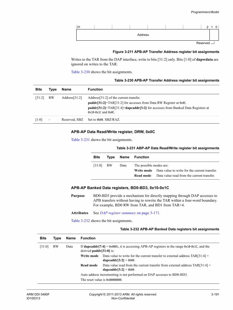
Programmers Model
Figure 3-211 APB-AP Transfer Address register bit assignments
Writes to the TAR from the DAP interface, write to bits [31:2] only. Bits [1:0] of dapwdata are ignored on writes to the TAR.
Table 3-230 shows the bit assignments.
APB-AP Data Read/Write register, DRW, 0x0C
Table 3-231 shows the bit assignments.
APB-AP Banked Data registers, BD0-BD3, 0x10-0x1C
Purpose BD0-BD3 provide a mechanism for directly mapping through DAP accesses to APB transfers without having to rewrite the TAR within a four-word boundary. For example, BD0 RW from TAR, and BD1 from TAR+4.
Attributes See DAP register summary on page 3-171.
Table 3-232 shows the bit assignments.
31 2 1 0
Reserved
Address
Table 3-230 APB-AP Transfer Address register bit assignments
Bits Type Name Function
[31:2] RW Address[31:2] Address[31:2] of the current transfer. paddr[31:2]=TAR[31:2] for accesses from Data RW Register at 0x0C.paddr[31:2]=TAR[31:4]+dapcaddr[3:2] for accesses from Banked Data Registers at 0x10-0x1C and 0x0C.
[1:0] - Reserved, SBZ Set to 0b00. SBZ/RAZ.
Table 3-231 ABP-AP Data Read/Write register bit assignments
Bits Type Name Function
[31:0] RW Data The possible modes are:Write mode Data value to write for the current transfer.Read mode Data value read from the current transfer.
Table 3-232 APB-AP Banked Data registers bit assignments
Bits Type Name Function
[31:0] RW Data If dapcaddr[7:4] = 0x0001, it is accessing APB-AP registers in the range 0x10-0x1C, and the derived paddr[31:0] is:Write mode Data value to write for the current transfer to external address TAR[31:4] +
dapcaddr[3:2] + 0b00.Read mode Data value read from the current transfer from external address TAR[31:4] +
dapcaddr[3:2] + 0b00.Auto address incrementing is not performed on DAP accesses to BD0-BD3.The reset value is 0x00000000.
ARM DDI 0480F Copyright © 2011-2013 ARM. All rights reserved. 3-191ID100313 Non-Confidential

Programmers Model
APB-AP Debug Base Address register, BASE, 0xF8
Table 3-223 on page 3-186 shows the bit assignments.
APB-AP Identification Register
Figure 3-212 shows the bit assignments.
Figure 3-212 APB-AP Identification register bit assignments
Table 3-234 shows the bit assignments.
3.17.5 Debug port implementation-specific registers
This section describes the implementation-specific registers.
AP Abort register, ABORT
Purpose Present in all debug port implementations. It forces a DAP abort on SW-DP. It also clears error and sticky flag conditions. The AP Abort is always accessible, and returns an OK response if a valid transaction is received.JTAG-DP It is at address 0x0 when the IR contains ABORT.
Table 3-233 Debug Base Address register bit assignments
Bits Type Name Function
[31:0] RO Debug APB ROM Address Base address of a ROM table. The ROM provides a look-up table for system components. Bit[1] is SBO. Set bit[0] to 1 if there are debug components on this bus. For most debug APB systems, this value is 0x80000003.
Revision
31 28 27 24 23 17 16 15 8 7 0
JEDEC bank JEDEC code Reserved Identity value
Mem AP
Table 3-234 APB-AP Identification register bit assignments
Bits Type Name
[31:28] RO Revision.0x4. This component is at r0p5.
[27:24] RO JEDEC bank. 0x4 indicates ARM.
[23:17] RO JEDEC code. 0x3B indicates ARM.
[16] RO Memory AP. 0x1 indicates a standard register map is used.
[15:8] - Reserved, SBZ.
[7:0] RO Identity value.The reset value is 0x03 for APB-AP.
ARM DDI 0480F Copyright © 2011-2013 ARM. All rights reserved. 3-192ID100313 Non-Confidential

Programmers Model
SW-DP It is at address 0x0 on write operations when the APnDP bit is equal to 0. Access to ABORT is not affected by the value of the CTRLSEL bit in the Select Register.
Attributes See DAP register summary on page 3-171.
Accesses to this register always complete on the first attempt.
Figure 3-213 shows the bit assignments.
Figure 3-213 JTAG-DP ABORT bit assignments
Figure 3-214 shows the bit assignments.
Figure 3-214 SW-DP ABORT bit assignments
Table 3-235 shows the bit assignments.
31 0
Reserved, SBZ
DAPABORT
31 5 4 3 2 1 0
Reserved, SBZ
ORUNERRCLRWDERRCLR
STKERRCLRSTKCMPCLR
DAPABORT
Table 3-235 ABORT register bit assignments
Bits Function Description
[31:5] - Reserved, SBZ.
[4] ORUNERRCLRa Setting this bit to 1 sets the STICKYORUN overrun error flagb to 0.
[3] WDERRCLRa Setting this bit to 1 sets the WDATAERR write data error flagb to 0.
[2] STKERRCLRa Setting this bit to 1 sets the STICKYERR sticky error flagb to 0.
[1] STKCMPCLRa Setting this bit to 1 sets the STICKYCMP sticky compare flagb to 0.
[0] DAPABORT Setting this bit to 1 generates a DAP abort, which in turn aborts the current AP transaction.
Note Perform this only if the debugger has received WAIT responses over an extended period.
a. Implemented on SW-DP only. On a JTAG-DP this bit is Reserved, SBZ.b. In the Control/Status Register, see Control/Status register, CTRL/STAT on page 3-195.
ARM DDI 0480F Copyright © 2011-2013 ARM. All rights reserved. 3-193ID100313 Non-Confidential

Programmers Model
Identification Code register, IDCODE
Purpose Provides identification information about the JTAG-AP. The IDCODE register is accessed through its own scan chain. The Identification Code Register is:• A RO Register.• Always accessible.
Attributes See DAP register summary on page 3-171.
Figure 3-215 shows the bit assignments.
Figure 3-215 Identification Code register bit assignments
Table 3-236 shows the bit assignments.
JEDEC Manufacturer ID
This code is also described as the JEP-106 manufacturer identification code, and can be subdivided into two fields, as Table 3-237 shows. JEDEC codes are assigned by the JEDEC Solid State Technology Association, see JEP106M, Standard Manufactures Identification Code.
Debug Port Identification Register, DPIDR
Purpose Provides identification information about the SW-DP. It is at address 0b00 on read operations when the APnDP bit = 0. The value of the CTRLSEL bit in the SELECT register does not affect access to the DPIDR.The Debug Port Identification Register is:• A RO Register.
1Version
31 28 27 12 11 1 0
PARTNOPart number 0 1 0 0 0 1 1 1 0 1 1JTAG-DP
or SW-DP
MANUFACTURER(ARM)
Table 3-236 Identification Code register bit assignments
Bits Function Description
[31:28] Version Version code, 0x5:
[27:12] PARTNO Part Number for the debug port, 0xBA00.
[11:1] MANUFACTURER JEDEC Manufacturer ID, an 11-bit JEDEC code that identifies the designer of the device. See JEDEC Manufacturer ID. Figure 3-215 shows the ARM value for this field as 0x23B. This value must not be changed.
[0] - Always 1.
Table 3-237 JEDEC JEP-106 manufacturer ID code, with ARM values
JEP-106 field Bitsa
a. Field width, in bits, and the corresponding bits in the Identification Code Register.
ARM registered value
Continuation code 4 bits, [11:8] 0b0100, 0x4.
Identity code 7 bits, [7:1] 0b0111011, 0x3B.
ARM DDI 0480F Copyright © 2011-2013 ARM. All rights reserved. 3-194ID100313 Non-Confidential

Programmers Model
• Always accessible.
Attributes See DAP register summary on page 3-171.
Figure 3-215 on page 3-194 shows the bit assignments.
Figure 3-216 Debug Port Identification register bit assignments
Table 3-236 on page 3-194 shows the bit assignments.
Control/Status register, CTRL/STAT
Purpose Present in all debug port implementations. It provides control to the debug port, and status information about the debug port. JTAG-DP is at address 0x4 when the IR contains DPACC. SW-DP is at address 0b01 on read and write operations when the APnDP bit = 0 and the CTRLSEL bit in the Select Register is set to 0. For information about the CTRLSEL bit, see AP Select register, SELECT on page 3-197.The Control/Status Register is a RW register, in which some bits have different access rights. Support to some fields in the register is IMPLEMENTATION DEFINED.
Attributes See DAP register summary on page 3-171.
Figure 3-217 on page 3-196 shows the bit assignments.
1REVISION
31 28 27 12 11 1 0
PARTNOPart number 0 1 0 0 0 1 1 1 0 1 1
MANUFACTURER(ARM)
20 1719 16 15
RESERVED
MINVERSION
Table 3-238 Debug Port Identification register bit assignments
Bits Function Description
[31:28] REVISION Revision code, 0x5
[27:20] PARTNO Part Number for this debug port, 0xBA.
[19:17] - Reserved, SBZ.
[16] MIN Reads as 0, indicating that the Minimal Debug Port (MINDP) architecture is not implemented.
[15:12] VERSION 0x2, indicating version 2 of the DP architecture is implemented.
[11:1] MANUFACTURER JEDEC Manufacturer ID, an 11-bit JEDEC code that identifies the designer of the device. See JEDEC Manufacturer ID on page 3-194. Figure 3-215 on page 3-194 shows the ARM value for this field as 0x23B. This value must not be changed.
[0] - Always 1.
ARM DDI 0480F Copyright © 2011-2013 ARM. All rights reserved. 3-195ID100313 Non-Confidential

Programmers Model
Figure 3-217 Control/Status Register bit assignments
Table 3-239 shows the Control/Status Register bit assignments.
0000
31 5 4 3 2 1 0
JTAG-DP
SW-DP
WDATAERRREADOK
STICKYERR
TRNMODE
SW-DP only,RAZ/SBZP for JTAG-DP
30 29 28 27 26 25 24 23 12 11 8 7 6
TRNCNT
CSYSPWRUPACKCSYSPWRUPREQCDBGPWRUPACKCDBGPWRUPREQ
CDBGRSTACKCDBGRSTREQ
RAZ/SBZP
MASKLANE
STICKYCMP
STICKYORUNORUNDETECT
Table 3-239 Control/Status Register bit assignments
Bits Access Function Description
[31] RO CSYSPWRUPACK System powerup acknowledge.
[30] RW CSYSPWRUPREQ System powerup request.The reset value is 0.
[29] RO CDBGPWRUPACK Debug powerup acknowledge.
[28] RW CDBGPWRUPREQ Debug powerup request.The reset value is 0.
[27] RO CDBGRSTACK Debug reset acknowledge.
[26] RW CDBGRSTREQ Debug reset request.The reset value is 0.
[25:24] - - Reserved, RAZ/SBZP.
[23:12] RW TRNCNT Transaction counter.The reset value is UNPREDICTABLE.
[11:8] RW MASKLANE Indicates the bytes to be masked in pushed compare and pushed verify operations.The reset value is UNPREDICTABLE.
[7] ROa WDATAERRa This bit is set to 1 if a Write Data Error occurs. It is set if:• There is a a parity or framing error on the data phase of a write.• A write that the debug port accepted is then discarded without being submitted
to the access port.This bit can only be set to 0 by writing 1 to ABORT.WDERRCLR. XYQ.The reset value after a powerup reset is 0.
[6] ROa READOKa This bit is set to 1 if the response to a previous access port or RDBUFF was OK. It is set to 0 if the response was not OK. This flag always indicates the response to the last access port read access.The reset value after a powerup reset is 0.
[5] ROb STICKYERR This bit is set to 1 if an error is returned by an access port transaction. To set this bit to 0:JTAG-DP Write 1 to this bit of this register.SW-DP Write 1 to ABORT.STKERRCLR.After a powerup reset this bit is LOW.
ARM DDI 0480F Copyright © 2011-2013 ARM. All rights reserved. 3-196ID100313 Non-Confidential

Programmers Model
AP Select register, SELECT
Purpose Present in all debug port implementations. Its main purpose is to select the current access port and the active 4-word register window in that access port. On a SW-DP, it also selects the debug port address bank.JTAG-DP It is at address 0x8 when the IR contains DPACC, and
is a RW register.SW-DP It is at address 0b10 on write operations when the
APnDP bit = 0, and is a WO register. Access to the AP Select Register is not affected by the value of the CTRLSEL bit.
Attributes See DAP register summary on page 3-171.
Figure 3-218 shows the bit assignments.
Figure 3-218 AP Select Register bit assignments
[4] ROa STICKYCMP This bit is set to 1 when a match occurs on a pushed compare or a pushed verify operation. To set this bit to 0:JTAG-DP Write 1 to this bit of this register.SW-DP Write 1 to ABORT.STKCMPCLR.The reset value after a powerup reset is 0.
[3:2] RW TRNMODE This field sets the transfer mode for access port operations.After a powerup reset the reset value is UNPREDICTABLE.
[1] ROa STICKYORUN If overrun detection is enabled, this bit is set to 1 when an overrun occurs. To set this bit to 0:JTAG-DP Write 1 to this bit of this register.SW-DP Write 1 to ABORT.ORUNERRCLR.After a powerup reset the reset value is 0. See bit[0] of this register.
[0] RW ORUNDETECT This bit is set to 1 to enable overrun detection.The reset value is 0.
a. Implemented on SW-DP only. On a JTAG-DP this bit is Reserved, RAZ/SBZP.b. RO on SW-DP. On a JTAG-DP, this bit can be read normally, and s 1 to this bit sets the bit to 0.
Table 3-239 Control/Status Register bit assignments (continued)
Bits Access Function Description
SBZ/RAZAPSEL
31 4 3 0
JTAG-DP
SW-DP
APBANKSEL
DPBANKSEL, SW-DP only
24 23 8 7
ReservedRAZ/SBZ
ARM DDI 0480F Copyright © 2011-2013 ARM. All rights reserved. 3-197ID100313 Non-Confidential

Programmers Model
Table 3-240 shows the bit assignments.
If APSEL is set to a non-existent access port, all access port transactions return RAZ/WI.
Note Every ARM Debug Interface implementation must include at least one access port.
Read Buffer register, RDBUFF
Purpose Present in all debug port implementations. However, there are significant differences in its implementation on JTAG and SW Debug Ports.JTAG-DP It is at address 0xC when the IR contains DPACC, and is a
RAZ, RAZ/WI register.SW-DP It is at address 0b11 on read operations when the APnDP bit
= 0 and is a RO register. Access to the Read Buffer is not affected by the value of the CTRLSEL bit in the SELECT Register.
Attributes See DAP register summary on page 3-171.
Read Buffer implementation and use on a JTAG-DP
On a JTAG-DP, the read buffer is RAZ/WI.
Table 3-240 AP Select Register bit assignments
Bits Function Description
[31:24] APSEL Selects the current access port.0x00 Selects the AP connected to master interface 0 of the DAPBUS interconnect.0x01 Selects the AP connected to master interface 1 of the DAPBUS interconnect, if
present.0x02 Selects the AP connected to master interface 2 of the DAPBUS interconnect, if
present.0x03 Selects the AP connected to master interface 3 of the DAPBUS interconnect, if
present.... ...... ...0x1F Selects the AP connected to master interface 31 of the DAPBUS interconnect, if
present.The reset value is UNPREDICTABLE.a
[23:8] Reserved. SBZ/RAZa. Reserved. SBZ/RAZa.
[7:4] APBANKSEL Selects the active 4-word register window on the current access port.The reset value is UNPREDICTABLE.a
[3:0] DPBANKSELb Selects the register that appears at DP register 0x4.0x0 CTRL/STAT, RW.0x1 DLCR, RW.0x2 TARGETID, RO.0x3 DLPIDR, RO.All other values are reserved. Writing a reserved value to this field is UNPREDICTABLE.
a. On a SW-DP the register is write-only, therefore you cannot read the field value.b. SW-DP only. On a JTAG-DP this bit is Reserved, SBZ/RAZ.
ARM DDI 0480F Copyright © 2011-2013 ARM. All rights reserved. 3-198ID100313 Non-Confidential

Programmers Model
The read buffer is architecturally defined to provide a debug port read operation that does not have any side effects. This means that a debugger can insert a debug port read of the read buffer at the end of a sequence of operations, to return the final read result and ACK values.
Read Buffer implementation and use on a SW-DP
On a SW-DP, performing a read of the read buffer captures data from the access port, presented as the result of a previous read, without initiating a new access port transaction. This means that reading the read buffer returns the result of the last access port read access, without generating a new AP access.
After you read the read buffer, its contents are no longer valid. The result of a second read of the read buffer is UNPREDICTABLE.
If you require the value from an access port register read, that read must be followed by one of:
• A second access port register read. You can read the CSW if you want to ensure that this second read has no side effects.
• A read of the DP Read Buffer.
This second access, to the access port or the debug port depending on which option you use, stalls until the result of the original access port read is available.
Data Link Control Register, DLCR (SW-DP only)
Purpose Present in any SW-DP implementation. Selects the operating mode of the physical serial port connection to the SW-DP.It is a read/write register at address 0b01 on read and write operations when the CTRLSEL bit in the Select Register is set to 1. For information about the CTRLSEL bit see AP Select register, SELECT on page 3-197.
Note When the CTRLSEL bit is set to 1, to enable access to the WCR, the DP
Control/Status Register is not accessible.
Many features of the Data Link Control Register are IMPLEMENTATION DEFINED.
Attributes See DAP register summary on page 3-171.
Figure 3-219 shows the bit assignments.
Figure 3-219 Data Link Control Register bit assignments
SBZ/RAZSBZ/RAZ
31 0
SW-DPonly
10 9 8 7 6 5 3 2
TURNROUND
WIREMODEPRESCALER
Implementation-defined, see text
ARM DDI 0480F Copyright © 2011-2013 ARM. All rights reserved. 3-199ID100313 Non-Confidential

Programmers Model
Table 3-241 shows the bit assignments.
Turnaround tristate period, TURNROUND, bits [9:8]
This field defines the turnaround tristate period. This turnaround period permits pad delays when using a high sample clock frequency. Table 3-242 shows the permitted values of this field, and their meanings.
Wire operating mode, WIREMODE, bits [7:6]
This field identifies SW-DP as operating in Synchronous mode only. This field is required, and Table 3-243 shows the permitted values of the field, and their meanings.
Target Identification register, TARGETID (SW-DP only)
Purpose Provides information about the target when the host is connected to a single device. It is:• A RO register.
Table 3-241 Data Link Control Register bit assignments
Bits Function Description
[31:10] - Reserved, SBZ/RAZ.
[9:8] TURNROUND Turnaround tristate period, see Turnaround tristate period, TURNROUND, bits [9:8].The reset value is 0b00.
[7:6] WIREMODE Identifies the operating mode for the wire connection to the debug port, see Wire operating mode, WIREMODE, bits [7:6].The reset value is 0b01.
[5:3] - Reserved, SBZ/RAZ.
[2:0] PRESCALER Reserved, SBZ/RAZ.
Table 3-242 Turnaround tristate period field bit definitions
TURNROUNDa
a. Bits[9:8] of the DLCR.
Turnaround tristate period
0b00 1 sample period
0b01 2 sample periods
0b10 3 sample periods
0b11 4 sample periods
Table 3-243 Wire operating mode bit definitions
WIREMODEa
a. Bits[7:6] of the DLCR.
Wire operating mode
0b00 Reserved.
0b01 Synchronous, that is, no oversampling.
0b1X Reserved.
ARM DDI 0480F Copyright © 2011-2013 ARM. All rights reserved. 3-200ID100313 Non-Confidential

Programmers Model
• Accessed by a read of DP register 0x4 when the DPBANKSEL bit in the SELECT Register is set to 0x2.
The value of this register reflects the value of the targetid[31:0] input.
Attributes See DAP register summary on page 3-171.
Figure 3-220 shows the bit assignments.
Figure 3-220 Target Identification register bit assignments
Table 3-244 shows the bit assignments.
Data Link Protocol Identification Register, DLPIDR (SW-DP only)
Purpose Provides information about the Serial Wire protocol version. It is:• A RO register.• Accessed by a read of DP register 0x4 when the DPBANKSEL bit in the
SELECT Register is set to 0x3.The contents of this register are data link defined.
Attributes See DAP register summary on page 3-171..
Figure 3-221 shows the bit assignments.
Figure 3-221 Data Link Protocol Identification Register bit assignments
31 28 27 12 11 1 0
TPARTNO TDESIGNER
TREVISION Reserved, RAO
Table 3-244 Target Identification register bit assignments
Bits Function Description
[31:28] TREVISION Target revision.
[27:12] TPARTNO Configuration-dependentThis value is assigned by the designer of the part and must be unique to that part.
[11:1] TDESIGNER IMPLEMENTATION DEFINED. This field identifies the designer of the part. The value is based on the code assigned to the designer by JEDEC standard JEP-106, as used in IEEE 1149.1.
[0] - Reserved, RAO.
Protocol Version
Target Instance
31 28 27 4 3 0
Reserved
ARM DDI 0480F Copyright © 2011-2013 ARM. All rights reserved. 3-201ID100313 Non-Confidential

Programmers Model
Table 3-245 shows the bit assignments.
Read Resend register, RESEND (SW-DP only)
Purpose Present in any SW-DP implementation. It enables read data recovery from a corrupted debugger transfer, without repeating the original AP transfer.It is a 32-bit read-only register at address 0b10 on read operations. Access to the Read Resend Register is not affected by the value of the DPBANKSEL bit in the SELECT Register.Performing a read to the RESEND register does not capture new data from the access port. It returns the value that was returned by the last AP read or DP RDBUFF read.Reading the RESEND register enables read data recovery from a corrupted transfer without having to re-issue the original read request or generate a new DAP or system level access.The RESEND register can be accessed multiple times. It always returns the same value until a new access is made to the DP RDBUFF register or to an access port register.
Attributes See DAP register summary on page 3-171.
JTAP-DP register descriptions
For more information about JTAG-DP registers, their features, and how to access them, see the ARM® Debug Interface Architecture Specification, ADIv5.0 to ADIv5.2. Also see Common debug port features and registers on page 4-13.
Table 3-245 Data Link Protocol Identification Register bit assignments
Bits Function Description
[31:28] Target Instance Configuration-dependentThis field defines a unique instance number for this device within the system. This value must be unique for all devices that are connected together in a multi-drop system with identical values in the TREVISION fields in the TARGETID Register. The value of this field reflects the value of the instanceid[3:0] input.
[27:4] - Reserved.
[3:0] Protocol Version Defines the serial wire protocol version. This value is 0x1, which indicates SW protocol version 2.
ARM DDI 0480F Copyright © 2011-2013 ARM. All rights reserved. 3-202ID100313 Non-Confidential

Programmers Model
3.18 Timestamp generator register summaryTable 3-246 shows the timestamp generator registers in offset order from the base memory address.
Table 3-246 Timestamp generator register summary
Offset Name Type Description
PSELCTRL region
0x000 CNTCR RW Counter Control Register, CNTCR on page 3-205
0x004 CNTSR RO Counter Status Register, CNTSR on page 3-205
0x008 CNTCVL RW Current Counter Value Lower register, CNTCVL on page 3-206
0x00C CNTCVU RW Current Counter Value Upper register, CNTCVU on page 3-206
0x020 CNTFID0 RW Base Frequency ID register, CNTFID0 on page 3-207
PSELCTRL region Management registers
0xFD0 PIDR4 RO Peripheral ID4 Register, PIDR4 on page 3-208
0xFD4 PIDR5 RO 0x00, Reserved
0xFD8 PIDR6 RO 0x00, Reserved
0xFDC PIDR7 RO 0x00, Reserved
0xFE0 PIDR0 RO Peripheral ID0 Register, PIDR0 on page 3-208
0xFE4 PIDR1 RO Peripheral ID1 Register, PIDR1 on page 3-209
0xFE8 PIDR2 RO Peripheral ID2 Register, PIDR2 on page 3-209
0xFEC PIDR3 RO Peripheral ID3 Register, PIDR3 on page 3-210
0xFF0 CIDR0 RO Component ID0 Register, CIDR0 on page 3-211
0xFF4 CIDR1 RO Component ID1 Register, CIDR1 on page 3-211
0xFF8 CIDR2 RO Component ID2 Register, CIDR2 on page 3-212
0xFFC CIDR3 RO Component ID3 Register, CIDR3 on page 3-212
PSELREAD region
0x000 CNTCVL RO Current Counter Value Lower register, CNTCVL on page 3-206
0x004 CNTCVU RO Current Counter Value Upper register, CNTCVU on page 3-206
PSELREAD region Management registers
0xFD0 PIDR4 RO Peripheral ID4 Register, PIDR4 on page 3-208
0xFD4 PIDR5 RO Reserved
0xFD8 PIDR6 RO Reserved
0xFDC PIDR7 RO Reserved
0xFE0 PIDR0 RO Peripheral ID0 Register, PIDR0 on page 3-208
0xFE4 PIDR1 RO Peripheral ID1 Register, PIDR1 on page 3-209
0xFE8 PIDR2 RO Peripheral ID2 Register, PIDR2 on page 3-209
ARM DDI 0480F Copyright © 2011-2013 ARM. All rights reserved. 3-203ID100313 Non-Confidential

Programmers Model
0xFEC PIDR3 RO Peripheral ID3 Register, PIDR3 on page 3-210
0xFF0 CIDR0 RO Component ID0 Register, CIDR0 on page 3-211
0xFF4 CIDR1 RO Component ID1 Register, CIDR1 on page 3-211
0xFF8 CIDR2 RO Component ID2 Register, CIDR2 on page 3-212
0xFFC CIDR3 RO Component ID3 Register, CIDR3 on page 3-212
Table 3-246 Timestamp generator register summary (continued)
Offset Name Type Description
ARM DDI 0480F Copyright © 2011-2013 ARM. All rights reserved. 3-204ID100313 Non-Confidential

Programmers Model
3.19 Timestamp generator registers descriptionThis section describes the timestamp generator registers. Table 3-246 on page 3-203 provides cross-references to individual registers.
3.19.1 Counter Control Register, CNTCR
The CNTCR characteristics are:
Purpose Controls the counter increments.
Usage constraints This register is not accessible to the read-only programming interface.
Attributes See the register summary in Table 3-246 on page 3-203.
Figure 3-222 shows the bit assignments.
Figure 3-222 CNTCR bit assignments
Table 3-247 shows the bit assignments.
3.19.2 Counter Status Register, CNTSR
The CNTSR characteristics are:
Purpose Identifies the status of the counter.
Usage constraints This register is not accessible to the read-only programming interface.
Attributes See the register summary in Table 3-246 on page 3-203.
Figure 3-223 on page 3-206 shows the bit assignments.
HDBG
31 1 0
RESERVED
EN
Table 3-247 CNTCR bit assignments
Bits Name Function
[31:2] UNK/SBZP Reserved
[1] HDBG Halt on Debug.0 Do not halt on debug, HLTDBG signal into the counter has no
effect.1 Halt on debug, when HLTDBG is driven HIGH, the count value is
held static.
[0] EN Enable.0 The counter is disabled and not incrementing. 1 The counter is enabled and is incrementing.
ARM DDI 0480F Copyright © 2011-2013 ARM. All rights reserved. 3-205ID100313 Non-Confidential

Programmers Model
Figure 3-223 CNTSR bit assignments
Table 3-248 shows the bit assignments.
3.19.3 Current Counter Value Lower register, CNTCVL
The CNTCVL register characteristics are:
Purpose Reads or writes the lower 32 bits of the current counter value.
Usage constraints The read-only programming interface can read but not write to this register. The control interface must clear the CNTCR.EN bit before writing to this register.
Attributes See the register summary in Table 3-246 on page 3-203.
Figure 3-224 shows the bit assignments.
Figure 3-224 CNTCVL register bit assignments
Table 3-249 shows the bit assignments.
3.19.4 Current Counter Value Upper register, CNTCVU
The CNTCVU register characteristics are:
Purpose Reads or writes the upper 32 bits of the current counter value.
DBGH
31 1 0
RESERVED
RESERVED
Table 3-248 CNTSR bit assignments
Bits Name Function
[31:2] UNK/SBZP Reserved.
[1] DBGH Debug Halted.
[0] UNK/SBZP Reserved.
31 0
CNTCVL_L_32
Table 3-249 CNTCVL register bit assignments
Bits Name Function
[31:0] CNTCVL_L_32 Current value of the timestamp counter, lower 32 bits. To change the current timestamp value, write the lower 32 bits of the new value to this register before writing the upper 32 bits to CNTCVU. The timestamp value is not changed until the CNTCVU register is written to.
ARM DDI 0480F Copyright © 2011-2013 ARM. All rights reserved. 3-206ID100313 Non-Confidential

Programmers Model
Usage constraints The read-only programming interface can read but not write this register. The control interface must clear the CNTCR.EN bit before writing to this register.
Attributes See the register summary in Table 3-246 on page 3-203.
Figure 3-225 shows the bit assignments.
Figure 3-225 CNTCUV register bit assignments
Table 3-250 shows the bit assignments.
3.19.5 Base Frequency ID register, CNTFID0
The CNTFID0 register characteristics are:
Purpose You must program this register to match the clock frequency of the timestamp generator, in ticks per second. For example, for a 50 MHz clock, program 0x02FAF080.
Usage constraints This register is not accessible to the read-only programming interface.
Attributes See the register summary in Table 3-246 on page 3-203.
Figure 3-226 shows the bit assignments.
Figure 3-226 CNTFID0 register bit assignments
Table 3-251 shows the bit assignments.
31 0
CNTCVU_U_32
Table 3-250 CNTCUV register bit assignments
Bits Name Function
[31:0] CNTCVU_U_32 Current value of the timestamp counter, upper 32 bits. To change the current timestamp value, write the lower 32 bits of the new value to CNTCVL before writing the upper 32 bits to this register. The 64-bit timestamp value is updated with the value from both writes when this register is written to.
31 0
FREQ
Table 3-251 CNTFID0 register bit assignments
Bits Name Function
[31:0] FREQ Frequency in number of ticks per second. You can specify up to 4GHz.
ARM DDI 0480F Copyright © 2011-2013 ARM. All rights reserved. 3-207ID100313 Non-Confidential

Programmers Model
3.19.6 Peripheral ID4 Register, PIDR4
The PIDR4 characteristics are:
Purpose Part of the set of peripheral identification registers. Contains part of the designer identity and the memory size.
Usage constraints There are no usage constraints.
Attributes See the register summary in Table 3-246 on page 3-203.
Figure 3-214 on page 3-193 shows the bit assignments.
Figure 3-227 PIDR4 bit assignments
Table 3-252 shows the bit assignments.
3.19.7 Peripheral ID0 Register, PIDR0
The PIDR0 characteristics are:
Purpose Part of the set of peripheral identification registers. Contains part of the designer-specific part number.
Usage constraints There are no usage constraints.
Attributes See the register summary in Table 3-246 on page 3-203.
Figure 3-228 shows the bit assignments.
Figure 3-228 PIDR0 bit assignments
31 0
Reserved
7
SIZE
8 4
DES_2
3
Table 3-252 PIDR4 bit assignments
Bits Name Function
[31:8] Reserved -
[7:4] SIZE Always 0b0000. Indicates that the device only occupies 4KB of memory.
[3:0] DES_2 Together, PIDR1.DES_0, PIDR2.DES_1, and PIDR4.DES_2 identify the designer of the component.0b0100 JEDEC continuation code.
31 0
Reserved
78
PART_0
ARM DDI 0480F Copyright © 2011-2013 ARM. All rights reserved. 3-208ID100313 Non-Confidential

Programmers Model
Table 3-253 shows the bit assignments.
3.19.8 Peripheral ID1 Register, PIDR1
The PIDR1 characteristics are:
Purpose Part of the set of peripheral identification registers. Contains part of the designer-specific part number and part of the designer identity.
Usage constraints There are no usage constraints.
Attributes See the register summary in Table 3-246 on page 3-203.
Figure 3-229 shows the bit assignments.
Figure 3-229 PIDR1 bit assignments
Table 3-254 shows the bit assignments.
3.19.9 Peripheral ID2 Register, PIDR2
The PIDR2 characteristics are:
Purpose Part of the set of peripheral identification registers. Contains part of the designer identity and the product revision.
Usage constraints There are no usage constraints.
Attributes See the register summary in Table 3-246 on page 3-203.
Figure 3-230 on page 3-210 shows the bit assignments.
Table 3-253 PIDR0 bit assignments
Bits Name Function
[31:8] Reserved -
[7:0] PART_0 Bits[7:0] of the 12-bit part number of the component. The designer of the component assigns this part number.0x01 Indicates bits[7:0] of the part number of the component.
31 0
Reserved
78
PART_1
4 3
DES_0
Table 3-254 PIDR1 bit assignments
Bits Name Function
[31:8] Reserved -
[7:4] DES_0 Together, PIDR1.DES_0, PIDR2.DES_1, and PIDR4.DES_2 identify the designer of the component.0b1011 ARM. Bits[3:0] of the JEDEC JEP106 Identity Code.
[3:0] PART_1 Bits[11:8] of the 12-bit part number of the component. The designer of the component assigns this part number.0b0001 Indicates bits[11:8] of the part number of the component.
ARM DDI 0480F Copyright © 2011-2013 ARM. All rights reserved. 3-209ID100313 Non-Confidential

Programmers Model
Figure 3-230 PIDR2 bit assignments
Table 3-255 shows the bit assignments.
3.19.10 Peripheral ID3 Register, PIDR3
The PIDR3 characteristics are:
Purpose Part of the set of peripheral identification registers. Contains the REVAND and CMOD fields.
Usage constraints There are no usage constraints.
Attributes See the register summary in Table 3-246 on page 3-203.
Figure 3-231 shows the bit assignments.
Figure 3-231 PIDR3 bit assignments
Table 3-256 shows the bit assignments.
31 0
Reserved
7
REVISION
8 4
DES_1
3 2
JEDEC
Table 3-255 PIDR2 bit assignments
Bits Name Function
[31:8] Reserved -
[7:4] REVISION 0b0001 This device is at r0p1.
[3] JEDEC Always 1. Indicates that the JEDEC-assigned designer ID is used.
[2:0] DES_1 Together, PIDR1.DES_0, PIDR2.DES_1, and PIDR4.DES_2 identify the designer of the component.0b011 ARM. Bits[6:4] of the JEDEC JEP106 Identity Code.
31 0
Reserved
7
REVAND
8 4
CMOD
3
Table 3-256 PIDR3 bit assignments
Bits Name Function
[31:8] Reserved -
[7:4] REVAND 0b0000 Indicates that there are no errata fixes to this component.
[3:0] CMOD Customer Modified. Indicates whether the customer has modified the behavior of the component. In most cases, this field is 0b0000. Customers change this value when they make authorized modifications to this component.0b0000 Indicates that the customer has not modified this component.
ARM DDI 0480F Copyright © 2011-2013 ARM. All rights reserved. 3-210ID100313 Non-Confidential

Programmers Model
3.19.11 Component ID0 Register, CIDR0
The CIDR0 characteristics are:
Purpose A component identification register that indicates the presence of identification registers.
Usage constraints There are no usage constraints.
Attributes See the register summary in Table 3-246 on page 3-203.
Figure 3-232 shows the bit assignments.
Figure 3-232 CIDR0 bit assignments
Table 3-257 shows the bit assignments.
3.19.12 Component ID1 Register, CIDR1
The CIDR1 characteristics are:
Purpose A component identification register that indicates the presence of identification registers. This register also indicates the component class.
Usage constraints There are no usage constraints.
Attributes See the register summary in Table 3-246 on page 3-203.
Figure 3-233 shows the bit assignments.
Figure 3-233 CIDR1 bit assignments
PRMBL_0
31 8 7 0
Reserved
Table 3-257 CIDR0 bit assignments
Bits Name Function
[31:8] Reserved -
[7:0] PRMBL_0 Preamble[0]. Contains bits[7:0] of the component identification code.0x0D Bits[7:0] of the identification code.
31 8 7 4 3 0
PRMBL_1CLASSReserved
ARM DDI 0480F Copyright © 2011-2013 ARM. All rights reserved. 3-211ID100313 Non-Confidential

Programmers Model
Table 3-258 shows the bit assignments.
3.19.13 Component ID2 Register, CIDR2
The CIDR2 characteristics are:
Purpose A component identification register that indicates the presence of identification registers.
Usage constraints There are no usage constraints.
Attributes See the register summary in Table 3-246 on page 3-203.
Figure 3-234 shows the bit assignments.
Figure 3-234 CIDR2 bit assignments
Table 3-259 shows the bit assignments.
3.19.14 Component ID3 Register, CIDR3
The CIDR3 characteristics are:
Purpose A component identification register that indicates the presence of identification registers.
Usage constraints There are no usage constraints.
Attributes See the register summary in Table 3-246 on page 3-203.
Figure 3-235 on page 3-213 shows the bit assignments.
Table 3-258 CIDR1 bit assignments
Bits Name Function
[31:8] Reserved -
[7:4] CLASS Class of the component, for example, whether the component is a ROM table or a generic CoreSight SoC-400 component. Contains bits[15:12] of the component identification code.0b1111 Indicates the component is a CoreSight SoC-400 component.
[3:0] PRMBL_1 Preamble[1]. Contains bits[11:8] of the component identification code.0b0000 Bits[11:8] of the identification code.
PRMBL_2
31 8 7 0
Reserved
Table 3-259 CIDR2 bit assignments
Bits Name Function
[31:8] Reserved -
[7:0] PRMBL_2 Preamble[2]. Contains bits[23:16] of the component identification code.0x05 Bits[23:16] of the identification code.
ARM DDI 0480F Copyright © 2011-2013 ARM. All rights reserved. 3-212ID100313 Non-Confidential

Programmers Model
Figure 3-235 CIDR3 bit assignments
Table 3-260 shows the bit assignments.
31 0
Reserved
78
PRMBL_3
Table 3-260 CIDR3 bit assignments
Bits Name Function
[31:8] Reserved -
[7:0] PRMBL_3 Preamble[3]. Contains bits[31:24] of the component identification code.0xB1 Bits[31:24] of the identification code.
ARM DDI 0480F Copyright © 2011-2013 ARM. All rights reserved. 3-213ID100313 Non-Confidential

Chapter 4 Debug Access Port
This chapter describes the Debug Access Port. It contains the following sections:• About the Debug Access Port on page 4-2.• SWJ-DP on page 4-5.• DAPBUS interconnect on page 4-15.• DAPBUS asynchronous bridge on page 4-16.• DAPBUS synchronous bridge on page 4-17.• JTAG-AP on page 4-18.• AXI-AP on page 4-20.• AHB-AP on page 4-26.• APB-AP on page 4-30.
ARM DDI 0480F Copyright © 2011-2013 ARM. All rights reserved. 4-1ID100313 Non-Confidential

Debug Access Port
4.1 About the Debug Access PortThe DAP is a collection of components through which off-chip debug tools access a SoC. It is an implementation of the ARM® Debug Interface Architecture Specification, ADIv5.0 to ADIv5.2.
The DAP consists of the following components:• A DP to manage the connection to an external debugger.• APs to access on-chip system resources. There can be more than one of each type of AP.• DAPBUS interconnect to connect the DP to one or more APs.
The APs provide non-invasive access to:• The programmer's model of CoreSight components. This is normally done through a
system-wide CoreSight APB bus, through an APB-AP.• Memory-mapped system components, normally using an AXI-AP or AHB-AP.• Legacy JTAG-configured debug components, using a JTAG-AP.
Also, some CoreSight-enabled processors connect directly to the DAPBUS interconnect and implement their own ADIv5 compliant AP.
Figure 4-1 Structure of the CoreSight SoC-400 DAP components
Serial Wire JTAG Debug Port (SWJ-DP)
DAPBUS interconnect
AHB Access Port(AHB-AP)
APB Access Port(APB-AP)
AXI Access Port(AXI-AP)
dapsel0
dapsel1
dbgen spiden
dapclk
SystemAHB
access
JTAG Access Port (JTAG-AP)
Slave interface
JTAG serializer
APB interconnect
Systemaccess to Debug APB
Debug APB
pdbgswendeviceendapclk
dapsel2 JTAG scan chains
dapsel4System AXI access
DAPBUS exported interfacedapsel3
swclktck
dapclk
Serial wire and
JTAG
dapclk
dbgen spiden
dapclk
ARM DDI 0480F Copyright © 2011-2013 ARM. All rights reserved. 4-2ID100313 Non-Confidential

Debug Access Port
CoreSight SoC has a single multi-function DP as follows:
SWJ-DP This is a combined debug port that can communicate in either JTAG or Serial Wire protocols as defined by ADIv5.1. It contains two debug ports, the SW-DP and the JTAG-DP, that you can select through an interface sequence to move between debug port interfaces.The JTAG-DP is compliant with DP architecture version 0. The SW-DP is compliant with DP architecture version 2 and Serial Wire protocol version 2, that enables a SW-DP to share a target connection with other SW-DPs or other components implementing different protocols.
The access ports included in CoreSight SoC are:
AXI-AP The AXI-AP implements the ADIv5 Memory Access Port (MEM-AP) architecture to directly connect to an AXI memory system. You can connect it to other memory systems using a suitable bridging component.
AHB-AP The AHB-AP provides an AHB-Lite master for access to a system AHB bus. This is compliant with the MEM-AP in ADIv5.1 and can perform 8 to 32-bit accesses.
APB-AP The APB-AP provides an APB master in AMBA v3.0 for access to the Debug APB bus. This is compliant with the MEM-AP architecture with a fixed transfer size of 32 bits.
JTAG-AP The JTAG-AP provides JTAG access to on-chip components, operating as a JTAG master port to drive JTAG chains throughout the ASIC. This is an implementation of the JTAG-AP in ADIv5.1.
The DAPBUS interconnect connects the DP to the APs. A system might not include some types of AP, or it might include more than one of the same type of AP.
Certain processors implement their own Access Port, and these connect directly to the DAPBUS interconnect using the same interface as any other AP. In some documentation this is referred to as an Auxiliary Access Port (AUX-AP) connection.
A DAPBUS asynchronous bridge and a DAPBUS synchronous bridge are provided to enable APs to be implemented in a different clock or power domain to the SWJ-DP.
The ROM table provides a list of memory locations of the CoreSight SoC-400 components that are connected to the debug APB. The ROM table is embedded within the APB interconnect. This is visible from both tools and on-chip self-hosted access. The ROM table indicates the position of all CoreSight SoC-400 components in a system and assists in topology detection. For information about the ROM table, see APB Interconnect with ROM table on page 5-2.
4.1.1 DAP flow of control
Figure 4-2 on page 4-4 shows the flow of control for the DAP when used with an off-chip debugging unit.
The DAP acts as a component to translate data transfers from one external interface format to another internal interface. The external interface is either JTAG or serial wire. This provides a link for an external debug tool to generate accesses into a SoC. The debug port controls the JTAG-AP, AXI-AP, AHB-AP, and APB-AP through a standard bus interface:
• The JTAG-AP receives these bus transactions and translates them into JTAG instructions for control of any connected TAP controllers such as a processor.
ARM DDI 0480F Copyright © 2011-2013 ARM. All rights reserved. 4-3ID100313 Non-Confidential

Debug Access Port
• The AXI-AP implements the MEM-AP architecture to directly connect to an AXI memory system. You can connect it to other memory systems using a suitable bridging component.
• The AHB-AP is a bus master, together with any connected cores, on the system interconnect that can access slaves connected to that bus, for example shared memory.
• The APB-AP can only access the Debug APB. Use this to control and access CoreSight SoC-400 components. Control of non-debug APB peripherals is possible through the system interconnect and APBIC.
Figure 4-2 DAP flow of control
The external hardware tools directly communicate with the SWJ-DP in the DAP and perform a series of operations to the debug port. Some of these accesses result in operations being performed on the DAP internal bus.
The DAP internal bus implements memory-mapped accesses to the components that are connected using the parallel address buses for read and write data. The debug port, SWJ-DP, is the bus master that initiates transactions on the DAP internal bus in response to some of the transactions that are received over the debug interface. Debug interface transfers are memory-mapped to registers in the DAP, and both the bus master and the slaves contain registers. This DAP memory map is independent of the memory maps that exist in the target system.
Some of the registers in the access ports can translate interactions into transfers on the interconnects to which they are connected. For example, in the JTAG-AP, a number of registers are allocated for reading and writing commands that result in Test Access Port (TAP) instructions on connected devices, for example, processors. The processor is also a bus master on a system memory structure to which the AHB-AP has access, so both the processor and AHB-AP have access to shared memory devices, or other bus slave components.
SWJ-DP
DAPinternal bus
Legacy JTAG componentsJTAGJTAG-AP
APB
Debug APB
APB-AP
AHBAHB-AP System interconnect
APB
APB interconnect
RealView
Memoryblock
AXI-APAXI
ARM DDI 0480F Copyright © 2011-2013 ARM. All rights reserved. 4-4ID100313 Non-Confidential
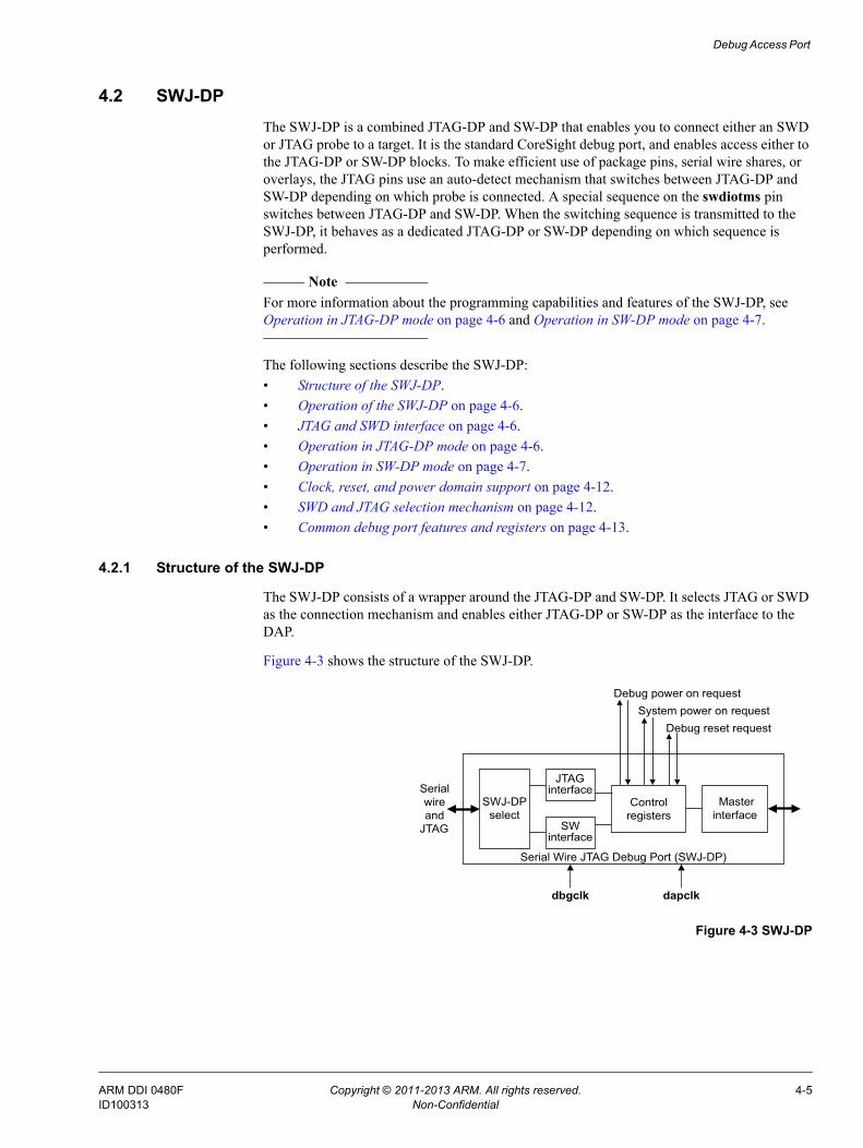
Debug Access Port
4.2 SWJ-DPThe SWJ-DP is a combined JTAG-DP and SW-DP that enables you to connect either an SWD or JTAG probe to a target. It is the standard CoreSight debug port, and enables access either to the JTAG-DP or SW-DP blocks. To make efficient use of package pins, serial wire shares, or overlays, the JTAG pins use an auto-detect mechanism that switches between JTAG-DP and SW-DP depending on which probe is connected. A special sequence on the swdiotms pin switches between JTAG-DP and SW-DP. When the switching sequence is transmitted to the SWJ-DP, it behaves as a dedicated JTAG-DP or SW-DP depending on which sequence is performed.
Note For more information about the programming capabilities and features of the SWJ-DP, see Operation in JTAG-DP mode on page 4-6 and Operation in SW-DP mode on page 4-7.
The following sections describe the SWJ-DP:• Structure of the SWJ-DP.• Operation of the SWJ-DP on page 4-6.• JTAG and SWD interface on page 4-6.• Operation in JTAG-DP mode on page 4-6.• Operation in SW-DP mode on page 4-7.• Clock, reset, and power domain support on page 4-12.• SWD and JTAG selection mechanism on page 4-12.• Common debug port features and registers on page 4-13.
4.2.1 Structure of the SWJ-DP
The SWJ-DP consists of a wrapper around the JTAG-DP and SW-DP. It selects JTAG or SWD as the connection mechanism and enables either JTAG-DP or SW-DP as the interface to the DAP.
Figure 4-3 shows the structure of the SWJ-DP.
Figure 4-3 SWJ-DP
Serial Wire JTAG Debug Port (SWJ-DP)
Controlregisters
Masterinterface
Debug power on requestSystem power on request
Debug reset request
JTAGinterface
SWinterface
Serial wire and
JTAG
SWJ-DP select
dapclkdbgclk
ARM DDI 0480F Copyright © 2011-2013 ARM. All rights reserved. 4-5ID100313 Non-Confidential

Debug Access Port
4.2.2 Operation of the SWJ-DP
SWJ-DP enables you to design an Application Specific Integrated Circuit (ASIC) that you can use in systems that require either a JTAG interface or an SWD interface. There is a trade-off between the number of pins used and compatibility with existing hardware and test devices. There are several scenarios where you must use a JTAG debug interface. These enable:
• Inclusion in an existing scan chain, usually on-chip TAPs used for test or other purposes.
• The device to be cascaded with legacy devices that use JTAG for debug.
• Use of existing debug hardware with the corresponding test TAPs, for example in Automatic Test Equipment (ATE).
You can connect an ASIC that has the SWJ-DP support to legacy JTAG devices without making any changes. If an SWD tool is available, only two pins are required, instead of the usual four pins used for JTAG. You can therefore use the other two pins for other purposes.
You can only use these two pins if there is no conflict with their use in JTAG mode. To support use of SWJ-DP in a scan chain with other JTAG devices, the default state after reset must be to use these pins for their JTAG function. If the direction of the alternative function is compatible with being driven by a JTAG debug device, the transition to a shift state can be used to transition from the alternative function to JTAG mode. You cannot use the other function while the ASIC is in JTAG debug mode.
The switching scheme is arranged so that, provided there is no conflict on the tdi and tdo pins, a JTAG debugger can connect by sending a specific sequence. The connection sequence used for SWD is safe when applied to the JTAG interface, even if hot-plugged, enabling the debugger to continually retry its access sequence. A sequence with tms=1 ensures that JTAG-DP, SW-DP, and the watcher circuit are in a known reset state. The pattern used to select SWD has no effect on JTAG targets. SWJ-DP is compatible with a free-running tck or a gated clock that external tools provide.
4.2.3 JTAG and SWD interface
The external JTAG interface has four mandatory pins, tck, tms, tdi, and tdo, and an optional reset, ntrst. JTAG-DP and SW-DP also require a separate powerup reset, npotrst.
The external SWD interface requires two pins:• A bidirectional swdio signal.• A clock, swclk, that can be input or output from the device.
The block level interface has two pins for data and an output enable that must be used to drive a bidirectional pad for the external interface, and clock and reset signals. To enable sharing of the connector for either JTAG or SWD, connections must be made external to the SWJ-DP block. In particular, tms must be a bidirectional pin to support the bidirectional swdio pin in SWD mode.
4.2.4 Operation in JTAG-DP mode
When operating as a JTAG-DP this follows the JTAG-DP as defined in the ARM® Debug Interface Architecture Specification, ADIv5.0 to ADIv5.2. It also contains an explanation of its programmers model, capabilities, and features.
The JTAG-DP contains a debug port state machine that controls the JTAG-DP mode operation, including controlling the scan chain interface that provides the external physical interface to the JTAG-DP. It is based closely on the JTAG TAP State Machine. See IEEE Std 1149.1-2001.
ARM DDI 0480F Copyright © 2011-2013 ARM. All rights reserved. 4-6ID100313 Non-Confidential
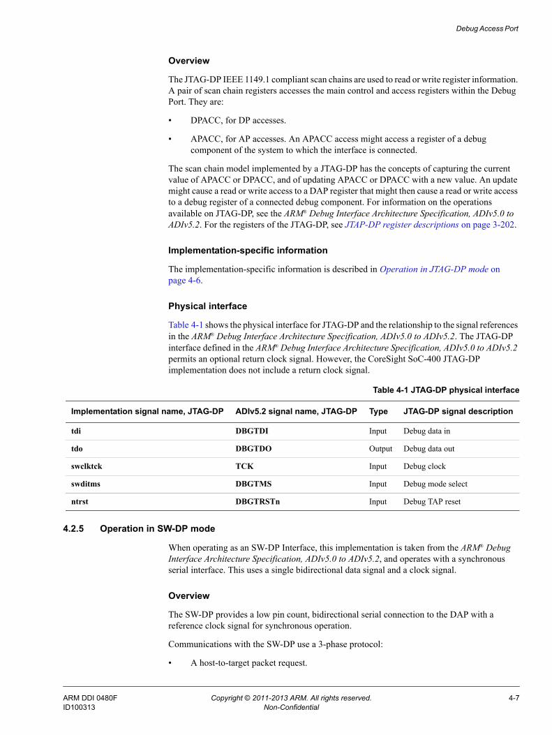
Debug Access Port
Overview
The JTAG-DP IEEE 1149.1 compliant scan chains are used to read or write register information. A pair of scan chain registers accesses the main control and access registers within the Debug Port. They are:
• DPACC, for DP accesses.
• APACC, for AP accesses. An APACC access might access a register of a debug component of the system to which the interface is connected.
The scan chain model implemented by a JTAG-DP has the concepts of capturing the current value of APACC or DPACC, and of updating APACC or DPACC with a new value. An update might cause a read or write access to a DAP register that might then cause a read or write access to a debug register of a connected debug component. For information on the operations available on JTAG-DP, see the ARM® Debug Interface Architecture Specification, ADIv5.0 to ADIv5.2. For the registers of the JTAG-DP, see JTAP-DP register descriptions on page 3-202.
Implementation-specific information
The implementation-specific information is described in Operation in JTAG-DP mode on page 4-6.
Physical interface
Table 4-1 shows the physical interface for JTAG-DP and the relationship to the signal references in the ARM® Debug Interface Architecture Specification, ADIv5.0 to ADIv5.2. The JTAG-DP interface defined in the ARM® Debug Interface Architecture Specification, ADIv5.0 to ADIv5.2 permits an optional return clock signal. However, the CoreSight SoC-400 JTAG-DP implementation does not include a return clock signal.
4.2.5 Operation in SW-DP mode
When operating as an SW-DP Interface, this implementation is taken from the ARM® Debug Interface Architecture Specification, ADIv5.0 to ADIv5.2, and operates with a synchronous serial interface. This uses a single bidirectional data signal and a clock signal.
Overview
The SW-DP provides a low pin count, bidirectional serial connection to the DAP with a reference clock signal for synchronous operation.
Communications with the SW-DP use a 3-phase protocol:
• A host-to-target packet request.
Table 4-1 JTAG-DP physical interface
Implementation signal name, JTAG-DP ADIv5.2 signal name, JTAG-DP Type JTAG-DP signal description
tdi DBGTDI Input Debug data in
tdo DBGTDO Output Debug data out
swclktck TCK Input Debug clock
swditms DBGTMS Input Debug mode select
ntrst DBGTRSTn Input Debug TAP reset
ARM DDI 0480F Copyright © 2011-2013 ARM. All rights reserved. 4-7ID100313 Non-Confidential
Debug Access Port
• A target-to-host acknowledge response.
• A data transfer phase, if required. This can be target-to-host or host-to-target, depending on the request made in the first phase.
A packet request from a debugger indicates whether the required access is to a DP register, DPACC, or to an AP register, APACC, and includes a 2-bit register address. See the ARM® Debug Interface Architecture Specification, ADIv5.0 to ADIv5.2
Implementation-specific information
This section contains the following:• Clocking.• Overview of debug interface.
Clocking
The SW-DP clock, swclktck, can be asynchronous to the dapclk. swclktck can be stopped when the debug port is idle.
The host must continue to clock the interface for a number of cycles after the data phase of any data transfer. This ensures that the transfer can be clocked through the SW-DP. This means that after the data phase of any transfer the host must do one of the following:
• Immediately start a new SW-DP operation.
• Continue to clock the SW-DP serial interface until the host starts a new SW-DP operation.
• After clocking out the data parity bit, continue to clock the SW-DP serial interface until it has clocked out at least eight more clock rising edges, before stopping the clock.
Overview of debug interface
This section describes the physical interface that the SW-DP uses.
Line interface The SW-DP uses a serial wire for both host and target sourced signals. The host emulator drives the protocol timing, that is, only the host emulator generates packet headers.The SW-DP operates in synchronous mode, and requires a clock pin and a data pin.Synchronous mode uses a clock reference signal that can be sourced from an on-chip source and exported, or provided by the host device. The host uses this clock as a reference for generation and sampling of data so that the target is not required to perform any over-sampling.Both the target and host are capable of driving the bus HIGH and LOW, or tri-stating it. The ports must be able to tolerate short periods of contention so that it can handle loss of synchronization.
Line pull-up Both the host and target are able to drive the line HIGH or LOW, so it is important to ensure that contention does not occur by providing undriven time slots as part of the hand-over. So that the line can be assumed to be in a known state when neither host nor target is driving the line, a 100kΩ pull-up is required at the target, but this can only be relied on to maintain the state of the wire. If the wire is tied LOW and released, the pull-up resistor eventually brings the line to the HIGH state, but this takes many bit periods.
ARM DDI 0480F Copyright © 2011-2013 ARM. All rights reserved. 4-8ID100313 Non-Confidential

Debug Access Port
The pull-up is intended to prevent false detection of signals when no host device is connected. It must be of a high value to reduce IDLE state current consumption from the target when the host actively pulls down the line.
Note Whenever the line is tied LOW, this results in a small current drain from the
target. If the interface is left connected over an extended period with the target in low-power mode, the host must hold the line HIGH until the interface is re-activated.
Line turn-round To avoid contention, a turnaround period is required whenever the device driving the wire changes.
Idle and reset Between transfers, the host must either drive the line LOW to the IDLE state, or continue immediately with the start bit of a new transfer. The host is also free to leave the line HIGH, either driven or tri-stated, after a packet. This reduces the static current drain, but if this approach is used with a free running clock, a minimum of 50 clock cycles must be used, followed by a read ID request that initiates a new reconnection sequence.There is no explicit reset signal for the protocol. A reset is detected by either host or target when the expected protocol is not observed. It is important that both ends of the link are reset restarting the reconnection sequence that restarts use of the protocol. Resynchronization following the detection of protocol errors or after reset is achieved by providing 50 clock cycles with the line HIGH, or tri-state, followed by a read ID request.If the SW-DP detects that it has lost synchronization, for example, if no stop bit is seen when expected, it leaves the line undriven and waits for the host to either re-try with a new header after a minimum of one cycle with the line LOW, or signals a reset by not driving the line itself. If the SW-DP detects two bad data sequences in a row, it locks out until a reset sequence of 50 clock cycles with DBGDI HIGH is seen.If the host does not see an expected response from SW-DP, it must allow time for SW-DP to return a data payload. The host can then retry with a read to the SW-DP ID code register. If this is unsuccessful, the host must attempt a reset.
Transfer timings
This section describes the interaction between the timing of transactions on the serial wire interface, and the DAP internal bus transfers. The section describes when the target responds with a WAIT acknowledgement.
Access port accesses result in the generation of transfers on the DAP internal bus. These transfers have an address phase and a data phase. The data phase can be extended by the access if it requires extra time to process the transaction, for example, if it must perform an AHB access to the system bus to read data.
ARM DDI 0480F Copyright © 2011-2013 ARM. All rights reserved. 4-9ID100313 Non-Confidential
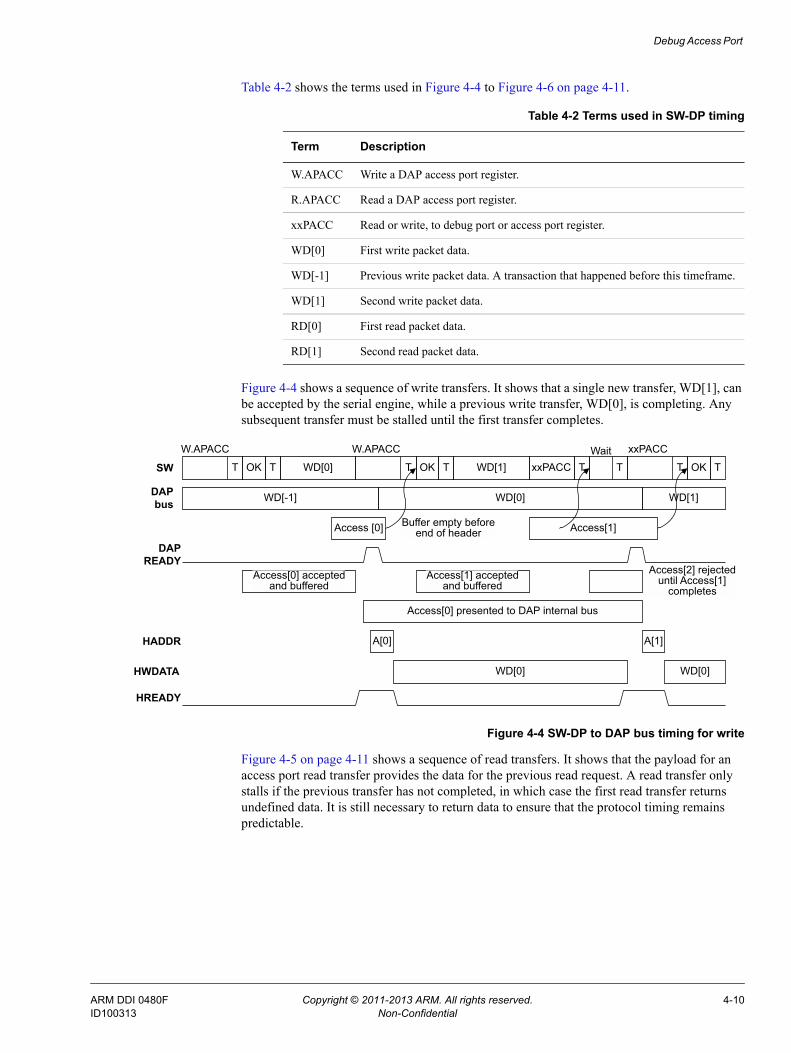
Debug Access Port
Table 4-2 shows the terms used in Figure 4-4 to Figure 4-6 on page 4-11.
Figure 4-4 shows a sequence of write transfers. It shows that a single new transfer, WD[1], can be accepted by the serial engine, while a previous write transfer, WD[0], is completing. Any subsequent transfer must be stalled until the first transfer completes.
Figure 4-4 SW-DP to DAP bus timing for write
Figure 4-5 on page 4-11 shows a sequence of read transfers. It shows that the payload for an access port read transfer provides the data for the previous read request. A read transfer only stalls if the previous transfer has not completed, in which case the first read transfer returns undefined data. It is still necessary to return data to ensure that the protocol timing remains predictable.
Table 4-2 Terms used in SW-DP timing
Term Description
W.APACC Write a DAP access port register.
R.APACC Read a DAP access port register.
xxPACC Read or write, to debug port or access port register.
WD[0] First write packet data.
WD[-1] Previous write packet data. A transaction that happened before this timeframe.
WD[1] Second write packet data.
RD[0] First read packet data.
RD[1] Second read packet data.
T OK T WD[0] T OK T WD[1] xxPACC T T T OK TSW
WD[-1] WD[0] WD[1]
Access [0] Access[1]
Access[0] accepted and buffered
Access[1] accepted and buffered
Access[2] rejected until Access[1]
completes
Access[0] presented to DAP internal bus
A[0] A[1]
WD[0] WD[0]
Buffer empty before end of header
DAP bus
DAP READY
HADDR
HWDATA
HREADY
W.APACC W.APACC Wait xxPACC
ARM DDI 0480F Copyright © 2011-2013 ARM. All rights reserved. 4-10ID100313 Non-Confidential

Debug Access Port
Figure 4-5 SW-DP to DAP bus timing for read
Figure 4-6 shows a sequence of transfers separated by IDLE periods. It shows that the wire is always handed back to the host after a transfer.
Figure 4-6 SW-DP idle timing
After the last bit in a packet, the line can be LOW, or Idle, for any period longer than a single bit, to enable the Start bit to be detected for back-to-back transactions.
SW-DP multi-drop support
The SW-DP implements the multi-drop extensions defined as part of Serial Wire protocol version 2 in the ARM® Debug Interface Architecture Specification, ADIv5.0 to ADIv5.2. This enables multiple SW-DP implementations supporting multi-drop extensions to share a single target connection.
The multi-drop extensions are fully backwards compatible. All targets are selected following a Wire Reset, and remain selected unless a TARGETSEL command is received that selects a single target.
Each target must be configured with a unique combination of target ID and instance ID, to enable a debugger to select a single target to communicate with:
• The target ID is a 32-bit field that uniquely identifies the system accessed by the SW-DP.
• The instance ID is a 4-bit field that distinguishes between multiple instances of the same target in a system. For example, because the same chip is used more than once on a board.
The multi-drop extensions do not enable the target ID and instance ID of targets to be read when multiple targets share a connection. The debugger must either be programmed with the target ID and instance ID of each target in advance, or must iterate through a list of known target IDs and instance IDs to discover which targets are connected.
T OK RD[-1] T OK RD[0] xxPACC T T xxPACC T OK TSW
RD[0] RD[1]
A[0] A[1]
RD[0] RD[1]
DAP bus
DAP READY
HADDR
HWDATA
HREADY
T
RD[0] RD[0]DP read buffer
R.APACC[0] R.APACC[1] Wait
T OK T WDATA T OK RDATA T xxPACC T T
W.APACC R.APACC Wait
ARM DDI 0480F Copyright © 2011-2013 ARM. All rights reserved. 4-11ID100313 Non-Confidential
Debug Access Port
Target ID
The SW-DP target ID is configured using a 32-bit input to the SW-DP, targetid[31:0]. Table 4-3 shows how it must be connected.
The target ID must be configured even in systems where multi-drop operation is not required, because it can be used for part identification. For more information on how to define the target ID, see the ARM® CoreSight™ SoC-400 System Design Guide.
Instance ID
The SW-DP instance ID is configured using a 4-bit input to the SW-DP, instanceid[3:0]. If multiple targets with the same target ID might share a connection, instanceid must be driven differently for each target, for example by using non-volatile storage configured differently for each target. In most cases, you can tie this input as LOW.
4.2.6 Clock, reset, and power domain support
In the swclktck clock domain, there are registers to enable power control for the on-chip debug infrastructure. This enables the majority of the debug logic, for example, trace link components such as funnel, and trace sink components such as ETR, to be powered down by default. In this situation, only the serial engine must be clocked. A debug session then starts by powering up the debug sub-system. Optionally, the debugger can write to registers in the cxgpr, if present within the debug sub-system, to power up debug components selectively. In SWJ-DP, either JTAG-DP or SW-DP can make power up or reset requests but only if they are the selected device. Even in a system that does not provide a clock and reset control interface to the DAP, it is necessary to connect these signals so that it appears that a clock and reset controller is present. This permits correct handshaking of the request and acknowledge signals.
The SWJDP must be placed in an always-on domain. By instantiating an asynchronous DAPBUS bridge on the DAPBUS output of the SWJDP, the SWJDP can be power-isolated from the Debug domain.
4.2.7 SWD and JTAG selection mechanism
SWJ-DP enables one of the following modes to be selected:• JTAG protocol.• Serial Wire Debug protocol.• Dormant.
When in dormant mode, the tms, tdi, and tdo signals can be used for other purposes, enabling other devices connected to the same pins to use alternative debug protocols.
Table 4-3 TARGETID input connections
Bits Name Description
[31:28] Revision The revision of the part. This field is not used when selecting a target.
[27:12] Part number Identifies the part.
[11:1] Designer Identifies the designer of the part. The code used is assigned by JEDEC standard JEP-106 as used in IEEE 1149.1 and CoreSight identification registers. Bits[11:8] identify the bank, and bits[7:1] identify the position within that bank.
[0] Reserved Must be HIGH.
ARM DDI 0480F Copyright © 2011-2013 ARM. All rights reserved. 4-12ID100313 Non-Confidential
Debug Access Port
The switcher defaults to JTAG operation on power up reset. Therefore the JTAG protocol can be used from reset without sending a selection sequence.
The SWJ-DP contains a mode status output, jtagnsw, that is HIGH when the SWJ-DP is in JTAG mode and LOW when in SWD or Dormant mode. This signal can be used to:
• Disable other TAP controllers when the SWJ-DP is in SWD or dormant mode, for example by disabling tck or forcing tms HIGH.
• Multiplex the SWO, traceswo, onto another pin such as tdo when not in JTAG mode.
Another status output, jtagtop, indicates the state of the JTAG-DP TAP controller. The states are:• Test-Logic-Reset.• Run-Test/Idle.• Select-DR-Scan.• Select-IR-Scan.
This signal can be used with jtagnsw to control multiplexers so that, for example, tdo and tdi can be reused as General Purpose Input/Output (GPIO) signals when the device is not in JTAG mode, or during cycles when these signals are not in use by the JTAG-DP TAP controller.
See the ARM® Debug Interface Architecture Specification, ADIv5.0 to ADIv5.2 for information on the SWJ-DP switching sequences.
4.2.8 Common debug port features and registers
This section describes specific information about features and registers that are present in this implementation of SW-DP and JTAG-DP as part of the SWJ-DP. See the ARM® Debug Interface Architecture Specification, ADIv5.0 to ADIv5.2.
This section contains the following:• Features overview.• Example pushed operations on page 4-14.
Features overview
Both the SW-DP and JTAG-DP views within the SWJ-DP contain the same features as those that are defined in the ARM® Debug Interface Architecture Specification, ADIv5.0 to ADIv5.2. The following features are included:
• Sticky flags and debug port error responses as a result of either a read and write error response from the system or because of an overrun detection, STICKYORUN.
• Pushed compare and pushed verify to enable more optimized control from a debugger by performing a set of write transactions and enabling any comparison operation to be done within the debug port. See Example pushed operations on page 4-14.
• Transaction counter to recover to a point within a repeated operation.
• System and debug power and debug reset control. This is to enable an external debugger to connect to a potentially turned-off system and to power up as much as is required to get a basic level of debug access with minimal understanding of the system.
For more information, see the ARM® Debug Interface Architecture Specification, ADIv5.0 to ADIv5.2
ARM DDI 0480F Copyright © 2011-2013 ARM. All rights reserved. 4-13ID100313 Non-Confidential
Debug Access Port
Example pushed operations
These are two examples that use this specific implementation of the ARM® Debug Interface Architecture Specification, ADIv5.0 to ADIv5.2. All register and feature references relate to this specification.
This section contains the following examples:• Example use of pushed verify operation on an AHB-AP.• Example use of pushed find operation on an AHB-AP.
Example use of pushed verify operation on an AHB-AP
You can use pushed verify to verify the contents of system memory as follows:
1. Make sure that the AHB-AP Control/Status Word (CSW) is set up to increment the Transfer Address Register (TAR) after each access.
2. Write to the TAR to indicate the start address of the Debug Register region that is to be verified.
3. Write a series of expected values as access port transactions. On each write transaction, the debug port issues an access port read access, compares the result against the value from the access port write transaction, and sets the STICKYCMP bit in the CTRL/STAT Register if the values do not match. The TAR is incremented on each transaction.
In this way, the series of values is compared against the contents of the access port locations and STICKYCMP is set if they do not match.
Example use of pushed find operation on an AHB-AP
You can use pushed find to search system memory for a particular word. If you use pushed find with byte lane masking you can search for one or more bytes.
1. Make sure that the AHB-AP CSW is set up to increment the TAR after each access.
2. Write to the TAR to indicate the start address of the Debug Register region that is to be searched.
3. Write the value to be searched for as an AP write transaction. The debug port repeatedly reads the location indicated by the TAR. On each debug port read:• The value returned is compared with the value from the access port write
transaction. If they match, the STICKYCMP flag is set.• The TAR is incremented.
This continues until STICKYCMP is set or you terminate the search using ABORT.
You can also use pushed find without address incrementing to poll a single location, for example, to test for a flag being set on completion of an operation.
ARM DDI 0480F Copyright © 2011-2013 ARM. All rights reserved. 4-14ID100313 Non-Confidential

Debug Access Port
4.3 DAPBUS interconnect The DAPBUS interconnect is a combinational component for connecting the DP to the APs in the DAP.
4.3.1 Clock and reset
There are no clock or reset pins because this component is a combinational block.
4.3.2 Functional interfaces
The DAPBUS interconnect has one DAPBUS slave interface. It has a configurable number of DAPBUS master interfaces. This is defined at design time.
4.3.3 Operation
To address a particular AP, the DP uses the eight MSBs of its address bus, dapcaddrs[15:2]. The value driven on these address lines is determined by the APSEL[7:0] field in the AP Select register. This register is present on all DP implementations that are compliant with the ARM® Debug Interface Architecture Specification, ADIv5.0 to ADIv5.2.
An access to a master interface that does not exist goes to the default slave, which ignores writes and returns zero on reads.
ARM DDI 0480F Copyright © 2011-2013 ARM. All rights reserved. 4-15ID100313 Non-Confidential

Debug Access Port
4.4 DAPBUS asynchronous bridgeThe DAPBUS asynchronous bridge enables data transfer between two asynchronous clock domains. It also provides an optional LPI to support its use between two power domains.
4.4.1 Clock and reset
The clocks and resets of the DAPBUS asynchronous bridge are:
dapclkm Clock for the master interface.
dapclks Clock for the slave interface.
dapclkenm Clock enable for the master interface.
dapclkens Clock enable for the slave interface.
dapresetmn Active-LOW reset for the master interface. This is asynchronously asserted and must be synchronously deasserted.
dapresetsn Active-LOW reset for the slave interface. This is asynchronously asserted and must be synchronously deasserted.
4.4.2 Functional interfaces
The DAPBUS asynchronous bridge has the following interfaces:• One DAPBUS master interface.• One DAPBUS slave interface.• One optional LPI slave interface.
4.4.3 Functional description
The DAPBUS asynchronous bridge carries one transaction at a time across the clock domain boundary.
Aborting the current transaction The SWJ-DP can abort a transaction in progress by driving dapaborts to HIGH. The bridge responds to the abort by driving dapreadys HIGH, ending the current transaction. However, the next transaction is stalled until the previously aborted transaction completes on the master interface.
4.4.4 Low-power features
The DAPBUS asynchronous bridge supports an optional LPI to a power controller. The power controller can request the master interface of the bridge to go into low-power state through the LPI. The bridge enters low-power state when there are no pending transactions.
When the bridge is in low-power mode and it receives a new transaction, it generates a wake-up request on the LPI by driving cactive HIGH and issues the transaction through its master interface when the power controller brings the master interface out of low-power state. The bridge stalls the transaction on the slave interface until the master interface is brought out of low-power state, and ensures that there is no loss of data transferred through the bridge.
ARM DDI 0480F Copyright © 2011-2013 ARM. All rights reserved. 4-16ID100313 Non-Confidential

Debug Access Port
4.5 DAPBUS synchronous bridgeThe DAPBUS synchronous bridge enables data transfer between two synchronous clock domains. It can be used as a register slice within a clock domain to break long timing paths. It also includes an optional LPI to support its use between two power domains.
4.5.1 Clock and reset
The two synchronous clock domains must use the same clock input. Clock enable inputs are used to indicate the relative speeds of the two clock domains. The clocks and resets of the DAPBUS synchronous bridge are:
dapclk Clock.
dapresetn Active-LOW reset. This is asynchronously asserted and must be synchronously deasserted.
dapclkens Clock enable for the slave interface.
dapclkenm Clock enable for the master interface.
4.5.2 Functional interface
The DAPBUS synchronous bridge has the following interfaces:• One DAPBUS master interface.• One DAPBUS slave interface.• One optional LPI slave interface.
4.5.3 Functional description
The DAPBUS synchronous bridge carries one transaction at a time.
The bridge can be used as a register slice to aid timing closure.
Special considerations apply when using the clock enable inputs to interface between synchronous clock domains. For more information, see the ARM® CoreSight™ SoC-400 Integration Manual.
4.5.4 Low power features
The DAPBUS synchronous bridge LPI interface functions in the same way as the DAPBUS asynchronous bridge LPI interface. See Chapter 5 APB Interconnect Components.
ARM DDI 0480F Copyright © 2011-2013 ARM. All rights reserved. 4-17ID100313 Non-Confidential

Debug Access Port
4.6 JTAG-APThe JTAG-AP provides JTAG access to on-chip components, operating as a JTAG master port to drive JTAG chains throughout a SoC. The JTAG command protocol is byte-oriented, with a word wrapper on the read and write ports to yield acceptable performance from the 32-bit internal data bus in the DAP. Daisy chaining is avoided by using a port multiplexer. In this way, slower cores do not impede faster cores. See the ARM® Debug Interface Architecture Specification, ADIv5.0 to ADIv5.2.
The implementation-specific features of the JTAG-AP are described in the following sections:• External interfaces.• RTCK connections.
4.6.1 External interfaces
Table 4-4 shows the JTAG to slave device signals.
Each of the eight JTAG scan chains is on the same bit position for each JTAG signal. For example, connections for scan chain 0 can be located on bit [0] of each bus connection of cstck, cstms, cstdi, and portconnected.
4.6.2 RTCK connections
This section describes the rtck connections.
Global port and RTCK
When more than one bit of portsel[7:0] is set, all active JTAG-AP multiplexer port rtcks are combinatorially joined, so that:• If tck=0 then select OR of active rtcks.• If tck=1 then select AND of active rtcks.
An active rtck is generated by an active port that is defined as a port which:• Is selected, when its portsel[7:0] bit is set.• Is connected, when its portconnected[7:0] bit is set.
Table 4-4 JTAG to slave device signals
Name Type Description
nsrstout[7:0] Output Sub system reset out.
srstconnected[7:0] Input Sub system reset is present.
ncstrst[7:0] Output JTAG test reset.
cstck[7:0] Output JTAG test clock.
cstms[7:0] Output JTAG test mode select.
cstdi[7:0] Output JTAG test data in, to external TAP.
cstdo[7:0] Input JTAG test data out, from external TAP.
csrtck[7:0] Input Return test clock, target pacing signal.
portconnected[7:0] Input JTAG port is connected, status signal.
portenabled[7:0] Input JTAG port is enabled, for example, it might be deasserted by a processor powering down.
ARM DDI 0480F Copyright © 2011-2013 ARM. All rights reserved. 4-18ID100313 Non-Confidential
Debug Access Port
• Has not been disabled or powered down in this session, when its PSTA bit is 0.
If no ports are active, rtck is connected directly to tck. This means that disabling or powering down a JTAG slave cannot lock up the rtck interface.
Asynchronous TAP controllers that do not require an rtck connection must connect their tck output from JTAG-AP to the corresponding rtck input.
RTCK wrapper
Note This section applies only to synchronous TAP controllers.
Where devices do not have a return clock, an rtck wrapper must be used to register tck against the processor clock. See Additional reading on page ix and the applicable Integration Manual for information on how to implement an rtck wrapper.
ARM DDI 0480F Copyright © 2011-2013 ARM. All rights reserved. 4-19ID100313 Non-Confidential

Debug Access Port
4.7 AXI-APThe AXI-AP implements the MEM-AP architecture to directly connect to an AXI memory system. You can connect it to other memory systems using a suitable bridging component.
For more information on the key features and the configuration options of the AXI-AP, see Additional reading on page ix.
4.7.1 Clock and reset
The AXI-AP operates in a single clock domain, which must be used for both the DAPBUS interface and the AXI interface. The clock and reset signals of the AHB-AP are:
clk Clock
resetn Active-LOW reset. This is asynchronously asserted and must be synchronously deasserted.
On AXI-AP reset, the entire AXI-AP module is reset and the transaction history is lost. ARM recommends that reset is not asserted while an AXI transfer is in progress. However, AXI-AP permits reset to be asserted with the understanding that all transaction history is lost.
4.7.2 Functional interfaces
AXI-AP has the following bus interfaces:• DAPBUS slave interface that connects to the DAPBUS interconnect.• Authentication slave interface.• AXI4 master interface.
4.7.3 AXI-AP features
Table 4-5 shows the features implemented by AXI-AP.
Table 4-5 AXI-AP features
Feature Comment
AXI4 interface support -
Auto-incrementing TAR -
Stalling accesses -
Access size 8, 16, 32, or 64 bits.
Endianness Little-endian.
Error response -
Packed transfers -
ROM table pointer register -
Long address support -
ARM DDI 0480F Copyright © 2011-2013 ARM. All rights reserved. 4-20ID100313 Non-Confidential

Debug Access Port
4.7.4 DAP transfer abort
If the DP issues an abort over the DAPBUS interface, abort the AXI-AP completes the transaction on its DAPBUS slave interface immediately. The DAP transfer abort does not cancel the ongoing AXI transfer.
4.7.5 Error responses
This section describes the following:• AXI initiated error responses.• AP initiated error response on page 4-22.• AXI and AP initiated error responses on page 4-22.• AXI transfers on page 4-23.• Packed transfers on page 4-24.
AXI initiated error responses
An error response received on the AXI master interface propagates onto the DAP bus as the transfer is completed.
For 64-bit data transfer, a sequence of two reads or writes must be generated on the DAP bus for a single 64-bit access on the AXI interface. For reads, the first read request on the DAP bus sends a read request on the AXI interface while for writes, a write access is sent on the AXI interface only after two write requests are received on the DAP bus.
Therefore, an error response received for a read request is for the first read request on the DAP bus while an error response received for a write request is for the second write request on the DAP bus.
AXI transfers Write, read transfers.
Burst size of 1 only.
No out-of-order transactions.
No multiple outstanding accesses.
Only aligned transfers are supported.
ACE-Lite Limited set of commands to support coherency in the system.
All transactions to non-shareable memory regions.
Limited subset of transactions to shareable memory regions.
For reads only. Supports the ReadOnce transaction type.
For writes only. Supports the WriteUnique transaction type.
Barrier transactions
Table 4-5 AXI-AP features (continued)
Feature Comment
ARM DDI 0480F Copyright © 2011-2013 ARM. All rights reserved. 4-21ID100313 Non-Confidential
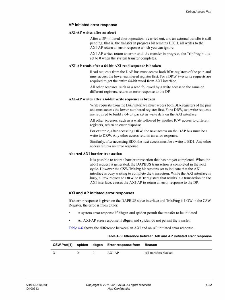
Debug Access Port
AP initiated error response
AXI-AP writes after an abort After a DP-initiated abort operation is carried out, and an external transfer is still pending, that is, the transfer in progress bit remains HIGH, all writes to the AXI-AP return an error response which you can ignore.AXI-AP writes return an error until the transfer in progress, the TrInProg bit, is set to 0 when the system transfer completes.
AXI-AP reads after a 64-bit AXI read sequence is broken Read requests from the DAP bus must access both BDx registers of the pair, and must access the lower-numbered register first. For a DRW, two write requests are required to get the entire 64-bit word from AXI interface.All other accesses, such as a read followed by a write access to the same or different registers, return an error response to the DP.
AXI-AP writes after a 64-bit write sequence is broken Write requests from the DAP interface must access both BDx registers of the pair and must access the lower-numbered register first. For a DRW, two write requests are required to build a 64-bit packet as write data on the AXI interface.All other accesses, such as a write followed by another R/W access to different registers, return an error response. For example, after accessing DRW, the next access on the DAP bus must be a write to DRW. Any other access returns an error response.Similarly, after accessing BD0, the next access must be a write to BD1. Any other access returns an error response.
Aborted AXI barrier transaction It is possible to abort a barrier transaction that has not yet completed. When the abort request is generated, the DAPBUS transaction is completed in the next cycle. However the CSW.TrInPrg bit remains set to indicate that the AXI interface is busy waiting to complete the transaction. While the AXI interface is busy, a R/W request to DRW or BDx registers that results in a transaction on the AXI interface, causes the AXI-AP to return an error response to the DP.
AXI and AP initiated error responses
If an error response is given on the DAPBUS slave interface and TrInProg is LOW in the CSW Register, the error is from either:
• A system error response if dbgen and spiden permit the transfer to be initiated.
• An AXI-AP error response if dbgen and spiden do not permit the transfer.
Table 4-6 shows the difference between an AXI and an AP initiated error response.
Table 4-6 Difference between AXI and AP initiated error response
CSW.Prot[1] spiden dbgen Error response from Reason
X X 0 AXI-AP All transfers blocked
ARM DDI 0480F Copyright © 2011-2013 ARM. All rights reserved. 4-22ID100313 Non-Confidential
Debug Access Port
If an error response is given and TrInProg is HIGH, then the error is from an access port error response. This case can only occur after the initiation of an abort when the system transfer has not completed.
AXI transfers
The AMBA4 AXI compliant Master Port supports the following features:• Bursts of single transfer.• Master processes one transaction at a time in the order they are issued.• No out-of-order transactions.• No issuing of multiple outstanding addresses.
Burst length The AXI-AP supports burst length of one transfer only. ARLEN[3:0] and AWLEN[3:0] are always 0b0000.Packed 8 or 16-bit transfers are treated as individual burst lengths of one transfer at the AXI interface. This ensures that there are no issues with boundary wrapping to avoid additional AXI-AP complexity.
Burst size Supported burst sizes are:• 8-bit.• 16-bit.• 32-bit.• 64-bit.
Burst type ARBURST and AWBURST signals are always 0b00.Because only bursts of one transfer are supported, burst type has no meaning in this context.
Atomic accesses AXI-AP supports normal accesses only.ARLOCK and AWLOCK signals are always 0b00.
Unaligned accesses Unaligned accesses are not supported. Depending on the size of the transfers, addresses must be aligned.• For 16-bit half word transfers:
— Base address 0x01 is aligned and AxADDR[7:0] = 0x00.— Base address 0x02 is retained and AxADDR[7:0] = 0x02.
0 0 1 AXI-AP Secure transfers blocked
0 1 1 System Secure transfer produced an error response
1 X 1 System Non secure transfer produced an error response
Table 4-6 Difference between AXI and AP initiated error response (continued)
CSW.Prot[1] spiden dbgen Error response from Reason
ARM DDI 0480F Copyright © 2011-2013 ARM. All rights reserved. 4-23ID100313 Non-Confidential

Debug Access Port
• For 32-bit word transfers:— Base address 0x01 to 0x03 is aligned and AxADDR[7:0] = 0x00.— Base address 0x04 is retained and AxADDR[7:0] = 0x04.
• For 64-bit word transfers:— Base address 0x04 is aligned and AxADDR[7:0] = 0x00.— Base address 0x08 is retained and AxADDR[7:0] = 0x08.
For example, for 16-bit transfers, addresses must be aligned to a 16-bit half-word boundary, for 32-bit word transfers, addresses must be word-aligned, and for 64-bit double word transfers, addresses must be double-word aligned.
Packed transfers
The DAPBUS interface is a 32-bit data bus. However, 8-bit or 16-bit transfers can be formed on AXI according to the size field in the CSW register, 0x000. The AddrInc field in the CSW Register permits optimized use of DAPBUS to reduce the number of accesses to the DAP. It indicates whether the entire data word can be used to pack more than one transfer. If packed transfers are initiated, then address incrementing is automatically enabled. Multiple transfers are carried out in sequential addresses, with the size of the address increment based on the size of the transfer.
Examples of the transactions are:
For an unpacked 16-bit write at a base address of base 0x2, that is, CSW[2:0]=0b001, CSW[5:4]=0b01, WDATA[31:16] is written from bits [31:16] in the DRW register.
For an unpacked 8-bit read at a base address of base 0x1, that is, CSW[2:0]=0b000, CSW[5:4]=0b01, RDATA[31:16] and RDATA[7:0] are zero, RDATA[15:8] contains read data.
For a packed byte write at base address of base 0x2, that is, CSW[2:0]=0b000 and CSW[5:4]=0b10, four write transfers are initiated, and the order of data that is sent is:• WDATA[23:16], from DRW[23:16] to AWADDR[31:0]=0x00000002. • WDATA[31:24], from DRW[31:24] to AWADDR[31:0]=0x00000003.• WDATA[7:0], from DRW[7:0] to AWADDR[31:0]=0x00000004.• WDATA[15:8], from DRW[15:8] to AWADDR[31:0]=0x00000005.
For a packed half-word read at a base address of base 0x2, that is, CSW[2:0]=0b001, CSW[5:4]=0b10, two read transfers are initiated:• RDATA[31:16] is stored into DRW[31:16] from ARADDR[31:0]=0x00000002.• RDATA[15:0] is stored into DRW[15:0] from ARADDR[31:0]=0x00000004.
The AXI-AP only asserts DAPREADY HIGH when all packed transfers from the AXI interface have completed.
If the current transfer is aborted or the current transfer receives an ERROR response, the AXI-AP does not complete the subsequent packed transfers and returns DAPREADY HIGH immediately after the current packed transfer.
ARM DDI 0480F Copyright © 2011-2013 ARM. All rights reserved. 4-24ID100313 Non-Confidential
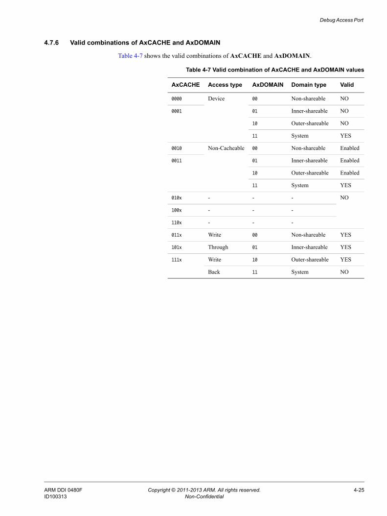
Debug Access Port
4.7.6 Valid combinations of AxCACHE and AxDOMAIN
Table 4-7 shows the valid combinations of AxCACHE and AxDOMAIN.
Table 4-7 Valid combination of AxCACHE and AxDOMAIN values
AxCACHE Access type AxDOMAIN Domain type Valid
0000 Device 00 Non-shareable NO
0001 01 Inner-shareable NO
10 Outer-shareable NO
11 System YES
0010 Non-Cacheable 00 Non-shareable Enabled
0011 01 Inner-shareable Enabled
10 Outer-shareable Enabled
11 System YES
010x - - - NO
100x - - -
110x - - -
011x Write 00 Non-shareable YES
101x Through 01 Inner-shareable YES
111x Write 10 Outer-shareable YES
Back 11 System NO
ARM DDI 0480F Copyright © 2011-2013 ARM. All rights reserved. 4-25ID100313 Non-Confidential

Debug Access Port
4.8 AHB-APThe AHB-AP implements the MEM-AP architecture to directly connect to an AHB-based memory system. Connection to other memory systems is possible through suitable bridging.
As part of the MEM-AP description, the AHB-AP has a number of implementation-specific features that are described in:• Clock and reset.• External interfaces.• Implementation features on page 4-28.• DAP transfers on page 4-28.• Differentiation between system and access port initiated error responses on page 4-29.
For information about all the registers and features in a MEM-AP, see the ARM® Debug Interface Architecture Specification, ADIv5.0 to ADIv5.2.
4.8.1 Clock and reset
The AHB-AP operates in a single clock domain, which must be used for both the DAPBUS interface and the AHB interface. The clock and reset signals of the AHB-AP are:
dapclk Clock.
dapclken Clock enable.
dapresetn Active-LOW reset. This is asynchronously asserted and must be synchronously deasserted.
The dapresetn signal must only be asserted LOW when there is no pending transaction on the AHB interface.
4.8.2 External interfaces
The primary external interface to the system is an AHB-Lite master port that supports:• AHB in AMBA v2.0.• ARM11 AMBA extensions.• TrustZone extensions.
The AHB-Lite master port does not support:• BURST and SEQ.• Exclusive accesses.• Unaligned transfers.
Table 4-8 shows the other AHB-AP ports.
Table 4-8 Other AHB-AP ports
Name Type Description
dbgen Input Enables AHB-AP transfers if HIGH. Access to the AHB-AP registers is still permitted if dbgen is LOW, but no AHB transfers are initiated. If a transfer is attempted when dbgen is LOW, then the DAP bus returns dapslverr HIGH.
spiden Input Permits secure transfers to take place on the AHB-AP. If spiden is HIGH, then hprot[6] can be asserted as programmed into the SProt bit in the CSW Register. See Chapter 3 Programmers Model.
ARM DDI 0480F Copyright © 2011-2013 ARM. All rights reserved. 4-26ID100313 Non-Confidential
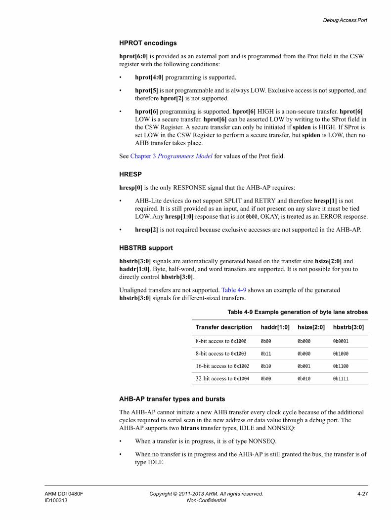
Debug Access Port
HPROT encodings
hprot[6:0] is provided as an external port and is programmed from the Prot field in the CSW register with the following conditions:
• hprot[4:0] programming is supported.
• hprot[5] is not programmable and is always LOW. Exclusive access is not supported, and therefore hprot[2] is not supported.
• hprot[6] programming is supported. hprot[6] HIGH is a non-secure transfer. hprot[6] LOW is a secure transfer. hprot[6] can be asserted LOW by writing to the SProt field in the CSW Register. A secure transfer can only be initiated if spiden is HIGH. If SProt is set LOW in the CSW Register to perform a secure transfer, but spiden is LOW, then no AHB transfer takes place.
See Chapter 3 Programmers Model for values of the Prot field.
HRESP
hresp[0] is the only RESPONSE signal that the AHB-AP requires:
• AHB-Lite devices do not support SPLIT and RETRY and therefore hresp[1] is not required. It is still provided as an input, and if not present on any slave it must be tied LOW. Any hresp[1:0] response that is not 0b00, OKAY, is treated as an ERROR response.
• hresp[2] is not required because exclusive accesses are not supported in the AHB-AP.
HBSTRB support
hbstrb[3:0] signals are automatically generated based on the transfer size hsize[2:0] and haddr[1:0]. Byte, half-word, and word transfers are supported. It is not possible for you to directly control hbstrb[3:0].
Unaligned transfers are not supported. Table 4-9 shows an example of the generated hbstrb[3:0] signals for different-sized transfers.
AHB-AP transfer types and bursts
The AHB-AP cannot initiate a new AHB transfer every clock cycle because of the additional cycles required to serial scan in the new address or data value through a debug port. The AHB-AP supports two htrans transfer types, IDLE and NONSEQ:
• When a transfer is in progress, it is of type NONSEQ.
• When no transfer is in progress and the AHB-AP is still granted the bus, the transfer is of type IDLE.
Table 4-9 Example generation of byte lane strobes
Transfer description haddr[1:0] hsize[2:0] hbstrb[3:0]
8-bit access to 0x1000 0b00 0b000 0b0001
8-bit access to 0x1003 0b11 0b000 0b1000
16-bit access to 0x1002 0b10 0b001 0b1100
32-bit access to 0x1004 0b00 0b010 0b1111
ARM DDI 0480F Copyright © 2011-2013 ARM. All rights reserved. 4-27ID100313 Non-Confidential

Debug Access Port
The only unpacked hburst encoding supported is SINGLE. Packed 8-bit transfers or 16-bit transfers are treated as individual NONSEQ, SINGLE transfers at the AHB-Lite interface. This ensures that there are no issues with boundary wrapping, to avoid additional AHB-AP complexity.
A full AHB master interface can be created by adding an AHB-Lite to AHB wrapper to the output of the AHB-AP, as provided in the AMBA Design Kit.
4.8.3 Implementation features
The AHB-AP provides the following specific MEM-AP features:
• Auto-incrementing of the Transfer Address Register with address wrapping on 1KB boundaries.
• Word, half-word, and byte accesses to devices present on the AHB memory system.
• Packed transfers on sub-word transfers.
The AHB-AP does not support the following MEM-AP features:
• Big-endian. All accesses performed as expected to be to a little-endian memory structure.
• Slave memory port disabling. The AHB-Lite master interface is not shared with any other connection so there is no slave port to disable access to this interface. If the memory-map presented to the AHB-AP is to be shared with another AHB-Lite master then this is implemented externally to the DAP.
4.8.4 DAP transfers
This section describes:• DAP transfer aborts.• Error response generation.
DAP transfer aborts
The AHB-AP does not cancel the system-facing operation and returns dapready HIGH one cycle after dapabort has been asserted by the driving debug port. The externally driving AHB master port does not violate the AHB protocol. After a transfer has been aborted, the CSW Register can be read to determine the state of the transfer in progress bit, TrInProg. When TrInProg returns to zero, either because the external transfer completes, or because of a reset, the AHB-AP returns to normal operation. All other writes to the AHB-AP are ignored until this bit is returned LOW after a transfer abort.
Error response generation
This section describes:• System initiated error response.• AHB-AP reads after an abort on page 4-29.• AHB-AP writes after an abort on page 4-29.
System initiated error response
An error response received on the system driving master propagates onto the DAP bus when the transfer is completed. This response is received by the debug ports.
ARM DDI 0480F Copyright © 2011-2013 ARM. All rights reserved. 4-28ID100313 Non-Confidential

Debug Access Port
AHB-AP reads after an abort
After a dapabort operation is carried out, and an external transfer is still pending, that is, the TrInProg bit remains HIGH, reads of all registers return a normal response except for reads of the Data R/W Register and banked registers. Reads of the Data Read/Write Register and banked registers return an error response because they cannot initiate a new system read transfer until the CSW.TrInProg is set to 0 either by completing the system transfer or by a reset.
AHB-AP writes after an abort
After a dapabort operation is carried out, and an external transfer is still pending, that is, the transfer in progress bit remains HIGH, all writes to the access port return an error response, because they are ignored until the TrInProg bit is set to 0.
4.8.5 Differentiation between system and access port initiated error responses
If dapslverr is HIGH and TrInProg is LOW in the CSW Register, the error is from either:• A system error response if dbgen and spiden permit the transfer to be initiated.• An AHB-AP error response if dbgen and spiden do not permit the transfer to be initiated.
Table 4-10 shows the error responses.
If dapslverr is HIGH and TrInProg is HIGH, then the error is from an access port error response. The transfer has not been accepted by the access port. This case can only occur after an abort has been initiated and while the system transfer has not completed.
Table 4-10 Error responses with DAPSLVERR HIGH and TrInProg LOW
SProt SPIDEN DBGEN Error response from Reason
x x 0 AHB-AP No transfers permitted
0 0 1 AHB-AP Secure transfers not permitted
0 1 1 System Secure transfer produced an error response
1 x 1 System Non secure transfer produced an error response
ARM DDI 0480F Copyright © 2011-2013 ARM. All rights reserved. 4-29ID100313 Non-Confidential

Debug Access Port
4.9 APB-APThe APB-AP implements the MEM-AP architecture to connect directly to an APB based system. This bus is normally dedicated to CoreSight and other debug components.
As part of the MEM-AP description, the APB-AP has a number of implementation-specific features. These are described in:• Clock and reset.• External interfaces.• Implementation features.• DAP transfers on page 4-31.• Authentication requirements for APB-AP on page 4-32.
For information on all the registers and features in a MEM-AP, see the ARM® Debug Interface Architecture Specification, ADIv5.0 to ADIv5.2
4.9.1 Clock and reset
The APB-AP operates in a single clock domain, which must be used for both the DAPBUS interface and the APB interface. The clock and reset signals of the APB-AP are:
dapclk Clock.
dapclken Clock enable.
dapresetn Active-LOW reset. This is asynchronously asserted and must be synchronously deasserted.
The dapresetn signal must only be asserted LOW when there is no pending transaction on the APB interface.
4.9.2 External interfaces
The primary interface on APB-AP is an APB AMBA 3 compliant interface supporting:• Extended slave transfers.• Transfer response errors.
Table 4-11 shows the other APB-AP ports.
4.9.3 Implementation features
The APB-AP provides the following specific MEM-AP features:
• Auto-incrementing of the Transfer Address Register with address wrapping on 1KB boundaries.
• Slave memory port disabling a slave interface is provided through the APB interconnect to enable another APB master to connect to the same memory-map as the APB-AP.
Table 4-11 APB-AP other ports
Name Type Description
pdbgswen Output Enables self-hosted access to the debug APB at the APB multiplexer.
deviceen Input Disables device when LOW.
ARM DDI 0480F Copyright © 2011-2013 ARM. All rights reserved. 4-30ID100313 Non-Confidential

Debug Access Port
The APB-AP does not support the following MEM-AP features:• Big-endian. All accesses must be to a little-endian memory structure.• Sub-word transfers. Only word transfers are supported.
The APB-AP has one clock domain, dapclk. It drives the complete APB-AP. This must be connected to pclkdbg for the APB interface.
dapresetn resets the internal DAP interface and the APB interface.
4.9.4 DAP transfers
This section describes DAP transfers.
Effects of DAPABORT
The APB-AP does not cancel the system-facing operation, and returns dapready HIGH one cycle after dapabort is asserted by the debug port. The externally driving APB master port does not violate the APB protocol. After a transfer is aborted, the Control and Status Register can be read to determine the state of the transfer in progress bit, TrInProg. When TrInProg returns to zero, after completing the external transfer or on a reset, the APB-AP returns to normal operation. All other writes to the APB-AP are ignored until the TrInProg bit is returned LOW after a transfer Abort.
APB-AP error response generation
APB-AP error response generation is described in:• System initiated error response.• AP-initiated error response.• Differentiation between System-initiated and AP-initiated error responses.
System initiated error response
An error response received on the APB master interface propagates onto the DAP bus when the transfer is completed. This is received by the debug ports.
AP-initiated error response
After a DP-initiated abort operation is carried out, and an external transfer is still pending, that is, the TrInProg bit in the CSW Register remains HIGH:
• Reads of all registers return a normal response except for reads of the Data Read/Write Register and banked registers. Reads of the Data Read/Write Register and banked registers return an error response because they cannot initiate a new system read transfer until CSW.TrInProg is set to 0 either by completing the system transfer or by a reset
• Writes to the access port return an error response, because they are ignored until the TrInProg bit has been set to 0.
Differentiation between System-initiated and AP-initiated error responses
If dapslverr is HIGH and TrInProg is LOW, then the error is from a system error response.
If dapslverr is HIGH and TrInProg is HIGH, then the error is from an access port error response. The transfer has not been accepted by the access port. This case can occur after an abort has been initiated and while the system transfer has not completed.
ARM DDI 0480F Copyright © 2011-2013 ARM. All rights reserved. 4-31ID100313 Non-Confidential

Debug Access Port
4.9.5 Authentication requirements for APB-AP
APB-AP has one authentication signal, called deviceen:
• If the APB-AP is connected to a debug bus, deviceen must be tied HIGH.
• If the APB-AP is connected to a system bus dedicated to the secure state, this signal must be connected to spiden.
• If the APB-AP is connected to a system bus dedicated to the non-secure state, this signal must be connected to dbgen.
For more information, see the ARM® CoreSight™ Architecture Specification.
ARM DDI 0480F Copyright © 2011-2013 ARM. All rights reserved. 4-32ID100313 Non-Confidential

Chapter 5 APB Interconnect Components
This chapter describes the APB interconnect components. It contains the following sections:• APB Interconnect with ROM table on page 5-2.• APB asynchronous bridge on page 5-5.• APB synchronous bridge on page 5-6.
ARM DDI 0480F Copyright © 2011-2013 ARM. All rights reserved. 5-1ID100313 Non-Confidential

APB Interconnect Components
5.1 APB Interconnect with ROM tableThe APB interconnect connects one or more APB bus masters, for example an APB-AP and an APB interface driven by an on-chip processor. APB interconnects can be cascaded, for example to split across multiple clock or power domains.
Each APB Interconnect implements a ROM table at address 0x00000000, which identifies the locations of the CoreSight components accessed through it.
The APB Interconnect implements a 32-bit data bus.
5.1.1 Clock and reset
This component has a single clock domain, clk, driven by the debug APB clock. The master and slave interfaces operate on the same clock, clk.
This component has a single reset input, resetn, that is an asynchronous active-LOW reset input.
5.1.2 Functional interfaces
The APB interconnect with the ROM table has a configurable number of AMBA 3 APB-compliant slave interfaces and AMBA 3 APB-compliant master interfaces. Each master interface can address a configurable address size, to support CoreSight components that require more than 4KB of address space.
The DbgSwEnable bit in the APB-AP can be used to prevent self-hosted, on-chip, accesses.
5.1.3 Device operation
This section describes device operation in the following subsections:• Accesses to ROM table.• Arbitration.• Error response on page 5-3.• Address width on master interfaces on page 5-3.• Address width on slave interfaces on page 5-4.
Accesses to ROM table
Accesses to addresses in the range 0x0000 - 0x0FFC are decoded to the ROM table. See the ARM® Debug Interface Architecture Specification, ADIv5.0 to ADIv5.2 for information on ROM tables.
Arbitration
The internal arbiter arbitrates between competing slave interfaces for access to debug APB as the following algorithm demonstrates:
• When a slave interface raises a request, the highest priority is given to the slave interface with the lowest instance suffix, that is, SlvIntf0 > SlvIntf1 > SlvIntf2 > … > SlvIntf(n-1). The order in which these slave interfaces raised their requests relative to each other is not used in arbitration.
• The arbitration is re-evaluated after every access.
ARM DDI 0480F Copyright © 2011-2013 ARM. All rights reserved. 5-2ID100313 Non-Confidential

APB Interconnect Components
Error response
The APB interconnect returns an error on its slave interface under any of the following conditions:
• The targeted debug APB device returns an error response.
• The address accessed by a slave interface does not decode to any debug APB device.
• A system access is attempted to a debug APB device when not permitted. This occurs when the DbgSwEnable bit in the APB-AP is cleared, and self-hosted, on-chip, accesses are attempted.
Address width on master interfaces
The width of the address bus on the master interface depends on the size of the address space allocated to that interface through bit[31] of the address bus. Bit[31] is always exported onto the master interface. Table 5-1 shows the address bus widths for each setting of size.
Table 5-1 Address bus on the master interfaces
Size of address spaceAddress bus on the master interface,where x=0 to NUM_MASTER_INTF-1
4KB paddrm<x>[11:2]
8KB paddrm<x>[12:2]
16 KB paddrm<x>[13:2]
32 KB paddrm<x>[14:2]
64 KB paddrm<x>[15:2]
128 KB paddrm<x>[16:2]
256 KB paddrm<x>[17:2]
512 KB paddrm<x>[18:2]
1 MB paddrm<x>[19:2]
2 MB paddrm<x>[20:2]
4 MB paddrm<x>[21:2]
8 MB paddrm<x>[22:2]
16 MB paddrm<x>[23:2]
32 MB paddrm<x>[24:2]
64 MB paddrm<x>[25:2]
128 MB paddrm<x>[26:2]
256 MB paddrm<x>[27:2]
512 MB paddrm<x>[28:2]
1 GB paddrm<x>[29:2]
ARM DDI 0480F Copyright © 2011-2013 ARM. All rights reserved. 5-3ID100313 Non-Confidential

APB Interconnect Components
Note <x> is the master interface number, from 0 to NUM_MASTER_INTF - 1.
Address width on slave interfaces
The address width on the APB slave interfaces depends on the total memory footprint occupied by the defined master interfaces and the 4KB footprint of the ROM Table.
ARM DDI 0480F Copyright © 2011-2013 ARM. All rights reserved. 5-4ID100313 Non-Confidential

APB Interconnect Components
5.2 APB asynchronous bridgeThe APB asynchronous bridge enables data transfer between two asynchronous clock domains. The APB asynchronous bridge is designed to exist across two power domains and provides an optional LPI.
5.2.1 Clock and reset
The clocks and resets of the APB asynchronous bridge are:
pclkm Clock for master interface.
pclkenm Clock enable for master interface.
presetmn Active-LOW reset for master interface. This is asynchronously asserted and must be synchronously deasserted.
pclks Clock for slave interface.
pclkens Clock enable for slave interface.
presetsn Active-LOW reset for slave interface. This is asynchronously asserted and must be synchronously deasserted.
5.2.2 Functional interfaces
The APB asynchronous bridge has the following interfaces:• One APB master compliant with APB3.• One APB slave compliant with APB3.• One optional LPI slave.
5.2.3 Low-power features
The APB asynchronous bridge supports an optional LPI to a power controller. The power controller can request the master interface of the bridge to go into low-power state through the LPI. The bridge enters low-power state when there are no pending transactions.
When the bridge is in low-power mode and it receives a new transaction, it generates a wake-up request on the LPI by driving cactive HIGH and issues the transaction through its master interface when the power controller brings the master interface out of low-power state. The bridge stalls the transaction on the slave interface until the master interface is brought out of low-power state, and ensures that there is no loss of data transferred through the bridge.
ARM DDI 0480F Copyright © 2011-2013 ARM. All rights reserved. 5-5ID100313 Non-Confidential
APB Interconnect Components
5.3 APB synchronous bridgeThe APB synchronous bridge enables data transfer between two synchronous clock domains.
5.3.1 Clock and reset
The APB synchronous bridge operates in a single clock domain with one asynchronous reset. The clocks and resets of the APB synchronous bridge are:
pclk Clock.
presetn Active-LOW reset. This is asynchronously asserted and must be synchronously deasserted.
pclkenm Clock enable for master interface.
pclkens Clock enable for slave interface.
5.3.2 Functional interface
The APB synchronous bridge has the following interfaces:• One APB master compliant with APB3.• One APB slave compliant with APB3.• One optional LPI port.
5.3.3 Functional description
APB synchronous bridge can be used as a register slice on the APB path.
Special considerations apply when using the clock enable inputs to interface between synchronous clock domains. For more information, see the ARM® CoreSight™ SoC-400 Integration Manual.
5.3.4 Low-power features
The APB synchronous bridge LPI functions in the same way as the APB asynchronous bridge LPI interface. See APB asynchronous bridge on page 5-5.
ARM DDI 0480F Copyright © 2011-2013 ARM. All rights reserved. 5-6ID100313 Non-Confidential

Chapter 6 ATB Interconnect Components
This chapter describes the ATB interconnect components. It contains the following sections:• ATB replicator on page 6-2.• ATB funnel on page 6-3.• ATB upsizer on page 6-6.• ATB downsizer on page 6-7.• ATB asynchronous bridge on page 6-8.• ATB synchronous bridge on page 6-10.
ARM DDI 0480F Copyright © 2011-2013 ARM. All rights reserved. 6-1ID100313 Non-Confidential

ATB Interconnect Components
6.1 ATB replicatorThe ATB replicator propagates the data from a single ATB master to two ATB slaves at the same time. If the optional APB interface is implemented, it can also separately filter the trace for each ATB master interface.
6.1.1 Clock and reset
The clock and reset signals of the ATB replicator are:
clk Clock.
resetn Active-LOW reset. This is asynchronously asserted and must be synchronously deasserted.
pclkendbg Clock enable for the optional debug APB interface.
6.1.2 Functional interfaces
The ATB replicator has a single slave ATB port, two ATB master ports, and one optional APB port.
6.1.3 Functional overview
The ATB replicator permits the connection of two trace sinks. If more than two trace sinks are required then multiple replicators can be used.
ID Filtering If the optional APB interface is implemented, the replicator can filter the trace for each ATB master interface according to the trace ID. Most trace sources use a single trace ID for their trace, and so the replicator can be programmed to control which trace sources are captured by each trace sink.After reset the replicator behavior matches the behavior of a non-programmable replicator, and no filtering is performed. The filtering settings can be changed at any time.
Trace data flow As data is received from the trace source, it is passed on to all trace sinks at the same time. The replicator does not accept more data from the trace source until all the trace sinks have accepted this data. This has the impact of reducing the throughput of the replicator to match that of the slowest trace sink.If the optional APB interface is implemented, a trace sink which supports high bandwidth trace, such as an ETB, can be enabled at the same time as a trace sink which supports only lower bandwidth trace, such as a TPIU. Higher bandwidth trace sources can be filtered out of the trace seen by the TPIU, so that it does not give backpressure to the replicator and therefore impact the trace seen by the ETB.
ARM DDI 0480F Copyright © 2011-2013 ARM. All rights reserved. 6-2ID100313 Non-Confidential

ATB Interconnect Components
6.2 ATB funnelThe ATB funnel component merges multiple ATB buses into a single ATB bus. If the optional APB interface is implemented, a debugger can also control the arbitration scheme and selectively enable the ATB slave interfaces for tracing.
6.2.1 Clock and reset
The clock and reset signals of the ATB funnel are:
clk Clock.
resetn Active-LOW reset. This is asynchronously asserted and must be synchronously deasserted.
pclkendbg Clock enable for the optional debug APB interface.
6.2.2 Functional interface
The ATB funnel has a configurable number of ATB slave interfaces and one ATB master interface. The widths of the ATB interfaces are configurable but they must be configured to be the same and to match the ATB data width.
6.2.3 ATB slave interface enable
The ATB slave interfaces can be independently enabled and disabled using the optional APB programming interface. The settings can be changed at any time.
If the APB programming interface is not implemented then all ATB slave interfaces are enabled.
6.2.4 Arbitration
The funnel implements two arbitration schemes, which can be used at the same time:• Fixed priority.• Round robin.
Priority values for each ATB slave interface are defined in a 3-bit field in the Priority Control register. Fixed priority arbitration is used between interfaces programmed with different priority values, with priority level 0 having the highest priority and priority level 7 having the lowest priority. Round robin arbitration is used between interfaces programmed with the same priority value.
At reset, all ports have a value of 0, and round robin arbitration is used between all interfaces.
A minimum hold time value can be set in the Funnel Control register, which affects both arbitration schemes. At reset, a minimum hold time of four transactions is selected.
The arbitration scheme prioritizes ATB interfaces as follows:
1. The interface that was previously selected, if it has valid trace available with the same ID as previously, and the minimum hold time has not been reached. The hold time is the number of successive times the same interface has been selected, ignoring cycles where no interfaces had valid trace.
2. Interfaces in the flush state. When a flush occurs the flush request is propagated to all slave interfaces, and those which have not yet completed the flush are given priority over those which have completed the flush.
ARM DDI 0480F Copyright © 2011-2013 ARM. All rights reserved. 6-3ID100313 Non-Confidential

ATB Interconnect Components
3. Interfaces with a higher programmed priority level. This is the fixed priority arbitration scheme.
4. Interfaces which were not previously selected. This is the round robin arbitration scheme. When an interface has been selected, it is marked as having lower priority than other interfaces with the same programmed priority level. When an interface that has already been marked is selected again, for example because all of the interfaces at that priority level have been selected in turn, the marks are cleared for other interfaces at the same programmed priority level and the scheme starts again.
5. Interfaces with a lower port number.
Minimum hold time If the funnel switches between interfaces, and therefore ATB IDs, this can frequently result in inefficiency:• The formatter in the trace sink must add extra trace to indicate the change
of ATB ID.• An upsizer placed downstream of the funnel is less efficient, because trace
with different IDs cannot be combined into a single cycle.The minimum hold time setting reduces the frequency of switching between interfaces: • If you reduce the minimum hold time then the overall bandwidth of the
trace system might be reduced, because of more frequent switching.• If you increase the minimum hold time then the FIFOs of individual trace
sources might be insufficient, leading to greater overflow.ARM recommends the default value of four transactions in most cases.
Example minimum hold time waveform Figure 6-1 shows the effect of minimum hold time for a two ATB slave port funnel programmed as follows:• Slave port priority arbitration, where slave port 0 has the higher priority,
and slave port 1 has the lower priority.• A minimum hold time of 4.
Figure 6-1 ATB funnel minimum hold time example
clk
atvalids0
atreadys0
atvalids1
atreadys1
t0 t1 t2
atvalidm
atreadym
t3
ARM DDI 0480F Copyright © 2011-2013 ARM. All rights reserved. 6-4ID100313 Non-Confidential

ATB Interconnect Components
Table 6-1 shows the sequence of events in Figure 6-1 on page 6-4.
6.2.5 Cascaded funnel support
The funnel is a combinatorial block, and when a cascaded funnel configuration is implemented, a register slice that is a forward, reverse, or full register slice must be instantiated between the cascaded funnels to avoid combinatorial timing loops.
6.2.6 Topology detection
The funnel supports topology detection through a set of integration registers that enable reading or writing atvalid and atready of all the ATB interfaces. Integration mode is enabled by setting the Integration mode bit in the ITCTRL register.
Register ITATBCTR2 is the Integration Test ATB Control 2 register. A write to ITATBCTR2 outputs data on atreadysn, where n is defined by the status of the Ctrl_Reg. A read from ITATBCTR2 returns the data from atreadym.
Register ITATBCTR0 is the Integration Test ATB Control 0 register. A write to ITATBCTR0 sets the value of atvalidm. A read from ITATBCTR0 returns the value of atvalidsn, where n is defined by the status of the Ctrl_Reg.
It is illegal to have more than one ATB slave port enabled while in integration mode and performing topology detection. No hardware protection exists and enabling multiple ports is considered to be a programming error.
After performing integration or topology detection, you must reset the system to ensure the correct behavior of CoreSight SoC-400 and other connected system components that are affected by the integration or topology detection.
6.2.7 Non-programmable funnel
In the non-programmable configuration, the funnel does not have an APB interface. The funnel behavior is equivalent to the following register settings:
• Ctrl_Reg = 0x000003FF. All ATB slave interfaces are enabled, where present, and the hold time is four transfers.
• Priority_Ctrl_Reg = 0x00000000. All slave interfaces have the same priority and the round-robin scheme is used to select between them.
• ITCTRL = 0x00000000. Integration mode is not supported and the funnel is transparent for topology detection.
Table 6-1 Event sequence
Time Event
t0 • Slave port 1 is currently selected. • Higher priority slave port 0 has a pending transfer.• Slave port 1 remains selected because the minimum hold time has not expired.
t1 • Slave port 1 remains selected because the minimum hold time has not expired.
t2 • Minimum hold time expires for slave port 1 and funnel switches to slave port 0.
t3 • Slave port 0 has no more data to transfer and the funnel switches back to slave port 1.
ARM DDI 0480F Copyright © 2011-2013 ARM. All rights reserved. 6-5ID100313 Non-Confidential

ATB Interconnect Components
6.3 ATB upsizerThe ATB upsizer enables the ATB bus width to be increased, for example before a trace funnel with a wider ATB bus width.
6.3.1 Clocks and reset
The clock and reset signals of the ATB upsizer are:
clk Clock.
resetn Active-LOW reset. This is asynchronously asserted and must be synchronously deasserted.
6.3.2 Functional interface
The ATB upsizer has a slave interface of narrow width and a master interface of wider width. The width of the master and slave interfaces is configurable.
6.3.3 Component functionality
The ATB upsizer attempts to make efficient use of the increased width of the master ATB interface, by combining multiple cycles of trace on the slave interface into a single cycle of trace on the master interface.
The upsizer implements an internal buffer which stores trace data on the slave interface to form the transfer to be output on the master interface. The FIFO contents are output on the master interface when:
• The next trace transfer on the slave interface has a different ATB ID to the trace in the buffer.
• The last trace to be written to the buffer did not use all the bytes of the trace bus, that is, some bits of atbytes were zero.
• The buffer is full.
• An ATB flush is received.
To ensure maximum efficiency of the upsizer, trace sources must aim to use the full width of the ATB bus wherever possible.
ARM DDI 0480F Copyright © 2011-2013 ARM. All rights reserved. 6-6ID100313 Non-Confidential

ATB Interconnect Components
6.4 ATB downsizerThe ATB downsizer enables the ATB bus width to be decreased, for example before connecting to a trace sink with limited bandwidth.
6.4.1 Clocks and reset
The clock and reset signals of the ATB downsizer are:
clk Clock.
resetn Active-LOW reset. This is asynchronously asserted and must be synchronously deasserted.
6.4.2 Functional interface
The ATB downsizer has one ATB slave interface and one ATB master interface of narrower width. The width of the master and slave interfaces is configurable.
6.4.3 Component functionality
The ATB downsizer splits transfers that are wider than the master interface into multiple transfers on the master interface.
ARM DDI 0480F Copyright © 2011-2013 ARM. All rights reserved. 6-7ID100313 Non-Confidential
ATB Interconnect Components
6.5 ATB asynchronous bridgeThe ATB asynchronous bridge permits data transfer between two asynchronous clock domains. The ATB asynchronous bridge is designed to exist across two power domains, and provides an LPI to bring the bridge into a safe state before removing power from one power domain.
6.5.1 Functional interfaces
The ATB asynchronous bridge has the following functional interfaces:• ATB slave interface.• ATB master interface.• An optional LPI.
6.5.2 Clocks and resets
The ATB asynchronous bridge uses the following clock and reset signals:
clks Clock for the slave interface.
resetsn Active-LOW reset for the slave interface. This is asynchronously asserted and must be synchronously deasserted.
clkens Clock enable for the slave interface.
clkm Clock for the master interface.
resetmn Active-LOW reset for the master interface. This is asynchronously asserted and must be synchronously deasserted.
clkenm Clock enable for the master interface.
6.5.3 Device operation
The ATB asynchronous bridge passes trace data between two clock domains by using a buffer. Each transfer takes a number of cycles to pass from the slave interface to the master interface, and this buffer is large enough to ensure that the bridge does not limit the throughput of trace data.
When a flush is received, the bridge ensures that the buffer is empty before the bridge signals that the flush is complete.
6.5.4 Low-power features
The ATB asynchronous bridge supports two power domains. Before a domain is powered down, the power controller must ensure that the bridge is in a safe state by using the low-power interface. Failure to do this might cause incorrect operation when the domain is powered up again.
When a low power request is issued to the bridge by driving csysreq LOW, the bridge:
• Flushes components connected to its slave interface. This enables those components to also be powered down, provided that any other component-specific requirements are first met.
• Accepts and discards any subsequent trace that it receives on its ATB slave interface.
• Drains the bridge of trace data.
ARM DDI 0480F Copyright © 2011-2013 ARM. All rights reserved. 6-8ID100313 Non-Confidential

ATB Interconnect Components
• Responds to subsequent flush requests received on its ATB master interface without forwarding the flush request to the slave interface.
• Brings the internal logic of the bridge to a safe state for one side to be powered down without the other.
The bridge never requests powerup using the LPI, and always drives cactive LOW.
ARM DDI 0480F Copyright © 2011-2013 ARM. All rights reserved. 6-9ID100313 Non-Confidential

ATB Interconnect Components
6.6 ATB synchronous bridgeThe ATB synchronous bridge implements the following features:
• Enables trace data transfer between two synchronous clock domains.
• Implements a Low Power Interface to enable a power domain boundary to be implemented next to the bridge.
• Implements a configurable size trace buffer to smooth out bursts of trace.
• Can be used as a register slice for timing closure.
When the ATB synchronous bridge is used for timing closure, only the FULL bridge type configuration provides isolation of all paths between the master and slave port. ARM recommends that asynchronous bridges are used in preference to synchronous bridges, particularly in more complex designs. This reduces the risk of problems with timing closure which can only be identified late in the design flow
6.6.1 Clock and reset
The two synchronous clock domains must use the same clock input. Clock enable inputs are used to indicate the relative speeds of the two clock domains. The ATB synchronous bridge uses the following clock and reset signals:
clk Clock.
resetn Active-LOW reset. This is asynchronously asserted and must be synchronously deasserted.
clkens Clock enable for the slave port.
clkenm Clock enable for the master port.
6.6.2 Functional interfaces
The ATB synchronous bridge consists of a slave ATB interface and a master ATB interface.
6.6.3 Operation
The ATB synchronous bridge can implement a trace buffer to supplement the buffers of the trace sources in your system. When only a small trace buffer is required, this can be a lower-area alternative to implementing an Embedded Trace Fifo (ETF), which is provided by the TMC product, licensed separately.
The bridge can be used as a register slice, by selecting the smallest buffer size and tying both clock enable inputs HIGH.
Special considerations apply when using the clock enable inputs to interface between synchronous clock domains. For more information, see the ARM® CoreSight™ SoC-400 Integration Manual.
6.6.4 Low-power control
The ATB synchronous bridge supports a power domain boundary on the slave interface, outside the bridge.
ARM DDI 0480F Copyright © 2011-2013 ARM. All rights reserved. 6-10ID100313 Non-Confidential

ATB Interconnect Components
Before a domain is powered down, the power controller must ensure that the bridge is in a safe state by using the low-power interface. Failure to do this might cause incorrect operation when the domain is powered up again.
When a low power request is issued to the bridge by driving csysreq LOW, the bridge:
• Flushes components connected to its slave interface. This enables those components to also be powered down, provided that any other component-specific requirements are first met.
• Accepts and discards any subsequent trace that it receives on its ATB slave interface.
• Drains the bridge of trace data.
• Responds to subsequent flush requests received on its ATB master interface without forwarding the flush requests to the slave interface.
The bridge never requests powerup using the LPI, and always drives cactive LOW.
ARM DDI 0480F Copyright © 2011-2013 ARM. All rights reserved. 6-11ID100313 Non-Confidential
Chapter 7 Timestamp Components
This chapter describes the timestamp components. It contains the following sections:• About the timestamp components on page 7-2.• Timestamp generator on page 7-3.• Timestamp encoder on page 7-5.• Narrow timestamp replicator on page 7-6.• Narrow timestamp asynchronous bridge on page 7-7.• Narrow timestamp synchronous bridge on page 7-9.• Timestamp decoder on page 7-10.• Timestamp interpolator on page 7-11.
ARM DDI 0480F Copyright © 2011-2013 ARM. All rights reserved. 7-1ID100313 Non-Confidential

Timestamp Components
7.1 About the timestamp componentsThe timestamp components generate and distribute a consistent time value to multiple processors and other IP in a SoC. Figure 7-1 shows an example timestamp system.
Figure 7-1 Timestamp example system
The timestamp interconnect provides a mechanism for efficiently distributing a timestamp value across a potentially large system in a way that is cost-effective to implement. It has the following features:• Uses a master timing reference with a fixed frequency of typically 10-50 MHz.• Time always counts forward.• Time available as a natural binary number to software.• Writeable and readable count value.• Distributed synchronization of timestamp.• Time value presented as a 64-bit binary count.
The interconnect ensures that any components that uses the distributed timestamp are synchronized to the distributed count value with minimal skew while the timestamp interconnect is clocked. When a portion of the timestamp interconnect is reset, it can resynchronize to the new timestamp value. The clock must not be stopped to any part of the timestamp interconnect without a reset when the clock restarts, because it does not otherwise resynchronize to the correct timestamp.
Only the timestamp generator is programmable. The other components have no programmers model and operate autonomously.
See Chapter 2 Functional Overview for more information about block diagrams and key features.
65
APB interface
Generation Distribution
Counter [63:0]
Timestamp generator
SCLK
Async or sync
bridge
Async or sync
bridge
Timestampdecoder
Timestampdecoder
10
10
Timestampencoder
NTS
replicator
Async or sync
bridge
Timestampdecoder10 CoreSight
Processor
ETM
Processor
64 64-bit wide timestamp
Narrow timestamp, 10 bits
10
10
10
Async or sync
bridge
Timestampdecoder10 10 64
10
64
CoreSight64
CoreSight64
ETMAsync or
syncbridge
Timestampdecoder10 10 64
Extraction
6464
ARM DDI 0480F Copyright © 2011-2013 ARM. All rights reserved. 7-2ID100313 Non-Confidential

Timestamp Components
7.2 Timestamp generatorThe timestamp generator generates the timestamp value that is distributed over the rest of the timestamp interconnect.
7.2.1 Clock and reset
clk Clock.
resetn Active-LOW reset. This is asynchronously asserted and must be synchronously deasserted.
There is no pclkendbg input. The APB interface must be run at the full speed of clk.
7.2.2 CPU generic time
The CoreSight timestamp generator can be used in one of the following ways:
• To generate the time reported by ARM processors that implement the Generic Timer specification. Software expects that this time does not count backwards, and so it is important that only secure software can change the timestamp value. The programmers model of the timestamp generator has been designed to enable non-secure software to read the timestamp value while only permitting secure software to change the timestamp value.
• To generate the time used to align traces and other debug information in the CoreSight system. The timestamp generator is controlled by debug software and connected to the debug APB interconnect. The read-only interface is not used.
The timestamp distribution networks for processor time and CoreSight timestamping must be kept separate and must not be shared.
7.2.3 Control APB interface
The control APB interface is designed to be accessible only to secure software. Through this interface, software can:
• Start and stop the timestamp incrementing. When enabled, the timestamp increments by one every clock cycle.
• Cause the timestamp counter to stop when debug state is entered. This requires the hltdbg input to be driven by a CTI trigger output. To enable this feature, debug software must configure the CTI to signal to the timestamp generator when system-wide debug state has been entered.
Note When secure software enables this feature, it gives debug software very flexible control over when the timestamp counter is halted, which is not limited to debug halt events.
• Read the current timestamp value.
• Change the current timestamp value, for example to restore an earlier value when powering up the system. The timestamp counter must be halted while it is changed. When the timestamp value is changed, the timestamp generator issues a force synchronization event through the timestamp interconnect. The new value might take some time to propagate if the timestamp interconnect includes slow clock domains.
• Change the reported timestamp increment.
ARM DDI 0480F Copyright © 2011-2013 ARM. All rights reserved. 7-3ID100313 Non-Confidential

Timestamp Components
7.2.4 Read-only APB interface
The read-only APB interface is designed to be accessible to non-secure software and debug software. Through this interface, software can read the current timestamp value.
7.2.5 hltdbg signal
The hltdbg signal is an event interface. When the timestamp generator is used to distribute the processor generic time, hltdbg must be connected to a CTI trigger output. For more information about the CTI, see Chapter 8 Embedded Cross Trigger.
7.2.6 Counter overflow
The timestamp counter is 64 bits, which is large enough to make overflow unlikely in normal usage models. However, if the counter does overflow, then it wraps around to zero, and a force synchronization event is issued through the timestamp interconnect.
ARM DDI 0480F Copyright © 2011-2013 ARM. All rights reserved. 7-4ID100313 Non-Confidential
Timestamp Components
7.3 Timestamp encoderThe timestamp encoder converts a 64-bit binary timestamp into the narrow timestamp interface used inside the timestamp interconnect. It also resynchronizes the timestamp interconnect when the tsforcesync input signal is asserted.
In most systems, there is one timestamp encoder, connected directly to the timestamp generator.
7.3.1 Clock and reset
The clock and reset signals of the timestamp encoder are:
tsclk Clock.
tsresetn Active-LOW reset. This is asynchronously asserted and must be synchronously deasserted.
ARM DDI 0480F Copyright © 2011-2013 ARM. All rights reserved. 7-5ID100313 Non-Confidential

Timestamp Components
7.4 Narrow timestamp replicatorThe narrow timestamp replicator enables multiple components to receive a timestamp value encoded in the narrow timestamp interface.
7.4.1 Clock and reset
The clock and reset signals of the narrow timestamp replicator are:
clk Clock.
resetn Active-LOW reset. This is asynchronously asserted and must be synchronously deasserted.
ARM DDI 0480F Copyright © 2011-2013 ARM. All rights reserved. 7-6ID100313 Non-Confidential

Timestamp Components
7.5 Narrow timestamp asynchronous bridgeThe narrow timestamp asynchronous bridge transmits the narrow timestamp across an asynchronous clock domain boundary. It can be implemented across two power domains, and supports an LPI for this purpose.
7.5.1 Functional interfaces
The narrow timestamp asynchronous bridge has the following functional interfaces:• Narrow timestamp slave interface.• Narrow timestamp master interface.• An optional LPI.
7.5.2 Clocks and resets
The narrow timestamp asynchronous bridge uses the following clock and reset signals:clks Clock for the slave interface.resetsn Reset for the slave interface. This is asynchronously asserted and must be
synchronously deasserted.clkm Clock for the master interface.resetmn Reset for the master interface. This is asynchronously asserted and must be
synchronously deasserted.
7.5.3 Operation
The bridge implements an internal buffer to pass timestamp messages between the two clock domains, so that the timestamp resolution is maintained.
When the master interface of the bridge is running at a slower clock speed to the slave interface, the bridge discards some timestamp packets. It ensures that the packets that remain convey the same time information, but incrementing in larger steps with lower resolution.
7.5.4 Low-power features
The narrow timestamp asynchronous bridge supports two power domains. Before a domain is powered down, the power controller must ensure that the bridge is in a safe state by using the low-power interface. Failure to do this might cause the rest of the timestamp interconnect to behave incorrectly, or corrupt timestamp values to be returned when the domain is powered up again.
When a low power request is issued to the bridge by driving csysreq LOW, the bridge:
• Drives tssyncreadys HIGH so that the clock can be stopped without affecting the rest of the system.
• Empties the internal buffer of timestamp messages. The clock of components connected to the master interface must still be running to enable these messages to be received.
• Brings the internal logic of the bridge to a safe state for one side to be powered down without the other.
When a power-up request is issued to the bridge by driving csysreq HIGH, the bridge:
• Resynchronizes to the current timestamp value.
• Sends a resynchronization event through the narrow timestamp master interface so that downstream components synchronize to the correct timestamp value.
ARM DDI 0480F Copyright © 2011-2013 ARM. All rights reserved. 7-7ID100313 Non-Confidential

Timestamp Components
The bridge never requests powerup using the LPI, and always drives cactive LOW.
ARM DDI 0480F Copyright © 2011-2013 ARM. All rights reserved. 7-8ID100313 Non-Confidential

Timestamp Components
7.6 Narrow timestamp synchronous bridgeThe narrow timestamp synchronous bridge transmits the narrow timestamp across a synchronous clock domain boundary. It can be implemented across two power domains, and supports an LPI for this purpose. It can also be used as a register slice to aid timing closure.
7.6.1 Functional interfaces
The narrow timestamp synchronous bridge has the following functional interfaces:• Narrow timestamp slave interface.• Narrow timestamp master interface.• An optional LPI.
7.6.2 Clocks and resets
The two synchronous clock domains must use the same clock input. Clock enable inputs are used to indicate the relative speeds of the two clock domains.
The narrow timestamp synchronous bridge uses the following clock and reset signals:clk Clock.resetn Active-LOW reset. This is asynchronously asserted and must be synchronously
deasserted.clkenm Clock enable for the master interface.clkens Clock enable for the slave interface.
7.6.3 Functionality
The bridge can be used as a register slice, by tying both clock enable inputs HIGH.
Special considerations apply when using the clock enable inputs to interface between synchronous clock domains. For more information, see the ARM® CoreSight™ SoC-400 Integration Manual.
7.6.4 Low-power features
The narrow timestamp asynchronous bridge supports power domain boundary on the slave interface, outside the bridge.
Before a domain is powered down, the power controller must ensure that the bridge is in a safe state by using the low-power interface. Failure to do this might cause the rest of the timestamp interconnect to behave incorrectly, or corrupt timestamp values to be returned when the domain is powered up again.
When a low power request is issued to the bridge by driving csysreq LOW, the bridge:
• Drives tssyncreadys HIGH, so that the clock can be stopped without affecting the rest of the system.
• Brings the internal logic of the bridge to a safe state for power-down.
When a power up request is issued to the bridge by driving csysreq HIGH, the bridge:
• Resynchronizes to the current timestamp value.
• Sends a resynchronization event through the narrow timestamp master interface so that downstream components synchronize to the correct timestamp value.
The bridge never requests powerup using the LPI, and always drives cactive LOW.
ARM DDI 0480F Copyright © 2011-2013 ARM. All rights reserved. 7-9ID100313 Non-Confidential

Timestamp Components
7.7 Timestamp decoderThe timestamp decoder converts a narrow timestamp interface into a 64-bit binary timestamp that can be used by other components in the system.
After reset, it outputs a value of zero until it has synchronized to the correct timestamp value.
7.7.1 Clock and reset
The clock and reset signals of the timestamp encoder are:
clk Clock.
resetn Active-LOW reset. This is asynchronously asserted and must be synchronously deasserted.
ARM DDI 0480F Copyright © 2011-2013 ARM. All rights reserved. 7-10ID100313 Non-Confidential

Timestamp Components
7.8 Timestamp interpolatorThe timestamp interpolator increases the resolution of a timestamp. It shifts the input timestamp left by a number of bits, which is configurable but is normally eight, and uses the extra low-order bits to provide a more accurate timestamp value. It does this by monitoring changes to the input timestamp value over time to predict how fast it counts.
7.8.1 Clock and reset
The clock and reset signals of the timestamp interpolator are:
clk Clock.
resetn Active-LOW reset. This is asynchronously asserted and must be synchronously deasserted.
7.8.2 Functional interface
The timestamp interpolator adjusts to changes in the rate of the incoming timestamp. It ensures that the interpolated timestamp never counts backwards, and pauses incrementing the interpolated timestamp if it gets ahead of the input timestamp value.
7.8.3 Limitations
The timestamp interpolator must not be used in the timestamp network used to distributed CPU time.
There must be only one timestamp interpolator between the timestamp generator and a component that receives the timestamp.
ARM DDI 0480F Copyright © 2011-2013 ARM. All rights reserved. 7-11ID100313 Non-Confidential
Chapter 8 Embedded Cross Trigger
This chapter describes the cross-triggering components. It contains the following sections:• Cross-triggering components on page 8-2.• CTI on page 8-3.• CTM on page 8-5.• Event asynchronous bridge on page 8-6.• Register slice on page 8-7.
ARM DDI 0480F Copyright © 2011-2013 ARM. All rights reserved. 8-1ID100313 Non-Confidential

Embedded Cross Trigger
8.1 Cross-triggering componentsThe cross-triggering components enable CoreSight components to broadcast events between each other.
Events are distributed as follows:
• Each event type is connected to a trigger input on a CTI.
• Each CTI can be programmed to connect each trigger input to each of 4 channels. If programmed to do so, when an input event occurs, it causes an event on the corresponding channel.
• CTIs are connected to each other using one or more CTMs, through channel interfaces. When an event occurs on a channel, it is broadcast on that channel to all other CTIs in the system.
• Each CTI can be programmed to connect each channel to each of a number of trigger outputs. If programmed to do so, when a channel event occurs, it causes an event on the trigger output.
• Each CTI trigger output can be connected to a CoreSight component event input.
Cross triggering can take place between trigger inputs and outputs on a single CTI, or between multiple CTIs. CTIs can be programmed not to broadcast events for selected channels, so that certain events can only trigger output events on the same CTI. Only the CTIs are programmable.
8.1.1 Event signaling protocol
The cross-triggering system does not attempt to interpret the events that are signaled through it. Events are broadcast as a level. When an event passes across a clock domain boundary, handshaking occurs to ensure that the event lasts for at least one clock cycle in the destination clock domain.
It is not usually meaningful to count the number of cycles that an event is active for. When an event is signaled between clock domains, it might be active for a different number of cycles in the new domain. For example, an event which is active for one cycle in one clock domain might be active for several cycles if connected to a slower clock domain. Therefore for most event types, components use the rising edge of a trigger output signal to indicate an event.
In usage models that count events passed through the cross-triggering system, events that occur close together might be merged into a single event with a single rising edge when passed to another clock domain. This might occur even when passing from a slower clock domain to a faster clock domain, because of the delay associated with synchronizing between two clock domains.
ARM DDI 0480F Copyright © 2011-2013 ARM. All rights reserved. 8-2ID100313 Non-Confidential

Embedded Cross Trigger
8.2 CTIThis section has the following subsections:• Clocks and resets.• Functional interface.• Disabling a CTI.• Authentication on page 8-4.
8.2.1 Clocks and resets
The clock and reset signals of the CTI are:
cticlk CTI clock.
ctiresetn Active-LOW reset. This is asynchronously asserted and must be synchronously deasserted.
cticlken CTI clock enable.
pclkdbg APB interface clock.
pclkendbg APB clock enable.
presetdbgn APB interface active-LOW reset. This is asynchronously asserted and must be synchronously deasserted.
The CTI includes an asynchronous bridge between the cticlk and pclkdbg domains, which can be disabled. It also includes configurable synchronizers to enable trigger inputs, trigger outputs, and the channel interface to connect to components in different clock domains. For more information on configuring these features, see the ARM® CoreSight™ SoC-400 Integration Manual.
8.2.2 Functional interface
The CTI has the following functional interfaces:• Eight trigger inputs, enabling events to be signaled to the CTI.• Eight trigger outputs, enabling the CTI to signal events to other components.• Channel interface, for connecting CTIs together using one or more CTMs.• APB interface, for accessing the registers of the CTI.• Authentication interface, for controlling access to certain debug events.
The CTI includes configuration tie-off inputs that enable a number of trigger input and output types to be connected. For more information on configuring the trigger inputs and outputs, see the ARM® CoreSight™ SoC-400 Integration Manual.
8.2.3 Disabling a CTI
ARM recommends that the CTI that is connected to a processor is disabled before the processor clock is stopped. This minimizes the likelihood of unexpected events entering the cross-triggering system or affecting the processor when its clock is restarted.
To disable the CTI, do the following:
1. Clear the event-to-channel mapping in the CTIINEN registers.
2. Clear the channel-to-event mapping in the CTIOUTEN registers.
ARM DDI 0480F Copyright © 2011-2013 ARM. All rights reserved. 8-3ID100313 Non-Confidential

Embedded Cross Trigger
8.2.4 Authentication
The CTI can control access to individual debug events:
• Trigger outputs can be masked when dbgen is LOW, to avoid debug tools changing the behavior of the system. They are masked by dbgen if the corresponding bit of todbgensel is LOW. Trigger outputs ignore dbgen when the corresponding bit of todbgensel is HIGH.
• Trigger inputs can be masked when niden is LOW, to avoid debug tools being able to observe the state of the system. They are masked by niden if the corresponding bit of tinidensel is LOW. Trigger outputs ignore niden when the corresponding bit of tinidensel is HIGH.
Most bits of tinidensel and todbgensel can be tied HIGH, because the components with event interfaces have authentication interfaces and mask the events locally when necessary. This includes connections to other CoreSight components. todbgensel must by tied LOW for trigger outputs that request an interrupt using a direct connection to the processor interrupt request pin, because the processor cannot tell that the interrupt request comes from a debug component.
Most ARM processors either integrate the CTI or ship with a Processor Integration Layer (PIL) that shows how these signals must be connected. For more information, see the documentation for the relevant ARM processor.
When trigger inputs or outputs are masked by this mechanism, they cannot be observed or influenced from the programmer model, including using the integration registers.
ARM DDI 0480F Copyright © 2011-2013 ARM. All rights reserved. 8-4ID100313 Non-Confidential

Embedded Cross Trigger
8.3 CTMThis section has the following subsections:• Clocks and resets.• Functional interface.
8.3.1 Clocks and resets
The clock and reset signals of the CTM are:
ctmclk Clock.
ctmresetn Active-LOW reset. This is asynchronously asserted and must be synchronously deasserted.
ctmclken Clock enable.
ARM recommends that the CTM clock runs at the rate of the fastest CTI that it is connected to, to minimize the event signaling issues described in Event signaling protocol on page 8-2.
The CTM includes configurable synchronizers to enable each channel interface to connect to a CTI or CTM in a different clock domain. For more information on configuring these features, see the ARM® CoreSight™ SoC-400 Integration Manual.
8.3.2 Functional interface
The CTM has four channel interfaces.
If you have to connect more than four CTIs in your system, you can connect a CTM channel interface to a channel interface of another CTM.
If you do not require all of the channel interfaces of a CTM, the unused channel interfaces must be tied off as follows:• All the bits of ctmchout must be tied LOW.• All the bits of ctmchinack must be tied HIGH.
ARM DDI 0480F Copyright © 2011-2013 ARM. All rights reserved. 8-5ID100313 Non-Confidential

Embedded Cross Trigger
8.4 Event asynchronous bridgeThe event asynchronous bridge enables an event signal to cross a clock domain boundary. In most cases, the synchronizing logic in the CTI can be used instead, but the event asynchronous bridge can be useful when the clock domain boundary does not align with the position of the CTI, or if connecting a trigger input or output to a component in a different clock domain that does not implement an acknowledge signal for that event.
You can use four event asynchronous bridges to create a bridge for a channel interface if required.
There is no event synchronous bridge. You can use the event asynchronous bridge instead.
This section has the following subsections:• Clocks and resets.• Connecting eventack signals.
8.4.1 Clocks and resets
The clock and reset signals of the event asynchronous bridge are:
clks Slave interface clock.
resetsn Slave interface active-LOW reset. This is asynchronously asserted and must be synchronously deasserted.
clkens Slave interface clock enable.
clkm Master interface clock.
resetmn Master interface active-LOW reset. This is asynchronously asserted and must be synchronously deasserted.
clkenm Master interface clock enable.
8.4.2 Connecting eventack signals
If the slave interface connects to an event without an acknowledge signal, the eventacks output can be left unconnected.
If the master interface connects to an event without an acknowledge signal, the eventackm input must be tied HIGH.
For more information on how to connect the event asynchronous bridge to components, see the ARM® CoreSight™ SoC-400 Integration Manual.
ARM DDI 0480F Copyright © 2011-2013 ARM. All rights reserved. 8-6ID100313 Non-Confidential

Embedded Cross Trigger
8.5 Register sliceThere is no register slice component to assist in meeting timing on long paths to trigger inputs or outputs, or channel interfaces. You can place additional registers on these paths to improve synthesis timing, if required
ARM DDI 0480F Copyright © 2011-2013 ARM. All rights reserved. 8-7ID100313 Non-Confidential

Chapter 9 Trace Port Interface Unit
This chapter describes the TPIU. It contains the following sections:• About the Trace Port Interface Unit on page 9-2.• Clocks and resets on page 9-3.• Functional interfaces on page 9-4.• Trace out port on page 9-5.• Trace port triggers on page 9-7.• Programming the TPIU for trace capture on page 9-8.• Example configuration scenarios on page 9-9.• TPIU pattern generator on page 9-12.
ARM DDI 0480F Copyright © 2011-2013 ARM. All rights reserved. 9-1ID100313 Non-Confidential
Trace Port Interface Unit
9.1 About the Trace Port Interface UnitThe TPIU drives the external pins of a trace port, so that trace can be captured by an external Trace Port Analyzer (TPA). It does the following:
• Coordinates stopping trace capture when a trigger is received. For more information, see Programming the TPIU for trace capture on page 9-8 and Example configuration scenarios on page 9-9.
• Inserts source ID information into the trace stream so that trace data can be re-associated with its trace source. The operation of the trace formatter is described in the ARM® CoreSight™ Architecture Specification.
• Outputs the trace data over trace port pins. For more information, see Trace out port on page 9-5 and Trace port triggers on page 9-7.
• Outputs patterns over the trace port so that a TPA can tune its capture logic to the trace port, maximizing the speed at which trace can be captured. For more information, see TPIU pattern generator on page 9-12.
ARM DDI 0480F Copyright © 2011-2013 ARM. All rights reserved. 9-2ID100313 Non-Confidential

Trace Port Interface Unit
9.2 Clocks and resetsThe clock and reset signals of the TPIU are:
atclk ATB interface clock. This is the main clock for the TPIU.
atclken ATB interface clock enable.
atresetn ATB interface active-LOW reset. This is asynchronously asserted and must be synchronously deasserted.
pclkdbg APB interface clock.
pclkendbg APB interface clock enable.
presetdbgn APB interface active-LOW reset. This is asynchronously asserted and must be synchronously deasserted.
traceclkin Trace out port source clock.
tresetn Trace out port active-LOW reset. This is asynchronously asserted and must be synchronously deasserted.
The TPIU includes an asynchronous bridge between the traceclkin clock domain and the rest of the design.
The TPIU requires the atclk and pclkdbg clock domains to be synchronous to each other. pclkdbg must be equivalent to, or an integer division of, atclk. An external asynchronous bridge can be used to bridge to an asynchronous domain, if required.
ARM DDI 0480F Copyright © 2011-2013 ARM. All rights reserved. 9-3ID100313 Non-Confidential
Trace Port Interface Unit
9.3 Functional interfacesThe functional interfaces of the TPIU are:
• ATB slave interface, for receiving trace data.
• APB slave interface, for accessing the TPIU registers.
• Trace out port, for connecting to the external trace port pins.
• trigin and flushin event interfaces. These implement synchronizers so that they can be connected to a CTI in a different clock domain.
The TPIU also supports the extctlin[7:0] and extctlout[7:0] signals. These are designed to enable debug tools to multiplex the pins used by the trace out port with other functions.
ARM DDI 0480F Copyright © 2011-2013 ARM. All rights reserved. 9-4ID100313 Non-Confidential
Trace Port Interface Unit
9.4 Trace out portThis section contains the following sub sections: • Signals of the trace out port.• traceclk alignment.• tracectl removal on page 9-6.• tracectl encoding on page 9-6.• Off-chip based traceclkin on page 9-6.
9.4.1 Signals of the trace out port
Table 9-1 shows signals of the trace out port.
Table 9-2 shows configuration tie-off signals of the TPIU.
9.4.2 traceclk alignment
The TPIU does not offset the edges of traceclk from the edges of the trace data signals tracedata and tracectl. For compatibility with the maximum number of TPAs, ARM recommends you delay traceclk so its edges are in the middle of the stable phases of the data signals.
ARM recommends that, to support the widest range of targets at the maximum speed, TPAs support systems with a variety of alignments of traceclk relative to the data signals, including systems where edges of traceclk occur at the same time as transitions of the data signals.
Table 9-1 Trace out port signals
Name Type Description
traceclk Output Output clock, used by the TPA to sample the other pins of the trace out port. This runs at half the speed of traceclkin, and data is valid on both edges of this clock.
tracedata[31:0] Output Output data. A system might not connect all the bits of this signal to the trace port pins, depending on the number of pins available and the bandwidth required to output trace.
tracectl Output Signal to support legacy TPAs which cannot support formatter operation in continuous mode. Connection of this signal to a pin is optional.
Table 9-2 Configuration tie-off signals
Name Type Description
tpctl Input Indicates whether the tracectl pin is connected. If tracectl is not connected then this input must be tied LOW. This input affects bit 2 of the Formatter and Flush Status Register on page 3-113.
tpmaxdatasize[4:0] Input Indicates how many pins of tracedata[31:0] are connected. The connected pins are tracedata[tpmaxdatasize:0]. For example, if tpmaxdatasize[4:0] has the value 0x0F, then only tracedata[15:0] is connected to the trace port.If tracectl is implemented then at least tracedata[1:0] must be connected, that is, the minimum value of tpmaxdatasize[4:0] is 0x01.This input affects the Supported Port Size register on page 3-99.
ARM DDI 0480F Copyright © 2011-2013 ARM. All rights reserved. 9-5ID100313 Non-Confidential

Trace Port Interface Unit
9.4.3 tracectl removal
The TPIU supports two modes:• traceclk + tracedata + tracectl, with a minimum tracedata width of 2.• traceclk + tracedata, with a minimum data width of 1.
The chosen mode depends on the connected trace port analyzer or capture device. Legacy capture devices use the control pin to indicate when there is valid data to capture. Newer capture devices can use more pins for data and do not require a reserved tracectl pin.
If support for legacy TPAs is not required, it is not necessary to implement the tracectl pin. This design choice must be reflected by the value of tpctl.
9.4.4 tracectl encoding
When tracectl is implemented and bypass or normal mode is selected in the Formatter and Flush Control Register, the encodings of tracectl and tracedata[1:0] are designed to be backwards compatible with systems designed without CoreSight, where a trace port is driven by a single ETM.
The encodings indicate to the TPA:
• Whether the trigger has occurred. This can be used by the TPA to stop trace capture, when the TPA is responsible for stopping trace capture
• Whether to capture data from the trace port in this cycle.
9.4.5 Off-chip based traceclkin
CoreSight-aware TPAs can optionally directly control a clock source for the trace out port. By running through a known sequence of patterns, from the pattern generator within the TPIU, a TPA can automatically establish the port width and ramp up the clock speed until the patterns degrade, thereby establishing a maximum data rate. Figure 9-1 shows how to generate an off-chip traceclkin.
Figure 9-1 Externally derived traceclk
The off-chip clock can operate in a similar way to the currently exported traceclk. For example, an externally derived clock source can be double clocked to enable the exported data to change at both edges of the clock.
User-supplied
externally generatedtraceclk
Clock-doubler
inputclk x 2 = outputclk
traceclkin
D Q
Q
D Q
other on-chip TRACECLKIN registers
TPIU
tracedatatracectl
traceclk
on-chip (ASIC) off-chip
traceclkin domain
ARM DDI 0480F Copyright © 2011-2013 ARM. All rights reserved. 9-6ID100313 Non-Confidential

Trace Port Interface Unit
9.5 Trace port triggers The TPIU trace port is designed to be backwards compatible with non-CoreSight systems where the trace port is driven directly by a single ETM. Compatibility is achieved when tracectl is implemented and bypass or normal mode is selected in the Formatter and Flush Control Register on page 3-114.
The trigger is an indication to the TPA to stop trace capture. In CoreSight systems, the TPIU receives trigger events from trace sources through the cross-triggering system, and sends a trigger event over the trace out port to the TPA when it is ready for trace capture to stop.
The TPIU might signal a trigger as a result. This can be:
• Directly from an event such as a pin toggle from the CTI.
• A delayed event such as a pin toggle that has been delayed coming through the Trigger Counter Register.
• The completion of a flush.
Table 9-3 extends the ETMv3 specification on how a trigger is represented.
9.5.1 Correlation with afvalid
When the TPIU receives a trigger signal, depending on the Formatter and Flush Control Register, it can request a flush of all trace components through the ATB slave interface. This causes all information around the trigger event to be flushed from the system before normal trace information is resumed. This ensures that all information related to the trigger is output before the TPA, or other capture device, is stopped.
With FOnTrig set to 1, it is possible to indicate the trigger on completion of the flush routine. This ensures that if the TPA stops the capture on a trigger, the TPA gets all historical data relating to the trigger. See Formatter and Flush Control Register on page 3-114.
Table 9-3 CoreSight representation of triggers
tracectltracedata Trigger Capture
Description[1] [0] Yes/No Yes/No
0 x x No Yes Normal trace data
1 0 0 Yes Yes Trigger packeta
a. The trigger packet encoding is required for the current ETMv3 protocol that uses a special encoding for triggers that always occur on the lower bits of tracedata.
1 1 0 Yes No Trigger
1 x 1 No No Trace disable
ARM DDI 0480F Copyright © 2011-2013 ARM. All rights reserved. 9-7ID100313 Non-Confidential

Trace Port Interface Unit
9.6 Programming the TPIU for trace captureYou must consider the following when programming the TPIU registers for trace capture:
• TPAs that are only capable of operation with tracectl must only use the formatter in either bypass or normal mode, not in continuous mode.
• ARM recommends that following a trigger event within a multi-trace source configuration, a flush is performed to ensure that all historical information related to the trigger is output.
• If Flush on Trigger Event and Stop on Trigger Event options are chosen then any data after the trigger is not captured by the TPA. When the TPIU is instructed to stop, it discards any subsequent trace data, including data returned by the flush. Select Stop on Flush completion instead.
• Although multiple flushes can be scheduled using Flush on Trigger Event, Flush on flushin, and manual flush, when one of these requests are made, it masks additional requests of the same type. This means repeated writing to the manual flush bit does not schedule multiple manual requests unless each is permitted to complete first.
• Unless multiple triggers are required, it is not advisable to set both Trigger on Trigger Event and Trigger on Flush Completion, if Flush on Trigger Event is also enabled. In addition, if Trigger on trigin is enabled with this configuration, it can also cause multiple trigger markers from one trigger request.
ARM DDI 0480F Copyright © 2011-2013 ARM. All rights reserved. 9-8ID100313 Non-Confidential

Trace Port Interface Unit
9.7 Example configuration scenariosThis section describes a number of configuration scenarios:• Capturing trace after an event and stopping.• Only indicating triggers and continuing to flush on page 9-10.• Multiple trigger indications on page 9-10.• Independent triggering and flushing on page 9-10.
9.7.1 Capturing trace after an event and stopping
Two things must happen before trace capture can be stopped:• A suitable length of time has to elapse to encompass knock-on effects within trace data.• All historical information relating to these previous events must have been emitted.
Figure 9-2 shows a possible time-line of events where an event of interest, referred to as a trigger event, causes some trace that must be captured and thereafter the trace capture device can be stopped.
When one trace source is used, there is no requirement to flush the system. Instead, the length of the trigger counter delay can be increased to enable more trace to be generated, thereby pushing out historical information.
The trigger event at time t1 is signaled to the TPIU through the cross-triggering system. The trace source which generated the trigger event might also embed some trigger information in its trace stream at this point.
The TPA only registers a trigger at time t3, when it is safe to stop trace capture. The TPIU embeds a trigger in the formatted trace stream at this time, and signals a trigger on tracectl if it is in bypass or normal mode.
Figure 9-2 Capturing trace after an event and stopping
In Figure 9-2, the action that causes trace capture to be stopped at time t3 can be one of the following:
• The TPA can watch for a trigger to be indicated through tracectl and stop.
• The TPA can watch for a trigger to be indicated in the tracedata stream, using continuous mode without the requirement for tracectl.
• The TPIU can automatically stop trace after it has signaled the trigger to the TPA.
time
Internal event“Trigger”
Trace flush started
Trace flush completed
Trace capture stopped
t1 t2 t3
Trigger delay counter decreasing
Flush of ATB in progress (non-
determinable length)
ARM DDI 0480F Copyright © 2011-2013 ARM. All rights reserved. 9-9ID100313 Non-Confidential

Trace Port Interface Unit
9.7.2 Only indicating triggers and continuing to flush
It is possible to indicate a trigger at the soonest possible moment and cause a flush while at the same time still permitting externally requested flushes. This enables trace around a key event to be captured and all historical information to be stored within a period immediately following the trigger. Use a secondary event to cause regular trace flushes.
9.7.3 Multiple trigger indications
Sending a trigger to external tools can have additional consequences apart from stopping trace capture. For example, in cases where the events immediately before the trigger might be important but only a small buffer is available, uploads to a host computer for decompression can occur, therefore reducing the amount stored in the TPA. This is also useful where the trigger originated from a device that is not directly associated with a trace source, and is a marker for a repeating interesting event. Figure 9-3 shows multiple trigger indications from flushes.
Figure 9-3 Multiple trigger indications from flushes
9.7.4 Independent triggering and flushing
The TPIU has separate inputs for flushes and triggers and, although one can be configured to generate the other, there might be a requirement to keep them separate. To enable a consistent flow of new information through the Trace Out port, there might be a regular flush scheduled, generated from a timing block connected to a CTI. These regular events must not be marked in the trace stream as triggers. Special events coming through the CTI that require a marker must be passed through the trigin pin and can either be immediately indicated or, as Figure 9-4 on page 9-11 shows, can be delayed through other flushes and then indicated to the TPA.
time
a a ab b b
c c c
Trigger indicated on Trace Out portc
Flush of ATB in progress
(non-determinable
length)
Regular event generating a flush requesta
Trace flush completedb
Flushes of ATB in progress
(non-determinable
length)
ARM DDI 0480F Copyright © 2011-2013 ARM. All rights reserved. 9-10ID100313 Non-Confidential

Trace Port Interface Unit
Figure 9-4 Independent triggering during repeated flushes
time
Trigger stimulus
Flushes of ATB
in progress (non-
determinable length)
Trigger indicated on Trace Out port
Trigger delay counter decreasing
ARM DDI 0480F Copyright © 2011-2013 ARM. All rights reserved. 9-11ID100313 Non-Confidential

Trace Port Interface Unit
9.8 TPIU pattern generatorA simple set of defined bit sequences or patterns can be output over the trace port and be detected by the TPA or other associated trace capture device. Analysis of the output can indicate whether it was possible to increase or, for reliability, to decrease the trace port clock speed. The patterns can also be used to determine the timing characteristics and so alter any delay components on the data channels in a TPA, to ensure reliable data capture.
9.8.1 Pattern generator modes of operation
There are a number of supported patterns to enable a number of metrics to be determined, for example, timing between pins, data edge timing, voltage fluctuations, ground bounce, and cross talk. When examining the trace port, you can choose from the following pattern modes:
Timed Each pattern runs for a programmable number of traceclkin cycles after which the pattern generator unit reverts back to an off state where normal trace is output, assuming trace output is enabled. The first thing the trace port outputs after returning to normal trace is a synchronization packet. This is useful with special trace port analyzers and capture devices that are aware of the pattern generator. The TPIU can be set to a standard configuration that the capture device expects. The preset test pattern can then be run, after which the TPA is calibrated ready for normal operation. The TPIU switches to normal operation automatically, without the requirement to reprogram the TPIU.
Continuous The selected pattern runs continuously until manually disabled. This is primarily intended for manual refinement of electrical characteristics and timing.
Off When neither of the other two modes is selected, the device reverts to outputting any trace data. After timed operation finishes, the pattern generator reverts back to the off mode.
9.8.2 Supported options
Patterns operate over all the tracedata pins for a given port width setting. Test patterns are aware of port sizes and always align to tracedata[0]. Walking bit patterns wrap at the highest data pin for the selected port width even if the device has a larger port width available. Also, the alternating patterns do not affect disabled data pins on smaller trace port sizes.
Walking 1s
All output pins clear with a single bit set at a time, tracking across every tracedata output pin. This can be used to watch for data edge timing, or synchronization, high voltage level of logic 1, and cross talk against adjacent wires. Walking 1s can also be used as a simple way to test for broken or faulty cables and data signals.
Walking 0s
All output pins are set with a single bit cleared at a time, tracking across every tracedata output pin. In a similar way to the walking 1s, walking 0s can be used to watch for data edge timing, or synchronization, low voltage level of logic 0, cross talk, and ground lift.
ARM DDI 0480F Copyright © 2011-2013 ARM. All rights reserved. 9-12ID100313 Non-Confidential

Trace Port Interface Unit
Alternating AA/55 pattern
Alternate tracedata pins are set with the others clear. This alternates every cycle with the sequence starting with tracedata[1] set to AA pattern = 0b1010_1010, followed by tracedata[0] set to 55 pattern = 0b0101_0101. The pattern repeats over the entire selected bus width. This pattern can be used to check voltage levels, cross talk, and data edge timing.
Alternating FF/00 pattern
On each clock cycle, the tracedata pins are either all set FF pattern or all cleared 00 pattern. This sequence of alternating the entire set of data pins is a good way to check the power supply stability to the TPIU and the final pads, because of the stresses the drivers are under.
Combinations of patterns
Each selected pattern is repeated for a defined number of cycles before moving on to the next pattern. After all of the patterns are performed, the unit switches to normal tracing data mode. If some combination is chosen and the continuous mode is selected, each pattern runs for the number of cycles indicated in the repeat counter register before looping around enabled parameters.
ARM DDI 0480F Copyright © 2011-2013 ARM. All rights reserved. 9-13ID100313 Non-Confidential
Chapter 10 Embedded Trace Buffer
This chapter describes the ETB for CoreSight. It contains the following sections:• About the ETB on page 10-2.• Clocks and resets on page 10-3.• Functional Interfaces on page 10-4.• ETB trace capture and formatting on page 10-5.• ETB RAM support on page 10-11.
ARM DDI 0480F Copyright © 2011-2013 ARM. All rights reserved. 10-1ID100313 Non-Confidential

Embedded Trace Buffer
10.1 About the ETBThe ETB captures trace from an ATB slave interface and stores it in an on-chip RAM for later inspection by debug tools. It does the following:
• Captures trace, using the RAM as a circular buffer.
• Coordinates stopping trace capture when a trigger is received, so that trace prior to the trigger can be retrieved.
• Enables the captured trace to be read using the APB slave interface.
ARM DDI 0480F Copyright © 2011-2013 ARM. All rights reserved. 10-2ID100313 Non-Confidential

Embedded Trace Buffer
10.2 Clocks and resetsThe clock and reset signals of the ETB are:
atclk ATB interface clock. This is the main clock for the ETB, and is used to drive the RAM.
atclken ATB interface clock enable.
atresetn ATB interface active LOW reset. This is asynchronously asserted and must be synchronously deasserted.
pclkdbg APB interface clock.
pclkendbg APB interface clock enable
presetdbgn APB interface active LOW reset. This is asynchronously asserted and must be synchronously deasserted.
The ETB requires the atclk and pclkdbg clock domains to be synchronous to each other. pclkdbg must be equivalent to, or an integer division of, atclk. An external asynchronous bridge can be used to bridge to an asynchronous domain if required.
ARM DDI 0480F Copyright © 2011-2013 ARM. All rights reserved. 10-3ID100313 Non-Confidential
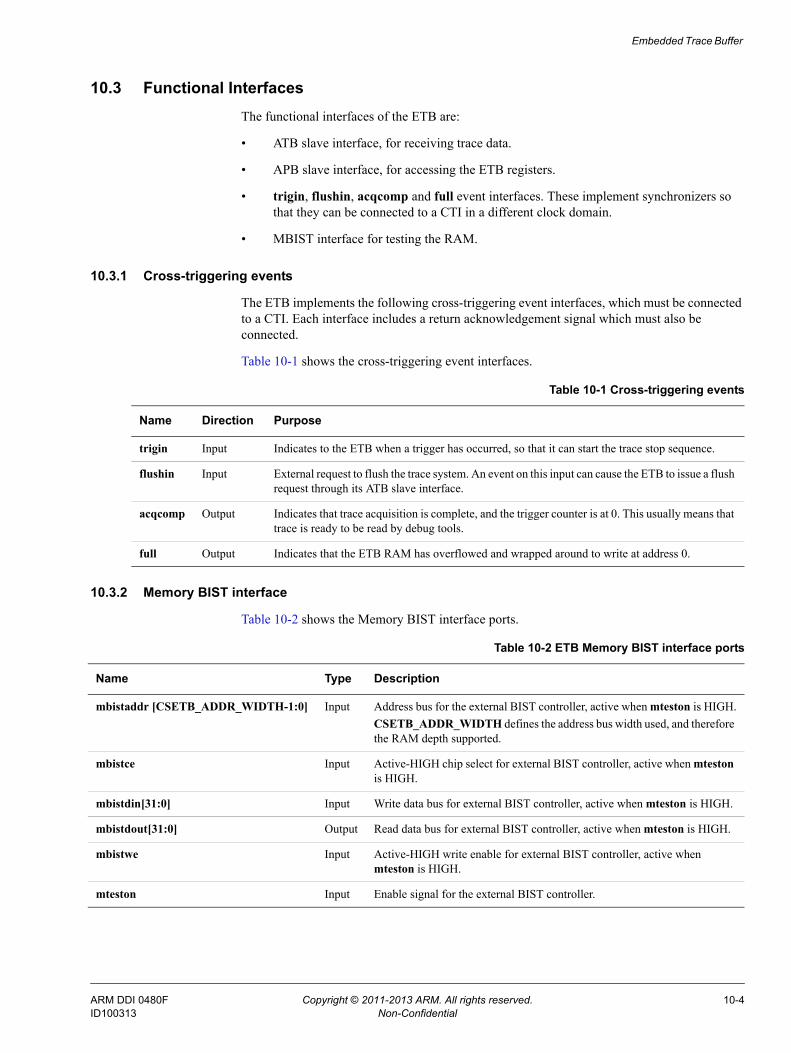
Embedded Trace Buffer
10.3 Functional InterfacesThe functional interfaces of the ETB are:
• ATB slave interface, for receiving trace data.
• APB slave interface, for accessing the ETB registers.
• trigin, flushin, acqcomp and full event interfaces. These implement synchronizers so that they can be connected to a CTI in a different clock domain.
• MBIST interface for testing the RAM.
10.3.1 Cross-triggering events
The ETB implements the following cross-triggering event interfaces, which must be connected to a CTI. Each interface includes a return acknowledgement signal which must also be connected.
Table 10-1 shows the cross-triggering event interfaces.
10.3.2 Memory BIST interface
Table 10-2 shows the Memory BIST interface ports.
Table 10-1 Cross-triggering events
Name Direction Purpose
trigin Input Indicates to the ETB when a trigger has occurred, so that it can start the trace stop sequence.
flushin Input External request to flush the trace system. An event on this input can cause the ETB to issue a flush request through its ATB slave interface.
acqcomp Output Indicates that trace acquisition is complete, and the trigger counter is at 0. This usually means that trace is ready to be read by debug tools.
full Output Indicates that the ETB RAM has overflowed and wrapped around to write at address 0.
Table 10-2 ETB Memory BIST interface ports
Name Type Description
mbistaddr [CSETB_ADDR_WIDTH-1:0] Input Address bus for the external BIST controller, active when mteston is HIGH.CSETB_ADDR_WIDTH defines the address bus width used, and therefore the RAM depth supported.
mbistce Input Active-HIGH chip select for external BIST controller, active when mteston is HIGH.
mbistdin[31:0] Input Write data bus for external BIST controller, active when mteston is HIGH.
mbistdout[31:0] Output Read data bus for external BIST controller, active when mteston is HIGH.
mbistwe Input Active-HIGH write enable for external BIST controller, active when mteston is HIGH.
mteston Input Enable signal for the external BIST controller.
ARM DDI 0480F Copyright © 2011-2013 ARM. All rights reserved. 10-4ID100313 Non-Confidential

Embedded Trace Buffer
10.4 ETB trace capture and formattingThe formatter inserts the source ID signal atids[6:0] into a special format data packet stream to enable trace data to be reassociated with a trace source after data is read back out of the ETB. The formatter protocol is described in the ARM® CoreSight™ Architecture Specification.
10.4.1 Modes of operation
The formatter supports the following distinct modes of operation as specified by bits[1:0] in the FFCR, described in ETB Formatter and Flush Control Register on page 3-77:
Bypass In this mode, no formatting information is inserted into the trace stream and a raw reproduction of the incoming trace stream is stored.When trace is stopped, an additional byte of value 0x01 is written, followed by bytes of 0x00 to align the trace to a 32-bit boundary. This can be used by a trace decompressor to find the last byte of trace.
Note • This mode assumes that the source ID does not change.
• To select this mode, set FFCR.EnFTC to 0 and FFCR.EnFCont to 0.
Normal Formatting information is added to indicate the change of source ID together with the associated wrapping additions, as described in ARM® CoreSight™ Architecture Specification. When tracing is stopped, the formatter frame is filled with bytes of trace with ID 0x00 if necessary to complete the frame.To select this mode, set FFCR.EnFTC to 1 and FFCR.EnFCont to 0.
Continuous Continuous mode in the ETB corresponds to normal mode with the embedding of triggers. Most usage models use this mode, and modern debug tools do not normally require the other modes. Unlike continuous mode in the TPIU, no formatter synchronization packets are added because the formatted trace frames are always aligned to the RAM address.To select this mode, set FFCR.EnFTC to 1 and FFCR.EnFCont to 1.
10.4.2 Stopping trace
Trace capture stops when any of the following occur:
• The TraceCaptEn bit of the Control Register is cleared.
• A trigger event occurs and the Trigger Counter Register reaches zero.
• A flush completes and the StopFl bit of the Formatter and Flush Control Register is set.
When trace capture stops, the FtStopped bit of the Formatter and Flush Status Register is set.
Figure 10-1 on page 10-6 shows the conditions for stopping trace capture. This figure refers to bits from the ETB Control register on page 3-75 and the ETB Formatter and Flush Control Register on page 3-77.
ARM DDI 0480F Copyright © 2011-2013 ARM. All rights reserved. 10-5ID100313 Non-Confidential

Embedded Trace Buffer
Figure 10-1 Conditions for stopping trace capture
StopTrig and StopFl in the FFCR can be enabled at the same time. For example, if FOnTrig in the FFCR is set to perform a flush on a trigger event, but StopTrig is HIGH, none of the flushed data is stored, because StopTrig is HIGH. If the situation requires that all the flushed data is captured, then StopTrig is LOW and StopFl is HIGH.
After trace capture stops, the ETB discards any additional trace it receives on the ATB slave interface prevent an ATB bus from stalling. This is important when a replicator is present, but the received data is ignored.
10.4.3 Flush assertion
All three flush-generating conditions can be enabled together:• Flush from flushin.• Flush from trigger.• Manually activated flush.
Is TraceCaptEn
0?
CtlReg = Trace Capture Enable (master ETB enable register)
Is StopFl HIGH?
Is StopTrig HIGH?
Has a flush just finished?
Is trigin rising from 0 to 1?
Yes
No
Yes
NoNo
Yes
Yes
No
Yes
Start
Currently inserting a trigger packet?
No
Yes
Is Trigger Counter now at
0 and was at 0?
Is Trigger Counter now at
0 and was at 1?
No
No No
If EnFCont set, and TrigEvt or TrigIn set, has
trigger been inserted?
Output StopReq HIGH to formatter
Yes
Yes
Yes
ARM DDI 0480F Copyright © 2011-2013 ARM. All rights reserved. 10-6ID100313 Non-Confidential

Embedded Trace Buffer
If more flush events are generated while a flush is in progress, the current flush is serviced before the next flush is started. Only one request for each source of flush can be pended. If a subsequent flush request signal is deasserted while the flush is still being serviced or pended, a second flush is not generated.
Figure 10-2 shows generation of flush on flushin.
Figure 10-2 Generation of flush on flushin
Figure 10-3 on page 10-8 shows generation of flush from a trigger event.
Start
Is the formatter stopped?
Is ‘FOnFlIn’
set?
Is flushin rising from 0 to 1?
Alternate flush already in
progress?
Pend flush request
Active flush complete?
Flush on flushin in progress
Request flush on ATB slave interface
No
Yes
Yes
No
No
Yes
Yes
No
Clear pending
flush
Yes
No
FFSR[1] = 1
FFCR[4] = 1
flushin port rising
Manual flush or Flush on trigger already in progress
Manual flush or Flush on trigger completed?
Generate a Flush on flushin request
ARM DDI 0480F Copyright © 2011-2013 ARM. All rights reserved. 10-7ID100313 Non-Confidential
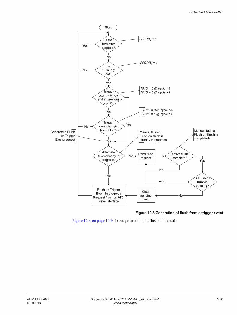
Embedded Trace Buffer
Figure 10-3 Generation of flush from a trigger event
Figure 10-4 on page 10-9 shows generation of a flush on manual.
Start
Is the formatter stopped?
Is ‘FOnTrig’
set?
Trigger count = 0 now and in previous
cycle?
Alternate flush already in
progress?
Pend flush request
Active flush complete?
Flush on Trigger Event in progress
Request flush on ATB slave interface
No
Yes
Yes
No
Yes
No
Clear pending
flush
No
FFSR[1] = 1
FFCR[5] = 1
TRIG = 0 @ cycle t & TRIG = 0 @ cycle t-1
Manual flush or Flush on flushin already in progress
Manual flush or Flush on flushin completed?
Trigger count changing
from 1 to 0?
Yes
Generate a Flush on Trigger
Event request
TRIG = 0 @ cycle t & TRIG = 1 @ cycle t-1
No
Yes
Is Flush on flushin
pending?
Yes
No
Yes
No
ARM DDI 0480F Copyright © 2011-2013 ARM. All rights reserved. 10-8ID100313 Non-Confidential

Embedded Trace Buffer
Figure 10-4 Generation of a flush on manual
10.4.4 Triggers
A trigger event is defined as when:• The trigger counter reaches 0.• The trigger counter is 0 and trigin is HIGH.
All trigger indication conditions, TrigEvt, TrigFl, and TrigIn, in the FFCR can be enabled simultaneously. This results in multiple triggers appearing in the trace stream.
The trigger counter register controls how many words are written into the trace RAM after a trigger event. After the formatter is flushed in normal or continuous mode, a complete empty frame is generated. This is a data overhead of seven extra words in the worst case. The trigger counter defines the number of 32-bit words remaining to be stored in the ETB trace RAM. If the formatter is in bypass mode, a maximum of two additional words are stored for the trace capture post-amble. See Modes of operation on page 10-5.
Figure 10-5 on page 10-10 shows a flowchart defining the conditions for indicating a trigger in the formatted data. This flowchart only applies for the condition when continuous formatting is enabled (EnFCont set) in the Formatter and Flush Control Register.
Start
Is ‘FOnFlIn’ set?No
FFCR[6] = 1
Generate a manual flush request
Alternate flush already in
progress?
Pend flush request
Active flush complete?Yes
No
No
Flush on flushin or Flush on trigger already in progress
Flush on flushin or Flush on trigger completed?Yes
Is Flush on flushin or Flush on trigger pending?
Yes
Yes
No
Manual Flush in progress
Request flush on ATB slave interface
Clear pending
flush
ARM DDI 0480F Copyright © 2011-2013 ARM. All rights reserved. 10-9ID100313 Non-Confidential

Embedded Trace Buffer
Figure 10-5 Generation of a trigger request with continuos formatting enabled
Is trigin rising from 0 to 1?
Is Trigger Counter now at 0
and previously at 0?
*Is Trigger Counter now at 0 and previously at
1?
*Is trigin rising from 0 to 1?
Insert a trigger packet into the
formatted trace.
Yes
No No
No
No
Has an ATB flush just completed?
No
No
No
Yes
Yes
Yes
Yes
Yes
No
Is TrigIn set?
Is TrigEvt set?
Start
Is TrigFl set?
Is StopReq HIGH?
Yes
Yes
Yes
* Denotes a trigger event
When StopReq goes HIGH at the same time as a trigger packet is inserted, the trigger packet is inserted first.
ARM DDI 0480F Copyright © 2011-2013 ARM. All rights reserved. 10-10ID100313 Non-Confidential
Embedded Trace Buffer
10.5 ETB RAM supportThe following sections describe the ETB RAM support:• Access sizes.• BIST interface.• RAM instantiation.
10.5.1 Access sizes
All reads and writes to the RAM are 32 bits. The ETB does not require byte write support.
10.5.2 BIST interface
The RAM BIST interface connects though the trace RAM interface block to provide test access to the trace RAM. mteston enables the memory BIST interface and disables all other accesses to and from the RAM.
10.5.3 RAM instantiation
For information about integrating the ETB RAM, see the ARM® CoreSight™ SoC-400 Implementation Guide.
ARM DDI 0480F Copyright © 2011-2013 ARM. All rights reserved. 10-11ID100313 Non-Confidential

Appendix A Signal Descriptions
This appendix describes the CoreSight SoC-400 port and interface signals. It contains the following sections:• Debug Access Port signals on page A-2.• APB component signals on page A-14.• ATB interconnect signals on page A-18.• Timestamp component signals on page A-25.• Trigger component signals on page A-32.• Trace sink signals on page A-35.• Authentication and event bridges on page A-38.• Granular power requestor signals on page A-40.
ARM DDI 0480F Copyright © 2011-2013 ARM. All rights reserved. A-1ID100313 Non-Confidential

Signal Descriptions
A.1 Debug Access Port signalsThe section describes the DAP signals. It contains the following subsections:• Serial wire or JTAG Debug Port signals on page A-3.• DAPBUS interconnect signals on page A-5.• DAPBUS asynchronous bridge signals on page A-5.• DAPBUS synchronous bridge signals on page A-7.• JTAG - Access Port signals on page A-9.• AXI - Access Port signals on page A-9.• AHB - Access Port signals on page A-11.• APB - Access Port signals on page A-13.
ARM DDI 0480F Copyright © 2011-2013 ARM. All rights reserved. A-2ID100313 Non-Confidential

Signal Descriptions
A.1.1 Serial wire or JTAG Debug Port signals
Table A-1 shows the Serial Wire or JTAG Debug Port (SWJ-DP) signals.
Table A-1 Serial wire and JTAG debug port signals
Name Type Clock domain Description
ntrst Input swclktck TAP asynchronous reset.
npotrst Input swclktck JTAG powerup reset and Serial wire powerup reset.
swclktck Input NA Serial wire clock and TAP clock.
swditms Input swclktck Serial wire data input and TAP test mode select.
tdi Input swclktck JTAG TAP data in or alternative input function.
dapresetn Input dapclk DAP asynchronous reset active-LOW.
dapclk Input dapclk DAP clock.
dapclken Input dapclk DAP clock enable.
daprdata[31:0] Input dapclk DAP read data.
dapready Input dapclk DAP data bus ready.
dapslverr Input dapclk AP slave error response.
cdbgpwrupack Input None Debug power domain up acknowledge.
csyspwrupack Input None System power domain up acknowledge.
cdbgrstack Input None Debug reset acknowledge to reset controller.
targetid[31:0] Input None Target ID for SW multi-drop selection.
instanceid[3:0] Input None Instance ID for SW multi-drop selection.
swdo Output swclktck Serial wire data output.
swdoen Output swclktck Serial wire data output enable.
tdo Output swclktck JTAG TAP data out.
ntdoen Output swclktck TAP data out enable.
dapcaddr[15:2] Output dapclk Compressed DAP address.
dapwrite Output dapclk DAP bus write.
dapenable Output dapclk DAP enable transaction.
dapabort Output dapclk DAP abort.
dapsel Output dapclk DAP transaction select.
dapwdata[31:0] Output dapclk DAP write data.
cdbgpwrupreq Output NA Debug power domain powerup request.
csyspwrupreq Output NA System power domain powerup request.
ARM DDI 0480F Copyright © 2011-2013 ARM. All rights reserved. A-3ID100313 Non-Confidential

Signal Descriptions
cdbgrstreq Output NA Debug reset request to reset controller.
jtagnsw Output swclktck HIGH If JTAG selected.LOW If SWD selected.
jtagtop Output swclktck JTAG state machine is in one of the four modes:• Test-Logic-Reset.• Run-Test/Idle.• Select-DR-Scan.• Select-IR-Scan.
Table A-1 Serial wire and JTAG debug port signals (continued)
Name Type Clock domain Description
ARM DDI 0480F Copyright © 2011-2013 ARM. All rights reserved. A-4ID100313 Non-Confidential

Signal Descriptions
A.1.2 DAPBUS interconnect signals
Table A-2 shows the DAPBUS interconnect signals.
A.1.3 DAPBUS asynchronous bridge signals
Table A-3 shows the DAPBUS asynchronous bridge signals.
Table A-2 DAPBUS interconnect signals
Name Type Clock domain Description
clk Input clk DAP Clock.
resetn Input clk DAP Reset.
daprdatam31<x>[31:0] Input clk DAP read data bus.
dapreadym<x> Input clk DAP ready.
dapslverrm<x> Input clk DAP error.
dapcaddrs[15:2] Input clk DAP compressed address bus.
dapsels Input clk DAP select.
dapenables Input clk DAP enable.
dapwrites Input clk DAP write or read.
dapwdatas[31:0] Input clk DAP write data bus.
dapaborts Input clk DAP abort.
dapcaddrm<x>[7:2] Output clk DAP compressed address bus.
dapselm<x> Output clk DAP select.
dapenablem<x> Output clk DAP enable.
dapwritem<x> Output clk DAP write or read.
dapwdatam<x>[31:0] Output clk DAP write data bus.
dapabortm<x> Output clk DAP abort.
daprdatas[31:0] Output clk DAP read data bus.
dapreadys Output clk DAP ready.
dapslverrs Output clk DAP error.
Table A-3 DAPBUS asynchronous bridge signals
Signal Type Clock domain Description
dapclks Input dapclks DAP clock.
dapclkens Input dapclks DAP clock enable.
dapresetsn Input dapclks DAP reset.
dapclkenm Input dapclks DAP clock enable.
dapclkm Input dapclkm DAP clock.
ARM DDI 0480F Copyright © 2011-2013 ARM. All rights reserved. A-5ID100313 Non-Confidential

Signal Descriptions
Cross-domain connections
The DAPBUS asynchronous bridge can be configured as a separate master interface component and slave interface component. If you configure the bridge in this way, then you must connect the two components as Table A-4 on page A-7 shows.
dapresetm Input dapclks DAP reset.
dapsels Input dapclks The DAP select signal. Indicates that the DAP bus master is selecting this slave device and requires a data transfer.
dapaborts Input dapclks The DAP abort. When the bus master asserts dapaborts HIGH, the DAP slave aborts the present DAP transfer and asserts dapreadys HIGH in the next cycle.
dapenables Input dapclks The DAP enable. Indicates the second and subsequent cycles of a DAP transfer.
dapwrites Input dapclks The DAP RW select signal. It indicates a DAP write access when HIGH and a DAP read access when LOW.
dapaddrs[31:0] Input dapclks The DAP address bus.
dapwdatas[31:0] Input dapclks The DAP write data bus.
dapreadym Input dapclkm The DAP ready. The slave indicates whether it has completed present transfer and is ready for the next transfer.
dapslverrm Input dapclkm The DAP slave error. The slave indicates that the present transfer has a error.
daprdatam[31:0] Input dapclkm The DAP read data. The read data of the present DAP read transfer.
csysreqa Input dapclks Clock powerdown request.
dapreadys Output dapclks The DAP ready. The DAP bus slave asserts this signal HIGH to indicate that it completed the current DAP transfer and is ready for the next transfer.
dapslverrs Output dapclks The DAP slave error. When HIGH, the DAP slave indicates that the present DAP transaction had an error.
daprdatas[31:0] Output dapclks The DAP read data. Carries the read data of a DAP read transfer.
dapselm Output dapclkm The DAP select. Indicates that the master is selecting a particular slave for RW transfer.
dapabortm Output dapclkm The DAP abort. When asserted HIGH, it indicates that the master is aborting the present transaction.
dapenablem Output dapclkm The DAP enable. Indicates the second and subsequent cycles of a DAP transfer.
dapwritem Output dapclkm The DAP RW. Indicates a write transfer when HIGH and a read transfer when LOW.
dapaddrm[31:0] Output dapclkm The DAP address bus.
dapwdatam[31:0] Output dapclkm The DAP write data. The master drives this bus and carries the write data for the present write transfer.
csysacka Output dapclks Clock powerdown acknowledge.
cactivea Output dapclks Clock is required when driven HIGH.
a. This signal is only present if you configure this component to have an LPI.
Table A-3 DAPBUS asynchronous bridge signals (continued)
Signal Type Clock domain Description
ARM DDI 0480F Copyright © 2011-2013 ARM. All rights reserved. A-6ID100313 Non-Confidential

Signal Descriptions
Table A-4 shows DAPBUS asynchronous bridge cross-domain connections
A.1.4 DAPBUS synchronous bridge signals
Table A-5 shows the DAPBUS synchronous bridge signals.
Table A-4 DAPBUS asynchronous bridge cross-domain connections
Slave component signal Type Master component signal Type
dapm_req_async Output daps_req_async Input
dapm_ack_async Input daps_ack_async Output
dapm_fwd_data_async Output daps_fwd_data_async Input
dapm_rev_data_async Input daps_rev_data_async Output
dapm_abort_req_async Output daps_abort_req_async Input
Table A-5 DAPBUS synchronous bridge signals
Signal Type Clock domain Description
dapclk Input dapclk The DAP clock.
dapresetn Input dapclk The DAP reset.
dapclkens Input dapclk The DAP clock enable.
dapsels Input dapclk The DAP select. Indicates that the slave device is selected and a data transfer is required.
dapaborts Input dapclk The DAP abort. When this signal is asserted HIGH, then the DAP slave aborts the current DAP transfer and asserts dapreadys HIGH in the next cycle.
dapenables Input dapclk The DAP enable. Indicates the second and subsequent cycles of a DAP transfer
dapwrites Input dapclk The DAP RW. Indicates a DAP write access when HIGH and a DAP read access when LOW.
dapaddrs[31:0] Input dapclk The DAP address bus from master.
dapwdatas[31:0] Input dapclk The DAP write data. The DAP master drives this bus.
dapclkenm Input dapclk The DAP clock enable.
dapreadym Input dapclk The DAP ready. The slave indicates whether it has completed the current transfer and is ready for the next transfer.
dapslverrm Input dapclk The DAP slave error. The slave indicates that the present transfer has an error.
daprdatam[31:0] Input dapclk The DAP read data. The read data of the present DAP read transfer.
csysreq Input dapclk Clock powerdown request.
dapreadys Output dapclk The DAP slave ready. When asserted HIGH, it indicates that the slave completed the present DAP transfer and is ready for the next transfer.
dapslverrs Output dapclk The DAP slave error. Indicates that the present DAP transaction has an error.
daprdatas[31:0] Output dapclk The DAP read data. Carries the read data of a DAP read transfer.
dapselm Output dapclk The DAP select. Indicates that the master is selecting a particular slave for RW transfer.
ARM DDI 0480F Copyright © 2011-2013 ARM. All rights reserved. A-7ID100313 Non-Confidential

Signal Descriptions
dapabortm Output dapclk The DAP master abort. When asserted HIGH, it indicates that the master is aborting the current transaction.
dapenablem Output dapclk The DAP enable. Indicates the second and subsequent cycles of a DAP transfer.
dapwritem Output dapclk The DAP RW. Indicates a write transfer when HIGH and a read transfer when LOW.
dapaddrm[31:0] Output dapclk The DAP address bus.
dapwdatam[31:0] Output dapclk The DAP write data. The master drives this bus and carries the write data for the current write transfer.
csysack Output dapclk Clock powerdown acknowledge.
cactive Output dapclk Clock is required when driven HIGH.
Table A-5 DAPBUS synchronous bridge signals (continued)
Signal Type Clock domain Description
ARM DDI 0480F Copyright © 2011-2013 ARM. All rights reserved. A-8ID100313 Non-Confidential
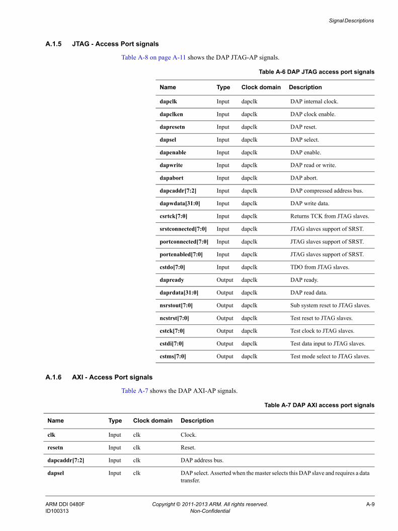
Signal Descriptions
A.1.5 JTAG - Access Port signals
Table A-8 on page A-11 shows the DAP JTAG-AP signals.
A.1.6 AXI - Access Port signals
Table A-7 shows the DAP AXI-AP signals.
Table A-6 DAP JTAG access port signals
Name Type Clock domain Description
dapclk Input dapclk DAP internal clock.
dapclken Input dapclk DAP clock enable.
dapresetn Input dapclk DAP reset.
dapsel Input dapclk DAP select.
dapenable Input dapclk DAP enable.
dapwrite Input dapclk DAP read or write.
dapabort Input dapclk DAP abort.
dapcaddr[7:2] Input dapclk DAP compressed address bus.
dapwdata[31:0] Input dapclk DAP write data.
csrtck[7:0] Input dapclk Returns TCK from JTAG slaves.
srstconnected[7:0] Input dapclk JTAG slaves support of SRST.
portconnected[7:0] Input dapclk JTAG slaves support of SRST.
portenabled[7:0] Input dapclk JTAG slaves support of SRST.
cstdo[7:0] Input dapclk TDO from JTAG slaves.
dapready Output dapclk DAP ready.
daprdata[31:0] Output dapclk DAP read data.
nsrstout[7:0] Output dapclk Sub system reset to JTAG slaves.
ncstrst[7:0] Output dapclk Test reset to JTAG slaves.
cstck[7:0] Output dapclk Test clock to JTAG slaves.
cstdi[7:0] Output dapclk Test data input to JTAG slaves.
cstms[7:0] Output dapclk Test mode select to JTAG slaves.
Table A-7 DAP AXI access port signals
Name Type Clock domain Description
clk Input clk Clock.
resetn Input clk Reset.
dapcaddr[7:2] Input clk DAP address bus.
dapsel Input clk DAP select. Asserted when the master selects this DAP slave and requires a data transfer.
ARM DDI 0480F Copyright © 2011-2013 ARM. All rights reserved. A-9ID100313 Non-Confidential

Signal Descriptions
dapenable Input clk The DAP enable. Indicates the second and subsequent cycles of a DAP transfer.
dapwrite Input clk The DAP RW. Indicates a DAP write access when HIGH and a DAP read access when LOW.
dapwdata[31:0] Input clk The DAP write data.
dapabort Input clk The DAP abort. When this signal is asserted HIGH, then the DAP slave aborts the present DAP transfer and asserts in the next cycle.
dbgen Input clk Debug enable for AHB transfers.
spiden Input clk Secure Privileged Invasive Debug Enable. Prevents secure transfer initiation when LOW.
awready Input clk Write address ready.
wready Input clk Write data ready.
bresp[1:0] Input clk Write response.
bvalid Input clk Write response valid.
arready Input clk Read address ready.
rdata[63:0] Input clk Read data.
rresp[1:0] Input clk Read data response.
rlast Input clk Read data last transfer indication.
rvalid Input clk Read data valid.
rombaseaddrl[31:0] Input clk Least significant 32-bit of the AXI-AP Debug Base Address Register.
rombaseaddru[31:0] Input clk Most significant 32-bit of the AXI-AP Debug Base Address Register.
daprdata[31:0] Output clk The DAP read data. Carries the read data of a DAP read transfer.
dapready Output clk The DAP ready. When asserted HIGH, it indicates that the slave completed the present DAP transfer and is ready for the next transfer.
dapslverr Output clk The DAP slave error. Indicates that the present DAP transaction has an error.
awaddr[63:0] Output clk Write address.
awlen[3:0] Output clk Write burst length.
awsize[2:0] Output clk Write burst size.
awburst[1:0] Output clk Write burst type.
awlock Output clk Write lock type.
awcache[3:0] Output clk Write cache type.
awprot[2:0] Output clk Write protection type.
awvalid Output clk Write address valid.
wdata[63:0] Output clk Write data.
wstrb[7:0] Output clk Write byte-lane strobes.
Table A-7 DAP AXI access port signals (continued)
Name Type Clock domain Description
ARM DDI 0480F Copyright © 2011-2013 ARM. All rights reserved. A-10ID100313 Non-Confidential

Signal Descriptions
A.1.7 AHB - Access Port signals
Table A-8 shows the DAP AHB-AP signals.
wlast Output clk Write data last transfer indication.
wvalid Output clk Write data valid.
bready Output clk Write response ready.
araddr[63:0] Output clk Read address.
arlen[3:0] Output clk Read burst length.
arsize[2:0] Output clk Read burst size.
arburst[1:0] Output clk Read burst type.
arlock Output clk Read lock type.
arcache[3:0] Output clk Read cache type.
arprot[2:0] Output clk Read protection type.
arvalid Output clk Read address valid.
rready Output clk Read data ready.
awdomain[1:0] Output clk Write domain.
awsnoop[2:0] Output clk Write snoop request type.
awbar[1:0] Output clk Write barrier type.
ardomain[1:0] Output clk Write domain.
arsnoop[3:0] Output clk Read snoop request type.
arbar[1:0] Output clk Read barriers.
Table A-7 DAP AXI access port signals (continued)
Name Type Clock domain Description
Table A-8 DAP AHB access port signals
Signal Type Clock domain Description
dapabort Input dapclk DAP abort.
dapcaddr[7:2] Input dapclk DAP compressed address bus.
dapclk Input dapclk DAP clock.
dapclken Input dapclk DAP clock enable.
dapenable Input dapclk DAP enable.
dapresetn Input dapclk DAP reset.
dapsel Input dapclk DAP select.
dapwdata[31:0] Input dapclk DAP write data bus.
dapwrite Input dapclk DAP write or read.
dbgen Input dapclk Debug enable for AHB transfers.
ARM DDI 0480F Copyright © 2011-2013 ARM. All rights reserved. A-11ID100313 Non-Confidential

Signal Descriptions
hrdatam Input dapclk AHB read data bus.
hreadym Input dapclk AHB slave ready.
hrespm Input dapclk AHB slave response.
spiden Input dapclk Secure Privileged Invasive Debug Enable. Prevents secure transfer initiation when LOW.
rombaseaddr[31:0] Input dapclk Static port to define the AHB ROM table base address.
daprdata[31:0] Output dapclk DAP read data bus.
dapready Output dapclk DAP ready.
dapslverr Output dapclk DAP slave error.
haddrm[31:0] Output dapclk AHB address bus.
hbstrbm[3:0] Output dapclk AHB byte lane strobe.
hburstm[2:0] Output dapclk AHB burst type.
hlockm Output dapclk AHB lock transfer.
hprotm[6:0] Output dapclk AHB protection type.
hsizem[2:0] Output dapclk AHB transfer size.
htransm[1:0] Output dapclk AHB transfer type.
hwdatam[31:0] Output dapclk AHB write data bus.
hwritem Output dapclk AHB write or read.
Table A-8 DAP AHB access port signals (continued)
Signal Type Clock domain Description
ARM DDI 0480F Copyright © 2011-2013 ARM. All rights reserved. A-12ID100313 Non-Confidential
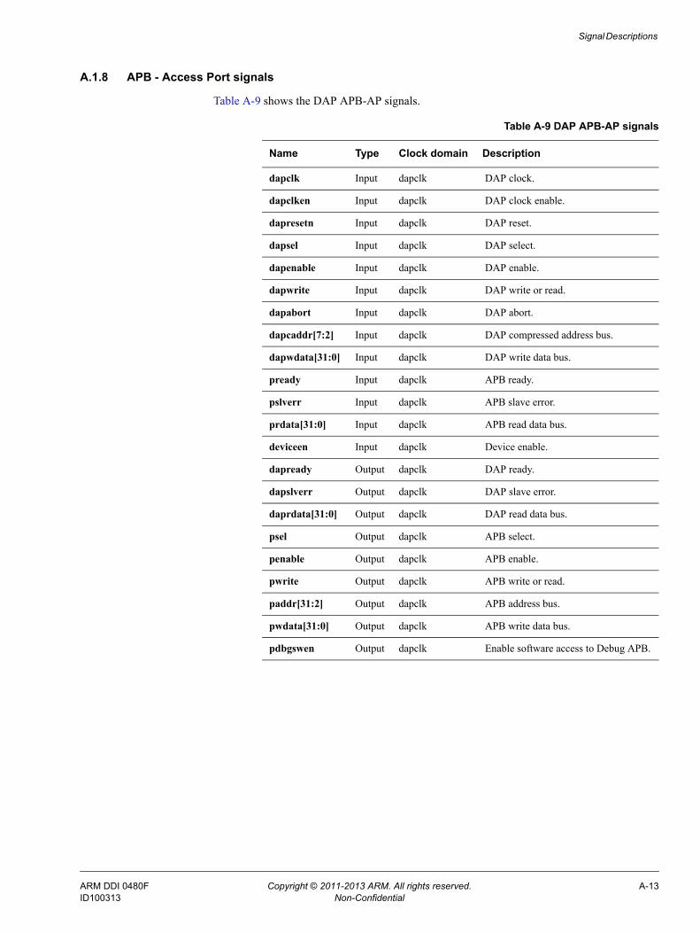
Signal Descriptions
A.1.8 APB - Access Port signals
Table A-9 shows the DAP APB-AP signals.
Table A-9 DAP APB-AP signals
Name Type Clock domain Description
dapclk Input dapclk DAP clock.
dapclken Input dapclk DAP clock enable.
dapresetn Input dapclk DAP reset.
dapsel Input dapclk DAP select.
dapenable Input dapclk DAP enable.
dapwrite Input dapclk DAP write or read.
dapabort Input dapclk DAP abort.
dapcaddr[7:2] Input dapclk DAP compressed address bus.
dapwdata[31:0] Input dapclk DAP write data bus.
pready Input dapclk APB ready.
pslverr Input dapclk APB slave error.
prdata[31:0] Input dapclk APB read data bus.
deviceen Input dapclk Device enable.
dapready Output dapclk DAP ready.
dapslverr Output dapclk DAP slave error.
daprdata[31:0] Output dapclk DAP read data bus.
psel Output dapclk APB select.
penable Output dapclk APB enable.
pwrite Output dapclk APB write or read.
paddr[31:2] Output dapclk APB address bus.
pwdata[31:0] Output dapclk APB write data bus.
pdbgswen Output dapclk Enable software access to Debug APB.
ARM DDI 0480F Copyright © 2011-2013 ARM. All rights reserved. A-13ID100313 Non-Confidential

Signal Descriptions
A.2 APB component signalsThe section describes the APB component signals. It contains the following subsections:• APB interconnect signals.• APB asynchronous bridge signals on page A-15.• APB synchronous bridge signals on page A-16.
A.2.1 APB interconnect signals
Table A-10 shows the APB interconnect signals.
Table A-10 APB interconnect signals
Signal Type Clock domain Description
clk Input clk The clock reference signal for all APB debug interfaces. The rising edge of clk times all transfers on the APB.
resetn Input clk Active-LOW reset.
prdatam<x>[31:0]c Input clk APB read data. Drives this bus during read cycles.
preadym<x>c Input clk APB ready. Uses this signal to extend an APB transfer.
pslverrm<x>c Input clk Indicates a transfer failure. The APB peripherals are not required to support the pslverr pin.
paddrs<x>[saw:2]ab Input clk The APB address bus for slave interface <x>.
psels<x>a Input clk Select. Indicates that the slave interface <x> is selected, and a data transfer is required.
penables<x>a Input clk Enable. Indicates the second and subsequent cycles of an APB transfer initiated on slave interface <x>.
pwrites<x>a Input clk Direction. Indicates an APB write access when HIGH and an APB read access when LOW.
pwdatas<x>[31:0]a Input clk Write data that the APB master device connected to the APBIC slave interface <x> drives.
targetid[31:0] Input clk Provides information to uniquely identify the sub system connected to this APBIC.
paddr31s0 Input clk Enables components to distinguish between internal accesses from system software, and external accesses from a debugger.
dbgswen Input clk Enable software access to debug APB.
paddrm<x>[maw:2]cd Output clk The APB address bus for master interface <x>.
pselm<x>c Output clk APB select. Indicates that the slave device connected to master interface <x> is selected, and a data transfer is required.
penablem<x>c Output clk APB enable. Indicates the second and subsequent cycles of an APB transfer that the master interface <x> initiates.
pwritem<x>c Output clk APB RW transfer. Indicates an APB write access when HIGH, and an APB read access when LOW.
pwdatam<x>[31:0]c Output clk Write data that the APBIC master interface <x> drives.
ARM DDI 0480F Copyright © 2011-2013 ARM. All rights reserved. A-14ID100313 Non-Confidential

Signal Descriptions
A.2.2 APB asynchronous bridge signals
Table A-11 shows the APB asynchronous bridge signals.
prdatas<x>[31:0]a Output clk Read data. The slave interface <x> drives this bus during read cycles.
preadys<x>a Output clk APB ready. The slave interface <x> uses this signal to extend an APB transfer.
pslverrs<x>a Output clk Indicates a transfer failure.
a. Where <x>=0 to (NUM_SLAVE_INTF-1).b. Where saw is a parameter dependent number.c. Where <x>=0 to (NUM_MASTER_INTF-1).d. Where maw is a parameter dependent number.
Table A-10 APB interconnect signals (continued)
Signal Type Clock domain Description
Table A-11 APB asynchronous bridge signals
Signal Type Clock domain Description
pclks Input pclks APB clock.
presetsn Input pclks APB reset.
pclkens Input pclks APB clock enable.
pclkm Input pclkm APB clock.
presetmn Input pclkm APB reset.
pclkenm Input pclkm APB clock enable.
psels Input pclks APB select. Indicates that the slave interface is selected and a data transfer is required.
penables Input pclks APB enable. Indicates the second and subsequent cycles of an APB transfer initiated on slave interface.
pwrites Input pclks APB RW transfer. Indicates an APB write access when HIGH and an APB read access when LOW.
paddrs[31:0] Input pclks APB address bus.
pwdatas[31:0] Input pclks APB write data.
preadym Input pclkm APB ready. The slave device uses this signal to extend an APB transfer.
pslverrm Input pclkm APB transfer error. Indicates a transfer failure. The APB peripherals are not required to support the pslverr pin.
prdatam[31:0] Input pclkm APB read data. The selected slave drives this bus during read cycles.
csysreqa Input pclkm Clock powerdown request.
preadys Output pclks APB ready. The slave interface uses this signal to extend an APB transfer.
pslverrs Output pclks APB transfer error. Indicates a transfer failure. The APB peripherals are not required to support the pslverr pin.
prdatas[31:0] Output pclks APB read data. The slave interface drives this bus during read cycles.
ARM DDI 0480F Copyright © 2011-2013 ARM. All rights reserved. A-15ID100313 Non-Confidential

Signal Descriptions
Cross-domain connections
The APB asynchronous bridge can be configured as a separate master interface component and slave interface component. If you configure the bridge in this way, then you must connect the two components as Table A-12 shows.
Table A-12 shows APB asynchronous bridge cross-domain connections.
A.2.3 APB synchronous bridge signals
Table A-13 shows the APB synchronous bridge signals.
pselm Output pclkm APB select. Indicates that the slave device connected to the master interface is selected and a data transfer is required.
penablem Output pclkm APB enable. Indicates the second and subsequent cycles of an APB transfer that the master interface initiates.
pwritem Output pclkm APB RW transfer. Indicates an APB write access when HIGH and an APB read access when LOW.
paddrm[31:0] Output pclkm APB address bus.
pwdatam[31:0] Output pclkm APB write data. The APB master interface drives this bus.
csysacka Output pclkm Clock powerdown acknowledge.
cactivea Output pclkm Clock is required when driven HIGH.
a. This signal is present only if you configure this component to have a low-power interface, and it configured for master-only or full.
Table A-11 APB asynchronous bridge signals (continued)
Signal Type Clock domain Description
Table A-12 APB asynchronous bridge cross-domain connections
Slave component signal Type Master component signal Type
apbm_req_async Output apbs_req_async Input
apbm_ack_async Input apbs_ack_async Output
apbm_fwd_data_async Output apbs_fwd_data_async Input
apbm_rev_data_async Input apbs_rev_data_async Output
Table A-13 APB synchronous bridge signals
Signal Type Clock domain Description
pclk Input pclk APB clock signal for all downstream APB debug interfaces.
presetn Input pclk APB reset.
pclkens Input pclk APB clock enable.
psels Input pclk APB select. Indicates that the slave interface is selected and a data transfer is required.
penables Input pclk APB enable. Indicates the second and subsequent cycles of an APB transfer initiated on slave interface.
ARM DDI 0480F Copyright © 2011-2013 ARM. All rights reserved. A-16ID100313 Non-Confidential
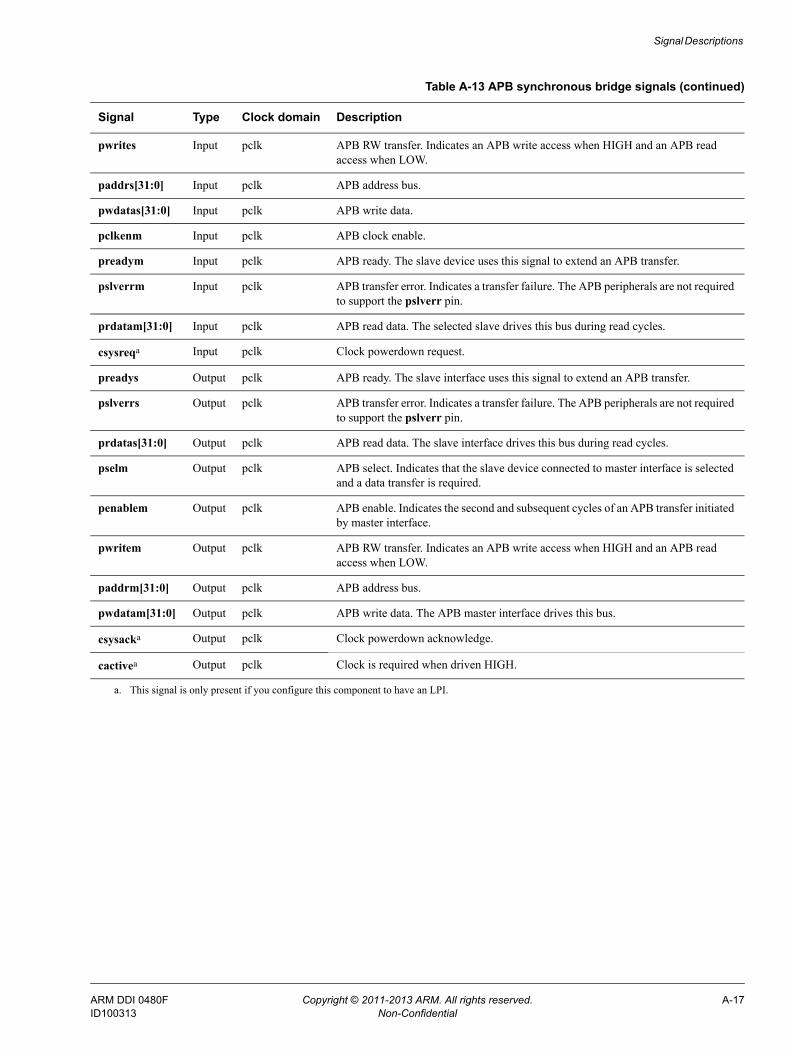
Signal Descriptions
pwrites Input pclk APB RW transfer. Indicates an APB write access when HIGH and an APB read access when LOW.
paddrs[31:0] Input pclk APB address bus.
pwdatas[31:0] Input pclk APB write data.
pclkenm Input pclk APB clock enable.
preadym Input pclk APB ready. The slave device uses this signal to extend an APB transfer.
pslverrm Input pclk APB transfer error. Indicates a transfer failure. The APB peripherals are not required to support the pslverr pin.
prdatam[31:0] Input pclk APB read data. The selected slave drives this bus during read cycles.
csysreqa Input pclk Clock powerdown request.
preadys Output pclk APB ready. The slave interface uses this signal to extend an APB transfer.
pslverrs Output pclk APB transfer error. Indicates a transfer failure. The APB peripherals are not required to support the pslverr pin.
prdatas[31:0] Output pclk APB read data. The slave interface drives this bus during read cycles.
pselm Output pclk APB select. Indicates that the slave device connected to master interface is selected and a data transfer is required.
penablem Output pclk APB enable. Indicates the second and subsequent cycles of an APB transfer initiated by master interface.
pwritem Output pclk APB RW transfer. Indicates an APB write access when HIGH and an APB read access when LOW.
paddrm[31:0] Output pclk APB address bus.
pwdatam[31:0] Output pclk APB write data. The APB master interface drives this bus.
csysacka Output pclk Clock powerdown acknowledge.
cactivea Output pclk Clock is required when driven HIGH.
a. This signal is only present if you configure this component to have an LPI.
Table A-13 APB synchronous bridge signals (continued)
Signal Type Clock domain Description
ARM DDI 0480F Copyright © 2011-2013 ARM. All rights reserved. A-17ID100313 Non-Confidential

Signal Descriptions
A.3 ATB interconnect signalsThis section describes the following component signals:• ATB replicator signals.• ATB trace funnel signals on page A-19.• ATB upsizer signals on page A-20.• ATB downsizer signals on page A-21.• ATB asynchronous bridge signals on page A-22.• ATB synchronous bridge signals on page A-23.
A.3.1 ATB replicator signals
Table A-14 shows the ATB replicator signals.
Table A-14 ATB replicator signals
Name Type Clock domain Description
afreadys Input clk ATB data flush complete on the slave port.
afvalidm0 Input clk ATB data flush request on the master port 0.
afvalidm1 Input clk ATB data flush request on the master port 1.
atbytess[<bw>:0] a Input clk ATB number of valid bytes, LSB aligned, on the slave port.
clk Input clk ATB clock.
atdatas[<dw>:0] b Input clk ATB trace data.
atids[6:0] Input clk ATB ID for current trace data.
atreadym0 Input clk ATB transfer ready on master port 0.
atreadym1 Input clk ATB transfer ready on master port 1.
resetn Input clk ATB reset.
atvalids Input clk ATB valid signal present.
paddrdbg[11:2] Input clk Debug APB address bus.
penabledbg Input clk Debug APB enable signal, indicates second and subsequent cycles.
pseldbg Input clk Debug APB component select.
pwdatadbg[31:0] Input clk Debug APB write data bus.
pwritedbg Input clk Debug APB write transfer.
pclkendbg Input clk Debug APB clock enable.
paddrdbg31 Input clk Enables components to distinguish between internal accesses from system software, and external accesses from a debugger.
syncreqm0 Input clk Synchronization request.
syncreqm1 Input clk Synchronization request.
afreadym0 Output clk ATB data flush complete for the master port 0.
afreadym1 Output clk ATB data flush complete for the master port 1.
afvalids Output clk ATB data flush request for the master port.
ARM DDI 0480F Copyright © 2011-2013 ARM. All rights reserved. A-18ID100313 Non-Confidential

Signal Descriptions
A.3.2 ATB trace funnel signals
Table A-15 shows the ATB trace funnel signals.
atbytesm0[<bw>:0] b Output clk ATB number of valid bytes, LSB aligned, on the master port.
atbytesm1[<bw>:0] b Output clk ATB number of valid bytes, LSB aligned, on the master port.
atdatam0[<dw>:0]c Output clk ATB trace data on the master port 0.
atdatam1[<dw>:0]c Output clk ATB trace data on the master port 1.
atidm0[6:0] Output clk ATB ID for current trace data on master port 0.
atidm1[6:0] Output clk ATB ID for current trace data on master port 1.
atreadys Output clk ATB transfer ready.
atvalidm0 Output clk ATB valid signal present on master port 0.
atvalidm1 Output clk ATB valid signal present on master port 1.
preadydbg Output clk Debug APB ready signal.
prdatadbg[31:0] Output clk Debug APB read data bus.
pslverrdbg Output clk Debug APB transfer error signal.
syncreqs Output clk Synchronization request.
a. <bw> has a value in the range 0-3 that is calculated at configuration time.b. <dw> is the width of the data bus minus one.
Table A-14 ATB replicator signals (continued)
Name Type Clock domain Description
Table A-15 ATB trace funnel signals
Name Type Clock domain Description
afreadys<x>a Input clk ATB data flush complete for the slave port <x>.
afvalidm Input clk ATB data flush request for the master port.
atbytess<x>[<bw>:0]ab Input clk ATB number of valid bytes, LSB aligned, on the slave port <x>.
clk Input clk ATB clock.
atdatas<x>[<dw>:0] ac Input clk ATB trace data on the slave port <x>.
atids<x>[6:0] a Input clk ATB ID for current trace data on slave port <x>.
atreadym Input clk ATB transfer ready on master port.
resetn Input clk ATB reset.
atvalids<x>a Input clk ATB valid signal present on slave port <x>.
paddrdbg[11:2] Input clk Debug APB address bus.
paddrdbg31 Input clk Enables components to distinguish between internal accesses from system software, and external accesses from a debugger.
pclkendbg Input clk Debug APB clock enable.
ARM DDI 0480F Copyright © 2011-2013 ARM. All rights reserved. A-19ID100313 Non-Confidential
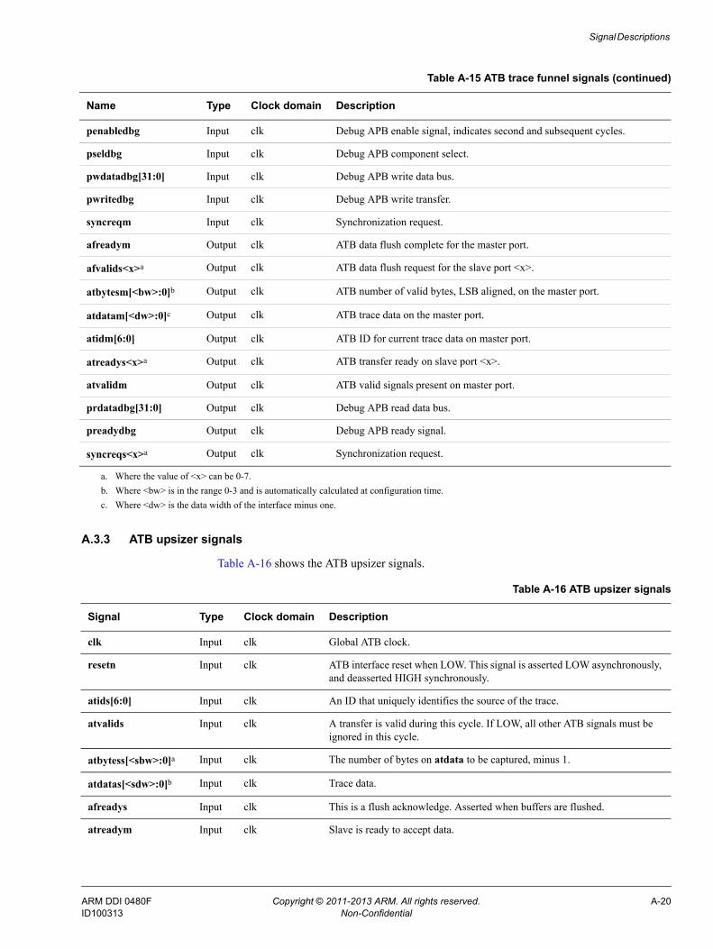
Signal Descriptions
A.3.3 ATB upsizer signals
Table A-16 shows the ATB upsizer signals.
penabledbg Input clk Debug APB enable signal, indicates second and subsequent cycles.
pseldbg Input clk Debug APB component select.
pwdatadbg[31:0] Input clk Debug APB write data bus.
pwritedbg Input clk Debug APB write transfer.
syncreqm Input clk Synchronization request.
afreadym Output clk ATB data flush complete for the master port.
afvalids<x>a Output clk ATB data flush request for the slave port <x>.
atbytesm[<bw>:0]b Output clk ATB number of valid bytes, LSB aligned, on the master port.
atdatam[<dw>:0]c Output clk ATB trace data on the master port.
atidm[6:0] Output clk ATB ID for current trace data on master port.
atreadys<x>a Output clk ATB transfer ready on slave port <x>.
atvalidm Output clk ATB valid signals present on master port.
prdatadbg[31:0] Output clk Debug APB read data bus.
preadydbg Output clk Debug APB ready signal.
syncreqs<x>a Output clk Synchronization request.
a. Where the value of <x> can be 0-7.b. Where <bw> is in the range 0-3 and is automatically calculated at configuration time.c. Where <dw> is the data width of the interface minus one.
Table A-15 ATB trace funnel signals (continued)
Name Type Clock domain Description
Table A-16 ATB upsizer signals
Signal Type Clock domain Description
clk Input clk Global ATB clock.
resetn Input clk ATB interface reset when LOW. This signal is asserted LOW asynchronously, and deasserted HIGH synchronously.
atids[6:0] Input clk An ID that uniquely identifies the source of the trace.
atvalids Input clk A transfer is valid during this cycle. If LOW, all other ATB signals must be ignored in this cycle.
atbytess[<sbw>:0]a Input clk The number of bytes on atdata to be captured, minus 1.
atdatas[<sdw>:0]b Input clk Trace data.
afreadys Input clk This is a flush acknowledge. Asserted when buffers are flushed.
atreadym Input clk Slave is ready to accept data.
ARM DDI 0480F Copyright © 2011-2013 ARM. All rights reserved. A-20ID100313 Non-Confidential
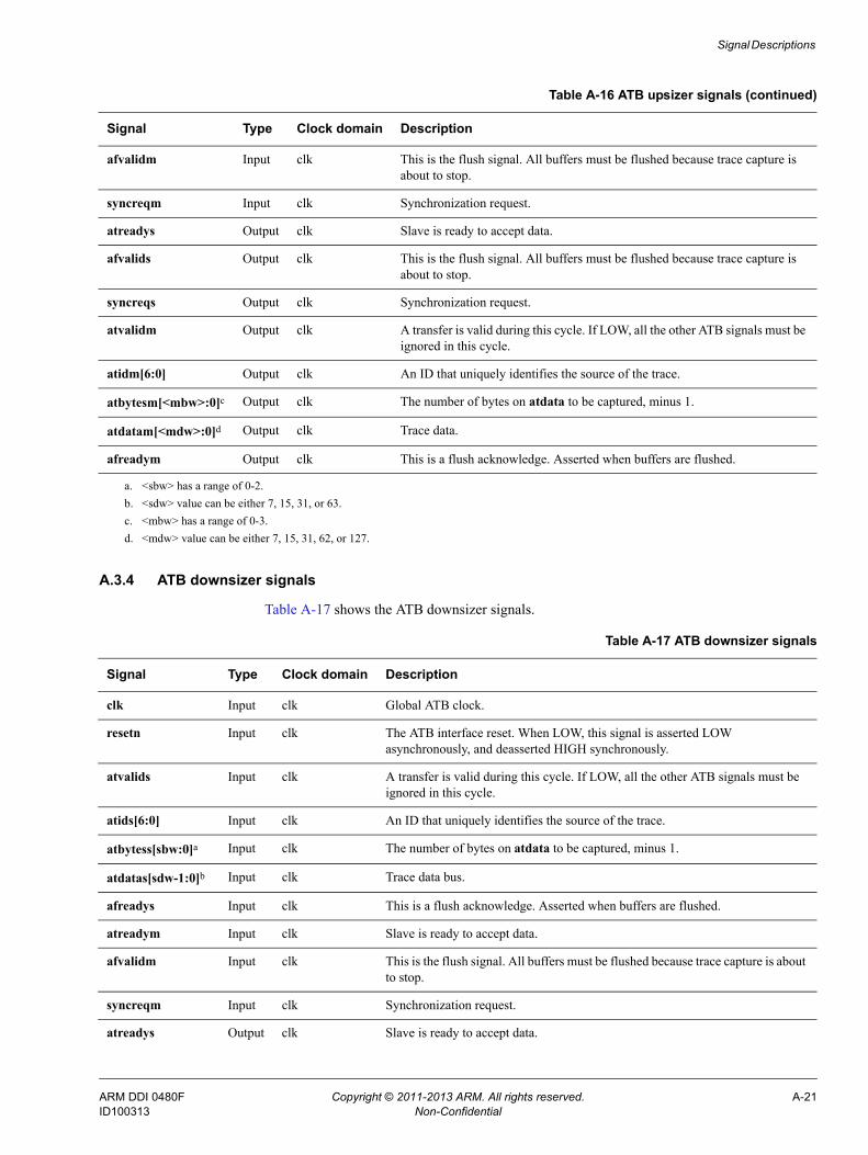
Signal Descriptions
A.3.4 ATB downsizer signals
Table A-17 shows the ATB downsizer signals.
afvalidm Input clk This is the flush signal. All buffers must be flushed because trace capture is about to stop.
syncreqm Input clk Synchronization request.
atreadys Output clk Slave is ready to accept data.
afvalids Output clk This is the flush signal. All buffers must be flushed because trace capture is about to stop.
syncreqs Output clk Synchronization request.
atvalidm Output clk A transfer is valid during this cycle. If LOW, all the other ATB signals must be ignored in this cycle.
atidm[6:0] Output clk An ID that uniquely identifies the source of the trace.
atbytesm[<mbw>:0]c Output clk The number of bytes on atdata to be captured, minus 1.
atdatam[<mdw>:0]d Output clk Trace data.
afreadym Output clk This is a flush acknowledge. Asserted when buffers are flushed.
a. <sbw> has a range of 0-2.b. <sdw> value can be either 7, 15, 31, or 63.c. <mbw> has a range of 0-3.d. <mdw> value can be either 7, 15, 31, 62, or 127.
Table A-16 ATB upsizer signals (continued)
Signal Type Clock domain Description
Table A-17 ATB downsizer signals
Signal Type Clock domain Description
clk Input clk Global ATB clock.
resetn Input clk The ATB interface reset. When LOW, this signal is asserted LOW asynchronously, and deasserted HIGH synchronously.
atvalids Input clk A transfer is valid during this cycle. If LOW, all the other ATB signals must be ignored in this cycle.
atids[6:0] Input clk An ID that uniquely identifies the source of the trace.
atbytess[sbw:0]a Input clk The number of bytes on atdata to be captured, minus 1.
atdatas[sdw-1:0]b Input clk Trace data bus.
afreadys Input clk This is a flush acknowledge. Asserted when buffers are flushed.
atreadym Input clk Slave is ready to accept data.
afvalidm Input clk This is the flush signal. All buffers must be flushed because trace capture is about to stop.
syncreqm Input clk Synchronization request.
atreadys Output clk Slave is ready to accept data.
ARM DDI 0480F Copyright © 2011-2013 ARM. All rights reserved. A-21ID100313 Non-Confidential

Signal Descriptions
A.3.5 ATB asynchronous bridge signals
Table A-18 shows the ATB asynchronous bridge signals.
afvalids Output clk This is the flush signal. All buffers must be flushed because trace capture is about to stop.
syncreqs Output clk Synchronization request.
atvalidm Output clk A transfer is valid during this cycle. If LOW, all other ATB signals must be ignored in this cycle.
atidm[6:0] Output clk An ID that uniquely identifies the source of the trace.
atbytesm[mbw:0]c Output clk The number of bytes on ATDATA to be captured, minus 1.
atdatam[mdw:0]d Output clk Trace data bus.
afreadym Output clk This is a flush acknowledge. Asserted when buffers are flushed.
a. Where sbw can have the range 0-3 and is automatically calculated at configuration time based on the data width of the slave interface.b. Where sdw is the data width of the slave interface.c. Where mbw can have the range 0-3 and is automatically calculated at configuration time based on the data width of the master interface.d. Where mdw is the data width of the master interface.
Table A-17 ATB downsizer signals (continued)
Signal Type Clock domain Description
Table A-18 ATB asynchronous bridge signals
Name Type Clock domain Description
clks Input clks ATB clock.
resetsn Input clks ATB reset.
clkens Input clks ATB clock enable.
clkm Input clkm ATB clock.
resetmn Input clkm ATB reset.
clkenm Input clkm ATB clock enable.
atvalids Input clks ATB valid signal.
atreadym Input clkm ATB transfer ready.
atids[6:0] Input clks ATB ID for the present trace data.
atbytess[bw:0]a Input clks ATB number of valid bytes, LSB aligned, on the slave port.
atdatas[dw:0]b Input clks ATB trace data.
afvalidm Input clkm ATB data flush request.
afreadys Input clks ATB data flush complete.
afreadym Input clkm ATB data flush complete.
syncreqm Input clks Synchronization request.
csysreqc Input clks Clock powerdown request.
ARM DDI 0480F Copyright © 2011-2013 ARM. All rights reserved. A-22ID100313 Non-Confidential
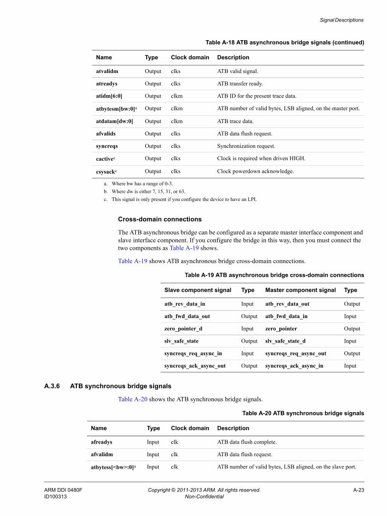
Signal Descriptions
Cross-domain connections
The ATB asynchronous bridge can be configured as a separate master interface component and slave interface component. If you configure the bridge in this way, then you must connect the two components as Table A-19 shows.
Table A-19 shows ATB asynchronous bridge cross-domain connections.
A.3.6 ATB synchronous bridge signals
Table A-20 shows the ATB synchronous bridge signals.
atvalidm Output clks ATB valid signal.
atreadys Output clks ATB transfer ready.
atidm[6:0] Output clkm ATB ID for the present trace data.
atbytesm[bw:0]a Output clkm ATB number of valid bytes, LSB aligned, on the master port.
atdatam[dw:0] Output clkm ATB trace data.
afvalids Output clks ATB data flush request.
syncreqs Output clks Synchronization request.
cactivec Output clks Clock is required when driven HIGH.
csysackc Output clks Clock powerdown acknowledge.
a. Where bw has a range of 0-3.b. Where dw is either 7, 15, 31, or 63.c. This signal is only present if you configure the device to have an LPI.
Table A-18 ATB asynchronous bridge signals (continued)
Name Type Clock domain Description
Table A-19 ATB asynchronous bridge cross-domain connections
Slave component signal Type Master component signal Type
atb_rev_data_in Input atb_rev_data_out Output
atb_fwd_data_out Output atb_fwd_data_in Input
zero_pointer_d Input zero_pointer Output
slv_safe_state Output slv_safe_state_d Input
syncreqs_req_async_in Input syncreqs_req_async_out Output
syncreqs_ack_async_out Output syncreqs_ack_async_in Input
Table A-20 ATB synchronous bridge signals
Name Type Clock domain Description
afreadys Input clk ATB data flush complete.
afvalidm Input clk ATB data flush request.
atbytess[<bw>:0]a Input clk ATB number of valid bytes, LSB aligned, on the slave port.
ARM DDI 0480F Copyright © 2011-2013 ARM. All rights reserved. A-23ID100313 Non-Confidential

Signal Descriptions
clk Input clk ATB clock.
clkens Input clk ATB clock enable.
clkenm Input clk ATB clock enable.
atdatas[<dw>:0]b Input clk ATB trace data.
atids[6:0] Input clk ATB ID for the present trace data.
atreadym Input clk ATB transfer ready.
resetn Input clk ATB reset for the ATCLK domain.
atvalids Input clk ATB valid signal present.
csysreqc Input clk Clock powerdown request.
syncreqm Input clk Synchronization request.
afreadym Output clk ATB data flush complete.
afvalids Output clk ATB data flush request.
atbytesm[<bw>:0]b Output clk ATB number of valid bytes, LSB aligned, on the master port.
atdatam[<dw>:0]b Output clk ATB trace data.
atidm Output clk ATB ID for current trace data.
atreadys Output clk ATB transfer ready.
atvalidm Output clk ATB valid signals present.
cactivec Output clk Clock is required when driven HIGH.
csysackc Output clk Clock powerdown acknowledge.
syncreqs Output clk Synchronization request.
a. <bw> has a range of 0-3.b. <dw> is the data width of the interface, minus one.c. This signal is only present if you configure the device to have an LPI.
Table A-20 ATB synchronous bridge signals (continued)
Name Type Clock domain Description
ARM DDI 0480F Copyright © 2011-2013 ARM. All rights reserved. A-24ID100313 Non-Confidential

Signal Descriptions
A.4 Timestamp component signalsThis section describes timestamp component signals in the following sections:• Timestamp generator signals.• Timestamp encoder signals on page A-26.• Narrow timestamp replicator signals on page A-27.• Narrow timestamp asynchronous bridge signals on page A-27.• Narrow timestamp synchronous bridge signals on page A-29.• Timestamp decoder signals on page A-30.• Timestamp interpolator signals on page A-31.
A.4.1 Timestamp generator signals
Table A-21 shows the timestamp generator signals.
Table A-21 Timestamp generator signals
Name Type Clock domain Description
clk Input clk APB clock.
resetn Input clk APB reset.
hltdbg Input clk Request to halt the counter when the processor is in debug state.
paddrctrl[11:2] Input clk APB address.
pselctrl Input clk APB select. Indicates that the slave interface is selected and a data transfer is required.
penablectrl Input clk APB enable. Indicates the second and subsequent cycles of a transfer initiated on a slave interface.
pwritectrl Input clk APB RW transfer. Indicates an APB write access when HIGH and an APB read access when LOW.
pwdatactrl[31:0] Input clk APB write data. This bus is driven by the APB master device connected to slave interface.
paddrread[11:2] Input clk APB address.
pselread Input clk APB select. Indicates that the slave interface is selected and a data transfer is required.
penableread Input clk APB enable. Indicates the second and subsequent cycles of a transfer initiated on a slave interface.
pwriteread Input clk APB RW transfer. Indicates an APB write access when HIGH and an APB read access when LOW. Because this is an RO interface, writes have no effect.
pwdataread[31:0] Input clk APB write data. The APB master device connected to slave interface drives this bus. Because this is an RO interface, writes have no effect.
tsvalueb[63:0] Output clk Wide timestamp value in binary.
tsforcesync Output clk Resynchronization request.
preadyctrl Output clk APB ready. The slave device uses this signal to extend an APB transfer.
pslverrctrl Output clk Indicates a transfer failure.
prdatactrl[31:0] Output clk APB read data. The slave interface drives this bus during read cycles.
ARM DDI 0480F Copyright © 2011-2013 ARM. All rights reserved. A-25ID100313 Non-Confidential

Signal Descriptions
A.4.2 Timestamp encoder signals
Table A-22 shows the timestamp encoder signals.
preadyread Output clk APB ready. The slave device uses this signal to extend an APB transfer.
pslverrread Output clk Indicates a transfer failure.
prdataread[31:0] Output clk APB read data. Slave interface drives this bus during read cycles.
Table A-21 Timestamp generator signals (continued)
Name Type Clock domain Description
Table A-22 Timestamp encoder signals
Name Type Clock domain Description
tsclk Input tsclk Timestamp clock.
tsresetn Input tsclk Timestamp reset.
tsvalue[63:0] Input tsclk Timestamp generator interface value.
tsforcesync Input tsclk Timestamp generator interface force synchronization.
tssyncready Input tsclk Timestamp slave ready.
tsbit[6:0] Output tsclk Timestamp encoded value.
tssync[1:0] Output tsclk Timestamp synchronization bits.
ARM DDI 0480F Copyright © 2011-2013 ARM. All rights reserved. A-26ID100313 Non-Confidential

Signal Descriptions
A.4.3 Narrow timestamp replicator signals
Table A-23 shows the narrow timestamp replicator signals.
A.4.4 Narrow timestamp asynchronous bridge signals
Table A-24 shows the narrow timestamp asynchronous bridge signals.
Table A-23 Narrow timestamp replicator signals
Name Type Clock domain Description
clk Input clk Timestamp clock.
resetn Input clk Timestamp reset.
tssyncreadym<x> Input clk Timestamp slave ready.
tsbits[6:0] Input clk Timestamp encoded value.
tssyncs[1:0] Input clk Timestamp synchronization bits.
tsbitm<x>[6:0]a
a. Where <x> can have any value in the range 0-15.
Output clk Timestamp encoded value.
tssyncm<x>[1:0] Output clk Timestamp synchronization bits.
tssyncreadys Output clk Timestamp slave ready.
Table A-24 Narrow timestamp asynchronous bridge signals
Name Type Clock domain Description
clkm Input clkm Clock.
resetmn Input clkm Reset.
clks Input clks Clock.
resetsn Input clks Reset.
tsbits[6:0] Input clks Timestamp encoded value.
tssyncs[1:0] Input clks Timestamp synchronization bits.
csysreqa
a. This signal is only present if you configure the device to have an LPI.
Input clks Clock powerdown request.
tssyncreadym Input clkm Timestamp slave ready.
tssyncreadys Output clks Timestamp slave ready.
csysacka Output clks Clock powerdown acknowledge.
cactivea Output clks Clock is required when driven HIGH.
tsbitm[6:0] Output clkm Timestamp encoded value.
tssyncm[1:0] Output clkm Timestamp synchronization bits.
ARM DDI 0480F Copyright © 2011-2013 ARM. All rights reserved. A-27ID100313 Non-Confidential

Signal Descriptions
Cross-domain connections
The narrow timestamp asynchronous bridge can be configured as a separate master interface component and slave interface component. If you configure the bridge in this way, then you must connect the two components as Table A-25 shows.
Table A-25 shows narrow timestamp asynchronous bridge cross-domain connections.
Table A-25 Narrow timestamp asynchronous bridge cross-domain connections
Slave component signal Type Master component signal Type
wr_ptr_gry_s Output wr_ptr_gry_m Input
encd_data_s Output end_data_m Input
rd_ptr_gry_s Input rd_ptr_gry_m Output
rd_ptr_bin_s Input rd_ptr_bin_m Output
lp_req_s Output lp_req_m Input
lp_ack_s Input lp_ack_m Output
ARM DDI 0480F Copyright © 2011-2013 ARM. All rights reserved. A-28ID100313 Non-Confidential

Signal Descriptions
A.4.5 Narrow timestamp synchronous bridge signals
Table A-26 shows the narrow timestamp synchronous bridge signals.
Table A-26 Narrow timestamp synchronous bridge signals
Name Type Clock domain Description
clk Input clk Clock.
resetn Input clk Reset.
clkens Input clk Clock enable.
clkenm Input clk Clock enable.
tsbits[6:0] Input clk Timestamp encoded value.
tssyncs[1:0] Input clk Timestamp synchronization bits.
tssyncreadym Input clk Timestamp slave ready.
csysreqa
a. This signal is only present if you configure the device to have an LPI.
Input clk Clock powerdown request.
tssyncreadys Output clk Timestamp slave ready.
tsbitm[6:0] Output clk Timestamp encoded value.
tssyncm[1:0] Output clk Timestamp synchronization bits.
csysacka Output clk Clock powerdown acknowledge.
cactivea Output clk Clock is required when driven HIGH.
ARM DDI 0480F Copyright © 2011-2013 ARM. All rights reserved. A-29ID100313 Non-Confidential

Signal Descriptions
A.4.6 Timestamp decoder signals
Table A-27 shows the timestamp decoder signals.
Table A-27 Timestamp decoder signals
Name Type Clock domain Description
clk Input clk Clock.
resetn Input clk Reset.
tsbit[6:0] Input clk Timestamp encoded value.
tssync[1:0] Input clk Timestamp synchronization bits.
tssyncready Output clk Timestamp slave ready.
tsvalue[63:0] Output clk Timestamp decoded value. The original value exported from the timestamp generator.
ARM DDI 0480F Copyright © 2011-2013 ARM. All rights reserved. A-30ID100313 Non-Confidential

Signal Descriptions
A.4.7 Timestamp interpolator signals
Table A-28 shows the timestamp interpolator signals.
Table A-28 Timestamp interpolator signals
Name Type Clock domain Description
clk Input clk Clock.
resetn Input clk Reset.
tsvalueb[63:0] Input clk Timestamp value.
tsvalueintpb[63:0] Output clk Interpolated timestamp value.
ARM DDI 0480F Copyright © 2011-2013 ARM. All rights reserved. A-31ID100313 Non-Confidential

Signal Descriptions
A.5 Trigger component signalsThis section describes the ECT signals in the following sections:• Cross Trigger Interface signals.• Cross Trigger Matrix signals on page A-33.• Event asynchronous bridge signals on page A-34.
A.5.1 Cross Trigger Interface signals
Table A-29 shows the CTI signals.
Table A-29 CTI signals
Name Type Clock domain Description
cihsbypass[3:0] Input cticlk Channel interface handshake bypass.
cisbypass Input cticlk Channel interface sync bypass.
ctiapbsbypass Input cticlk Synchronization bypass between APB and CTI clock.
ctichin[3:0] Input cticlk Channel in.
ctichoutack[3:0] Input cticlk Channel out acknowledge.
cticlk Input cticlk CTI clock.
cticlken Input cticlk CTI clock enable.
ctitrigin[7:0] Input cticlk Trigger in.
ctitrigoutack[7:0] Input cticlk Trigger out acknowledge.
dbgen Input NA Invasive debug enable.
ctiresetn Input cticlk Reset.
niden Input cticlk Non-invasive debug enable.
paddrdbg[11:2] Input pclkdbg Debug APB address bus.
paddrdbg31 Input pclkdbg Enables components to distinguish between internal accesses from system software and external accesses from a debugger.
pclkdbg Input pclkdbg Debug APB clock.
pclkendbg Input pclkdbg Debug APB clock enable.
penabledbg Input pclkdbg Debug APB enable signal, indicates second and subsequent cycles.
presetdbgn Input pclkdbg Debug APB reset.
pseldbg Input pclkdbg Debug APB component select.
pwdatadbg[31:0] Input pclkdbg Debug APB write data bus.
pwritedbg Input pclkdbg Debug APB write transfer.
se Input N/A Scan enable.
tihsbypass[7:0] Input cticlk Trigger interface handshake bypass, static value.
tinidensel[7:0] Input cticlk Masks when NIDEN is LOW, static value.
tisbypassack[7:0] Input cticlk Trigger out acknowledge sync bypass, static value.
ARM DDI 0480F Copyright © 2011-2013 ARM. All rights reserved. A-32ID100313 Non-Confidential

Signal Descriptions
A.5.2 Cross Trigger Matrix signals
Table A-30 shows the CTM signals.
tisbypassin[7:0] Input cticlk Trigger in sync bypass, static value.
todbgensel[7:0] Input cticlk Masks when dbgen is LOW, static value.
asicctl[7:0] Output cticlk External multiplexer control.
ctichinack[3:0] Output cticlk Channel in acknowledge.
ctichout[3:0] Output cticlk Channel out.
ctitriginack[7:0] Output cticlk Trigger in acknowledge.
ctitrigout[7:0] Output cticlk Trigger out.
prdatadbg[31:0] Output pclkdbg Debug APB read data bus.
preadydbg Output pclkdbg Debug APB ready signal.
Table A-29 CTI signals (continued)
Name Type Clock domain Description
Table A-30 CTM signals
Name Type Clock domain Description
cihsbypass0[3:0] Input ctmclk Handshaking bypass port 0.
cihsbypass1[3:0] Input ctmclk Handshaking bypass port 1.
cihsbypass2[3:0] Input ctmclk Handshaking bypass port 2.
cihsbypass3[3:0] Input ctmclk Handshaking bypass port 3.
cisbypass0 Input ctmclk Sync bypass for port 0.
cisbypass1 Input ctmclk Sync bypass for port 1.
cisbypass2 Input ctmclk Sync bypass for port 2.
cisbypass3 Input ctmclk Sync bypass for port 3.
ctmchin0[3:0] Input ctmclk Channel in port 0.
ctmchin1[3:0] Input ctmclk Channel in port 1.
ctmchin2[3:0] Input ctmclk Channel in port 2.
ctmchin3[3:0] Input ctmclk Channel in port 3.
ctmchoutack0[3:0] Input ctmclk Channel out acknowledge port 0.
ctmchoutack1[3:0] Input ctmclk Channel out Acknowledge port 1.
ctmchoutack2[3:0] Input ctmclk Channel out acknowledge port 2.
ctmchoutack3[3:0] Input ctmclk Channel out acknowledge port 3.
ctmclk Input ctmclk Clock.
ctmclken Input ctmclk Clock enable.
ctmresetn Input ctmclk Reset.
ARM DDI 0480F Copyright © 2011-2013 ARM. All rights reserved. A-33ID100313 Non-Confidential
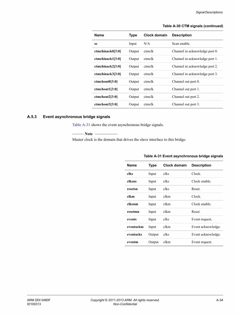
Signal Descriptions
A.5.3 Event asynchronous bridge signals
Table A-31 shows the event asynchronous bridge signals.
Note Master clock is the domain that drives the slave interface to this bridge.
se Input N/A Scan enable.
ctmchinack0[3:0] Output ctmclk Channel in acknowledge port 0.
ctmchinack1[3:0] Output ctmclk Channel in acknowledge port 1.
ctmchinack2[3:0] Output ctmclk Channel in acknowledge port 2.
ctmchinack3[3:0] Output ctmclk Channel in acknowledge port 3.
ctmchout0[3:0] Output ctmclk Channel out port 0.
ctmchout1[3:0] Output ctmclk Channel out port 1.
ctmchout2[3:0] Output ctmclk Channel out port 2.
ctmchout3[3:0] Output ctmclk Channel out port 3.
Table A-30 CTM signals (continued)
Name Type Clock domain Description
Table A-31 Event asynchronous bridge signals
Name Type Clock domain Description
clks Input clks Clock.
clkens Input clks Clock enable.
resetsn Input clks Reset.
clkm Input clkm Clock.
clkenm Input clkm Clock enable.
resetmn Input clkm Reset.
events Input clks Event request.
eventackm Input clkm Event acknowledge.
eventacks Output clks Event acknowledge.
eventm Output clkm Event request.
ARM DDI 0480F Copyright © 2011-2013 ARM. All rights reserved. A-34ID100313 Non-Confidential

Signal Descriptions
A.6 Trace sink signalsThis section describes the following component signals:• Trace Port Interface Unit signals.• Embedded Trace Buffer signals on page A-36.
A.6.1 Trace Port Interface Unit signals
Table A-32 shows the TPIU signals.
Table A-32 TPIU signals
name Type clock domain Description
afreadys Input atclk ATB data flush complete for the master port.
atbytess[1:0] Input atclk ATB number of valid bytes, LSB aligned, on the slave port.
atclk Input atclk ATB clock.
atclken Input atclk ATB clock enable.
atdatas[31:0] Input atclk ATB trace data on the slave port.
atids[6:0] Input atclk ATB ID for current trace data on slave port.
atresetn Input atclk ATB reset for the atclk domain.
atvalids Input atclk ATB valid signals present on slave port.
extctlin[7:0] Input atclk External control input.
flushin Input atclk Flush input from the CTI.
paddrdbg[11:2] Input pclkdbg Debug APB address bus.
paddrdbg31 Input pclkdbg Enables components to distinguish between internal accesses from system software and external accesses from a debugger.
pclkdbg Input pclkdbg Debug APB clock.
pclkendbg Input pclkdbg Debug APB clock enable.
penabledbg Input pclkdbg Debug APB enable signal, indicates second and subsequent cycles.
presetdbgn Input pclkdbg Debug APB asynchronous reset.
pseldbg Input pclkdbg Debug APB component select.
pwdatadbg[31:0] Input pclkdbg Debug APB write data bus.
pwritedbg Input pclkdbg Debug APB write transfer.
se Input N/A Scan enable.
tpctl Input atclk Tie-off to report presence of tracectl, static value.
tpmaxdatasize[4:0] Input atclk Tie-off to report maximum number of pins on tracedata, static value.
traceclkin Input traceclkin Trace clock.
tresetn Input traceclkin Trace clock asynchronous reset.
trigin Input atclk Trigger input from the CTI.
afvalids Output atclk ATB data flush request for the master port.
ARM DDI 0480F Copyright © 2011-2013 ARM. All rights reserved. A-35ID100313 Non-Confidential

Signal Descriptions
A.6.2 Embedded Trace Buffer signals
Table A-33 shows the ETB signals.
atreadys Output atclk ATB transfer ready on slave port.
extctlout[7:0] Output atclk External control output.
flushinack Output atclk Flush input acknowledgement.
prdatadbg[31:0] Output pclkdbg Debug APB read data bus.
preadydbg Output pclkdbg Debug APB ready signal.
traceclk Output traceclkin Half the frequency of the exported trace port clock, traceclkin.
tracectl Output traceclkin Trace port control.
tracedata[31:0] Output traceclkin Trace port data.
triginack Output atclk Trigger input acknowledgement.
Table A-32 TPIU signals (continued)
name Type clock domain Description
Table A-33 ETB signals
Name Type Clock domain Description
afreadys Input atclk ATB data flush complete.
atbytess[1:0] Input atclk ATB number of valid bytes, LSB aligned, on the slave port.
atclk Input atclk ATB clock.
atclken Input atclk ATB clock enable.
atdatas[31:0] Input atclk ATB trace data.
atids[6:0] Input atclk ATB ID for the current trace data.
atresetn Input atclk ATB reset for the atclk domain.
atvalids Input atclk ATB valid signals present.
flushin Input atclk Flush input from the CTI.
mbistaddr[AW-1:0] Input atclk Memory BIST address.
mbistce Input atclk Memory BIST chip enable.
mbistdin[31:0] Input atclk Memory BIST data in.
mbistwe Input atclk Memory BIST write enable.
mteston Input atclk Memory BIST test is enabled.
paddrdbg[11:2] Input pclkdbg Debug APB address bus.
paddrdbg31 Input pclkdbg Enables components to distinguish between internal accesses from system software and external accesses from a debugger.
pclkdbg Input pclkdbg Debug APB clock.
pclkendbg Input pclkdbg Debug APB clock enable.
ARM DDI 0480F Copyright © 2011-2013 ARM. All rights reserved. A-36ID100313 Non-Confidential
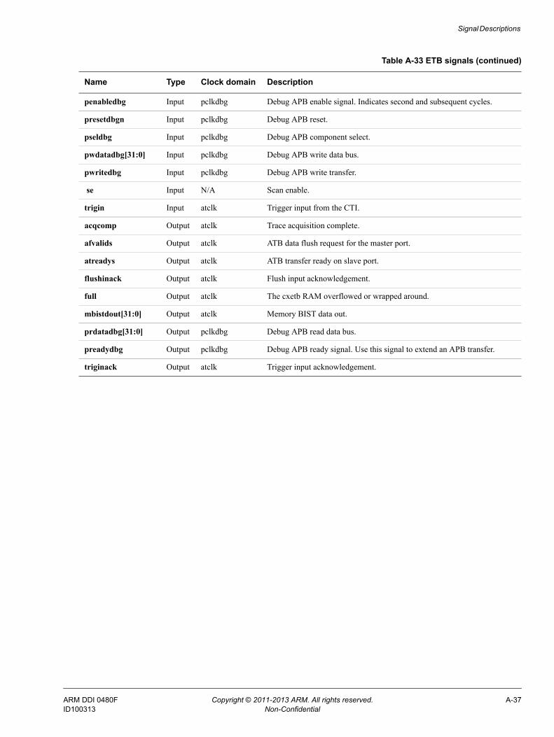
Signal Descriptions
penabledbg Input pclkdbg Debug APB enable signal. Indicates second and subsequent cycles.
presetdbgn Input pclkdbg Debug APB reset.
pseldbg Input pclkdbg Debug APB component select.
pwdatadbg[31:0] Input pclkdbg Debug APB write data bus.
pwritedbg Input pclkdbg Debug APB write transfer.
se Input N/A Scan enable.
trigin Input atclk Trigger input from the CTI.
acqcomp Output atclk Trace acquisition complete.
afvalids Output atclk ATB data flush request for the master port.
atreadys Output atclk ATB transfer ready on slave port.
flushinack Output atclk Flush input acknowledgement.
full Output atclk The cxetb RAM overflowed or wrapped around.
mbistdout[31:0] Output atclk Memory BIST data out.
prdatadbg[31:0] Output pclkdbg Debug APB read data bus.
preadydbg Output pclkdbg Debug APB ready signal. Use this signal to extend an APB transfer.
triginack Output atclk Trigger input acknowledgement.
Table A-33 ETB signals (continued)
Name Type Clock domain Description
ARM DDI 0480F Copyright © 2011-2013 ARM. All rights reserved. A-37ID100313 Non-Confidential

Signal Descriptions
A.7 Authentication and event bridgesThis section describes the following component signals:• Authentication asynchronous bridge signals.• Authentication synchronous bridge signals on page A-39.• Authentication replicator on page A-39.
A.7.1 Authentication asynchronous bridge signals
Table A-34 shows the authentication asynchronous bridge signals.
Cross-domain connections
The authentication asynchronous bridge can be configured as a separate master interface component and slave interface component. If you configure the bridge in this way, then you must connect the two components as Table A-35 shows.
Table A-35 shows authentication asynchronous bridge cross-domain connections.
Table A-34 Authentication asynchronous bridge signals
Name Type Clock domain Description
clks Input clks Authentication clock.
clkm Input clkm Authentication clock.
resetsn Input clks Authentication reset.
resetmn Input clkm Authentication reset.
dbgens Input clks Invasive debug enable.
nidens Input clks Non-invasive debug enable.
spidens Input clks Secure invasive debug enable.
spnidens Input clks Secure non-invasive debug enable.
dbgswens Input clks Invasive software debug enable.
dbgenm Output clkm Invasive debug enable.
nidenm Output clkm Non-invasive debug enable.
spidenm Output clkm Secure invasive debug enable.
spnidenm Output clkm Secure non-invasive debug enable.
dbgswenm Output clkm Invasive software debug enable.
Table A-35 Authentication asynchronous bridge cross-domain connections
Slave component signal Type Master component signal Type
authm_req_async Output auths_req_async Input
authm_ack_async Input auths_ack_async Output
authm_fwd_data_async Output auths_fwd_data_async Input
ARM DDI 0480F Copyright © 2011-2013 ARM. All rights reserved. A-38ID100313 Non-Confidential

Signal Descriptions
A.7.2 Authentication synchronous bridge signals
Table A-36 shows the authentication synchronous bridge signals.
A.7.3 Authentication replicator
Table A-37 shows the authentication replicator signals.
Table A-36 Authentication synchronous bridge signals
Name Type Clock domain Description
clk Input clk Authentication clock.
resetn Input clk Authentication reset.
dbgens Input clk Invasive debug enable.
nidens Input clk Non-invasive debug enable.
spidens Input clk Secure invasive debug enable
dbgswens Input clk Invasive software debug enable.
spnidens Input clk Secure non-invasive debug enable.
dbgenm Output clk Invasive debug enable.
nidenm Output clk Non invasive debug enable.
spidenm Output clk Secure invasive debug enable.
spnidenm Output clk Secure non-invasive debug enable.
dbgswenm Output clk Invasive software debug enable.
Table A-37 Authentication replicator signals
Name Type Clock domain Description
clk Input clk Authentication clock.
resetn Input clk Authentication reset.
dbgens Input clk Invasive debug enable.
nidens Input clk Non-invasive debug enable.
spidens Input clk Secure invasive debug enable.
spnidens Input clk Secure non-invasive debug enable.
dbgswens Input clk Invasive software debug enable.
dbgenm<x>a
a. Where <x> is the master interface number.
Output clk Invasive debug enable.
nidenm<x>a Output clk Non-invasive debug enable.
spidenm<x>a Output clk Secure invasive debug enable.
spnidenm<x>a Output clk Secure non-invasive debug enable.
dbgswenm<x>a Output clk Invasive software debug enable.
ARM DDI 0480F Copyright © 2011-2013 ARM. All rights reserved. A-39ID100313 Non-Confidential

Signal Descriptions
A.8 Granular power requestor signalsTable A-38 shows the granular power requestor signals.
Table A-38 Granular power requestor signals
Name Type Clock domain Description
clk Input clk Clock
resetn Input clk Reset
paddr31dbg Input clk Enables components to distinguish between internal accesses from system software and external accesses from a debugger.
cpwrupack[31:0] Input clk Powerup acknowledge. This signal acknowledges that a system power controller responded to a powerup or powerdown request.
pseldbg Input clk DAP select.
penabledbg Input clk DAP enable.
pwritedbg Input clk DAP write or read.
paddrdbg[11:2] Input clk DAP compressed address bus.
pwdatadbg[31:0] Input clk DAP write data bus.
preadydbg Output clk DAP ready.
pslverrdbg Output clk DAP slave error.
prdatadbg[31:0] Output clk DAP compressed address bus.
cpwrupreq[31:0] Output clk Powerup request. This signal requests the system power controller to:• Powerup the target power domain.• Enable the clocks.De-asserting cpwrupreq indicates to a power controller that power can be removed from a domain.
ARM DDI 0480F Copyright © 2011-2013 ARM. All rights reserved. A-40ID100313 Non-Confidential

Appendix B Revisions
This appendix describes the technical changes between released issues of this book.
Table B-1 Issue A
Change Location Affects
First release - -
Table B-2 Differences between Issue A and Issue B
Change Location Affects
Correction to signal name capitalization and signal directions. Chapter 2 Functional Overview All revisions
Correction to signal name capitalization and signal directions. Appendix A Signal Descriptions All revisions
Clarification of management register description. Chapter 3 Programmers Model All revisions
Component revision updated in the identification registers. Chapter 3 Programmers Model r1p0
ATB replicator IDFILTER0 diagram updated. Figure 3-52 on page 3-53 All revisions
Moved and updated DAPBUS interconnect and APB interconnect and ROM table chapters into subsections of the Debug Access Port.
Chapter 4 Debug Access Port All revisions
Component versions updated in block summary. CoreSight SoC-400 block summary on page 1-3
r1p0 and above
Detail added on clock domain crossing bridges. Chapter 4 Debug Access Port All revisions
Detail added on clock domain crossing bridges. Chapter 6 ATB Interconnect Components All revisions
ARM DDI 0480F Copyright © 2011-2013 ARM. All rights reserved. B-1ID100313 Non-Confidential

Revisions
Detail added on clock domain crossing bridges. Chapter 7 Timestamp Components All revisions
Event Asynchronous Bridge component information included. Entire document All revisions
Granular Power Requestor component added and referenced in Granular Power Requestor on page 2-30 and Granular power requestor signals on page A-40.
Chapter 11 Granular Power Requestor r1p0 and above
Timestamp interpolator component added and referenced in Timestamp interpolator on page 2-22 and Timestamp interpolator signals on page A-31.
Timestamp interpolator on page 7-11 r1p0 and above
Table B-3 Differences between Issue B and Issue C
Change Location Affects
Updated Structure of CoreSight SoC-400 on page 1-2 section. Chapter 1 Introduction All revisions
Updated Narrow timestamp asynchronous bridge revision in CoreSight SoC-400 block summary on page 1-3.
Chapter 1 Introduction All revisions
Updated Product revisions on page 1-13 for r2p0. Chapter 1 Introduction r2p0
Added rombaseaddrl[31:0] and rombaseaddru[31:0] to Figure 2-6 on page 2-6.
Chapter 2 Functional Overview All revisions
Added rombaseaddr[31:0] to Figure 2-7 on page 2-7. Chapter 2 Functional Overview All revisions
Updated Event asynchronous bridge on page 2-25 section. Chapter 2 Functional Overview All revisions
Moved and updated JTAG-DP register summary on page 3-173 into subsection of the Debug port register summary on page 3-173.
Chapter 3 Programmers Model All revisions
Moved and updated JTAP-DP register descriptions on page 3-202 into subsection of the Debug port implementation-specific registers on page 3-192.
Chapter 3 Programmers Model All revisions
Reset value correction in JTAG-DP register summary on page 3-173. Chapter 3 Programmers Model All revisions
Updated the description in Table 3-218 on page 3-181. Chapter 3 Programmers Model All revisions
Updated the description in Table 3-229 on page 3-190. Chapter 3 Programmers Model All revisions
Component revision updated in the identification registers. Chapter 3 Programmers Model r2p0
Updated DAP flow of control on page 4-3 section. Chapter 4 Debug Access Port All revisions
Moved and updated Operation in JTAG-DP mode on page 4-6 and Operation in SW-DP mode on page 4-7 into subsection of the JTAG and SWD interface on page 4-6.
Chapter 4 Debug Access Port All revisions
Updated ATB upsizer on page 6-6 section. Chapter 6 ATB Interconnect Components All revisions
Updated Arbitration on page 6-3 section in ATB funnel on page 6-3. Chapter 6 ATB Interconnect Components All revisions
Added rombaseaddrl[31:0] and rombaseaddru[31:0] to Table A-7 on page A-9.
Appendix A Signal Descriptions All revisions
Added rombaseaddr[31:0] to Table A-8 on page A-11. Appendix A Signal Descriptions All revisions
Table B-2 Differences between Issue A and Issue B (continued)
Change Location Affects
ARM DDI 0480F Copyright © 2011-2013 ARM. All rights reserved. B-2ID100313 Non-Confidential

Revisions
Table B-4 Differences between Issue C and Issue D
Change Location Affects
Updated the signal case for the following block diagrams:• Figure 2-25 on page 2-24.• Figure 2-26 on page 2-25.• Figure 2-28 on page 2-26.• Figure 2-29 on page 2-27.
Chapter 2 Functional Overview All
Updated the offset value for CIDR 0-3 in Table 3-246 on page 3-203 Chapter 3 Programmers Model All
Updated the top-level signal case for ECT components. Chapter 8 Embedded Cross Trigger All
Updated the top-level signal case for TPIU components. Chapter 9 Trace Port Interface Unit All
Updated the top-level signal case for ETB components. Chapter 10 Embedded Trace Buffer All
Updated the top-level signal case for ECT, TPIU, and ETB components.
Appendix A Signal Descriptions All
Updated the component version references Table 1-1 on page 1-3Table 3-51 on page 3-47
All
Table B-5 Differences between Issue D and Issue E
Change Location Affects
Updated product name to CoreSight SoC-400 Entire document All
Added compliance information Compliance on page 1-6 All
Updated signals Figure 2-6 on page 2-6 All
Updated Debug Base Register descriptions • AHB-AP Debug Base Address register, ROM, 0xF8 on page 3-181
• AXI-AP Debug Base Address register on page 3-187• APB-AP Debug Base Address register, BASE, 0xF8
on page 3-192
All
Updated reset value for DOMAIN field AXI-AP Control/Status Word register on page 3-182 r3p0
Updated figure to show JTAG-DP Figure 3-217 on page 3-196 All
Modified the revision value in AHB-AP Identification register
Table 3-219 on page 3-182 r3p0
Added a note for Domain field in AXI-AP CSW register Table 3-220 on page 3-183 r3p0
Updated ARLOCK and AWLOCK sizes AXI transfers on page 4-23 All
Added synchronization request signals • Table A-14 on page A-18• Table A-15 on page A-19• Table A-20 on page A-23
All
ARM DDI 0480F Copyright © 2011-2013 ARM. All rights reserved. B-3ID100313 Non-Confidential

Revisions
Table B-6 Differences between Issue E and Issue F
Change Location Affects
Corrected case of signals. Throughout All
Updated the component block versions. Chapter 1 IntroductionChapter 3 Programmers Model
r3p1
Updated the example CoreSight SoC-400 system. Typical CoreSight SoC-400 system on page 1-4 All
Improved clarity of the introduction. Chapter 1 Introduction All
Improved clarity of component descriptions in the functional overview, and redistributed information between this document, the ARM® CoreSight™ SoC-400 Integration Manual, and the ARM® CoreSight™ SoC-400 Implementation Guide to better match the intended audience of each document.
Chapter 2 Functional Overview All
Moved APB component descriptions from DAP component descriptions to their own sections and chapter.
Chapter 2 Functional OverviewChapter 4 Debug Access PortChapter 5 APB Interconnect ComponentsAppendix A Signal Descriptions
All
Moved event asynchronous bridge description from authentication bridges to cross-triggering components.
Chapter 2 Functional OverviewChapter 8 Embedded Cross TriggerAppendix A Signal Descriptions
All
Changed dapaddr[7:2] to dapcaddr[7:2]. AXI access port on page 2-5DAP AXI access port signals on page A-9
r3p1
Removed ts_bit_valid_qualify signal from narrow timestamp replicator.
Narrow timestamp replicator on page 2-20Narrow timestamp replicator on page 7-6Narrow timestamp replicator signals on page A-27
r3p1
Corrected timestamp interpolator signal list. Timestamp interpolator on page 2-22Timestamp interpolator signals on page A-31
All
Added description of the authentication replicator. Authentication bridges on page 2-28Authentication and event bridges on page A-38
All
Improved clarity of various programmers model registers. Chapter 3 Programmers Model All
Replaced SW-DP description of IDCODE register with DPIDR Register.
Debug port implementation-specific registers on page 3-192
All
Renamed SW-DP WCR Register to DLCR Register. Debug port implementation-specific registers on page 3-192
All
Added description of Timestamp generator CNTCVL and CNTCVU registers.
Timestamp generator registers description on page 3-205
All
Reorganized, consolidated and rewrote substantial information in the component description chapters to improve clarity.
Chapter 4 Debug Access PortChapter 5 APB Interconnect ComponentsChapter 6 ATB Interconnect ComponentsChapter 7 Timestamp ComponentsChapter 8 Embedded Cross TriggerChapter 9 Trace Port Interface UnitChapter 10 Embedded Trace Buffer
All
ARM DDI 0480F Copyright © 2011-2013 ARM. All rights reserved. B-4ID100313 Non-Confidential

Revisions
Added and corrected information on clocks and resets for each component. Described where synchronizers are required. Added note to consult the ARM® CoreSight™ SoC-400 Integration Manual, when using clock enables to interface between synchronous clock domains.
Chapter 4 Debug Access PortChapter 5 APB Interconnect ComponentsChapter 6 ATB Interconnect ComponentsChapter 7 Timestamp ComponentsChapter 8 Embedded Cross TriggerChapter 9 Trace Port Interface UnitChapter 10 Embedded Trace Buffer
All
Clarified the behavior of low power interfaces. Chapter 5 APB Interconnect ComponentsChapter 6 ATB Interconnect ComponentsChapter 7 Timestamp Components
All
Renamed SProt to CSW.Prot[1], because SProt is not defined elsewhere.
Chapter 4 Debug Access PortChapter 5 APB Interconnect ComponentsChapter 6 ATB Interconnect Components
All
Corrected arbitration behavior of the non-programmable funnel. Non-programmable funnel on page 6-5 All
Described use of ATB synchronous bridge as a trace buffer. ATB synchronous bridge on page 6-10 All
Described usage of the timestamp distribution network for processor time and CoreSight time, and clarified that the same network must not be used for both.
Chapter 7 Timestamp Components All
Clarified usage of the timestamp generator hltdbg signal. Timestamp generator on page 7-3 All
Updated guidance to TPA designers on traceclk alignment expectations.
traceclk alignment on page 9-5 All
Added flowcharts from CoreSight Design Kits explaining ETB trace stop, flush, and trigger operation.
ETB trace capture and formatting on page 10-5 All
Removed Granular Power Requestor chapter from the book, because the information is provided in Granular Power Requestor on page 2-30 and other sections.
Chapter 2 Functional Overview All
Corrected CTM signal list to show that its channel interfaces are always four channels wide.
CTM signals on page A-33 All
Listed signals that must be connected between slave and master interface components of asynchronous bridges when separately implemented
Appendix A Signal Descriptions All
Table B-6 Differences between Issue E and Issue F (continued)
Change Location Affects
ARM DDI 0480F Copyright © 2011-2013 ARM. All rights reserved. B-5ID100313 Non-Confidential