2
Surface Structure of Hydrogen Annealed Silicon Wafer using Ozonized Water and Dilute HF Cleaning Hisatsugu Kurita, Koji Izunome, Hiromi Nagahama, Takao Ino *) , Jyunsei Yamabe *) , Naoaki Sakurai *) Manufacturing Technology Department, Silicon Division, Toshiba Ceramics Co., Ltd. 6-861-5, Higashikou, Sheirou-machi, Kitakanbara-Gun, Niigata, 957-0197, Japan *) Manufacturing Technology Center, Toshiba Corporation 33 Shin-Isogo, Isogo-ku, Yokohama-City, Kanagawa, 235-0017, Japan 1. Introduction The control of surface structure in silicon (Si) wafers is one of the most important factors in developing the performance of MOS LSI. The surface roughness has been affected the thickness uniformity of dielectric oxide-film on Si wafer. Hydrogen annealed Czochralski-grown (CZ) Si have periodic structure consisting of terraces and atomic-steps. (1,2) Yanase et al. (3) reported the surface structure was preserved after SC-1 (NH 4 OH/H 2 O 2 /H 2 O) cleaning although micro- roughness on the surface increased because of anisotropic Si etching in alkaline solution. (4) No report has been made, however, on the effect of ozonized water and dilute HF (DHF) cleaning on the variation of the surface structure for hydrogen annealed Si wafer. In this work, we studied the oxidation and etching of Si surface in ozonized water and DHF cleaning. 2. Experimental Polished wafers used in this study were boron- doped CZ-Si (100) (200 mm in diameter) with a mis- orientation angle of 0.04 or less toward <100> direction, a resistivity of 1 ohm-cm and a oxygen concentration of 9x10 17 atoms/cm 3 . These wafers were annealed in hydrogen atmosphere at 1200 degree C for 1 hour, using a commercial-available vertical furnace. To understand the variation of surface structure before and after cleaning, hydrogen annealed wafers were treated by two kinds of cleaning as follows: (1) Repetitive single-wafer spin cleaning with 20ppm-ozonized water for 30sec and successively 1% HF for 20 sec (O 3 /DHF cleaning). (2) Immersion-type wet cleaning with a modified SC-1 solution (NH 4 : H 2 O 2 : H 2 O= 1: 4: 25 at 70 degrees) for 10 min (SC-1 cleaning). The wafers were observed surface structure used AFM (Nanoscpoe III) with an area of 1x1μm 2 . Etching depth from Si surface was calculated by the variation of poly-Si film on Si before and after cleaning. To clarify the oxidation mechanism, we prepared boron-doped CZ-Si (100) and Si (111) (200 mm in diameter) with a resistivity of 1 ohm-cm. The wafers were treated in 20ppm-ozonized water between 0 and 30seconds. Thickness of chemical oxides films on hydrogen annealing wafers was measured using X-ray Photoelectron Spectroscopy(XPS). 3. Results and Discussion The typical AFM images of as-annealed, after O 3 /DHF cleaning and SC-1 cleaning are shown in Fig.1. The periodic structure consisting of the terraces with 0.7-1.0 μm widths and single-atomic layer step (0.15 nm) remains after both cleaning. Surface roughness (Rms) values of O 3 /DHF cleaning and SC-1 cleaning are 0.11 nm and 0.16 nm, respectively. The microstructure of terraces with 80-90 nm and single- atomic layer step clearly remains after O 3 /DHF cleaning as shown in Fig. 1. Etching depth from surface after O 3 /DHF cleaning and SC-1 cleaning are calculated as 2.6 nm and 1.5 nm, respectively. Thus, it is found that Si etching from surface after O 3 /DHF cleaning is more uniform than that after SC-1 cleaning. Fig. 2 shows the thickness of chemical oxide on Si (100) and Si (111) wafer surfaces using XPS as a function of ozonized water application time in O 3 /DHF cleaning. Increasing thickness of chemical oxide on Si (100) and Si (111) increases with ozonized water application time. Si oxidation in ozonized water has isotropic property in Fig.2. Therefore, it is found that the surface on annealed Si wafer after O 3 /DHF cleaning become smoother feature than that after SC-1 cleaning. 4. Conclusion The surface structure, consisting of terraces and atomic-steps on hydrogen annealed Si wafer was evaluated by AFM after O 3 /DHF cleaning and modified SC-1 cleaning. It has been found that surface microstructure after O 3 /DHF cleaning preserve clearly rather than that after SC-1 cleaning. It suggests that Si oxidation in ozonized water have isotropic property. The O 3 /DHF cleaning is, thus, effective process on hydrogen annealed Si wafer surface. References 1. K. Izunome, Y. Saito and H. Kubota, Jpn. J. Appl. Phys., 31, L1277 (1992). 2. L. Zhong et al., Appl. Phys. Lett., 68, 1823 (1996). 3. Y. Yanase et al., J. Electrochem. Soc.141,325(1994) 4. F. Shimura, “Semiconductor Silicon Crystal Technology” (Academic Press, 1989) p.49. Fig.1 AFM images (1 1μm 2 ) of a Si (100) surface tilted toward <100> direction by 0.04 or less after H 2 annealing (a), after O 3 /DHF cleaning (b), after SC-1 cleaning (c), showing aperiodic structure in the [110] direction Fig.2 Thickness of chemical oxide on Si (111) wafer and Si (100) wafer surface measured XPS as a function of ozonized water application time 0.0 0.1 0.2 0.3 0.4 0.5 0.6 0.7 0.8 0.9 1.0 0 10 20 30 40 Ozonized water application time / sec Thickness of chemical oxide on Si surface / nm (111) (100) [110] (a) (b) (c)

are 0.11 nm and 0.16 nm, respectively. The microstructure ... · Surface Structure of Hydrogen Annealed Silicon W afer using Ozonized W ater and Dilute HF Cleaning Hisatsugu Kurita,

Embed Size (px)

Citation preview

Surface Structure of Hydrogen Annealed Silicon Wafer using Ozonized Water and Dilute HF Cleaning

Hisatsugu Kurita, Koji Izunome, Hiromi Nagahama,

Takao Ino* ), Jyunsei Yamabe* ), Naoaki Sakurai* ) Manufacturing Technology Department, Silicon Division, Toshiba Ceramics Co., Ltd.

6-861-5, Higashikou, Sheirou-machi, Kitakanbara-Gun, Niigata, 957-0197, Japan

* )Manufacturing Technology Center, Toshiba Corporation 33 Shin-Isogo, Isogo-ku, Yokohama-City,

Kanagawa, 235-0017, Japan

1. Introduction The control of surface structure in silicon (Si)

wafers is one of the most important factors in developing the performance of MOS LSI. The surface roughness has been affected the thickness uniformity of dielectric oxide-film on Si wafer. Hydrogen annealed Czochralski-grown (CZ) Si have periodic structure consisting of terraces and atomic-steps. (1,2) Yanase et al. (3) reported the surface structure was preserved after SC-1 (NH4OH/H2O2/H2O) cleaning although micro-roughness on the surface increased because of anisotropic Si etching in alkaline solution. (4) No report has been made, however, on the effect of ozonized water and dilute HF (DHF) cleaning on the variation of the surface structure for hydrogen annealed Si wafer. In this work, we studied the oxidation and etching of Si surface in ozonized water and DHF cleaning.

2. Experimental Polished wafers used in this study were boron-

doped CZ-Si (100) (200 mm in diameter) with a mis-orientation angle of 0.04 or less toward <100> direction, a resistivity of 1 ohm-cm and a oxygen concentration of 9x10¹⁷ atoms/cm3. These wafers were annealed in hydrogen atmosphere at 1200 degree C for 1 hour, using a commercial-available vertical furnace. To understand the variation of surface structure before and after cleaning, hydrogen annealed wafers were treated by two kinds of cleaning as follows:

(1) Repetitive single-wafer spin cleaning with 20ppm-ozonized water for 30sec and successively 1% HF for 20 sec (O3/DHF cleaning).

(2) Immersion-type wet cleaning with a modified SC-1 solution (NH4: H2O2: H2O= 1: 4: 25 at 70 degrees) for 10 min (SC-1 cleaning).

The wafers were observed surface structure used AFM (Nanoscpoe III) with an area of 1x1µm2. Etching depth from Si surface was calculated by the variation of poly-Si film on Si before and after cleaning.

To clarify the oxidation mechanism, we prepared boron-doped CZ-Si (100) and Si (111) (200 mm in diameter) with a resistivity of 1 ohm-cm. The wafers were treated in 20ppm-ozonized water between 0 and 30seconds. Thickness of chemical oxides films on hydrogen annealing wafers was measured using X-ray Photoelectron Spectroscopy(XPS).

3. Results and Discussion The typical AFM images of as-annealed, after

O3/DHF cleaning and SC-1 cleaning are shown in Fig.1. The periodic structure consisting of the terraces with 0.7-1.0 µm widths and single-atomic layer step (0.15 nm) remains after both cleaning. Surface roughness (Rms) values of O3/DHF cleaning and SC-1 cleaning

are 0.11 nm and 0.16 nm, respectively. The microstructure of terraces with 80-90 nm and single-atomic layer step clearly remains after O3/DHF cleaning as shown in Fig. 1. Etching depth from surface after O3/DHF cleaning and SC-1 cleaning are calculated as 2.6 nm and 1.5 nm, respectively. Thus, it is found that Si etching from surface after O3/DHF cleaning is more uniform than that after SC-1 cleaning.

Fig. 2 shows the thickness of chemical oxide on Si (100) and Si (111) wafer surfaces using XPS as a function of ozonized water application time in O3/DHF cleaning. Increasing thickness of chemical oxide on Si (100) and Si (111) increases with ozonized water application time. Si oxidation in ozonized water has isotropic property in Fig.2. Therefore, it is found that the surface on annealed Si wafer after O3/DHF cleaning become smoother feature than that after SC-1 cleaning.

4. Conclusion The surface structure, consisting of terraces and

atomic-steps on hydrogen annealed Si wafer was evaluated by AFM after O3/DHF cleaning and modified SC-1 cleaning. It has been found that surface microstructure after O3/DHF cleaning preserve clearly rather than that after SC-1 cleaning. It suggests that Si oxidation in ozonized water have isotropic property. The O3/DHF cleaning is, thus, effective process on hydrogen annealed Si wafer surface.

References 1. K. Izunome, Y. Saito and H. Kubota, Jpn. J. Appl.

Phys., 31, L1277 (1992). 2. L. Zhong et al., Appl. Phys. Lett., 68, 1823 (1996). 3. Y. Yanase et al., J. Electrochem.

Soc.141,325(1994) 4. F. Shimura, “Semiconductor Silicon Crystal

Technology” (Academic Press, 1989) p.49.

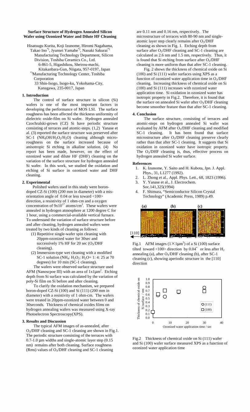
Fig.1 AFM images (1�

1µm2) of a Si (100) surface tilted toward <100> direction by 0.04 or less after H2 annealing (a), after O3/DHF cleaning (b), after SC-1 cleaning (c), showing aperiodic structure in the [110] direction

Fig.2 Thickness of chemical oxide on Si (111) wafer and Si (100) wafer surface measured XPS as a function of ozonized water application time

0.00.10.20.30.40.50.60.70.80.91.0

0 10 20 30 40Ozonized water application time / sec

Thi

ckne

ss o

f ch

emic

al o

xide

on

Si s

urfa

ce /

nm

(111)

(100)

[110]

(a) (b) (c)