Embed Size (px)
Citation preview
[Sumy, 4(10): October, 2015] ISSN: 2277-9655
(I2OR), Publication Impact Factor: 3.785
http: // www.ijesrt.com© International Journal of Engineering Sciences & Research Technology
[765]
IJESRT INTERNATIONAL JOURNAL OF ENGINEERING SCIENCES & RESEARCH
TECHNOLOGY
INTEGRATED BUCK–FLYBACK NON ISOLATED PFC CONVERTER WITH
CONSTANT ON-TIME CONTROL Sumy P S
* M.Tech, Power Electronics, NSS College of Engineering Palakkad, India
ABSTRACT
An integrated buck–flyback non isolated power factor correction converter is proposed in this paper. This new
converter is an inherent integration of a buck converter and a flyback converter, which operates in either flyback
mode or buck mode according to whether the input voltage is lower or higher than the output voltage. In this way,
the dead zones of ac input current in traditional buck power factor correction converter can be eliminated. Therefore,
the proposed integrated buck–flyback power factor correction converter can achieve high power factor under
universal ac input range, and its input current harmonics can be reduced. Conventional Buck power factor correction
converter and proposed converter are simulated using MATLAB/Simulink. A 10W laboratory prototype of the
proposed power factor correction converter with 12V input voltage was setup using PIC 16F877 microcontroller.
Compared to conventional power factor correction converters, the power factor was improved greatly with the
proposed topology especially at low line. This proposed topology is very suitable for high-power non isolated LED
drivers with high power factor requirements.
KEYWORDS: AC–DC Converter, Buck–flyback converter, Harmonic currents, Constant On Time(COT)control,
High power factor (PF).
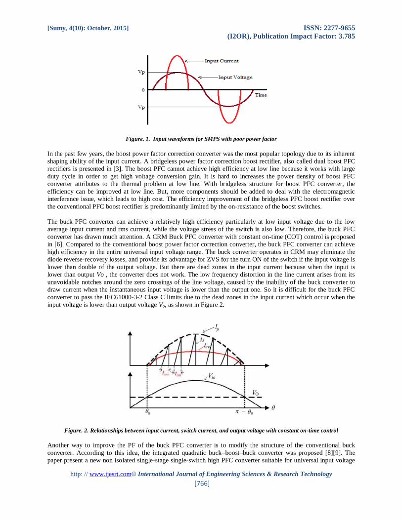
INTRODUCTION AC/DC converter plays a major role in day to-day life. Electrical energy is almost exclusively generated, transmitted
and distributed in the form of alternating current. Therefore the question of power factor immediately comes into
picture. In recent years, the power electronic systems and devices, which are used more frequently, create harmonic
current and pollute the electricity network. Harmonics have a negative effect on the operation of the receiver, which
is fed from the same network. AC-DC converters have drawbacks of poor power quality in terms of injected current
harmonics, which cause voltage distortion and poor power factor at input ac mains and slow varying ripples at dc
output load, low efficiency and large size of AC- DC filters. SMPS, the most frequently used power electronic
system, can present nonlinear loads which impose current harmonics onto the main power network. Awareness of
the necessity of power quality is increasing, and power factor correction is being implemented on a growing scale.
Power factor correction technique is well applied to the ac/dc converters because it can provide almost sinusoidal
input current. Because we want a constant dc supply in the output, so we connect a capacitor in the output of ac/dc
converters. This capacitor distorts the input current waveform. To overcome these drawbacks, low harmonic and
high power factor converters are used. We replaced the single AC-DC rectifier by a rectifier followed by a DC-DC
power factor correction.
[Sumy, 4(10): October, 2015] ISSN: 2277-9655
(I2OR), Publication Impact Factor: 3.785
http: // www.ijesrt.com© International Journal of Engineering Sciences & Research Technology
[766]
Figure. 1. Input waveforms for SMPS with poor power factor
In the past few years, the boost power factor correction converter was the most popular topology due to its inherent
shaping ability of the input current. A bridgeless power factor correction boost rectifier, also called dual boost PFC
rectifiers is presented in [3]. The boost PFC cannot achieve high efficiency at low line because it works with large
duty cycle in order to get high voltage conversion gain. It is hard to increases the power density of boost PFC
converter attributes to the thermal problem at low line. With bridgeless structure for boost PFC converter, the
efficiency can be improved at low line. But, more components should be added to deal with the electromagnetic
interference issue, which leads to high cost. The efficiency improvement of the bridgeless PFC boost rectifier over
the conventional PFC boost rectifier is predominantly limited by the on-resistance of the boost switches.
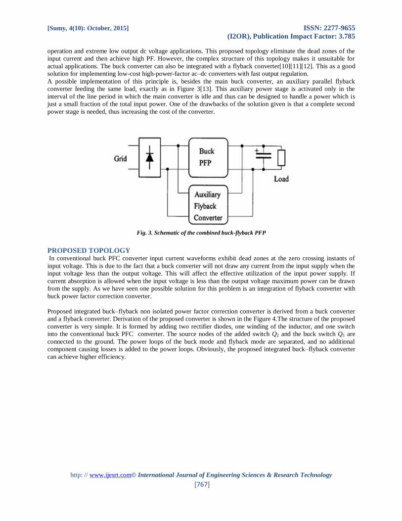
The buck PFC converter can achieve a relatively high efficiency particularly at low input voltage due to the low
average input current and rms current, while the voltage stress of the switch is also low. Therefore, the buck PFC
converter has drawn much attention. A CRM Buck PFC converter with constant on-time (COT) control is proposed
in [6]. Compared to the conventional boost power factor correction converter, the buck PFC converter can achieve
high efficiency in the entire universal input voltage range. The buck converter operates in CRM may eliminate the
diode reverse-recovery losses, and provide its advantage for ZVS for the turn ON of the switch if the input voltage is
lower than double of the output voltage. But there are dead zones in the input current because when the input is
lower than output Vo , the converter does not work. The low frequency distortion in the line current arises from its
unavoidable notches around the zero crossings of the line voltage, caused by the inability of the buck converter to
draw current when the instantaneous input voltage is lower than the output one. So it is difficult for the buck PFC
converter to pass the IEC61000-3-2 Class C limits due to the dead zones in the input current which occur when the
input voltage is lower than output voltage Vo, as shown in Figure 2.
Figure. 2. Relationships between input current, switch current, and output voltage with constant on-time control
Another way to improve the PF of the buck PFC converter is to modify the structure of the conventional buck
converter. According to this idea, the integrated quadratic buck–boost–buck converter was proposed [8][9]. The
paper present a new non isolated single-stage single-switch high PFC converter suitable for universal input voltage
[Sumy, 4(10): October, 2015] ISSN: 2277-9655
(I2OR), Publication Impact Factor: 3.785
http: // www.ijesrt.com© International Journal of Engineering Sciences & Research Technology
[767]
operation and extreme low output dc voltage applications. This proposed topology eliminate the dead zones of the
input current and then achieve high PF. However, the complex structure of this topology makes it unsuitable for
actual applications. The buck converter can also be integrated with a flyback converter[10][11][12]. This as a good
solution for implementing low-cost high-power-factor ac–dc converters with fast output regulation.
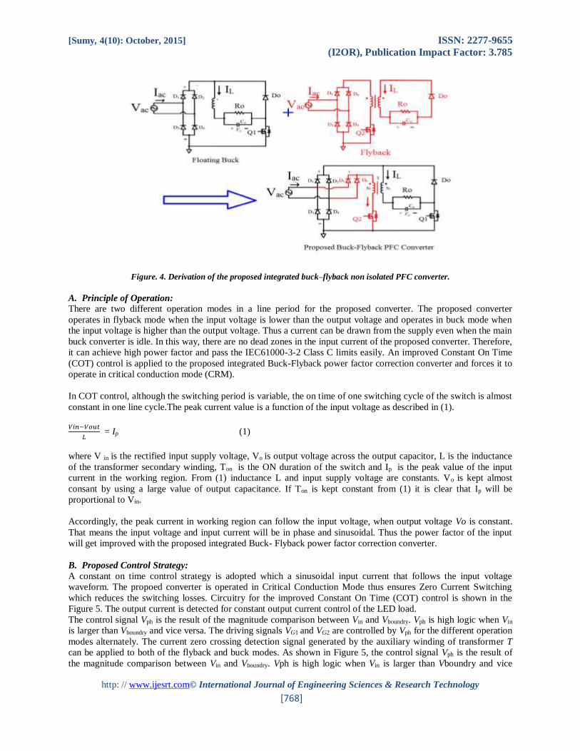
A possible implementation of this principle is, besides the main buck converter, an auxiliary parallel flyback
converter feeding the same load, exactly as in Figure 3[13]. This auxiliary power stage is activated only in the
interval of the line period in which the main converter is idle and thus can be designed to handle a power which is
just a small fraction of the total input power. One of the drawbacks of the solution given is that a complete second
power stage is needed, thus increasing the cost of the converter.
Fig. 3. Schematic of the combined buck-flyback PFP
PROPOSED TOPOLOGY In conventional buck PFC converter input current waveforms exhibit dead zones at the zero crossing instants of
input voltage. This is due to the fact that a buck converter will not draw any current from the input supply when the
input voltage less than the output voltage. This will affect the effective utilization of the input power supply. If
current absorption is allowed when the input voltage is less than the output voltage maximum power can be drawn
from the supply. As we have seen one possible solution for this problem is an integration of flyback converter with
buck power factor correction converter.
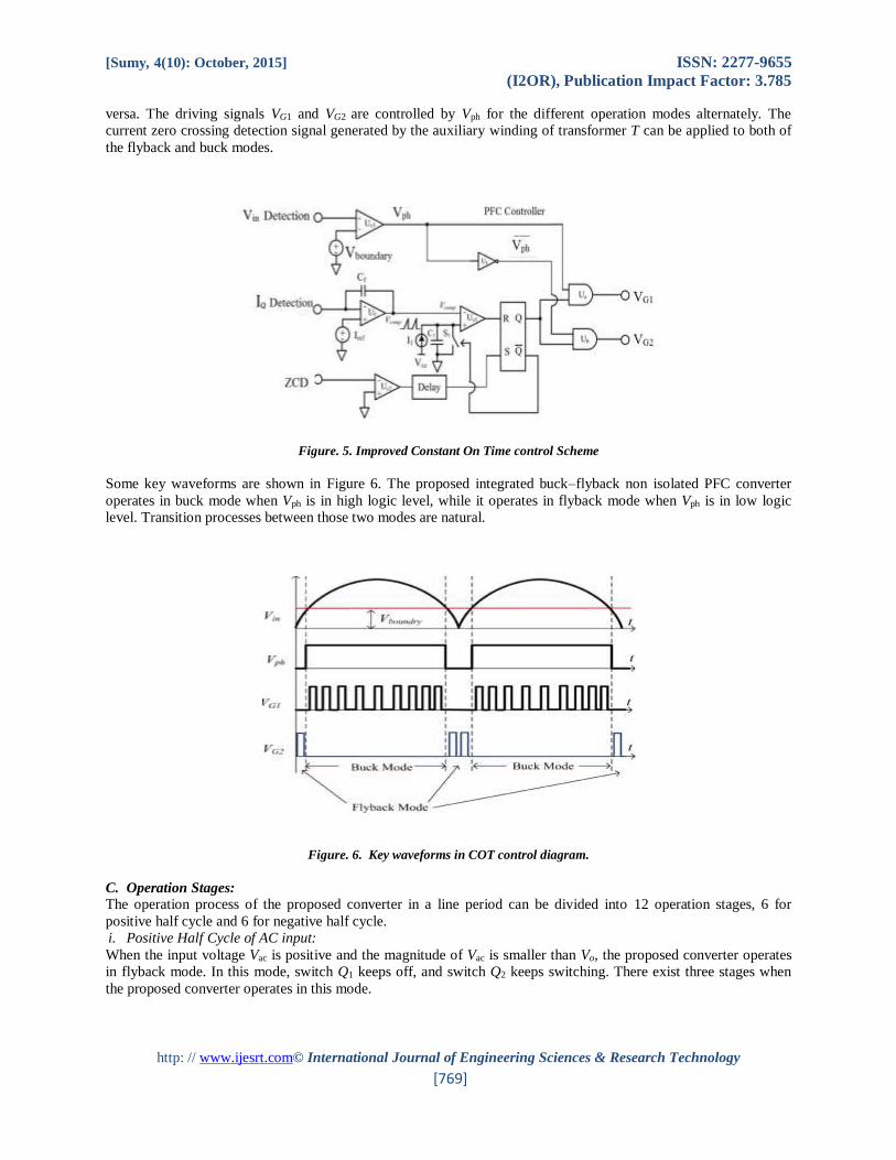
Proposed integrated buck–flyback non isolated power factor correction converter is derived from a buck converter
and a flyback converter. Derivation of the proposed converter is shown in the Figure 4.The structure of the proposed
converter is very simple. It is formed by adding two rectifier diodes, one winding of the inductor, and one switch
into the conventional buck PFC converter. The source nodes of the added switch Q2 and the buck switch Q1 are
connected to the ground. The power loops of the buck mode and flyback mode are separated, and no additional
component causing losses is added to the power loops. Obviously, the proposed integrated buck–flyback converter
can achieve higher efficiency.
[Sumy, 4(10): October, 2015] ISSN: 2277-9655
(I2OR), Publication Impact Factor: 3.785
http: // www.ijesrt.com© International Journal of Engineering Sciences & Research Technology
[768]
Figure. 4. Derivation of the proposed integrated buck–flyback non isolated PFC converter.
A. Principle of Operation:
There are two different operation modes in a line period for the proposed converter. The proposed converter
operates in flyback mode when the input voltage is lower than the output voltage and operates in buck mode when
the input voltage is higher than the output voltage. Thus a current can be drawn from the supply even when the main
buck converter is idle. In this way, there are no dead zones in the input current of the proposed converter. Therefore,
it can achieve high power factor and pass the IEC61000-3-2 Class C limits easily. An improved Constant On Time
(COT) control is applied to the proposed integrated Buck-Flyback power factor correction converter and forces it to
operate in critical conduction mode (CRM).
In COT control, although the switching period is variable, the on time of one switching cycle of the switch is almost
constant in one line cycle.The peak current value is a function of the input voltage as described in (1).
𝑉𝑖𝑛−𝑉𝑜𝑢𝑡
𝐿 = Ip (1)
where V in is the rectified input supply voltage, Vo is output voltage across the output capacitor, L is the inductance
of the transformer secondary winding, Ton is the ON duration of the switch and Ip is the peak value of the input
current in the working region. From (1) inductance L and input supply voltage are constants. Vo is kept almost
consant by using a large value of output capacitance. If Ton is kept constant from (1) it is clear that Ip will be
proportional to Vin.
Accordingly, the peak current in working region can follow the input voltage, when output voltage Vo is constant.
That means the input voltage and input current will be in phase and sinusoidal. Thus the power factor of the input
will get improved with the proposed integrated Buck- Flyback power factor correction converter.
B. Proposed Control Strategy:
A constant on time control strategy is adopted which a sinusoidal input current that follows the input voltage
waveform. The propoed converter is operated in Critical Conduction Mode thus ensures Zero Current Switching
which reduces the switching losses. Circuitry for the improved Constant On Time (COT) control is shown in the
Figure 5. The output current is detected for constant output current control of the LED load.
The control signal Vph is the result of the magnitude comparison between Vin and Vboundry. Vph is high logic when Vin
is larger than Vboundry and vice versa. The driving signals VG1 and VG2 are controlled by Vph for the different operation
modes alternately. The current zero crossing detection signal generated by the auxiliary winding of transformer T
can be applied to both of the flyback and buck modes. As shown in Figure 5, the control signal Vph is the result of
the magnitude comparison between Vin and Vboundry. Vph is high logic when Vin is larger than Vboundry and vice
[Sumy, 4(10): October, 2015] ISSN: 2277-9655
(I2OR), Publication Impact Factor: 3.785
http: // www.ijesrt.com© International Journal of Engineering Sciences & Research Technology
[769]
versa. The driving signals VG1 and VG2 are controlled by Vph for the different operation modes alternately. The
current zero crossing detection signal generated by the auxiliary winding of transformer T can be applied to both of
the flyback and buck modes.
Figure. 5. Improved Constant On Time control Scheme
Some key waveforms are shown in Figure 6. The proposed integrated buck–flyback non isolated PFC converter
operates in buck mode when Vph is in high logic level, while it operates in flyback mode when Vph is in low logic
level. Transition processes between those two modes are natural.
Figure. 6. Key waveforms in COT control diagram.
C. Operation Stages:
The operation process of the proposed converter in a line period can be divided into 12 operation stages, 6 for
positive half cycle and 6 for negative half cycle.
i. Positive Half Cycle of AC input:
When the input voltage Vac is positive and the magnitude of Vac is smaller than Vo, the proposed converter operates
in flyback mode. In this mode, switch Q1 keeps off, and switch Q2 keeps switching. There exist three stages when
the proposed converter operates in this mode.
[Sumy, 4(10): October, 2015] ISSN: 2277-9655
(I2OR), Publication Impact Factor: 3.785
http: // www.ijesrt.com© International Journal of Engineering Sciences & Research Technology
[770]
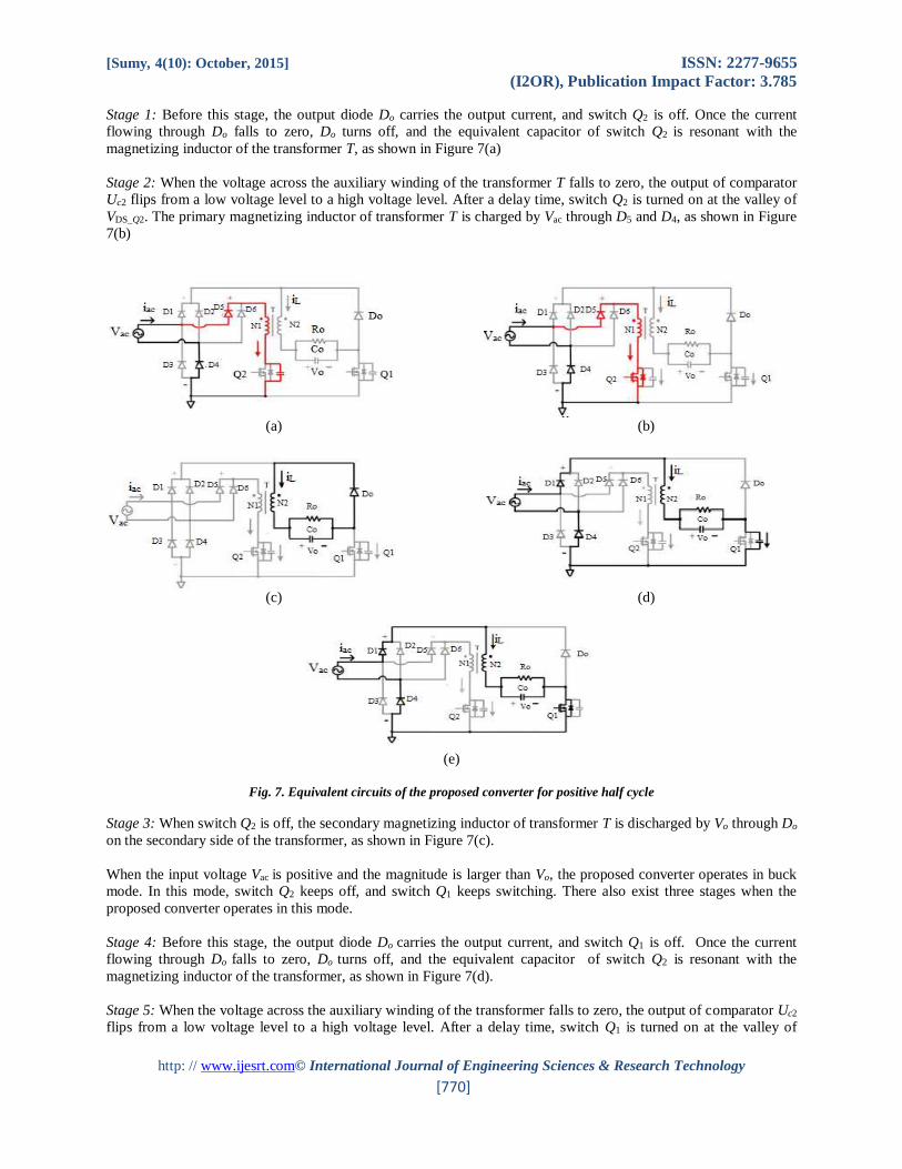
Stage 1: Before this stage, the output diode Do carries the output current, and switch Q2 is off. Once the current
flowing through Do falls to zero, Do turns off, and the equivalent capacitor of switch Q2 is resonant with the
magnetizing inductor of the transformer T, as shown in Figure 7(a)
Stage 2: When the voltage across the auxiliary winding of the transformer T falls to zero, the output of comparator
Uc2 flips from a low voltage level to a high voltage level. After a delay time, switch Q2 is turned on at the valley of
VDS_Q2. The primary magnetizing inductor of transformer T is charged by Vac through D5 and D4, as shown in Figure
7(b)
(a) (b)
(c) (d)
(e)
Fig. 7. Equivalent circuits of the proposed converter for positive half cycle
Stage 3: When switch Q2 is off, the secondary magnetizing inductor of transformer T is discharged by Vo through Do
on the secondary side of the transformer, as shown in Figure 7(c).
When the input voltage Vac is positive and the magnitude is larger than Vo, the proposed converter operates in buck
mode. In this mode, switch Q2 keeps off, and switch Q1 keeps switching. There also exist three stages when the
proposed converter operates in this mode.
Stage 4: Before this stage, the output diode Do carries the output current, and switch Q1 is off. Once the current
flowing through Do falls to zero, Do turns off, and the equivalent capacitor of switch Q2 is resonant with the
magnetizing inductor of the transformer, as shown in Figure 7(d).
Stage 5: When the voltage across the auxiliary winding of the transformer falls to zero, the output of comparator Uc2
flips from a low voltage level to a high voltage level. After a delay time, switch Q1 is turned on at the valley of
[Sumy, 4(10): October, 2015] ISSN: 2277-9655
(I2OR), Publication Impact Factor: 3.785
http: // www.ijesrt.com© International Journal of Engineering Sciences & Research Technology
[771]
VDS_Q1. The secondary magnetizing inductor of transformer T is charged by Vac − Vo through D1 and D4, as shown in
Figure 7(e).
Stage 6: When switch Q1 is off, the secondary magnetizing inductor of transformer T is discharged by Vo through Do
as shown in the Figure 7(c).
ii. Negative Half Cycle of AC Input:
When the input voltage Vac is negative, the proposed converter also operates in flyback mode and buck mode in
different input voltage regions. The operation processes in negative half-cycle of ac input can also be divided into
six operation stages, and the equivalent circuits are shown in Figure 8(a) to 8(d) The operation processes of the
proposed converter in the negative half-cycle of ac input are similar to those of the positive half-cycle.
(a) (b)
(b) (d)
Fig. 8. Equivalent circuits of the proposed converter for negative half cycle
DESIGN CONSIDERATIONS Input Current Analysis:
When the input voltage is lower than the output voltage in half line cycle, the buck converter does not work. The
conduction angle of the input current during buck mode equals (π − 2θ0 ). Assuming Vim is the amplitude of the line
voltage, then, angle θ0 is defined as
θ0 = arcsin(Vboundry/Vim)
θ0 = arcsin(Vo/Vim ) (1)
When the input voltage is higher than the output voltage, the buck converter begins working, and the slope of the
inductor current iLs for the buck operating region in half line cycle is given by the expression
LdiLs (t)/dt = Vim | sin(θ)| − Vo, θ∈ (θ0, π − θ0 ) (2)
where θ = ωl t and ωl = 2πfl is the line angular frequency. So, the peak value of the inductor current during switching
cycle during buck mode can be modified as follows:
Ipk1 (θ) =( Vim | sin(θ)| − Vo) Ton / Ls (3)

[Sumy, 4(10): October, 2015] ISSN: 2277-9655
(I2OR), Publication Impact Factor: 3.785
http: // www.ijesrt.com© International Journal of Engineering Sciences & Research Technology
[772]
where Ls in the secondary winding inductance and Ton is the on-time of the switch, which is almost constant during
half line cycle. The peak value of the inductor current during switching cycle during flyback mode can be written as
follows:
ipk2(θ) =(Vim.sin θ)Ton / Lp (4)
where Lp in the primary winding inductance
D(θ) = Vo / (Vim | sin(θ)|), θ∈ (θ0, π − θ0 ) (5)
Then, the average input current iav of the buck converter is determined as follows:
iav (θ) = Ipk1 (θ)D(θ) / 2 , θ∈ (θ0, π − θ0 ) (6)
Output Voltage Selection:
Within a half line cycle, the input current can flow only when the input voltage is greater than the output voltage. It
should be noted that the PF is affected by the output voltage significantly. With an increasing output voltage, the PF
decreases. Although lower output voltage results in higher PF, the efficiency of buck converter will decrease with
the decrease of output voltage at same load. The output voltage is preferred to be set around 80 V considering the
voltage stress of the output capacitor
Inductance Selection:
The input power Pin is calculated as follows:
Pin = 2
π∫ iav(θ)Vim. sinθ dθ
π/2
θ0 (7)
Assuming η is the efficiency of the converter, the output power Po can be expressed as follows:
Po =η.Pin= 2η
π∫
π/2
θ0iav(θ).Vim.sinθ dθ (8)
By substituting (6) into (8) we will get
Po=η.Pin = ηTon
πLs∫
π/2
θ0(Vin.sinθ- Vo).Vodθ (9)
During buck mode,
Toff(θ) = Ipk1(θ).L
Vo (10)
Switching frequency as a function of time is given by,
fs (θ) =1/(Ton + Toff (θ)) = Vo/(Ton.Vim sin(θ)) (11)
From (9) Ton can be expressed as
Ton = πLsPo
η
1
∫ (Vim.sinθ−Vo).Vo dθπ/2θ0
(12)
Combining (11) and (12),
fs = η.Vo2
π.Ls.Po.Vim.sinθ∫
𝜋/2
𝜃𝑜(Vim.sinθ –Vo) dθ, θo ≤ θ ≤ 𝜋 − 𝜃𝑜 (13)

[Sumy, 4(10): October, 2015] ISSN: 2277-9655
(I2OR), Publication Impact Factor: 3.785
http: // www.ijesrt.com© International Journal of Engineering Sciences & Research Technology
[773]
Obviously, the lowest frequency in half line cycle appears at θ = π/2. Therefore, the minimum frequency as a
function of input voltage Vim can be obtained when θ = π/2
fs-min = η.Vo2
π.Ls.Po.Vim−min∫
𝜋/2
𝜃𝑜(Vim-min sinθ – Vo) dθ (14)
Then, the transformer secondary winding inductance Ls is obtained as follows:
Ls = η.Vo2
π.fs−min.Po.Vim−min∫
𝜋/2
𝜃𝑜(Vim-min sinθ – Vo) dθ (15)
where Vim-min = 60. If the minimum switching frequency fs-min is assumed to be 10 kHz, output power is designed at
100W and the output voltage is designed at 60V. Then,
θo = arcsin (Vo/Vim)
where Vim is 100V. θo is obtained as,
θo= 0.2π
For an efficiency η of 0.96, the inductance is obtained as,
Ls=1 mH.
Lp/Ls = (N1/N2)2 (16)
where N1/N2 is the turns ratio which can be taken as n. Chosing n as 2.
Lp = 4 mH
Output Capacitance Selection:
Output capacitor is designed by the equation,
CfS
Of
Vf
IC
.8 (17)
where ΔVCf is usually considered as 5%–10% of the output voltage. This capacitor value is chosen to be higher than
the one given by the above equation and
Io = Po/Vo
Cf = 150 μF
SIMULATION RESULTS The performance of the proposed converter and the control strategy are evaluated by conducting the Simulation
analysis. MATLAB/Simulink version R2012a is used for simulation. The input given is 100 V and the parameters
are designed for a 100 W, 60V topology.
[Sumy, 4(10): October, 2015] ISSN: 2277-9655
(I2OR), Publication Impact Factor: 3.785
http: // www.ijesrt.com© International Journal of Engineering Sciences & Research Technology
[774]
Table 1. Simulation Parameters For Integrated
Buck- Flyback Converter
PARAMETER VALUE
Lp 1mH
Ls 4mH
Transformer Turns ratio, n 2
Output Capacitor, Co 150μF
Switch Q1, Q2 IRF 840
Diode Do 1N4007
Fig. 9. Proposed Converter Circuit
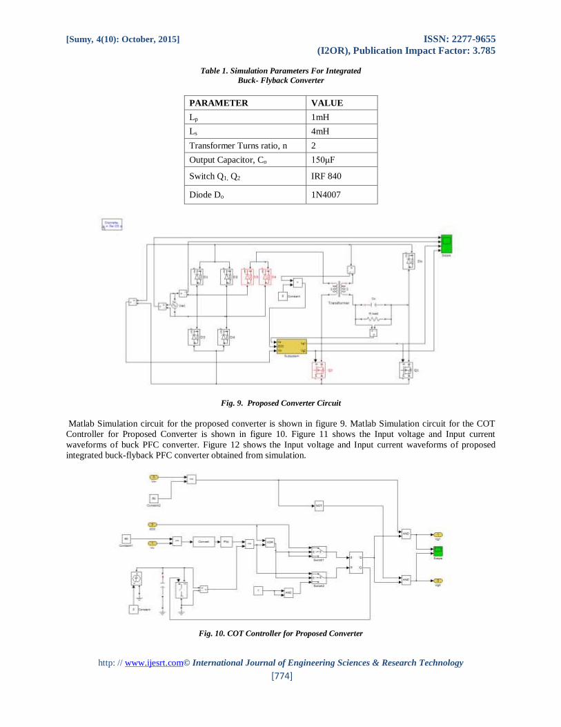
Matlab Simulation circuit for the proposed converter is shown in figure 9. Matlab Simulation circuit for the COT
Controller for Proposed Converter is shown in figure 10. Figure 11 shows the Input voltage and Input current
waveforms of buck PFC converter. Figure 12 shows the Input voltage and Input current waveforms of proposed
integrated buck-flyback PFC converter obtained from simulation.
Fig. 10. COT Controller for Proposed Converter

[Sumy, 4(10): October, 2015] ISSN: 2277-9655
(I2OR), Publication Impact Factor: 3.785
http: // www.ijesrt.com© International Journal of Engineering Sciences & Research Technology
[775]
Fig. 11. Input voltage, Input current and Inductor Current of buck PFC converter at 100 V
Fig. 12 Input voltage and Input current of proposed PFC converter at 100 Vac
From fig.11 and fig.12 it is clear that the dead zone in the input current waveform is very much reduced in proposed
buck-flyback PFC converter. Also the input current is almost sinusoidal and the phase difference between the
voltage and current is very much reduced
[Sumy, 4(10): October, 2015] ISSN: 2277-9655
(I2OR), Publication Impact Factor: 3.785
http: // www.ijesrt.com© International Journal of Engineering Sciences & Research Technology
[776]
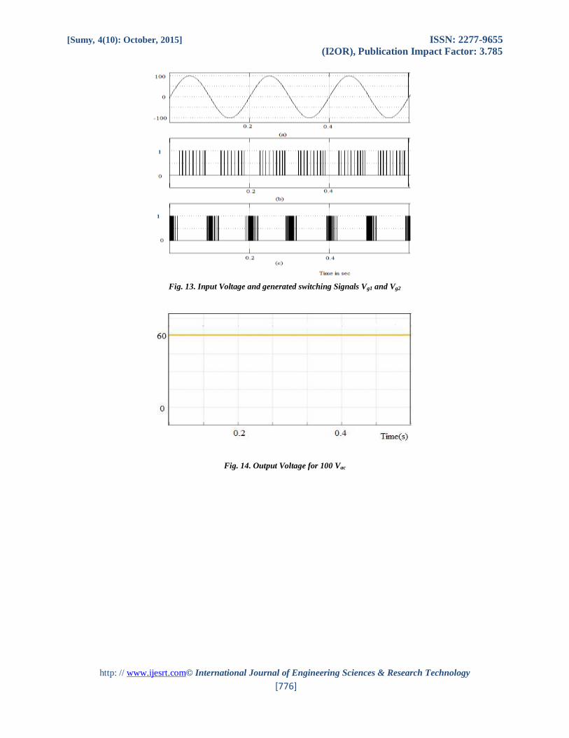
Fig. 13. Input Voltage and generated switching Signals Vg1 and Vg2
Fig. 14. Output Voltage for 100 Vac
[Sumy, 4(10): October, 2015] ISSN: 2277-9655
(I2OR), Publication Impact Factor: 3.785
http: // www.ijesrt.com© International Journal of Engineering Sciences & Research Technology
[777]
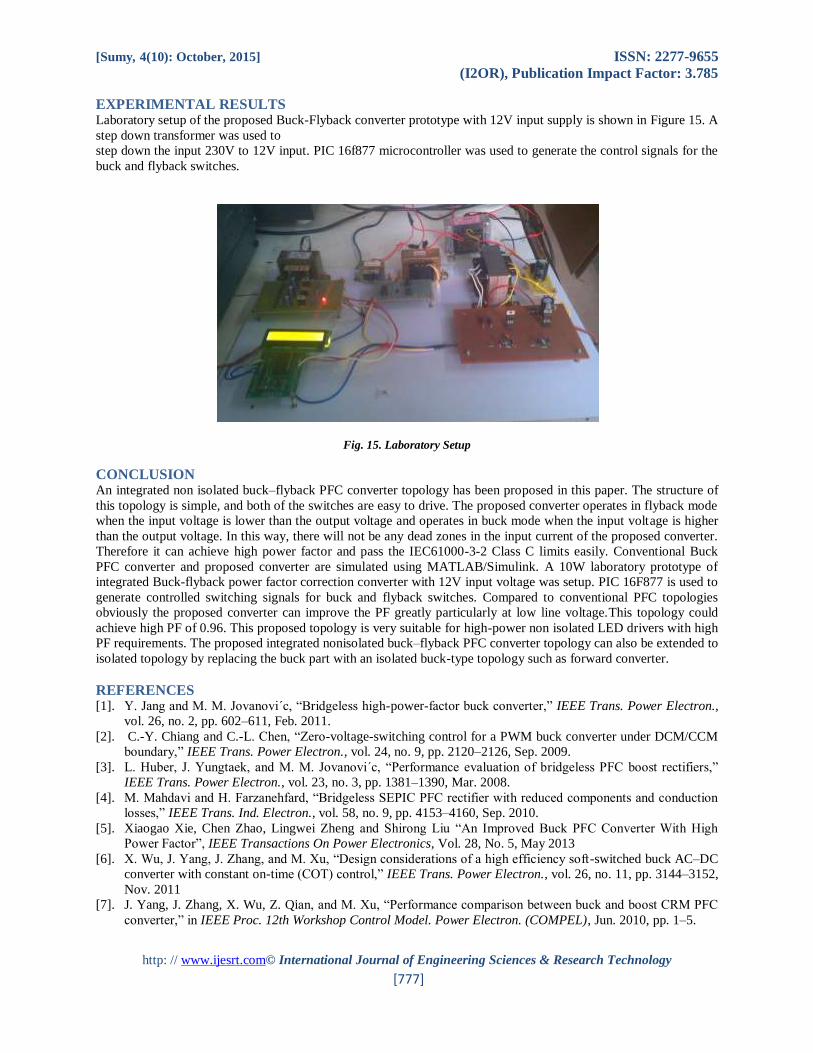
EXPERIMENTAL RESULTS Laboratory setup of the proposed Buck-Flyback converter prototype with 12V input supply is shown in Figure 15. A
step down transformer was used to
step down the input 230V to 12V input. PIC 16f877 microcontroller was used to generate the control signals for the
buck and flyback switches.
Fig. 15. Laboratory Setup
CONCLUSION An integrated non isolated buck–flyback PFC converter topology has been proposed in this paper. The structure of
this topology is simple, and both of the switches are easy to drive. The proposed converter operates in flyback mode
when the input voltage is lower than the output voltage and operates in buck mode when the input voltage is higher
than the output voltage. In this way, there will not be any dead zones in the input current of the proposed converter.
Therefore it can achieve high power factor and pass the IEC61000-3-2 Class C limits easily. Conventional Buck
PFC converter and proposed converter are simulated using MATLAB/Simulink. A 10W laboratory prototype of
integrated Buck-flyback power factor correction converter with 12V input voltage was setup. PIC 16F877 is used to
generate controlled switching signals for buck and flyback switches. Compared to conventional PFC topologies
obviously the proposed converter can improve the PF greatly particularly at low line voltage.This topology could
achieve high PF of 0.96. This proposed topology is very suitable for high-power non isolated LED drivers with high
PF requirements. The proposed integrated nonisolated buck–flyback PFC converter topology can also be extended to
isolated topology by replacing the buck part with an isolated buck-type topology such as forward converter.
REFERENCES [1]. Y. Jang and M. M. Jovanovi´c, “Bridgeless high-power-factor buck converter,” IEEE Trans. Power Electron.,
vol. 26, no. 2, pp. 602–611, Feb. 2011.
[2]. C.-Y. Chiang and C.-L. Chen, “Zero-voltage-switching control for a PWM buck converter under DCM/CCM
boundary,” IEEE Trans. Power Electron., vol. 24, no. 9, pp. 2120–2126, Sep. 2009.
[3]. L. Huber, J. Yungtaek, and M. M. Jovanovi´c, “Performance evaluation of bridgeless PFC boost rectifiers,”
IEEE Trans. Power Electron., vol. 23, no. 3, pp. 1381–1390, Mar. 2008.
[4]. M. Mahdavi and H. Farzanehfard, “Bridgeless SEPIC PFC rectifier with reduced components and conduction
losses,” IEEE Trans. Ind. Electron., vol. 58, no. 9, pp. 4153–4160, Sep. 2010.
[5]. Xiaogao Xie, Chen Zhao, Lingwei Zheng and Shirong Liu “An Improved Buck PFC Converter With High
Power Factor”, IEEE Transactions On Power Electronics, Vol. 28, No. 5, May 2013
[6]. X. Wu, J. Yang, J. Zhang, and M. Xu, “Design considerations of a high efficiency soft-switched buck AC–DC
converter with constant on-time (COT) control,” IEEE Trans. Power Electron., vol. 26, no. 11, pp. 3144–3152,
Nov. 2011
[7]. J. Yang, J. Zhang, X. Wu, Z. Qian, and M. Xu, “Performance comparison between buck and boost CRM PFC
converter,” in IEEE Proc. 12th Workshop Control Model. Power Electron. (COMPEL), Jun. 2010, pp. 1–5.

[Sumy, 4(10): October, 2015] ISSN: 2277-9655
(I2OR), Publication Impact Factor: 3.785
http: // www.ijesrt.com© International Journal of Engineering Sciences & Research Technology
[778]
[8]. M. A. Al-Saffar, E. H. Ismail, and A. J. Sabzali, “Integrated buck–boost quadratic buck PFC rectifier for
universal input applications,” IEEE Trans. Power Electron., vol. 24, no. 12, pp. 2886–2896, Dec. 2009.
[9]. J. Marcos Alonso, J. Viña, D. Gacio, L. Campa, G. Martínez, and R. Osorio, “Analysis and design of the
quadratic buck–boost converter as a high-power-factor driver for power-LED Lamps,” in Proc. IEEE IECON,
Glendale, AZ, 2010, pp. 2541–2546
[10]. J. M. Alonso, M. A. D. Costa, and C. Ordiz, “Integrated buck–flyback converter as a high-power-factor off-
line power supply,” IEEE Trans. Ind. Electron., vol. 55, no. 3, pp. 1090–1100, Mar. 2008.
[11]. M. A. Dalla Costa, J. M. Alonso, J. C. Miranda, J. Garcia, and D. G. Lamar, “A single-stage high-power-factor
electronic ballast based on integrated buck flyback converter to supply metal halide lamps,” IEEE Trans. Ind.
Electron., vol. 55, no. 3, pp. 1112–1122, Mar. 2008
[12]. Gacio, J. M. Alonso, A. J. Calleja, J. García, and M. Rico-Secades, “Universal-input single-stage high-power-
factor power supply for HBLEDs based on integrated buck–flyback converter,” IEEE Trans. Ind. Electron.,
vol. 58, no. 2, pp. 589–599, Feb. 2011.
[13]. G. Spiazzi and S. Buso, “Power factor preregulators based on combined buck–flyback topologies,” IEEE
Trans. Power Electron., vol. 15, no. 2, pp. 197–204, Mar. 2000.
AUTHOR BIBLIOGRAPHY
Sumy P S
Received B. Tech degree in Electrical and
Electronics Engineering from Government
Engineering College, Idukki, Kerala, India.
and M.Tech in power Electronics from NSS
College of Engineering Palakkad, Kerala,
India