Embed Size (px)
Citation preview
Overview
2
What is an INMAPS device?
The Cherwell chip
Characterisation work
Test beam
Applications
Chip design for ALICE
Outlook
What is an INMAPS device?
3
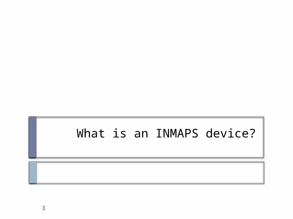
INMAPS:
4
Charge collection inefficiency across a pixel is detrimental to efficient system design: Want to have smart pixels Requires circuitry in pixel for rudimentary signal
processing Use a deep p-well to shield the N-well in chip electronics
Isolated N-well Monolithic Active Pixel Sensors
STANDARD CMOS INMAPSe.g. See J.P. Crooks et al., Proc. IEEE Symp on Nucl. Sci (2007), 2, 931-935. M. Stanitzki et al., Proc. IEEE Symp. on Nucl. Sci. (2007), 1, 254-258 J. A. Ballin et al. Pixels ,Sensors 2008, 8(9), 5336-5351.
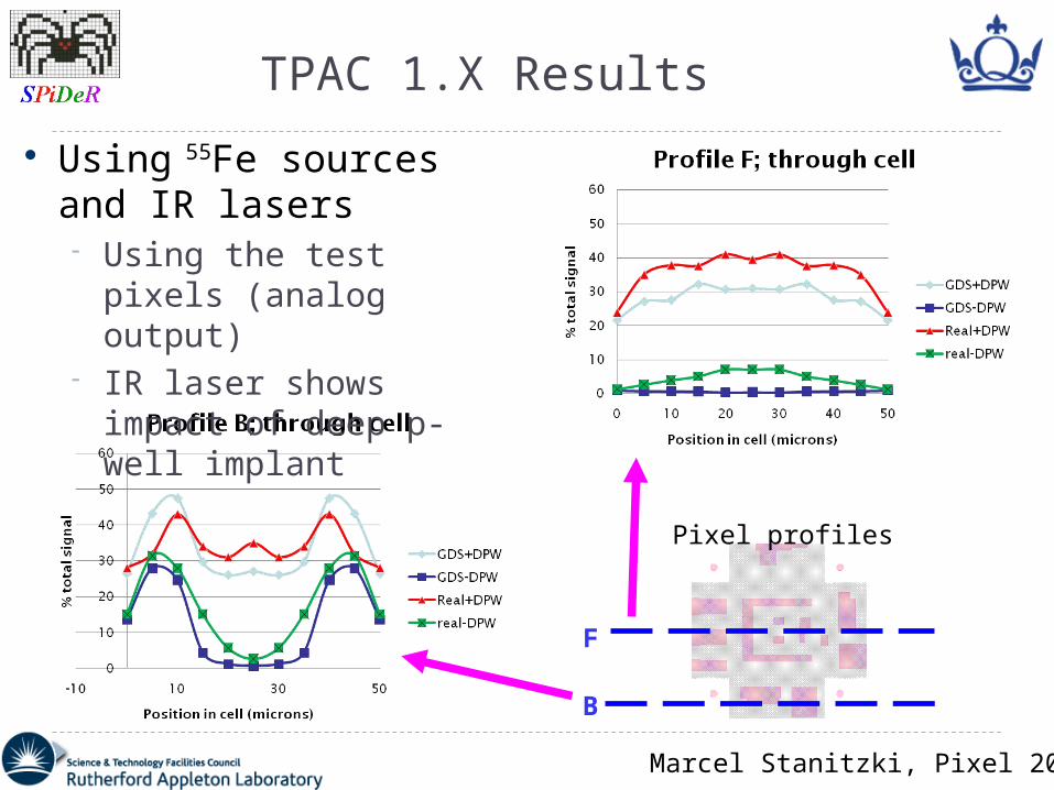
TPAC 1.X Results
F
B
Pixel profiles
Using 55Fe sources and IR lasers Using the test pixels (analog
output) IR laser shows impact of
deep p-well implant
Marcel Stanitzki, Pixel 2010
)
Typical resistivity ~ 10-
100Ωcm
High resistivity
~ 1-10kΩcm
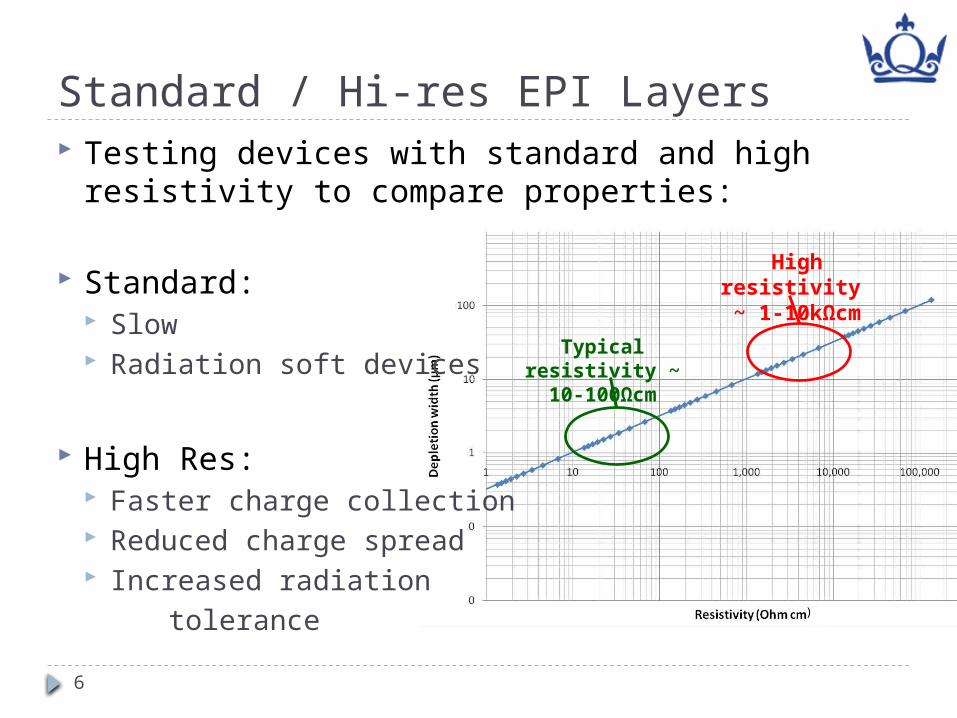
Standard / Hi-res EPI Layers
6
Testing devices with standard and high resistivity to compare properties:
Standard: Slow Radiation soft devices
High Res: Faster charge collection Reduced charge spread Increased radiation tolerance
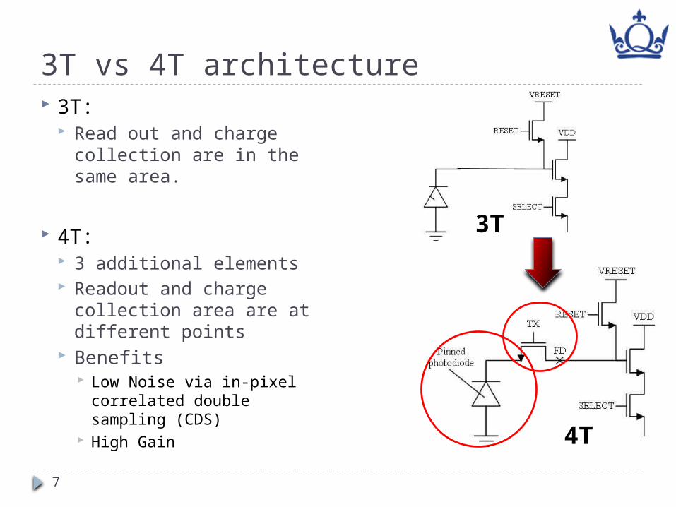
3T vs 4T architecture
7
3T: Read out and charge collection
are in the same area.
4T: 3 additional elements Readout and charge collection
area are at different points Benefits
Low Noise via in-pixel correlated double sampling (CDS)
High Gain
3T
4T
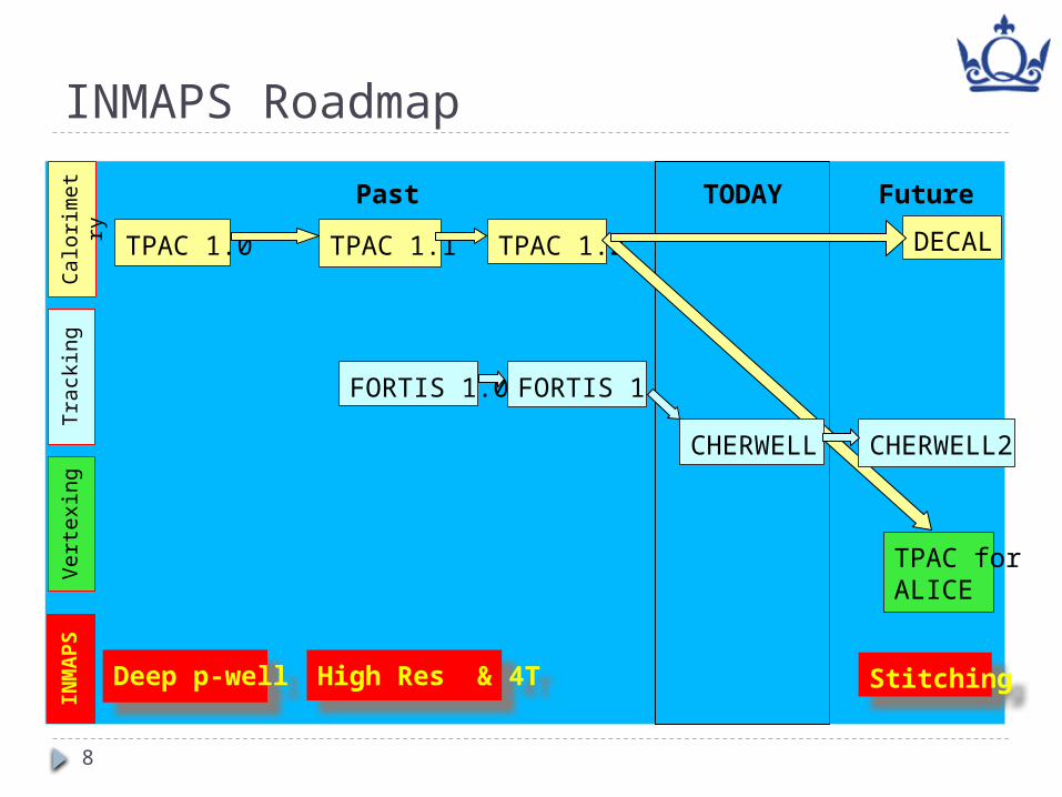
INMAPS Roadmap
8
Calo
rim
etr
yTr
ack
ing
Vert
exin
g
Deep p-well
TPAC 1.0 TPAC 1.2TPAC 1.1
High Res & 4T
INM
AP
S
FORTIS 1.0 FORTIS 1.1
TODAY
Stitching
TPAC forALICE
CHERWELL CHERWELL2
FuturePast
DECAL
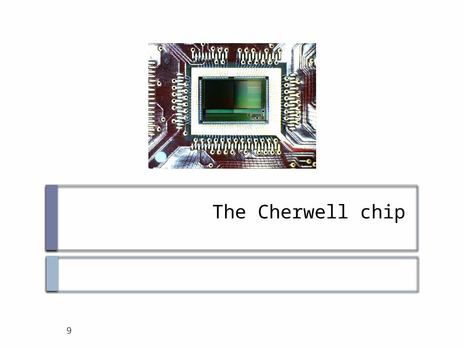
The Cherwell chip
9
The Cherwell Chip
10
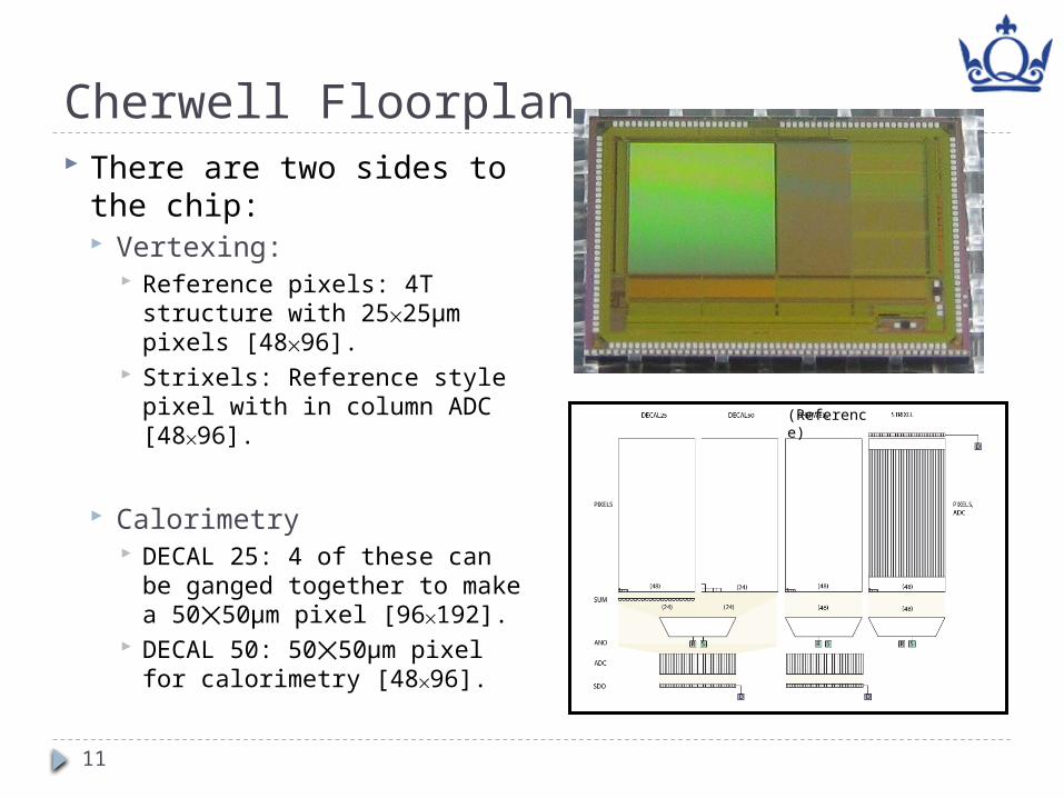
Cherwell Floorplan
11
There are two sides to the chip: Vertexing:
Reference pixels: 4T structure with 25✕25 m μpixels [48✕96].
Strixels: Reference style pixel with in column ADC [48✕96].
Calorimetry DECAL 25: 4 of these can be
ganged together to make a 50✕50 m pixel [96μ ✕192].
DECAL 50: 50✕50 m pixel μfor calorimetry [48✕96].
(Reference)
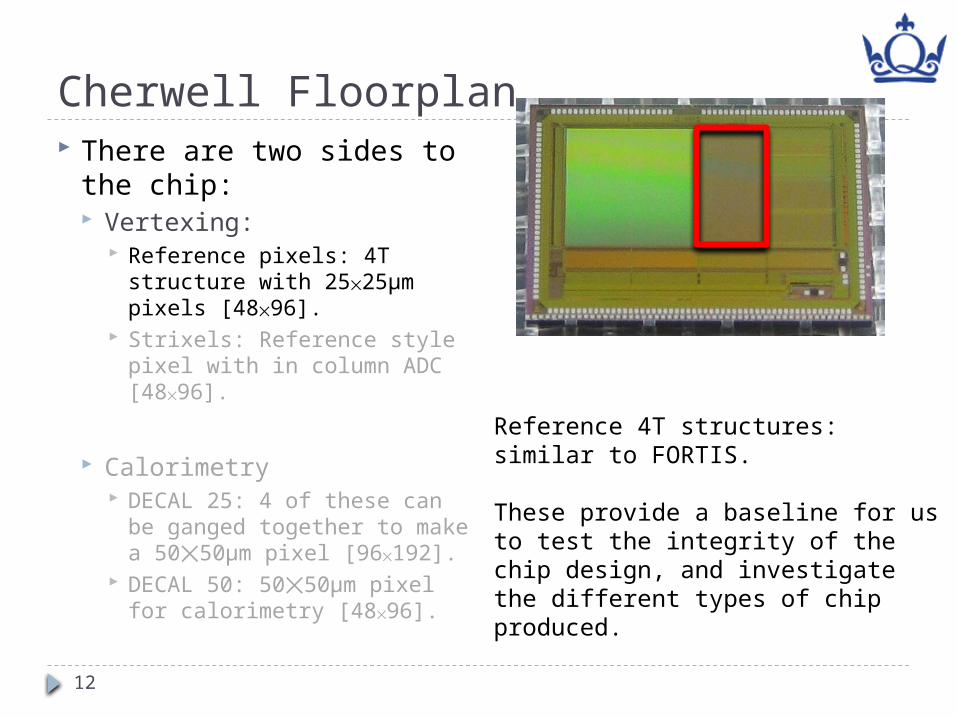
Cherwell Floorplan
12
There are two sides to the chip: Vertexing:
Reference pixels: 4T structure with 25✕25 m μpixels [48✕96].
Strixels: Reference style pixel with in column ADC [48✕96].
Calorimetry DECAL 25: 4 of these can be
ganged together to make a 50✕50 m pixel [96μ ✕192].
DECAL 50: 50✕50 m pixel μfor calorimetry [48✕96].
Reference 4T structures: similar to FORTIS.
These provide a baseline for us to test the integrity of the chip design, and investigate the different types of chip produced.
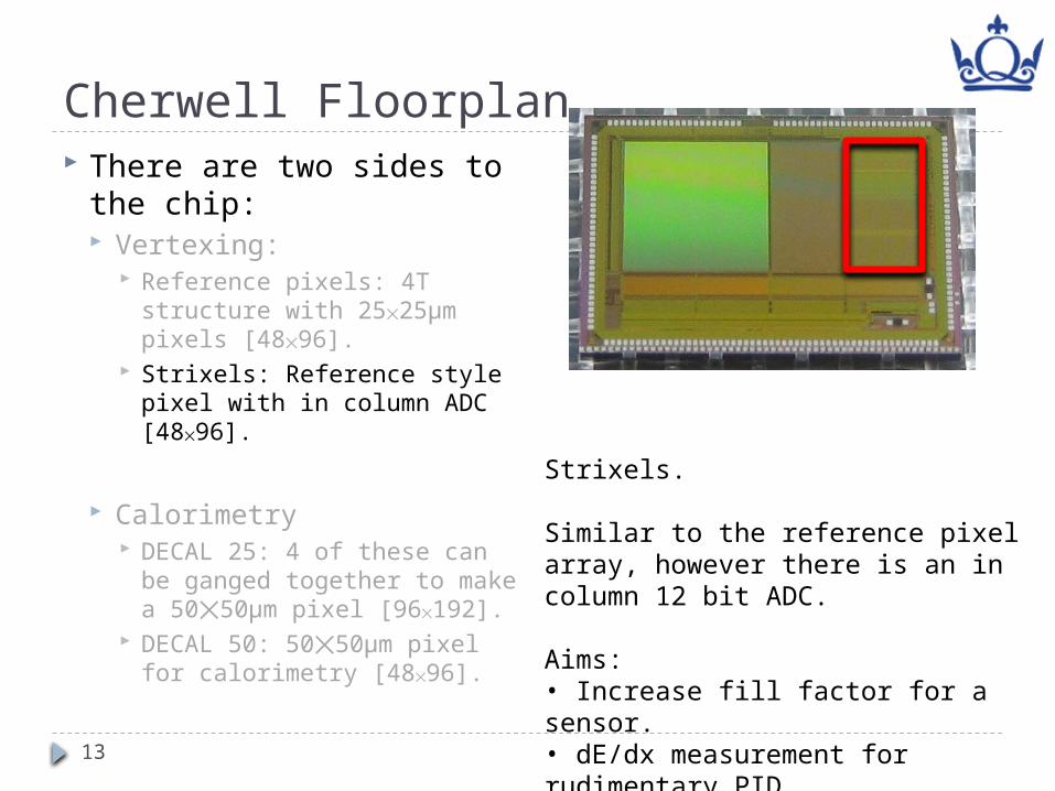
Cherwell Floorplan
13
There are two sides to the chip: Vertexing:
Reference pixels: 4T structure with 25✕25 m μpixels [48✕96].
Strixels: Reference style pixel with in column ADC [48✕96].
Calorimetry DECAL 25: 4 of these can be
ganged together to make a 50✕50 m pixel [96μ ✕192].
DECAL 50: 50✕50 m pixel μfor calorimetry [48✕96].
Strixels.
Similar to the reference pixel array, however there is an in column 12 bit ADC.
Aims:• Increase fill factor for a sensor.• dE/dx measurement for rudimentary PID.• Reduce need for ancillary electronics.

Cherwell Floorplan
14
There are two sides to the chip: Vertexing:
Reference pixels: 4T structure with 25✕25 m μpixels [48✕96].
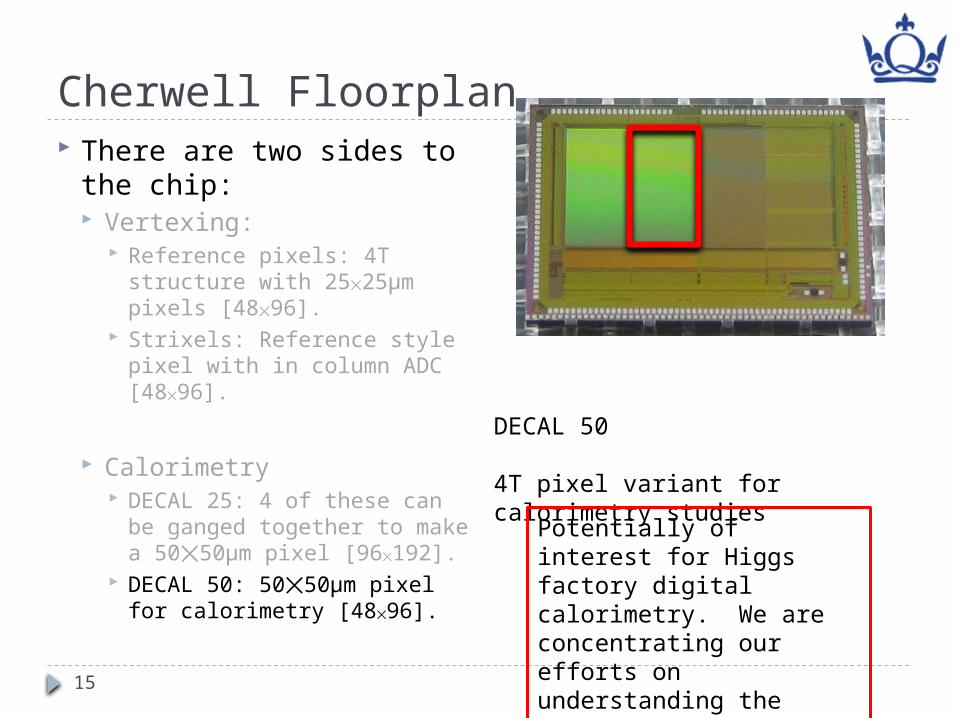
Strixels: Reference style pixel with in column ADC [48✕96].
Calorimetry DECAL 25: 4 of these can be
ganged together to make a 50✕50 m pixel [96μ ✕192].
DECAL 50: 50✕50 m pixel μfor calorimetry [48✕96].
DECAL 25
4T pixel variant for calorimetry studies
Potentially of interest for Higgs factory digital calorimetry. We are concentrating our efforts on understanding the reference and strixel part of the chip first.
Cherwell Floorplan
15
There are two sides to the chip: Vertexing:
Reference pixels: 4T structure with 25✕25 m μpixels [48✕96].
Strixels: Reference style pixel with in column ADC [48✕96].
Calorimetry DECAL 25: 4 of these can be
ganged together to make a 50✕50 m pixel [96μ ✕192].
DECAL 50: 50✕50 m pixel μfor calorimetry [48✕96].
DECAL 50
4T pixel variant for calorimetry studies
Potentially of interest for Higgs factory digital calorimetry. We are concentrating our efforts on understanding the reference and strixel part of the chip first.
Maximising the fill factor
16
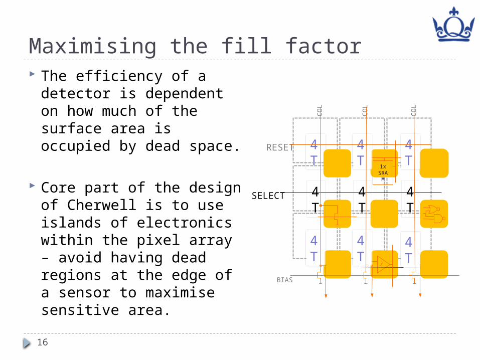
The efficiency of a detector is dependent on how much of the surface area is occupied by dead space.
Core part of the design of Cherwell is to use islands of electronics within the pixel array – avoid having dead regions at the edge of a sensor to maximise sensitive area.
4T
SELECT
CO
L
RESET
CO
L
CO
L
1xSRAM
BIAS
CO
L
CO
L
CO
L
4T
4T
4T
4T
4T
4T
4T
4T
The Cherwell Chip
17
This seminar will mostly
concentrate on tests of the
reference pixel part of
Cherwell.
Characterisation work
Results on the reference and strixel parts of Cherwell
18
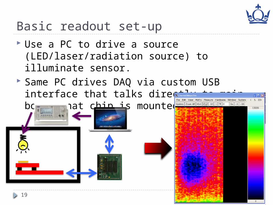
Basic readout set-up
19
Use a PC to drive a source (LED/laser/radiation source) to illuminate sensor.
Same PC drives DAQ via custom USB interface that talks directly to main board that chip is mounted on.
Characterisation work
20
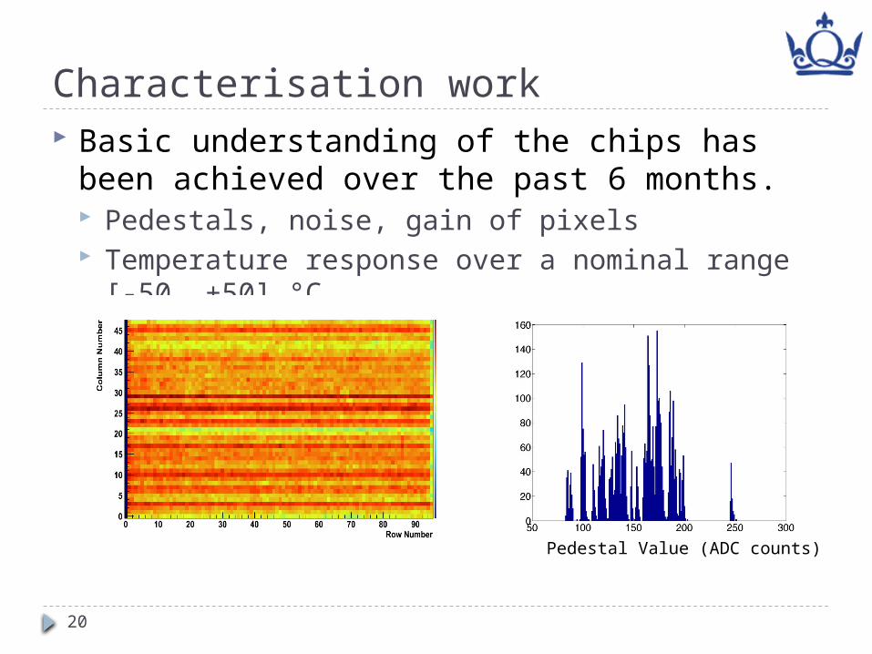
Basic understanding of the chips has been achieved over the past 6 months. Pedestals, noise, gain of pixels Temperature response over a nominal range [-50, +50] °C
Pedestal Value (ADC counts)
Photon Transfer Curve results (PTC)
21
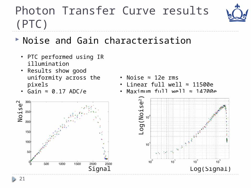
Noise and Gain characterisation
• PTC performed using IR illumination
• Results show good uniformity across the pixels
• Gain ≈ 0.17 ADC/e
• Noise ≈ 12e rms• Linear full well ≈ 11500e• Maximum full well ≈ 14700e
Log(Signal)
Log
(Nois
e2)
Signal
Nois
e2
Characterisation work
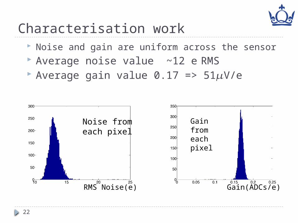
22
Noise and gain are uniform across the sensor Average noise value ~12 e RMS Average gain value 0.17 => 51 V/e𝜇
Noise from each pixel
RMS Noise(e)
Gain from each pixel
Gain(ADCs/e)
Source tests
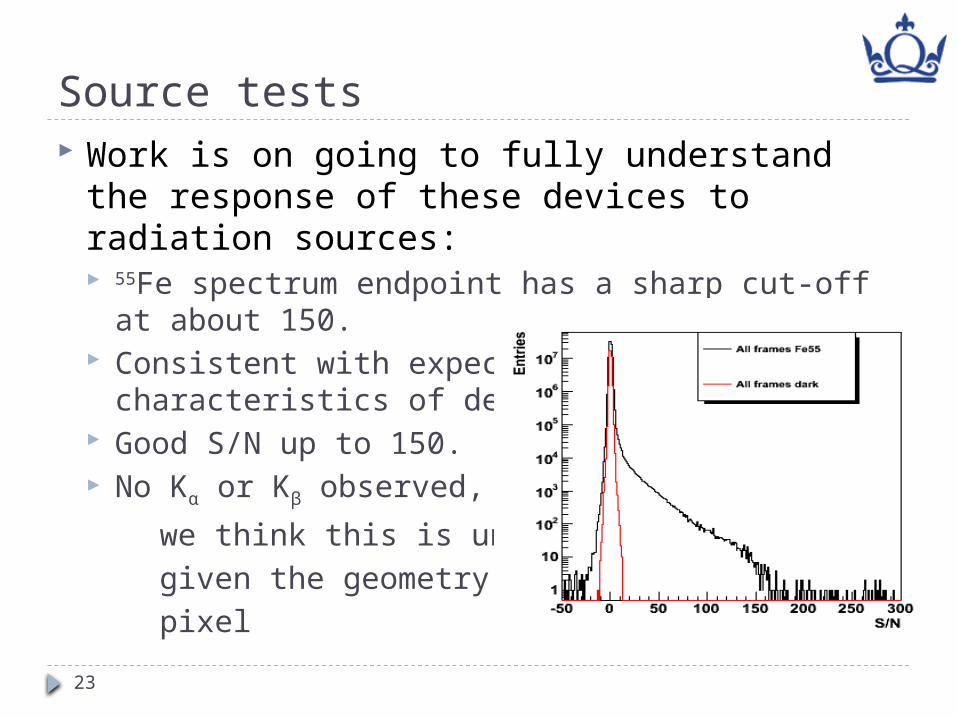
23
Work is on going to fully understand the response of these devices to radiation sources: 55Fe spectrum endpoint has a sharp cut-off at about 150. Consistent with expectations from the PTC characteristics of
devices. Good S/N up to 150. No Kα or Kβ observed,
we think this is understood given the geometry of the pixel
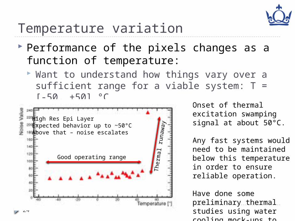
Temperature variation
24
Performance of the pixels changes as a function of temperature: Want to understand how things vary over a sufficient range
for a viable system: T = [-50, +50] °C.
Onset of thermal excitation swamping signal at about 50°C.
Any fast systems would need to be maintained below this temperature in order to ensure reliable operation.
Have done some preliminary thermal studies using water cooling mock-ups to explore system integration.
High Res Epi LayerExpected behavior up to ~50°CAbove that – noise escalates
Good operating rangeTherm
al ru
naw
ay
Test beam
25
26
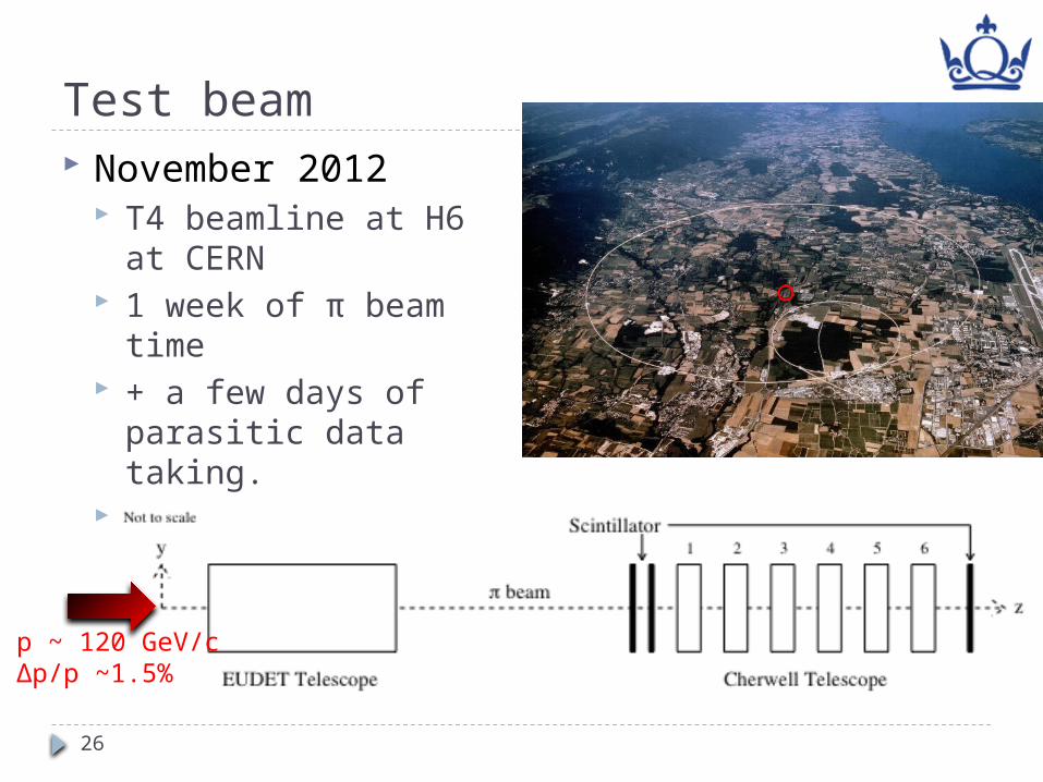
Test beam November 2012
T4 beamline at H6 at CERN 1 week of beam timeπ + a few days of parasitic
data taking. Aim: understand
resolution, charge sharing, and efficiency of Cherwell.
p ~ 120 GeV/cΔp/p ~1.5%
Test beam
27
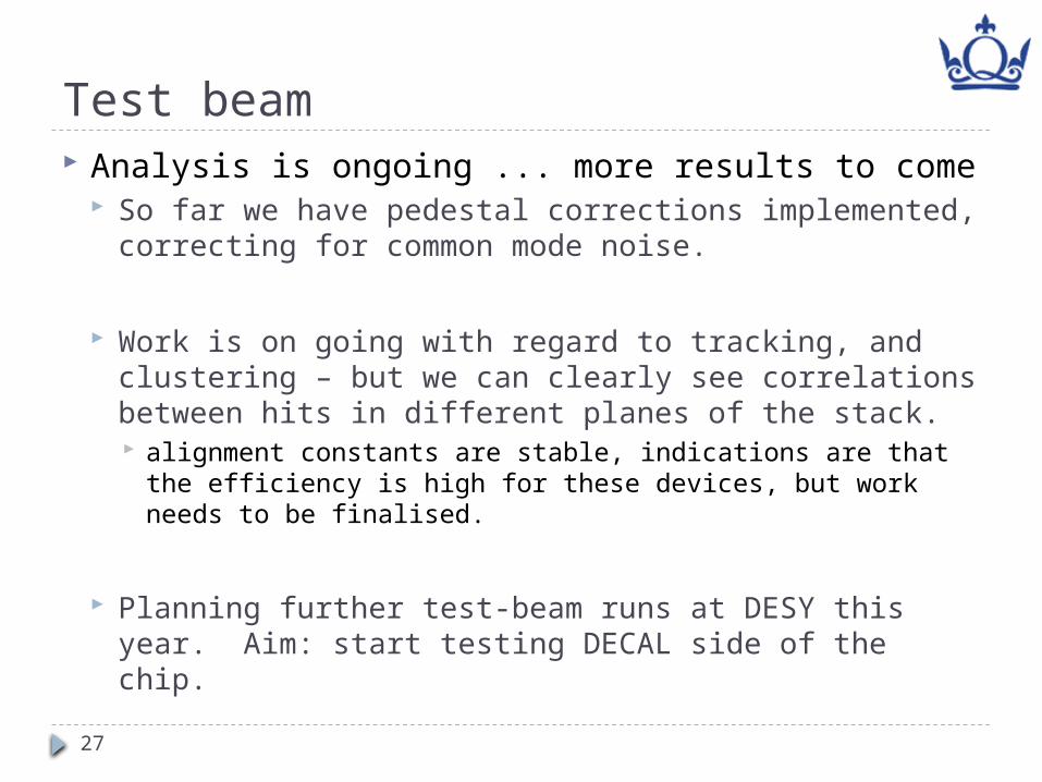
Analysis is ongoing ... more results to come So far we have pedestal corrections implemented,
correcting for common mode noise.
Work is on going with regard to tracking, and clustering – but we can clearly see correlations between hits in different planes of the stack. alignment constants are stable, indications are that the efficiency
is high for these devices, but work needs to be finalised.
Planning further test-beam runs at DESY this year. Aim: start testing DECAL side of the chip.
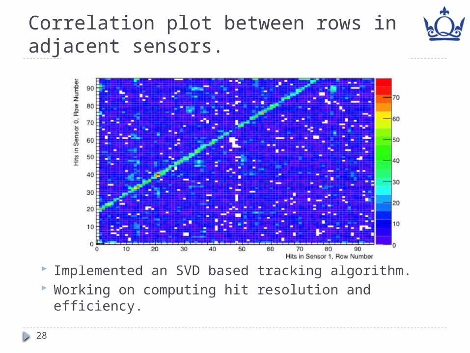
Correlation plot between rows in adjacent sensors.
28
Implemented an SVD based tracking algorithm. Working on computing hit resolution and efficiency.
Applications
A few potential uses for this technology (there are many)
29
30
Vertexing: Fast, precision, low mass detection of charged particles in the
vicinity of the interaction region of a detector. Can be used with one or more layers. X0 is dominated by two things:
Thickness of silicon: can back-thin sensors to ~20 m giving a very μlow mass system
Speed of readout: fast readout requires active cooling and adds mass Projects pursuing this technology:
SuperB: Particle physics experiment at the Cabibbo Lab in Italy. Searching for new physics at the intensity frontier.
ALICE: Nuclear Physics experiment at the LHC. Searching for a deeper understanding of matter at the energy frontier.
e.g. See Bevan et al., NIMA 643 (2011), pp. 29-35
31
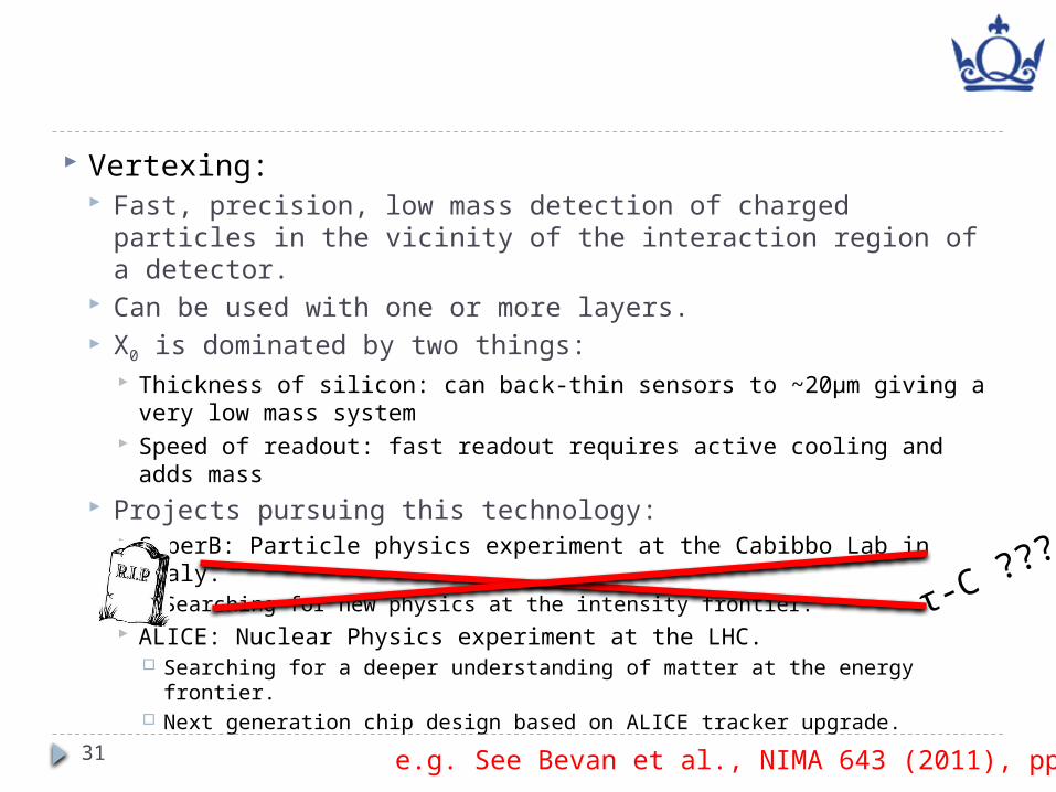
Vertexing: Fast, precision, low mass detection of charged particles in the
vicinity of the interaction region of a detector. Can be used with one or more layers. X0 is dominated by two things:
Thickness of silicon: can back-thin sensors to ~20 m giving a very μlow mass system
Speed of readout: fast readout requires active cooling and adds mass Projects pursuing this technology:
SuperB: Particle physics experiment at the Cabibbo Lab in Italy. Searching for new physics at the intensity frontier.
ALICE: Nuclear Physics experiment at the LHC. Searching for a deeper understanding of matter at the energy frontier. Next generation chip design based on ALICE tracker upgrade.
e.g. See Bevan et al., NIMA 643 (2011), pp. 29-35
τ-C ???
32
Calorimetry High granularity large area detector for particle flow
reconstruction and identification algorithms: Use the shower shape to distinguish between particle species
based on how they interact in the calorimeter e.g. pixel-W sandwich based calorimeter concept: CALICE (Higgs
Factory/CLIC) Variant of a standard CMOS process makes this technology cheap
enough to be of interest for such applications.
e.g. See J A Ballin et al 2011 JINST 6 P05009
33
Other uses Characterisation of these devices over a range of
temperatures is driven by a desire to understand: the maximum operating temperature of a functional device. how devices work over a "normal" range of actively cooled
temperatures. how they work in a regime of interest for ground based astronomy
(here you want to cool sufficiently to be able to eliminate IR background from your detector: need to operate at LN2 temperatures).
Also of interest to T2K Re: LAr calorimetry. how low can you go?
These issues are all related to building a "system".
Work in progress
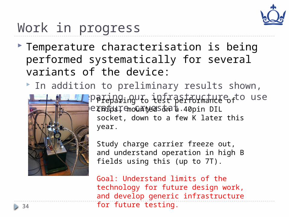
34
Temperature characterisation is being performed systematically for several variants of the device: In addition to preliminary results shown, we are preparing
our infrastructure to use a low temperature cryostat.
Preparing to test performance of chips, mounted on a 40pin DIL socket, down to a few K later this year.
Study charge carrier freeze out, and understand operation in high B fields using this (up to 7T).
Goal: Understand limits of the technology for future design work, and develop generic infrastructure for future testing.
CMOS Image Sensor for the ALICE ITS
Work in progress
35
Basic concept.
36
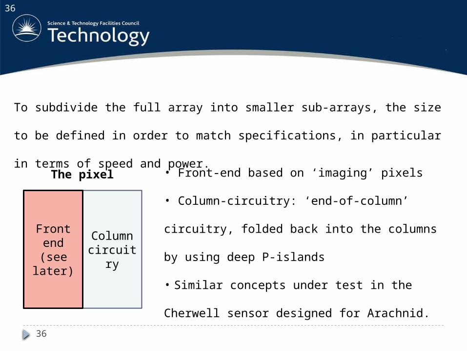
To subdivide the full array into smaller sub-arrays, the size to be defined
in order to match specifications, in particular in terms of speed and
power.
Column circuitry
Front end (see later)
The pixel • Front-end based on ‘imaging’ pixels
• Column-circuitry: ‘end-of-column’ circuitry,
folded back into the columns by using deep P-
islands
• Similar concepts under test in the Cherwell
sensor designed for Arachnid.
36
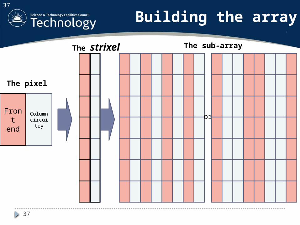
37
Building the array
37
Column circuitr
y
Front end
The pixel
The strixel The sub-array
or
38
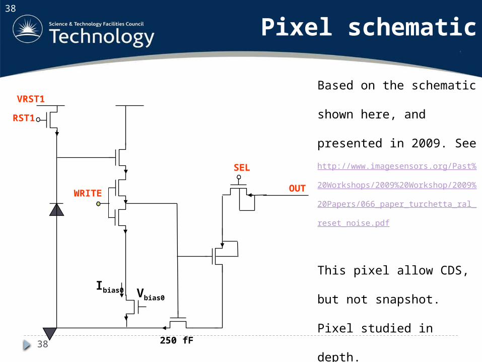
Pixel schematic
SEL
RST1
VRST1
Ibias0 Vbias0
OUTWRITE
250 fF38
Based on the schematic
shown here, and
presented in 2009. See
http://www.imagesensors.org/Past%20W
orkshops/2009%20Workshop/2009%20P
apers/066_paper_turchetta_ral_reset_no
ise.pdf
This pixel allow CDS, but
not snapshot.
Pixel studied in depth.
39
Timing
SELRST
VRST
OUTWRITE
SEL
WRITE
RST
Integration Sample Reset
Sample
Signal
Reset pixel
40
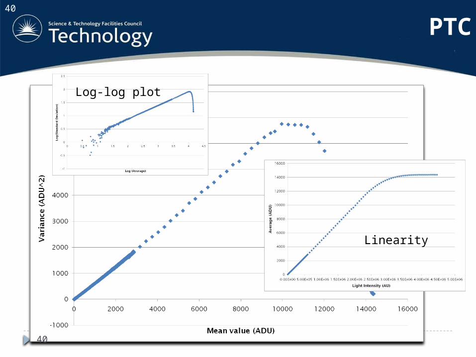
PTC
40
Log-log plot
Linearity
41
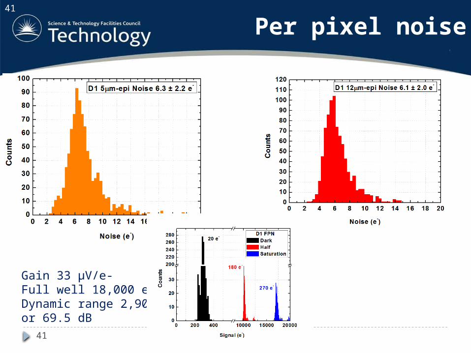
Per pixel noise
41
Gain 33 µV/e-Full well 18,000 e-Dynamic range 2,900or 69.5 dB
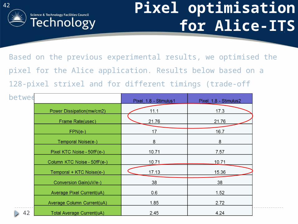
42 Pixel optimisation for Alice-ITS
42
Based on the previous experimental results, we optimised the pixel for
the Alice application. Results below based on a 128-pixel strixel and for
different timings (trade-off between noise and power)
43
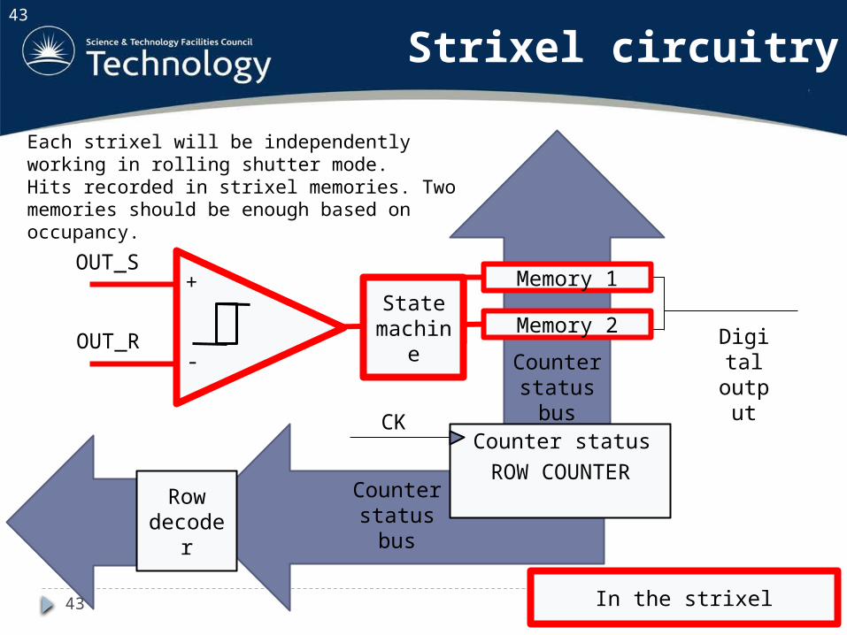
Strixel circuitry
43
+
-
OUT_S
OUT_R
ROW COUNTER
CK
Memory 1
Memory 2
Counter status
Counter status
bus
State machin
eDigita
l outpu
t
Counter status
bus
Row decode
r
In the strixel
Each strixel will be independently working in rolling shutter mode.Hits recorded in strixel memories. Two memories should be enough based on occupancy.
44
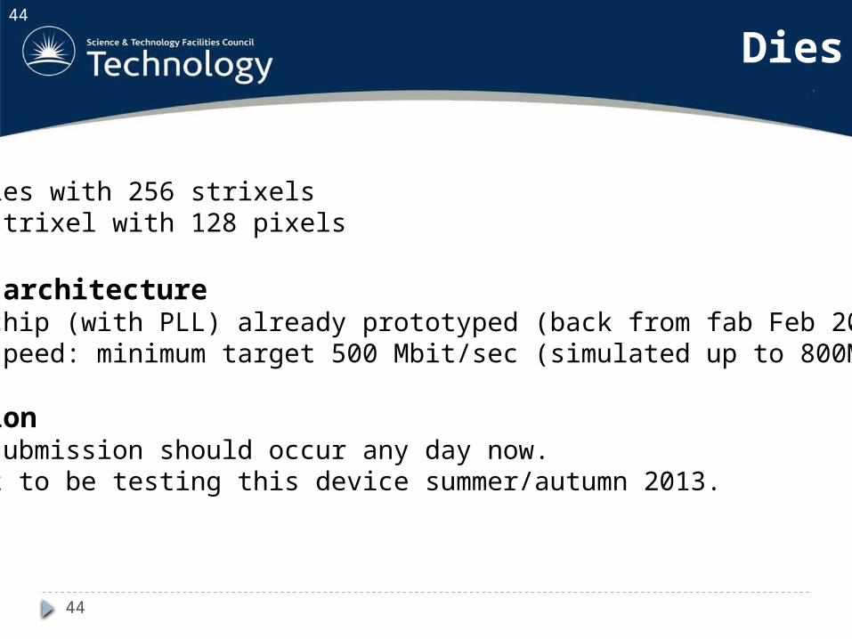
Dies
44
SensorsTwo dies with 256 strixelsEach strixel with 128 pixels
Readout architectureLVDS chip (with PLL) already prototyped (back from fab Feb 2013)LVDS speed: minimum target 500 Mbit/sec (simulated up to 800Mbit/sec)
SubmissionChip submission should occur any day now.Expect to be testing this device summer/autumn 2013.

Outlook
45
46
Cherwell is functioning well Bench-test characterisation yielded interesting initial results so far.
First results from test beam are promising Reference/Strixel parts of the chip
Basic operational requirements are understood plan to continue exploring these aspects.
DECAL needs more investigation planning a test beam at DESY to study this half of the chip.
One step closer to being able to build a fully integrated INMAPS based detector system.
To Do
47
Test beam analysis is ongoing: Aim to get efficiency and a better understanding of clustering. Requires tracking software refinement.
Bench-top characterisation: Laser hit maps to study uniformity of response across pixels.
Radiation hardness The pinned photodiode is suspected to be radiation soft, want to investigate
this device in more detail. Further our understanding of the operational envelope:
crucial if we want to be able to map out a wider range of possible applications for devices based on this technology.
Continuing to develop infrastructure to this end. Chip design:
Expect a new chip submission this week for a next generation device for vertexing (ALICE Tracker prototype).
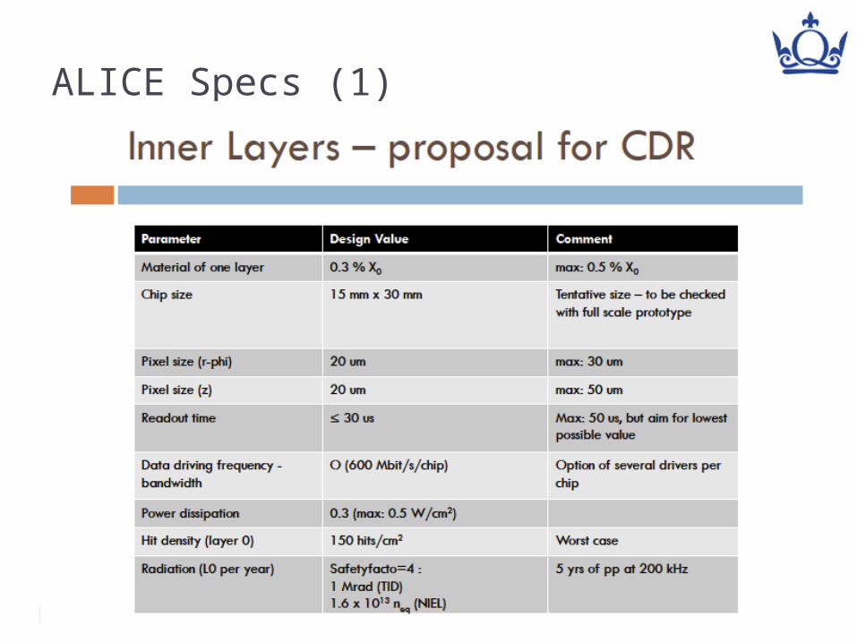
ALICE Specs (1)
48
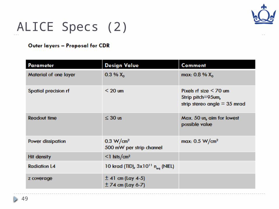
ALICE Specs (2)
49