Embed Size (px)
Citation preview

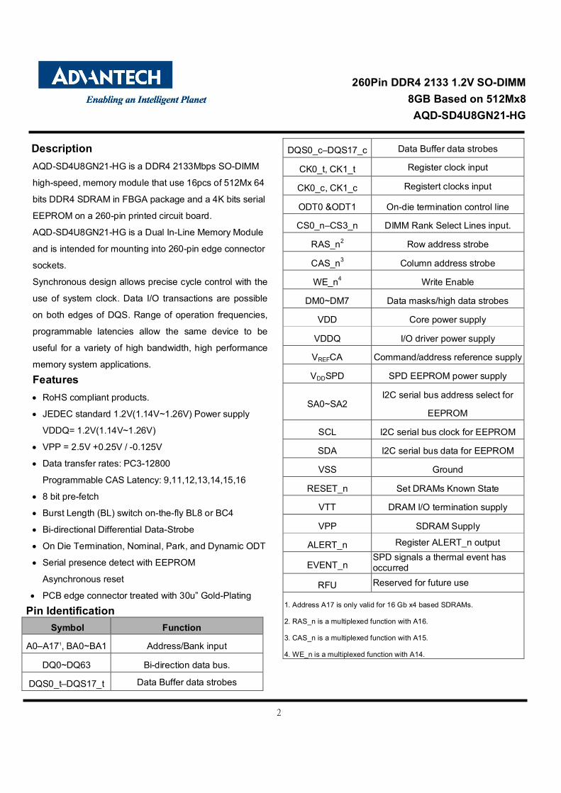
260Pin DDR4 2133 1.2V SO-DIMM 8GB Based on 512Mx8 AQD-SD4U8GN21-HG
1
Advantech
AQD-SD4U8GN21-HG Datasheet
Rev. 0.0 2015-12-09
260Pin DDR4 2133 1.2V SO-DIMM 8GB Based on 512Mx8 AQD-SD4U8GN21-HG
2
Description AQD-SD4U8GN21-HG is a DDR4 2133Mbps SO-DIMM
high-speed, memory module that use 16pcs of 512Mx 64
bits DDR4 SDRAM in FBGA package and a 4K bits serial
EEPROM on a 260-pin printed circuit board.
AQD-SD4U8GN21-HG is a Dual In-Line Memory Module
and is intended for mounting into 260-pin edge connector
sockets.
Synchronous design allows precise cycle control with the
use of system clock. Data I/O transactions are possible
on both edges of DQS. Range of operation frequencies,
programmable latencies allow the same device to be
useful for a variety of high bandwidth, high performance
memory system applications. Features
RoHS compliant products.
JEDEC standard 1.2V(1.14V~1.26V) Power supply
VDDQ= 1.2V(1.14V~1.26V)
VPP = 2.5V +0.25V / -0.125V
Data transfer rates: PC3-12800
Programmable CAS Latency: 9,11,12,13,14,15,16
8 bit pre-fetch
Burst Length (BL) switch on-the-fly BL8 or BC4
Bi-directional Differential Data-Strobe
On Die Termination, Nominal, Park, and Dynamic ODT
Serial presence detect with EEPROM
Asynchronous reset
PCB edge connector treated with 30u” Gold-Plating
Pin Identification
Symbol Function
A0–A171, BA0~BA1 Address/Bank input
DQ0~DQ63 Bi-direction data bus.
DQS0_t–DQS17_t Data Buffer data strobes
DQS0_c–DQS17_c Data Buffer data strobes
CK0_t, CK1_t Register clock input
CK0_c, CK1_c Registert clocks input
ODT0 &ODT1 On-die termination control line
CS0_n–CS3_n DIMM Rank Select Lines input.
RAS_n2 Row address strobe
CAS_n3 Column address strobe
WE_n4 Write Enable
DM0~DM7 Data masks/high data strobes
VDD Core power supply
VDDQ I/O driver power supply
VREFCA Command/address reference supply
VDDSPD SPD EEPROM power supply
SA0~SA2 I2C serial bus address select for
EEPROM
SCL I2C serial bus clock for EEPROM
SDA I2C serial bus data for EEPROM
VSS Ground
RESET_n Set DRAMs Known State
VTT DRAM I/O termination supply
VPP SDRAM Supply
ALERT_n Register ALERT_n output
EVENT_n SPD signals a thermal event has occurred
RFU Reserved for future use
1. Address A17 is only valid for 16 Gb x4 based SDRAMs.
2. RAS_n is a multiplexed function with A16.
3. CAS_n is a multiplexed function with A15.
4. WE_n is a multiplexed function with A14.

260Pin DDR4 2133 1.2V SO-DIMM 8GB Based on 512Mx8 AQD-SD4U8GN21-HG
3
Dimensions (Unit: millimeter)
Note:1. Tolerances on all dimensions +/-0.15mm unless otherwise specified.
260Pin DDR4 2133 1.2V SO-DIMM 8GB Based on 512Mx8 AQD-SD4U8GN21-HG
4
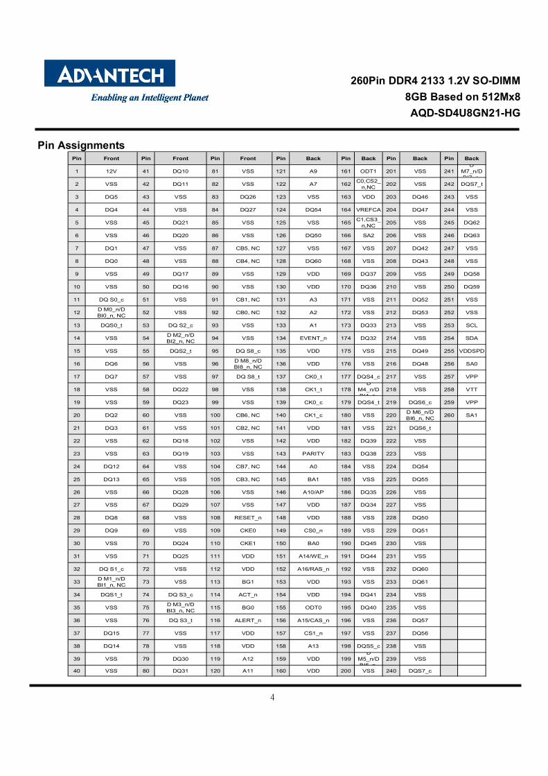
Pin Assignments Pin Front Pin Front Pin Front Pin Back Pin Back Pin Back Pin Back
1 12V 41 DQ10 81 VSS 121 A9 161 ODT1 201 VSS 241D
M7_n/DBI7_n,
2 VSS 42 DQ11 82 VSS 122 A7 162 C0,CS2_n,NC 202 VSS 242 DQS7_t
3 DQ5 43 VSS 83 DQ26 123 VSS 163 VDD 203 DQ46 243 VSS
4 DQ4 44 VSS 84 DQ27 124 DQ54 164 VREFCA 204 DQ47 244 VSS
5 VSS 45 DQ21 85 VSS 125 VSS 165 C1,CS3_n,NC 205 VSS 245 DQ62
6 VSS 46 DQ20 86 VSS 126 DQ50 166 SA2 206 VSS 246 DQ63
7 DQ1 47 VSS 87 CB5, NC 127 VSS 167 VSS 207 DQ42 247 VSS
8 DQ0 48 VSS 88 CB4, NC 128 DQ60 168 VSS 208 DQ43 248 VSS
9 VSS 49 DQ17 89 VSS 129 VDD 169 DQ37 209 VSS 249 DQ58
10 VSS 50 DQ16 90 VSS 130 VDD 170 DQ36 210 VSS 250 DQ59
11 DQ S0_c 51 VSS 91 CB1, NC 131 A3 171 VSS 211 DQ52 251 VSS
12 D M0_n/DBI0_n, NC 52 VSS 92 CB0, NC 132 A2 172 VSS 212 DQ53 252 VSS
13 DQS0_t 53 DQ S2_c 93 VSS 133 A1 173 DQ33 213 VSS 253 SCL
14 VSS 54 D M2_n/DBI2_n, NC 94 VSS 134 EVENT_n 174 DQ32 214 VSS 254 SDA
15 VSS 55 DQS2_t 95 DQ S8_c 135 VDD 175 VSS 215 DQ49 255 VDDSPD
16 DQ6 56 VSS 96 D M8_n/DBI8_n, NC 136 VDD 176 VSS 216 DQ48 256 SA0
17 DQ7 57 VSS 97 DQ S8_t 137 CK0_t 177 DQS4_c 217 VSS 257 VPP
18 VSS 58 DQ22 98 VSS 138 CK1_t 178D
M4_n/DBI4_n,
218 VSS 258 VTT
19 VSS 59 DQ23 99 VSS 139 CK0_c 179 DQS4_t 219 DQS6_c 259 VPP
20 DQ2 60 VSS 100 CB6, NC 140 CK1_c 180 VSS 220 D M6_n/DBI6_n, NC 260 SA1
21 DQ3 61 VSS 101 CB2, NC 141 VDD 181 VSS 221 DQS6_t
22 VSS 62 DQ18 102 VSS 142 VDD 182 DQ39 222 VSS
23 VSS 63 DQ19 103 VSS 143 PARITY 183 DQ38 223 VSS
24 DQ12 64 VSS 104 CB7, NC 144 A0 184 VSS 224 DQ54
25 DQ13 65 VSS 105 CB3, NC 145 BA1 185 VSS 225 DQ55
26 VSS 66 DQ28 106 VSS 146 A10/AP 186 DQ35 226 VSS
27 VSS 67 DQ29 107 VSS 147 VDD 187 DQ34 227 VSS
28 DQ8 68 VSS 108 RESET_n 148 VDD 188 VSS 228 DQ50
29 DQ9 69 VSS 109 CKE0 149 CS0_n 189 VSS 229 DQ51
30 VSS 70 DQ24 110 CKE1 150 BA0 190 DQ45 230 VSS
31 VSS 71 DQ25 111 VDD 151 A14/WE_n 191 DQ44 231 VSS
32 DQ S1_c 72 VSS 112 VDD 152 A16/RAS_n 192 VSS 232 DQ60
33 D M1_n/DBI1_n, NC 73 VSS 113 BG1 153 VDD 193 VSS 233 DQ61
34 DQS1_t 74 DQ S3_c 114 ACT_n 154 VDD 194 DQ41 234 VSS
35 VSS 75 D M3_n/DBI3_n, NC 115 BG0 155 ODT0 195 DQ40 235 VSS
36 VSS 76 DQ S3_t 116 ALERT_n 156 A15/CAS_n 196 VSS 236 DQ57
37 DQ15 77 VSS 117 VDD 157 CS1_n 197 VSS 237 DQ56
38 DQ14 78 VSS 118 VDD 158 A13 198 DQS5_c 238 VSS
39 VSS 79 DQ30 119 A12 159 VDD 199D
M5_n/DBI5_n,
239 VSS
40 VSS 80 DQ31 120 A11 160 VDD 200 VSS 240 DQS7_c
260Pin DDR4 2133 1.2V SO-DIMM 8GB Based on 512Mx8 AQD-SD4U8GN21-HG
5
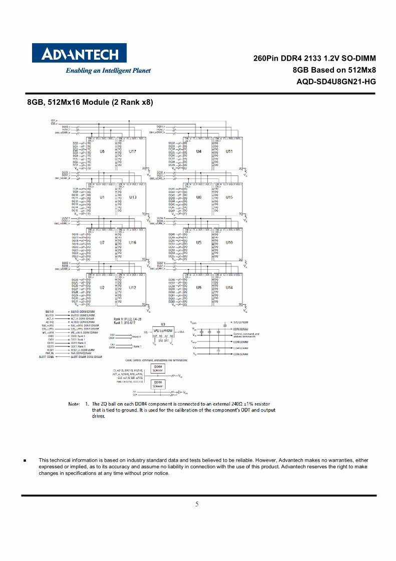
8GB, 512Mx16 Module (2 Rank x8)
This technical information is based on industry standard data and tests believed to be reliable. However, Advantech makes no warranties, either
expressed or implied, as to its accuracy and assume no liability in connection with the use of this product. Advantech reserves the right to make changes in specifications at any time without prior notice.
260Pin DDR4 2133 1.2V SO-DIMM 8GB Based on 512Mx8 AQD-SD4U8GN21-HG
6
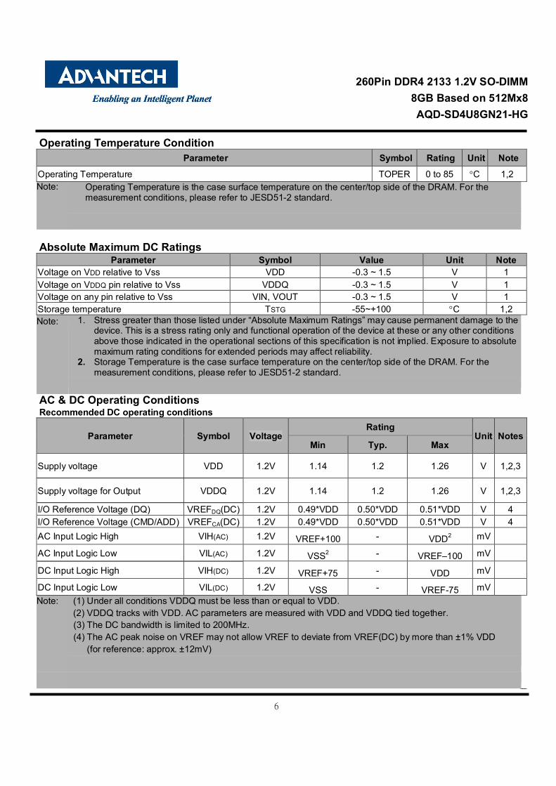
Operating Temperature Condition Parameter Symbol Rating Unit Note
Operating Temperature TOPER 0 to 85 C 1,2 Note: Operating Temperature is the case surface temperature on the center/top side of the DRAM. For the
measurement conditions, please refer to JESD51-2 standard.
Absolute Maximum DC Ratings
Parameter Symbol Value Unit Note Voltage on VDD relative to Vss VDD -0.3 ~ 1.5 V 1 Voltage on VDDQ pin relative to Vss VDDQ -0.3 ~ 1.5 V 1 Voltage on any pin relative to Vss VIN, VOUT -0.3 ~ 1.5 V 1 Storage temperature TSTG -55~+100 C 1,2 Note: 1. Stress greater than those listed under “Absolute Maximum Ratings” may cause permanent damage to the
device. This is a stress rating only and functional operation of the device at these or any other conditions above those indicated in the operational sections of this specification is not implied. Exposure to absolute maximum rating conditions for extended periods may affect reliability.
2. Storage Temperature is the case surface temperature on the center/top side of the DRAM. For the measurement conditions, please refer to JESD51-2 standard.
AC & DC Operating Conditions Recommended DC operating conditions
Parameter Symbol Voltage Rating
Unit Notes Min Typ. Max
Supply voltage VDD 1.2V 1.14 1.2 1.26 V 1,2,3
Supply voltage for Output VDDQ 1.2V 1.14 1.2 1.26 V 1,2,3
I/O Reference Voltage (DQ) VREFDQ(DC) 1.2V 0.49*VDD 0.50*VDD 0.51*VDD V 4 I/O Reference Voltage (CMD/ADD) VREFCA(DC) 1.2V 0.49*VDD 0.50*VDD 0.51*VDD V 4 AC Input Logic High VIH(AC) 1.2V VREF+100 - VDD2 mV
AC Input Logic Low VIL(AC) 1.2V VSS2 - VREF–100 mV
DC Input Logic High VIH(DC) 1.2V VREF+75 - VDD mV
DC Input Logic Low VIL(DC) 1.2V VSS - VREF-75 mV Note: (1) Under all conditions VDDQ must be less than or equal to VDD.
(2) VDDQ tracks with VDD. AC parameters are measured with VDD and VDDQ tied together. (3) The DC bandwidth is limited to 200MHz. (4) The AC peak noise on VREF may not allow VREF to deviate from VREF(DC) by more than ±1% VDD
(for reference: approx. ±12mV)

260Pin DDR4 2133 1.2V SO-DIMM 8GB Based on 512Mx8 AQD-SD4U8GN21-HG
7
IDD Specification parameters Definition - 8GB (2 Rank x8)
Parameter Symbol DDR4 2133 CL15 Unit
One bank ACTIVATE-PRECHARGE current IDD01 312 mA
One bank ACTIVATE-PRECHARGE, wordline boost, IPP current IPP01 41.6 mA
One Bank Active-Read-Precharge Current IDD11 376 mA
Precharge Standby Current IDD2N2 240 mA
Precharge standby ODT current IDD2NT1 232 mA
Precharge Power-Down Current IDD2P2 176 mA
Precharge Quiet Standby Current IDD2Q2 240 mA
Active standby current IDD3N2 432 mA
Active standby IPP current IPP3N2 41.6 mA
Active Power-Down Current IDD3P2 320 mA
Burst Read Current IDD4R1 752 mA
Burst write current IDD4W1 784 mA
Burst refresh current (1x REF) IDD5B1 1048 mA
Burst refresh IPP current (1x REF) IPP5B1 194.4 mA
Self refresh current: Normal temperature range (0–85°C) IDD6N2 176 mA
Self refresh current: Extended temperature range (0–95°C) IDD6E2 224 mA
Bank interleave read current IDD71 976 mA
Bank interleave read IPP current IPP71 111.2 mA
Maximum power-down current IDD82 80 mA Note:
1. One module rank in the active IDD/PP, the other rank in IDD2P/PP3N. 2. All ranks in this IDD/PP condition. 3.IDD current measure method and detail patterns are described on DDR4 component datasheet. Only for reference.
Timing Parameters & Specifications

260Pin DDR4 2133 1.2V SO-DIMM 8GB Based on 512Mx8 AQD-SD4U8GN21-HG
8
Parameter Symbol MIN MAX
Minimum Clock Cycle Time (DLL off mode) tCK (DLL_OFF) 8 - nsAverage Clock Period tCK(avg) psAverage high pulse width tCH(avg) 0.48 0.52 tCK(avg)Average low pulse width tCL(avg) 0.48 0.52 tCK(avg)
Absolute Clock Period tCK(abs)tCK(avg)min +
tJIT(per)min_to ttCK(avg)max +
tJIT(per)m ax_tottCK(avg)
Absolute clock HIGH pulse width tCH(abs) 0.45 - tCK(avg)Absolute clock LOW pulse width tCL(abs) 0.45 - tCK(avg)Clock Period Jitter- total JIT(per)_tot -0.1 0.1 UIClock Period Jitter- deterministic JIT(per)_dj TBD TBD UIClock Period Jitter during DLL locking period tJIT(per, lck) TBD TBD UICycle to Cycle Period Jitter tJIT(cc)_total UICycle to Cycle Period Jitter deterministic tJIT(cc)_dj UICycle to Cycle Period Jitter during DLL lockingperiod
tJIT(cc, lck) UI
Duty Cycle Jitter tJIT(duty) TBD TBD UICumulative error across 2 cycles tERR(2per) TBD TBD UICumulative error across 3 cycles tERR(3per) TBD TBD UICumulative error across 4 cycles tERR(4per) TBD TBD UICumulative error across 5 cycles tERR(5per) TBD TBD UICumulative error across 6 cycles tERR(6per) TBD TBD UICumulative error across 7 cycles tERR(7per) TBD TBD UICumulative error across 8 cycles tERR(8per) TBD TBD UICumulative error across 9 cycles tERR(9per) TBD TBD UICumulative error across 10 cycles tERR(10per) TBD TBD UICumulative error across 11 cycles tERR(11per) TBD TBD UICumulative error across 12 cycles tERR(12per) TBD TBD UICumulative error across n = 13, 14 . . . 49, 50cycles
tERR(nper) UI
CAS_n to CAS_n command delay for samebank group
tCCD_L 5 - nCK
CAS_n to CAS_n command delay for different bankgroup
tCCD_S 4 - nCK
ACTIVATE to ACTIVATE Command delay to differentbank group for 2KB page size
tRRD_S(2K) Max(4nCK,5.3ns) - nCK
ACTIVATE to ACTIVATE Command delay to differentbank group for 2KB page size
tRRD_S(1K) Max(4nCK,3.7ns) - nCK
ACTIVATE to ACTIVATE Command delay to differentbank group for 1/2KB page size
tRRD_S(1/2K) Max(4nCK,3.7ns) - nCK
ACTIVATE to ACTIVATE Command delay to samebank group for 2KB page size
tRRD_L(2K) Max(4nCK,6.4ns) - nCK
ACTIVATE to ACTIVATE Command delay to samebank group for 1KB page size
tRRD_L(1K) Max(4nCK,5.3ns) - nCK
ACTIVATE to ACTIVATE Command delay to samebank group for 1/2KB page size
tRRD_L(1/2K) Max(4nCK,5.3ns) - nCK
Four activate window for 2KB page size tFAW_2K 30 - nsFour activate window for 1KB page size tFAW_1K 21 - nsFour activate window for 1/2KB page size tFAW_1/2K 15 - nsDelay from start of internal write transaction tointernal read command for different bank group
tWTR_S max(2nCK,2.5ns) -
Delay from start of internal write transaction tointernal read command for same bank group
tWTR_L max(4nCK,7.5ns) -
Internal READ Command to PRECHARGE Commanddelay
tRTP max(4nCK,7.5ns) -
WRITE recovery time tWR 15 - ns
Write recovery time when CRC and DM are enabled tWR_CRC _DMtWR+max
(5nCK,3.75ns)- ns
delay from start of internal write transaction tointernal read command for different bank group withboth CRC and DM enabled
tWTR_S_CRC_DM
tWTR_S+max(5nCK,3.75ns)
- ns
delay from start of internal write transaction tointernal read command for same bank group withboth CRC and DM enabled
tWTR_L_CRC_DM
tWTR_L+max(5nCK,3.75ns)
- ns
DLL locking time tDLLK TBD - nCKMode Register Set command cycle time tMRD 8 - nCKMode Register Set command update delay tMOD max(24nCK,15ns) -Multi-Purpose Register Recovery Time tMPRR 1 - nCKMulti Purpose Register Write Recovery Time tWR_MPR tMOD (min) -
Command and Address Timing
tbd –(Definition tbd)
Clock Timing
UnitsSpeed DDR4-2133
0.2TBD
TBD
TBD
260Pin DDR4 2133 1.2V SO-DIMM 8GB Based on 512Mx8 AQD-SD4U8GN21-HG
9
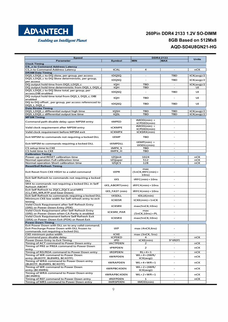
Parameter Symbol MIN MAX
CS_n to Command Address Latency tCAL 4 - nCK
DQS_t,DQS_c to DQ skew, per group, per access tDQSQ - TBD tCK(avg)/2DQS_t,DQS_c to DQ Skew deterministic, per group,per access
tDQSQ - TBD tCK(avg)/2
DQ output hold time from DQS_t,DQS_c tQH TBD - tCK(avg)/2DQ output hold time deterministic from DQS_t, DQS_c tQH TBD - UIDQS_t,DQS_c to DQ Skew total, per group, peraccess;DBI enabled
tDQSQ - TBD UI
DQ output hold time total from DQS_t, DQS_c; DBIenabled
tQH TBD - UI
DQ to DQ offset , per group, per access referenced toDQS_t, DQS_c
tDQSQ TBD TBD UI
DQS_t,DQS_c differential output high time tQSH TBD TBD tCK(avg)/2DQS_t,DQS_c differential output low time tQSL TBD TBD tCK(avg)/2
Command path disable delay upon MPSM entry tMPEDtMOD(min) +tCPDED(min)
-
Valid clock requirement after MPSM entry tCKMPEtMOD(min) +tCPDED(min)
-
Valid clock requirement before MPSM exit tCKMPX tCKSRX(min) -
Exit MPSM to commands not requiring a locked DLL tXMP TBD -
Exit MPSM to commands requiring a locked DLL tXMPDLLtXMP(min) +tXSDLL(min)
-
CS setup time to CKE tMPX_S TBD -CS hold time to CKE tMPX_H TBD -
Power-up and RESET calibration time tZQinit 1024 - nCKNormal operation Full calibration time tZQoper 512 - nCKNormal operation Short calibration time tZQCS 128 - nCK
Exit Reset from CKE HIGH to a valid command tXPRmax
(5nCK,tRFC(min)+10ns)
-
Exit Self Refresh to commands not requiring a lockedDLL
tXS tRFC(min)+10ns -
SRX to commands not requiring a locked DLL in SelfRefresh ABORT
tXS_ABORT(min) tRFC4(min)+10ns -
Exit Self Refresh to ZQCL,ZQCS and MRS(CL,CWL,WR,RTP and Gear Down)
tXS_FAST (min) tRFC4(min)+10ns -
Exit Self Refresh to commands requiring a locked DLL tXSDLL tDLLK(min) -Minimum CKE low width for Self refresh entry to exittiming
tCKESR tCKE(min)+1nCK -
Valid Clock Requirement after Self Refresh Entry(SRE) or Power-Down Entry (PDE)
tCKSRE max(5nCK,10ns) -
Valid Clock Requirement after Self Refresh Entry(SRE) or Power-Down when CA Parity is enabled
tCKSRE_PARmax
(5nCK,10ns)+PL-
Valid Clock Requirement before Self Refresh Exit(SRX) or Power-Down Exit (PDX) or Reset Exit
tCKSRX max(5nCK,10ns) -
Exit Power Down with DLL on to any valid command;Exit Precharge Power Down with DLL frozen tocommands not requiring a locked DLL
tXP max (4nCK,6ns) -
CKE minimum pulse width tCKE max (3nCK, 5ns) -Command pass disable delay tCPDED 4 - nCKPower Down Entry to Exit Timing tPD tCKE(min) 9*tREFITiming of ACT command to Power Down entry tACTPDEN 2 - nCKTiming of PRE or PREA command to Power Downentry
tPRPDEN 2 - nCK
Timing of RD/RDA command to Power Down entry tRDPDEN RL+4+1 - nCKTiming of WR command to Power Downentry (BL8OTF, BL8MRS, BC4OTF)
tWRPDENWL+4+(tWR/
tCK(avg))- nCK
Timing of WRA command to Power Down entry(BL8OTF, BL8MRS, BC4OTF)
tWRAPDEN WL+4+WR+1 - nCK
Timing of WR command to Power Downentry (BC4MRS)
tWRPBC4DENWL+2+(tWR/
tCK(avg))- nCK
Timing of WRA command to Power Down entry(BC4MRS)
tWRAPBC4DEN WL+2+WR+1 - nCK
Timing of REF command to Power Down entry tREFPDEN 1 - nCKTiming of MRS command to Power Down entry tMRSPDEN tMOD(min) -
CS_n to Command Address Latency
DRAM Data Timing
UnitsSpeed DDR4-2133
Clock Timing
Data Strobe Timing
MPSM Timing
Calibration Timing
Reset/Self Refresh Timing
Power Down Timing
260Pin DDR4 2133 1.2V SO-DIMM 8GB Based on 512Mx8 AQD-SD4U8GN21-HG
10
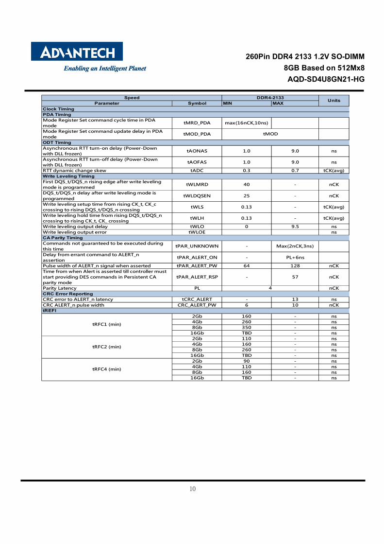
Parameter Symbol MIN MAX
Mode Register Set command cycle time in PDAmode
tMRD_PDA max(16nCK,10ns)
Mode Register Set command update delay in PDAmode
tMOD_PDA
Asynchronous RTT turn-on delay (Power-Downwith DLL frozen)
tAONAS 1.0 9.0 ns
Asynchronous RTT turn-off delay (Power-Downwith DLL frozen)
tAOFAS 1.0 9.0 ns
RTT dynamic change skew tADC 0.3 0.7 tCK(avg)
First DQS_t/DQS_n rising edge after write levelingmode is programmed
tWLMRD 40 - nCK
DQS_t/DQS_n delay after write leveling mode isprogrammed
tWLDQSEN 25 - nCK
Write leveling setup time from rising CK_t, CK_ccrossing to rising DQS_t/DQS_n crossing
tWLS 0.13 - tCK(avg)
Write leveling hold time from rising DQS_t/DQS_ncrossing to rising CK_t, CK_ crossing
tWLH 0.13 - tCK(avg)
Write leveling output delay tWLO 0 9.5 nsWrite leveling output error tWLOE ns
Commands not guaranteed to be executed duringthis time
tPAR_UNKNOWN - Max(2nCK,3ns)
Delay from errant command to ALERT_nassertion
tPAR_ALERT_ON - PL+6ns
Pulse width of ALERT_n signal when asserted tPAR_ALERT_PW 64 128 nCKTime from when Alert is asserted till controller muststart providing DES commands in Persistent CAparity mode
tPAR_ALERT_RSP - 57 nCK
Parity Latency PL nCK
CRC error to ALERT_n latency tCRC_ALERT - 13 nsCRC ALERT_n pulse width CRC_ALERT_PW 6 10 nCK
2Gb 160 - ns4Gb 260 - ns8Gb 350 - ns
16Gb TBD - ns2Gb 110 - ns4Gb 160 - ns8Gb 260 - ns
16Gb TBD - ns2Gb 90 - ns4Gb 110 - ns8Gb 160 - ns
16Gb TBD - ns
ODT Timing
Write Leveling Timing
CA Parity Timing
CRC Error Reporting
tREFI
tRFC1 (min)
tRFC2 (min)
tRFC4 (min)
Clock Timing
tMOD
4
PDA Timing
UnitsSpeed DDR4-2133
260Pin DDR4 2133 1.2V SO-DIMM 8GB Based on 512Mx8 AQD-SD4U8GN21-HG
11
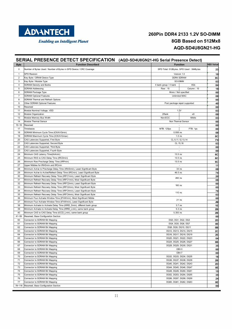
SERIAL PRESENCE DETECT SPECIFICATION (AQD-SD4U8GN21-HG Serial Presence Detect) Byte HEX Value
0 23
1 102 0C3 034 4 bank group / 4 bank 4Gb 845 Row : 15 Column : 10 196 007 088 009 40
10 0011 0312 2Rank x8 0913 Non-ECC 64bits 0314 00
15~16 0017 MTB: 125ps FTB: 1ps 0018 0.938 ns 0819 1.5 ns 0C20 F421 0322 0023 0024 13.5 ns 6C25 13.5 ns 6C26 13.5 ns 6C27 1128 33 ns 0829 46.5 ns 7430 2031 0832 0033 0534 7035 0336 0037 A838 3.7 ns 1E39 5.3 ns 2B40 5.355 ns 2B
41~59 0060 2D61 0E62 0B63 2C64 2E65 0466 0B67 3568 0069 0070 1671 2B72 2D73 0E74 1575 3576 2477 0E
78~116 00
Connector to SDRAM Bit Mapping
Connector to SDRAM Bit Mapping
DQ60, DQ61, DQ62, DQ63
CB0-3
CB4-7
DQ32, DQ33, DQ34, DQ35
DQ36, DQ37, DQ38, DQ39DQ40, DQ41, DQ42, DQ43
DQ44, DQ45, DQ46, DQ47
DQ48, DQ49, DQ50, DQ51
DQ52, DQ53, DQ54, DQ55
DQ56, DQ57, DQ58, DQ59
Connector to SDRAM Bit Mapping
Connector to SDRAM Bit Mapping
Connector to SDRAM Bit Mapping
Connector to SDRAM Bit Mapping
Connector to SDRAM Bit Mapping
Connector to SDRAM Bit MappingConnector to SDRAM Bit Mapping
Connector to SDRAM Bit Mapping
Connector to SDRAM Bit Mapping
Minimum CAS Latency Time(tAAmin)
Minimum RAS to CAS Delay Time (tRCDmin)
Upper Nibbles for tRASmin and tRCmin
Other SDRAM Optional Features Post package repair supported
Connector to SDRAM Bit Mapping
CL 9,11,12,13,14
Module Nominal Voltage, VDD
SDRAM Minimum Cycle Time (tCKAVGmin)
SDRAM Maximum Cycle Time (tCKAVGmax)
Key Byte / Module TypeSDRAM Density and Banks
CAS Latencies Supported, First ByteCAS Latencies Supported, Second Byte
SDRAM Addressing
SDRAM Package Type
Reserved
SDRAM Thermal and Refresh Options
SDRAM Optional Features
Timebases
SPD Revision
SO-DIMM
CL 15,16
-
Mono / Not specified
Minimum Active to Active/Refresh Delay Time (tRCmin), Least Significant Byte
Minimum Refresh Recovery Delay Time (tRFC1min), Most Significant Byte
Minimum Refresh Recovery Delay Time (tRFC1min), Least Significant Byte
Minimum Activate to Activate Delay Time (tRRD_Smin), different bank group
Minimum Refresh Recovery Delay Time (tRFC4min), Least Significant Byte
Reserved, Base Configuration Section
SPD Total: 512Bytes, SPD Used : 384Bytes
Version 1.0
DDR4 SDRAM
Function
Key Byte / DRAM Device Type
Function Described
110
Number of Bytes Used / Number of Bytes in SPD Device / CRC Coverage
nsMinimum Refresh Recovery Delay Time (tRFC4min), Most Significant Byte
Unlimited MAC
-
-
1.2VModule Organization
Module Thermal Sensor
Module Memory Bus Width
Non Thermal Sensor
Reserved -
CAS Latencies Supported, Third Byte -
CAS Latencies Supported, Fourth Byte -
Minimum Refresh Recovery Delay Time (tRFC2min), Least Significant Byte
Minimum Refresh Recovery Delay Time (tRFC2min), Most Significant Byte160 ns
260 ns
Minimum Row Precharge Delay Time (tRPmin)
Minimum Active to Precharge Delay Time (tRASmin), Least Significant Byte
Minimum Four Activate Window Time (tFAWmin), Most Significant Nibble
Minimum Four Activate Window Time (tFAWmin), Least Significant Byte21 ns
Minimum Activate to Activate Delay Time (tRRD_Lmin), same bank group
Minimum CAS to CAS Delay Time (tCCD_Lmin), same bank group
Reserved, Base Configuration Section -
Connector to SDRAM Bit Mapping
DQ0, DQ1, DQ2, DQ3
DQ4, DQ5, DQ6, DQ7
DQ8, DQ9, DQ10, DQ11
DQ12, DQ13, DQ14, DQ15DQ16, DQ17, DQ18, DQ19
DQ20, DQ21, DQ22, DQ23
DQ24, DQ25, DQ26, DQ27
DQ28, DQ29, DQ30, DQ31
Connector to SDRAM Bit Mapping
Connector to SDRAM Bit Mapping
Connector to SDRAM Bit MappingConnector to SDRAM Bit Mapping
Connector to SDRAM Bit Mapping
-
260Pin DDR4 2133 1.2V SO-DIMM 8GB Based on 512Mx8 AQD-SD4U8GN21-HG
12
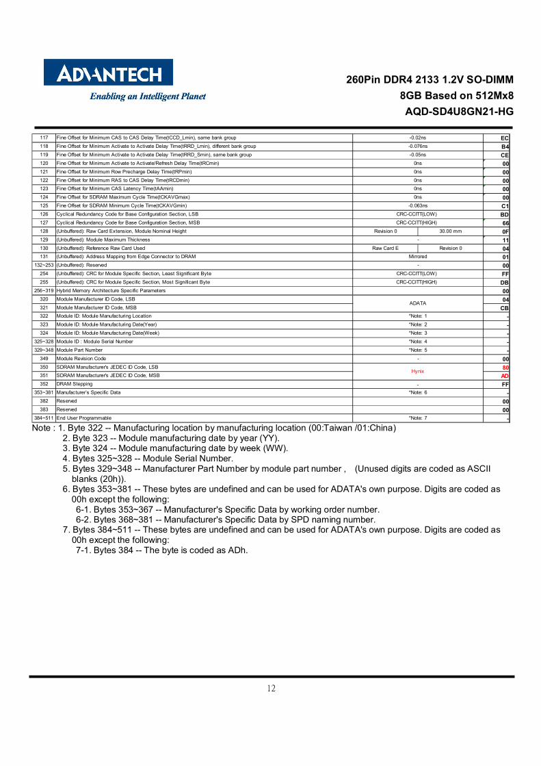
117 EC118 B4119 CE120 00121 00122 00123 00124 00125 C1126 BD127 66128 Revision 0 30.00 mm 0F129 11130 Raw Card E Revision 0 04131 01
132~253 00254 FF255 DB
256~319 00320 04321 CB322 -323 -324 -
325~328 -329~348 -
349 00350 80351 AD352 FF
353~381 -382 00383 00
384~511 -
ADATA
*Note: 1
*Note: 2
Module ID: Module Manufacturing Location
Module Revision Code -
Module Part Number *Note: 5
SDRAM Manufacturer's JEDEC ID Code, LSBHynix
SDRAM Manufacturer's JEDEC ID Code, MSB
Manufacturer’s Specific Data *Note: 6
CRC-CCITT(LOW)
*Note: 3
Module ID: Module Manufacturing Date(Year)
Module ID: Module Manufacturing Date(Week)
(Unbuffered): Reference Raw Card Used
(Unbuffered): Module Maximum Thickness -
(Unbuffered): Address Mapping from Edge Connector to DRAM Mirrored
(Unbuffered): Reserved -
(Unbuffered): CRC for Module Specific Section, Least Significant Byte
(Unbuffered): CRC for Module Specific Section, Most Significant Byte
Hybrid Memory Architecture Specific Parameters
Module Manufacturer ID Code, MSB
Cyclical Redundancy Code for Base Configuration Section, LSB
Module Manufacturer ID Code, LSB
-0.02nsFine Offset for Minimum CAS to CAS Delay Time(tCCD_Lmin), same bank group
Fine Offset for Minimum Row Precharge Delay Time(tRPmin) 0ns
Fine Offset for Minimum RAS to CAS Delay Time(tRCDmin) 0nsFine Offset for Minimum CAS Latency Time(tAAmin) 0ns
Fine Offset for SDRAM Maximum Cycle Time(tCKAVGmax) 0ns
Fine Offset for Minimum Activate to Activate Delay Time(tRRD_Lmin), different bank group -0.076ns
Fine Offset for Minimum Activate to Activate Delay Time(tRRD_Smin), same bank group -0.05ns
End User Programmable
DRAM Stepping
*Note: 7
CRC-CCITT(LOW)
CRC-CCITT(HIGH)
Fine Offset for SDRAM Minimum Cycle Time(tCKAVGmin) -0.063ns
-
Reserved
Reserved
*Note: 4
CRC-CCITT(HIGH) Cyclical Redundancy Code for Base Configuration Section, MSB
(Unbuffered): Raw Card Extension, Module Nominal Height
Module ID : Module Serial Number
Fine Offset for Minimum Activate to Activate/Refresh Delay Time(tRCmin) 0ns
Note : 1. Byte 322 -- Manufacturing location by manufacturing location (00:Taiwan /01:China) 2. Byte 323 -- Module manufacturing date by year (YY). 3. Byte 324 -- Module manufacturing date by week (WW). 4. Bytes 325~328 -- Module Serial Number. 5. Bytes 329~348 -- Manufacturer Part Number by module part number , (Unused digits are coded as ASCII
blanks (20h)). 6. Bytes 353~381 -- These bytes are undefined and can be used for ADATA's own purpose. Digits are coded as
00h except the following: 6-1. Bytes 353~367 -- Manufacturer's Specific Data by working order number. 6-2. Bytes 368~381 -- Manufacturer's Specific Data by SPD naming number.
7. Bytes 384~511 -- These bytes are undefined and can be used for ADATA's own purpose. Digits are coded as 00h except the following:
7-1. Bytes 384 -- The byte is coded as ADh.


![Chapter 9 Tools and Resources for Evaluating the ... 9... · Exhibit 1: Data Elements for Evaluating and ... aQd reOLabOe VtaQdardL]ed teVtV aQd JradXatLoQ drop oXt aQd reteQtLoQ](https://img.pdfslide.us/doc/110x75/5af3a36a7f8b9a95468cdaa4/chapter-9-tools-and-resources-for-evaluating-the-9exhibit-1-data-elements.jpg)