Embed Size (px)
Citation preview

apricot Service
Manual
apricot
Service Manual

PREFACE
This service manual contains all the information required for the after-sales service that is required to maintain the high quality and reliability of the ACT APRICOT executive micro-computer.
It is assumed throughout this manual that all service personnel involved in the maintenance of the ACT APRICOT already have an in-depth knowledge of digital electronics, with particular emphasis on micro-computer techniques.
This manual contains information relevant to the total APRICOT range. Illustrations and photographs used are of the twin floppy drive version. Please refer to relevant sections for variations.
ACT (International) Ltd. wishes to acknowledge the co-operation of the following companies for giving their permission in allowing the reproduction of their proprietry information:
SONY (UK) LTD. National Panasonic (UK) Ltd. Texas Instruments Ltd. QED (Product Design) Ltd.
The information in this manual is subject to change without notice and does not represent a commitment on the part of ACT. The software description in this manual is furnished under a license agreement. The software may be used or copied only in accordance with the terms of the agreement. It is against the law to copy any disk supplied for any purpose other than the purchaser's personal use.
© Applied Computer Techniques PLC 1983.

CONTENTS
Chapter
1
2
3
4
5
6
7
8
9
10
11
General description Specification
Installation
Safety precautions
Recommended tools and equipment
Assembly and disassembly
Electrical system
Electronic system Memory map
Set-up procedures
Trouble-shooting Diagnostic programs
Expansion Boards
Winchester
Appendix
A Monitor
B Disk drive
C Parts list
D PSU
E Circuit diagrams, wiring diagrams
Index
I INDEX
Assembly and Features 1.2 Disassembly 5.1 Fuses 3.2
AC Sub Assembly 6.3 Floppy Disk Controller 7.13 Async Cable
Installation 2.1 Connection 6.19 Interconnection
Block Diagram Apricot 7.22 Diagram 6.2 Conversion 240V -115V 6.4 I/O Section 7.11 Connectors Pin-Outs 6.6 I/O Port Address 7.20 Circuit Diagrams E1 I/C Catalogue 7.23
Disassembly Modem Cable Rear Panel 5.3 Connection 6.19 AC Sub Assembly 5.4 Memory 7.6 Motherboard 5.5 Memory Map 7.38 Chassis Bridge Monitor A.1 Assembly 5.6 Mnemonics 7.34 Disk Drives 5.7 Parts Description 1.5 Front Bezel and Door 5.8 Main Chassis 5.9 Printer Cable
Power Supply 5.9 Parallel 6.20
Handle 5.9 Serial 6.21
Speaker 5.9 Processor Structure 7.7
Monitor 5.10 Parallel Interface 7.14
Keyboard 5.11 Parts List C.1
5.12 Power Supply E.1
5.13 Recommended Tools 4.1 Diagnostic Recommended
Boot Prom Equipment 4.1 Documentation Error Codes 9.1 Specification 1.4 Programs 9.5 Safety Precautions 3.1 Disk Drive B.1 System Outline 7.3
Electrical System 6.1 Sound Generator 7.11 Serial Interface 7.18
Earthing 6.5 Set-Up Procedure 8.1 Expansion Information 6.16 Electronic System 7.1 Timer 7.16

,---1 _ _ G_E_N_E_RA_L_D_E_SC_RIPT __ I_O_N_----.l10
I Features
IT . Specifications
ill Individual units
GENERAL DESCRIPTION rn I FEATURES
Processor architecture
8086 running at 5mHz 8089 I/O processor 8087 Optional Maths co-processor
Memory
256 Kbytes expandable to 768 Kbytes
Mass storage
One or two 3.5" Sony mirco-floppy disk drives-315 Kbytes each or One or two 3.5" Sony double sided micro-floppy disk drives-360 Kbytes each side
Display
1/0
9" green P39 phosphor with antiglare filter 80 characters x 25 lines Resolution: 800 x 400 pixels
1 x RS232 (V-24) serial port 1 x 8-bit Centronics parallel printer port Optional on-board modem with auto-dial 2 x expansion slots 1 x "Mouse" port
Keyboard
Soft QWERTY keyboard with 8 fixed function keys and 6 touch sensitive keys labelled by LCD MicroScreen (tm). Built-in 4 function calculator. Time/Date display with battery back-up.
Safety/radiation standards
Meets UL VDE BS415 CSA FCC-B
1~;~l~1rll GENERAL DESCRIPTION
II SPECIFICATION
Physical dimensions
Systems box: 16.5" (43.Scm) wide x 4" (10.6cm) high x 12.5" (33cm) deep
Monitor: 10.5" (27.7cm) wide x 8.5" (22.Scm) high x 10" (26.4cm) deep
Keyboard: 16" (42cm) wide x 2" (S.3cm) high x 7" (18.Scm) deep
Weight
Systems box: 14.21bs (6.5 kg) Monitor: 9.11bs (4.1 kg) Keyboard: 3.31bs (1.5 kg)
Power requirements
200 to 240 VAC 47 to 63 Hz or 100 to 125 VAC 47 to 63 Hz
Power consumption
100Wat 11SV or 230V input
Temperature range
Operating: 5 to 37°C Storage: -20 to 60°C
Humidity
Operating: 20 to 80% RH @ 29°C non-condensing
G£N£FAL D£SCR{P'1'ION m Ul INDl\TlDtJAL tJNffS 1. Monitor
2. system Unit 3. Reyboard 4. Microscreen un
\ s. Touch Sensitive Reys \I 6. fiJ{ed function Reys
7. Door 8. Bri~btness control
2
~~ii~iiilll;I~~'9' Video Cable ~ \0. Reyboard Cable
11. ReyboarO connector 12. Centronics connector 13. Serial connector 14. Video connector
6
15. Mouse port 16. Mains switcb 17. Fuse 18. Mains lnpUt
16
18
."rr-- -17
9
I~:~}I GENERAL DESCRIPTION
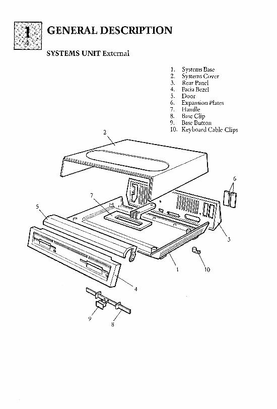
SYSTEMS UNIT External
1. Systems Base 2. Systems Cover 3. Rear Panel 4. Facia Bezel 5. Door 6. Expansion Plates 7. Handle 8. Base Clip 9. Base Button
2 10. Keyboard Cable Clips
3
~4 8
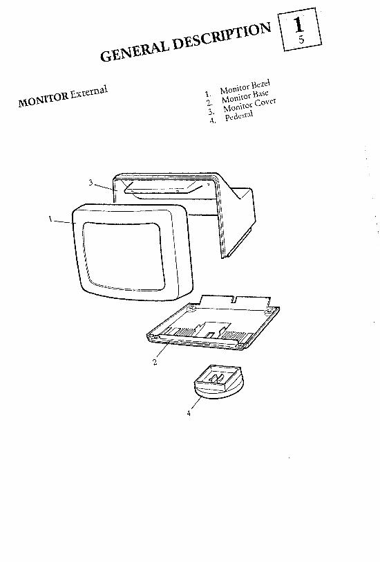
G£N£W\.L D£SCWYf\ON ill ~O~rroR £,)ttern
a1 1. Monitor Bezel 2. Monitor Base 3. Monitor Covcr 4. PcJcst~\
1
I'fz!~/I GENERAL DESCRIPTION
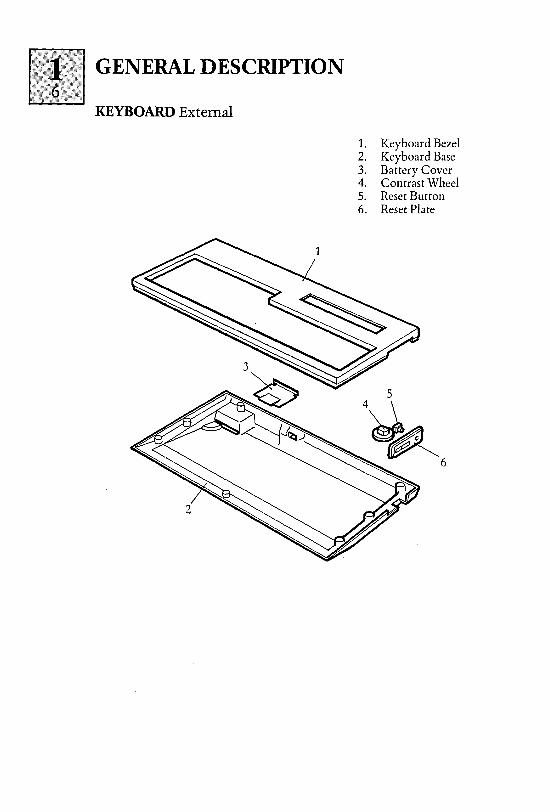
KEYBOARD External
1. Keyboard Bezel 2. Keyboard Base 3. Battery Cover 4. Contrast Wheel 5. Reset Button 6. Reset Plate
5
4~~ 6
GENERAL DESCRIPTION
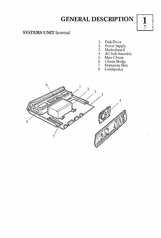
SYSTEMS UNIT Internal
1. Disk Drive 2. Power Supply 3. ~otherboard 4. AC Sub-Assembly 5. ~ain Chassis 6. Chassis Bridge 7. Expansion Slots 8. Loudspeaker
li:J'wl GENERAL DESCRIPTION
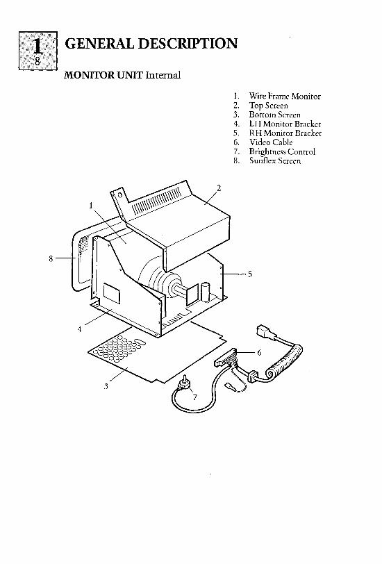
MONITOR UNIT Internal
1. Wire Frame Monitor 2. Top Screen 3. Bottom Screen 4. LH Monitor Bracket 5. RH Monitor Bracket 6. Video Cable 7. Brightness Control 8. Sunflex Screen
8
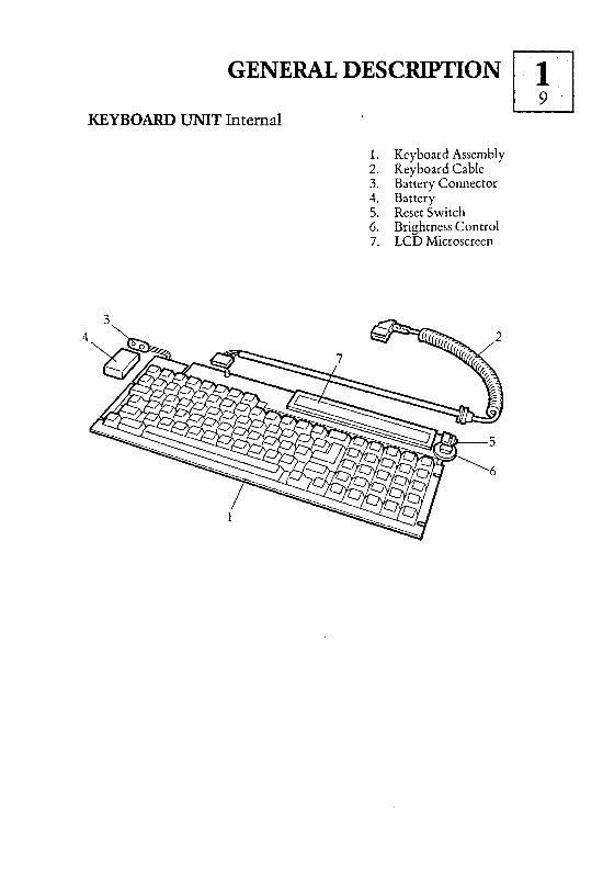
GENERAL DESCRIPTION rn KEYBOARD UNIT Internal .
1. Keyboard Assembly 2. Keyboard Cable 3. Battery Connector 4. Battery 5. Reset Switch 6. Brightness Control 7. LCD Microscreen

,---.•. IN_SL_~_L_L_AT_I_O_N ____ ----,I ~

INSTALLATION W Each computer is carefully adjusted and strictly
inspected before it leaves the factory.
Correct installation is extremely important to maintain the high degree of reliability and performance in-built in the machine.
Note the following recommendations:
1. Ensure the line voltage is within the voltage marked on the outside of the systems unit.
2. To maintain data integrity, the computer should be operated in an electrical environment not subject to large voltage transients on the line. A normal office supply is perfectly adequate. Avoid close proximity with heavy industrial machinery such as presses, arc welders, etc.
3. Ensure the operating temperature is not exceeded, and that the temperature of the machine is allowed to stabilise (for approximately 30 mins.) if it is moved from one extreme to another.
4. Do not obstruct any of the ventilation grills.
5.
6.
Under no circumstances must any liquid be allowed to enter any of the units.
Operating the machine in an abnormally dusty atmosphere will substantially reduce the life of the disk drive and the media.
7. The plastic case of the machine can be cleaned with a damp cloth. Under no circumstances use an abrasive cleanser or solvent.
8. Although the Sony micro floppy disks are extremely robust, a few precautions will ensure a long and trouble-free life:
(i) Keep auto shutter closed at all times.
(ii) Never touch the oxide surface.
(iii) Do not exceed their temperature range (IO°C to 60°C).
(iv) Do not expose the disks to any magnetic field.
(v) Do not attempt to clean the disk surface. This may result in damage to the disk drive heads.

~S_AF_E_T_Y_P_RE_C_A_U_T_IO_N_S __ ----II~ I General Safety Precautions
II Fuses
ill Power Supply

SAFETY PRECAUTIONS rn I GENERAL SAFETY PRECAUTIONS
1. The ACT Apricot has been designed to meet all international safety standards in~luding UL, VDE, BS41S, CSA and FCC-B radiation standards.
2. It is recommended that installation of any expansion boards or modifications, be carried out by an authorised dealer - the end user should not dismantle the units.
3. Replacement parts should be of the type and rating specified by the manufacturer, to prevent the risk of shock or fire.
Refer to appendix A for important safety precautions on the monitor.
4. All earth connections should be maintained to the original specification, refer to Chapter 6.
rx":"~\;1 SAFETY PRECAUTIONS
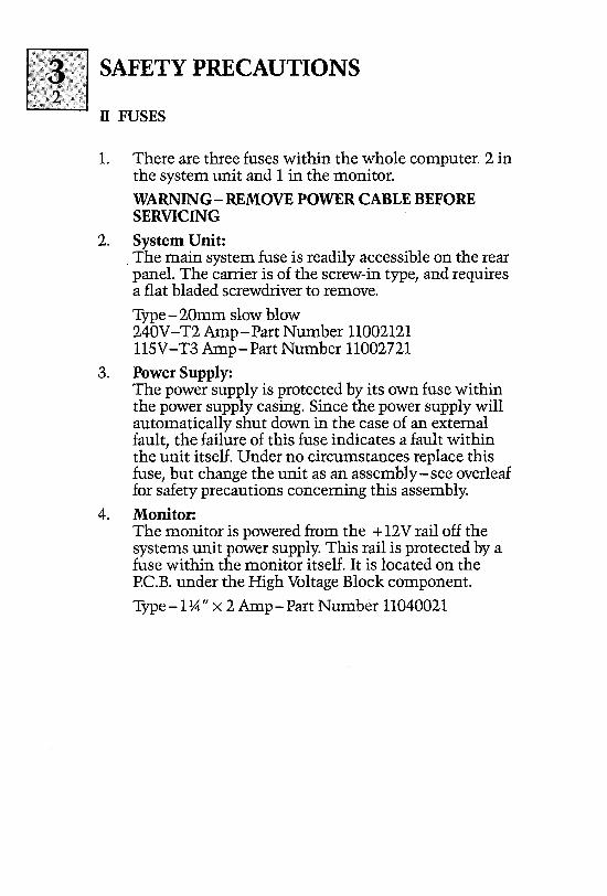
n FUSES
1. There are three fuses within the whole computer. 2 in the system unit and 1 in the monitor.
WARNING- REMOVE POWER CABLE BEFORE SERVICING
2. System Unit: . The main system fuse is readily accessible on the rear panel. The carrier is of the screw-in type, and requires a flat bladed screwdriver to remove.
Type - 20mm slow blow 240V-T2 Amp-Part Number 11002121 115V-T3 Amp-Part Number 11002721
3. Power Supply: The power supply is protected by its own fuse within the power supply casing. Since the power supply will automatically shut down in the case of an external fault, the failure of this fuse indicates a fault within the unit itself. Under no circumstances replace this fuse, but change the unit as an assembly-see overleaf for safety precautions concerning this assembly.
4. Monitor: The monitor is powered from the + 12V rail off the systems unit power supply. This rail is protected by a fuse within the monitor itself. It is located on the p.e.B. under the High Voltage Block component.
Type-1~" x 2 Amp-Part Number 11040021

SAFETY PRECAUTIONS rn ill POWER SUPPLY
The ACT Apricot utilizes an ASTEC AC9335 power supply module. Appendix D gives a full specification of the unit.
The unit is of the switch-mode type, and very high voltages are present throughout. If it is envisaged that any kind of testing or servicing be carried out, with the top cover removed, the following precautions should be taken:
1. Use 1:1 isolation transformer in the line.
2. Service only in a "high-voltage" test area.
3. Incorporate an emergency off switch.
4. Disconnect all earths from test equipment.
5. Take every precaution to minimise shock hazard.
It is highly recommended that in the case of failure, this unit should be returned to the distributor for repair.

RECOMMENDED 1m L....--TO_O_L_S_A_N_D_E_Q_V_IP_M_EN_T_'_----a LJ
RECOMMENDED m TOOLS AND EQUIPMENT LLJ
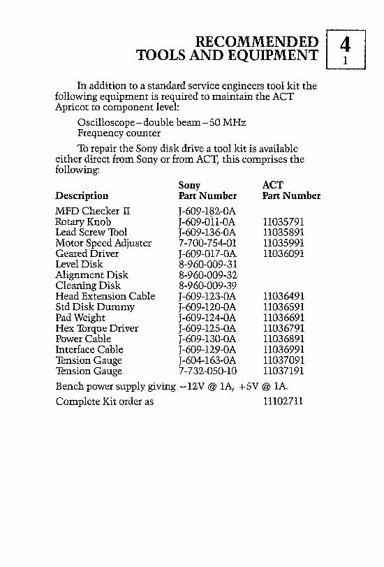
In addition to a standard service engineers tool kit the following equipment is required to maintain the ACT Apricot to component level:
Oscilloscope - double beam - 50 MHz Frequency counter
To repair the Sony disk drive a tool kit is available either direct from Sony or from ACT, this comprises the following:
Sony Description Part Number
MFD Checker II J-609-1~2-0A Rotary Knob J-609-011-0A Lead Screw Tool J-609-136-0A Motor Speed Adjuster 7 -700-754-01 Geared Driver J-609-017-0A Level Disk 8-960-009-31 Alignment Disk 8-960-009-32 Cleaning Disk 8-960-009-39
ACT Part Number
11035791 11035891 11035991 11036091
Head Extension Cable J-609-123-0A 11036491 Std Disk Dummy J-609-120-0A 11036591 Pad Weight J-609-124-0A 11036691 Hex Torque Driver J-609-125-0A 11036791 Power Cable J-609-130-0A 11036891 Interface Cable J-609-129-0A 11036991 Tension Gauge J-604-163-0A 11037091 Tension Gauge 7-732-050-10 11037191
Bench power supply giving -12V @ lA, + 5V @ 1A.
Complete Kit order as 11102711

<----A_S_S_EM_B_LY_AN_D ____ ---a'i m _ DISASSEMBLY _ ~
I Rear Panel and Top Cover
II AC Sub Assembly
ill Motherboard
IV Chassis Bridge
V Disk Drives
VI Front Bezel and Door
VII Main Chassis, Power Supply, Loudspeaker and Handle
Vill Monitor
IX Keyboard

ASSEMBLY AND DISASSEMBLY
GENERAL RECOMMENDATIONS
1. Disconnect from mains supply before disassembling machine.
2. Unless specifically noted, reassembly is the reverse of disassembly and will not be described unless necessary.
3. Do not mix screws (length, diameter).
4. A number in parenthesis thus (4) indicates the number of screws to be slackened or removed to remove that particular part.
I?I ASSEMBLY AND DISASSEMBLY
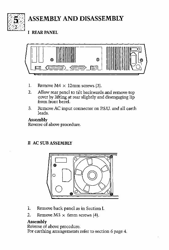
I REARPANEL
@) ~~~ m~~ @) "-- ~
(QJ (II II) c: c::=::::==:=J ~ ~
1. Remove M4 x 12mm screws (3).
2. Allow rear panel to tilt backwards and remove top cover by lifting at rear slightly and disengaging lip from front bezel.
3. Remove AC input connector on P.S.U. and all earth leads.
Assembly Reverse of above procedure.
II AC SUB ASSEMBLY
1. Remove back panel as in Section I.
2. RemoveM3 x 6mmscrews (4).
Assembly Reverse of above procedure. For earthing arrangements refer to section 6 page 4.
..
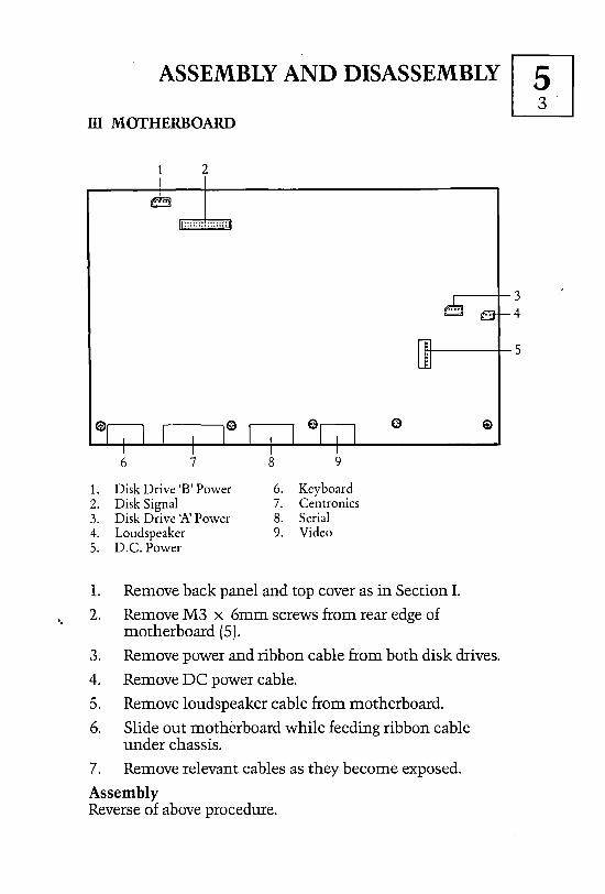
ASSEMBLY AND DISASSEMBLY rn m MOTHERBOARD
2
................
.....---f-3 4
~----t-5
6 7 8 9
1. Disk Drive 'B' Power 6. Keyboard 2. Disk Signal 7. Centronics 3. Disk Drive 'A' Power 8. Serial 4. Loudspeaker 9. Video 5. D.C. Power
1. Remove back panel and top cover as in Section I.
2. Remove M3 x 6mm screws from rear edge of motherboard (5 J.
3. Remove power and ribbon cable from both disk drives.
4. Remove DC power cable.
5. Remove loudspeaker cable from motherboard.
6. Slide out motherboard while feeding ribbon cable under chassis.
7. Remove relevant cables as they become exposed.
Assembly Reverse of above procedure.

Ii!!? I ASSEMBLY AND DISASSEMBLY
IV CHASSIS BRIDGE ASSEMBLY
(i) Remove rear panel and top cover as in Section 1.
(ii) Disconnect power and ribbon cables from disk drives.
(iii) Slacken M3 x 6mm screws (4).
(iv) Lift chassis bridge assembly away from main chassis.
Assembly Reverse of above procedure.
ASSEMBLY AND DISASSEMBLY
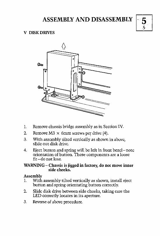
V DISK DRIVES
o
1. Remove chassis bridge assembly as in Section 'IV.
2. Remove M3 x 6mm screws pe! drive (4).
3. With assembly tilted vertically as shown in above, slide out disk drive.
4. Eject button and spring will be left in front bezel-note orientation of button. These components are a loose fit-do not lose.
WARNING- Chassis is jigged in factory, do not move inner side cheeks.
Assembly 1. With assembly tilted vertically as shown, install eject
button and spring orientating button correctly.
2. Slide disk drive between side cheeks, taking care the LED correctly locates in its aperture.
3. Reverse of above procedure.
I~ ... 1 ASSEMBLY AND DISASSEMBLY
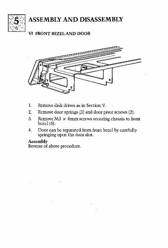
VI FRONT BEZEL AND DOOR
1. Remove disk drives as in Section V.
2. Remove door springs (2) and door pivot screws (2).
3. Remove M3 x 6mm screws securing chassis to front bezel (6).
4. Door can be separated from front bezel by carefully springing open the door slot.
Assembly Reverse of above procedure.
ASSEMBLY AND DISASSEMBLY
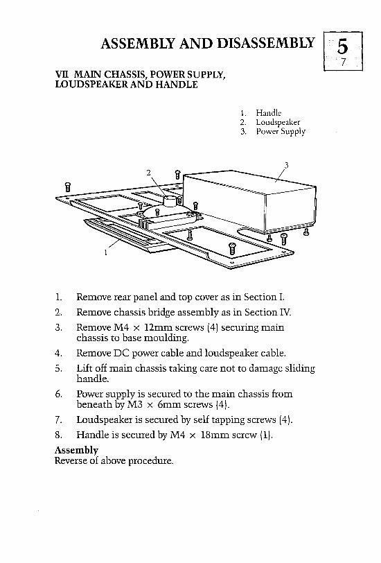
vn MAIN CHASSIS, POWER SUPPLY, LOUDSPEAKER AND HANDLE
1. Handle 2. Loudspeaker 3. Power Supply
3
1. Remove rear panel and top cover as in Section I.
2. Remove chassis bridge assembly as in Section IV.
3. Remove M4 x I2mm screws (4) securing main chassis to base moulding.
4. Remove DC power cable and loudspeaker cable.
S. Lift off main chassis taking care not to damage sliding handle.
6. Power supply is secured to the main chassis from beneath by M3 x 6mm screws (4).
7. Loudspeaker is secured by self tapping screws (4).
S. Handle is secured by M4 x ISmm screw (I).
Assembly Reverse of above procedure.
I;J~;~:;I ASSEMBLY AND DISASSEMBLY
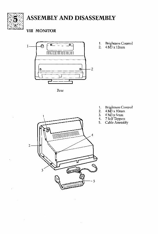
vm MONITOR
B ( Q o ~ 1. Brightness Control 2. 4M3x 12mm
rrrr rrrrrrrrrrrrrrr rrrrrrrrrr
10 ol-f-- 2 \
;--l.\ LJ II-...I L
I I
Rear
1. Brightness Control 2. 4M3x lOmm 3. 4M3x6mm 4. 7 Self Tappers 5. Cable Assembly
2

ASSEMBLY AND DISASSEMBLY W 1. Remove brightness knob.
2. Remove top cover - M3 x 12mm screws - 2 at rear of monitor, 2 within handle recess (4).
3. Slacken self tapping screws (8) securing top metal screen.
4. Remove brightness control from top screen.
5. Unplug cable assembly, and disengage grommet from base moulding. Detach screen from chassis (1).
6. Remove M3 x 10mm screws securing front bezel to side cheeks (4).
7. Remove M2 x 6mm screws securing base moulding to chassis (4).
8. Lift away front bezel together with Sunflex screen.
9. Lift away side cheeks and monitor assembly from base moulding.
10. Monitor assembly has a bottom screen plate secured by self tapping screws (2).
Assembly Reverse of above procedure.
li~1 ASSEMBLY AND DISASSEMBLY
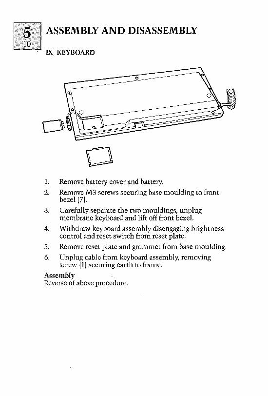
IX. KEYBOARD
o 1. Remove battery cover and battery.
2. Remove M3 screws securing base moulding to front bezel (7).
3. Carefully separate the two mouldings, unplug membrane keyboard and lift off front bezel.
4. Withdraw keyboard assembly disengaging brightness control and reset switch from reset plate.
5. Remove reset plate and grommet from base moulding.
6. Unplug cable from keyboard assembly, removing screw (1) securing earth to frame.
Assembly Reverse of above procedure.
ASSEMBLY AND DISASSEM"BLY m L1iJ
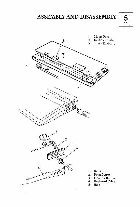
1. Mouse Port 2. Keyboard Cable 3. Touch Keyboard
2-~
4
1. Reset Plate 2. Reset Button 3. Contrast Button 4. Keyboard Cable 5. Base
&-\_, E_L_E_C_TRI_C_A_L-.;....SY_S_T_E_~ __ -----II ~ I Interconnection Diagram
II AC Sub Assembly
III Conversion from 240V to 11SV
IV Earthing
V Cable Connection
VI Expansion Details
VII Async Cable
VIII Printers
ELECTRICAL SYSTEM
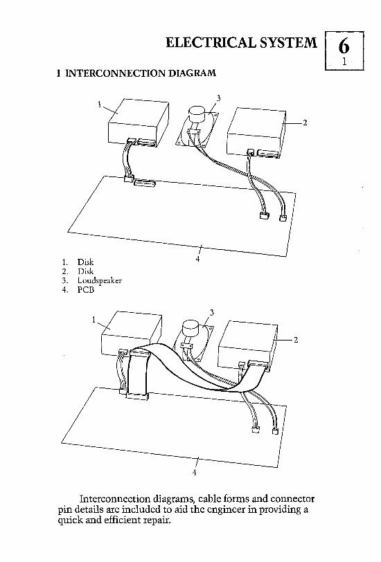
I INTERCONNECTION DIAGRAM
3
2
1. Disk 2. Disk 3. Loudspeaker 4. PCB
2
4
Interconnection diagrams, cable forms and connector pin details are included to aid the engineer in providing a quick and efficient repair.

\ttii ELECTRICAL SYSTEM
o.v. TO POWER SUPPLY CASING
----- -l
POWER SUPPLY
I I I I
D.C.POWER
8;:::::::::::;:===== MAINS IN from AC Sub-Chassis
______ .J
IT AC SUB ASSEMBLY
This assembly contains four parts which are mounted onto a metal plate. Two of these parts are dependent on the mains input voltage. Refer to section III of this chapter for conversion details.
(a) The fan is a 12W device and designed to extract air from the unit.
(b) The switch will be illuminated when the unit is switched on.
(c) The fuseholder is a 20mm type and made from fire retardant material.
(d) The filter has been designed to both reduce mains transients, and reduce the reflected noise from the power supply back to the mains. It will accept a standard IEC mains connector.·
This chapter also contains the correct earthing diagram which should be adhered to at all times.
Refer to appendix E for the AC wiring diagram.
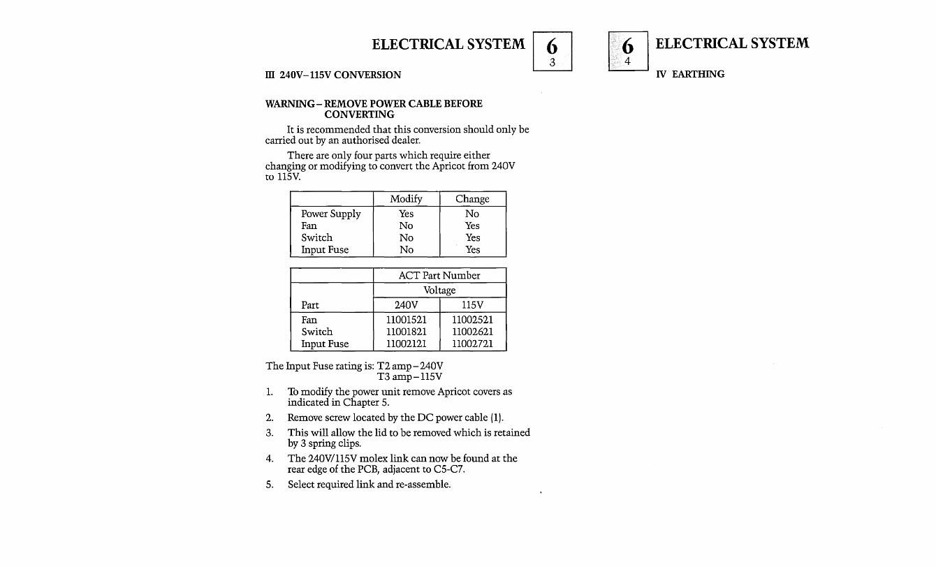
ELECTRICAL SYSTEM W ill 240V-115V CONVERSION
WARNING- REMOVE POWER CABLE BEFORE CONVERTING
It is recommended that this conversion should only be carried out by an authorised dealer.
There are only four parts which require either changing or modifying to convert the Apricot from 240V to 115V.
Modify Change
Power Supply Yes No Fan No Yes Switch No Yes Input Fuse No Yes
ACT Part Number Voltage
Part 240V
Fan 11001521 Switch 11001821 Input Fuse 11002121
The Input Fuse rating is: T2 amp - 240V T3 amp-11SV
115V
11002521 11002621 11002721
1. To modify the power unit remove Apricot covers as indicated in Chapter 5.
2. Remove screw located by the DC power cable (1).
3. This will allow the lid to be removed which is retained by 3 spring clips.
4. The 240V/11SV molex link can now be found at the rear edge of the PCB, adjacent to CS-C7.
5. Select required link and re-assemble.
W ELECTRICAL SYSTEM
IV EARTHING
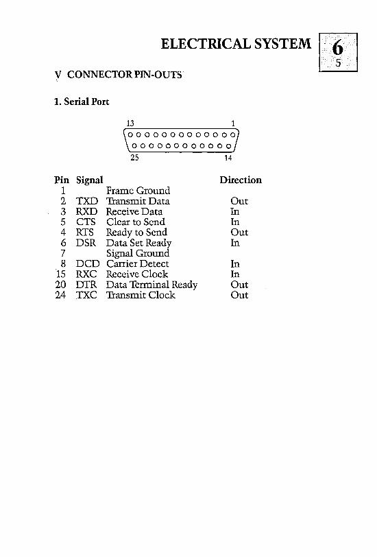
ELECTRICAL SYSTEM W v CONNECTOR PIN-OUTS'
1. Serial Port
Pin Signal 1 2 TXD 3 RXD 5 CTS 4 RTS 6 DSR 7 8 DCD
15 RXC 20 DTR 24 TXC
13 0000000000000
000000000000
25 14
Direction Frame Ground Transmit Data Out Receive Data In Clear to Send In Ready to Send Out Data Set Ready In Signal Ground Carrier Detect In Receive Clock In Data Terminal Ready Out Transmit Clock Out
I>~~I ELECTRICAL SYSTEM
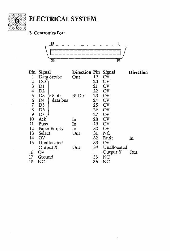
2. Centronics Port
18 1
\1 I) 36 19
Pin Signal Direction Pin Signal Direction 1 Data Strobe Out 19 OV 2 DO 20 OV 3 Dl .21 OV 4 D2 22 OV 5 D3 8 bit BiDir 23 OV 6 D4 data bus 24 OV 7 D5 25 OV 8 D6 26 OV 9 D7 27 OV
10 Ack In 28 OV 11 Busy In 29 OV 12 Paper Empty In 30 OV 13 Select Out 31 NC 14 OV 32 Fault In 15 Unallocated 33 OV
Output X Out 34 Unallocated 16 OV Output Y Out 17 Ground- 35 NC 18 NC 36 NC
ELECTRICAL SYSTEM
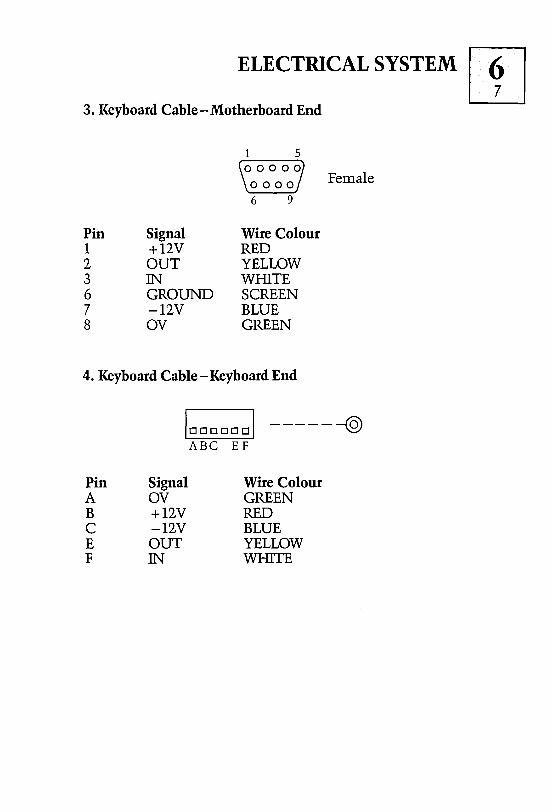
3. Keyboard Cable-Motherboard End
Pin 1 2 3 6 7 8
Signal +12V OUT IN GROUND -12V OV
5
Wire Colour RED YELLOW WI-llTE SCREEN BLUE GREEN
Female
4. Keyboard Cable - Keyboard End
Pin A B C E F
10000001 ------@ ABC EF
Signal OV +12V -12V OUT IN
Wire Colour GREEN RED BLUE YELLOW WI-llTE
II}~:I ELECTRICAL SYSTEM
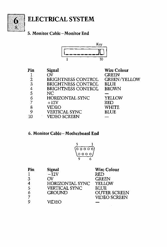
5. Monitor Cable - Monitor End
Pin 1 2 3 4 5 6 7 8 9
10
Signal OV BRIGHTNESS CONTROL BRIGHTNESS CONTROL BRIGHTNESS CONTROL NC HORIZONTAL SYNC +12V VIDEO VERTICAL SYNC VIDEO SCREEN
10
Wire Colour GREEN GREEN /YELLOW BLUE BROWN
YELLOW RED WHITE BLUE
6. Monitor Cable-Motherboard End
Pin 1 3 4 5 6 7 9
Signal -12V OV
5 1
HORIZONTAL SYNC VERTICAL SYNC GROUND
VIDEO
Wire Colour RED GREEN YELLOW BLUE OUTER SCREEN VIDEO SCREEN
ELECTRICAL SYSTEM
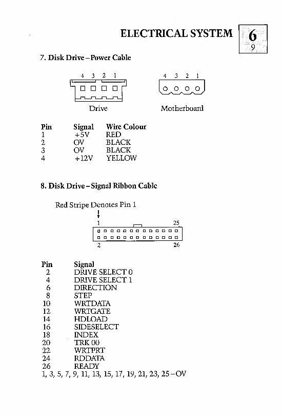
7. Disk Drive - Power Cable
Pin 1 2 3 4
432 1
~ Drive
Signal +5V OV OV +12V
Wire Colour RED BLACK BLACK YELLOW
8. Disk Drive - Signal Ribbon Cable
Red Stripe Denotes Pin 1
~ 1
4 3 2 1
~ Motherboard
25 o 0 000 0 0 0 0 0 0 0 0
o c c c c c ceo 0 0 0 C
2 26
Pin Signal 2 DRIVE SELECT 0 4 DRIVE SELECT 1 6 DIRECTION 8 STEP
10 WRTDATA 12 WRTGATE 14 HDLOAD 16 SIDES ELECT 18 INDEX 20 TRKOO 22 WRTPRT 24 RDDATA 26 READY 1,3,5,7,9, II, 13, 15,17,19,21,23, 25-0V
Ifbgil ELECTRICAL SYSTEM
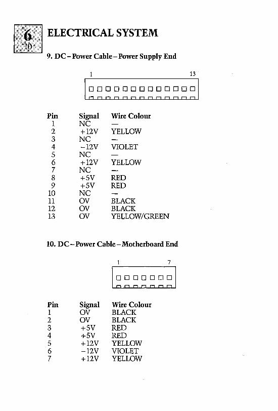
9. DC - Power Cable - Power Supply End
1 13
I~~~~~~~~~~~~~I Pin Signal Wire Colour
1 NC 2 +12V YELLOW 3 NC 4 -12V VIOLET 5 NC 6 +12V YELLOW 7 NC 8 +5V RED 9 +5V RED
10 NC 11 OV BLACK 12 OV BLACK 13 OV YELLOW/GREEN
10. DC - Power Cable - Motherboard End
Pin 1 2 3 4 5 6 7
Signal OV OV +5V +5V +12V -12V +12V
1 7
I~~~~~~~I Wire Colour BLACK BLACK RED RED YELLOW VIOLET YELLOW
ELECTRICAL SYSTEM m LiU
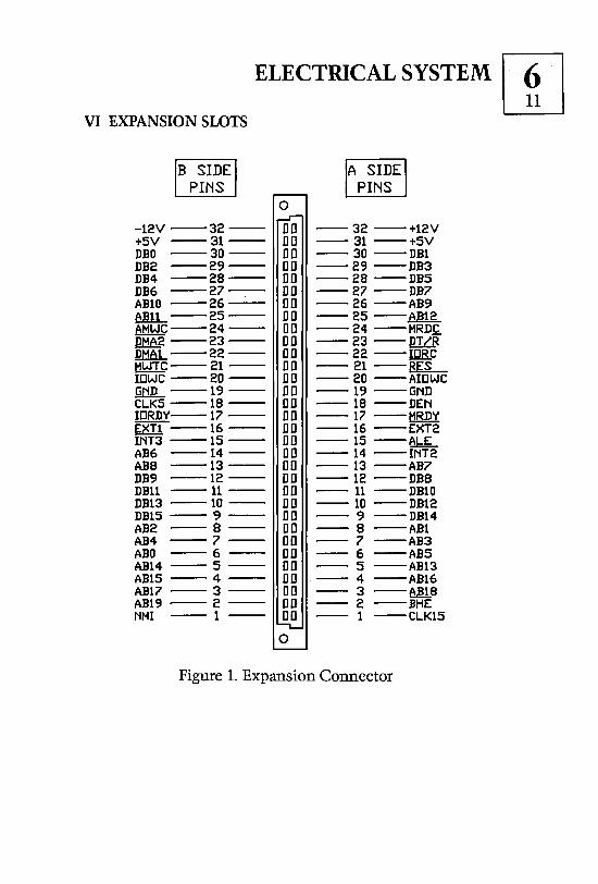
VI EXPANSION SLOTS
o -12V --32 -- DO +5V --31-- DO DBO --30 -- DO DB2 --29 -- DO DB4 --28 -- DO DB6 --27 -- DO ABIO --26 -- DO tWL--25-- DO AMWC--24 -- DD DMA2 --23 -- DO DMA1 --22 -- DO MWTC-- 21 -- DO IOWC --20 -- DO Yt!1L --19 -- DO ClK5 --18 -- DO IORDY--17 -- DO EXT1 --16 -- DO INT3 --15 -- DO AB6 --14 -- DO ABa --13 -- DO DB9 --12 -- DO DB11 --11 -- DO DB13 -- 10 -- DO DBIS -- 9 -- DO AB2 -- a -- DD AB4 --7 -- DD ABO -- 6 -- DD AB14 -- 5 .-- DD AB15 -- 4 -- DD AB17 -- 3 -- DO AB19 -- 2 -- DD NMI -- 1 -- DD
o
--32 --+12V --31 --+SV --30 --DBl --29 --DB3 --28 --DBS --27 --DB7 --26 --AB9 --25--~ --24 --MRDC --23 --DT/R -- 22 --lQB..C --21--~ -- 20 --AIDWC --19 --GND --18 --DEN -- 17 -- t1BID: --16 --EXT2 --15--~ --14 --INT2 --13 --AB7 --12 --DBa -- 11 --DBI0 --10 --DB12 -- <3 --DBl4 -- 8 --ABI -- 7 --AB3 -- 6 --ABS -- 5 --AB13 -- 4 --ABl6 -- 3 --e.m..a -- 2 --BHE -- 1 --ClKlS
Figure 1. Expansion Connector
I>grl ELECTRICAL SYSTEM
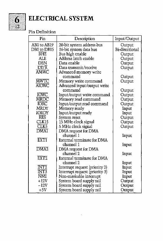
Pin Definition
Pin Description Input/Output
ABO toABl9 20-bit system address bus Output DBOtoDBlS l6-bit system data bus Bi-directional
BHE Bus high enable Output ALE Address latch enable Output DEN Data enable Output DT/R Data transmit/receive Output
AMWC Advanced memory write command Output
MWTC Memory write command Output AIOWC Advanced input/output write
command Output IOWC Input/output write command Output MRDC Memory read command Output IORC Input/output read command Output
MRDY Memory ready Input IORDY Input/output ready Input
RES System reset Output CLKIS 15 MHz clock signal Output CLKS 5 MHz clock signal Output DMAI DMA request for DMA
channell Input EXTl External terminate for DMA
channell Input DMA2 DMA request for DMA
channel 2 Input EXT2 External terminate for DMA
channel 2 Input INT2 Interrupt request (priority 2) Input INT3 Interrupt request (priority 3) Input NMI Non-maskable interrupt Input +l2V System board supply rail Output -l2V System board supply rail Output +SV System board supply rail Output
ELECTRICAL SYSTEM m ~
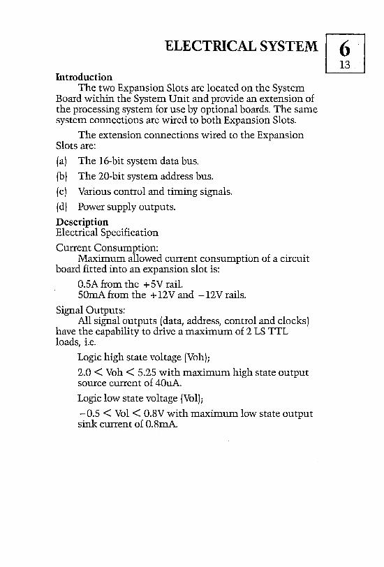
Introduction The two Expansion Slots are located on the System
Board within the System Unit and provide an extension of the processing system for use by optional boards. The same system connections are wired to both Expansion Slots.
The extension connections wired to the Expansion Slots are:
(a) The 16-bit system data bus.
(b) The 20-bit system address bus.
(c) Various control and timing signals.
(d) Power supply outputs.
Description Electrical Specification
Current Consumption: Maximum allowed current consumption of a circuit
board fitted into an expansion slot is:
O.SA from the + SV rail. SOmA from the + 12V and -12V rails.
Signal Outputs: All signal outputs (data, address, control and clocks)
have the capability to drive a maximum of 2 LS TTL loads, i.e.
Logic high state voltage (Voh);
2.0 < Voh < 5.25 with maximum high state output source current of 40uA.
Logic low state voltage (Vol);
-0.5 < Vol < 0.8V with maximum low state output sink current of 0.8mA.

1':;61
ELECTRICAL SYSTEM w
e J4:< Expansion Slots Signal Inputs:
The signal inputs to the data bus require a tri-state driver stage meeting the following requirements.
Logic high state voltage (Voh);
2.4 < Voh < S.2SV with maximum high state output source current of 400uA.
Logic low state voltage (Vol);
-0.5 < Vol < O.SV with maximum low output state sink current of 8mA.
All the remaining inputs are control inputs and require to be driven by an open collector driver stage. The input control lines on the System Board are fitted with pull-up resistors (3.3k).
Pin Detail Both Expansion Slots are 64-way connectors
(DIN 41612, 2 by 32 female, with a type B housing) and are identical with regard to the connections to the system buses, as illustrated on the diagram of an Expansion Connector on page 6-11.
ELECTRICAL SYSTEM
l-a 147.0 ~I
T 0 0
I MAIN PCB
a COMPONENT SIDE ci
'"
I DIN 41612 TYPE B 64 PIN
1 ~ 0 0
T - - - -- - MAX. COMPONENT HEIGHT
x K • 2D "" fOR EXP SLOT 2 X & lS ,.,. r~ E.XP SLOT 1
(::::~:::::::::::::::::::::::::::J
DIMENSIONS. ALL SIZES ARE IN MILLlMETRES UNLESS If) OTHERWISE SPECIF'IED cD TOLERANCES, BOARD SIZE, -+1- 0.2
1-~==j4i-r--_1_0._6 __________ 0_TH_E_R_S_, _-+_1-_0_.1_____________ 3.5
'\ BOARD AREA NOT AVAILABLE
3 HOLES 3.BSMM DIA. AFTER THROUGH HOLE PLATING
MAIN PCB COMPONENT SIDE
COMPONENT CLEARANCE 6.5MM DIA.
64 HOLES ON 0.1' PITCH COMPONENT CLEARANCE 6.5MM DIA.
1.lMM DIA. AFTER ~ THROUGH HOLE PLATING /
32 1 ooooooooooooooooooooooooooooooooB ooooooooooooooooooooooooooooooooA
o 0 ----.-------~-----~
2 HOLES 2.BMM DIA. 2.50 ...,
AFTER THROUGH HOLE PLATING 7.58"" 10.12...,
14 --86.32'--------.t ~-------------91.40-------i~
14-------------140.50 ------------.,
FIG. 2. EXPANSION BOARD DETAIL
[IJ
1\/6<1 ELECTRICAL SYSTEM
·~i6 • vn DIRECT ASYNC CONNECTION CABLE
HOST APRICOT Connector 'N. MaleDB-25
Pin
Connector 'B' MaleDB-25
Pin 1 ____ _ 1 2 ____ _ 3 3 ____ _ 2 4 ____ _ Wired
IBM Connector 'B'
Female 25 Pin
1 3 2
~J together [~ Wired [58----
together 6 ____ _ 7 ____ _
20 ____ _
Modem Connection Cable
4
20 7 6
APRICOT Connector 'N. MaleDB-25
HOST Connector 'B' Male DB-25
Pin 1 ____ _ 2 ____ _ 3 ____ _ 4 ____ _ 5 ____ _ 6 ____ _ 7 ____ _ 8 ____ _
20 ____ _
Pin
1 2 3 4 5 6 7 8
20
4
20 7 6

ELECTRICAL SYSTEM m LEJ vm PRINTERS
The ACT Apricot will drive most printers currently on the market, with either Centronics compatible or RS232 in terfaces.
Parallel All ACT printers currently marketed, are of the
parallel type, and will work with the Apricot, as long as the interface cable supplied with the printer is used.
The Apricot defaults to the parallel port on switch on, and no re-configuring of the operating system is required.
Below is given the wiring of the standard cable:
Pin No. Signal 1 Strobe 2 Data 0 3 Data 1 4 Data 2 5 Data 3 6 Data 4 7 Data 5 8 Data 6 9 Data 7
11 Busy 16 OV 17 Ground
ri!,~1 ELECTRICAL SYSTEM
In order to utilise the additional facilities built into the Apricot BIOS i.e. Fault, Select, Paper Empty, a new cable will be required, as below:
Pin No. Signal Pin No. 1 Strobe 9 2 Data 0 11 3 Data 1 12 4 Data 2 13 5 Data 3 16 6 Data 4 17 7 Data 5 32 8 Data 6 33
Serial
Signal Data 7 Busy Paper Empty Select OV Ground Fault Ground
Serial printers are also supported by the Apricot via the RS232 port, but certain things need to be done for correct operation.
1. Use a cable as specified by the printer manufacturer. Below is given a suggested wiring, but is by no means correct for every printer, and is only given as a possible starting point:
Apricot Printer 1 ____ 1 2 ____ 3 7 ____ 7 5 ____ 20
Signal
Screen Data
Ground Busy
2. Re-configure the system to allow printing via the serial port. Use baud rates, number of stop bits, parity etc., as suggested by the printer manufacturer.
3. Change the switch settings, built into all serial printers, to match the parameters of the now changed system.
4. Certain printers use Pin 11 or 19 as 'Busy' or CTS~ Refer to the printers handbook for correct pin.
If any problems are encountered, consult either your dealer or printer manufacturer.

I L..-_E_L_E_C_T_RO_N_I_C_S_Y_ST_E_M __ ---'·I~ I Outline of System
IT Integrated Circuit Catalogue
III Mnemonics
IV Memory Map
V Ram Expansion Card Details
VI Modem Card Details

ELECTRONIC SYSTEM W This section of the manual is devoted to a brief outline
of the Apricot electrical/electronic system. It is not intended to be an in-depth study, but an overview using block diagrams. For a more detailed insight into the circuit~ refer to the Apricot Technical Reference Manual.
In addition to block diagrams, section II is a catalogue of all the integrated circuits, their truth tables and functions within the machine.
Appendix E contains a complete circuit diagram of the motherboard.
t~i? .... 1 ELECTRONIC SYSTEM
I OUTLINE OF THE SYSTEM
The ACT Apricot can be broken down into 5 sections -the display, memory, multiprocessor structure, I/O section and disk drive.
The monitor and keyboard will also be briefly described.
1. The Display
In essence the display consists of 4 parts - the CRT controller, static ram, dynamic ram and finally the video section.
All sections are configured in a "pipeline" structure, in that the output of one section forms the basic input to the next.
The CRT controller generates in addition to vertical and horizontal sync pulses, memory addresses MAO-MAIO.
These addresses are sequentially generated and are the memory address lines for the static screen ram. As the screen consists of 80 characters by 25 lines, the static ram requires 2000 locations (80 x 25). Each character requires 2 bytes and hence the screen memory is a 4K x 8 configuration.
The screen is accessed sequentially line by line, starting at the top left hand character position - this is location FOOO:OH in the memory map.
FOOO:O
FIOO:O Screen Ram
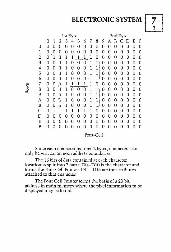
ELECTRONIC SYSTEM W I 1st Byte 2nd Byte I o 1 234 S 6 7 8 9 ABC D E F
00000000000000000 10000000000000000 2 0 ~.L 1 1 _l.._.J __ L. 1 0 0 0 0 0 0 0 0 3 0 0 1 1 0 0 0 1 l' 0 0 0 0 0 0 0 400110001110000000 S 001100011 1 0000000 6 0 0 1 1 0 0 0 '1 1J 0 0 0 0 0 0 0 7 0 0 11 1 J ___ L_!. __ 1 0 0 0 0 0 0 0 0 80011000110000000 9 0 01 1 0 0 0 1 1 0 0 0 0 0 0 0 A 0 0 11 1 0 0 0 11 1 0 0 0 0 0 0 0 BOO ·1 1 0 0 0 : 1 L 0 0 0 0 0 0 0 C O~" 1'-' 1 1 1 or' 1" L' 0 0 0 0 0 0 0 0 L,_. __________ .~ __
D 0000000000000000 E 0000000000000000 F 0 0 000 0 0 0 0 0 0 0 0 0 0 0
Font-Cell
Since each character requires 2 bytes, characters can only be written on even address boundaries.
The 16 bits of data contained at each character location is split into 2 parts: DO - D10 is the character and forms the Font Cell Pointer, D11-DIS are the attributes attached to that character.
The Font Cell Pointer forms the basis of a 20 bit address in main memory where the pixel information to be displayed may be found.
ErJ ELECTRONIC SYSTEM
Font-Cell Pointer Rows
Address
0 0 0 0 0 0 0 1 10 0 1 0 1 10 a 010 a a 01 1st Byte-Row a
a 0 0 0 a a 0 1 10 a a 11 0 a 0 0 a a 1 I 2nd Byte-Row a
a 0 a 0 0 0 01 0 a 01 0 0 0 0 a I 1st Byte - Row 1
a 0 0 0 a a 0 1 10 a 0 1 10 a 0 0 a 1 I 2nd Byte-Row 1
a a a a a a 01 0 a 010 a a a 0 I 1st Byte-Row 2
a a a a a a a 1 10 a 1110 11 0 10 10 all a 11 I 2nd Byte-Row 2
First 6 Addresses of One Character
The CRT controller generates 4 additional signals: RAO - RA3. These are the row addresses. There are 16 rows of pixels for each character and hence we access 32 contiguous memory locations.
The remaining address bits are made up as follows:
A16, A17, A18, A19 all are o since the fonts must be within the lower 64K of the lower 128K.
In character mode the first 10 pixels are displayable, the remaining 6 being OJ except the 2 high order bits which may be programmed for underline or strike through. In graphics mode all 16 are displayable.
The 10 or 16 bits, dependant on mode, are parallel loaded into 2 shift registers (IC69, 87) and are clocked out under the control of CLK1S and LES. The resultant serial stream is the raw video signal to be combined with the attributes previously "stripped off" from the screen ram and formed into the final video signal. Together with the horizontal and vertical sync pulses a direct drive set of signals is passed to the monitor.
2. The Memory
ELECTRONIC SYSTEM W The ACT Apricot has, as standard, 2S 6K of
onboard memory implemented with 32 64K x 1 dynamic RAM chips type 3764-20. These are arranged as two banks of 64K x 16, designatedMAO-MA1S. Data may be accessed 16 bits at a time but high and low order bytes may be written independantly.
The memory is dual-ported and memory access cycles occur on request for CPU cycles and continuously for video and refresh cycles. The state of the CCLK square wave determines the type of cycle performed, continuous RAS and CAS signals are generated by lC36.
The address source for the DRAMs is chosen from the following:
CPU (a) lC61 and 63 allow CPU to address the memory, in conjunction with AB17 which routes the RAS and CAS signals to the A or B 64K memory block.
SCREEN (b) lCSS and 60 allow the screen RAM output data to address the lower 64K bytes of memory bank A.
REFRESH (c) Refresh addresses are supplied instead of screen RAM data during display blanking intervals. These are supplied by the 8 bit binary counter (lC37) and its associated buffer (lC48). Row addresses are enabled onto the DRAM address bus by lCSS or lC61, or lC48 as selected by the cycle type, i.e. screen, CPU or refresh respectively. These are strobed into the DRAMS by the negative going edge of RAS and after a typical 30ns delay generated by the invertors within lC47 the column address is gated onto the address bus before CAS occurs.
The initial boot software, diagnostics and calculator are contained in 2 x 64K eproms (ICS3 and S9) enabled by signal NCSP at memory locationFCOOOH.
[[.;;~;j~1 ELECTRONIC SYSTEM
3. The Multiprocessor Structure
8086 The ACT Apricot utilizes the 8086
microprocessor running at 5 MHz, making it a true 16 bit microcomputer. In conjunction with the main processor, an 8089 I/O co-processor is included as standard, together with an optional 8087 numeric data processor.
8089 The 8089 takes a substantial software overhead
off the 8086 during disk operations and permits concurrent communications processing.
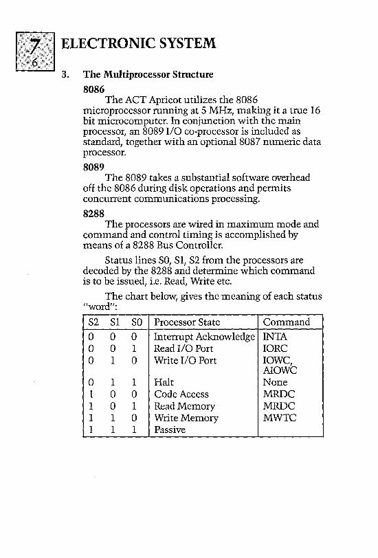
8288 The processors are wired in maximum mode and
command and control timing is accomplished by means of a 8288 Bus Controller.
Status lines SO, Sl, S2 from the processors are decoded by the 8288 and determine which command is to be issued, i.e. Read, Write etc.
The chart below, gives the meaning of each status "word":
S2 Sl SO Processor State Command
a a a Interrupt Acknowledge INTA a a 1 Read I/O Port 10RC a 1 a Write I/O Port 10WC,
AIOWC a 1 1 Halt None 1 a a Code Access MRDC 1 a 1 Read Memory MRDC 1 1 a Write Memory MWTC 1 1 1 Passive
ELECTRONIC SYSTEM
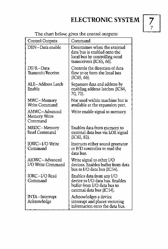
The chart below, gives the control outputs:
Control Outputs Command DEN - Data enable Determines when the external
data bus is enabled onto the local bus by controlling octal transceivers (IC65, 66).
DT/R-Data Controls the direction of data Transmit/Receive flow to or from the local bus
(IC65, 66).
ALE - Address Latch Separates data and address by Enable enabling address latches (IC64,
70,72). MWC-Memory Not used within machine but is Write Command available at the expansion port.
AMWC - Advanced Write enable signal to memory. Memory Write Command
MRDC-Memory Enables data from memory to Read Command external data bus via LOE signal
(IC62, 82).
10WC - I/O Write Instructs either sound generator Command or F/D controller to read the
data bus.
AIOWC - Advanced Write signal to other I/O I/O Write Command devices. Enables buffer from data
bus to I/O data bus (IC54).
10RC - I/O Read Enables data from any I/O Command device to I/O data bus. Enables
buffer from I/O data bus to external data bus (IC 54).
INTA - Interrupt Acknowledges a device Acknowledge interrupt and places vectoring
information onto the data bus.
lii:~1 ELECTRONIC SYSTEM
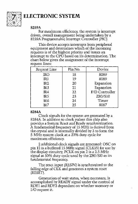
8259A For maximum efficiency, the system is interrupt
driven, overall management being undertaken by a 82S9A Programmable Interrupt Controller (PIC).
This device accepts interrupts from peripheral equipment and determines which of the incoming requests is of the highest priority and issues an interrupt to the CPU based on its determination. The chart below gives the assignment of the interrupt request lines:
Request Line Pin No. Device
IRO 18 8089 IRI 19 8089 IR2 20 Expansion IR3 21 Expansion IR4 22 FID Controller IRS 23 Z80/S10 IR6 24 Timer IR7 25 8087
8284A Clock signals for the system are generated by a
8284A. In addition to clock pulses this chip also provides a System Reset and Ready synchronization. A fundamental frequency of 15 MHz is derived from the crystal and is internally divided by 3 to form the 5 MHz system clock at a 33% duty cycle for maximum efficiency.
2 additional clock signals are generated: OSC on pin 12 is a buffered 15 MHz signal (CLKlS) for use by the display circuitry, PCLK on pin 2 is a 2.5 MHz signal at 50% duty cycle used by the Z80/SIO as its fundamental frequency.
The reset input (RESIN) is synchronized to the falling edge of CLK and generates a system reset (RESET).
Generation of wait states, when necessary, is accomplished by READY signal under the control of RDYI and RDY2 dependant on whether memory or 1/0 request it.
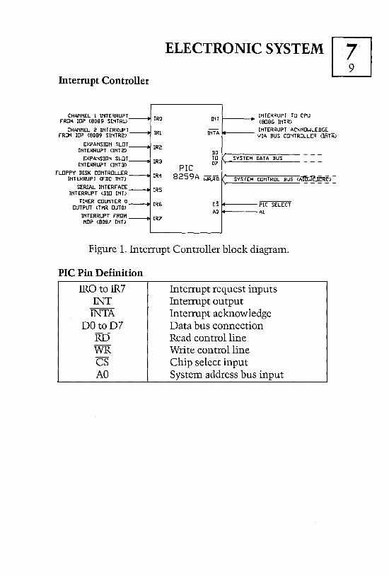
Interrupt Controller
ELECTRONIC SYSTEM W CHANNEL 1 INTERRUPT IRO INT
INTERRUPT TO CPU FROM lOP <8089 SINTR1) (8086 INTR)
CHANNEL 2 INTERRUPT lRl INTA INTERRUPT ACKNOWLEDGE
FROM lOP (8089 SINTR2) VIA BUS CONTROLLER <INT A)
EXPANSION SLOT 1R2 INTERRUPT (INT2) DO EXPANSION SLOT 1R3
TO SYSTEM DATA BUS INTERRUPT (INT3) PIC
D7
FLOPPY DISK CONTROLLER INTERRUPT <FDC INT>
1R4 8259A WR,RD SYSTEM CONTROL BUS (AiE~.~) = SERIAL INTERFACE
IRS INTERRUPT <SIO INT>
TIMER COUNTER 0 IR6 B PIC SELECT OUTPlJT <TMR OUTO) AO A1
INTERRUPT FRDM IR7 NDP (8087 INT>
Figure 1. Interrupt Controller block diagram.
PIC Pin Definition
IRO to IR7 INT
INTA DO to D7
RD WR CS AO
Interrupt request inputs Interrupt output Interrupt acknowledge Data bus connection Read control line Write control line Chip select input System address bus input

[[] ELECTRONIC SYSTEM
4. The I/O Section
(a) Sound Generator The sound generator consists of a SN764B9
together with an associated octal latch and clock circuitry.
The SN764B9 contains 3 programmable tone generators, a noise generator, attenuation registers and an audio output stage. It is memory mapped at location SOH and enabled by signals CSC or IW. Data is latched from the I/O bus via an octal latch (ICIB), under the control of the same signals. When data is latched in, it raises WE (Pin S) to confirm the data is in. The SN764B9 uses a fundamental frequency of 2 MHz derived from a 4 MHz crystal oscillator module (ICBI) divided by 2 (ICBI).
A TBAB20 (ICB) is used for the audio output stage. There is also an auxilIary input to this amplifier, for reproduction of sound via the internal speaker.
For a detailed description of this interface, refer to the Apricot Technical Reference Manual.
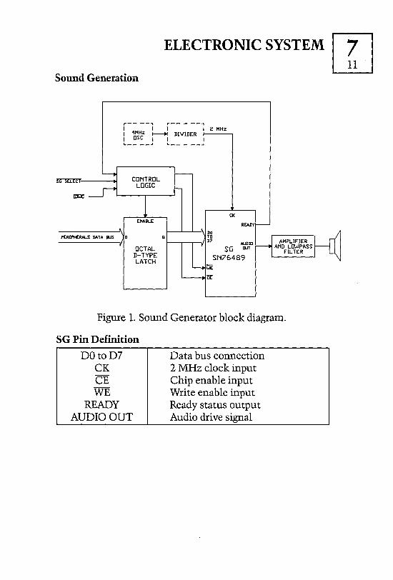
ELECTRONIC SYSTEM m li!J
Sound Generation
,..-- --, ,..-- - --., : 4MHz :-.l DIVIDER I 2 MHz I OSC I I I L ____ .J L _____ .J
ptRIPt£RALS DATA IUS D
OCTAL D-TYPE LATCH
1--......... -'---'\ I DO Q TO
I---.,....--;r-"V I D7
CK
R[ADY
AUDIO SG [JJT
SN76489
Figure 1. Sound Generator block diagram.
SG Pin Definition
DO to D7 CK CE WE
READY AUDIO OUT
Data bus connection 2 MHz clock input Chip enable input Write enable input Ready status output Audio drive signal
lo!~~~~(1 ELECTRONIC SYSTEM
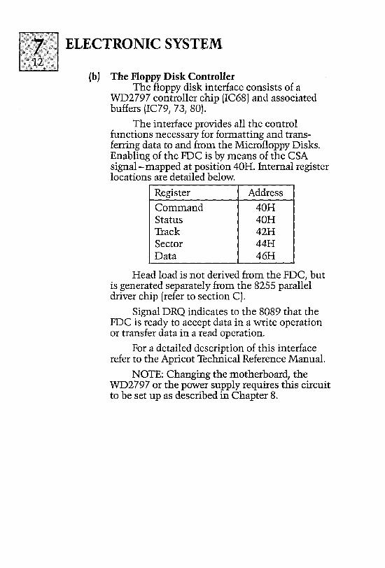
(b J The Floppy Disk Controller The floppy disk interface consists of a
WD2797 controller chip (IC68) and associated buffers (IC79, 73, 80).
The interface provides all the control functions necessary for formatting and transferring data to and from the Microfloppy Disks. Enabling of the FDC is by means of the CSA signal-mapped at position 40H. Internal register locations are detailed below.
Register Address
Command 40H Status 40H Track 42H Sector 44H Data 46H
Head load is not derived from the FDC, but is generated separately from the 8255 parallel driver chip (refer to section C).
Signal DRQ indicates to the 8089 that the FDC is ready to accept data in a write operation or transfer data in a read operation.
For a detailed description of this interface refer to the Apricot Technical Reference Manual.
NOTE: Changing the motherboard, the WD2797 or the power supply requires this circuit to be set up as described in Chapter 8.
ELECTRONIC SYSTEM m LiU
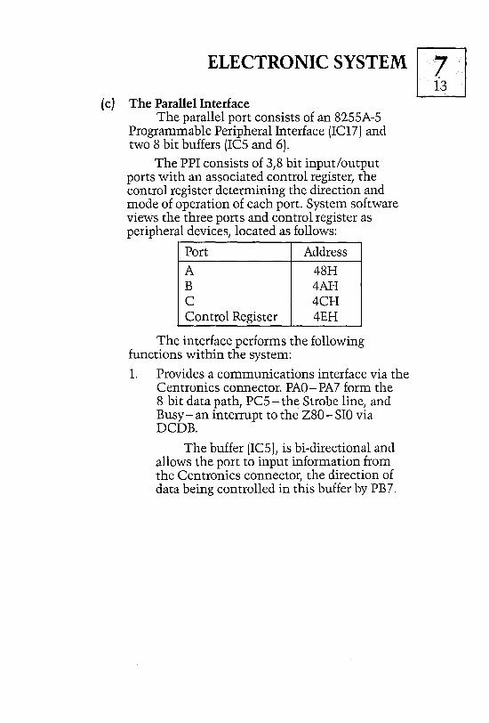
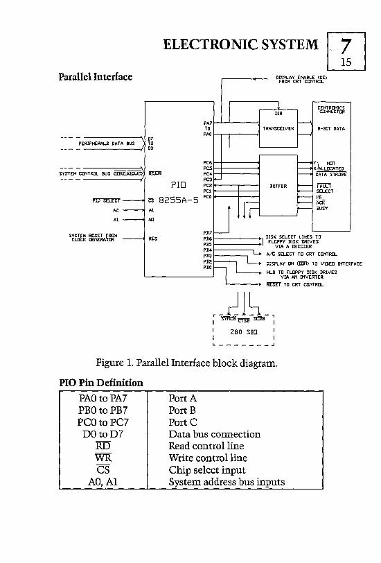
(cJ The Parallel Interface The parallel port consists of an 82SSA-S
Programmable Peripheral Interface (ICI?) and two 8 bit buffers (ICS and 6).
The PPI consists of 3,8 bit input/output ports with an associated control register, the control register determining the direction and mode of operation of each port. System software views the three ports and control register as peripheral devices, located as follows:
Port Address
A 48H B 4AH C 4CH Control Register 4EH
The interface performs the following functions within the system:
1. Provides a communications interface via the Centronics connector. PAO-PA? form the 8 bit data path, PCS - the Strobe line, and Busy-an interrupt to the Z80-SIO via DCDB.
The buffer (ICS), is bi-directional and allows the port to input information from the Centronics connector, the direction of data being controlled in this buffer by PB?
Izl ELECTRONIC SYSTEM
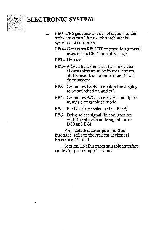
2. PBO-PB6 generate a series of signals under software control for use throughout the system and comprise:
PBO - Generates RESCRT to provide a general reset to the CRT controller chip.
PBl- Unused.
PB2 - A head load signal HLD. This signal allows software to be in total control of the head load for an efficient two drive system.
PB3 - Generates DON to enable the display to be switched on and off.
PB4 - Generates AIG to select either alphanumeric or graphics mode.
PBS - Enables drive select gates (IC79).
PB6- Drive select signal. In conjunction with the above enable signal forms DSO andDS1.
For a detailed description of this interface, refer to the Apricot Technical Reference Manual.
Section 1.5 illustrates suitable interface cables for printer applications.
Parallel htterface
------..... ID7 PERIPHERALS DATA BUS TO ______ -11 DO
ELECTRONIC SYSTEM m ~
PA71--'--L.---4,1
DISPLAV ENAIILE (DE> fROM CRT CONTROL.
CENTRONICS ClJNNE:CTOR
TO TRANSCEIVER PAD i--r----r---II
PC6 f---+-----ti PC!5~-----tI
SYSTEM CONTROL. BUS UDRc.A""ffiWc> 1m.t:JR PC4i-+----oi PC3
PID PC2io-----r---i BUffER PCl I----+----i
~ ts 8255A-5 PCD
fAULT SEL.ECT PE ACK BUSY A2 Al
Al All
SYSTEM RESET FROM CLOCK GENERATOR RES
PB7
PpBBS61-------) D~~M~~~IK LMieE1° VIA A DECODER
~!~ Ale SELECT TO CRT CONTROL.
PB2 DISPl.AV ON rnm> TO VIDEO INTERfACE PIO
HLD TO F"L.OPPY DISK DRIVES VIA AN INVERTER
RnET TO CRT CONTROL.
._~l~L, 1 -rmc:J" ~ llt:ll»' 1
280 SID L _______ J
Figure 1. Parallel Interface block diagram.
PIO Pin Definition
PAO to PAl PBO to PB? PCOto PC?
DO toD? RD WR CS
AO,AI
PortA PortB PortC Data bus connection Read control line Write control line Chip select input System address bus inputs
I~~{i:l ELECTRONIC SYSTEM
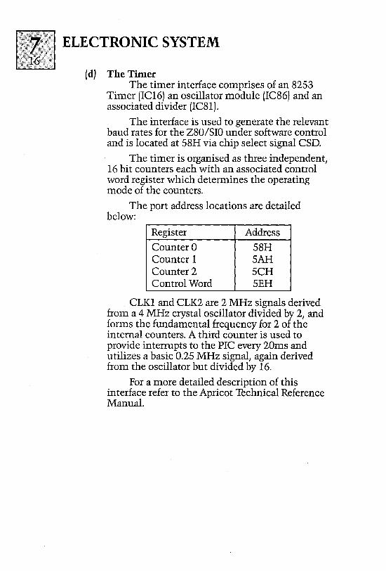
(dJ The Timer The timer interface comprises of an 8253
Timer (IC16) an oscillator module (IC86) and an associated divider (IC81).
The interface is used to generate the relevant baud rates for the Z80/SIO under software control and is located at 58H via chip select signal CSD.
The timer is organised as three independent, 16 bit counters each with an associated control word register which determines the operating mode of the counters.
The port address locations are detailed below:
Register Address Counter 0 58H Counter 1 5AH Counter 2 5CH Control Word 5EH
CLK1 and CLK2 are 2 MHz signals derived from a 4 MHz crystal oscillator divided by 2, and forms the fundamental frequency for 2 of the internal counters. A third counter is used to provide interrupts to the PIC every 20ms and utilizes a basic 0.25 MHz signal, again derived from the oscillator but divided by 16.
For a more detailed description of this interface refer to the Apricot Technical Reference Manual.
ELECTRONIC SYSTEM m LEJ
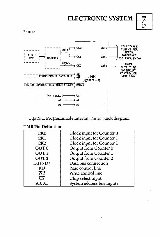
Timer
,. ____ ., ,. - - - - ~ 2MHz
I 4 MHz I I I
I DSC ~ DIVIDER I I I
CK2 DUT2
CKl DUTl J
SELECTABLE CLOCKS FOR
SERIAL INTERFACE
(SID TXCA/RXCA)
IO.25MHz CKO DUTO
= = = = = ~E~l-PH-E-RA-L-S-D-AT-A-B-U-S--\I ~8 TMR D7 8253-5
~Y~T~~ 9J~T~DL-B-U-S ..-,(I .... DR-C ...... J'lfJ-W .... C)--\I RD.WR
TMR SELECT CS
A2 Ai
Ai AD
TIMER DlJTPUT TO INTERRUPT
CONTROLLER (PIC IR6)
Figure 1. Programmable Interval Timer block diagram.
TMR Pin Definition
CKO CKI CK2
OUT 0 OUT I OUT 2
DO to D7 RD WR CS
AO/AI
Clock input for Counter 0 Clock input for Counter I Clock input for Counter 2 Output from Counter 0 Output from Counter I Output from Counter 2 Data bus connection Read control line Write control line Chip select input System address bus inputs
rzl ELECTRONIC SYSTEM
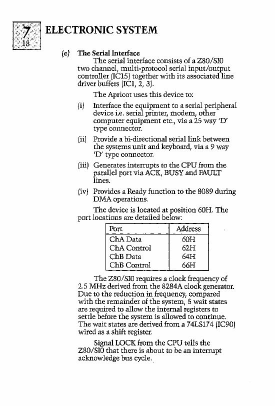
(e) The Serial Interface The serial interface consists of a Z80/SIO
two channel, multi-protocol serial input/output controller (ICI5) together with its associated line driver buffers (ICI, 2, 3).
The Apricot uses this device to:
(i) Interface the equipment to a serial peripheral device i.e. serial printer, modem, other computer equipment etc., via a 25 way 'D' type connector.
(ii) Provide a bi-directional serial link between the systems unit and keyboard, via a 9 way 'D' type connector.
(iii) Generates interrupts to the CPU from the parallel port via ACK, BUSY and FAULT lines.
(iv) Provides a Ready function to the 8089 during DMA operations.
The device is located at position 60H. The port locations are detailed below:
Port Address ChAData 60H ChAControl 62H ChB Data 64H ChB Control 66H
The Z80/SIO requires a clock frequency of 2.5 MHz derived from the 8284A clock generator. Due to the reduction in frequency, compared with the remainder of the system, 5 wait states are required to allow the internal registers to settle before the system is allowed to continue. The wait states are derived from a 7 4LSl7 4 (IC90) wired as a shift register.
Signal LOCK from the CPU tells the Z80/SIO that there is about to be an interrupt acknowledge bus cycle ..
ELECTRONIC SYSTEM m Li2J
1. ____ ..I SEUCT
r--, r---'~
I 4Mtz ~DIVlJ)£R DSC
1.--..1 1. ___ ..1
I PARALLEL : INTERF' ACE
DECODER LOcK F"R04 808618089
Siii"S£iTcT Aa
A1
TxJ)A I---~ LIN£ IbcIlA ~---I DRIVERI' iffiA RECEIVER iiTAAl----.I
SvncA 14---~ "ffiii ~---I iiCiiA ~---I
~ 1---. TO DRQZ rF lIP
Z80 S10/0
RXTXci
ma f'm' WI
DO TO D7
URQ
iii iii
ct !lA Clf
CLJ( R£UT
iffii iffiii
TdJ
RxJIJ
iiff
Figure 1. Serial Interface block diagram.
RS232C CONNECTOR !be a.Qa<
Tx a.oa<
Tx DATA
!be DATA
RTS
DTR
DSR
CTS Dell
KEYBOARD CONNECTOR
DATA IlIT
DATA lit
rtl~~"1 ELECTRONIC SYSTEM
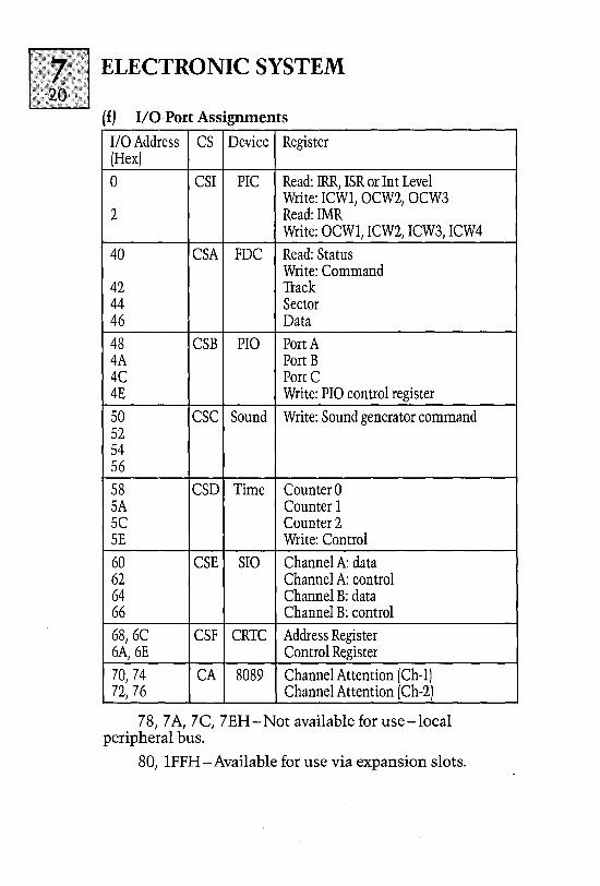
(fJ 1/0 Port Assignments
I/O Address CS Device Register (Hex)
0 CSI PIC Read: IRR, ISR or Int Level Write: ICWI, OCW2, OCW3
2 Read: IMR Write: OCWl, ICW2, ICW3, ICW4
40 CSA FDC Read: Status Write: Command
42 Track 44 Sector 46 Data
48 CSB PIO PortA 4A Port B 4C Port C 4E Write: PIO control register
50 CSC Sound Write: Sound generator command 52 54 56
58 CSD Time Counter 0 SA Counter 1 5C Counter 2 5E Write: Control
60 CSE SIO Channel A: data 62 Channel A: control 64 Channel B: data 66 Channel B: control
68,6C CSF CRTC Address Register 6A,6E Control Register
70, 74 CA 8089 Channel Attention (Ch-I) 72, 76 Channel Attention (Ch-2)
78, 7 A, 7C, 7EH-Not available for use-local peripheral bus.
80, IFFH - Available for use via expansion slots.
ELECTRONIC SYSTEM m UU
m ELECTRONIC SYSTEM
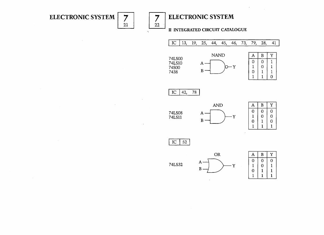
LEJ " n INTEGRATED CIRCUIT CATALOGUE
1 Ie 113, 19, 25, 44, 45, 46, 73, 79, 28, 41 1
NAND 74LSOO
74LS10 ABD-y 74S00 7438
A B Y
0 0 1 1 0 1 0 1 1 1 1 0
1 Ie 142, 78 1
AND A B Y
74LS08 AB----r-'Ly 74LS11 ~
0 0 0 1 0 0 0 1 0 1 1 1
1 Ie 1 52 I
OR A B Y
74LS32 zD-y 0 0 0 1 0 1 0 1 1 1 1 1
r- - - -l
I FUI'PV JllSI< I F1.tFPy JllSI< DRIVE DRIVE
I I L
-~Ir--' :..
SYSTEM BOARD ... ~
rUppy DISK ctJfTRa..1.£R
~ ~ ~ ~ .. ~
IU.. TlPRllCESSl/'tG A
ElEH£lfTS DATA JUS 1
~ I 8086 CPU I ADllR£SS JUS -I 8089 lOP I A - U
CIlfTRIl.. JUS
[~-~J .. - -
... ,... ... .". ... ~
PRtt4
r- - - -l
I PIWtT£R I I I L - ....... ~- .......J
... ~
PMf.L..lEL PRD1TER IIfTERfAct
.. :.. .. :.. .. j:..
~
~ ~ -
~~ --
... ~ ... ~ ... ~
2"K DRAM
c::::= c::::= c::::=
U r--
~ r--r-- -
D<PNlSIDrt SLOTS ( x2 )
DATA JUS I
AJlJlRESS JUS U
I r--
~~ r--COtTRtL. JUS
r--
DISPLAV CCtlTRILLER
APRICOT COMPUTER BLOCK DIAGRAM
DISPLAY ... UNIT
FIG. 1.2
ELECTRONIC SYSTEM I7l LkJ
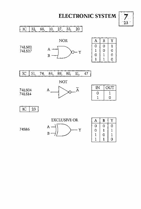
r-I I-c---'-13-2,-S-S,-10-,-27-,-3-3-, -2-0---'1
74LS02 74LS27
NOR
~=C>-y
1 IC I 51, 74, S4, S9, SO, II, 47 I NOT
74LS04 74LS14
1 IC 123 I
EXCLUSIVE OR
74S86 ~~D-Y
A B Y 0 0 1 1 0 0 0 1 0 1 1 0
1
m IOUTI o 1
1 0
A B y
0 0 0 0 1 1 1 0 1 1 1 0
r~il ELECTRONIC SYSTEM
I IC I 9, 21, 34, 35, 36 I 74LSl12 74S112
J-K FLIP-FLOP
SET
J Q
CLK ---1
K Q
Function Table
Inputs Outputs
Preset Clear Clock J K Q Q L H X X X H L H L X X X L H L L X X X H H H H t L L Q Q H H t H L H L H H ! L H L H H H ! H H IDGGLE H H H X X Q Q
IC9 Generates Write Enable to static rams when selected
via CSS.
Switches multiplexers (IC 38, 39, 40) to screen.
Provides 1 wait state when static ram is accessed via internal property of J:...-K flip-flop.
IC36 Generates RAS and CAS.
ELECTRONIC SYSTEM m ljU
IC35 Generates CCLK whose mark-space ratio depends on
whether alphanumerics or graphics.
Generates signals LES and LEC in antiphase, for enabling either processor or screen to drams.
IC34 Detects if there is enough time to do a processor
access to ram. If not, 1 wait state via RDY1 is inserted.
IC21 Generates Display Enable from CRT controller.
I IC 112,
74S74 74LS174
90
'D' TYPE FLIP - FLOP
SET
D Q
Q
CLEAR
Function Table
Inputs Outputs
Preset Clear Clock D Q Q
L H X X H L H L X X L H L L X X H H H H i L H L H H i H L H H H L X Q Q
ELECTRONIC SYSTEM
IC12 Provides 2 intensity levels under control of attributes.
IC90 Wired as a shift register and provides either 1 or 5 wait
states.
I Ie 118, 64, 70, 72, 62, 82
74LS373 ID' TYPE LATCHES
D Q
ENABLE OIP ENABLE
Function Table
Output Enable Outputs Control G D
L H H H L H L L L L X Q H X X Z
ELECTRONIC SYSTEM m li!J
IC18 Latches data from 1/0 data bus to sound generator via
signals 10WC and CSC.
IC64, 70, 72 Demultiplexes local addressldatabus and latches
address via signal ALE.
IC62,82 Enables data from drams to databus via signal LEC
and LOC.
I IC Iss, 60
74LS374 'D' TYPE LATCHES
D Q
CLK-----I
O/PENABLE
Function Table
Output CLOCKD Outputs Control
L i H H L i L L L L X Q H X X Z
Latches 16 bits of data from srams to be multiplexed onto drams address bus via signals CCLK and RAS.
liZ I ELECTRONIC SYSTEM
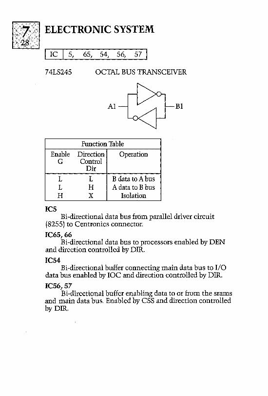
I IC I 5, 65, 54, 56, 57 I 74LS245 OCTAL BUS TRANSCEIVER
Al BI
Function Table
Enable Direction Operation G Control
Dir
L L B data to A bus L H A data to B bus H X Isolation
IC5 Bi-directional data bus from parallel driver circuit
(8255) to Centronics connector.
IC65, 66 Bi-directional data bus to processors enabled by DEN
and direction controlled by DIR.
IC54 Bi-directional buffer connecting main data bus to I/O
data bus enabled by 10C and direction controlled by DIR.
IC56,57 Bi-directional buffer enabling data to or from the srams
and main data bus. Enabled by CSS and direction controlled by DIR.
ELECTRONIC SYSTEM m Li2J
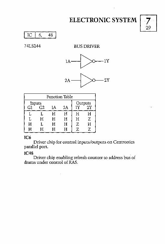
I IC I 6, 48
74LS244 BUS DRIVER
lA ---[:>r-lY 2A ---[:>r-2Y
Function Table
Inputs Outputs Gl G2 lA 2A lY 2Y L L H H H H L H H H H Z H L H H Z H H H H H Z Z
IC6 Driver chip for control inputs/outputs on Centronics
parallel port.
IC48 Driver chip enabling refresh counter to address bus of
drams under control of RAS.
IE)~;~}I ELECTRONIC SYSTEM
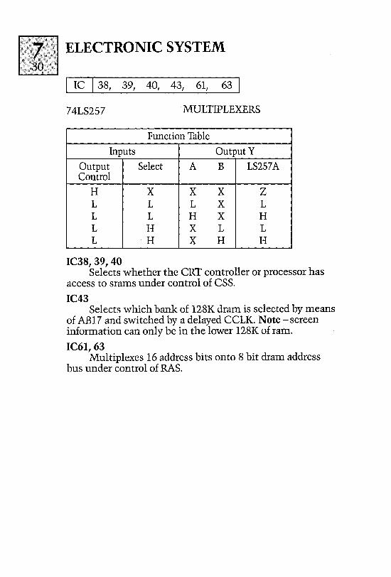
I IC I 38, 39, 40, 43, 61, 63
74LS257 MULTIPLEXERS
Function Table
Inputs Output Y
Output Select A B LS257A Control
H X X X Z L L L X L L L H X H L H X L L L H X H H
IC38, 39, 40 Selects whether the CRT controller or processor has
access to srams under control of CSS.
IC43 Selects which bank of 128K dram is selected by means
of AB17 and switched by a delayed CCLK. Note -screen information can only be in the lower 128K of ram.
IC61,63 Multiplexes 16 address bits onto 8 bit dram address
bus under control of RAS.
ELECTRONIC SYSTEM m Lid
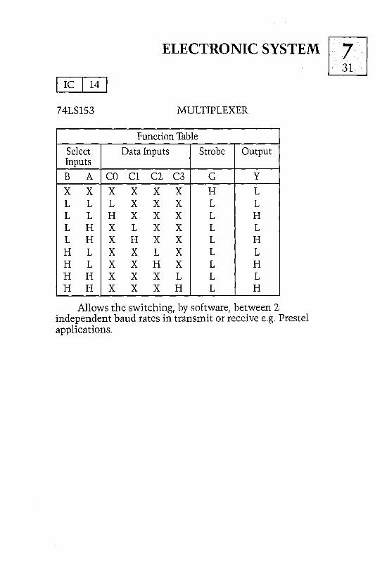
I Ie 114 74LS153 MULTIPLEXER
Function Table
Select Data Inputs Strobe Output Inputs
B A CO Cl C2 C3 G y
X X X X X X H L L L L X X X L L L L H X X X L H L H X L X X L L L H X H X X L H H L X X L X L L H L X X H X L H H H X X X L L L H H X X X H L H
Allows the switching, by software, between 2 independent baud rates in transmit or receive e.g. Prestel applications.
,. ~ 'ELECTRONIC SYSTEM
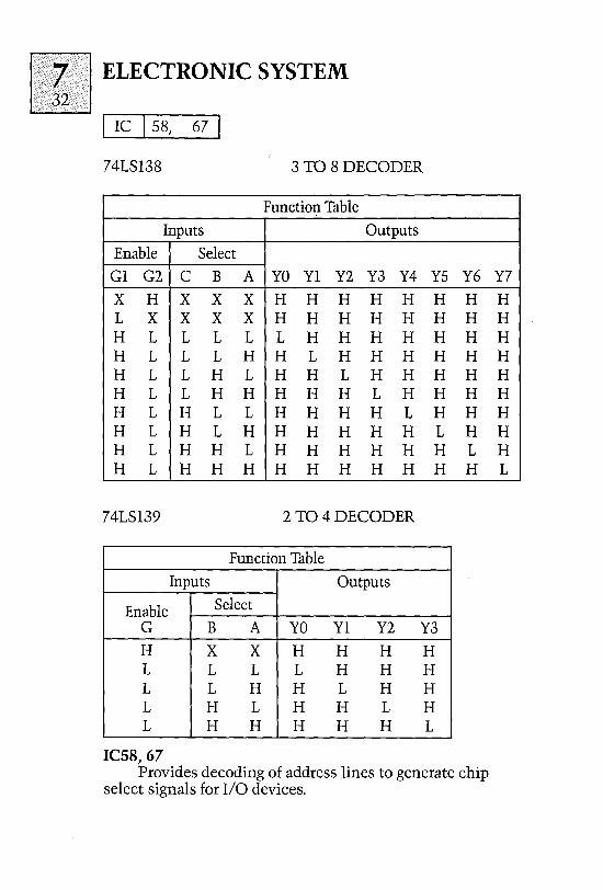
I IC 158, 67 I 74LS138 3 TO 8 DECODER
Function Table
Inputs Outputs
Enable Select
Gl G2 C B A YO Yl Y2 Y3 Y4 YS X H X X X H H H H H H L X X X X H H H H H H H L L L L L H H H H H H L L L H H L H H H H H L L H L H H L H H H H L L H H H H H L H H H L H L L H H H H L H H L H L H H H H H H L H L H H L H H H H H H H L H H H H H H H H H
74LS139 2 TO 4 DECODER
Function Table
Inputs Outputs
Enable Select
G B A YO Yl Y2 Y3 H X X H H H H L L L L H H H L L H H L H H L H L H H L H L H H H H H L
leS8,67
Y6 H H H H H H H H L H
Provides decoding of address lines to generate chip select signals for 1/0 devices.
Y7 H H H H H H H H H L
ELECTRONIC SYSTEM m LiU
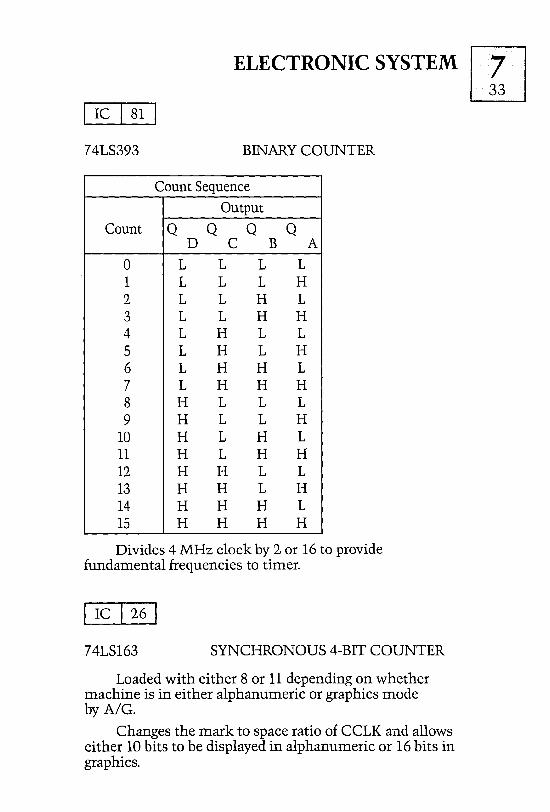
I IC I 81 I 74LS393 BINARY COUNTER
Count Sequence
Output
Count Q Q Q Q D C B A
0 L L L L 1 L L L H 2 L L H L 3 L L H H 4 L H L L 5 L H L H 6 L H H L 7 L H H H 8 H L L L 9 H L L H
10 H L H L 11 H L H H 12 H H L L 13 H H L H 14 H H H L 15 H H H H
Divides 4 MHz clock by 2 or 16 to provide fundamental frequencies to timer.
I IC 126 I 74LS163 SYNCHRONOUS 4-BIT COUNTER
Loaded with either 8 or 11 depending on whether machine is in either alphanumeric or graphics mode by A/G.
Changes the mark to space ratio of CCLK and allows either 10 bits to be displayed in alphanumeric or 16 bits in graphics.
I.'.~: •.•. :.:.;.;:i.';~.~.:.: .•.• :; .. ;.: ..... :.1.;1 ELECTRO NI C SYSTEM '·':·:}34::·>···,
j ,J , :"" " ~ ;' ~
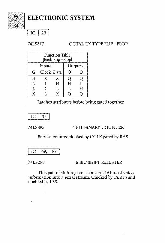
I IC 129 I 74LS377 OCTAL 'D' TYPE FLIP-FLOP
Function Table (Each Flip-Flop)
Inputs Outputs
G Clock Data Q Q
H X X Q Q L i H H L L i L L H X L X Q Q
Latches attributes before being gated together.
I IC 137 I 74LS393 4 BIT BINARY COUNTER
Refresh counter clocked by CCLK gated by RAS.
I IC 169, 87
74LS299 8 BIT SHIFT REGISTER
This pair of shift registers converts 16 bits of video information into a serial stream. Clocked by CLK1S and enabled by LES.
ELECTRONIC SYSTEM W 35
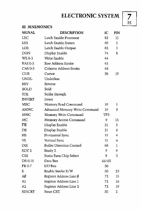
ill MNEMONICS
SIGNAL DESCRIPTION IC PIN LEC Latch Enable Processor 82 11
LES Latch Enable Screen 69 1
LOE Latch Enable Output 82 1
DON Display Enable 74 8
WE 0-3 Write Enable 44
RAS 0-3 Row Address Strobe 45
CAS 0-3 Column Address Strobe 46
CUR Cursor 30 19
UNDL Underline
REV Reverse
BOLD Bold
STK Strike through
INVERT Invert
MRC Memory Read Command 19 1
AMWC Advanced Memory Write Command 19 9
MWC Memory Write Command TP3
MC Memory Access Command 9 15
DE Display Enable 21 5
DE Display Enable 21 6
HS Horizontal Sync 11 4
VS Vertical Sync 11 6
DIR Buffer Direction Control 66 1
RDY2 Ready 2 9 9
CSS Static Ram Chip Select 9 3
DB 0-15 Data Bus 66/65
PB 0-7 I/O Bus 30
E Enable Strobe R/W 30 23
A¢ Register Address Line ¢ 72 15
Al Register Address Line 1 72 16
A2 Register Address Line 2 72 19
RESCRT Reset CRT 30 2
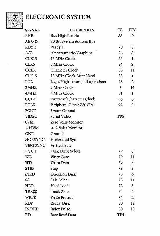
rn ELECTRONIC SYSTEM 36
SIGNAL DESCRIPTION IC PIN
BHE Bus High Enable 33 9
AB 0-19 20 Bit System Address Bus
RDYI Ready 1 20 3
A/G Alphanumeric/Graphics 26 3
CLK15 15 MHz Clock 25 1
CLK5 5 MHz Clock 84 2
CCLK Character Clock 35 11
CLK15 15 MHz Clock After Nand 25 4
PU2 Logic High - from pull up resister 25 2
2MHZ 2 MHz Clock 7 14
4MHZ 4 MHz Clock 81 1
CCLK Inverse of Character Clock 35 6
PCLK Peripheral Clock Z80 SIlO 92 2
FGND Frame Ground
VIDEO Serial Video TP5
OVM Zero Volts Monitor
+ 12VM +12 Volts Monitor
GND Ground
HORSYNC Horizontal Syn
VERTSYNC Vertical Syn
DS 0-1 Disk Drive Select 79 3
WG Write Gate 79 11
WD Write Data 79 8
STEP Step 73 3
DIRD Direction Disk 73 6
SS Side Select 73 11
HLD Head Load 73 8
TRK¢¢ Track Zero 74 4
WRPR Write Protect 74 2
RDY Ready Disk 80 12
INDEX Index Pulse 80 10
RD Raw Read Data TP4
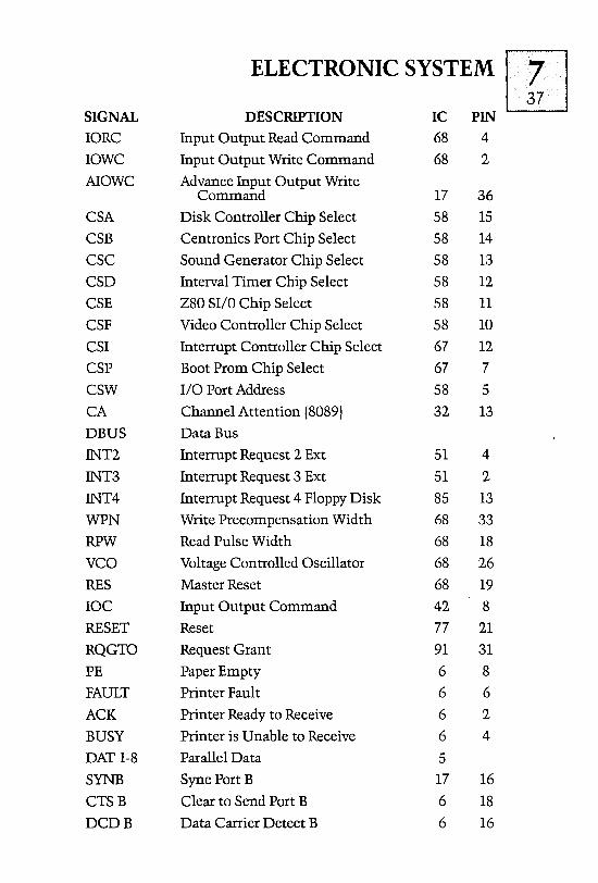
ELECTRONIC SYSTEM [IJ SIGNAL DESCRIPTION IC PIN
lORC Input Output Read Command 68 4
lOWC Input Output Write Command 68 2
AlOWC Advance Input Output Write Command 17 36
CSA Disk Controller Chip Select 58 15
CSB Centronics Port Chip Select 58 14
CSC Sound Generator Chip Select 58 13
CSD Interval Timer Chip Select 58 12
CSE Z80 SIlO Chip Select 58 11
CSF Video Controller Chip Select 58 10
CSl Interrupt Controller Chip Select 67 12
CSP Boot Prom Chip Select 67 7
CSW 110 Port Address 58 5
CA Channel Attention (8089) 32 13
DBUS Data Bus
INT2 Interrupt Request 2 Ext 51 4
INT3 Interrupt Request 3 Ext 51 2
INT4 Interrupt Request 4 Floppy Disk 85 13
WPN Write Precompensation Width 68 33
RPW Read Pulse Width 68 18
VCO Voltage Controlled Oscillator 68 26
RES Master Reset 68 19
lOC Input Output Command 42 8
RESET Reset 77 21
RQGTD Request Grant 91 31
PE Paper Empty 6 8
FAULT Printer Fault 6 6
ACK Printer Ready to Receive 6 2
BUSY Printer is Unable to Receive 6 4
DAT 1-8 Parallel Data 5
SYNB Sync Port B 17 16
CTSB Clear to Send Port B 6 18
DCDB Data Carrier Detect B 6 16
ELECTRONIC SYSTEM
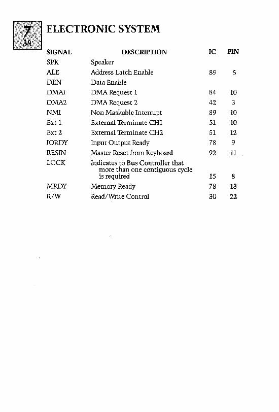
SIGNAL DESCRIPTION IC PIN
SPK Speaker
ALE Address Latch Enable 89 5 DEN Data Enable
DMAI DMA Request 1 84 10
DMA2 DMA Request 2 42 3
NMI Non Maskable Interrupt 89 10
Ext 1 External Terminate CHI 51 10
Ext 2 External Terminate CH2 51 12
IORDY Input Output Ready 78 9
RESIN Master Reset from Keyboard 92 11
LOCK Indicates to Bus Controller that more than one contiguous cycle is required 15 8
MRDY Memory Ready 78 13
R/W Read/Write Control 30 22
ELECTRONIC SYSTEM m W
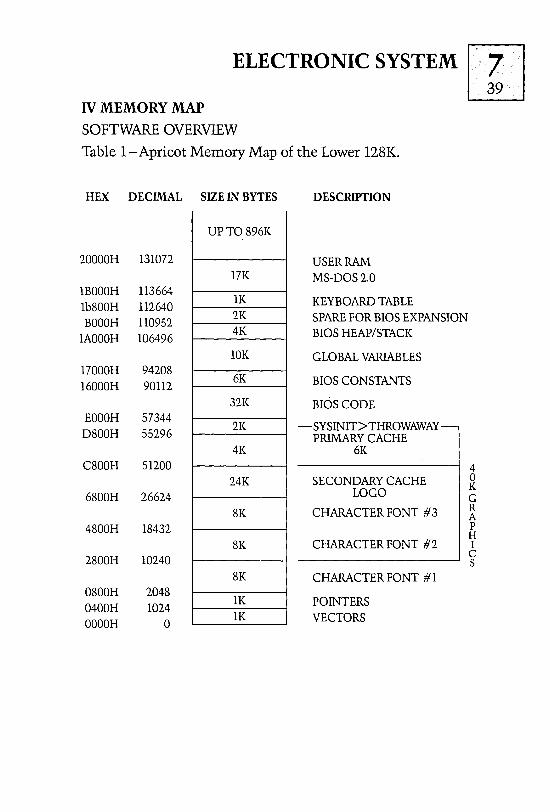
IV MEMORY MAP SOFTWARE OVERVIEW
Table 1-Apricot Memory Map of the Lower 128K.
HEX DECIMAL SIZE IN BYTES
UP TO 896K
20000H 131072 17K
1BOOOH 113664 1b800H 112640 BOOOH 110952
1AOOOH 106496
1K 2K 4K
10K 17000H 94208 16000H 90112
6K
32K EOOOH 57344 D800H 55296
2K
4K C800H 51200
24K 6800H 26624
8K 4800H 18432
8K 2800H 10240
8K 0800H 2048 0400H 1024 OOOOH 0
1K 1K
DESCRIPTION
USER RAM MS-DOS 2.0
KEYBOARD TABLE SPARE FOR BIOS EXPANSION BIOS HEAP/STACK
GLOBAL VARIABLES
BIOS CONSTANTS
BIOS CODE
-SYSINIT>THROWAWAY PRIMARY CACHE
6K
SECONDARY CACHE LOGO
CHARACTER FONT #3
CHARACTERFONT #2
4 o K G R A p H I C
----------------~ S
CHARACTER FONT #1
POINTERS VECTORS

'"'"---S_E_'f._-U_P_P_R_O_C_E_D_U_RE_S __ ---'1 [!] I Keyboard Clock Set-Up Procedure
II Floppy Disk Controller Set-Up Procedure
SET-UP PROCEDURES W I KEYBOARD CLOCK OSCILLATOR SET-UP
1. Apply power to keyboard (no data).
2. Frequency counter/scope to pin 37 of 6301.
3. Adjust variable cap (C2) to give 976.562 uS + .01 uS i.e. 976.55-976.57 uS.
t~~~~,J SET-UP PROCEDURES
n FLOPPY DISK-CONTROLLER SET-UP REVE
1. Switch on.
2. Short out pins 1 and 2.
3. Scope/frequency counter to pin 3.
4. Adjust variable capacitor (VCI) to give 2 uS period (500 KHz) + 100 nS.
5. Scope to pin 4.
6. Adjust WPW (Write Precompensation - VR2) to give 125 nS + 10 nS.
7. Scope to pin 5.
8. Adjust RPW (Read Pulse - VR1) to give 250 nS + 10 nS.
FLOPPY DISK - CONTROLLER SET-UP REV G
1. Switch on.
2. Short out pins 1 and 2.
3. Scope/frequency counter to pin 4.
4. Adjust variable capacitor (VCI) to give 2 uS period (500 KHz) + 100 nS.
5. Scope to pin 5.
6. Adjust WPW (Write Precompensation-VR2) to give 125 nS + 10 nS.
7. Scope to pin 3.
8. Adjust RPW (Read Pulse-VR1) to give 250 nS + 10 nS.
SET-UP PROCEDURES
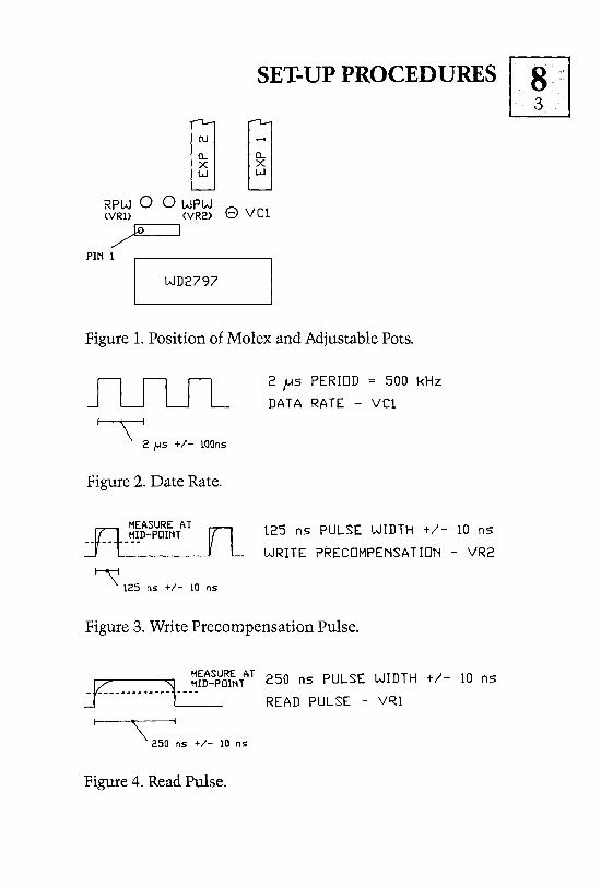
RPW 0 0 WPW (VRl) (VR2) e vel
/' lli I
PIN t
WD2797
Figure 1. Position of Molex and Adjustable Pots.
\. 2,..s +1- lOOns
Figure 2. Date Rate.
n MEASURE AT n MID-POINT -- -- ----
~ 125 ns +/- 10 ns
2 ~s PERIOD = 500 kHz
DATA RATE - VCl
125 ns PULSE WIDTH +/- 10 ns
WRITE PRECOMPENSATION - VR2
Figure 3. Write Precompensation Pulse.
MEASURE AT 250 ns PULSE WIDTH +/- 10 ns f ____ u ____ 1 __ .::ID-POlNT READ PULSE - VRl
1--_\------11 250 ns -+/- 10 ns
Figure 4. Read Pulse.

~D_~ __ G_N_O_ST_I_C __________ ~I~ I Diagnostic Boot Prom Documentation and
Error Codes
II Diagnostic Programs
DIAGNOSTIC
I DIAGNOSTIC BOOT PROM DOCUMENTATION AND ERROR CODES
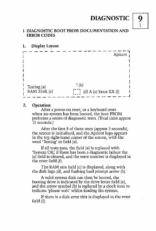
1. Display Layout 1- - - - - - - --------------,
Apricot I I I I I I I I 1
I
I I I I I
Testing (aJ i (b) I RAM 256K (c) r- -j (d) A (e) Error XX (fJ 1
L _ _ -I
-------------------~ 2. Operation
After a power-on reset, or a keyboard reset when no system has been booted, the boot PROM performs a series of diagnostic tests. (Total time approx 11 seconds.)
After the first 8 of these tests (approx 5 seconds), the screen is initialised, and the Apricot logo appears in the top right-hand comer of the screen, with the word 'Testing' in field (aJ.
If all tests pass, the field (a) is replaced with 'System OK; if there has been a diagnostic failure the (aJ field is cleared, and the error number is displayed in the error field (f).
The RAM size field (c) is displayed, along with the disk logo (d), and flashing load prompt arrow (b).
A valid system disk can then be booted, the booting drive is indicated by the drive letter field (eJ, and the arrow symbol (b) is replaced by a clock icon to indicate 'please wait' whilst loading the system.
If there is a disk error this is displayed in the error field (f).
I?il DIAGNOSTIC
If calc mode is entered before boot then fields (b) - (f) are cleared, -fields (b) - (e) are restored on leaving calc mode.
On a reset after a system boot, none of the diagnostic tests are executed, and the program jumps straight to the 'load disk' prompt-field (a) is not used.
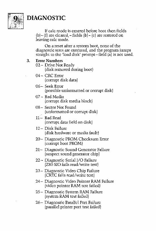
3. Error Numbers 02- Drive Not Ready
(disk removed during boot)
04 - CRC Error (corrupt disk data)
06 - Seek Error (possible unformatted or corrupt disk)
07 - Bad Media (corrupt disk media block)
08- Sector Not Found (unformatted or corrupt disk)
11- Bad Read (corrupt data field on disk)
12 - Disk Failure (disk hardware or media fault)
20 - Diagnostic PROM Checksum Error (corrupt boot PROM)
21- Diagnostic Sound Generator Failure (suspect sound generator chip)
22 - Diagnostic Serial I/O Failure (Z80 SIO fails read/write test)
23 - Diagnostic Video Chip Failure (CRTC fails read/write test)
24 - Diagnostic Video Pointer RAM Failure (video pointer RAM test failed)
25 - Diagnostic System RAM Failure (system RAM test failed)
26 - Diagnostic Parallel Port Failure (parallel printer port test failed)

DIAGNOSTIC
27 - Diagnostic Interrupt Controller Failure (8259A PIC failed read/write test)
28 - Diagnostic Floppy Disk Controller Failure (FDC failed read/write/seek test)
29 - Diagnostic Counter Timer Failure (CTC failed read/write test)
30 - Diagnostic Serial Channel Failure (channel A of Z80 SIO failed test)
31- Diagnostic Keyboard Failure (keyboard initialisation test failed)
32 - Diagnostic Timer Accuracy Failure (CTC accuracy check against timing loop failed)
33- Diagnostic Timer/PIC Interaction Failure (CTC/PIC timing interaction test failed)
34 - Diagnostic 10 Processor Failure (8089 lOP failed init/memory move test)
99 - Non-System Disk (disk is not a valid system disk)
Note: Tests 21, 26, 30 and 33 are not fully implemented and should never fail at present.

EXPANSION BOARDS I ~
1. General Installation Instructions
2. Expansion Board Power Requirements
3. 256K RAM
4. 128K/512K RAM
5. Modem
6. Lan Board
Expansion Board 1

1 . General Recommendations
2. Apricot PC - Apricot Xi
3.ApricotF1-ApricotF1e
4. Apricot Portable
1. General Recommendations 1 . It is recommended that installation of any expansion board
be carried out by an authorised dealer.
Warning - Remove Power Cable Before Attempting To Gain Access To The Expansion Slots.
2. Unless specifically noted, assembly is the reverse of disassembly.
3. Do not mix screws (length, diameter).
4. A number in parenthesis, thus (4) indicates the number of screws to be slackened or removed to remove that particular part.
5. The expansion slot is polarised to prevent incorrect insertion.
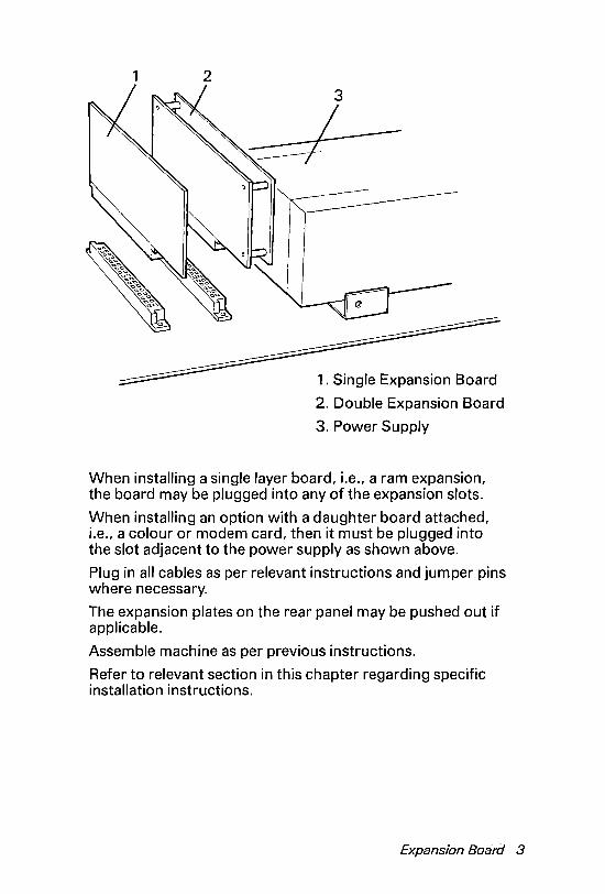
6. A single or double board may be installed into any Apricot.
7. Check all expansion board pins are straight before fitting into expansion slot.
8. Plug in all cables as per relevant instructions and jumper pins where necessary.
2. Apricot PC - Apricot Xi Removal of top cover.
1. Remove M4 x 12mm screws (3) on rear panel.
2. Allow rear panel to tilt backwards and remove top cover by lifting at rear slightly and disengaging lip from front bezel.
3. Expansion slots are adjacent to power supply.
2 Expansion Board
1 2
1 . Single Expansion Board
2. Double Expansion Board
3. Power Supply
When installing a single layer board, i.e., a ram expansion, the board may be plugged into any of the expansion slots.
When installing an option with a daughter board attached, i.e., a colour or modem card, then it must be plugged into the slot adjacent to the power supply as shown above.
Plug in all cables as per relevant instructions and jumper pins where necessary.
The expansion plates on the rear panel may be pushed out if applicable.
Assemble machine as per previous instructions.
Refer to relevant section in this chapter regarding specific installation instructions.
Expansion Board 3
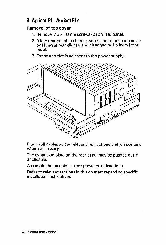
3. Apricot F1 - Apricot F1 e Removal of top cover
1. Remove M3 x 1 Omm screws (2) on rear panel.
2. Allow rear panel to tilt backwards and remove top cover by lifting at rear slightly and disengaging lip from front bezel.
3. Expansion slot is adjacent to the power supply.
Plug in all cables as per relevant instructions and jumper pins where necessary.
The expansion plate on the rear panel may be pushed out if applicable.
Assemble the machine as per previous instructions.
Refer to relevant sections in this chapter regarding specific installation instructions.
4 Expansion Board
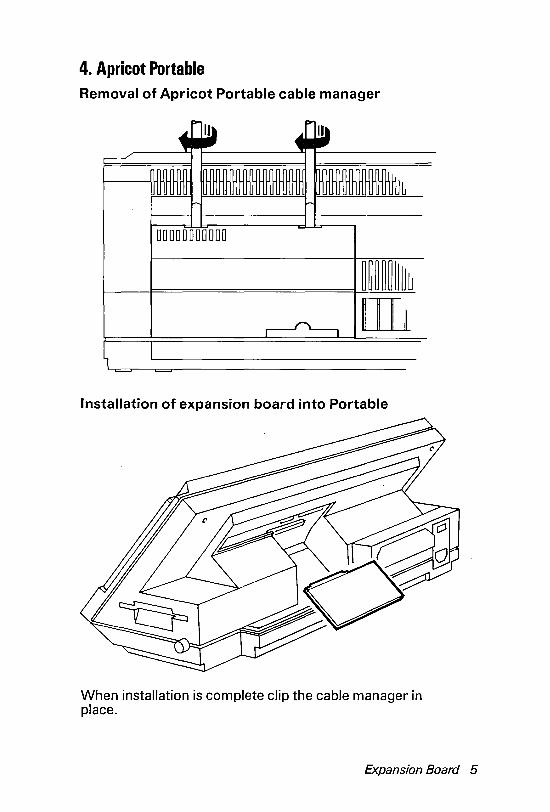
4. Apricot Portable Removal of Apricot Portable cable manager
00000000000
Installation of expansion board into Portable
When installation is complete clip the cable manager in place.
Expansion Board 5
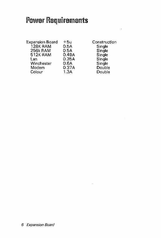
Expansion Board 128K RAM 256k RAM 512K RAM Lan Winchester Modem Colour
6 Expansion Board
+5u O.5A O.5A O.49A O.35A O.6A O.37A 1.3A
Construction Single Single Single Single Single Double Double
1. Installation
2. Theory of operation.
3. Integrated circiut catalogue.
4. Mnemonics
5. Parts list.
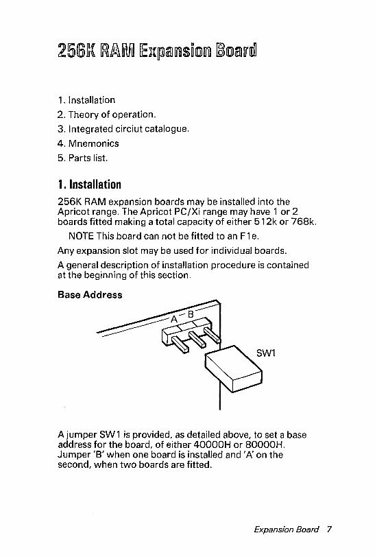
1. Installation 256K RAM expansion boards may be installed into the Apricot range. The Apricot PC/Xi range may have 1 or 2 boards fitted making a total capacity of either 512k or 768k.
NOTE This board can not be fitted to an F 1 e.
Any expansion slot may be used for individual boards.
A general description of installation procedure is contained at the beginning of this section.
Base Address
A jumper SW 1 is provided, as detailed above, to set a base address for the board, of either 40000H or 80000H. Jumper '8' when one board is installed and 'A' on the second, when two boards are fitted.
Expansion Board 7
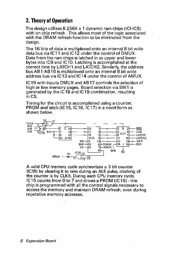
2. Theory of Operation The design utilizes 8 256K x 1 dynamic ram chips (ICI-IC8) with on chip refresh. This allows most of the logic associated with the DRAM refresh function to be eliminated from the design.
The 16 bits of data is multiplexed onto an internal 8 bit wide data bus via Ie 11 and IC 12 under the control of DMUX. Data from the ram chips is latched in as upper and lower bytes into IC9 and IC 10. latching is accomplished at the correct time by lATCH 1 and lATCH2. Similarly, the address bus AB 1-AB 16 is multiplexed onto an internal 8 bit wide address bus via IC 13 and IC 14 under the control of AMUX.
IC 19 with inputs DMUX and AB 17 controls the selection of high or low memory pages. Board selection via SW 1 is generated by the IC 18 and IC 19 combination, resulting in CS.
Timing for the circuit is accomplished using a counter, PROM and latch (lC 15, IC 16, IC 17) in a novel form as shown below.
CLK5-......-, ALE A18 A19
D1
1----t>--l10 1----c>-j11 t-------I>--i 12
IC16 WE 5
SHE 14 OV 15
MRDY -'--:-:-<11
A valid CPU memory cycle synchronizes a 3 bit counter
RAS CAS LATCH1 LATCH 2 AS0 SHE
(lC15) by clearing it to zero during an ALE pulse, clocking of the counter is by ClK5. During each CPU memory cycle, IC 15 counts from 0 to 7 and drives a PROM (Ie 16) - this chip is programmed with all the control signals necessary to access the memory and maintain DRAM refresh, even during repetative memory accesses.
8 Expansion Board
3. Integrated Circuit Catalogue
I IC I 1,2,3,4,5,6,7,8.
HM50256-20 256K x 1 Dynamic Random Access Memory.
Forms 256K x 8 memory
I IC I 9,10
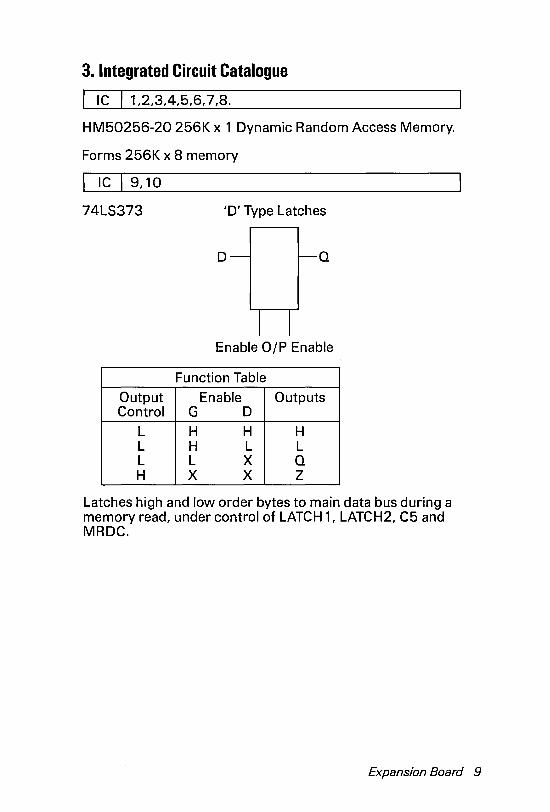
74LS373 'D' Type Latches
D Q
Enable DIP Enable
Function Table
Output Enable Outputs Control G D
L H H H L H L L L L X Q H X X Z
Latches high and low order bytes to main data bus during a memory read, under control of LATCH 1 , LATCH2, C5 and MRDC.
Expansion Board 9
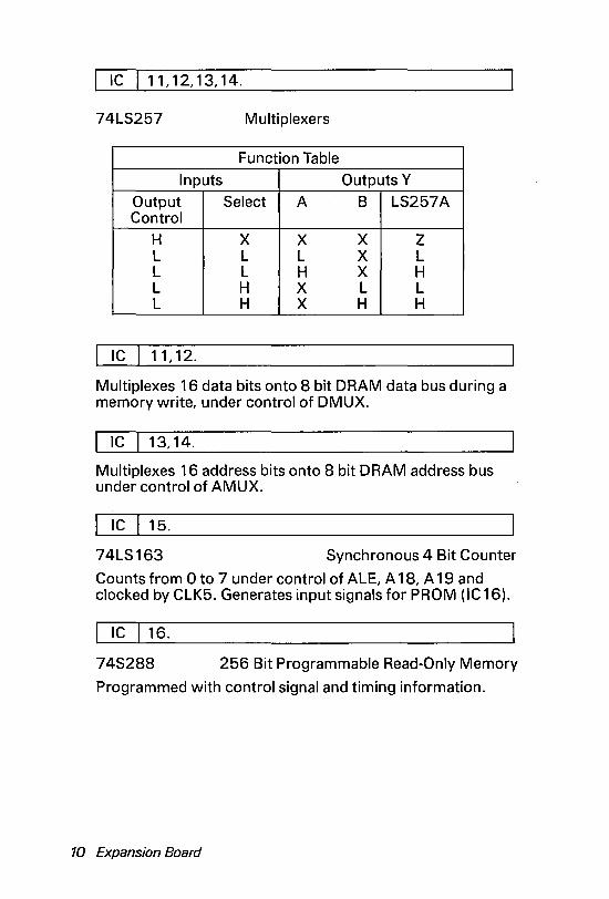
IC 11,12,13,14.
74LS257 Multiplexers
Function Table
Inputs Outputs Y
Output Select A B LS257A Control
H X X X Z L L L X L L L H X H L H X L L L H X H H
IC 11,12.
Multiplexes 16 data bits onto 8 bit DRAM data bus during a memory write, under control of DMUX.
I IC I 13,14.
Multiplexes 16 address bits onto 8 bit DRAM address bus under control of AMUX.
1 IC 115. 74LS 163 Synchronous 4 Bit Counter
Counts from 0 to 7 under control of ALE, A 18, A 19 and clocked by CLK5. Generates input signals for PROM (IC 16).
1 IC 116. 74S288 256 Bit Programmable Read-Only Memory
Programmed with control signal and timing information.
10 Expansion Board
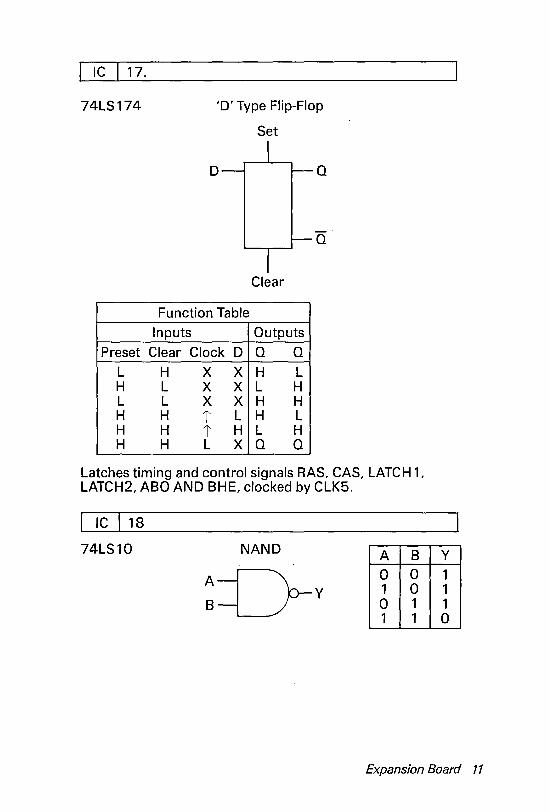
IC 117.
74LS174 '0' Type Flip-Flop
Set
o Q
Clear
Function Table
Inputs Outputs
Preset Clear Clock 0 Q Q
L H X X H L H L X X L H L L X X H H H H l' L H L H H l' H L H H H L X Q Q
Latches timing and control signals RAS, CAS, LATCH 1, LATCH2, ABO AND BHE, clocked by CLK5.
1 IC 118 74LS10 NAND A B
:=D-v 0 0 1 0 0 1 1 1
Y 1 1 1 0
Expansion Board 11
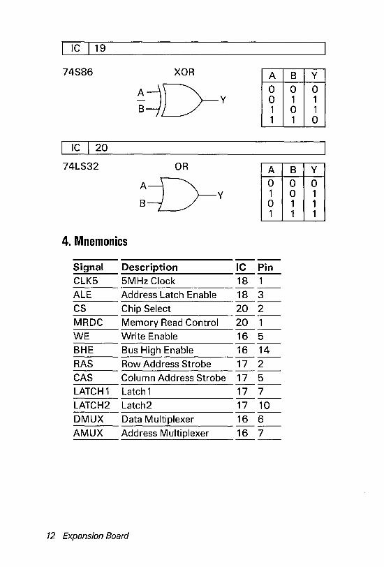
IC I 19
74S86 XOR A B Y 0 0 0 0 1 1 1 0 1 1 1 0
IC 20
74LS32 OR A B y
:=[)-v 0 0 0 1 0 1 0 1 1 1 1 1
4. Mnemonics
---Signal Description Ie Pin ---CLK5 5MHz Clock 18 1
---ALE Address Latch Enable 18 3 ---CS Chip Select 20 2
---MRDC Memory Read Control 20 1 ---WE Write Enable 16 5 ---BHE Bus High Enable 16 14 ---RAS Row Address Strobe 17 2 ---CAS Column Address Strobe 17 5 ---LATCH1 Latch 1 17 7 ---LATCH2 Latch2 17 10 ---DMUX Data Multiplexer 16 6
---AMUX Address Multiplexer 16 7 ---
12 Expansion Board
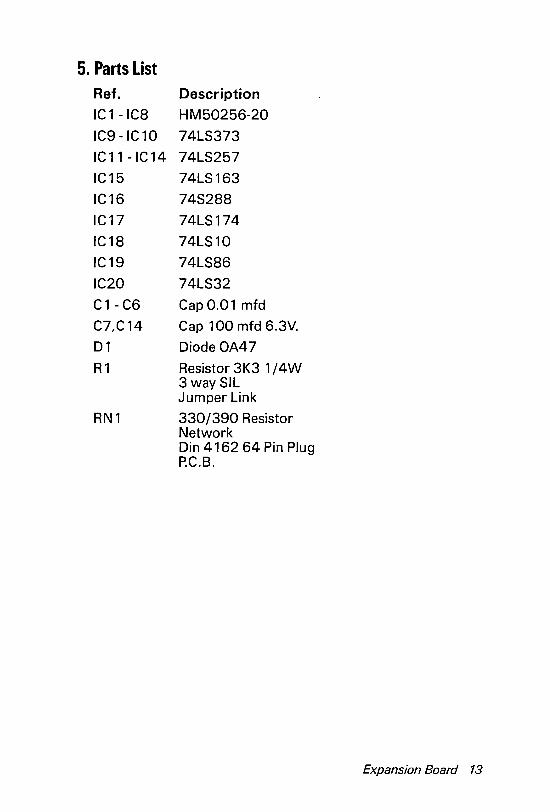
5. Parts List Ref. Description
IC 1 -IC8 HM50256-20
IC9-IC10 74LS373
IC11 -IC14 74LS257
IC15 74LS163
IC16 74S288
IC17 74LS174
IC18 74LS10
IC19 74LS86
IC20 74LS32
C1-C6 Cap 0.01 mfd
C7,C14 Cap 100 mfd 6.3V.
01 Diode OA47
R1 Resistor 3K3 1/4W 3 way SIL Jumper Link
RN1 330/390 Resistor Network Din 4162 64 Pin Plug P.C.B.
Expansion Board 13
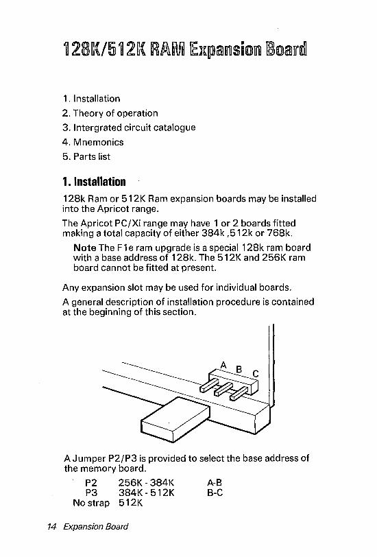
1. Installation
2. Theory of operation
3. Intergrated circuit catalogue
4. Mnemonics
5. Parts list
1. Installation 128k Ram or 512K Ram expansion boards may be installed into the Apricot range.
The Apricot PC/Xi range may have 1 or 2 boards fitted making a total capacity of either 384k ,512k or 768k.
Note The F 1 e ram upgrade is a special 128k ram board with a base address of 128k. The 512K and 256K ram board cannot be fitted at present.
Any expansion slot may be used for individual boards.
A general description of installation procedure is contained at the beginning of this section.
A Jumper P2/P3 is provided to select the base address of the memory board.
P2 256K-384K ~8 P3 384K - 512K 8-C
No strap 512K
14 Expansion Board
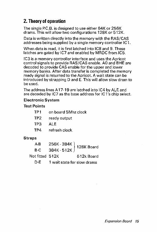
2. Theory of operation The single P.C.B. is designed to use either 64K or 256K drams. This will allow two configurations 128K or 512K.
Data is written directly into the memory with the RASjCAS addresses being supplied by a single memory controller IC 1.
When data is read, it is first latched into IC8 and 9. These latches are gated by IC7 and enabled by MRDC from IC5.
IC3 is a memory controller interface and uses the Apricot control signals to provide RASjCAS enable. AD and BHE are decoded to provide CAS enable for the upper and lower memory banks. After data transfer is completed the memory ready signal is returned to the Apricot. A wait state can be introduced by strapping D and E. This will allow slow dram to be used.
The address lines A 17-19 are latched into IC4 by ALE and are decoded by IC7 as the base address for IC 1's chip select.
Electronic System
Test Points
TP 1 on board 5Mhz clock
TP2 ready output
TP3 ALE
TP4 refresh clock.
Straps
A-B 256K - 384K} 128K Board B-C 384K-512K
Not fitted 512K 512k Board
D-E 1 wait state for slow drams
Expansion Board 15
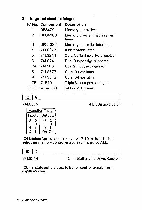
3. Intergrated circuit catalogue IC No. Component Description
1 DP8409 Memory controller
2 DP84300 Memory programmable refresh timer
3 DP84332 Memory controller interface
4 74LS375 4-bit bistable latch
5 74LS244 Octal buffer line driver/receiver
6 74LS74 Dual D-type edge triggered
7A 74LS86 Qual 2-input exclusive -or
8 74LS373 Octal D-type latch
9 74LS373 Octal D-type latch
7B 74S10 Triple 3 input pos nand gate
11-26 4164-20 64K/256K drams.
IC 14
74LS375 4 Bit Bistable Latch
Function Table Inputs Outputs D G Q Q L H L H H H H L X L 00 00
IC4 latches Apricot address lines A 17-19 to decode chip select for memory controller address latched by ALE.
1 IC 1 5
74LS244 Octal Buffer Line Drive/Receiver
IC5. Tri state buffers used to buffer control signals from expansion bus.
16 Expansion Board
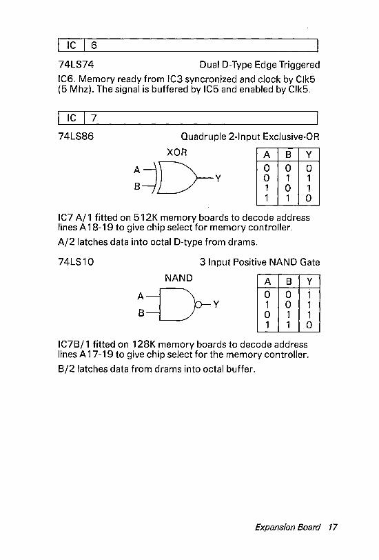
IC 6
74LS74 Dual D-Type Edge Triggered
IC6. Memory ready from IC3 syncronized and clock by Clk5 (5 Mhz). The signal is buffered by IC5 and enabled by Clk5.
I IC 17 74LS86 Quadruple 2-lnput Exclusive-OR
XOR A B y
0 0 0 0 1 1 1 0 1 1 1 0
IC7 AI 1 fitted on 512K memory boards to decode address lines A 18-19 to give chip select for memory controller.
A/2 latches data into octal D-type from drams.
74LS10 3 Input Positive NAND Gate
NAND A B y
~D-Y 0 0 1 1 0 1 0 1 1 1 1 0
IC7B/1 fitted on 128K memory boards to decode address lines A 17-19 to give chip select for the memory controller.
B/2 latches data from drams into octal buffer.
Expansion Board 17
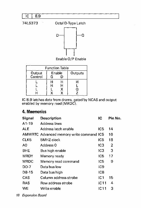
IC 8,9
74LS373 Octal D-Type Latch
o Q
Enable O/P Enable
Function Table
Output Enable Outputs Control G 0
L H H H L H H L L L X Q H X X Z
IC 8,9 latches data from drams, gated by NCAS and output enabled by memory read (MRDC)'
4. Mnemonics Signal Description Ie Pin No.
A 1-19 Address lines
ALE Address latch enable IC5 14
AMWRTC Advanced memory write command IC5 16
CLK5 5MHZ clock IC5 18
AD Address D IC3 2 BHE Bus high enable IC3 3
MRDY Memory ready IC5 17
MRDC Memory read command IC5 9
00-7 Data bus low IC9
08-15 Data bus high Ica CAS Column address strobe IC1 15
RAS Row address strobe IC 11 4
WE Write enable IC 11 3
18 Expansion Board
Signal Description Ie PinNo.
OE Output enable ICg
G Gate enable ICg 11
RO-8 Row address byte IC1
CO-8 Column address byte IC1
CS Chip select IC1 47
WIN Write enable input IC1 45
RGCK RAS generator clock IC1 2 RFCK Refresh clock IC1
RFSH Refresh IC1 5
MO Mode control IC1 3
RASIN Row address strobe in IC1 48
MAO-8 Memory address IC1
RFRQ Refresh request IC3 8
CASL Column address strobe lower IC3 13
CASU Column address strobe upper IC3 14
RDY Ready IC3 15
WAIT Wait state IC3 7
Expansion Board 19
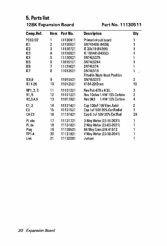
5. Parts list 128K Expansion Board Part No. 11130511
Comp.Ref. Item Part No. Description Dty
PC02/02 1 11130411 Printed circuit board ICl 2 11130621 SN74S409184091 IC2 3 11130721 IC 20xl 01843001 IC3 4 11130821 IC 16RA81843321 IC4 5 11130921 SN74lS375 IC5 6 11015121 SN74lS244 IC6 7 11131021 SN74lS74 IC7 8 11 013521 SN74lS10
Fitted in Right Hand Position IC8,9 9 11015521 SN74lS373 2 IC11-26 10 11012521 4164-20 Dram 16
RP1,2,3 11 11131221 Res Pak 47R x 4 Sil 3 Rl,5 12 11131321 Res 1 Oohm 1/4W 10% Carbon 2 R2,3,4,6 13 11017021 Res 3K3 1/4W 10% Carbon 4
Cl,2 14 11131421 Cap 1 OOuF 1 OV Elec.Axial 2 C3 15 11131521 Cap 1 uF 50V 20% Cer.Radial 1 C4-23 16 11131621 Cap 0.1 uF 50V 20% Cer.Rad 20
Plabc 17 11131721 3 Way Wafer 122-10-20311 Plde 18 11131821 2 Way Wafer 122-03-20211 Plug 19 11126521 64 Way Conn.DlN 41612 TPl-4 20 11131921 4 Way Wafer 122-10-20411 link 21 11132081 Jumper
20 Expansion Board

1. Installation
2. Technical Details
1. Installation Modem boards may be installed into the Apricot range. If the board is fitted into an Apricot PC or Xi, slot 2 ( that nearest to the power supply) must be used.
A general description of installation procedure is contained at the beginning of this section. Warning - Do Not
Connect the Telephone Cord To British Telecom Socket Until The Modem Has Been Correctly Installed In The Apricot Computer
Warning - Thi~ Modem Is Not Suitable For Use With Some Call Connect Systems With Digital Setup And Cleardown Commands.
If the Modem is fitted into the Apricot PC, Xi, F 1 or F 1 e the expansion plate on the rear panel must be removed and the modems telephone cord fed through the resultant hole. The expansion plate must then be replaced by a plate as shown in the diagram below - with a hole to allow the telephone cord to pass through it.
Expansion Plate
Expansion Board 21

If the Modem is fitted into the Apricot Portable the telephone cord may be fed through the cable manager.
When the Modem has been correctly inserted into the machine the approval sticker must be fixed onto the rear panel.
Finally the telephone and Modem must be connected into the telephone socket.
Installation is now complete.
2. Technical Details Electrical Details:
1. Modulation: Frequency Shifted Keyed (FSK) with the following frequency parameters:
Mode Baud Transmit Frequency* Receive Frequency* Answer Rate Space Mark Space Mark Tone*
CCITTV21 Originate 300 1180 980 1850 1650 Answer 300 1850 1650 1180 980 2225
CCITTV23 Originate 7511200 450 390 2100 1300 Answer 1200175 2100 1300 450 390 2100
CCITTV23 1200 2100 1300 2100 1300 2100 Half duplex
*Hz.
2. Data Format: Serial Asynchronous.
3. Minimm Recieve level: ·43dBm.
4. Maximum Transit level: ·13dBm.
Mechanical Details:
1. The Apricot Modem consists of two printed circuit boards linked together.
2. The physical dimensions of the Modem are as follows:
Length; 5.9 inches (147 mm.) Max. Height; 3.0 inches (78 mm.)
Width; 1.1 inches (27 mm.) Weight; 7 ounces. (200 grams)
22 Expansion Board
Connect Details
Series 600 plug for connecting the Modem to the telehone network.
Modem Module
The modem is a communications facility to allow an Apricot computer to transmit and recieve data via the Public Switched Telephone Network (PSTN).
Inspect the modem module to make sure no damage has occured in transit. If damage has occured, return the complete package.
B.A.B.T. Approval No. S/ 1397 /3/E/500039 Model No. ADM/4.
B.T. Circuit
The modem is only to be used with 2 wire PSTN circuits. The modem generates CCITT V25 answer sequences when set in auto answer mode and may be used on lines listed in British Telecom telephone directories. It must not be used with payphones, partylines or certain types of call connect systems that do not use two wire signalling systems.
Bell Tinkle
When the modem is used with telephones that use a mechanical bell 'bell tinkle' will be caused when dialling.
Ringer Equivalence
Equipment for attachment to the public telephone network is assesed to determin its 'ringer equivalence' number (REN). The REN indicates, in effect, the load that the telephone exchange sees when ringing the equipment. It is not permitted to put more than a total of 4 REN onto the exchange line. The modem has a REN of 3 and care must be taken not to use it with other telephone equipment that would result in the maximum figure of 4 REN being exceeded.
Expansion Board 23
Important
The approval of this modem for connection to the British Telecom public switched telephone network is INVALIDATED if the apparatus is subject to any modifications in any way not authorised by BABT or it is used with or connected to:-1. Internal software that has not been formally accepted by
BABT. 2. External control software or external control apparatus
which causes the operation of the modem or associated call set-up equipment to contravene the requirements of the standard set out in BABT /SITS/82/005s/B
24 Expansion Board

1 . Installation
2. Theory of Operation
3. Connector Pinouts
4. Integrated Circuit Catalogue
5. Mnemonics
6. Parts List
7. Network Diagram.
1. Installation One local area network board (Lan) can be installed into the Apricot to create a structure so that files/programs can be shared with other people in a local area network.
Any expansion slot may be used for individual boards.
After checking the network device address follow the general installation instructions at the beginning of this section.
When the board has been correctly installed;
1. Connect the Ian tap cable to the rear of the Ian board.
2. Insert the tap cable into the Ian tap box.
Network Device Addresses
The device address is set on a dip switch (SW1) shown as address 63.
Expansion Board 25
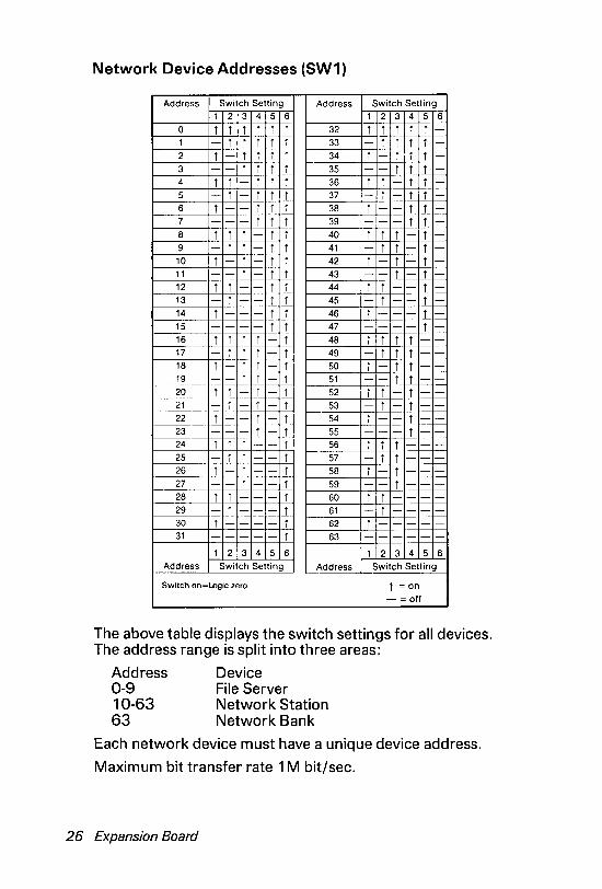
Network Device Addresses (SW1)
Address Switch Setting Address Switch Setting 1 2 3 4 5 6 1 2 3 4 5 6
0 f f f f f f 32 f f f f f -1 - i f f f f 33 - i i f f -2 f - f f i i 34 i - f f f -
3 -- f f f f 35 -- f f i -4 i f - i f f 36 f i - f f -5 - f - f i i 37 - i - i i -6 i --i i f 38 i -- f i -7 -- - f f i 39 -- - i f -8 f f f - f f 40 f f f - f -9 - f f - f f 41 - f f - f -10 f - f - f f 42 f - f - f -11 -- i - f f 43 -- f - i -12 f f -- f f 44 f f -- f -
13 - f -- f f 45 - f -- f -14 f -- - f f 46 f -- - f -15 -- -- f i 47 -- -- i -16 f f f f - f 48 f f f f --17 - i i f - f 49 - f f f --18 f - f i - i 50 f - f f --19 -- f i - i 51 -- f f --20 f f - i - f 52 f f - i --21 - f - i - i 53 - f - f --22 f -- f - f 54 f -- f --23 -- - f - f 55 -- - f --24 i i f -- i 56 i i f -- -25 - f f -- i 57 - f i -- -26 f - f -- f 58 i - f -- -27 -- i -- f 59 -- i -- -28 f i -- - f 60 i i -- --29 - i -- - i 61 - i -- --30 i -- -- i 62 i -- -- -31 -- -- - i 63 -- -- --
1 2 3 4 5 6 1 2 3 4 5 6 Address Switch Setting Address Switch Setting
Switch on=l.ogic zero i = on -=off
The above table displays the switch settings for all devices. The address range is split into three areas:
Address Device 0-9 File Server 10-63 Network Station 63 Network Bank
Each network device must have a unique device address.
Maximum bit transfer rate 1 M bit/sec.
26 Expansion Board
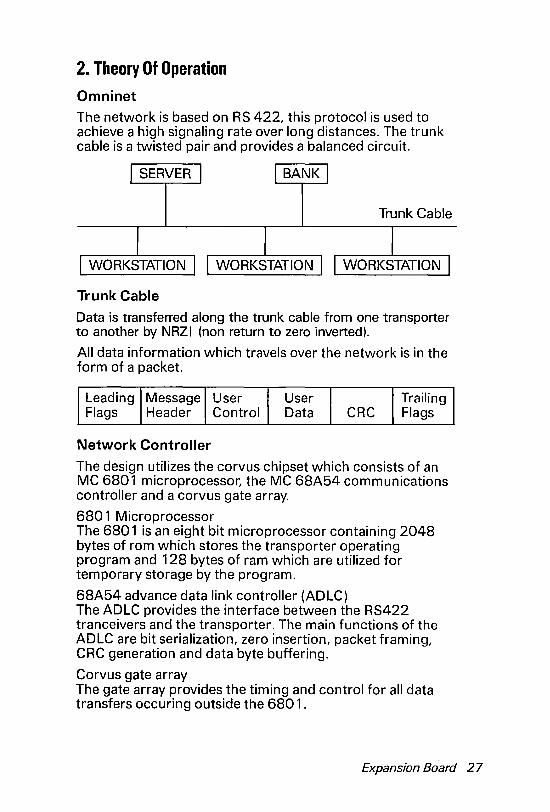
2. Theory Of Operation Omninet
The network is based on RS 422, this protocol is used to achieve a high signaling rate over long distances. The trunk cable is a twisted pair and provides a balanced circuit.
Trunk Cable
Trunk Cable
Data is transferred along the trunk cable from one transporter to another by NRZI (non return to zero inverted).
All data information which travels over the network is in the form of a packet.
Network Controller
The design utilizes the corvus chipset which consists of an MC 6801 microprocessor, the MC 68A54 communications controller and a corvus gate array.
6801 Microprocessor The 6801 is an eight bit microprocessor containing 2048 bytes of rom which stores the transporter operating program and 128 bytes of ram which are utilized for temporary storage by the program.
68A54 advance data link controller (ADLC) The ADLC provides the interface between the RS422 tranceivers and the transporter. The main functions of the ADLC are bit serialization, zero insertion, packet framing, CRC generation and data byte buffering.
Corvus gate array The gate array provides the timing and control for all data transfers occuring outside the 6801.
Expansion Board 27
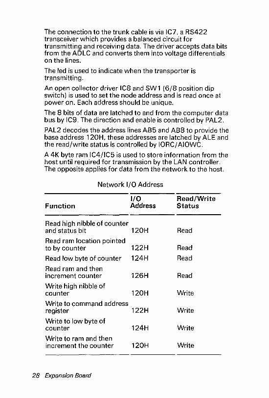
The connection to the trunk cable is via IC7, a RS422 transceiver which provides a balanced circuit for transmitting and receiving data. The driver accepts data bits from the ADLC and converts them into voltage differentials on the lines.
The led is used to indicate when the transporter is transmitting.
An open collector driver IC8 and SW1 (6/8 position dip switch) is used to set the node address and is read once at power on. Each address should be unique.
The 8 bits of data are latched to and from the computer data bus by ICg. The direction and enable is controlled by PAL2.
PAL2 decodes the address lines AB5 and AB8 to provide the base address 120H, these addresses are latched by ALE and the read/write status is controlled by 10RC/ AIOWC.
A 4K byte ram IC4/IC5 is used to store information from the host until required for transmission by the LAN controller. The opposite applies for data from the network to the host.
Network I/O Address
Function
Read high nibble of counter and status bit
Read ram location pointed to by counter
Read low byte of counter
Read ram and then increment counter
Write high nibble of counter
Write to command address register
Write to low byte of counter
Write to ram and then increment the counter
28 Expansion Board
I/O Address
120H
122H
124H
126H
120H
122H
124H
120H
Read/Write Status
Read
Read
Read
Read
Write
Write
Write
Write
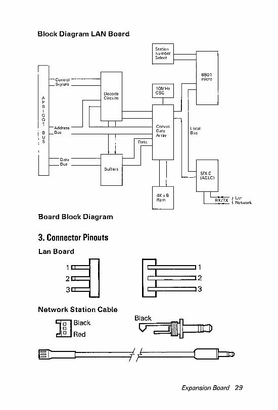
Block Diagram LAN Board
Station Number Select
6801 Control micro Signals -
lOMHz .----Decode OSC
- Circuits I
A p R -I -C 0 -
- Corvus Local Gate Bus Array
;---
Data
T Address
B Bus U S
-
Data -Bus -
Buffers
Board Block Diagram
3. Connector Pinouts
Lan Board
Network Station Cable
'lfl Black
d§JRed
- SDLC - (ADLC)
4Kx8
I Ram RX/TX I Lan \ Network
C::::====::::::J 1 ,...-11....-----,2
,...-11....----...., 3
BlaCk~ V ~~.&...IofoIlC...,]l
~1~~I--~----~II~------[~~IPo
Expansion Board 29
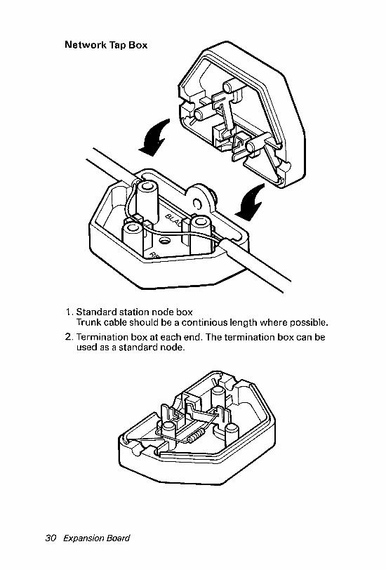
Network Tap Box
1. Standard station node box Trunk cable should be a continious length where possible.
2. Termination box at each end. The termination box can be used as a standard node.
30 Expansion Board
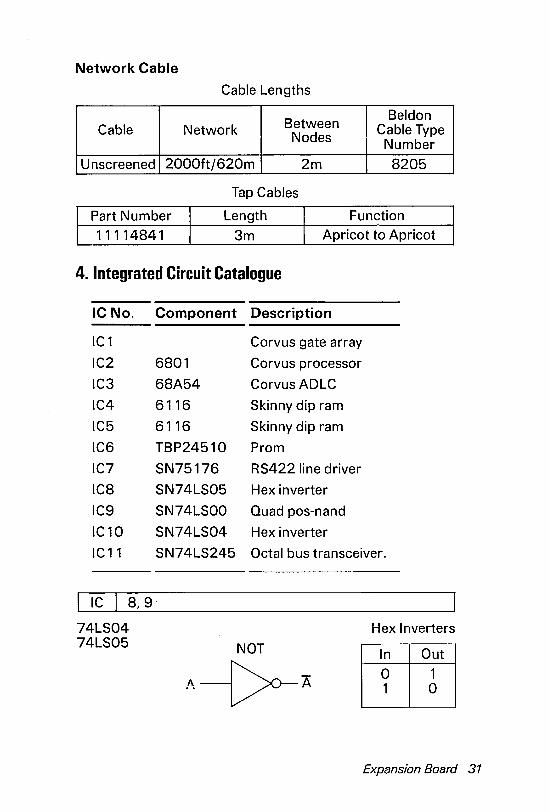
Network Cable
Cable Lengths
Between Beldon
Cable Network Cable Type Nodes Number
Unscreened 2000ft/620m 2m 8205
Tap Cables
Part Number Length I Function 11114841 3m I Apricot to Apricot
4. Integrated Circuit Catalogue
ICNo. Component Description
IC1 Corvus gate array
IC2 6801 Corvus processor
IC3 68A54 Corvus ADLC
IC4 6116 Skinny dip ram
IC5 6116 Skinny dip ram
IC6 TBP24510 Prom
IC7 SN75176 RS422 line driver
IC8 SN74LS05 Hex inverter
IC9 SN74LSOO Quad pos-nand
IC10 SN74LS04 Hex inverter
IC 11 SN74LS245 Octal bus transceiver.
IC I 8,9
74LS04 74LS05 NOT
i\-V-A
Hex Inverters
In Out
0 1 1 0
Expansion Board 31
IC 10
74LSOO Quad Positive NAND
NAND A B Y
:=[)-v 0 0 1 1 0 1 0 1 1 1 1 0
IC 11
Octal Bus Transceiver
A1 B1
Function Table
Enable Direction Operation G Control
DIR
L L B Data to A Bus L H A Data to B Bus H X Isolation
IC 11 bi-directional data bus from Apricot expansion bus to corvus gate array.
I IC 17 SN75176 RS422 Balanced Line Driver
IC7 connects the twin twisted pair LAN network to the LAN board balanced non polorized signal.
I IC 14,5
6116 Skinny Dip Ram
32 Expansion Board
5. Nmemonics
---------------------Signal Description Ie Pin ---------------------ABO-8 Address bus 0-8 IC6 AIOWC Advanced I/O write command IC6 9 10RC I/O read command IC6 8 DBO-7 Data bus 0-7 IC9 INT3 Interupt 3 IC6 20 RESET Reset IC2 6 WE Write enable IC 1 2 CS Chip select IC 11 20 BRD Buffer Read IC6 14 ALE Address latch enable IC6 7 RAO-1 Ram Address IC 1 RDO-7 Ram Address IC 1 OE Output enable IC 1 3 WR Write req uest I C 1 4 HDO-7 Host Data IC 1 TXENA Transmit enable IC 1 61 RXD Receive data IC 1 62 BITCK 1 MHz clock output IC 1 63 DSR Data service request IC 1 55 RTS Request to send IC 1 59 IN/OUT Transfer IN or OUT of memory IC 1 64 EOUT 1.25 MHz clock output IC 1 57 IRQ Interrupt request IC 1 60 XTAL2 5 MHz clock IC 1 58 EIN 1.25 MHz clock IN IC 1 56 R/W Read/Write IC 1 50 AUTO Decodes which DMA mode is to begin IC 1 65 READY Ready IC2 17 A8-15 Address lines IC2 HDINT Interrupt signal to host IC2 18 XTAL 1 Crystal Oscillator 10Meg IC2 2 RDSR Receive data service request IC3 23 TDSR Transmit data service request IC3 24 TXC Transmit data clock IC3 5 RXC Receive data clock IC3 4 DCD Data carrier detect IC3 27 CTS Clear to send I C3 28 TXD Transmit data IC3 6
Expansion Board 33
6 Parts List
Local Area Network Board Assembly Part No. 11156011
Comp.Ref. Item Part No. Description Qty. -- -PC08 1 11138611 Printed Circuit Board 1 IC1 2 11156121 Corvus Gate Array 1 IC2 3 11156221 6801 Microprocessor 1 IC3 4 11156321 68A54ADLC 1 IC4,5 5 11133221 HM6116ALSP 2 IC6 6 11138921 TBP24S10N 1
AM27521 A (alternative) N825129N (alternative) DM745287 (alternative)
IC7 7 11139021 SN75176 or DS3695 1 IC8 8 11138721 SN74LS05 1 IC9 9 11013121 SN74LSOO 1 IC10 10 11013321 SN74LS04 1 IC 11 11 11015221 SN74LS245 1 XTAL 12 11156421 10M Hz Oscillator 1 C1 13 11125521 Cap 47uF 10V Electrolytic 1 C2-C 11 14 11019021 Cap O. 1 uF Decoupler 10 C12 15 11139421 Cap 220pF Ceramic 1 R 1-4, R7-8 16 11017321 Res 1 K 1 j4W Carbon 6 R5,6 17 11156521 Res 4K 1 j4W 10% Carbon 2 T1 18 11156621 Transformer PTABT 1 Q1 19 11140021 Transistor BC 184 1 D1 20 11139521 Miniature LED 1 SW1 21 11139221 DIP Switch 1 J1 22 11126521 64 Way DIN 41612 Conn 1 J2 23 11139921 3 Way Conn (22-05-2031) 1 SK1 24 11138821 68 Way Socket 1 SK2 25 11139321 40 Way Socket 1
26 11139681 Washer M2.5 2 27 11139781 Nut M2.5 2 28 11139881 Screw M2.5 2
34 Expansion Board
7. Network Diagrams
Terminating Tap Box
ITrunk' Cable
File Server
Terminating Tap Box
Basic (Unbranched) Network Configuration
Expansion Board 35

Printed in England by Studio Press SP I0485/2.5MI AT

~W_W __ C_H_ES_T_E_R ________ ~I~

Contents
1. Assembly And Disassembly
2. Electrical System
3. Electronic System
4. Parts List
5. Circuit Diagrams
Winchester 1

1 General Recommendations
2 Rear Panel And Top Cover
3 Chassis Bridge
4 Winchester Disk Drive
1 Assembly And Disassembly 1. General Recommendation
1. Disconnect from mains supply before disassembling machine.
2. Unless specifically noted, assembly is the reverse of Disassembly and will not be described unless necessary.
3. Do not mix screws (length, diameter)
4. A number in parenthesis thus (4) indicates the number of screws to be slakened or removed to remove that particular part.
Warning -
When bench testing or working on a drive, a foam mat should be placed underneath the unit to reduce the risk of accidental damage if the drive is dropped or topples over. It is recommended that a PVC skinned foam sheet approximately one inch thick is used.
Engineers are reminded that the Winchester module is a sealed unit. Removal of the module cover will render any returns void.
2 Rear panel and top cover
~ '--@) 1~~~lilll~11 @
[Q] til II) ~===:J::> ~
2 Winchester
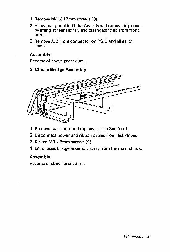
1. Remove M4 X 12mm screws (3).
2. Allow rear panel to tilt backwards and remove top cover by lifting at rear slightly and disengaging lip from front bezel.
3. Remove A.C input connector on P.S. U and all earth leads.
Assembly
Reverse of above procedure.
3. Chasis Bridge Assembly
1. Remove rear panel and top cover as in Section 1.
2. Disconnect power and ribbon cables from disk drives.
3. Siaken M3 x 6mm screws (4)
4. Lift chassis bridge assembly away from the main chasis.
Assembly
Reverse of above procedure.
Winchester 3

4. Winchester Disk Drive
1. Remove chassis bridge assembly as in Section II
2. Remove 9 x 36 unc screws (4)
3. Slide Winchester drive out.
Assembly
Reverse of above procedure.
4 Winchester
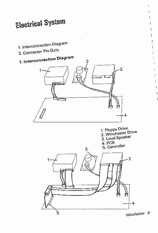
E\ectrica\ S"stem
1. interConnection Diagram
2. Connector Pin-Outs
1. InterConnection Diagram 3
II 4
1 . FlopPV Drive 2. Winchester Drive 3. Loud Speaker 4. PCB
3 5. Controller
4
5 Winchester 5
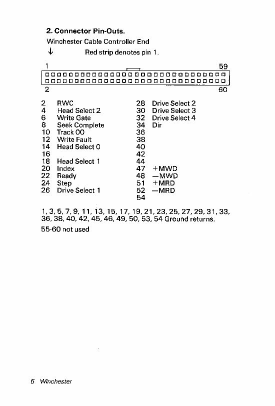
2. Connector Pin-Outs. Winchester Cable Controller End
.J, Red strip denotes pin 1.
59 000000000000000000000000000000 000000000000000000000000000000·
2 60
2 RWC 4 Head Select 2 6 Write Gate 8 Seek Complete 10 Track 00 12 Write Fault 14 Head Select 0 16 18 Head Select 1 20 Index 22 Ready 24 Step 26 Drive Select 1
28 Drive Select 2 30 Drive Select 3 32 Drive Select 4 34 Dir 36 38 40 42 44 47 +MWD 48 -MWD 51 +MRD 52 -MRD 54
1,3,5,7,9,11,13,15,17,19,21,23,25,27,29,31,33, 36, 38, 40, 42, 45, 46, 49, 50, 53, 54 Ground returns.
55-60 not used
6 Winchester
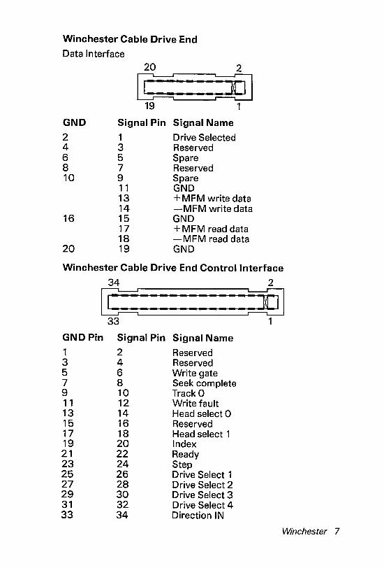
Winchester Cable Drive End
Data Interface
GND
2 4 6 8 10
16
20
20 2
~::::~ 19 1
Signal Pin
1
Signal Name
Drive Selected Reserved Spare Reserved Spare
3 5 7 9 11 13 14 15 17 18 19
GND +MFM write data -MFM write data GND + MFM read data -MFM read data GND
Winchester Cable Drive End Control Interface
34 2
~:::::::::::~ 33 1
GND Pin Signal Pin Signal Name
1 2 Reserved 3 4 Reserved 5 6 Write gate 7 8 Seek complete 9 10 Track 0 11 12 Write fault 13 14 Head select 0 15 16 Reserved 17 18 Head select 1 19 20 Index 21 22 Ready 23 24 Step 25 26 Drive Select 1 27 28 Drive Select 2 29 30 Drive Select 3 31 32 Drive Select 4 33 34 Direction IN
Winchester 7

Winchester Drive Power Cable
4 3 2 1
Co 0 0 0) Pin
1 2 3 4
Signal
+12V OV OV +5V
8 Winchester
Drive Wire Colour
Yellow Black/White Black Red
4 3 2 1
~ Signal
+5V OV OV +12V
Motherboard Wire Colour
Red Black Black/White Yellow

!Electronic Svstem
1. Outline Of Controller.
2. Integrated Circuit Catalogue
3. Mnemonics
1. Outline of Controller
Introduction
The Winchester disk drive controller is a single board expansion card which fits into either one of the system expansion slots and connected to the disk drive by a ribbon cable.
The board acts as the interface between the processing system and the Winchester disk drive.
Description
The controller is broken into seven parts; the WD 1010-05, Data seperator, write precompesation, addressing, RAM buffer control port and finally a data bus.
Winchester Disk Controller (WD1010-05)
The Winchester disk interface consists of a WD 1 0 1 0-05 and associated buffers.
The interface provides all the control functions necessary for formatting and transferring data to and from the winchester disk.
Winchester 9
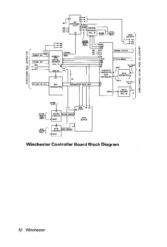
c.: 0 t-U W z: z: 0 U
'" ::::> III
z: 0 Vi z: <t c.. X W
J:j_A113 _A112 _AlII
ADIlRt:SS BUS
ClJiTR!I.. BUS
ItfT2
DATA BUS (DO -D7)
SECTOR CIlUIiTER
RESET CHBCR)
BVTE CDUlfTER
RESET
ADDRESS AND
CONTROL DECODING
EN
BUS TRANSCEIVER
DO
A113
BYTE ClUfTER
RESET HEAD
~-----------IINTRQ
~====================~~ ~-------4r---I~ ~-------r--t----I RE
WDIOIO-OS WINCHESTER
DISK CONTROLLER
DO
WINCHESTER DATA BUS v-~~~~~~~~--~n
,-.-,-----{ID7
WDATA
SELECTS
_IiSO _1iS1 _HS2
Winchester Controller Board Block Diagram
10 Winchester
£ 2 n I rTJ
'" --I rTJ ;;0
t:j
Vi A
t:j ;;0
:( rTJ
n o :z :z rTJ n --I
6 :z '"

The WD 1010-05 is selected by WCCS from PAL 1 .
Head select is controlled by the control port (IC8).
The controllers registers are selected by AB 1 - 3 from the Apricot.
Data Separator.
The DP8460 (lC2) data separator receives digital pulses from a differential line receiver which converts the data from balanced to TTL format. The data separators lock to the frequency of these input pulses and separates them into synchronized data and clock signals.
Write Precompensation
The Rodime R0350 does not require write precompensation although the controller is capable of producing early, normal and late data. Write data (WDATA) from the WD 1010-05 can be used to drive a delay line, (Not normally fitted). This generates two extra write data signals delayed by 1 Ons and 20ns. These data signals are then selected by PAL2 which is controlled by RWC/EARLY and LATE from the WD1010-05.
The write data output of PAL2 is converted to balanced format by the differential line drive.
Addressing.
The PAL 1 is used to interface the address bus from the Apricot to the Winchester controller. It receives address lines AB4-AB8 which allows the controller to detect accesses to the WD1010-05.
The control port and the data port ABO qualifies the device selects and ALE is used to prevent glitches as the addresses change.
When the WD 1010-05 isolates the local bus to perform a data transfer the PAL 1 would produce NRAMCS from the appropriate address. PAL 1 is also enabled by BCS from the WD1010-05.
The WD 1010-05 interrupt request output (INTRQ) is bufferd by PAL 1 and output as NINT2 to the Apricot.
To meet the address setup times of the WD 10 10-05, the read enable signal is delayed by qualifying it with the data enable signal whenever the controller is addressed by the Apricot Ica also adds additional wait states by holding IRDY low until its Qc output goes high. This counter is clocked by the 5MHz clock (CLK5).
Winchester 11

The expansion bus is buffered by tri-state drivers to avoid contention with other expansion cards.
Control Port
The control port (IC6) is an 8 bit addressable latch enabled by the signallatch-CK from PAL 1.
The signals HSO-HS2 are used to select the winchester head.
ClKSEl defines if the system processor or the WD 1 0 1 0-05 causes the sector pointer to be incremented.
XFERD is a handshaking protocol informing the WD 1010-05 that data is available.
HBCR is used to reset both the sector pointer and the byte pointer to zero. It is controlled by the system processor.
Data Bus
The local data bus is isolated from the expansion bus by IC5 an octal bus transceiver. Its"direction is controlled by NIORC from the Apricot and enabled by NDATAEN from PAL 1.
Static Ram.
This 8K x 8 or 2K x 8 bit buffer acts as a temporary store for all data transfers. Data is written into the buffer from the Apricot and then access is passed to the WD 1010-05 which transferes the data to the winchester disk.
RAM chip select, read enable and write enable are controlled by PAL 1.
The RAM addresses are generated by counters which form the byte pointer( IC7 + IC 1 O} and sector pointer{lC8}.
The byte counter is incremented by the byte clock from PAL 1 and goes high whenever RE or WE is active from either the CPU or WD10105.
The sector counter is clocked by sector ClK from PAl2. This is derived from either the Byte counter reaching its maximum count or from the buffer data request of the WD1010-05.
The byte counter is reset by the signal BCR from IC4. This is generated by either the system {HBCR} or the WD 1 01 0-05 (NWBCR).
The sector counter is only reset by the system {HBCR}, this is to allow for a WD 1010-05 option to be implemented.
12 Winchester
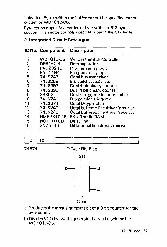
Individual Bytes within the buffer cannot be specified by the system or WD 1 0 1 0-05. Byte counter specify a particular byte within a 512 byte section. The sector counter specifies a particular 512 bytes.
2. Integrated Circuit Catalogue
IC No. Component Description
1 2 3 4 5 6 7 8 9
10 11 12 13 14 15 16
WD1010-05 DP8460-4 PAL 20210 PAL 14H4 74LS245 74LS259 74LS393 74LS393 26S02 74LS74 74LS374 74LS240 74LS240 HM6264P-15 NOT FITTED SN75116
IC 10
Winchester disk controller Data separator Program array logic Program array logic Octal bus tranceiver 8-bit addressable latch Dual 4 bit binary counter Dual 4 bit binary counter Dual retriggerable monostable D-type edge triggered Octal D-type latch Octal buffered line driver/receiver Octal buffered line driver/receiver 8K x 8 static RAM Delay line Differential line driver/receiver
74S74 D-Type Flip-Flop
Set
D Q
0:
Clear
a) Produces the most significant bit of a 9 bit counter for the byte count.
b) Divides VCO by two to generate the read clock for the WD1010-05.
Winchester 13
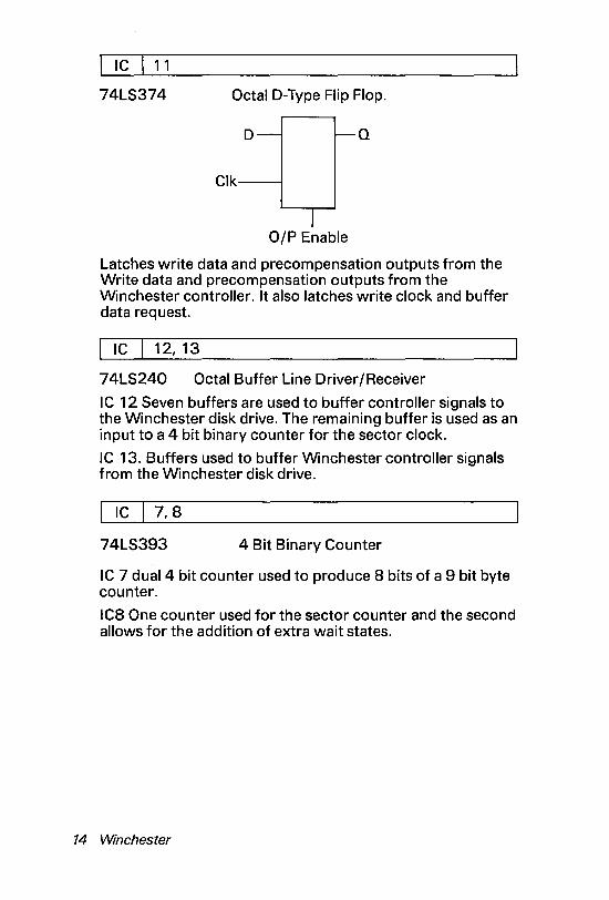
IC 11
74LS374 Octal D-Type Flip Flop.
D Q
Clk----f
D/P Enable
Latches write data and precompensation outputs from the Write data and precompensation outputs from the Winchester controller. It also latches write clock and buffer data request.
I IC I 12, 13
74LS240 Octal Buffer Line Driver/Receiver
IC 12 Seven buffers are used to buffer controller signals to the Winchester disk drive. The remaining buffer is used as an input to a 4 bit binary counter for the sector clock.
IC 13. Buffers used to buffer Winchester controller signals from the Winchester disk drive.
I IC I 7,8
74LS393 4 Bit Binary Counter
IC 7 dual 4 bit counter used to produce 8 bits of a 9 bit byte counter.
IC8 One counter used for the sector counter and the second allows for the addition of extra wait states.
14 Winchester
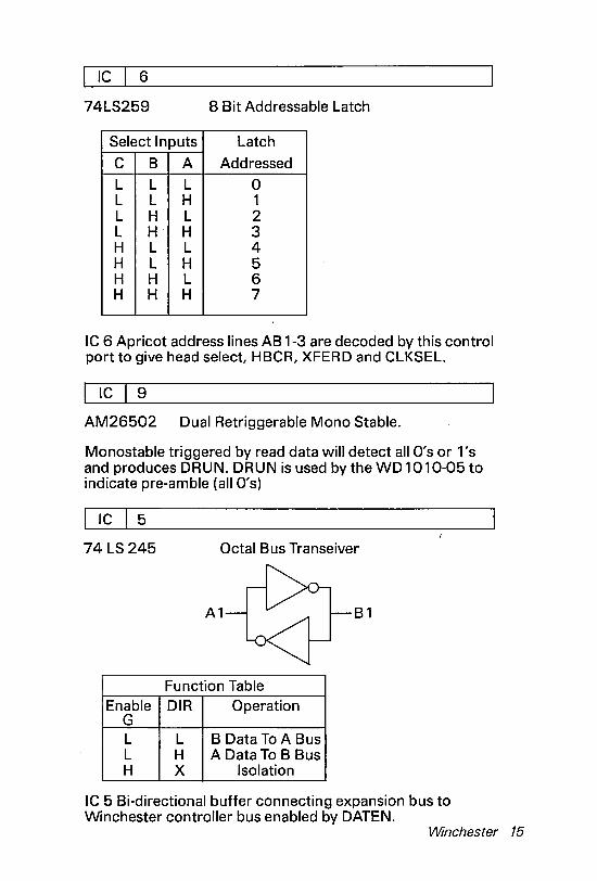
Ie 6
74LS259 8 Bit Addressable Latch
Select Inputs Latch
C B A Addressed
L L L 0 L L H 1 L H L 2 L H H 3 H L L 4 H L H 5 H H L 6 H H H 7
IC 6 Apricot address lines AB 1-3 are decoded by this control port to give head select, HBCR, XFERD and CLKSEL.
I IC 19 AM26502 Dual Retriggerable Mono Stable.
Monostable triggered by read data will detect all O's or 1 's and produces DRUN. DRUN is used by the WD 1010-05 to indicate pre-amble (all O's)
I IC I 5
74 LS 245 Octal Bus Transeiver
A1 B1
Function Table Enable DIR Operation
G L L B Data To A Bus L H A Data To B Bus H X Isolation
IC 5 Bi-directional buffer connecting expansion bus to Winchester controller bus enabled by DATEN.
Winchester 15
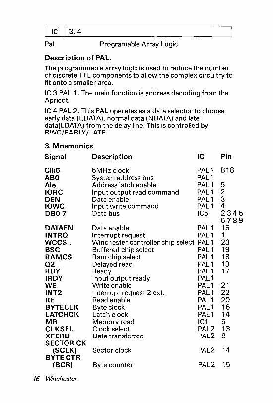
16
IC 3,4
Pal Programable Array Logic
Description of PAL.
The programmable array logic is used to reduce the number of discrete TTL components to allow the complex circuitry to fit onto a smaller area.
IC 3 PAL 1. The main function is address decoding from the Apricot.
IC 4 PAL 2. This PAL operates as a data selector to choose early data (EDATA), normal data (NDATA) and late data( LDATA) from the delay line. This is controlled by RWC/EARLY /LATE.
3. Mnemonics
Signal Description IC
Clk5 5MHz clock PAL1 ABO System address bus PAL 1 Ale Address latch enable PAL1 IORC Input output read command PAL1 DEN Data enable PAL1 IOWC Input write command PAL 1 DBO-7 Data bus IC5
DATAEN Data enable PAL1 INTRO Interrupt request PAL 1 WCCS. Winchester controller chip select PAL 1 BSC Buffered chip select PAL1 RAMCS Ram chip select PAL1 02 Delayed read PAL1 RDY Ready PAL1 IRDY Input output ready PAL1 WE Write enable PAL 1 INT2 Interrupt request 2 ext. PAL 1 RE Read enable PAL1 BYTECLK Byte clock PAL 1 LATCHCK Latch clock PAL1 MR Memory read le1 CLKSEL Clock select PAL2 XFERD Data transferred PAL2 SECTOR CK
(SCLK) Sector clock PAL2 BYTE CTR
(BCR) Byte counter PAL2
Winchester
Pin
B18
5 2 3 4 2345 6789 15 1 23 19 18 13 17
21 22 20 16 14 5 13 8
14
15
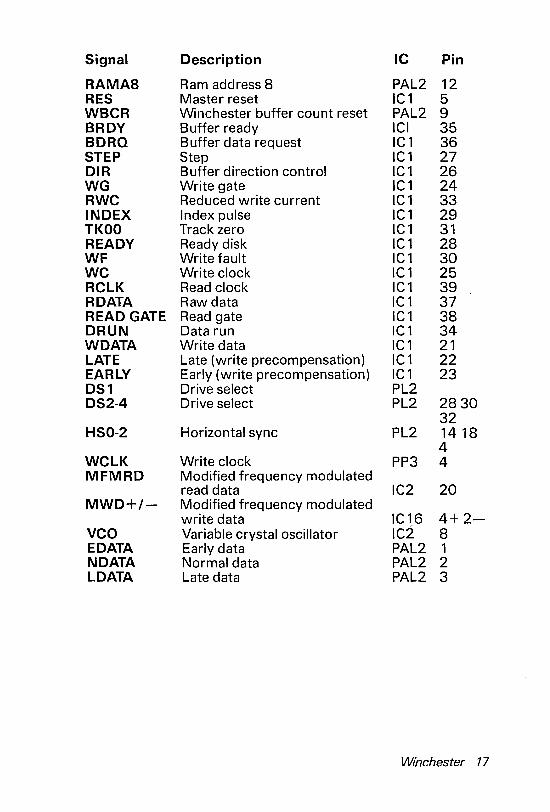
Signal Description IC Pin
RAMA8 Ram address 8 PAL2 12 RES Master reset IC 1 5 WBCR Winchester buffer count reset PAL2 9 BRDY Buffer ready ICI 35 BDRQ Buffer data request IC 1 36 STEP Step IC1 27 DIR Buffer direction control IC1 26 WG Write gate IC1 24 RWC Reduced write current IC1 33 INDEX Index pulse IC1 29 TKOO Track zero IC1 31 READY Ready disk IC1 28 WF Write fault IC1 30 WC Write clock IC1 25 RCLK Read clock IC1 39 RDATA Raw data IC1 37 READ GATE Read gate IC1 38 DRUN Data run IC1 34 WDATA Write data IC 1 21 LATE Late (write precompensation) IC1 22 EARLY Early (write precompensation) IC 1 23 DS1 Drive select PL2 DS2-4 Drive select PL2 2830
32 HSO-2 Horizontal sync PL2 14 18
4 WCLK Write clock PP3 4 MFMRD Modified frequency modulated
read data IC2 20 MWD+/- Modified frequency modulated
write data IC16 4+2-VCO Variable crystal oscillator IC2 8 EDATA Early data PAL2 1 NDATA Normal data PAL2 2 LDATA Late data PAL2 3
Winchester 17
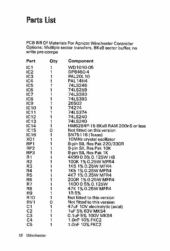
Parts list
PCB Bill Of Materials For Apricot Winchester Controller Options: Multiple sector transfers, 8Kx8 sector buffer, no write pre-compe
Part IC1 IC2 IC3 IC4 IC5 IC6 IC7 IC8 IC9 IC10 IC 11 IC12 IC13 IC14 IC15 IC16 X01 RP1 RP2 RP3 R1 R2 R3 R4 R5 R6 R7 R8 R9 R10 RV1 C1 C2 C3 C4 C5
18 Winchester
Qty
1 1 1 1 1 1 1 1 1 1 1 1 1 1 o 1 1 1 1 1 1 1 1 1 1 1 1 1 1 1 o 1 1 1 1 1
Component
WD1010-05 DP8460-4 PAL20L10 PAL 14H4 74LS245 74LS259 74LS393 74LS393 26S02 74274 74LS374 74LS240 74LS240 HM6264P-15 8Kx8 RAM 200nS or less Not fitted on this version SN75116 (Texas) 10M Hz crystal oscillator 8-pin SIL Res Pak 220/330R 8-pin SIL Res Pak 10K 8-pin SIL Res Pak 1 K 4K99 0.5% O. 125W H8 100K 1 % 0.25W MFR4 1 K5 1 % 0.25W MFR4 1 K5 1 % 0.25W MFR4 4K7 1% 0.25W MFR4 200R 1 % 0.25W MFR4 1 KOO 0.5% O. 125W 47K 1 % 0.25W MFR4 1R5% Not fitted to this version Not fitted to this version 47uF 10V electrolytic (axial) 1 uF 5% 63V MKS4 O. 1 uF 5% 100V MKS4 1.0nF 10% FKC2 1.0nF 10% FKC2
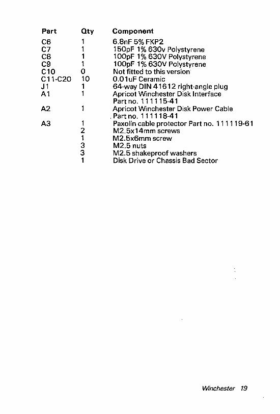
Part Qty
C6 1 C7 1 C8 1 C9 1 C10 0 C11-C20 10 J 1 1 A 1 1
A2
A3 1 2 1 3 3 1
Component
6.8nF 5% FKP2 150pF 1 % 630v Polystyrene 100pF 1 % 630V Polystyrene 100pF 1 % 630V Polystyrene Not fitted to this version 0.01 uF Ceramic 64-way DIN 41612 right-angle plug Apricot Winchester Disk Interface Part no. 111115-41 Apricot Winchester Disk Power Cable
. Part no. 111118-41 Paxolin cable protector Part no. 111119-61 M2.5x 14mm screws M2.5x6mm screw M2.5 nuts M2.5 shakeproof washers Disk Drive or Chassis Bad Sector
Winchester 19

1. Winchester Controller CCT
2. Component Layout
20 Winchester

Printed in England by Studio Press SP 10485/1 MI AT

'----MO_N_ITO_R ___ ~I ~
Service ManuTai CRT Data Display
MODEL K-907 A9 Chassis No. Y08A
CONTENTS SAFETY PRECAUTIONS ...................................................................................................................................... 1
GENERAL INFORMATIONS ................................................................................................................................ 1
CRT DATA DISPLAY SPECIFICATIONS ............................................................................................................. 2
CONNECTOR WIRING .......................................................................................................................................... 4
TIMING CHART .................................................................................................................................................... 4
BLOCK DIAGRAM ................................................................................................................................................. 5
MONITOR CIRCUIT BOARD DETAIL COMPONENT LOCATION ...................................................................... 6
CONTROL DESCRIPTION .................................................................................................................................... 7
ALIGNMENT PROCEDURE .................................................................................................................................. 8
PREASSEMBLY INSPECTION AND HANDLING INSTRUCTIONS ................................................................... 10
CAUTION FOR SERVICING ............................................................................................................................... 10
MONITOR CIRCUIT BOARD·SOLDER VIEW .................................................................................................... 11
SCHEMATIC DIAGRAM FOR K·907A9 .............................................................................................................. 12
TROUBLE SHOOTING HINTS ............................................................................................................................ 13
REPLACEMENT PARTS LIST ............................................................................................................................. 18
Panasonic@ Matsushita Electric Trading' Co., ltd. po. Box 288. Central Osaka Japan
· K-907A9
------SAFETy PRECAUTIONS------
1-1 CAUTION: No modification of any circuit should be attempted. Service work should only be performed after you are thoroughly familiar with illl of the following Silfety checks and servicing guide lines.
1-2 SAFETY CHECK Care should be taken while servicing this CRT display because of the high voltage used in the deflection cir· cu its. These voltages are exposed in such areas as the associated flyback and yoke circuits.
1-3 FIRE & SHOCK HAZARD 1-3-1 Insert an isolation transformer between the CRT
display and AC power line before servicing chassis. 1-3-2 In servicing pay attention to original lead dress
especially in the high voltage circuit. If a short circuit is found, replace all parts which have been overheated as a result of the short circuit.
1-3-3 All the protective devices must be reinstalled per original design.
1-3-4 Soldering must be inspected possible for cold solder joints, frayed leads, damaged insulation, solder splashes or sharp solder points. Be certain to remove all foreign material.
1-4 IMPLOSION PROTECTION All Panasonic picture tubes are equipped with an integral implosion protection system, but care should be taken to avoid damage and scratching during installation. Use only Panasonic replacement picture tubes.
1-5 X-RADIATION WARNING: The only potential source of X-Radiation is the picture tube. However when the high voltage circuitry is operating properly there is no possibility of X-Radiation problem. The basic precaution which must be exercised is to keep the high voltage at the following factoryrecornrnended level.
Note: It is important to use an accurate periodically calibrated high voltage meter.
1-5-1 To measure the hig!l voltage, use a high impedance high voltage meter. Connect (-) to chassis and (+) to the CRT anode button.
1-5-2 Turn tile Brightness control fully counterclockwise. 1-5-3 Measure the high Voltage. The high voltage meter
should indicate at the following factory-recommended level.
1-5-4 If the upper meter indication exceeds the rnaximum level, irnmediate service is required to prevent the possibl ity of premature component failure.
1-5-5 To prevent X-Radiation possibility, it is essential to use the specified picture tube.
1-5-6 The nominal high voltage is 11 KV and must not
exceed 14_5KVat zero beam current at rated Voltage.
,.-__ ..l INPORTANT SAFETY NOTICE '--__ ~
There are special components used in Panasonic CRT
displays which are important for safety. These parts are
identified by the international symbol & on the sche
matic diagram and on the replacement parts list. It is
essential that these critical parts should be replaced
with manufacture's specified parts to prevent X
RADIATION, shock, fire or other hazards. Do not
modify the original design without written permission
of the Panasonic company or this will void the original
parts and labor guarantee.
-----GENERAL INFORMATIONS------Here is an outline of Model K-907A9. These a model are CRT DATA DISPLAY of metal frame type. K-907A9 uses P39 (Green) phosphor and Polish Cathode Ray Tube. For improke the interlace, add High Voltage block and make stabilization of High Voltage_ Input signal is separate type and each input signal is put through 10 pin-cardedge connector on the P_C. Board.
When connecting to equipment, directly connect it to printed circuit board input terminal through 10-pin card edge connector_
Input signal is for TTL level.
In additon, +B is supplied from the outside through 10-pin card edge connector, operating the monitor on +11.8 DC.
Features: CRT is exceptionally superb in quality and reliability and is of Polish type (direct etched CRT), Phospher P39.
The deflection coil is a yoke equipped with 4-P magnet and is of PANASONIC's own design that permits adjustment of geometric distortion on the raster_
In order to meet users' requirements, frame mechanism is employed for easy adjustment of CRT setting angle.
Angle can be changed by stages such as 0°,2.5°,5°,7.5° and 10°
Chassis is fully equipped with ICs: Vertical deflection H.AFC/OSC
F.B.T is sealed up for assuring high quality and reliability_
All connections are equipped with connectors to make servicing easier.
-1-
K-907A9
----CRT DATA DISPLAY SPECIFICATIONS---
1. PHYSICAL CHARACTERISTICS
Dimension:
Height:
Width:
Depth:
Weight:
Picture Tube:
Tilt:
174mm max.
241 ±1.5 mm
226±5.0 mm
6.2 Ibs (2.B kg)
240AMB39 polish
Visual 9" 90° def. 20 mm
dia.
10° ± 1°
2. ELECTRICAL CHARACTERISTICS OF CRT DISPLAY MONITOR
Power Requirements: DC 11.BV LOA
Signal Input (cf. page 4)
Video Input Signal Requirements
Input Impedance:
Black level = 0 + 0.4
-O.OV
White level = 4 ± 1.5V
300 ohms min 40pF max.
VERTICAL INPUT SYNC SIGNAL REQUIREMENTS
Active Polarity:
Pulse Rate:
Pulse Width:
Amplitude:
Input Impedance:
Positive
71.9 Hz
158/.1s
Low = 0 + 0.4
-O.OV
High = 4 ± 1.5V
1 Kohm min. 40pF max.
-2-
HORIZONTAL INPUT SYNC SIGNAL
REQUIREMENTS
Active Polarity:
Pulse Rate:
Pulse Width:
Amplitude:
Positive
15.79 kHz
aOlls
Low = 0 + 0.4
-O.OV
High = 4 ± 1.5V
Input Impedance: 2 Kohms min. 40pF max.
Video Amplifier Band Width:
Resolution:
Character Area
Vertical:
Horizontal:
25 MHz typ
~ BOO TV Lines at center
~ 650 TV Lines at corner
120±5mm
150 ±5mm
* According to the attached timing chart
* +8 = 11.8 ± 0.05V
BLANKING TIME REQUIREMENTS
Vertical: 1200 liS min.
Horizontal: 10 liS min.
Deflection Linearity
Vertical: 10% (max - mi.n x 100)
Horizontal: 10% max + min
Raster Distortion: See Fig. 1
Centering: See Fig. 2
H. Tilt: See Fig. 3
Storage Temperature - 40 -+ 65°C
Humidity: 5 - 90% (Non·Condensing)
Altitude: o - 40,000 Feet
Operating Ambient Temperature:
0- 55°C
Humidity:
Altitude:
5 - 90% (Non-Condensing)
0-10,000 Feet
NOTE: -Be sure not to power-off within 10 seconds
after power-on to avoid spot-burn.
- SG and FG (Franme ground) are separated
by 100 K ohm resister.
K-907A9
1. Trapezoid
2, Pincushion
3, Barrelling
0'" b,
ctJ b',
r=+i 4=J
c',
4, Parallelogram
f'l~
~~f'
al,a'.1 ;:::; 2.4 mm a2,a'2;:::; 1.7 mm
a,
d a',
I I bl,b'l ;:::; 0,9 mm b2,b'2;:::; 1.2 mm b,~: i--b', D I I
CI,C'I ;;; 0,9 mm C2,C'2 <_ 1.2 mm c]
fl,h;:::; 2,0 mm
I :
Fig, 1 GEOMETRIC DISTORSION
A2
Fig, 2 CENTERING
Outline of phosphor area
Character area
IA1-A21~5mm IB1-B21~5mm
-3-
Character area
Fig,3 HOR IZONTAL TI L T
Center scan line at character area
K-907A9
-------CONNECTOR WIRING-------
P.C.B. CARD EDGE CONNECTION
1234567
Position key way insert between pins 9 and 10 from pin side.
[I]ITJ[I]rnillOJOJOJITJm (Wiring side shown)
--------TIMING CHART-------
Horizontal Sync. Timing
Vertical Sync. Timing
Sync (Positive)
Character
k ROI'S
o 63.3331'5 I'S J (15.798kHz)
II 10.01lS
I 1111111111111111111"'"1111111111 ~ O+O.4V -0
Low 0+ 0.4 V -0
High 4 ± 1.5V
High
Sync --.fl No.1 Field n No.2 Field fL +4±1.5V
(Positive) ~ I 1 J ~~;4V 0.158ms h3.902ms 13.902ms -0
~ (71.934Hz) (71.934Hz) 1.267ms
1.203m~ r12.667msl i12.667ms--j High
Character 1 111111111111111111111111 """II""I"I"III~ t;~.:v± 1.5V
Note; Time tolerance; ± 0.1% -0
Unit is adjusted according to this timing and frequency. Example:
Dot freq. : 15.000 MHz Character block : lOx 16 Total characters: 80 x 25
-4-
K-907A9
-------BLOCK DIAGRAM-------
Non r.:\ Connection ~
Supply Common Return
-5-
EHT
G4
MONITOR CIRCUIT BOARD DETAIL COMPONENT LOCATION
Side plate ------.-"I,~=!~i~~~~~~~~~t~------- CRT·
Geometric correcting magnets(4)
CRT ground spring -----,~
Centering magnets(2)-----T
Video P.C.Board ----~=::;~
..------ Anode cap
----- Deflection yoke
~_---H.out
044
~~~~---- FBT
Bleeder resistance (FBT)
FIG Ground ----j~~e~~;~~~~:~~~~~!~~~ Terminal ~
Input edge connector Bottom plate P.C.Board Holder
Rear Chassis View
V.Lin (VR33) ----~---'-_:_::.'::,....
V. Hold -------"'---:-~~~~~~mi~~~~~~~~~r'~ (VR31)
FIG Ground Terminal
V. Height (VR32)
Sub·Brightness (VR67)
Monitor Circuit Board Detail-Component Location
-6-
Focus VR (VR64)

K-907A9
------CONTROl DESCRIPTION------
Clamp
.---_______ +-VR67
~::: V.LI, ~ 1. I S,b B,;,h",,,
~~~;Id --roo T ®+-H. H,;"" .....LI'\ 1- _'" I VR64 ,,'"'
VR41 H. Hold -----t_=====~_L403 H. Width
Correcting Magnet of Geometric Distortion (4)
Main P. C. Board-Top View
Vertical Hold (VR31): Stabilizes the raster vertically.
Vertical Height (VR32): Adjusts the height of the active display area.
Vertical Linearity (VR33):
Adjusts the height of the characters within the active display area.
Horizontal Hold (VR41): VR41 can be considered a fine adjustment for the horizontal stability and position of the display area Adjust VR41 to center the display area.
Horizontal Width (L403): Adjusts the width of the active display area.
Sub Brightness (VRG7): (Internal)
Adjusts the brightness of the raster.
Brightness: (User Supply)
Adjust the brightness of the raster.
Deflection Yoke Side View
Focus (VRG4): Adjusts the focus in the center of the active display area'. Keep the whole picture uniform and then adjust it to the best point.
Tilt Adjustment (1): The tilt adjustment entails the use yoke clamp. Loosening the yoke clamp and rotating the yoke either clockwise or counter-clockwise corrects the tilt of the raster.
Centering Magnets (2):
(Located on the yoke between the yoke electrical termination and the yoke clamp.) These controls are used to center the raster vertically.
Geometric Posit,ioning Magnets (4):
-7-
(Located around the yoke periphery) adjusts the geo· metric shape of the active display area.
K-907A9
------ALIGNMENT PROCEDURE------
PREPARATION 1. Connect the 10·Pin connector from the proper logic to
the defined input signal. 2. Apply power to the CRT data display and allow the
monitor to stabilize. 3. Adjust coils by means of a hexagonal tuning tool (non
metalic). Variable resister by - screw driver and deflection yoke (deflection distortion) by square tuning tool {non· metalicl.
4. All controls are set at optimum position prior to shipment.
ADJUSTMENT PROCEDURE • Image Tilt Adjustment
Loosen the deflection yoke clamp and turn in the arrow directions to adjust tilt. (See Fig. 4).
Incorrect Correct
\ I
r :' __ _ ~ ' ___ .character area f-I
"-,
Fig. 4
• Vertical Hold Adjustment Adjust (VR31) until the image becomes stable vertically as shown in Fig. 5.
Rolling
M _____________ M I
M
M----~------- M
Locking in
Fig. 5
-8-
Checking of height, width and bright should be performed more than 30 minutes after power is applied. Measure the luminous intensity near the center of CRT and set at 50 Lx ±20% (40 to 60 Lx). These adjustment are performed on the basis of the input signal of timing chart (page 4).
• Horizontal Hold Adjustment
Adjust the VR41 to get stable character (syncroning condition) as shown in below (See Fig. 6). Under the condition of free running i. e. horizontal sync signal is disconnected.
Bad Good Bad
Fig. 6
• Vertical Height Adjustment Adjust the vertical height (V R32) to set the vertical height of the active character area as shown in Fig. 8.
-rl--I-=-Incorrect Vertical height
t------+--I~- Correct Vertical height
Fig. 8
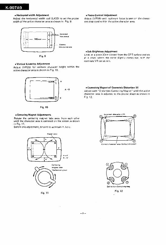
K-907A9
• Horizontal width Adjustment Adjust the horizontal width coil (L403) to set the proper width of the active character area as shown in Fig. 9.
160mm
Fig. 9
• Vertical Linearity Adjustment
Incorrect
Horizontal
Correct
HOrizontal size
Adjust (VR33) for uniform character height within the active character area as shown in Fig. 10.
Fig. 10
• Centering Magnet Adjustments
Rotate the centering magnet tabs away from each other until the character area is centered on the screen as shown
·in Fig. 11. Before this adjustment. be sure to ascertain H. hold.
Raster area
Fig. 11
• Focus Control Adjustment Adjust (VR64) until optimum focus is seen on the characters displayed within the active character area.
• Sub Brightness Adjustment Look at a place 30cm distant from the CRT surface and set at a point where the raster slightly comes out. with the contrasts VR set at min .
• Correcting Magnet of Geometric Distortion (4)
Adjust each "Distortion Correcting Magnet" until the active character area is adjusted to the proper shape as shown in Fig. 12.
Correct character area IDefiection yoke)
Deflection Correcting mag
Fig. 12
-9-
K-907A9
--- PREASSEMBLY INSPECTION AND HANDLING INSTRUCTIONS
Caution: Be sure all handling of the CRT Display is done by the CRT mounting brackets. At no time should the wires be used as a means of moving or carrying a given CRT Display. The CRT neck is the most fragile part of the CRT Display Module and extreme care should be taken not to bump, tap, or otherwise excert force on this neck. Before applying power to the CRT Display an inspection should be preformed to insure that any foreign material has not been dropped in any part of the CRT Display. i. Insure that the proper signal and power connections are
made in accordance.
2. Apply power to CRT display under test and allow CRT display to stabilize for a minimum of 5 minutes.
Note: All adjustments have made at the factory. This procedure is to insure that these adjustments have been made correctly.
3. When turn External Brightness Control to max imum and raster should be slightly visible.
4. Check CRT display for proper centering. 5. Check CRT display for the specified active character area
per Page 2 of this Manual.
6. Check Geometric Distortion. 7. Check focus. S. Check Power Supply Voltages in accordance per Page 2
of this Manual.
----- CAUTION FOR SERVICING ------Be sure to provide power supply sequence of more than lOOms.
Power ON-OFF
00 not turn OFF- power supply when the CRT heater is not sufficiently heated. Otherwise, CRT may be burned in spot.
In case of servicing or replacing CRT, high voltage sometimes remains in the anode of CRT. So, completely discharge high voltage before servicing or replacing CRT so as to prevent a shock to the serviceman. In this case, discharge to thr external conductive coating (aquadag) of CRT.
-10-
Discharging to other places will cause troubles. The heat sink of horizontal output transistor is applied with +B. So, do not earth it in case of servicing.
In case of storaging or transporting it, be sure to take some countermeasures for static electricity. When using a soldering iron, be sure to connect it to the earth.
The unused terminal should be soldered without fail.
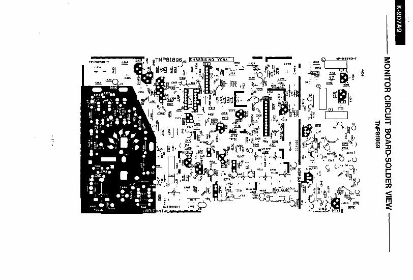
s: o z =i o ::xJ o 35 o c:
-t =i z "tJ Cl
~~ m ::xJ
C I en o r C m ::xJ < iii :E
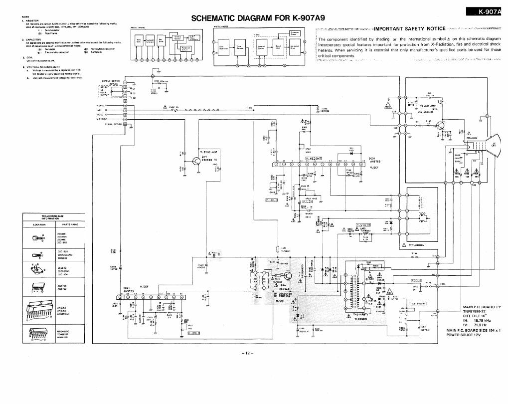
NOTE
1. RESISTOR SCHEMATIC DIAGRAM FOR K-907A9 All reliston8111 carbon 1/4W resillor, unless olherwis.e nOled the following marks. Unit 01 resistance il OHM (n). (1<-1,000, M-l,OOO,oOO)
Solid resistor 0: Non Flame
2. CAPACITOR All capacitors ere ceramic SOV cap/ICitor, unless otherwil8 noted the following markl. Unit of ceP/ICitance il "F. unlel$ otherwise noted.
(QI: Polyester !F: Electrolyliccapac;itor
J. COIL Unit of inductance il"H.
4. VOLTAGE MEASUREMENT a. Voluge is menured by a digital meter wilh
DC 10Mn OHM/V receiving normallignal.
b. Use each menUlement voltage lor reference.
@: PoJYltylenecapacitor (!l: Tantalum ~"""" v.", .... 00'" "'. OU'PU' ~~:::"'~.
csc c ...... o 0 ....
P.o,,,,.on c .. ,u"
, 1 l • S & 1 e g '0 " 11
R R702100K\\W
C702 oon 1630\11
VIDEO cr eo
;:F~~~SI~~~ASE
LOCATION PARTS NAME
Q);;a!"© 2SC828 2SC829C 2SC945
~ 2SC1318
c:n-~ 2SC1825 2SCI360ANC
• 2SC2532
~o 2SC940
2SC901ilN 2SCll54
fiiiiiiiI AN5753 AN5752 <D ___ I)
~ AN5762 AN5763
ANS76JINJ
©
fiiW· MP04011C TC40118P MN40118 <D ____ rn
RI61 2.2K
Cl61 16VlO
J401 2.2K
~!
~~ ,
IC" 03 AN5753"
H.DEF
[, " ... ,. o 3 ,e 1 a 9
V.SYNC.AMP
QI7 2SC8n "
'0
... r-
C~ll
16\1330 -
., ....• F
-12 -
."~ ., .~ §~-~R3\ e" IOOXII7 7 9 ~
iV.HO,"oi E: <r:
~ The component identified by shading or the international symbol ..t on this schematic diagram incorporates special features important for protection from X-Radiation, fire and electrical shock
zfi C10~ ,);,e\l12oo
0' i~:HE!.GHll
_16Vn VRJJIOXe 1
+ IV.LINi
10V470
Cl'O
it is essential that only manufacturer's specified parts be used for those
I
IC31 AN57e3
V.DEF
!8~lQI8]
Lt~%&~~IO
""~+ oa:"t
ili
\IRS?
IOQKB
,
R151 8101' ..
~ OYTLYS033i1A
/l10t ",'
,r. '"
~ R~ 7~ .. ,
VRU
'"
(0,,1>
MAIN P.C. BOARO TY ,-----€J------' TNP81S96-32
CRT TILT 10· tH: 15.79 kHz tV: 71.9 Hz
MAIN P.C. BOARD SIZE 194 xl POWER SOUCE 12V
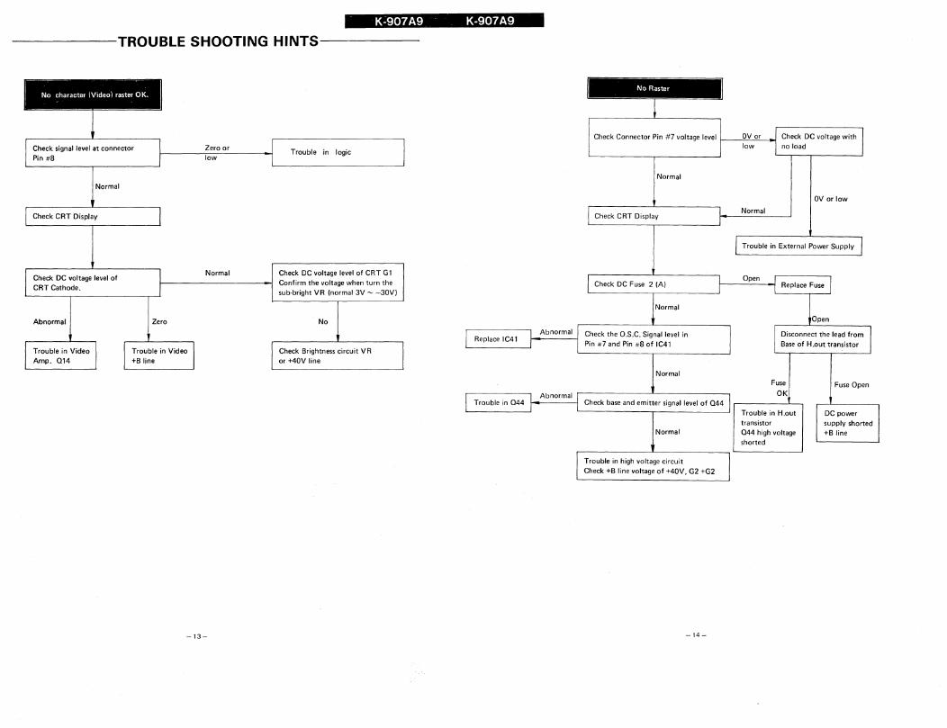
K-907 A9 K-907 A9
-----TROUBlE SHOOTING HINTS-----
Check signal level at connector Pin #8
Normal
Check CRT Display
Check DC voltage level of CRT Cathode.
Abnormal
Trouble in Video Amp. 014
Zero
Trouble in Video
+B '-ine
Zero or low
Normal
-13-
Trouble in logic
Check DC voltage level of CRT G1 Confirm the voltage when turn the sub·bright VR (normal 3V - -30VI
No
Check Brightness circuit VR or +40V line
Check Connector Pin #7 voltage level r--~-'--'''-----i Check DC voltage with no load
Normal
Check CRT Display
Check DC Fuse 2 (AI
Normal
Check the O.S.C. Signal level in Pin # 7 and Pin #8 of IC41
Normal
Check base and emitter signal level of 044
Normal
Trouble in high voltage circuit Check +B line voltage of +40V. G2 +G2
-14 -
OV or low
Normal
Trouble in External Power Supply
Fuse OK
Trouble in H.out transistor Q44 high voltage shorted
Fuse Open
DC power
supply shorted +8 line
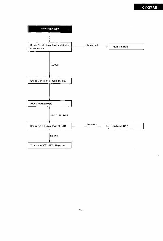
No vertical sync . .
Check Pin #9 signal level and timing of connector
Normal
Check Verticalty of CRT Display
Adjust Vertical hold
No vertical sync
Check Pin #1 signal level of IC31
Normal
Trouble in IC31 (IC31 Replace)
K-907A9
Abnormal Trouble in logic
Abnormal Trouble in Q17
-15-
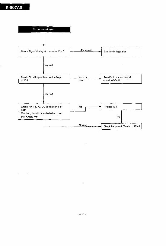
K-907A9
No horizontal sync
Check Signal timing at connector Pin 6
Normal
Check Pin #3 signal level and voltage of IC41
Normal
Check Pin #4, #9, DC voltage level of IC41 Confirm, should be varied when turn the H.Hold VR
Abnormal
Zero or low
No
Normal
-16-
Trouble in logic side
Trouble in the peripreral circuit of C401
Replace IC41
No
Check Peripreral Ci.rcuit of IC 41
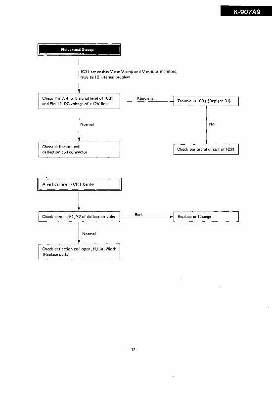
No vertical Sweep
IC31 are cosists V.osc V.amp and V output therefore, may be IC internal problem
K-907A9
Check Pin 2,4,5,8 signal level of IC31 and Pin 12, DC voltage of +12V line
Abnormal Trouble in IC31 (Replace 31)
Normal
Check deflection coil deflection coil connector
II A vertical line in CRT Center
No
Check peripreral circuit of IC31
1\
I Check contact Pl, P2 of deflection yoke Jf----s""ae..:d:..:·-------II Replace or Change
Normal
I Check deflection coil open, H.lin, Width I (Replace parts)
-17-
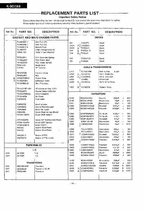
-K-907A9
-----REPlACEMENT PARTS lIST-----Important Safety Notice
Components identified by the international symbol&' have special characteristics important for safety. When replacing any of these components use orily manufacturer's specified parts.
Ref. No. PART NO. DESCRIPTION Ref. No. PART NO. DESCRIPTION
CABINET AND MAIN CHASSIS PARTS DIODES
TUWB1967·1 Side Plate (R) D31 TVS10El Diode TUWBI96B-l Side Plate (L) D43A Lt TVSBB4A Diode TUX80B47-5 Bottom Plate D43B Lt TVSBB4A Diode TUX80721 (High Voltage) Bracket D44 Lt TVS2DL15 Diode TBMBll04 Model (Plate) K907A9 D46 .1:. TVSBB4 Diode
TESB1B9-1 CRT Grounded Spring D47 TVSSI R20 Diode TKXB22001 PCB Holder (Big)
D51 TVSBB4 Diode TKXB22101 PCB Holder (Small)
TMM1455 Beads Band
TJC341 lP Terminal COILS & TRANSFORMERS
TMK81526 L141 TLT047-999 Peaking Coil 4.7~H
I nsulator Sheet
TMMB1457 L403 Lt TLHB0710 Horiz. Width Coil
Nut
Lt 240AMB39MD Picture Tube L404 Lt TLHB0619 Horiz. LIN. Coil
L405 TLP40B Choke Coil Lt TLYB0339A Deflection Yoke
TN PB1B96-32 Main PCB Assy. L430 Lt TLHB0410 Horiz. Drive Trans.
TXAJTV4P179A 4P Connector Assy. (DY) T401 Lt TLFBOB79 Flyback Trans.
TPCB26071 (Outer) Carton K907A9
TXAPD2M900Z Filler Complete CAPACITORS TPEB14056 Set Cover
TOFB0525 Fuse Label C143 ECCDI H221J Ceramic 220pF J
C145 ECEA1JS100 Electrolytic lO~F -
TOFB0759 Warning Label C161 ECEA1CS100 Electrolytic lO~F -
TOF80B02 Service Warning Label C302 ECOM1Hl03JZ Polyester O.Ol~F J
TOFB3825 Serial No. Label C303 ECOM1H472JZ Polyester 4700pF J
XSN4+BS Screw (High Voltage Block)
XTV3+15BFN Screw (PCB Holder) C304 ECSF35ER33V Tantalum O.33~F -C305 ECSF16E4R7Y Tantalum 4.7~F -
XTV3+BBFN Screw (1 P Terminal Side Plate) C306 ECSF 16E4R7Y Tantalum 4.7~F -
XTB4+10AFN Screw (CRT Spring) C307 ECEA1CS100 Electrolytic lO~F -XTB4+20BFN Screw (CRT) C30B ECEAOJS330 Electrolytic 33~F -XWA4B Washer (Side Plate)
XWA3B Washer (Side Plate) C309 ECEA1CS221 Electrolytic 220~F -C310 ECEA1AS471 Electrolytic 470~F -
XWG5H14 Washer (CRT) C311 ECOM1H333JZ Polyester O.033~F J
XWC3BFN Washer (1 P Terminal) C312 ECEA1CS471 Electrolytic 470~F -C401 ECOM1HI83JZ Polyester O.OlB~F J
TNP81896-32 C402 ECOM1H153JZ Polyester O.015~F J
C403 ECOM1Hl03JZ Polyester O.OI~F J
I.C C404 ECEA1ES4R7 Electrolytic 4.7~F -IC31 AN5763 I,e C405 ECOS1392JWT Styrol 3900pF J
IC41 AN5753 I.C C406 ECOM1Hl02JZ Polyester 1000pF J
C423 ECEA1CS331 Electrolytic 330~F -TRANSISTORS C430 ECOM1Hl53JZ Polyester O.OI5~F J
014 2SC1360ANC Transistor C441 ECKD2Hl02KB2 Ceramic 1000pF K
017 2SCB2BAR Transistor (a, R) C442 Lt ECOM4223KZ Polyester O.022~F K
044 2SC901BN Transistor C443 Lt ECOM4223KZ Polyester O.022~F K
-IB-
50V
63V
16V
50V
50V
35V
16V
16V
16V
6.3V
16V
10V
50V
16V
50V
50V
50V
25V
IOOV
50V
16V
50V
500V
400V
400V
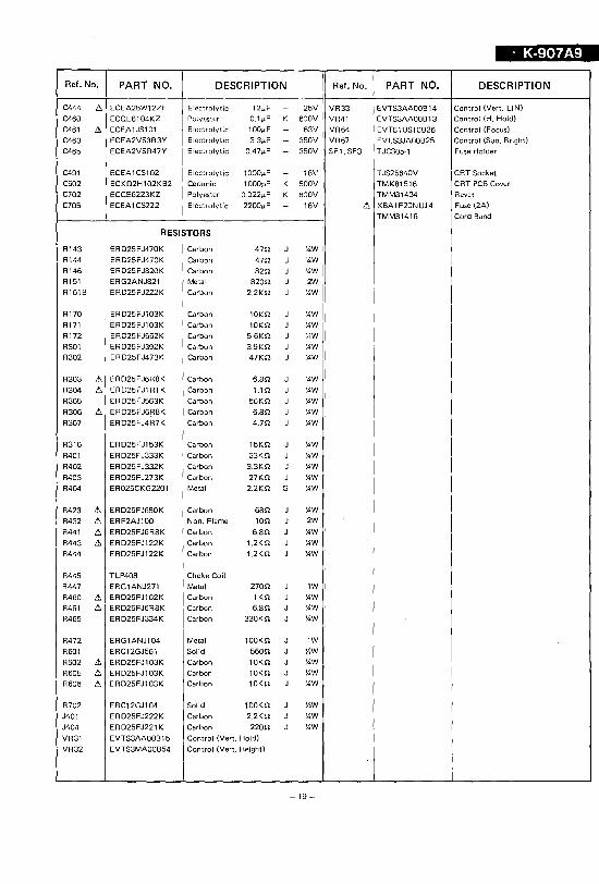
o K-907A9 .
Ref. No. PART NO. DESCRIPTION Ref. No. PART NO. DESCRIPTION
C444 & ECEA25W12ZE Electrolytic 12"F - 25V VR33 EVTS3AAOOB14 Control (Vert. LIN)
C460 ECOE6104KZ Polyester O.Ij.LF K 600V VR41 EVTS3AAOOB 13 Control (H. Hold)
C461 & ECEA1JS10l Electrolytic 100j.LF - 63V VR64 EVTS1US10B26 Control (Focus)
C463 ECEA2VS3R3Y Electrolytic 3.3j.LF - 350V VR67 EVLS3JAOOB25 Control (Sub. Bright)
C465 ECEA2VSR47Y Electrolytic O.47j.LF - 350V SFI. SF3 T JC305·1 Fuse Holder
C491 ECEA1CS102 Electrolytic 1000j.LF - 16\' TJS25640V CRT Socket
C602 ECKD2Hl02KB2 Ceramic 1000pF K 500V TMK81516 CRT PCB Cover
C702 ECOE6223KZ Polyester O.022j.LF K 600V TMM81434 Revet
C705 ECEA1CS222 Electrolytic 2200j.LF - 16V & XBA 1 F20NU.14 Fuse (2A)
TMM81416 Cord Band
RESISTORS
R143 ERD25FJ470K Carbon 47n J YOW R144 ERD25FJ470K Carbon 47n J YOW R146 ERD25FJ820K Carbon 82n J YOW R151 ERG2ANJ821 Metal 820n J 2W
R161B ERD25FJ222K Carbon 2.2Kn J YOW
R170 ERD25FJ103K Carbon 10Kn J YOW R171 ERD25FJ103K Carbon 10Kn J YOW Rl72 ERD25FJ562K Carbon 5.6Kn J YOW R301 ERD25FJ392K Carbon 3.9Kn J YOW R302 ERD25FJ473K Carbon 47Kn J YOW
R303 & ERD25FJ6RSK Carbon 6.Sn J YOW R304 & ERD25FJ1R1K Carbon 1.1n J YOW R305 ERD25FJ563K Carbon 56Kn J YOW R306 & ERD25FJ6f1SK Carbon 6.Sn J YOW R307 ERD25FJ4R7K Carbon 4.7n J YOW
R310 ERD25FJ153K Carbon 15Kn J YOW R401 ERD25FJ333K Carbon 33Kn J YOW R402 ERD25FJ332K Carbon 3.3Kn J YOW R403 ERD25FJ273K Carbon 27Kn J YOW R404 E R025C KG2201 Metal 2.2Kn G YOW
R423 & ERD25FJ680K Carbon 6Sn J YOW R432 & ERF2AJ100 Non. Flame Ion J 2W
R441 & ERD25FJ6RSK Carbon 6.Sn J YOW R443 & ERD25FJ122K Carbon 1.2Kn J YOW R444 ERD25FJ122K Carbon 1.2Kn J YOW
R445 TLP40S Choke Coil
R447 ERG1ANJ271 Metal 270n J lW
R460 & ERD25FJ102K Carbon lKn J YOW R461 & ERD25FJ6RSK Carbon 6.Sn J YOW R465 ERD25FJ334K Carbon 330Kn J YOW
R472 ERG1.ANJ104 Metal 100Kn J lW
R601 ERC12GJ561 Solid 560n J YOW
R602 & ERD25FJ103K Carbon 10Kn J YOW R605 & ERD25FJ103K Carbon 10Kn J '!.W
R606 & ERD25FJ103K Carbon 10Kn J '!.W
R702 ERC12GJ104 Solid 100Kn J YOW
J401 ERD25FJ222K Carbon 2.2Kn J '!.W
J404 ERD25FJ221 K Carbon 220n J '!.W
VR31 EVTS3AAOOB 15 Control (Vert. Hold)
VR32 EVTS3MAOOB54 Control (Vert. Height)
-19-

I· DISK DRIVE 1 ~
MICRO FLOPPYDISK DRIVE OA-D32W ---O-A---O-3-2-V-····
·SONY SERVICE MANUAL
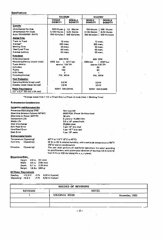
Specifications
Capacity
Unformatted Per Disk Unformatted Per Track Bu~tTRANSFER RATE
AccessTlma
Track to Track Average-Settling Time Head load Time Average latency
Functional
Rotational Speed Recording Density (inside track) Track density Cylinde~
Tracks R/W Heads Encoding Method
Heat Dissipation
Operating Mode (Head load) Standby mode (Head Unload)
Media Requirements 3.5" x 3.7" (90 mm x 94 mm)
OA·D32W
SINGLE I DOUBLE DENSITY DENSITY
500 Kbytes /1.0 Mbytes 3.125 Kbytes 6.25 Kbytes 250 Kbits/sec 500 Kblts/sec
12 msec. 350 msec.
30 msec. 60 msec. 50 msec.
600 RPM 4359 bpi I 8717 bpi
approx. 135 TPI 80
160 2
FM, MFM
6.0W 3.9W
SONY OM·D4440
OA·D32V
SINGLE I DOUBLE DENSITY DENSITY
250 Kbytes /500 Kbytes 3.125 Kbytes 6.25 Kbytes 250 Kblu/sec 500 Kblts/sec
12 msec. 350 msec. 30msec. 60 msec. 50 msec.
600 RPM 4094 bpi I 8187 bpi
approx.135 TP I 80 80
1 FM, MFM
6.0W 3.9W
SONY OM·D3440
-Average access time - 1/3 x (Track Nos.) x (Track to track time) + (Settling Time)
Environmentel Considerations
ReliabilitY and Maintainability Preventive Maintenance (PM) Meantime Between Failures (MTBF) Meantime to Repair (MTTR) Component life Media life Disk Interchange Soft Read Error Hard Read Error Seek Error
Environmental limits
Temperature (Operating) Humidity (Operating)
Vibration (OpeFatlng)
Dim'Mional Data Height Width Depth Weight
2.0 In. (51 mm) 4.0 in. (102 mm) 5.1 in. (130 mm) 1.51bs (650 g)
DC Power Requirements
Not required 8000 POH (Power On Hourtime) 30 min. 5 years or 15,000 POH 3.0 x 10" passes/traek 20,000 times 1 per 10' bits read 1 per 10" bits read 1 per 10" seeks
40· F to 115°F (5·C to 45·C) 20 % to 80 % relative humidity, with a wet bulb temperature of 85· F (29·C) and no condensation. The unit shall perform all read/write operations (no seek) according to specifications, with continuous vibration of less than 0.5 G (± 1 0 %) from 5 Hz to 100 Hz (along the x, y, z plane).
Reading +12.0 V ±5 % (Operating) +5.0 V ±5 %
0.30 A (typical) 0.48 A (typical)
RECORD OF REVISIONS
REVISION NOTES
1 ORIGINAL ISSUE
-2-
November, 1983
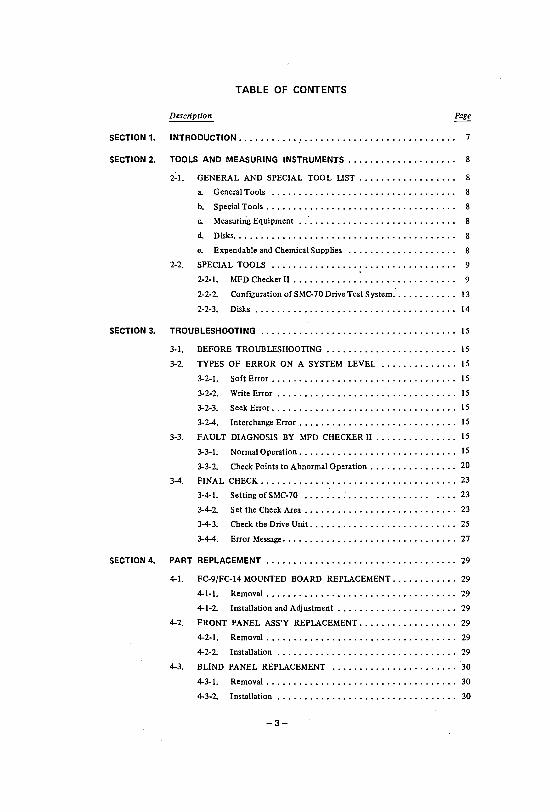
TABLE OF CONTENTS
Description
SECTION 1. INTRODUCTION . .... , ..... , . . . . . . . . . . . . . .. . . . . . . . . . . . .. 7
SECTION 2. TOOLS AND MEASURING INSTRUMENT.S ................... .
2-1. GENERAL AND SPECIAL TOOL UST . . . •. . . . • . . . . . • . .. 8
a. General Tools .....•..•..••....••.•.•......•.... 8
b. Special Tools ..••.•.••..•.....•..••.•.....••....
c. Measuririg Equipment .• ' ..•... " ..........•.........
d. Disks ...•..............•........•........•...•
e. Expendable and Chemical Supplies ...........•........
2·2. SPECIAL TOOLS ...........•.......••........ ' •... , 9
2-2-1. MFD Checker II . . . . . . . . . . . . . . . . . . . . . . . . . . . . .. 9
2-2-2. Configuration of SMC-70 Drive Test System.' . . . . . . . . . .. 13
2-2-3. Disks.. . • . . . . . • . . . . . • . • • • . . . . . . . • . . . . . . . .. 14
SECTION 3. TROUBLESHOOTING .. .................................. 15
3-1. BEFORE TROUBLESHOOTING •...•....•............. , 15
3-2. TYPES OF ERROR ON A SYSTEM LEVEL .............• 15
3-2-1. Soft Error ...............•..•..............• 15
3-2-2. Write Error ........•...........•..•...... : .. 15
3-2-3. Seek Error. . . . • . . . . . . . . • . . . . . • . . . . . • . . . . . . .. IS
3-2-4. Interchange Error. . . • . . . . . • . . . . . . . . • . . . . . . . . •. IS
3-3. FAULT DIAGNOSIS BY MFD CHECKER II ............... 15
3-3-1. Normal Operation ....•..•..................... IS
3-3-2. Check Points to Abnormal Operation ... '. • . . . . . . . . • .. 20
3-4. FINAL CHECK. . . • . . . . . • . . . . . . . . . . . . • . . . . . . . . . . . .. 23
3-4-1. Setting of SMC-70 ..•..............•..... • ... 23
3-4-2. Set the Check Area ..••.•....................•. 23
3-4-3. Check the Drive Unit. . • • . • . . • . . • . . . . . . . . • . . • . .. 25
3-4-4. Error Message .••.•........•..•.....•.....•. : . 27
SECTION 4. PART REPLACEMENT ................................... 29
4-1. FC-9/FC-14 MOUNTED BOARD REPLACEMENT ............ 29
4-1-1. Removal ....•........•........•.•...•..•... 29
4-1-2. Installation and Adjustment .•......•..........•. , 29
4-2. FRONT PANEL ASS'Y REPLACEMENT ....•.......•.... , 29
4-2-1. Removal .•..•.....•..•.....•............... 29
4-2-2. Installation................................. 29
4-3. BLIND PANEL REPLACEMENT ..•..•.....•..•.....•.. 30
4-3-1. Removal............................... . . •. 30
4-3-2. Installation................................. 30
-3-
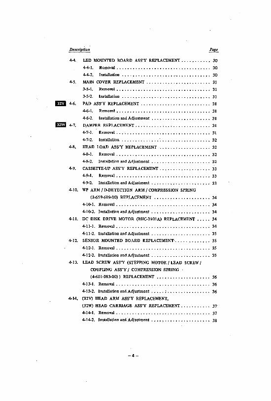
Description
4-4. LED MOUNTED BOARD ASS'Y REPLACEMENT. • • • • . . • . .• 30
4-4-1. Removal................... • • • • . . . • . . • • . • •• 30
4-4-2. Installation................. • . •• • • • . • • • • • • •• 30
4-5. MAIN COVER REPLACEMENT •••.••..•..••.••.•..••.• 31
3-5-1. Removal .••••••••..•..••••••••••..••••.•••• 31
3-5-2. Installation,................................ 31
E!D 4-6. PAD ASS'Y REPLACEMENT .•.••.•.••..•..••.••.••.•• 31
4-6-1. Removal ••.••.•..•••••.••..•....••....•..•. 31
4-6-2. Installation and Adjustment . . . • . . • . . • . . • • . • . • • • •• 31
_ 4-7. D.AMPER REPLACEMENT. . • . . . . . • • . • . • • . . • . . . . . . • . .• 31
4-7-1. Removal .•• ~ .••••.•••....••.•..•..••..••... 31
4-7-2. Installation ..•..•.....•.• '. . • • • • • . . . • • . . . • . .• 32
4-8. HEAD LOAD ASS'Y REPLACEMENT ..•...•..•.•..••.•• 32
4-8-1. Removal... . • . . • . . • . . . • • . . . . . . . . . • . . • • . • • .• 32
4-8-2. Installation and Adjustment . . . . . • . . . . . . . . . . . . • • .. 32
4-9. CASSETTE-UP ASS'Y REPLACEMENT. . • • . • . . • • . • . . • . . •. 33
4-9-1. Removal •••••..••••..•..••••..•.••..•.••..• 33
4-9-2. Installation and Adjustment • . • . • . . • • . . . . • . . • • • • •• 33
4-10. WP ARM I D-DETECTION ARM I COMPRESSION SPRING
(3-659-609-00) REPLACEMENT •••.••...•.•••••.•... 34
4-10-1. Removal •••••••••••..•.••.•...•.......••..• 34
4-10-2. Installation and Adjustment •.•..•.•••.••••••••••• 34
4-11. DC DISK DRIVE MOTOR (BHC-2101A) REPLACEMENT .••.• 34
4-11-1. Removal ••.••.••••.•...•.......•...•..••.•• 34
4-11-2. Installation and Adjustment ....••..•....••.•..•.. 35
4-12. SENSOR MOUNTED BOARD REPLACEMENT; ..•..•.••••.• 35
4-12-1. Removal................................... 35
4-12-2. Installation and Adjustment . . • • . • . . . . . • • • • • • . • • •• 35
4-13. LEAD SCREW ASS'Y (STEPPING MOTOR I LEAD SCREW I COUPUNG ASS'Y I COMPRESSION SPRING
(4-601-083-00» REPLACEMENT •..•.•.....•..•..•.. 36
4-13-1. Removal .•••.••••.••.•..•..•.••..•..•..•••• 36
4-13-2. Installation and Adjustment .•••. : ..••.••.••.•..•. 36
4-14. (32V) HEAD ARM ASS'Y REPLACEMENT.
(32W) HEAD CARRIAGE ASS'Y REPLACEMENT. . • . • • . . • .• 37
4-14-1. Removal ..•..•..••.•.•••.•..•••••.••••••••• 37
4-14-2. Installation and Adjustment •••. ~ .••.••..•••..••.• 38
-4-
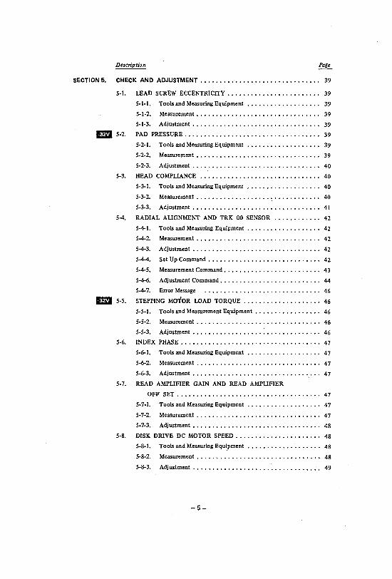
Description
SECTION 5. CHECK AND ADJUSTMENT. . . . . . . . .. . . . . . . . . . . . . . . . . . . . .. 39
5-1. LEAD SCREW ECCENTRICITY. • • • • . • • . • • . . • • • • . . • . . •• 39
5-1-1. Tools and Measuring Equipment ••. • . • • . . . • • • . . • • .• 39
5-1-2. Measurement ..•••••.•••.••.•.•••.•...•.•..•. 39
5-1-3. Adjustment ••.••..•..•••••.•.••.•••.•.••.... 39
ED 5-2. PAD PRESSURE. • • . • • • • . . • • . • • • • • . . • . • . • • • . • . . • . .• 39
5-2-1. Tools and Measuring Equipment . • • • • • . • • . . • • • • . • •. 39
5-2-2. Measurement................................ 39
5-2-3. Adjustment................................. 40
5-3. HEAD COMPliANCE .•••.•••••.•.••..••..•••..•.... 40
5-3-1. Tools and Measuring Equipment, •.•.•..•..• : ...••. 40
5-3-2. Measurement ..••••.•••••...•..• : • . • • . . • . . . .• 40
5-3-3. Adjustment................................. 41
5-4. RADIAL AliGNMENT AND TRK 00 SENSOR ...•••••..•. 42
5-4-1. Tools and Measuring Equipment ••.••.••..•....••.. 42
5-4-2. Measurement... • • • • . • • • . • . • . • • . • . . . . • . • . . . •. 42
5-4-3. Adjustment •.•••.•...•.•.•....•.....•.•..... 42
5-4-4. Set Up Command ••....••....•...•...•....•... 42
5-4-5. Measurement Command. . • . • • . . • . . • . . . . . . . . . . . •• 43
5-4-6. Adjustment Command. • . • . . • . . • . . • . . . . • . . . • . . .. 44
5-4-7. Error Message ..•..•..•.•...••..•.•..•..•.•• 46
_ 5-5. STEPPING MOTOR LOAD TORQUE . . . . . . . . • • . . . . . • . . •• 46
5-5-1. Tools and Measurement Equipment • . . . • . . . . • . . • • • •• 46
5-5-2. Measurement................ • . . • . • • • . • • . • • .• 46
5-5-3. Adjustment .•..•..•..••.•..•• :.............. 46
5-6. INDEX PHASE . • . • • • . . . . . . • . • . . • . . • • . • • . . • • • • . . . •• 47
5-6-1. Tools and Measuring Equipment •..•..••.•..•.....• 47
5-6-2. Measurement ...•.....••.•..•.••..••.•...•.•• 47
5-6-3. Adjustment •..•..............•..•..•..•• "- • .. 47
5-7. READ AMPliFIER GAIN AND READ AMPUFIER
OFF SET .••..••.•.....••.•..•.•••.•..•..•..•. 47
5-7-1. Tools and Measuring Equipment ...•....•.••..•...• 47
5-7-2. Measurement •..•...•...••....•.•••..••••••.. 47
5-7-3. Adjustment................................. 48
5-8. DISK DRIVE DC· MOTOR SPEED. . . . . • . • • . • • • • • • • • • • •• 48
5-8-1. Tools and Measuring Equipment ..•.•.•...•........ 48
5-8-2. Measurement. • . • . . . . . • . . • • . . . . • . . • • . • • • • . . .. 48
5-8-3. Adjustment.................... .. • . . . . . • . . . .• 49
-5-
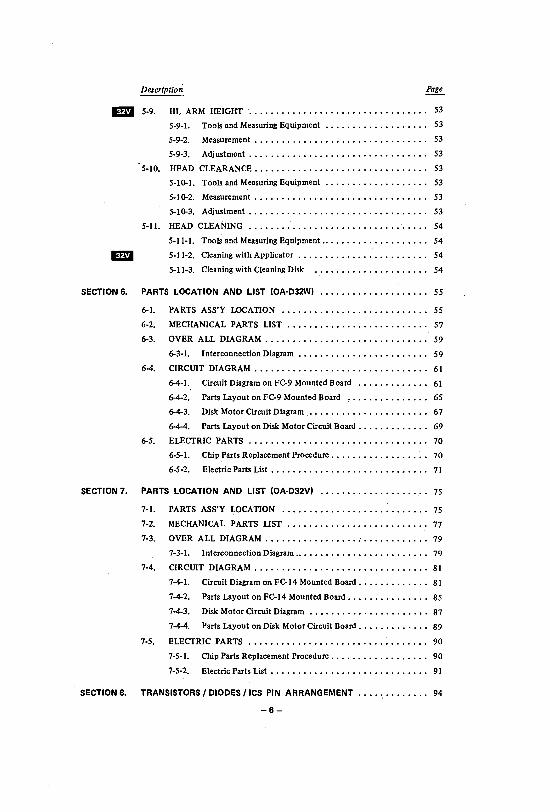
Description
_ 5-9. HL ARM HEIGHT ...•..•..••.••.•••.•••••••••••... 53
5-9-1. Tools and Measuring Equipment •••••.••....•..•... 53
5-9-2. Measurement...... • . • • • • . • • • • . • . • . . • • . . • . • •. 53
5-9-3. Adjustment................................. 53
5-10. HEAD CLEARANCE. . • • . • . . . . • • • . . • • . • • • • . • • . . • • . .. 53
5-10-1. Tools and Measuring Equipment .•••••..•.•••••...• 53
5-10-2. Measurement................................ 53
5-10-3. Adjustment................................. 53
5-11. HEAD CLEANING ...•.... " .•..•..••.•..•..••.•.•••. 54
5-11-1. Tools and Measuring Equipment .....•.••.••••••••.. 54
_ 5-11-2. Cleaning with Applicator . • . • . . . • . . • • . . . • . . . • . . •. 54
5-11-3. Cleaning with Cleaning Disk •.•......•.•••••.•••• 54
SECTION 6. PARTS LOCATION AND LIST (OA·D32W) ••••••.•..•••••••••• 55
6-1. PARTS ASS'Y LOCATION ..•..•..•.•..•..•••.••••••• 55
6-2. MECHANICAL PARTS LIST .••.••..•..•.••..•..•..... 57
6-3. OVER ALL DIAGRAM . . • . . • . • . . . • • . • . . • . . • • • • • . • • •• 59
6-3-1. Interconnection Diagram . . . • • • • • • . . • • • . • . • • • . • •. 59
6-4. CIRCUIT DIAGRAM . . • . • . . • • . • • . . . • . . . • • . • • . • • . • • .. 61
6-4-1. Circuit Diagram on FC-9 Mounted Board ••.•..•••.••• 61
6-4-2. Parts Layout on FC-9 Mounted Board ..•..•..••.•..• 65
6-4-3. Disk Motor Circuit Diagram ••••.••.••• . • . • . • • . . .• 67
6-4-4. Parts Layout on Disk Motor Circuit Board. • . • • . • • . • . •. 69
6-5. ELECTRIC PARTS .•.••••••• ; ••..•.•..••..•..•..••. 70
6-5-1. ChipParts Replacement Procedure. • • . • • . • • . • • • • • . •• 70
6-5-2. Electric Parts List • • . . . . • . • • • • . • . . . • • . • • . •• . • •. 71
SECTION 7. PARTS LOCATION AND LIST (OA·D32V) ••.••••••••••.•••.•• 75
7-1. PARTS ASS'Y LOCATION ..•.••••••...•••...•••.••.• 75
7-2. MECHANICAL PARTS LIST .•.•••.•.••..••.••••..•.•• 77
7-3. OVER ALL DIAGRAM ................... ; • • . • . . . . . •. 79
7-3-1. Interconnection Diagram .••••••.••..••.•.••.•...• 79
7-4. CIRCUIT DIAGRAM . • . • . . • . • . . • . • • . • • • • • . • . • • . . • • .. 81
7-4-1. Circuit Diagram on FC-14 Mounted Board ••.••••.....• 81
7-4-2. Parts Layout on FC-14 Mounted Board ..••••..•..•.•• 85
7-4-3. Disk Motor Circuit Diagram .• • • • • • . • • . • • . • • . • • . •. 87
7-4-4. Parts Layout on Disk Motor Circuit Board. • . • • • • • . • • .• 89
7-5. ELECTRIC PARTS .•.••.•••.••••.••..•..••.•••••.•. 90
7-5-1. Chip Parts Replacement Procedure .••• ; • • . • . . • . . • • .• 90
7-5-2. Electric Parts List • • . • . . . . . • • • • • . • • . • • . • . . • . . •. 91
SECTION 8. TRANSISTORS I DIODES IICS PIN ARRANGEMENT .• • . • . • • • . • .. 94
-6-
SECTION 1
INTRODUCTION
I ntroauctlc
This manual is a maintenance guide for OA-D32W (Double sided) and OA-D32V (Single sided).
The overall check after removals and adjustments will be included in this section.
SECfION 2 describes disks and tools necessary for maintenance.
SECfION 3 provides fault diagnostic procedures that may require spare parts or some adjustments.
SECfION 4 and 5 cover parts replacements and adjustments, respectively.
SECfION 6 and 7 consist of circuit diagrams, ass'y drawin~s, and parts lists.
The cassette dummy (4-603-929-00) should be inserted in the OA-D32W when it is transported. Otherwise, its heads may be damaged.
Perform maintenance in accordance with the procedure specified in this manual as follows:
(Example)
e. Fasten the guide shaft with the two screws (PSW2.6 x 6).
lED f. Fasten the head board to the chassis on the bottom surface, and apply nut lock paint to the screw.
ED g. Connect the head board to the head harness (by four points) with a soldering iron. (Refer to Fig. 4-14 (c) )
Em h. Connect the head board to the head harness (by six points) with a soldering iron. (Refer to Fig. 4-14 (d) )
Em i. Fasten head board and terminal shield plate with a screw (PSW2.6 x 8) on the chassis bottm, and then apply nut lock paint onto it.
Em j. Perform the stepping motor load torque adjustment. (Refer to 5-5)
k. Install the cassette-up ass'y in place. (Refer to 4-9)
Steps e, h, i, and k should be carried out in sequence for the OA-D32W. Steps e, f, g, j and k should be carried out in sequence for the OA-D32V.
-7-
jenera) ana :special 1001 List
SECTION 2
TOOLS AND MEASURING INSTRUMENTS
·1. GENERAL AND SPECIAL TOOL LIST
The tools, and measuring instruments for performing laintenance on the OA-D32W/OA-D32V are listed below.
General Tools
TOTSU Screw Driver (M2.6)
@ Driver 2 mm
e Driver 2 mm
e Driver 4 mm
Tweezers
Round Nose Plier
Adj Rod
Cutter
Soldering Iron (20W)
Desoldering Metal Braid
SONY Parts No.
(7-721:-050-62)
(7-700-749-01)
(7-700-750-01)
(7-700-750-04)
(7-700-753-02)
(7-700-757-01)
(7-700-733-01)
(7-700-758-02)
DC Power Supplier (+5 V DC ±5 %, 0.8 A max., +12 V DC±S %,1.5 A max.)
Tester
Special Tools
MFD Checker IT
SMC-70 System
(J-609-182-0A)
SMI-70111 SMI-701IA I SMI-70121 SMI-7012A
SMC-70
KX-13GI
AID Converter
25P/26P Conversion Cable
Radial Alignment System Disk
(OR-D86VA)
(J-623-o02-oA)
(J-623-901-0A)
(8-960-009-74)
Error Check.system Disk (OR-D87VA)(8-960-009-7S)
Rotatory Knob (fOt Stepping Motor) (J-609-o11-0A)
Lead Screw Eccentricity Inspection Tool (J-609-136-oA)
Standard Disk Dummy (for Cassette-Up Ass'y Installation)
Geared Driver
Pad Weight
Hexagon Wrench Torque Driver
Power Cable
Interface Cable
(J-609-120-0A)
(J-609-0 17-0A)
(J-609-124-0A)
(J-609-125-0A)
(J-609-130-0A)
(J-609-200-0A)
c. Measuring Equipment
Oscilloscope Dual Trace 20 MHz
Universal Counter Resolution 0.1 msec.
Tension Gauge (Max. 200 g)
Tension Gauge (Max. 20 g)
d. Disks .
Level Disk
ED OR-D46VA
Em OR-D46WA
Alignment Disk
ED OR-D47VA
Em OR-D47WA
Dynamic Inspection Disk +30
ED OR-DSIVA
Em OR-D5IWA
Dynamic Inspection Disk -30
ED OR-D52VA
Em OR-D52WA
Cleaning Disk
ED OR-D29VA
Em OR-D29WA
e. Expendable and Chemical Supplies
Nut Lock Paint
Alcohol
Sony Oil
Sony Grease
Bamboo Stick
Applicator
~8-
(J-6 04-1 63-OA)
(7-732-o50-fO)
(8-960-009-31)
(8-960-009-40)
(8-960-009-32)
(8-960-009-41)
(8-960-009-35)
(8-960-009-44)
(8-960-009-36)
(8-960-009-45)
(8-960-009-1S)
(8-960-009-39)
(7-611-0.18-01)
(7-622-001-S2)
2·2. SPECIAL TOOLS
2·2·1. MFD Checker n (1) MFD Checker n configuration
Main Checker Board I/F Cable (26pin and 34pin) Power Cable (2 pieces) Conversion Board (26pins·to-34pins)
NOTE: The Conversion Board and 34pin IfF Cable are required for the OA·D33W/OA·D33V.
(2) Micro Floppydisk Drive Connection (Refer to Fig. 2·1)
(3) MFD Checker n function switches STEP IN •....... Steps the head inwards. STEP OUT ....... Steps the head outwards.
The head continously moves if the switch is kept pressed.
SIDE SELECT .... Selects one of two heads (side 0 or side 1) for a double sided. (This switch is invalid for single sided versions.)
WRITE ... , ....•. Records, data specified by the OSC SEL switch, onto one track.
OSC SEL ........ Selects such write data as "2F", "I F", "WCP" (worst case pattern), or EXT.
Power Cable
~peClal 1001
WCP W/M .....••. Selects upper and lower patterns when the OSC SEL switch is set to WCP. (Refer to Fig. 3·3 (c), (d»
HD LOAD ....... This is used to set the plunger solenoid active.
M,OTOR ON ...•.. This is used to operate the Disk Motor.
DRIVE SELECT ... Selects the disk drive. The DRIVE SELECT switch on the disk drive relates to the DRIVE SELECT switch on the checker as follows:
Drive Checker IS101) 1 2
1 OFF OFF 2 ON OFF 3 OFF ON 4 ON ON
CHGRST ........ Resets the DSKCHG signal.
600/300 SELECT (Located in the middle of the board) .•..•..•.. Set the 600/300 SELECT
switch at "600" for the OA·D32W /OA-D32V. 80/70 SELECT (Located in the middle of the board) ..•.....•. Set the 80/70 SELECT
switch to "80" for the OA-D32W /OA-D32V.
Fig. 2-1 Drawing of Connection Between Disk Drive and MFD Checker II
-9-
~IClI IUUI5
(4) INDICATOR OSC SEL (Four LEDs in the left of the board) • • . . . . . . . . . . . . '. They indicate the selected
position on the OSC SEL switch. IfF signals (Five LEDs in the middle of the board) ......•... They indicate at the states
of TRK 00, WRTPRT, RDY, DSKCHG, and INDEX, respectively. The TRK 00, WRTPRT, RDY, and DSKCHG indicators are lit when the respective IfF signals are low (true). The INDEX indicator blinks when the INDEX signal is applied to the board.
TRACK POSITION (Seven segment LED indi-cator in the right of the board) ... , ....... .
Indicates the current track position.
(5) Test Points TP-l; ';'CM=O=T""'O=R-O=N TP-2; WRT GATE TP-3; RD DATA TP-5; INDEX TN>; STEP TP-7; ~H;:D-L"'"'O:::-A""D:::-
The GND terminal: is marked by "GND".
D DO TUCKPOSITlOtl o 9 0 0 0 0 0 0 0 LED'O LEDO'
2F we' [ll ~TRICOO WRTPRT Rev DSKCHCi INOU '0 '0 I .. POWERIN ~ 60~p~OO ~~A:KS RaJ 0-0- " .. , C3 XI []
8 + + RU.. .. R3-4~
'.> . * r-. * r-. * ~ *..-----, c:k CI L--..J L--..J R2 L---J ~ C4 T ~ ~RDDATA
C2 lei ~ Ie2 cr: Ie3 IC4q;o D=. ... I- u r£I ..... '" 0_,.. f"I • .,.."',.. ..... OTPJ
• * (:=J * ~; c=J ; C]*-c=J ; 3; ~:§:fr~ ~
~ Ie7 ,-... Rle o-ICB -4" 0- Ies..... -.tI-CI7 TPG
;o~ • c. ~0O-: • '2' C6 "2. C7 0 NN m~~* (:=J * c=J * ~ * c=J * ~ * ~ * ~Ho~:~ CE~~: 7 Iel2 ..... ~ 0-ICI3 -II-,........ Q:ICI4 ~~. """b'!=sICO- ~16 -II- ............. c}!' Iel' SOTP6
~ ZO g;. ca'-' .All CSI"-t!> .RU CIO"-t!). A51 e'l. us el2 CI:t-1i> .. JNDEX
: ;:~~%*t:::==] *~ *~ *.t:::==] *~ *t:::==] *C::=J 0'" ~ . TO~
~o I~~: ~C2C teZI Ie22 0 Ie23 ]e24 )C2S
~ 0:... '30 ~ ,~ '~O' ~ o. :W: MFD CHECKER II Q-
D~ []' Q l 0; c,9"09 Df]?rnD O:D~:D::D'" . 9 D~~~ 'oU,~o DO'" $,gE M"::O. 0:: ~~ 9E :'M 9 W W 9:
TPG t=:==t TP9 ~L[CT SELECT ON LOAO "" CHGRST L.P.IN oJ k .. WRITE OSC SEL ST[P IN STEP OUT
MFD Checker II Block Diagram
-10"":
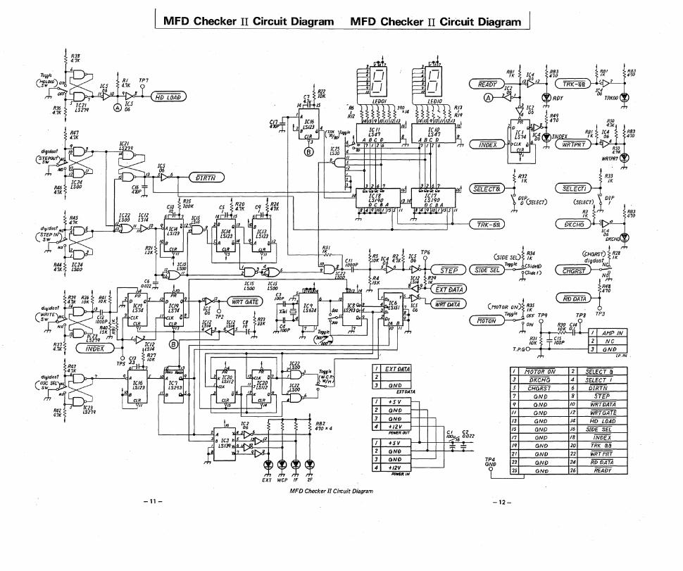
R38 0I7K
-11-
MFD Checker II Circuit Diagram MFD Checker II Circuit Diagram
~R3Z ~R33 IK IK
S£LECT& SELECTI
IDJP(SELECT) IDIP (SELEcT) 1
R3 RB3 IK 470
TRK-&& IC4 06 DKCH
RSI IK TP6
(slOE SEL)! 1:4 (CHGRST) j RZB di9dost IK
T"9g le CSideB) ( CHGRST~ ( SlOE SEL ">lCSide t)
~-t 470
RDDATA R3S IK OFF TP9 TP8 TP3
R31 10K
T.P.G
I MOTOR ON 2 SELECT & 3 DKCHa 4 SELECT I 5 CHaRST 6 DIRTN 7 aND 8 STEP
1 +S v t- 9 GND 10 WRTDATA 2 GND t-t- /I GND 12 WRTaATE 3 aNO t-t-t- 13 aND 14 HD LOAD 4 +IZV
POweR OUT CI C2
I +SV I~ 0.022
2 GNO *~
IS GND 16 SIDE SEL
17 GND 18 INDEX 19 GND 20 TRK ('J.('J.
21 GND 22 WRTPRT 3 GND r----4 +lZ-V
TP4 23 GND 24 RO DATA GND 25 GN£) 26 READY
EXT WCP IF ZF
MFD Checker II Circuit Diagram
-12-
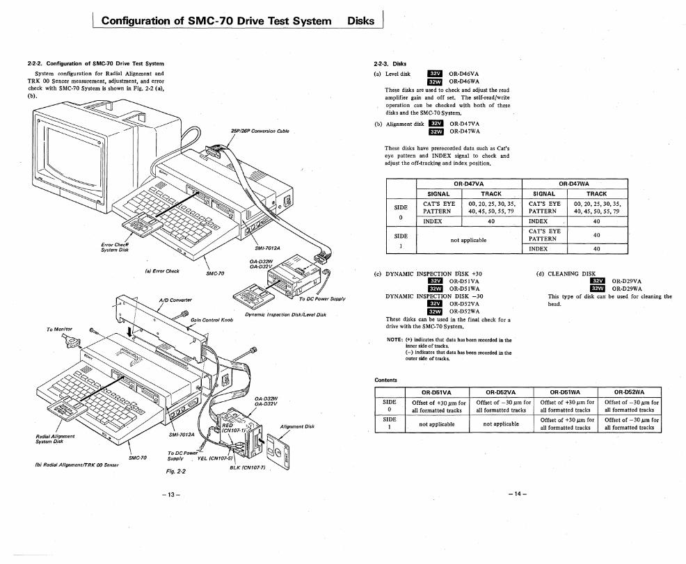
Configuration of SMC-70 Drive Test System
2·2·2. Configuration of SMC·70 Drive Test System
System configuration for Radial Alignment and TRK 00 Seneer measurement, adjustment, and error check with SMC· 70 System is shown in Fig. 2·2 (a), (b).
25P/26P Conversion Cable
(a) Error Check SMC·70
Dynamic Inspection Disk/Level Disk
To Monitor
Alignment Disk
(b) Radial AlignmentffRK 00 Senser
To DC Powe" ~'~ , Supply YEL (CNI0l·5) a Fig. 2.2 BLK (CNI0l·l)
-13-
Disks
2·2·3. Disks
(0) Level disk ED OR-D46VA _ OR-D46WA
These disks are used to check and adjust the read amplifier gain and off set. The self-read/write operation can be checked with both of these disks and the SMC-70 System.
(b) Alignment disk ED OR-D47VA _ OR-D47WA
These disks have prerecorded data such as eat's eye pattern and INDEX signal to check and adjust the off-tracking and index position.
OR·D47VA
SIGNAL TRACK
SIDE CAT'S EYE 00,20,25,30,35, PATTERN 40,45, 50, 55, 79
0 INDEX 40
SIDE not applicable
I
(c) DYNAMIC INSPECTION DISK +30 IEPl!.I OR-Q5IVA _ OR-D5IWA
DYNAMIC INSPECTION DISK -30 ED OR-D52VA _ OR-DS2WA
These disks can be used in the final check for a drive with the SMC-70 System.
NOTE: (+) indicates that data has been recorded in the inner side of tracks.
Contents
(-) indicates that data has been recorded in the outer side of tracks.
OR-D51VA OR·D52VA
OR·D47WA
SIGNAL TRACK
CAT'S EYE 00,20,25,30,35, PATTERN 40,45, 50, 55, 79
INDEX 40
CAT'S EYE 40
PATTERN
INDEX 40
(d) CLEANING DISK IEPl!.I OR-D29VA _ OR-D29WA
This type of disk can be used for cleaning the head.
OR·D51WA OR·D52WA
SIDE Offset of +30 /.1m for Offset of - 30 /.1m for Offset of +30 /.1m for Offset of -30 /.1m for 0 all formatted tracks all formatted tracks all formatted tracks ail formatted tracks
SIDE Offset of +30 /.1m for Offset of - 30 /.1m for I not applicable not applicable
all formatted tracks all formatted tracks
-14-
Before Troubleshootir
SECTION 3
TROUBLESHOOTING
SECfION 3 describes the methods of troubleshooting. 3-2 refers to several errors specfied in a system level. 3-3 describes normal operations and the check points for abnormal operations. These descriptions define the Error Spot under operating conditions.
3-1. BEFORE TROUBLE SHOOTING
The following procedures are recommended to see if the drive is really faulty or not:
I) Incorrect operational procedure
2) program error of host system
3) Poor connection with host system (esp. GNDrelated connection, frame GND, etc.)
4) Defective disk. Check that same trouble occurs with other disks.
5) Environmental conditions (where electrical noise easily jUIr.PS into signal)
6) Influence of strong magnetic field
7) Wrong supply voltage
3-2. TYPES OF ERROR ON A SYSTEM LEVEL
3-2-1. Soft Error
Soft error are caused by;
1) Dirty head
2) Electrical noise
3) Tracking error
4) Poor connection with system (GND-related connection)
5) Incorrect motor speed
6) Incorrect head compliance
Clean the head first. Check for index pulse interval and head compliance and then read error spot more than several times. If not readable, move the head to the adjacent track in the same direction as before, then return to the desired track, and read. If readable this time, check radial alignment. (Refer to 5-4) If not readable yet, the error is not recoverable.
-15-
3-2-2. Write Error
To determine whether the disk or the drive is failing, the disk should be replaced by other disks and check that there still exists write error. If write error does not exist any more, remove the old one. If write error exists with use of any ciisk, drive might cause write error.
3-2·3. Seek Error
Seek error comes from:
1) Head movement is incorrect because ellectrical noise jumps into signal.
2) Head driving system might be at fault. If it is not re-readable after re-calibration, drive might be at fault.
3-2-4. Interchange Error
If data written on one drive is readable correctly on another drive, but not by other drives, interchange error exists.
Interchange errors are caused by;
1) Head is not properly positioned.
2) Motor speed is not correct.
3) Optimum head output level and offset and head compliance are not obtained.
4) Chucking mechanism does not work.
3-3. FAULT DIAGNOSIS BY MFD CHECKER n 3-3-1 describes check method for normal
operations in accordance with the predetermined procedures.
3-3-2 describes check points for abnormal operations which come out in accordance with the above procedures.
3-3-1. Normal Operation
Pre-setting: 1) Refering to Fig. 2-1 (Micro Floppydisk Drive
Connection), connect the drive to MFD Checker
II.
2) Set the slide switch (S 101) on the disk drive to "I".
3) Set all switches in the MFD Checker II to "OFF".
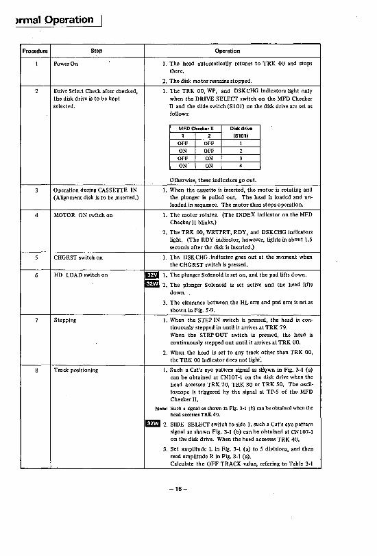
lrmal· Operation
Procedure Step Operation
1 Power On I. The head automatically returns to TRK 00 and stops there.
2. The disk motor remains stopped.
2 Drive Select Check after checked, 1. The TRK 00, WP, and DSKCHG indicators light only the disk drive is to be kept when the DRIVE SELECT switch on the MFD Checker selected. D and the slide switch (S I 01) on the disk drive are set as
follows:
MFD Checker n Disk drive
1 2 (S101)
OFF OFF 1
ON OFF 2
OFF ON 3 ON ON 4
~therwise, these indicators go out.
3 Operation during CASSETTE IN 1. When the cassette is inserted, the motor is rotating and (Alignment disk is to be inserted.) the plunger is pulled out. The head is loaded and un-
loaded in sequence. The motor then stops operation.
4 MOTOR ON switch on 1. The motor rotates. (The INDEX indicator on the MFD Checker II blinks.)
2. The TRK 00, WRTPRT, RDY, and DSKCHG indicators light. (The RDY indicator, however, lights in about 1.5 seconds after the disk is inserted.)
5 CHGRST switch on 1. The DSK CHG. indicator goes out at the moment when the CHG RST switch is pressed.
6 HD LOAD switch on mJ 1. The plunger Solenoid is set on, and the pad lifts down.
ED 2. The plunger Solenoid is set active and the head lifts down.
3. The clearance between the HL arm and pad arm is set as shown in Fig. 5-9.
7 Stepping 1. When the STEP IN switch is pressed, the head is con-tinuously stepped in until it arrives at TRK 79. When the STEP OUT switch is pressed, the head is continuously stepped out until it arrives at TRK 00.
2. When the head is set to any track other than TRK 00, the TRK 00 indicator does not lighf.
8 Track positioning 1. Such a Cat's eye pattern signal as sliQwn in Fig. 3-1 (a) can be obtained at CNI07-1 on the disk drive when the head accesses TRK 20, TRK 30 or TRK 50. The oscil-loscope is triggered by the signal at TP-5 of the MFD Checker II.
Note: Such a signal as shown in Fig. 3·1 (b) can be obtained when the head accesses TRK 40.
B 2. SIDE SELECT switch to side 1. such a Cat's eye pattern signal as shown Fig. 3-1 (b) can be obtained at CNI07-1 on the disk drive. When the head accesses TRK 40.
3. Set amplitude L in Fig. 3-1 (a) to 5 divisions, and then read amplitude R in Fig. 3-1 (a). Calculate the OFF TRACK value, refering to Table 3-1
-16-
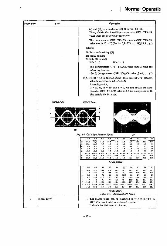
Procedure Step
9 Motor speed
(a)
Normal Operati(J
Operation
(c) and (d), in accordance with R in Fig. 3-1 (a). Then, obtain the humidity~ompensated OFF TRACK value from the following expression:
The compensated OFF TRACK value = OFF TRACK value + 0.2 (50 - II) (39.S - 0.187SN - I.SS)/33.S ... ( 1)
Where;
H: Relative humidity (%) N: Track number S: Side ID number
Side 0: 0 Side 1: 1
The compensated OFF TRACK value should meet the following formula. . -20 ~ Compensated OFF TRACK value ~ +20 •.. (2)
[EX] For R = 4.5 in the OA-D32V, the apparent OFF TRACK value is as shown in table 3-1 (d). Assuming = 4.S, H = 60 %, N = 40,aI!d S = I, we can obtain the compensated OFF TRACK value as 2.6 from expression (1). This satisfy the formula.
Fig. 3·1 Cat's Eye Pattern Signal (b)
0.0 0.1 0.2 0.3 0.4 0.5 0.6 0.7 0.8 0.9
2: 34.5 32.9 31.3 29.8 28.3 26.8 25.4 24.0 22.7 21.4 3: 20.1 18.9 17.7 16.5 15.3 14.2 13.1 12.0 11.0 9.9 4: 8.9 8.0 7.0 6.1 5.1 4.2 3.4 2.5 1.6 0.8 5: 0.0 -0.8 -1.6 -2.3 -3.1 -3.8 -4.6 -5.3 -6.0 -6.6 6: -7.3 -8.0 -8.6 -9.3 -9.9 -10.5 -11.1 -II .• -12.3 -12.9 7: -13.4 -14.0 -14.5 -15.1 -15.6 -16.1 -16.6 -17.1 -17.6 -18.1 8: -18.6 -19.0 -19.5 -20.0 -20.4 -20.9 -21.3 -21.7 -22.2 -22.6 9: -23.0 -23.4 -23.8 -24.2 -24.6 -25.0 -25.4 -25.7 -26.1 -26.5
(e) OA·D32W
0.0 0.1 0.2 0.3 0.4 Q,1 0.6 0.7 0.8 0.9
2: 36.9 35.1 33.4 31.8 30.2 28.7 27.2 25.7 24.3 22.9 3: 21.5 20.2 18.9 17.6 16.4 15.2 14.0 12.9 11.7 10.6 1: 9.6 8.5 7.5 6.5 5.5 ~ 3.6 2.7 1.8 0.9 5: 0.0 -0.9 -1.7 -2.5 -3.3 -4.1 -4.9 -5.6 -6.4 -7.1 6: -7.8 -8.5 -9.2 -9.9 -10.6 -11.2 -11.9 -12.5 -13.1 -13.7 7: -14.3 -14.9 -15.5 -16.1 -16.6 -17.2 -17.7 -18.3 -18.8 -19.3 8: -19.8 -20.4 -20.8 -21.3 -21.8 -22.3 -22.8 -23.2 -23.7 -24.1 9: -24.6 -25.0 -25.4 -25.9 -26.3 -26.7 -27.1 -27.5 -27.9 -28.3
(d) OA·D32V
Table 3·1. Apparent off Track
I. The Motor speed can be measured at TRK3S,in TP-S on MFD Checker II with an universal counter. It should be 100 msec ± 1.5 msec.
-17-
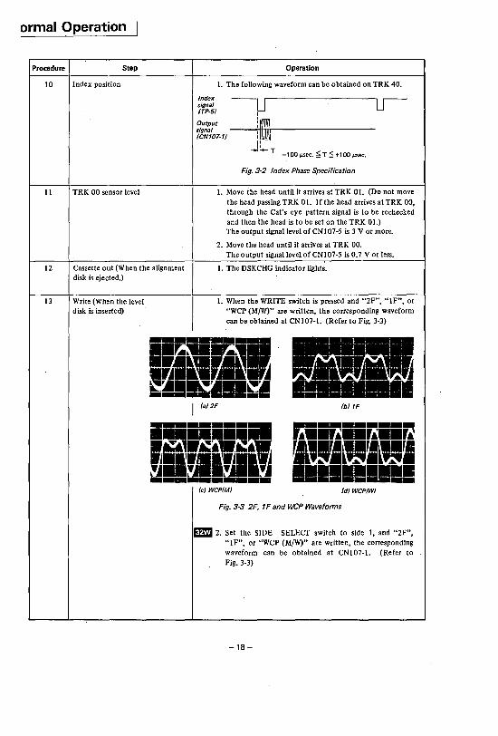
ormal· Operation
Procedure Step
10 Index position
11
12
13
TRK 00 sensor level
Cassette out (When the alignment disk is ejected.)
Write (When the level disk is inserted)
Index signal (TP-5)
Operation
1. The following waveform can be obtained on TRK 40.
I
Output signal (CN707-tJ 11
-100 "sec. ~ T ~ +100 "sec.
Fig. 3-2 Index Phase Specification
1. Move the head until it arrives at TRK 01. (Do not move the head passing TRK 01. If the head arrives at TRK 00, through the Cat's eye pattern signal is to be rechecked and then the head is to be set on the TRK 01.) The output signal level of CN I 07-5 is 3 V or more.
2. Move the head until it arrives at TRK 00. The output signal level of CNI07-5 is 0.7 V or less.
1. The DSKCHG indicator lights.
1. When the WRITE switch is pressed and "2F", "IF", or "WCP (MfW)" are written, the corresponding waveform can be obtained at CN I 07-1. (Refer to Fig. 3-3)
I (a)2F
(e) WCP(M) (d)WCP(W)
Fig. 3·3 2F, 1 F and WCP Waveforms
EE 2. Set the SIDE SELECT switch to side I, and "2F", "IF", or "WCP (MfW)" are written, the corresponding waveform can be obtained at CNI07-1. (Refer to Fig. 3-3)
-18-
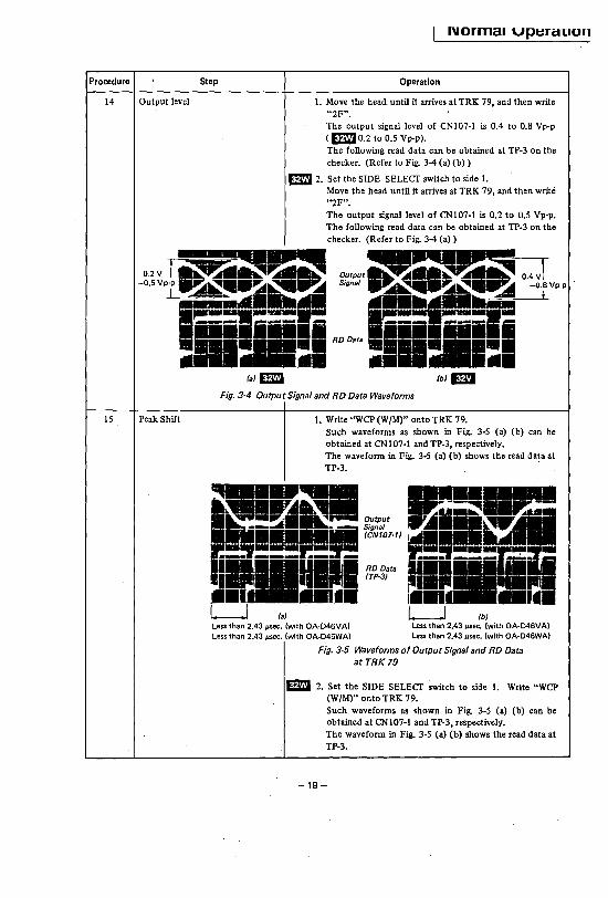
I~ormal uperculull
Procedure Step Operation
14 Output level
15 Peak Shift
(a)e
1. Move the head. until it arrives at TRK 79, and then write "2F". The output signal level of CNI07-1 is 0.4 to 0.8 Vp-p ( Em 0.2 to 0.5 Vp-p). The following read data can be obtained at TP-3 on the checker. (Refer to Fig. 3-4 (a) (b) )
£Em 2. Set the SIDE SELECT switch to side 1. Move the head until it arrives at TRK 79, and then write "2F". The output signal level of CNI07-1 is 0.2 to 0.5 Vp-p. The following read data can be obtained at TP-3 on the checker. (Refer to Fig. 3-4 (a) )
Output Signal
RD Data
(b)EED
Fig. 3-4 Output Signal and RD Data Waveforms
1. Write "WCP (W 1M)" onto TRK 79. Such waveforms as shown in Fig. 3-5 (a) (b) can be obtained at CNI07-1 and TP-3, respectively. The waveform in Fig. 3-5 (a) (b) shows the read da~a at TP-3.
Output Signal (eNt07-t)
RD Data (TP-3)
(b) Less than 2.43 jlsec. (with OA-D46VA) Less than 2.43 jlSec. (with OA-D46VA) Less than 2.43 jlSec. (with OA-D46WAI Less than 2.43 jlSec. (with OA-D46WAI
Fig. 3-5 Waveforms of Output Signal and RD Data at TRK 79
Em!I 2. Set the SIDE SELECT switch to side 1. Write "wep (W/M)" onto TRK 79. Such waveforms as shown in Fig. 3-5 (a) (b) can be obtained at CNI07-1 and TP-3, respectively. The waveform in Fig. 3-5 (a) (b) shows the read data at TP-3.
-19-
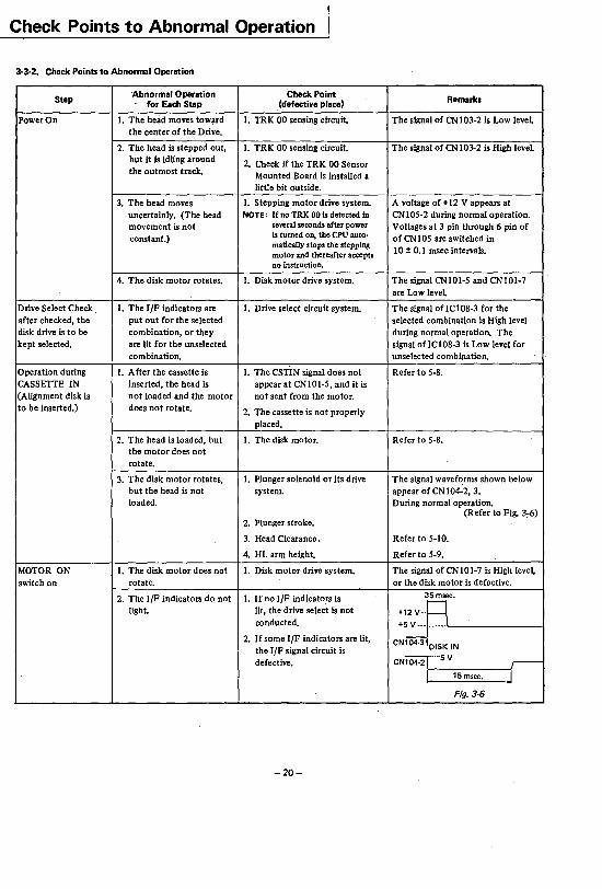
Check Points to Abnormal Operation
3-3-2. Check Points to Abnormal Operation
Step
Power On
Drive Select Check after checked, the disk drive is to be kept selected.
Operation during CASSETTE IN (Alignment disk is to be inserted.)
'Abnormal Operation for Each Step
I. The head moves tow!U'd the center of the Drive,
2. The head is stepped out, but it is idling around the outmost track.
3. The head moves uncertainly. (The head movement is not constant.)
4. The disk motor rotates.
1. The IfF indicators are put out for the selected combination, or they are lit for the unselected combination.
1. After the cassette is inserted, the head is not loaded and the motor does not rotate.
2. The head is loaded, but the motor does not rotate.
3. The disk motor rotates, but the head is not loaded.
Check Point (defective place)
1. TRK 00 sensing circuit.
1. TRK 00 sensing circuit.
2. Check if the TRK 00 Sensor Mounted Board is installed a little bit outside.
1. Stepping motor drive system. NOTE: If no TRK 00 is detected in
several seconds after power is turned on, the CPU automatically stops the stepping motor and thereafter accepts no instruction.
1. Disk motor drive system.
1. Drive select circuit system.
I. The CSTiN signal does not appear at CNIOI-5, and it is not sent from the motor.
2. The cassette is not properly placed.
1. The disk motor.
1. Plunger solenoid or its drive system.
2. Plunger stroke.
3. Head Clearance.
4. HL arm height.
MOTOR ON switch on
1. The disk motor does not 1. Disk motor drive system. rotate.
2. The IJF indicators do not light.
1. If no IfF indicators is lit, the drive select is not conducted.
2. If some IfF indicators are lit, the IfF signal circuit is defective.
-20-
Remarks
The signal of CN 103-2 is Low level
The signal of CN 103-2 is High level
A voltage of +12 V appears at CNI05-2 during normal operation. Voltages at 3 pin through 6 pin of of CN I 05 are switched in 10 ± 0.1 msec intervals.
The signal CNIOI-5 and CNIOI-7 are Low level
The signal ofICIOB-3 for the selected combination is High level during normal operation. The signal ofICIOB-3 is Low level for unselected combipation.
Refer to 5-B.
Refer to 5-B.
The signal waveforms shown below appear of CNI04-2, 3. During normal operation.
Refer to 5-10.
Refer to 5-9.
(Refer to Fig. 3~6)
The signal of CN 101-7 is High level, or the disk motor is defective.
:~-'---------------I CN104.3'OISK IN
CN104·2 """5 V r--l--l-15-m-sec-. --(I
Fig. 3-6
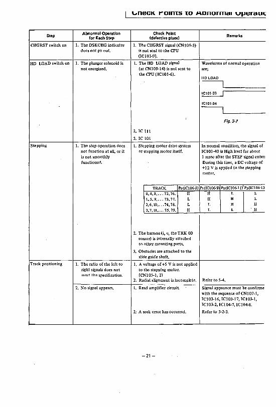
Step
CHGRST switch on
Abnormal Operation for Each Step
1. The DSKCHG indicator does not go out.
HD LOAD switch on I. The plunger solenoid is
Stepping
Track positioning
not energized.
1. The step operation does not function at all, or it is not smoothly functioned.
1. The ratio of the left to right signals does not meet the specification.
2. No signal appears.
\,neCK 1""01n(5 "(0 ADnormi:1I Uptni:nU;
Check Point (defective place)
1. The CHGRST signal (CN I 09-3) is not sent to the CPU (ICIOI-9).
1. The HD WAD signal (at CNI09-14) is not sent to the CPU (ICIOI-6).
2. IC 111
3. IC 101
1. Stepping motor drive system or stepping motor itself.
TRACK, Po(lC106·5) 0,4,8, ••• 72,76. H
1,5,9, ••• 73,77. L
2,6,10, .•• 74,78. L
3,7,11, •.. 75,79. H
2. The harness (i, e, the TRK 00 sensor) is internally attached to other mounting parts.
3. Obstacles are attached to the slide guide shaft.
1. A voltage of +5 V is not applied to the stepping motor. (CNIOS-l,2)
Remarks
Waveforms of normal operation are;
HD LOAD
IC101-33 I
IC101·34
Fig. 3-7
In normal condition, the signal of ICIOI-40 is High level for about 1 msec after the STEP signal enten During this time, a DC voltage of +12 V is applied to the stepping motor.
PI (lCI06-9) Pl(lCI06-11) P3(lCI06-13 H L L
H H L
L H H
L L H
2. Radial alignment is incomplete. Refer to 5-4.
1. Read amplifier circuit.
2; A seek error has occurred.
-21-
Signal appeance must be confirme with the sequence ofCN107-1, ICI03-16, ICI03-17, ICI03-1, ICI03-2, ICI04-7, ICI04-8.
Refer to 3-2-3.
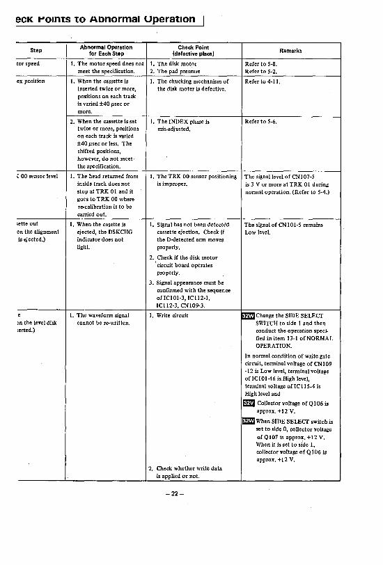
eCK 1"0lnt8 to ADnOrmal uperatlon
Step Abnormal Operation Check Point Remarks for Each Step (defective place)
tor speed I. The motor speed does not 1. The disk motor Refer to 5-S. meet the specification. 2. The pad pressure Refer to 5-2.
ex position 1. When the cassette is 1. The chucking mechanism of Refer to 4-11. inserted twice or more, the disk moter is defective. positions on each track is varied ±40 p.sec or more.
2. When the cassette is set 1. The INDEX phase is Refer to 5-6. twice or more, positions mis-adjusted. on each track is varied ±40 p.sec or less. The shifted positions, however, do not meet· the specification.
C 00 sensor level I. The head returned from 1. The TRK 00 sensor positioning The signal level of CNI07-5 inside track does not is improper. is 3 V or more at TRK 01 during stop at TRK 0 I and it normal operation. (Refer to 5-4.) goes to TRK 00 where re-calibration is to be carried out.
;ette out 1. When the casette is 1. Signal has not been detecte'd The signal of CNIOI-5 remains en the alignment ejected, the DSKCHG cassette ejection. Check if Low level. is ej ected.) indicator does not the D-detected arm moves
light. properly.
2. Check if the disk motor I circuit board operates properly.
3. Signal appearance must be confirmed with the sequence oflCI01-3,ICI12-I, IC112-3, CNI09-3.
e I. The waveform signal I. Write circuit /EEChange the SIDE SELECT m the level disk cannot be re-written. SWITCH to side I and then ;erted.) conduct the operation speci-
fied in item 13-1 of NORMAL OPERATION.
In normal condition of write gate circuit, terminal voltage of CNI09 -12 is Low level, terminal voltage of ICI01-46 is High level, terminal voltage oflC 11 5-4 is High level and
Em Collector voltage of Q 106 is approx. +12·V.
ED When SIDE SELECT switch is set to side 0, collector voltage ofQI07 is approx. +12 V. When it is set to side I, collector voltage of Q 106 is approx.+12 V.
2. Check whether write data is applied or not.
-22-
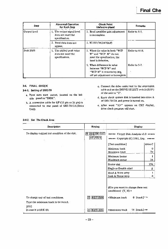
Step
Output level
Peak Shift
3-4. FINAL CHECK
3-4-1. Setting of SMC·70
Abnormal Operation for Each Step
1. The output signallevel does not meet the specification.
2. Read data does not appear.
1. The shifted peak value does not meet the specification.
a. Place auto start switch located on the left side panel to "DISK".
b. A conversion cable for IfF (25 pin to 26 pin) is connected to rear panel of SMI-7012A(Drive Unit).
3-4-2. Set The Check Area
Description
To display original test condition of the disk.
To change any of test conditions.
Type the minimum track to be tested.
[EX] In case it is TRK 00.
Final Che
Check Point Remarks (defective place)
1. Read amplifier gain adjustment Refer to 5-7. is incomplete.
1. ICI03 (MC3470AP)
1. When the value in both "WCP Refer to 4-14. W" and "WCP M" do not meet the specification, the head is defective.
2. When difference in value Refer to 5-7. between "WCP W" and "WCP M" is remarkably Big, off set adjustment is incomplete.
c. Connect the drive under test to the conversion cable and set the DRIVE SELECT switch(SIOI) of the unit to "2".
d. Error check system disk is inserted into drive A of SMI-70 12A and power is turned on.
e. After word "A>" appears on CRT display, drive check program will start.
Keying Display
~ llil rnHWJ ITl ra I RETURN I
• .... Floppy Disk Analysis v3.0 .....
..... Copyright (C) 1981. Sep. .. ...
[Test condition] drive C
Minimum track Maximum track
Minimum Sector Maximum sector
Sector size
Single or Double side?
Read & Write retry Seek & Horne retry
#Do you want to change these test conditions? (Y, N) =
0 79
I 16
256
S
I 0
[X] IRETURNI +Minimum track o [track]=~
@] I RETURN I +Maximum track 79 [track]=~
-23-
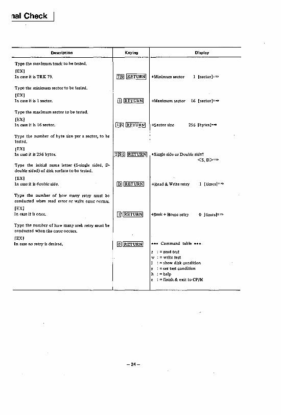
nal Check
Description
Type the maximum track to be tested.
[EX] In case it is TRK 79.
Type the minimum sector to be tested.
[EX] In case it is I sector.
Type the maximum sector to be tested.
[EX] In case it is 16 sector.
Type the number of byte size per a sector, to be tested.
[EX] In case it is 256 bytes.
Type the initial name letter (S-single sided, Ddouble sided) of disk surface to be tested.
[EX] In case it is double side.
Type the number of how many retry must be conducted when read error or write error occurs.
[EX] In case it is once.
Type the number of how many seek retry must be conducted when the error occurs.
[EX) In case no retry is desired.
Keying Display
ID2IIRETURNI +Minimum sector I [sector)=~
m IRETURNI +Maximum sector 16 [sector)=~
rn~ IRETURNI +Sector size 256 [bytes)=~
~[§] IRETURNI +Single side or Double side? <S,D>:~
[Q] IRETURNI +Read & Write retry I [times)=~
-24-
+Seek + Home retry o [times)=~
...... Command table ......
r : = read test w : = write test
: = show disk condition s : = set test condition h : = help e : = finish & exit to CP 1M
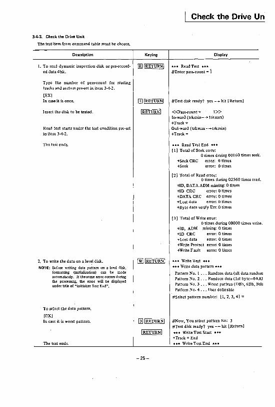
3-4-3. Check the Drive Unit
The test item from command table must be chosen.
Description Keying
1. To read dynamic inspection disk or pre-record- [B] !RETURN! ed data disk.
Type the number of pass-count for reading tracks and sectors pre~et in item 3-4-2.
[EX) In case it is once.
Insert the disk to be tested.
Read test starts under the test condition pre-set in item 3-4-2.
The test ends.
Check the Drive Un
*** Read Test *** #Enter pass-count = i
Display
#Test disk ready? yes - .. hit [Return)
<<Pass-count = I» In-ward (trkmin- -+ trkmax) +Track = Out-ward (trkmax--+trkrnin) +Track =
u* Read Test End [I) Total of Seek error:
o times during 00160 times seek. +Seek eRC error: 0 times +Seek error: 0 times
[2) Total of Read error: o times during 02560 times read.
+10, DATA ADM missing: 0 times +ID eRC error: 0 times +DATA eRe error: 0 times +Lost data error: 0 times +Byte data verify Err: 0 times
[3) Total of Write error: o times during 00000 times write.
+ID, ADM missing: 0 times +10 eRe error: 0 times +Lost data error: 0 times +Write Protect error: 0 times +Write Fault error: 0 times
2. To write the data on a level disk. ~ !RETURNI *u Write Test ***
NOTE: Before writing data pattern on a level disk, formatting (initialization) can be mode automaticaly. If the some error occurs during the processing, the error will be displayed under title of "Initialize Test End".
To select the data pattern.
[EX) In case it is worst pattern.
The test ends.
*** Write data pattern *** Pattern No. I ... Random data (all data random Pattern No.2 ... Random data (1st byte-OAM Pattern No.3 ... Worst pattern (DBh, 6Dh, B611 Pattern No.4 ... User definable
#Select pattern number: [1,2, 3,4) =
[] \RETURN! #Now, You select pattern No: 3
\ RETURN \
-25-
#Test disk ready? yes - - hit [Return)
*** Write Test Start *** +Track = End *** Write Test End ***
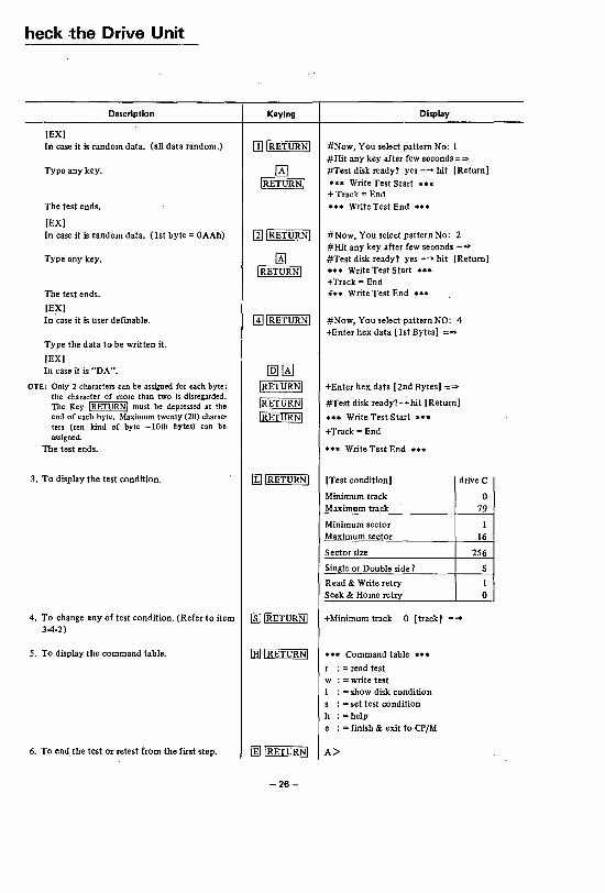
heck the Drive Unit
Description
[EX) In case it is random data. (all data random.)
Type any key.
The test ends.
[EX) In case it is random data. (1st byte = OAAh)
Type any key.
The test ends.
[EX) In case it is user definable.
Type the data to be written it.
[EX) In case it is "DA".
OTE: Only 2 characters can be assigned for each byte; the character of more than two is disregarded. The Key IRETURNI must be depressed at the end of each byte. Maximum twenty (20) characters (ten kind of byte -10th bytes) can be assigned.
The test ends.
3. To display the test condition.
Keying
ITJI RETURN I
[Xl IRETURNI
[i] I RETURN I
IAl IRETURNI
Display
#Now, You select pattern No: 1 #Hit any key after few seconds = => #Test disk ready? yes -~ hit [Return) ••• Write Test Start ... + Track = End ••• Write Test End ...
#Now, You select pattern No: 2 #Hit any key after few seconds ==> #Test disk ready? yes -~ hit [Return) ••• Write Test Start ••• +Track = End ••• Write Test End •••
@]IRETURNI #Now, You select pattern NO: 4 +Enter hex data [1st Bytes) ==>
[QJOO IRETURNI
/RETURNI
IRETURNI
+Enter hex data [2nd Bytes) ==>
#Test disk ready?--hit [Return)
••• Write Test Start •••
+Track = End
• •• Write Test End •••
[Test condition) drive C
Minimum track 0 Maximum track 79
Minimum sector 1 Maximum sector 16
Sector size 256
Single or Double side 1 S
Read & Write retry 1 Seek & Home retry 0
4. To change any of test condition. (Refer to item lID IRETURNI +Minimum track 0 [track) = => 3-4-2}
5. To display the command table.
6. To end. the test or retest from the first step.
(HJ / RETURNI ... Command table
r : = read test w : = write test
: = show disk condition s : = set test condition h : = help e : = finish & exit to CP/M
lliJ I RETURN I A>
-26-
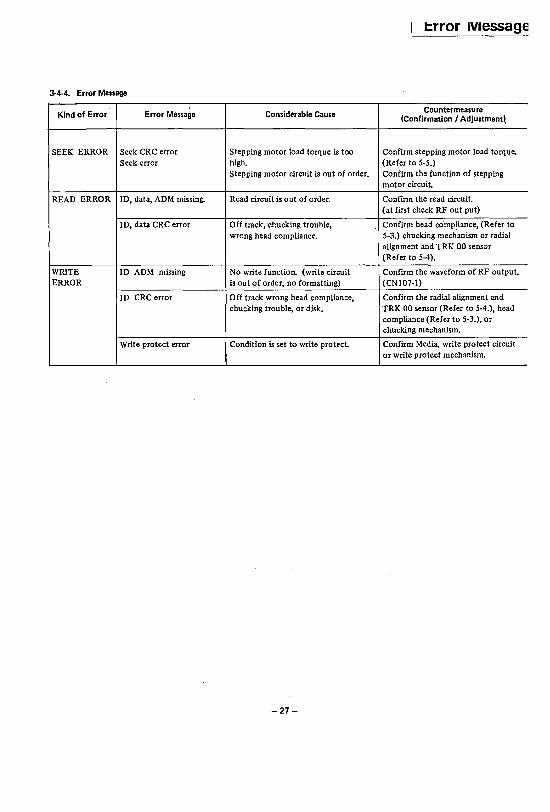
I:rror IVlessage
3-4-4. Error Message
I Countermeasure
I
Kind of Error Error Message Considerable Cause (Confirmation I Adjustmentl.
SEEK ERROR Seek CRC error Stepping motor load torque is too Confirm stepping motor load torque. Seek error high. (Refer to 5-5.)
Stepping motor circuit is out of order. Confirm the function of stepping motor circuit.
READ ERROR 10, data, ADM missing. Read circuit is out of order. Confirm the read circuit. (at first check RF out put)
ID, data CRC error Off track, ·chucking trouble, Confirm head compliance, (Refer to wrong head compliance. 5-3.) chucking mechanism or radial
alignment and TRK 00 sensor (Refer to 5-4).
WRITE 10 ADM missing No write function. (write circuit Confirm the waveform of RF output. ERROR is out of order, no formatting) (CNI07-1)
ID CRC error Off track wrong head compliance, Confirm the radial alignment and chucking trouble, or disk. TRK 00 sensor (Refer to 5-4.), head
compliance (Refer to 5-3.), or chucking mechanism.
Write protect error Condition is set to write protect. Confirm Media, write protect circuit or write protect mechanism.
-27-

MEMO
...............................................................................................................................................................................................................
-28-
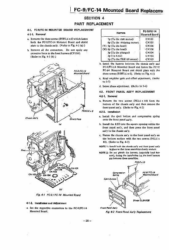
FC-9/FC-14 Mounted Board Replacem.
SECTION 4
PART REPLACEMENT
4·1. FC·9/FC·14 MOUNTED BOARD REPLACEMENT
4-1·1. Removal
a. Remove the three screws (PSW2.6 x 6) which fasten both the FC·9/FC·14 Mounted Board and shield plate to the chassis ass'y. (Refer to Fig. 4·1 (a»
b. Remove all the connectors. Do not apply any excessive force to the head harness (CNI06). (Refer to Fig. 4·1 (b) )
(a)
Boss-"t-+_--"'~
(b)
Fig.4-1 FC·9/FC·14 Mounted Board
4-1-2. Installation and Adjustment
a. Set the respective connectors to the FC·9/FC-14 Mounted Board.
-29-
Harness FC·9/FC·14
Mounted Boord
7p (To the disk motor) CNIOI 6p (To the stepping motor) CNI05
(V) 5p (To the head) CNI06 (W) 6p (To the head) . CNI06
3p (To the plunger) CNI04 3p (To LED) CN102 3p (To the TRK 00 sensor) CNI03
b. Insert the harness between the chassis ass'y and FC·9/FC-14 Mounted Board and fasten the FC-9/ FC-14 Mounted Board and shield plate with the three screws (PSW2.6 x 6). (Refer to Fig. 4-1)
c. Read amplifier gain and offset adjustment. (Refer to 5-7)
d. Index phase adjustment. (Refer to 5-6)
4·2. FRONT PANEL ASS'Y REPLACEMENT
4·2·1. Removal
a. Remove the two screws (PS2.6 x 10) from the bottom of the chassis ass'y and then remove the front panel ass'y. (Refer to Fig. 4-2)
4-2·2. Installation
a. Install the eject button and compression spring onto the front panel ass'y.
b. Install the LED into the square opening within the front panel ass'y, and then press the front panel ass'y to the chassis ass'y. .
c. Fasten the chassis ass'y to the front panel ass'y on the bottom surface with the two screws (PS2.6 x 10). (Refer to Fig. 4-2)
NOTE 1: Install both the chassis ass'y and front panel ass'y in place so that these assemblies closely contact.
NOTE 2: Do not pintch the harness, (especially head har· ness), during the installation i.e, the head harness gap between these assemblies.
PS26x10
eom",.,.M r7~:( FC.S/FC'14 Spring ~~ I:? Mounted Board
E .. 'S.",.,\ ~ i ~ ~~~~II
~ ~ ~ O_GL9PR2fJ
Front pa!,ASS'Y
Fig. 4-2 Front Panel Ass'y Replacement
lind Panel Replacement
-3. BLIND PANEL REPLACEMENT
-3·1. Removal
Remove the front panel ass'y. (Refer to 4·2)
Remove the blind panel by twisting it into the arrow while pressing its both edges. (Refer to Fig. 4·3)
-3·2. Installation
Press the blind panel toward the cassette·up ass'y and latch the two tabs onto the disk holder. (Refer to Fig. 4·3)
Install the front panel ass'y. (Refer-to 4·2)
Disk Holder
Fig. 4·3 Blind Panel Replacement
II. LED MOUNTED BOARD ASS'Y REPLACEMENT
11·1. Removal
Remove both the FC·9/FC·14 Mounted Board and shield plate. Disconnect CN 102 connector. (Refer to Fig. 44 (a) )
Remove the front panel ass'y. (Refer to 4·2)
Remove the LED Mounted Board ass'y from the chassis ass'y.
44·2. Installation
a. Peel off remover from the cushion and set the LED Mounted Board as shown in Fig. 4-4 (b).
b. Install both the FC·9/FC·14 Mounted Board and shield plate. (Refer to 4·1)
c. Install the front panel ass'y. (Refer to 4·2)
PS2.6x 10
LED Mounted Board Ass'y
(al
RED
BLK (bl
Fig. 4-4 LED Mounted Board Ass'y Replacement
-30-
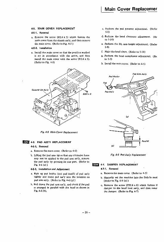
4-5. MAIN COVER REPLACEMENT
4-5·1. Removal
a. Remove the screw (B2.6 x 5) which fastens the main cover from the chassis ass'y, and then remove the main cover. (Refer to Fig. 4-5 )
4-5·2. Installation
a. Install the main cover so that the position marked is set in accordance with the arrow, and then install the main cover with the screw (B2.6 x 5). (Refer to Fig. 4-5)
Fig. 4·5 Main Cover Replacement
1m 4-6. PAD ASS'Y REPLACEMENT
4~-1. Removal
a. Remove the main cover. (Refer to 4-5)
b. Lifting the'pad arm tip so that any excessive force may not be applied to the pad arm ass'y. remove the pad ass'y by pressing its rear part. (Refer to Fig. 4~ (a»
4~-2. Installation and Adjustment
a. Pick up pad holder (not pad itself) of pad ass'y lightly and insert pad ass'y into the location on pad arm ass'y. (Refer to Fig. 4~ (a) )
b. Pull down the pad arm ass'y, and check if the pad is arranged in parallel with the head as shown in Fig. 4~ (b).
-31-
Main Cover Replacemer
c. Perform the pad pressure adjustment. (Refer 5-2)
d. Perform the head clearance adjustment. (Re to 5-10)
e. Perform the HL arm height adjustment. (Refer 5-9)
f. Make the head clean. (Refer to 5-11)
g. Perform the head compliance adjustment. (Re: to 5-3)
h. Install the main cover. (Refer to 4-5)
Pad Arm Ass'y Pad Holder
P~-~---= Pad Ass'y
(a)
Fig. 4-6 Pad Ass'y Replacement
EmJ 4-7. DAMPER REPLACEMENT
4-7-1. Removal
a. Remove the main cover. (Refer to 4-5)
b. Manually set the machine into the Disk-In mod (Refer to Fig. 4-9 (a) )
c. Remove the screw (PS2.6 x 6) which fastens t1 damper to the head load ass'y, and then remo' the damper. (Refer to Fig. 4-7)
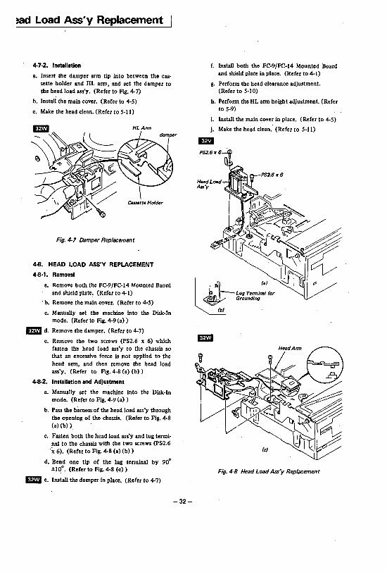
!ad Load Ass'y Replacement
4·7·2. Installation
a. Insert the damper arm tip into between the cassette holder and HL arm, and set the damper to the head load ass'y. (Refer to Fig. 4·7)
b. Install the main cover. (Refer to 4·5)
c. Make. the head clean. (Refer to 5·11)
Fig. 4·7 Damper Replacement
4-8. HEAD LOAD ASS'V REPLACEMENT
4-8·1. Removal
a. Remove both the FC·9/FC·14 Mounted Baord and shield plate: (Refer to 4-1)
. b. Remove the main cover. (Refer to 4·5)
c. Manually set the machine into the Disk· In mode. (Refer to Fig. 4·9 (a) )
Em d. Remove the damper. (Refer to 4·7)
e. Remove the two screws (PS2.6 x 6) which fasten the head load ass'y to the chassis so that an excessive force is not applied to the head arm, and then remove the head load ass'y, (Refer to Fig. 4·8 (a) (b) )
4-8·2. Installation and Adjustment
a. Manually set the machine into the Disk·In mode. (Refer to Fig. 4·9 (a) )
b. Pass the harness of the head load ass'y through the opening of the chassis. (Refer to Fig. 4-8 (a) (b) )
c. Fasten both the head load ass'y and lug terminal to the chassis with the two screws (PS2.6 it 6). (Refer to Fig. 4-8 (a) (b) )
d. Bend one tip of the lug terminal by 900
±I~o. (Refer to Fig. 4-8 (c»
Em e. Install the damper in place. (Refer to 4-7)
-32-
f. Install both the FC·9/FC·14 Mounted Board and shield plate in place. (Refer to 4-1)
g. Perform the head clearance adjustment. (Refer to 5·10)
h. Perform the HL arm height adjustment. (Refer to 5·9)
i. Install the main cover in place. (Refer to 4-5)
j. Make the head clean. (Refer to 5·11)
Fig. 4-8 Head Load Ass'y Replacement
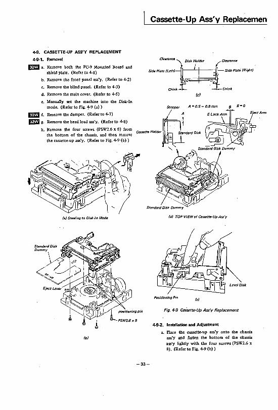
4-9. CASSETTE-UP ASS'V REPLACEMENT
4-9-1. Removal
_ a. Remove both the FC-9 Mounted Board and shield plate. (Refer to 4-1)
b. Remove the front panel ass'y. (Refer to 4-2)
c. Remove the blind panel. (Refer to 4-3)
d. Remove the main cover. (Refer to 4-5)
e. Manually set the machine into the Disk-In mode. (Refer to Fig. 4-9 (a) )
_ f. Remove the damper. (Refer to 4-7)
_ So Remove the head load ass'y. (Refer to 4-8)
h. Remove the four screws (PSW2.6 x 8) from the bottom of the chassis, and then remove the cassette-up ass'y. (Refer to Fig. 4-9 (b) )
(a) Steeling to Disk-In Mode
(b)
Cassette-Up Ass'y Replacemen
Clearancs Clearancs
Side Plata (Left)_JIIJ---L.-+----i, Side Plata (Right)
OJink-l -1LChink
(c)
Stopper A-0.5-o.8mm 8 8-0
~~H.fd" ~ f"~roD;"
-33-
(d) TDP VIEW of Cassetta-Up Ass'y
Positioning Pin (e)
Fig. 4·9 Cassette-Up Ass'y Replacement
4-9-2. Installation and Adjustment
a. Place the cassette-up ass'y onto the chassis ass'y and fasten the bottom of the chassis ass'ylightly with the four screws (PSW2.6 x 8). (Refer to Fig. 4-9 (b»
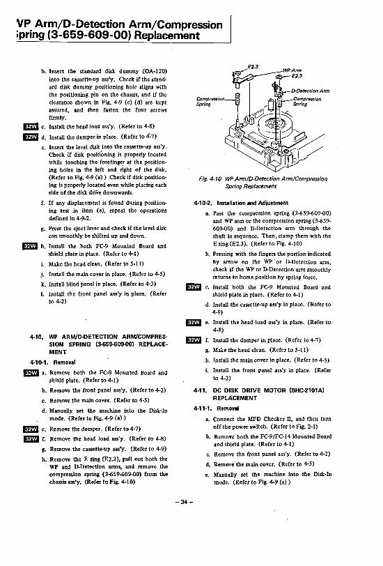
'VP Arm/D-Detection Arm/Compression ~pring (3-659-609-00) Replacement
b. Insert the standard disk dummy (OA-120) into the cassette-up ass'y. Check if the standard disk dummy positioning hole aligns with the positioning pin on the chassis, and if the Clearance shown in Fig. 4-9 (c) (d) are kept assured, and then fasten the four screws firmly.
!Em c. Install the head load ass'y. (Refer to 4-8)
!Em d. Install the damper in place. (Refer to 4-7)
e. Insert the level disk into the cassette-up ·ass'y. Check if disk positioning is properly located while touching the forefinge.r at the positioning holes in the left and right of the disk. (Refer to Fig. 4-9 (e» Check if disk positioning is properly located even while placing each side of the disk drive downwards.
f. If any displacement is found during positioning test in item (e), repeat the operations defined in 4-9-2.
g. Press the eject lever and check if the level disk can smoothly be shifted up and down.
!Em h. Install the both FC-9 Mounted Board and shield plate in place. (Refer to 4-1)
i. Make the head Clean. (Refer to 5-11)
j. Install the main cover in place. (Refer to 4-5)
k. Install blind panel in place. (Refer to 4-3)
1. Install the front panel ass'y in place. (Refer to 4-2)
4-10. WP ARM/D-DETECTION ARM/COMPRESSION SPRING (3-659-609-00) REPLACEMENT
4-10-1. Removal
!Em a. Remove both the FC-9 Mounted Board and shield plate. (Refer to 4-1)
h. Remove the front panel ass'y. (Refer to 4-2)
c. Remove the main cover. (Refer to 4-5)
d. Manually set the machine into the Disk-In mode. (Refer to Fig. 4-9 (a) )
Em e. Remove the damper. (Refer to 4-7)
!Em f. Remove thjl head load ass'y. (Refer to 4-8)
g. Remove the cassette-up ass'y. (Refer to 4-9)
h. Remove the E ring (E2.3), pull out both the WP and D-Detection arms, and remove the compression spring (3-659-609-00) from the chassis ass'y. (Refer to Fig. 4-10)
~E2.3 WPArm
~E2.3 D-Detection Arm
Fig. 4·10 WP Arm/O·Oetection Arm/Compression Spring Replacement
4-10-2. Installation and Adjustment
a. Pass the compression spring (3-659-609-00) and WP arm or the compression spring (3-659-609-00) and D-Detection arm through the shaft in sequence. Then, Clamp them with the E ring (E2.3). (Refer to Fig. 4-10)
b. Pressing with the fingers the portion indicated by arrow on the wp. or D-Detection arm, check if the WP or D-Detection arm smoothly returns to home position by spring force.
!Em c. Install both the FC-9 Mounted Board and shield plate in place. (Refer to 4-1)
d. Install the cassette-up ass'y in place. (Refer to 4-9)
!Em e. Install the head load ass'y in place. (Refer to 4~8)
!Em f. Install the damper in place. (Refer to 4-7)
-34-
g. Make the head Clean. (Refer to 5-11)
h. Install the main cover in place. (Refer to 4-5)
i. Install the front panel ass'y in place. (Refer to 4-2)
4-11. DC DISK DRIVE MOTOR (BHC-2101A) REPLACEMENT
4-11-1. Removal
a. Connect the MFD Checker n, and then turn off the power switch. (Refer to Fig. 2-1)
b. Remove both the FC-9/FC-14 Mounted Board and shield plate. (Refer to 4-1)
c. Remove the front panel ass'y. (Refer to 4-2)
d. Remove the main cover. (Refer to 4-5)
e. Manually set the machine into the Disk-In mode. (Refer to Fig. 4-9 (a) )
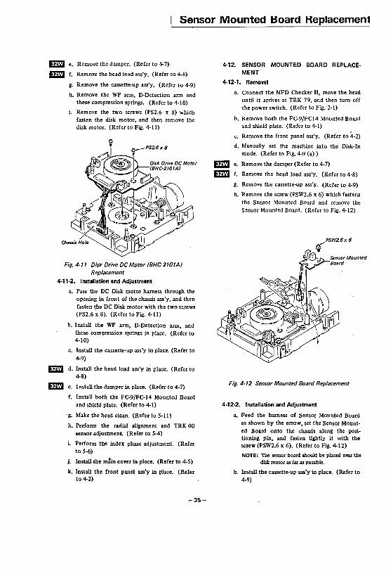
Sensor Mounted Board Replacemen1
Em e. Remove the damper. (Refer to 4-7)
Em f. Remove the head load ass'y. (Refer to 4-8)
g. Remove the cassette-up ass'y. (Refer to 4-9)
h. Remove the WP arm, D-Detection arm and these compression springs. (Refer to 4-10)
i. Remove the two screws (PS2.6 x 8) which fasten the disk motor, and then remove the disk motor. (Refer to Fig. 4-11)
Fig. 4-11 Disk Drive DC Motor (BHC·2101A) Replacement
4-11-2. Installation and Adjustment
a. Pass the DC Disk motor harness through the opening in front of the chassis ass'y, and then fasten the DC Disk motor with the two screws (PS2.6 ~ '8). (Refer to Fig. 4-11)
b. Install the WP arm, D-Detection arm, and these compression springS in place. (Refer to 4-10)
c. Install the cassette-up ass'y in place. (Refer to 4-9)
Em d. Install the head load ass'y in place. (Refer to 4-8)
EmJ e. Install the damper in place. (Refer to 4-7)
f. Install both the FC-9/FC-14 Mounted Board and shield plate. (Refer to 4-1)
'g. Make the head clean. (Refer to 5-11)
h. Perform the radial alignment and TRK 00 sensor adjustment. (Refer to 5-4)
L Perform the index phase adjustment. (Refer to 5-6)
j. Install the m:in cover in place. (Refer to 4-5)
k. Install the front panel ass'y in place. (Refer to 4-2)
-35-
4-12. SENSOR MOUNTED BOARD REPLACE· MENT
4·12·1. Removal
a. Connect the MFD Checker II, move the head until it arrives at TRK 79, and then turn off the power switch. (Refer to Fig. 2·1)
b. Remove both the FC·9/FC14 Mounted Board and shield plate. (Refer to 4-1)
c. Remove the front panel ass'y. (Refer to 4-2)
d. Manually set the machine into the Disk·In mode. (Refer to Fig. 4·9 (a) )
Em e. Remove the damper (Refer to 4-7)
Em f. Remove the head load ass'y. (Refer to 4-8)
g. Remove the cassette-up ass'y. (Refer to 4-9)
h. Remove the screw (PSW2.6 x 6) which fastens the Sensor Mounted Board and remove the Sensor Mounted Board. (Refer to Fig. 4-12)
Fig. 4·12 Sensor Mounted Board Replacement
4·12·2. Installation and Adjustment
a. Feed the harness of Sensor Mounted Board as shown by the arrow, set the Sensor Mounted Board onto the chassis along the positioning pin, and fasten lightly it with the screw (PSW2.6 x 6). (Refer to Fig. 4-12)
NOTE: The sensor board should be placed near the disk motor as far as possible.
b. Install the cassette-up ass'y in place. (Refer to 4-9)
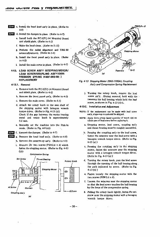
_ c. Install the head load ass'y in place. (Refer to 4-8)
_ d. Install the damper in place. (Refer to 4-7)
e. Install both the FC-9/FC-14 Mounted Board and shield plate. (Refer to 4-0·
f. Make the head clean. (Refer to 5-11)
g. Perform the radial alignment and TRK 00 sensor adjustment. (Refer to 5-4)
h. Install the front panel ass'y in place. (Refer to 4-2)
i. Install the main cover in place. (Refer to 4-5)
4-13. LEAD SCREW ASS'Y (STEPPING MqTOR/ LEAD SCREW/COUPLING ASS'Y/COMPRESSION SPRING (4-601-083-00) ) REPLACEMENT
4-13.1. Removal
a. Remove both the FC-9/FC-14 Mounted Board and shield plate. (Refer to 4-0
b. Remove the front panel ass'y. (Refer to 4-2)
c. Remove the main cover. (Refer to 4-5)
d. Attach the rotary knob to the rear shaft of the stepping motor with hexagon wrench torque driver. (Refer to Fig. 4-13 (a» Check if the gap between the motor bearing metal and rotary knob is approximately 0.5mm.
e. Manually set the machine into the Disk-In mode. (Refer ·to Fig. 4-9 (a»
_ f. Remove the damper. (Refer to 4-7)
_ g. Remove the head load ass'y. (Refer to 4-8)
h. Remove the cassette-up ass'y. (Refer to 4-9)
i. Remove die two screws (PSW2.6 x 6) which fasten the stepping motor. (Refer to Fig. 4-13 (b»
Compression Spring
Rotary Knob
Stepping Motor
jJ Coupling Ass'y
(a)
-36-
Fig. 4·13 Stepping Motor (SNS-1100A). Coupling Ass'y and Compression Spring Replacement·
j. Turning the rotary knob, remove the lead screw ass'y ... During removal, hold with the tweezers the ball bearing which hold the lead screw, as shown in Fig. 4-13 (b)-I.
4-13-2. Installation and Adjustment
NOTE: If the replacement can be made with lead screw ass'y, steps. up to II should be skipped.
NOTE: Apply Sony grease (same quantity of watch tip) on whole area of lead screw before replacing it.
a. Stepping motor, lead screw, coupling ass'y and thrust bearing must be roughly assembled·.
b. Pressing the coupling ass'y to the lead screw, fasten the setscrew near the lead screw with a hexagon wrench torque driver. (Refer to Fig. 4-13 (a) )
c. Pressing the coupling ass'y to th~ stepping motor, fasten the setscrew near the stepping motor with a hexagon wrench torque dirver. (Refer to Fig. 4-13 (a) )
d. Turning the rotary knob, pass the lead screw through the opening of the ball bearing along the path indicated by arrow. (Refer to Fig. 4-13 (b»
e. Fasten loosely the stepping motor with the two screws (PSW2.6 x 6).
f. Loosen the setscrew near the stepping motor so that the lead screw touches the ball bearing by the force of the compression spring.
g. Pulling the rotary knob lightly, fasten the setsCrew near the stepping motor with a hexagon wrench torque driver.
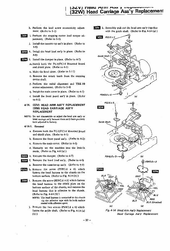
\.:lL V I nt:Clu 1"'\1 III "'~ Y • • ..,t".~'''' ......... ... (32W) Head Carriage Ass'y Replacemen1
h. Perfonn the lead screw eccentricity adjust-ment. (Refer to 5-1) .
D i Perfonn the stepping motor load torque adjustment. (Refer to 5-5)
j. Install the cassette-up ass'y in place. (Refer to 4-9)
Em k. Install the head load ass'y in place. (Refer to 4-8)
Em 1. Install the damper in place. (Refer to 4-7)
m. Install both the FC-9/FCI4 Mounted Board and shield plate. (Refer to 4-1)
n. Make the head clean. (Refer to 5-11)
o. Remove the rotary knob from the stepping motor shaft.
p. Perfonn the radial alignment and TRK 00 sensor adjustment. (Refer to 5-4)
q. Instiill the main cover in place. (Refer to 4-5)
r. Install the front panel ass'y in place. (Refer to 4-2)
4-14. (32V) HEAD ARM ASS'Y REPLACEMENT (32W) HEAD CARRIAGE ASS'Y REPLACEMENT
NOTE: Do not disassemble or adjust the head ann ass'y or head carriage ass'y because these ass'y have precisely been adjusted in factory.
4-14-1. Removal
a. Remove both the FC-9/FCI4 Mounted Board and shield plate. (Refer to 4-1)
b. Remove the front panel ass'y. {Refer to 4-2)1
c. Remove the main cover. (Refer to 4-5)
d. Manually set the machine into the Disk-In mode. (Refer to Fig. 4-9 (a) )
Em e. Remove the damper. (Refer to 4-7)
Em f. Remove the helJ.d load ass'y. (Refer to 4-8)
g. Remove the cassette-up ass'y. (Refer to ~9)
Em h. Remove the screw (PSW2.6 x 6) which fastens the head harness to the chassis on the bottom surface. (Refer to Fig. 4-14 (a»
Em i. Remove the screw (PSW2.6 x 8) which fastens the head harness to the shield plate on the bottom surface of- the chassis, and remove the head harness that is adhesive to the chassis. (Refer to Fig. 4-14 (b) ) NOTE: The head harness is contacted to the chassis
via the adhesive tape with its both surface coated with adhesive agent.
j. Remove the two screws (PSW2.6 x 6) which fasten the guide shaft. {Refer to Fig. 4-14 (a) (b»
-37-
IEEI k. Smoothly pull out the head ann ass'y together with the guide shaft. (Refer to Fig. 4-14 (a) )
PSW2.6 x 9--' (b)
.l""tpSW2.6 x 8
~mm WHT .
(e) (d)
Fig. 4-14 Head Arm Ass'y Replacement Head Carriage Ass'y Replacement
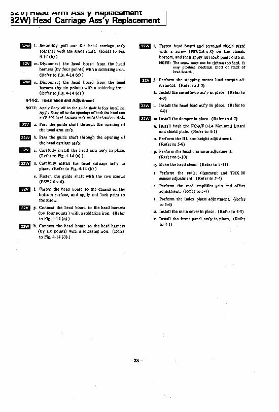
~, v I nt:Clu ",rm "'55 y neplacement 32W) Head Carriage Ass'y Replacement
_ 1. Smoothly pull out the head carriage, ass'y together with the guide shaft. (Refer to Fig. 4-14 (b»
Em m. Disconnect the head board from the head harness (by four points) with a soldering iron. (Refer to Fig. 4-14 (c) )
_ n. Disconnec~ the head board from the head harness (b'y six points) with a soldering iron. (Refer to Fig. 4-14 (d»
4-14-2. Installation and Adjustment
NOTE: Apply Sony oil to the guide shaft before installing. Apply Sony oil to the openings of both the head ann ass'y and head carriage ass'y using the bamboo stick.
a. PaSs the guide shaft through the openmg of the head arm ass'y.
b. Pass the guide shaft through the opening of the head carriage ass'y.
c. Carefully install the head arm ass'y in place. (Refer to Fig. 4-14 (a) )
d. Carefully install the head carriage ass'y in place. (Refer to Fig. 4-14 (b»
e. Fasten the guide shaft with the two screws (PSW2.6 x 6).
Em. f. Fasten the head board to the chassis on the bottom surface, and apply nut lock paint to the screw.
g. Connect the head board to the head harness (by four points) with a soldering iron. (Refer to Fig.' 4-14 (c) )
h. Connect the head board to the head harness (by six points) with a soldering iron. (Refer to Fig. 4-14 (d) )
Em i. Fasten head board and terminal shield plate with a screw (PSW2.6 x 8) on the chassis bottom, and then apply nut lock paint onto it. NOTE: The screw must not be tighten too hard. It
may produce electrical short or' crack of head board.,
Em j. Perform the stepping motor load torque adjustment. (Refer to 5-5)
k. Install the cassette-up ass'y in place. (Refer to 4-9)
IE I. Install the head load ass'y in place. (Refer to 4-8)
_ m.Install the damper in place. (Refer to 4-7)
-38-
n. Install both the FC-9/FC-14 Mounted Board and shield plate. (Refer to 4-1)
o. Perform the HL arm height adjustment. (Refer to 5-9)
p. Perform the head clearance adjustment. (Refer to 5-10)
q'. Make the head clean. (Refer to 5-11)
r. Perform the radial alignment and TRK 00 sensor adjustment. (Refer to 5-4)
s. Perform the read amplifier gain and offset adjustment. (Refer to 5-7)
t. Perform the index phase adjustment. (Refer to 5-6)
u. Install the main cover in place. (Refer to 4-5)
v. ,Install the front panel ass'y in place. (Refer to 4-1)
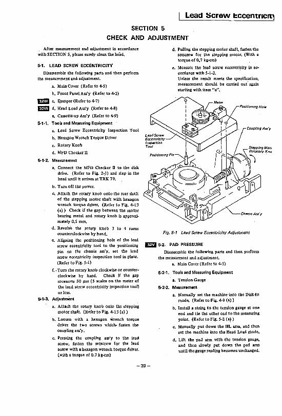
Lead Screw I:ccentrlcn,
SECTION 5 CHECK'AND ADJUSTMENT
After measurement and adjustment in accordance with SECTION 5, please surely clean the head.
5-1. LEAD SCREW ECCENTRICITY
Disassemble the following parts and then perform the measurement and adjustment.
a. Main Cover (Refer to 4-5)
b. Front Panel Ass'y (Refer to 4-2)
ED c. llamper (Refer to 4-7)
ED d. Head Load Ass'y (Refer to 4-8)
e. Cassette-up Ass'y (Refer to 4-9)
5-1-1. Tools and Measuring Equipment
a. Lead Screw Eccentricity Inspection Tool
b. Hexagon Wrench TOIque Driver
c. Rotary Knob
d. MFD Checker 11
5-1·2. Measurement
a. Connect the MFD Checker n to the disk drive. (Refer to Fig, 2-.1) and step in the head until it arrives at TRK 79.
b. Turn off the power.
c. Attach the rotary knob onto the rear shaft of the stepping motor shaft with hexagon wrench tOIque driver. (Refer to Fig. 4-13 (a» Check if the gap between the motor bearing metal and rotary knob is approximately 0.5 mm.
d. Revolve the rotary knob 3 to 4 turns counterclockwise by hand.
e. Aligning the positiOning hole of the lead screw eccentricity tool to the positioning pin on the chassis ass'y, set the lead screw eccentricity inspection tool in place. (Refer to Fig. 5-1)
f. -Turn the rot:uy knob clockwise or counterclockwise by hand. Check if the gap measures SO #lm (5 scales on the meter of the lead screw eccentricity inspection tool) or less.
5-1-3. Adjustment
a. Attach the rotary knob onto the stepping motor shaft. (Refer to Fig. 4-13 (a) )
b. Loosen with a hexagon wrench tOIque driver the two screws which- fasten the coupling ass'y.
c. Pressing the coupling ass'y to the lead screw, fasten the setscrew for the lead screw with a hexagon wrench tOIque driver. (with a tOIque of 0.7 kg-cm)
d. Pulling the stepping motor shaft, fasten the setscrew for the stepping motor. (With a tOIque of 0.7 kg-cm)
e. Measure the lead screw eccentri~ity in accordance with 5-1-2. Unless the result meets the specification, measurement should be carried out' again starting with item "a".
Fig. 5-1 Lead Screw Eccentricity Adjustment
Em 5-2. PAD PRESSURE
Disassemble the following parts and then perform the measurment and adjustment.
a. Main Cover (Refer to 4-5)
5-2-1. Tools and Measuring Equipment
a. Tension Gauge
5-2-2. Measurement
a. Manually set the machine into the Disk-ln mode. (Refer to Fig. 4-9 (a) )
b. Install a string to the tension gauge at one end and tie the other end to the measuring point. (Refer to Fig. 5-2 (a) )
c. Manually put down the HL arm, and then set the machine into the Head Load mode.
d. Lift the pad arm with the tension gauge, and then slowly put down the pad arm until the gauge reading becomes unchanged.
-39-
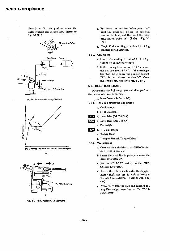
1eaa \,;ompllance
Identify as "A" the position where the stable reading can be obtained. (Refer to Fig. 5-2 (b) )
'-........~ \ M:asuring Point
~ Fan·Shaped Gauge
(a) Pad Pressure Measuring Method
(x) Distance betwfJen surfaces of head and pad.
(b)
(c)
Fig. 5·2 Pad Pressure Adjustment
-40-
e. Put down the pad arm below point "A" until the point just before the pad arm touches the head, and then read the rising peak value at point "B". (Refer to Fig. 5-2 (b»
f. Check if the reading is within II ± 1.5 g specified for adjustment.
5-2·3. Adjustment
a. Unless the reading is out of 11 ± 1.5 g, change the spring set-position.
b. If the reading is in excess of 12.5 g, move the position toward "A". If the reading is less than 9.5 g, move the position toward "B". Do not change position "C" where the string is set. (Refer to Fig. 5-2 (c) )
5-3. HEAD COMPLIANCE
Disassemble the following parts and then perform the measurment and adjustment.
a. Main Cover (Refer to 4-5)
5-3-1. Toolsand Measuring Equipment
a. Oscilloscope
b. MFD Checker II
ED c. Level Disk (OR-D46VA)
m d. Level Disk (OR-D46WA)
e. Pad weight
ED f. e 2 mm Driver
g. Rotary Knob
h. Hexagon Wrench Torque Driver
5-3-2. Measurement
a. Connect the disk drive to the MFD Checker II. (Refer to Fig. 2-1)'
b. Insert the level disk in place, and move the head onto TRK 79.
c. Set the HD LOAD switch on the MFD Checker II to "ON".
d. Attach the rotary knob onto the stepping motor shaft and fIx it with a hexagon wrench torque driver. (Refer to Fig. 4-13 (a»
e. Write "2F" into the disk and check if the amplifier output waveform at CNI07-1 is satisfactory.
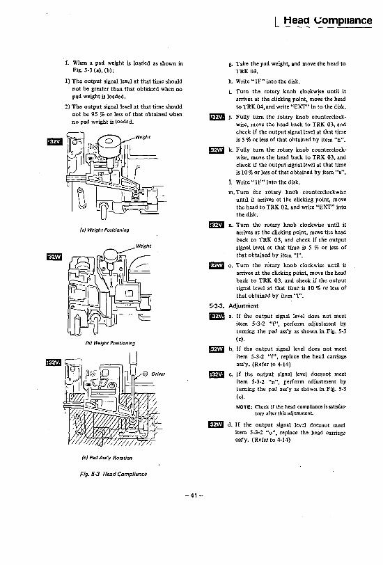
f. When a pad weight is loaded as shown in Fig. 5-3 (a), (b);
1) The output signal level at that time should not be greater than that obtained when no pad weight is loaded.
2) The output signal level at that time should not be 95 % or less of that obtained when no pad weight is loaded.
Heaa l;Ompnance
g. Take the pad weight, and move the head to TRK 03.
h. Write "IF" into the disk.
i. Turn the rotary knob clockwjse until it arrives at the clicking point, move the head to TRK 04, and write "EXT" in to the disk.
m j. Fully turn the rotary knob counterclockwise, move the head back to TRK 03, and check if the output signal level at that time
ED is 5 % or less of that obtained by item "h".
(a) Weight Positioning
(b) Weight Positioning
(c) Pad Ass'y Rotation
Fig. 5-3 Head Complience
-41-
m k. Fully turn the rotary knob counterclockwise, move the head back to TRK 03, and check if the output signal level at that time is 10 % or less of that obtained by item "e".
t. Write "IF" into the disk.
m. Turn the rotary knob counterclockwise until it arrives at the clicking point, move the head to TRK 02, and write "EXT" into the disk.
1m n. Turn the rotary knob clockwise until it arrives at the clicking point, move the head back to TRK 03, and check if the output signal level at that time is 5 % or less of that obtained by item "I" .
• o. Turn the rotary knob clockwise until it arrives at the clicking point, move the head back to TRK 03, and check if the output signal level at that time is 10 % or less of that obtained by item "1".
5-3-3. Adjustment
m a. If the output signal level does not meet item 5-3-2 "f", perform adjustment by turning the pad ass'y as shown in Fig. 5-3 (c).
Em b. If the output signal level does not meet item 5-3-2 "f", replace the head carriage ass'y. (Refer to 4-14)
c. If the output signal level doesnot meet item 5-3-2 "n", perform adjustment by turning the pad ass'y as shown in Fig. 5-3 (c).
NOTE: Check if the head compliance is satisfactal}' after this adjustmenL
Em d. If the output signal level doesnot meet item 5-3-2 "0", replace the head carriage ass'y. (Refer to 4-14)
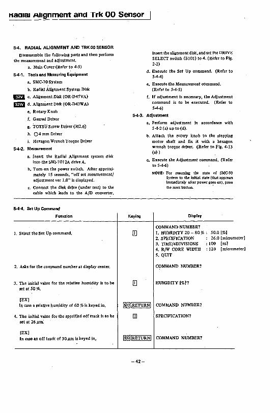
ttaOlal Alignment and Trk 00 Sensor
5-4. RADIAL ALIGNMENT AN> lRKOO SENSOR
Dissassemble the following parts and then perform the measurement and adjustment.
a. Main Cover (Refer to 4-5)
5-4-1. Tools and Measuring Equipment
a. SMC-70 System
b. Radial Alignment System Disk
IESI c. Alignment Disk (OR-D41VA)
EmI d. Alignment Disk (OR-D47WA)
e. Rotary Knob
f. Geared Driver
g. TOTSU Screw Driver (M2.6)
h. 94 mm Driver
i. Hexagon Wrench Torque Driver
5-4-2. Measurement
a. Insert the Radial Alignment system disk into the SMI-7012A drive A.
b. Tum on the power switch. After approximately 15 seconds, "off set measurement/ adjustment vcr 1.0" is displayed.
c. Connect the disk drive (under test) to the cable which leads to the AID converter,
5-4-4. Set Up Command
Function
1. Select the Set Up command.
2. Asks for the corn.mand number at display center.
3. The initial value for the relative humidity is to be set at 50 %.
[EX] In case a relative humidity of 60 % is keyed in,
4. The initial value for the specified off track is to be set at 26 #lm: .
[EX] In case an off track of 30 #lm is keyed in,
insert the alignment disk, and set the DRIVE SELECT switch (SIOl) to 4. (Refer to Fig. 2-2)
d. Execute the Set Up command. (Refer to 5-4-4)
e. Execute the Measurement command. (Refer to 5-4-5)
f. If adjustment is necessary, the Adjustment command is to be executed. (Refer to 5-4-6)
5-4-3. Adjustment
Keying
ill
ill
a. Perform adjustment in accordance with 5-4-2 (a) up to (d).
b. Attach the rotary knob to the stepping motor shaft and fix it with a hexagon wrench torque driver. (Refer to Fig. 4~13 (a»
c. Execute the Adjustment command. (Refer to 5-4-6)
NOTE: For resuming the state of SMC-70 System to the Initial state (that apprears Immediately after power goes on), press the reset button. '
Display
COMMAND NUMBER? 1. HUMIDITY 20 - 80 %: 50.0 [%] 2. SPECIFICATION 3. TIME/4DIVISIONS
26.0 [micrometer] : 100 [ns]
4. R/W CORE WIDTH : 120 [micrometer] 5. QUIT
COMMAND NUMBER?
HUMIDITY [%]?
1§I@lIRETURNI COMMAND NUMBER?
SPECIFICATION?
@I@IRETURN\ COMMAND NUMBER?
-42-
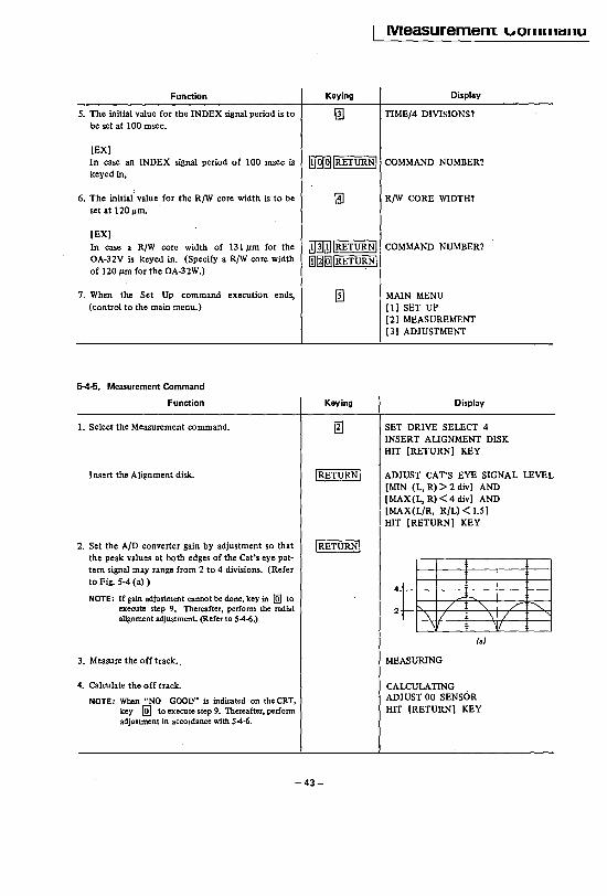
Function
5. The initial value for the INDEX signal period is to be set at 100 msec.
[EX)
Measurement \"omnli:lllU
Keying Display
TIME/4 DIVISIONS?
In case an INDEX signal period of 100 msec is l!l§@]IRETURNI COMMAND NUMBER? keyed in,
6. The initial'value for the R/W core width is to be set at 120 jJIn.
[EX)
In case a R/W core width of l3l/.lm for the OA-32V is keyed in. (Specify a R/W core width of 120 /.lm for the OA-32W.)
7. When the Set Up command execution ends, (control to the main menu.)
5-4-5. Measurement Command
Function
1. Select the Measurement command.
Insert the Alignment disk.
2. Set the AID converter gain by adjustment so that the peak values at both edges of the Cat's eye pattern signal may range from 2 to 4 divisions. (Refer to Fig. 5-4 (a) )
NOTE: If gain adjustment cannot be done, key in [Q] to execute step 9. Thereafter, perform the radial alignment adjustment. (Refer to 54-6.)
3. Measure the off track •.
4. Calculate the off track.
NOTE: When "NO GOOD" is indicated on the CRT, key [Q] to execute step 9. Thereafter, perform adjustment in accordance with 54-6.
R/W CORE WIDTH?
l!l@lillIRETURNI COMMAND NUMBER?
!IJ§IQIIRETU~NI
Keying
MAIN MENU [1) SET UP (2) MEASUREMENT (3) ADJUSTMENT
Display
SET DRIVE SELECT 4 INSERT AUGNMENT DISK HIT [RETURN) KEY
ADJUST CAT'S EYE SIGNAL LEVEL [MIN (L, R) > 2 div) AND [MAX(L, R) < 4 div) AND [MAX(L/R, R/L) < 1.5) fiT [RETURN) KEY
;........ :t / "-\ I
(a)
MEASURING
CALCULATING ADJUST 00 SENSOR HIT [RETURN) KEY
\ I I
L ~
-43-
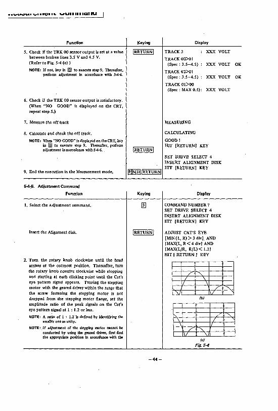
• .,,~ .... '!Wi. I I'!WI I" '"'VI I II Iiallu
Function
5. Check if the TRK 00 sensor output is set at a value between broken lines 3.5 V and 4.5 V. (Refer to Fig. 5-4 (e) )
NOTE: If not, key in lID to execute step 9. Thereafter, perfonn adjustment in accoIdance with S-4~.
6. Check if the TRK 00 sensor output is satisfactory. (When "NO GOOD" is displayed on the CRT, repeat step 5.)
7. Measure the off track
8. Calculate and check the off track.
NOTE: When "NO GOOD" is displayed on the CRT, key in (Q] to execute step 9. Thereafter, perfonn adjustment in accoIdance with S-4~.
9. End the execution in the Measurement mode.
5-4:6. Adjustment Command
Function
1. Select the Adjustment command.
Insert the Alignment disk.
2. Tum the rotary knob clockwise until the head arrives at the outmost position. Thereafter, tum the rotary knob counter clockwise while stopping and starting at each clicking point until the Cat's eye pattern signal appears. Turning the stepping motor with the geared driver within the range that the screw fastening the stepping motor is not dropped from the stepping moter flange, set the amplitude ratio of the peak signals on the Cat's eye pattern signal at 1 : 1.2 or less.
NOTE: A ratio of 1 : 1.2 is defined by identifying the smaller one as unity.
NOTE: If adjustment of the stepping motor cannot be conducted by using the geared driver, fust fmd the appropriate position in accoIdance with the
Keying
I RETURN I
I RETURN I
m@IRETURNI
Keying
I RETURN I
-44-
Display
TRACK 3 XXX VOLT
TRACK 00>01 (Spec: 3.5-4.5) XXX VOLT
TRACK 02>01 (Spec: 3.5-4.5) XXX VOLT
TRACK 01>00 (Spec: MAX 0.5): XXX VOLT
MEASURING
CALCULATING
GOOD! HIT [RETURN) KEY
SET DRIVE SELECT 4 INSERT ALIGNMENT DISK HIT [RETURN) KEY
Display
COMMAND NUMBER? SET DRIVE SELECT 4 INSERT ALIGNMENT DISK HIT [RETURN) KEY
ADJUST CAT'S EYE [MIN(L, R) > 3 divl AND [MAX(L, R<4 div) AND [MAX(L/R, R/L) < 1.2) HIT [ RETURN) KEY
/' "" / \ 11 \
/'
""
I'-. \
\ /'
IV
IV (b)
"" "-"./ (e)
Fig. 54
/ 1/
/"
""
""
OK
OK
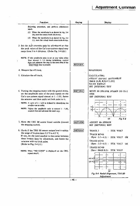
Function
following procedure, and perform adjustment again.
(1) When the waveform is as shown in Fig. 5-4 (b), tum the rotary mob clockwise.
(2) When the waveform is as shown in Fig. 5-4 (c), tum the rotary mob counterclockwise.
J
3. Set the AID converter gain by adjustment so that the peak values of the Cat's eye pattern signal may range from 3 to 4 divisions. (Refer Fig. 5-4 (d) )
NOTE: If the amplitude ratio is set at any value other than utmost 1: 1.2 during initializing, control does not advance the step to the next even if the I RETURN I key is pressed.
4. Measure the off track.
5. Calculate the off track.
6. Turning the stepping motor with the geared driver, set the amplitude ratio of the peak signals on the Cat's eye pattern signal utmost at I : LOS, fasten the setscrew and then apply nut lock paint to it.
NOTE: A ratio of 1 : 1.05 is dermed by identifying the smaller one as unity.
NOTE: Unless the amplitude ratio is utmost 1 : 1.05, control does not advance the next step.
7. Move the TRK 00 sensor board outside (toward the stepping motor).
8. Check if the TRK 00 sensor output level is within the range of broken lines 3.5 V to 4.5 V. If not, set the level nearlest to the center between these broken lines by adjustment, and fasten the setscrew with nut lock paint. (Refer to Fig. 5-4 (e) )
NOTE: When "NO GOOD" is displayed on the CRT, repeat step 8.
Keying
I RETURN I
-45-
Adjustment Gomman
Display
MEASURING
CALCULATING ADJUST RADIAL A~IGNMENT [MAX (L/R, R/L) < 1.05] TIGHT FIRMLY IDT [RETURN] KEY
MOVE 00 SENSOR BOARD TO OUT SIDE IDT [RETURN] KEY
/ ~ L b, / \ / "'-
\ 1/ \ 1/ \
(d)
ADJUST Oo. SENSOR HIT [RETURN] KEY
Fig. 5·4
TRACK 3 XXX VOLT
TRACK 00>01 (Spec: 3.5-4.5) XXX VOLT
TRACK 02>01 (Spec: 3.5-4.5) XXX VOLT
TRACK 01>00 (Spec: MAX 0.5): XXX VOLT
I
(e)
Fig. 54 Radial Alignment, TRK 00 Ad·ustment
o'K
OK
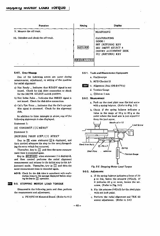
I.Cf.lf.lIIIY IVIU1:ur Loau I orque
Function
9;' Measure the off track.
10. Calculate and check the off track.
5-4-7. Error Message
One of the following errors can occur during measurement: adjustment, or setting of the machine for radial alignment:
a) Not Ready ... Indicates that READY signal is not issued. Check for disk drive connection or check for the DRIVE SELECf switch position.
b) Not Index Pulse ... Indicates that INDEX signal is not issued. Check for disk drive connection.
c) Cat's Eye Error ... Indicates that the Cat's eye pat· tern signal is abnormal. Check for the alignment ~~ ,
In addition to these messages in above, one of the following statements is also displayed.
Statement I:
[0] CONTINUE / [I] RETRY
Statement 2:
[RETURN] FIRST STEP / [I] RETRY
Key in [Q] when statement [] is displayed, and then control advances the step to the next,disregard. ing the error which has occurred.
Thereafter, key in. ill and then the same measure· ment item is executed again.
Key in IRETURNI when statement 2 is displayed, and then control performs the radial alignment measurement and returns to the initial step in the Ad· justment mode. Thereafter, key in ill and th~n the same measurement item is executed again.
NOTE: Check for the disk drive in accordance with COnfll·
mation items to the message displayed before retry· ing the key·in [] operation.
m 5-5. STEPPING MOTOR LOAD TORQUE
Disassemble the following parts and then perform the measurement and adjustment.
a. FC-9/FC-14 Mounted Board. (Refer to 4-1)
Keying Display
-46-
MEASURING
CALCURATING GOOD! HIT [RETURN] KEY SET DRIVE SELECf 4 INSERT AUGNMENT DISK HIT [RETURN] KEY
5-5-1. Tools and Measurement Equipment
a. Oscilloscope
b. MFD Checker II
_ c. Alignment Disk (OR·D47VA)
d. Tention Gauge
e .. ®Driver 2 mm
5-5-2. Measurement
a. Push up the steel plate near the lead screw with a spring balance. (Refer to Fig. 5-5)
b. Check if the spring balance indicates a value in the range of SO g to 80 g at the point where the head arm is just separated from the lead screw.
Fig. 5-5 Stepping Motor Load Torque
5-5-3. Adjustment
a. If the spring balance indicates a force of SO g or less, fasten the setscrew (+P2x3). If it indicates 80 g or more, loosen the set· screw. (Refer to Fig. 5-5)
b. Fix the setscrew (+P2x3) for the steel plate with nut lock paint.
c. Perform the radial alignment and TRK 00 sensor adjustment. (Refer to 5-4)
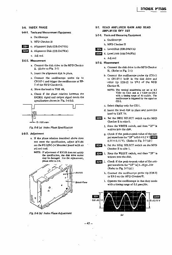
5-6. INDEX PHASE
5-6·1. Tools and Measurement Equipment
a. Oscilloscope
b. MFD Checker II
lED c. Alignment Disk (OR·D47VA)
ED d. Alignment Disk (OR·D47WA)
e. Adj rod.
5·6·2. Measurement
a. Connect the disk drive to the MFD Checker n. (Refer to Fig. 2·1)
b. Insert the alignment disk in place.
c. Connect the oscilloscope probe tip to eNl07·l and trigger the oscilloscope at TP· 5 of the MFD Checker II.
d. Move the head to TRK 40.
e. Check if the phase relation between the INDEX signal and output signal meets the specification shown in Fig. 5-6 (a).
I
j~ Fig. 5·6 (a) Index Phase Specification
5-6·3. Adjustment
a. If the phase relation described above does not meet the specification, adjust RVlOl on the FC-9/FC-14 Mounted Board with an adj rod tool.
NOTE: If adjustment of RVI0l does not satisfy the specification, the disk drive motor may be damaged. For the replacement, please refer to 5·8.
RV101
Shield Plate
Fig. 5·6 (b) Index Phase Adjustment
-47-
Inaex t'nas
5·7. READ AMPLIFIER GAIN AND READ AMPLIFIER OFF SET
5·7·1. Tools and Measuring Equipment
a. Oscilloscope
b. MFD Checker II
Em c. Level Disk (OR·D46VA)
IE d. Level Disk (OR·D46WA)
e. Adj rod
5-7·2. Measurement
a. Connect the disk drive to the MFD Checker II. (Refer to Fig. 2-1)
b. Connect the oscilloscope probe tip (CH-l) to CNI07-l built in the disk drive and other tip (CH·2) to TP-5 of the MFD Checker II.
NOTE: The vertical sensitivities are set at 0.2 V/div on CH·l and at 2 V/div on CH·2 with a timing range of 10 ms/div. The oscilloscope is triggered by the signal on CH·2.
c. Select display only for CH·}'
d. Insert the level disk in place and move the head to TRK 79.
m e. Set the SIDE SELECT switch on the MFD Checker IT to side O.
f. Press the WRITE switch, and then "2F" is written into the disk.
g. Check if the peak.ta-peak value of the output waveform for "2F" is 0.6 ± 0.2 V (Em 0.35 ± 0.15 V). (Refer to Fig. 5-7 (a) )
m h. Set the SIDE SELECT switch on the MFD Checker IT to side 1.
m i. Press the WRITE switch, and then "2F" is written into the disk.
m j. Check if the peak-ta-peak value of the output waveform for "2F" is 10. 3S±O .1SV
(Refer to Fig. 5-7 (a) )
k. Connect the oscilloscope probe tip (CH·2) to TP-3 on the MFD Checker II.
L Operate the oscilloscope in the chop mode with a timing range of 0.5 IJ.sec/div.
m to.15 V
(a)
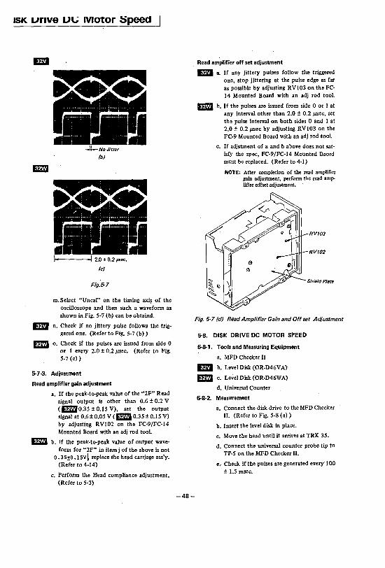
15K urlve Ul; Motor ~peed
(b)
(e)
Fig. 5-7
m. Select "Uncal" on the timing axi~ of the oscilloscope and then such a waveform as shown in Fig. 5-7 (b) can be obtaind.
Em n. Check if no jittery pulse follows the triggered one. (Refer to Fig. 5-7 (b»
e o. Check if the pulses are issued from side 0 or I every 2.0 ± 0.2 p.sec. (Refer to Fig. 5-7 (c»
5-7-3. Adjustment
Read amplifier gain adjustment
a. If the peak-to-peak value of the "2F" Read signal output is other than 0.6 ± 0.2 V (BO.35±0.15V), set the output signal at 0.6±0.05V (e 0.35±0.15 V) by adjusting RVI02 on the FC-9/FC-14 Mounted Board with an adj rod tool.
EI b. If the peak-to-peak value of output waveform for "2F" in itemj of the above is not
o • 35:!:O .15V~ replace the head carriage ass'y. (Refer to 4-14)
c. Perform the Head compliance adjustment. (Refer to 5-3)
-48-
Read amplifier off set adjustment
ED a. If any jittery pulses follow the triggered one, stop jittering at the pulse edge as far as possible by adjusting RVI03 on the FC-14 Mounted Board with an adj rod tooL
ED b. If the pulses are issued from side 0 or I at any interval other than 2.0 ± 0.2 p.sec, set the pulse interval on both sides 0 and I at 2.0 ± 0.2llsec by adjusting RVI03 on the FC-9 Mounted Board with an adj rod tooL
c. If adjstment of a and b above does not satisfy the spec, FC-9/FC-14 Mounted Baord must be replaced. (Refer to 4-1)
NOTE: After completion of the read amplifier gain adjustment, perform the read amplifier offset adjustment.
RV103
RV102
Shield Plate
Fig. 5-7 (d) Read Amplifier Gain and Off set Adjustment
5-8. DISK DRIVE DC MOTOR SPEED
5-8-1. Tools and Measuring Equipment
a. MFD Checker II
ED b. Level Disk (OR-D46VA)
e c. LevelDisk (OR-D46WA)
d. Universal Counter
5-8-2. Measurement
a. Connect the disk drive to the MFD Checker II. (Refer to Fig. 5-8 (a) )
b. Insert the level disk in place.
c. Move the head until it arrives at TRK 35.
d. Connect the universal counter probe tip to TP-5 on the MFD Checker II.
e. Check if the pulses are generated every" 100 ± 1.5 msec.
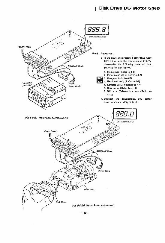
Fig. 5·8 (a) Motor Speed Measurement
/
Disl< Drive U{; .Vlotor :::»peel
5-8-3 Adjustment
a. If the pulses are generated other than every 100±1.5 msec in the measurement (5-8-2), disassemble the following parts and then perform the adjustment.
1. Main cover (Refer to 4-5) 2. Front panel ass'y (Refer to 4-2)
EmJ 3. Damper (Refer to 4-7) m 4. Head load ass'y (Refer to 4-8) 5. Cassette-up ass'y (Refer to 4-9) 6. Disk motor (Refer to 4~11) 7. WP arm, D-Detection arm (Refer to
4-10)
b. Connect the disassembled disk motor board as shown in Fig. 5-8 (b).
Fig. 5-8 (b) Motor Speed Adjustment
-49-
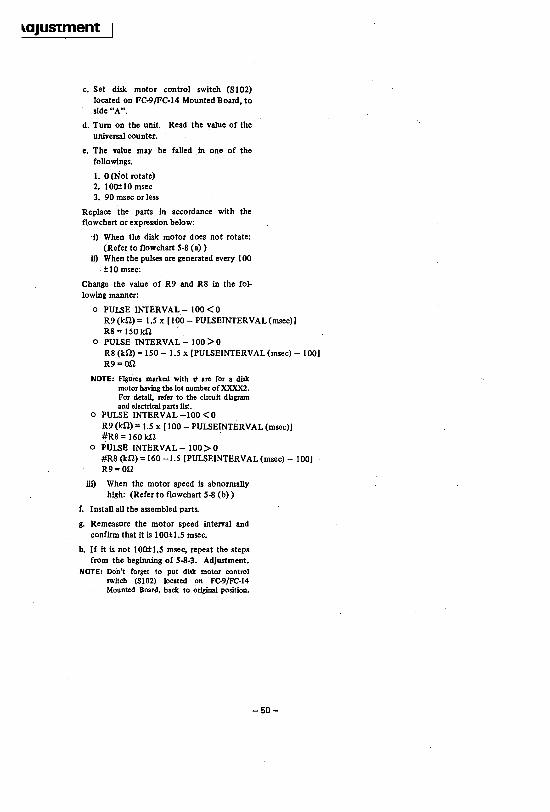
~aJustment
c. Set !llsk motor control switch (SI02) located on FC-9/FC-14 Mounted Board, to side "A".
d. Tum on the unit. Read the value of the universal counter.
e. The value may be failed in one of the followings.
1. 0 (N ot rotate) 2. 100±10 msec 3. 90'msec orless
Replace the parts in accordance with the flowchart or expression below:
'0 When the disk motor does not rotate: (Refer to flowchart 5-8 (a»
ii) When the pulses are generated every 100 . ±IO msec:
Change the value of R9 and R8 in the following manner:
o PULSE INTERVAL- 100<0 R9 (kil) = 1.5 x [100 - PULSEINTERV AL (msec)] R8 = ISOkil .
o PULSE INTERVAL- 100>0 R8 (kil) = ISO - 1.5 x [PULSElNTERVAL(msec) - 100] R9 = Oil
NOTE: Figures marked with # are for a disk motor having the lot number of XXXX2. For detail, refer to the circuit diagram and electrical parts list.
o PULSE INTERVAL -100 <0 R9(kil)= 1.5 x [100 - PULSEINTERVAL(msec)] :/tR8 = 160 kil .
o PULSE INTERVAL-IOO>O #R8 (kil) = 160 -1.5 [PULSEINTERVAL(msec) - 100] R9 = Oil
iii) When the motor speed is abnormally high: (Refer to flowchart 5-8 (b»
f. Install all the assembled parts.
g. Remeasure the motor speed interval and confirm that it is 1 OO± 1.5 msec.
h. If it is not 100±1.S msec, repeat the steps from the beginning of 5·8·3. Adjustment.
NOTE: Don't forget to put disk motor control switch (SI02) located on FC·9/FC·14 Mounted Board, back to original position.
-50-
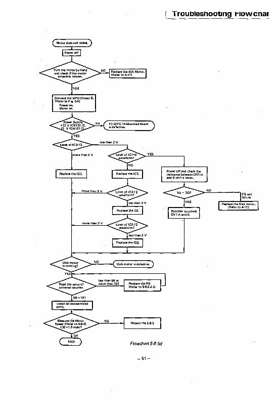
FC·9/FC·14 Mounted Board Iidotoctl ...
Repeat the 5-8-3
Flowchart 5-8 (a)
-51-
Troublesnootlng t".owcnar
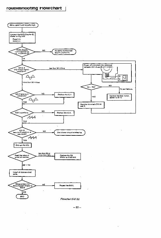
rouDlesnootlng· t-IOWchart
FC·9/FC·14 Mounted Board is defective.
less than 50 mVp-p
Disk Motor circuit i. defectill8.
Replace the R9. (Refer to 5-8-3 d·1I)
Repeat the 5-8-3,
Flowchart 5-8 (b)
-52-
Power off and check the resistance -"",.,,,,,,,.;" " ... ,. ~ L-..-.r--.~
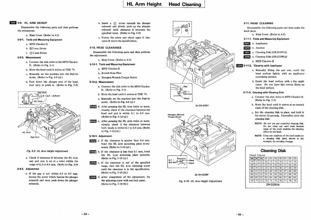
Em 5·9. HL ARM HEIGHT
Disassemble the following parts and then perform the adjustment.
a. Main Cover (Refer to 4·5)
5·9·1. Tools and Measuring Equipment
a. MFD Checker II
b. <±> 2 mm Driver
c. e 2 mm Driver
5-9~2. Measurement
a. Connect the disk drive to the MFD·Checker II. (Refer to Fig. 2·1)
b. Move the head until it arrives at TRK 79.
c. Manually set the machine into the Disk·In mode. (Refer to Fig. 4·9 (a»
d. Push down the plunger core of the head. load ass'y at point A. (Refer to Fig. 5·9)
Pad Arm
~'B~O'3-0'9mm HLArm
;:
Fig. 5·9 HL Arm Height Adjustment
e. Check if clearance B between the HL Arm and pad arm is set at a value within the range of 0.3 to 0.9 mm. (Refer to Fig. 5-9)
5·9·3. Adjustment
a. If the gap is not within 0.3 to 0.9 mm, loosen the screw which fastens the plunger solenoid and once push down the plunger solenoid.
-53-
Hl Arm Height
b. Insert a e driver beneath the plunger solenoid and slowly push up the plunger solenoid until clearance B becomes the specified value. CRefer to Fig. 5-9)
c. Fasten the screw and check again if clearance B meets the specification.
5-10. HEAD CLEARANCE
Disassemble the following parts and then perform the adjustment.
a. Main Cover (Refer to 4-5)
5·1()-1. Tools and Measuring Equipment
a. MFD Checker II
b. Round Nose Plier
c. Hexagon Wrench Torque Driver
5-10·2. Measurement
a. Connect the disk drive to the MFD Checker II. (Refer to Fig. 2-1)
b. Move the head until it arrives at TRK 79.
c. Manually set the machine into the Disk-In mode. (Refer to Fig. 4-9 (a) )
fD d. After pressing the HL Arm twice or morc, visually check if the clearance between the head and pad is within 0.1 to 0.4 mm. (Refer to Fig. 5-10 Ca»
_ c. After pressing the HL Arm twice or morc, visually check if the clearance between both heads is within 0.1 to 0.4 mm. (Refer to Fig. 5-IOCb»
5·1()-3. Adjustment
II:Eri a. If the clearance is greater than 0.4 mm, bend the HL Arm mounting plate downwards. CRefer to 5·10 Ca»
m b. If the clearance is less than 0.1 mm, bend the HL Arm mounting plate upwards. CRefer to F;g; 5-10 Ca»
mllI c. If the clearance is out of the specified range, turn the HL Arm adjusting screw until the clearance is in the specification. CRefer to Fig. 5-10 (b»
m d: After completion of the adjustment, fix the adjusting screw with nut lock paint. (Refer to Fig. 5-10 (b»
Head Cleaning
raIOA·D32V
fbi OA·D32W
Fig. 5·10 HL Arm Height Adjustment
5·11. HEAD CLEANING
Disassemble the following parts and then make the head clean.
a. Main Cover CRefer to 4·5)
5·11·1. Tools and Measuring Equipment
I!m a. Applicator
mz:I b. Alcohol
lim c. Cleaning Disk COR·D29VA)
m d. Cleaning Disk (OR-D29WA)
e. MFD Checker II
ID 5·11·2. 'Cleaning with Applicator
a. Manually lifting the pad arm, scrub the head surface lightly with an applicator containing alcohol.
b. Scrub the head surface with a dry applicator. Do not leave fine cotton fibers on the head surface.
5·11·3. Cleaning with Cleaning Disk
-54-
a. Connect the disk drive to MFD Checker II. CRefer to Fig. 2-1)
b. Move the head until it arrives at an unused track of the cleaning disk.
c. Set the cleaning disk in place, and hold it for about 10 seconds. Thereafter, eject the cleaning disk.
NOTE: Do not use any scratched cleaning disk. Do not reuse any used track because reuse of the track weakens the cleaning effect on the head.
NOTE: Cross out numbers of the used tracks on a cleaning disk label, shown in the example, for avoiding reusage.
Cleaning Disk Check Column .J;t! I]:J« 1.1'< 03 04 05 06 07 08 09
10 11 12 13 14 15 16 17 18 19 20 21 22 23 24 25 26 27 28 29 30 31 32 33 34 35 36 37 38 39 40 41 42 43 44 45 46 47 48 49 50 51 52 53 54 55 56 57 58 59 60 61 62 63 64 65 66 67 68 69 70 71 72 73 74 75 76 77 78 79
OR-D29VA
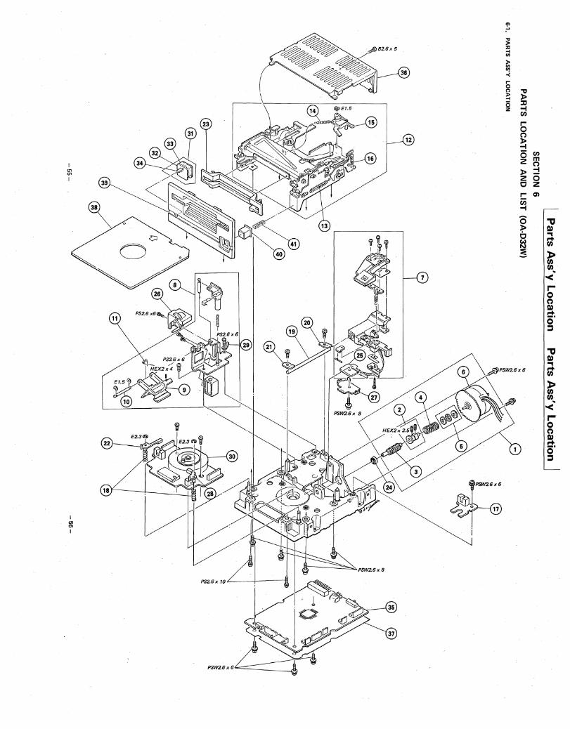
I U1 U1
I
I U1 Ol
I
11
PSW26 x 6'L-----">-'~
~ :ll
iii :I-en en -< r 0 n ~ (5 z
." » ::0 ..., (I)
5 (')
~ (5 (I)
z ~ » ::! z 0 c z !: en (I) ...,
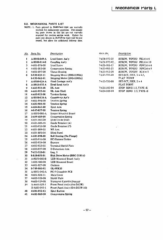
6-2. MECHANICAL PARTS LIST NOTE: 1. Parts printed in Bold·Face type are nonnally
stocked for replacement purposes. The remain-ing parts shown in this list are not nonnally required for routine service work. Orders for parts not shown in Bold·Face type will be pro-cessed, but allow for additional delivery time.
No. Parts No. Description
A-8010·049-A Lead Screw Ass'y 2 A-8010-014-B Coupling Ass'y 3 4-601-076-00 Lead Screw 4 4-601-083-00 Compression Spring
4-601-097-00 Thrust Bearing 6 8-838-025-11 Stepping Motor (SNS-II OOA)
8-838-061-01 Stepping Motor (SNS-1500A) 7 A-8010-024-A Head Carriage Ass'y 8 A-8010-025-A Head Load Ass'y
9 4-603-921-00 HLArm 10 4-603-922-00 HL Arm Shaft 11 4-603-923-00 Torsion Spring 12 A-80 10-026-A Cassette-up Ass'y 13 4-601-096-00 Tention Spring 14 4-603-901-00 Tension Spring IS 4-604-062-00 Eject Arm 16 4-847-057-00 Tension Spring 17 A-8050-001-A Sensor Mounted Board 18 3-659-609-00 Compression Spring 19 4-601-003-00 Slide Guide Shaft 20 4-601-008-03 Guide Retainer (A) 21 4-603-926-00 Guide Retainer (C) 22 4-601-009-03 WPArm 23 4-601-050-04 Blind Panel 24 4-601-098-00 Ball Bearing (No Flange) 25 4-603-916-00 HC-Harness Holder 26 4-603-924-00 Damper 27 4-603-925-02 Terminal Shield Plate 28 4-603-927-00 D-Detection Arm 29 7-623-520-01 Lug, 3 30 8-838-050-01 Disk Drive Motor (BHC-210IA) 31 A-8050-002-B LED Mounted Board Ass'y 32 1-605-400-00 LED Mounted Board 33 4-601-027-00 Cushion 34 8-719-900-92 GL-9PR20 35 A-805l-042-A FC-9 Complete PCB 36 4-601-026-11 Main Cover 37 4-603-928-00 Shield Plate 38 4-603-929-00 Transport Cassette Dummy 39 X-4601-029-1 Front Panel Ass'y (OA-D32W)
X-460l-043-1 Front Panel Ass'y (OA-D32W-lO) 40 4-601-052-12 Eject Button 41 4-601-060-00 Compression Spring
-57-
Parts No.
7-621-972-25 7-621-972-4~, .. 7-621-981-15 7-621-981-25 7-621-912-20 7-621-731-08
7-621-733-08
7-624-102-04 7-624-105-04
IVlecnanlcal ~arts L
Description
SCREW, TOTSU PS2.6 x 6 SCREW, TOTSU PS2.6 x 10 SCREW, TOTSU PSW2.6 x 6 SCREW, TOTSU PSW2.6 x 8 SCREW, TOTSU B2.6 x 5 SET-SCT, HEX. 2 x 2.5, FLAT POINT SET-SCT, HEX. 2 x 4 FLAT POINT STOP RING 1.5, TYPE-E STOP RING 2.3, TYPE -E

MEMO
........................................ ~ ................................................................................................................................................................... .
.............................................................................................................................................................................. : .............................. .
•• 0 ••••••• 0 ••• 0 ••••••••••• 0 '0' ...... ~ ••••••••••••••••••• 0 •••••••••••••••••••••••••••••••••••••••••••••••••• 0 •••••••••••••••••••••••••••••••• 0 ••• 0 •• 0 .......................................................... .
............................................................................................ : ................................................................................................................ .
-58-
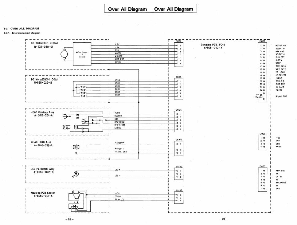
Over All Diagram Over All Diagram
6-3. OVER ALL DIAGRAM
6-3-1. Interconnection Diagram
r-----I 1 I 1
DC MotorIBHC-210IA)
B- B3B-050-01
-------------1 I
CNIOI +12V +5V GND MOTON
1 Mo'tor Servo
a Senser MINDEX I
I ~ ________ +-~W~R~T~P~R~T ________________________ ~ __ ~ 6
CSTI N 5 I I L..... _________ _
r - - - - - - - - -_-I DC MotorlSNS-11 OOA) 1 B-B3B- 025-11
I I I I
------------- 1
------------- -, I I
~ I
I~ I I
-~ I -vv' I
1 - - ----------L ___________ _
r - - - -. - - - - - - -------------, I HEAD Carriage Assy 1
-lP-< I
1 I
-~ J. I
I . A-BOIQ-024-A
I I
X X~ I
I . I L ___ _ ____________ ...1
r--------- - - - - - - - - - - --., I HEAD LOAD Assy I
~ I I I I 1 --.--:---- ----:-,.--
I A-BOIO-032-A
1 I I L __ :- __
r------------- ---------, I LED PC BOARD Assy
SMC¢ SMCI SMAI 5MBI SMA2 5MB2
HCOM I HCDM¢ GND R/W ANISH R/W START ERASE
PJun er rI>
Plung-er I FRAME GND
LEO+ I A-B050-002-B I I ~~~--------~~~~----------------~ I
LED-
L ___ _ ----------------~
~ I 2 5 6 4 3
'---
~ I 2 3 4
5
6 '---
~ 3
2 I ~
CNI02
~ r - - - - - -- - - - - - - - - - - - - - - -l CNI03
I Mounted PCB Sensor 3 4 +-__ ~ ______ -+I __ -;T:;5~V;;:_------------------------_;:__t~ I A-8050-001-A 4------+I-..,;C~T~::¢7.:::__----------_;___t-c I r---------~I---~TR~¢~~~D~----------------------_TI--f_O
I I I I I
Complete PCB, FC-9 A-B051-042 -A
- - - - - --CNI091
I 0 2 0 3 0 4 0 5 0 6 0 B 0 100 120 140 160 180 200 220 240 260
7-25 ? 10dd N.I'
0
[illC~I: 2 0 3 0 4 0
CNI07
10 2 0 3 0 4 0 5 0 6 0 7 0
I I 2 ~ ~ _________________ . ___________ --l L ____________ ~ ________ _
-59- -80-
MOTOR ON SELECT ¢ DSK CHG SELECT 4 CHG R5T OIRTN STEP WRT DATA WRT GATE HJl LOAD HD SELECT INDEX TRK'¢¢ WRT PRT RD DATA READY
Signal GND
+5V GND GND +12V
AMP OUT NC CSTIN NC TRK¢SNS NC GND
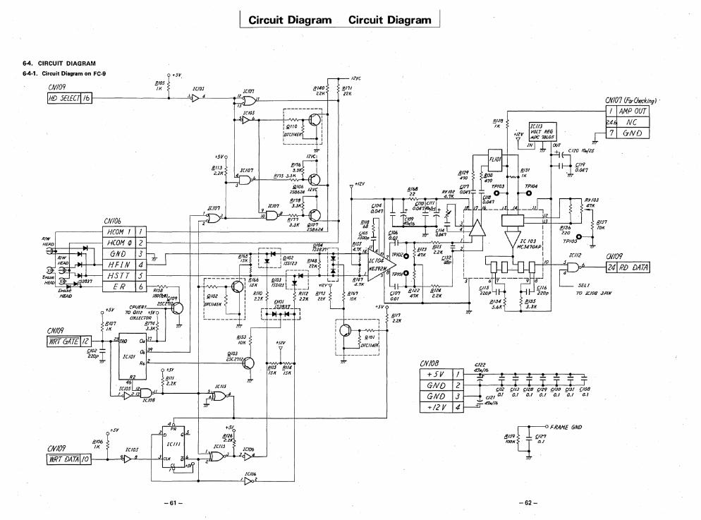
6-4. CIRCUIT DIAGRAM
6-4·1. Circuit Diagram on FC·9
BIOJ IX
Circuit Diagram
8140 ZZX
16~----------~~~~--~~~ __________ ~ '--_----'L.....J
eNI06
t5V
8107 II(
flOZ T 2lOp ,;,.
;~~i:l-t-:j"r-,--.-ti COllECTOR
lP74 .] • .]J(
-61-
t5V
8/1J Z.ZK
ICl07
r---------, I
RIlJ RI/4 lSI( lSI(
Circuit Diagram
leye
11171 elK
Jill7 2.2K
(N108
+5V !
!!Jl~ IX
eNI07 (ForCheckfngJ
r---------------~I AMP OUT .4. NC 7 aND
GND 2 1---+--__ --_-*--+----">----::-'
GND J +/2V 4
EF FI?AHE GND
tflS9 fIn lOON 0-1
-62-
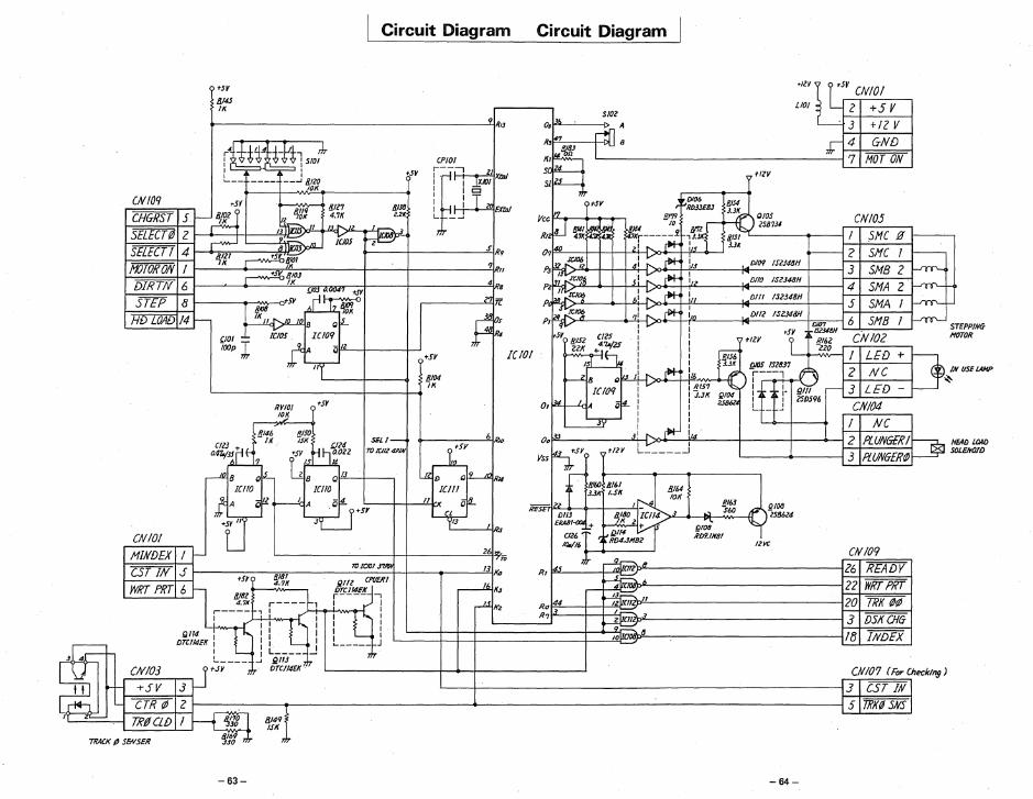
! \I , 2
TRAC/(
Circuit Diagram
-SV
814S IX
RIJ
(llirfitti l510f CPlOI I , +sv r-,~ L __ , XfA/
---- __...J !lIZO f ,m 10K
i ~JL CNI09 I I .SY lill? 81J8 I I
CHGRST S~~ " 4ifi EXW
4.?X Z.ZK L _~
/pl /31--.." I irc.Mpl.; SELECT@ 2 ~ ~: [C/OJ z= IJ IIElID""- SR. SELECT I 4 4121 '5y':~
!1OTORON 1 X ? /I
~BIOJ DIRTN 6 IX 4. •
~ STEP z? Tt 8 tSY
~ ~ HDLOAD !4 P Os r- I B o~
ClOI ICiOS 1009 R4
lOOp I tA O'Z IUO/ .sv
T 8104 IX
RYIOI 'Sf
IOJ!
8146 RISO 6 R", IX lSI( "24 SEl/-
CIZ3~ 'SY a4?jJJ 1 'SY ~02Z TO lCIlZ 4PIN
[/ 14 ~B oiL 2 B Q 13 gD oiL-" R14
1CIIO !CliO 1C/II
Circuit Diagram
.llV'Y .SV CNlO! LlOI ~ 2 +5 V 5102
O • .lh A '--'- 3 +12 V R.·? -t±O B + 4 GND J( 8J~ I 7 MOT ON
~~ 'i tlZV
~~~EB.J 81J4 _Sy , ~QIOS Vee 7 8m eN!OJ
~ ~ 10 258131 ~(fJ41 8/U ,:~ RI2 411. fC;Xr----- i 8.1S1 1 ~I1C ff
7 1 " r* i,! 3JK 07 40
4i v .PO+-~ '2 SI'1C ,
ICI06 IIJ i3~' DlIJ'l ISZ.J4lJH
3 5MB 2 ~
I
Pzrhlf18 SI !12 DI/O ISZJ48H 4 SMA 2
1 ICI06 I ~
A~~ b! "-I Dill IS2348H I 5 SMA ,
I 1* I
ql "- 1m DIIZ ISlJ4&H 6 5118 1 PI DID? IV I ISZJ48H
Sf 81S2 Cl2S I l CNIOZ I tlZY 816Z zzx +4.'11/25 I Z20 LED ,L.:.:.....l! I fJ6 I +
I JK QIOS IS2837 H> i'*" 1/6 Z NC W8 Q~ r---l
/ClO9 ! 8 157 01";; ifrt - 3 LED -
J.3X I I' Bill OIJ£.~A 014- 2586Z< I I 2SD.S96
CN!04 L _ J
L...'::::2Y r* 114
I NC 00 33 "- PLUNGER! I
, 2 ~sv fUV L -l
3 Pf.UNGER¢ VSS
33X 151( !l164 •• 10J( R16'J
I---
f-rn'-..,..,.
f-rrr'-f-rrr'- 5 TEPPING
'!lTOR 11<
[J/N ~ IJSE l.AHP
'EIID llJAD lENOID ~~
P"~' ~ fA ,,~ ~A o~ II J( o~ 22 ,_ ~,~ +SY
~ RES,.
DI17, ...... ~'3 560 lSB6Z4 ..,
.... sr 11 3 ERA81 + /1( 2 + D';; :r Cll6 ,,'d:/:.3HBZ iDVH81 (NIDI
10./16 IZve
I1INDEX 1 I- 26 'Y';;; (NI09 17)ICJOI,J7Rh
13 0 45_ " ~" Z6 READV CST Jft( ,J H, tSf KIIlI CPIIE!?! ~6 WRT PRT 6
4.7K QIIZ ----1f> f(, 22 WRTPRT DTCI14EK
1i182 r----~l r---- ..., ~/(z ~" 20 TRJ( ¢¢ 4.7K I I Ro 44 I r---- , I
~3 I I I I R7 3 DSJ(CHG I I I I I
D~:!~Ef( I I I I I I 10 6 I I 16 JNDEX I I I L _____ J
I ..J I I L ____
Jr~Y--- ...J ~113
(ft(103 DTCII4EX CNI07 (For Checking)
-r,JV J 3 CST IN CTR¢ 2 5 lRJ({! SNS
TRDCLD 1 ~ 8/411 ISX
SENSER 8j69 30
-63- -64-
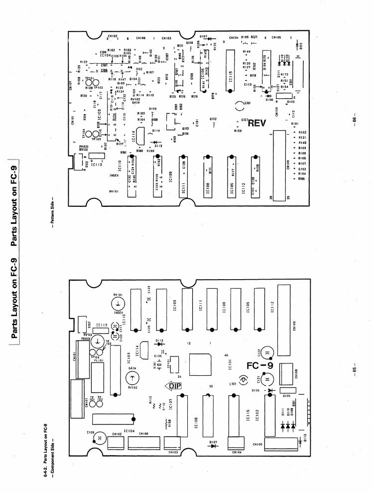
en I
0 LL C 0 .... ::l 0 > CIS
...I
~ CIS
0..
en I
0 LL C 0 .... ::l 0 > CIS
...I
J!) ... CIS
0..
" :5!
'" E " :: J! I
~ S s o .. j~ E i l. R
• E
l 8
... o z u
eNI02 3 I CNI06 CNID3
RI62 + RI66 + N C104 RI65 ~ £ ,...
I RI71
I -~ 1 It a;~
+ ICI04r05RI55., +.. 0 00 !!!
RI22 J ~ .......... ~ .......... ~a ....... :!
.. + CtDl + + ~' N I ~ ~ ...
+ --= J<.lQ§. =- .=j-~ } + RIS7 ~;,J j. -
CD ~Ol RI18 RI4' 0104 0 + ~ :;:;;: u:. I ~ + U 0103...-.- + c~ a: ~..........,
RI29 TPI02 + RI25 ... I f 1RI24 ~ + - + R130' + += 0 ~ a:RIU RIIS
u t=f<C'-i:j RVI02
'" =+ ~ I = GAIN
a:+lru 0108
RI75 R176
~5 "' o
~ + §/ ~
u
RI63
RIG4 r 0108
fit t
DI*-
n110 m
f1~ ~~l;'~ ~ ~a: _ u
u -t ; +
'" ;!' 0; Rl78
+!! om o
z u ~----+-i+ +1
~Od-'I+ +I ~D } 0114 .....
I ...... L....; 0113
u T ......0114
to- TPI03 I, _
PHASE RVIOJ
+:! '"
N D I lJ '" c::=J
I} ICI13
RI::!!:,j
INDEX
-+I-0113
1180 RISO
+~
0> o
~
+ +I
RVIOI
o " INDEX
l J~ ICI13 C~'1J RVI03c::=J fl.."
PHASE(";\ \..:::::)~
IJ~T~3 "
C C1 -: 1PI04 I I .,
l[ 0
... Mt lh §u0
I +
.. N
U
::::: ~ N
U
~D
~
0113-
-+!-
'" o
CI2SlI '_[J .L 0
0= <i:L - U x, 24
<9IPJ - '"" ~ ~ ~~ ~
f~ Clo0c::iT4 CNIOS I
m N
U
~
12
t ~
<Xl o
~
o ID o
~
3S
0107
-+!-
<Xl o
••
CNIO", 0105 ntH CNI05
... '"
<n o
~
I ........... fg RI.. n I=I~I ~. tCtCt RI20 ~ £
AI27 § c :: RI72
...... c + + R119 RI51 E
+ ., + -[;; RIS4 C113~ cr + _
;;; ~"* c:=JE ,,",LtDI
0106 BOlOS
'-.J
+ C127REV +
RI59
~
<n o
'" +E
'" ~+ U
let IU
~ N
~W u'C.J
'" o z u
N
+ = U
m
RIOI
+ RI02
+ RI21
+ RI .. 5
+ RIO!
+ RIDB
+ RIDS
~ + RI07 z u + CI02
~ N
+ RIO ..
+ 8105
m o z u
LlDI
FC-Q D ~ 28 ~
DIOS -~ c=J 0105
N o ~'" om __ 0
o 00
ii I I
CNIDSI It ~
<D <D
I
on <D I
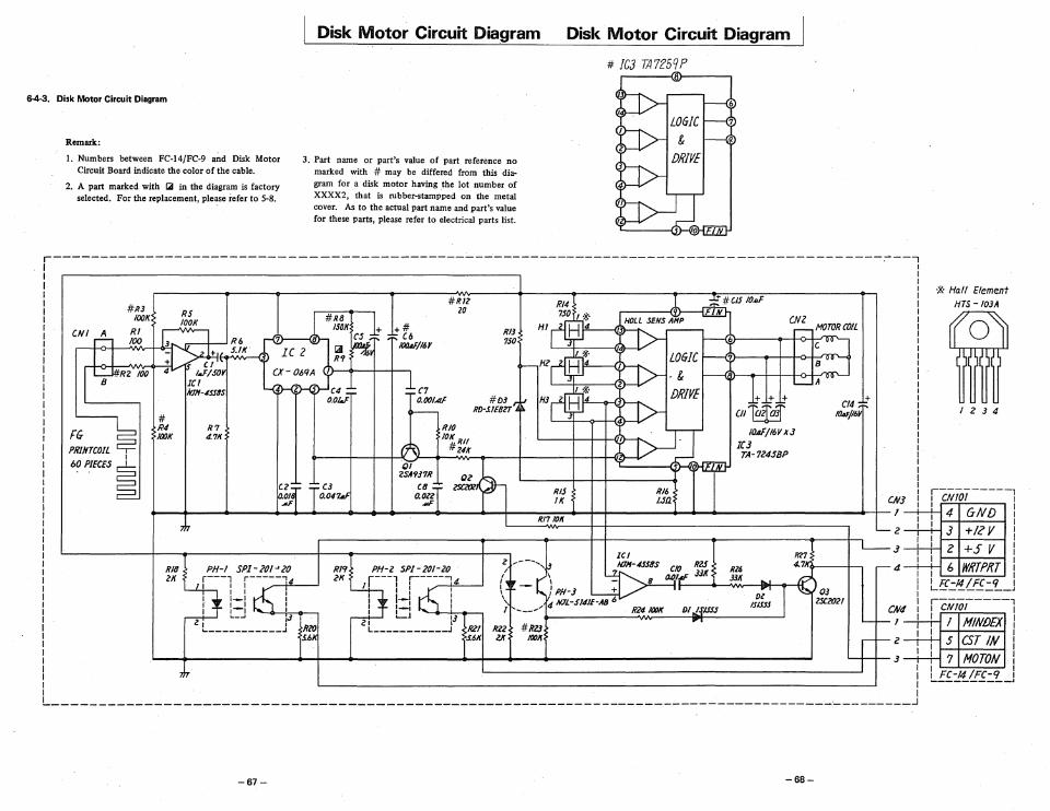
6-4-3_ Disk Motor Circuit Diagram
Remark:
1. Numbers between FC-14/FC-9 and Disk Motor Circuit Board indicate the color of the cable.
2. A part marked with 14 in the diagram is factory selected. For the replacement, please refer to S-8.
Disk Motor Circuit Diagram
3. Part name or part's value of part reference no marked with # may be differed from this diagram for a disk motor having the lot number of XXXX2, that is rubber-stampped on the metal cover. As to the actual part name and pares value for these parts, please refer to electrical parts list.
Disk Motor Circuit Diagram
# IC3 TA7259P
r------------------------------------------------------------------------------------------1
#RJ lOOK
RI 100
r;---L P';NTCOIL ~ 60 PIECES ~
#
RS lOOK
R4 R7 lOOK 4.7K
C~/8rlCJ Io-~ o.on.J
RI9 lX
#RIl 20
"'3 7S0 "'ri~ j:;L -a£C"" H"~~ I LOGIC1=J7}---+-I-O-+:B,.rn--u<~
c~ MOTOR COIL
C' uu
~ I ljf I 1>-· & 1 L..- A UP
l~lK' 1 DRIVE + + + C''4 + #DJ ,ljt' H.J Z H H:f..,.. ,. RD-S.IEDlT'1" 4;»"- CII ~ to..F116~
RIO 10K RII
#UK
QI 2SA9J7R
PH-Z SP/-201-20 1 r---l r-----,4-
I l-iJ! : :-,ll I
21 L..-J lJ L ___________ ~ HZ!
:S;6X
RIS IK
I RI110K
1
RI6 lSa
liUIF/I6Y IfJ IC3 TA-7l4SBP
R27
Rl6 4.7.
.WI .. tV DZ
I ~
z ~----t;' ~~-4S!BS elO RZI (~, '. ~B o.Dle 3JK \ - J PH-) + .. !--............. "W'r--!i-r-...... -K. \ N.7L-S!4!E-AB 6 ! , ___ / 4 8.,4 /OIJI( D~.J
RlZ ZJ(
#RlJ 10011
~
ISID!
) 03 lSC2011
'-
L I
~
.-
t-
t-
2
.3
4
2
J
I I I I I I I I I I I
-----------------------------------------------------------------------------------------------~
-67- -68-
.,& Hall Element HTS - l03A
I 2 3 4
1(#TO'-----1 I
I 4 GND I 3 +121/
2 +5 V I 6 WRTPf(T LEI ~'i tfi:.'L_ r--------, I-CNIOI I
I 1 /1/NIJEX I I
5 CST IN I 7 MOTON I
I FC-/4IFC-9 I ..... _________ J
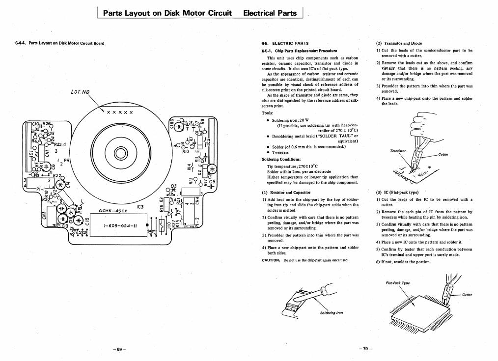
Parts Layout on Disk Motor Circuit
·6-4-4. Paris Layout on Disk Motor Circuit Board ,
LOT. NO
@
-69-
Electrical Parts
6-5. ELECTRIC PARTS
6-6-1. Chip Parts Replacement Procedura
This unit uses chip. components such as carbon resistor, ceramic capacitor, transistor and diode in some circuits. It also uses IC's of flat-pack type.
As the appearance of carbon resistor and ceramic capacitor are identical, destinguishment of each can be possible by visual check of reference address of silk-screen print on the printed circuit board.
As the shape of transistor and diode are same, they also are. distinguished by the reference address of silkscreen print.
Tools:'
• Soldering iron; 20 W (If possible, use soldering tip with heat-<:on
troller of 270 ± 10°C) • Desoldering metal braid ("SOLDER TAUL" or
equivalent)
• Solder (of 0.6 mm dia. is recommended.) • Tweezers
Soiderin,B Conditions:
Tip temperature; 270±IOoC Solder within 2sec. per an electrode Higher temperature or longer tip application than specified may be damaged to the chip component.
(I) Resistor and Capacitor
1) Add heat onto the chip-part by the top of soldering iron tip and slide the chip-part aside when the solder is melted.
2) Confmn visually with care that there is no pattern peeling, damage, and/or bridge where the part was removed or its surrounding.
3) Presolder the pattern into thin where the part was removed.
4) ~ace a new chip-part onto the pattern and solder both sides.
CAUTION: Do not use the chip-part again once used.
-70-
(2) Transistor and Diode
I) Cut the leads of the semiconductor part to be removed with a cutter.
2) Remove the leads cut as the above, and confirm visually that there is no pattern peeling, any damage andlor bridge where the part was removed or its surrounding.
3) Presolder the pattern into thin where the part was removed.
4) Place a new chip-part onto the pattern and solder the leads. '
(3) IC (Flat-pack type)
I) Cut the lea<!s of the IC to be removed with a cutter.
2) Remove the each pin of IC from the pattern by tweezers while heating the pin by soldering iron.
3) Confmn visually with care that there Is no pattern peeling, damage, andlor bridge where the part was removed or its surrounding.
4) Place a new IC onto the pattern and solder it.
S) Confmn by tester that each conduction between IC's terminal and upper port Is surely made.
6) If not, resolder the portion.
Cutter
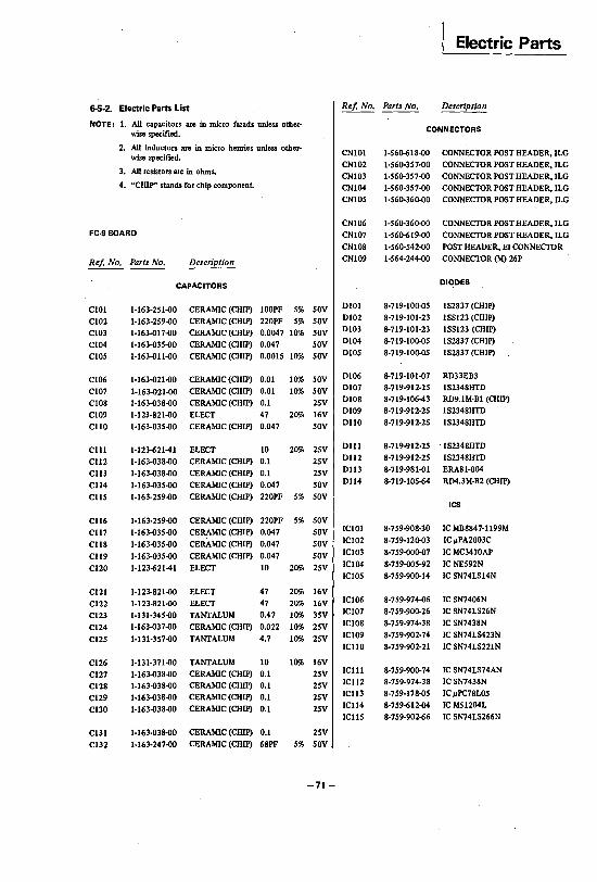
Electric Parts
6-5-2. Electric Parts List Ref. No. Parts No. Description
NOTE: 1. All capacitors are in micro farads unless other· wise specified. CONNECTORS
2. All inductors are in micro henries unless other-CNIOI wise specified.
1-56().61S-00 CONNECTOR POST HEADER. ILG
3. All resistors are in ohms. CNI02 1-560-357-00 CONNECTOR POST HEADER. ILG
CN103 1-560-357-00 CONNECTOR POST HEADER. ILG 4. "CHlP" stands for chip component CNI04 1-560-357-00 CONNECTOR POST HEADER. ILG
CN105 1-560-360-00 CONNECTOR POST HEADER. ILG
CNI06 1-560-360-00 CONNECTOR POST HEADER. ILG FC·9BOARD CNI07 1-56().6 I 9-00 CONNECTOR POST HEADER. ILG
CNI08 1-560-542-00 POST HEADER. EI CONNECTOR
Ref. No. Parts No. Description CNI09 1-564-244-00 CONNECTOR (M) 26P
CAPACITORS DIODES
CIOI 1-163-251-00 CERAMIC (CHIP) 100PF 5% 50V DIOI 8-719-100-05 IS2837 (CHIP)
CI02 1-163-259-00 CERAMIC (CHIP) 220PF 5% 50V DI02 S-719-101-23 ISSI23 (CHIP)
CI03 1-163-017-00 CERAMIC (CHIP) 0.0047 10% 50V DI03 8-719-101-23 ISSI23 (CHIP)
CI04 1-163-035-00 CERAMIC (CHIP) 0.047 50V DI04 8-719-100-05 IS2837 (CHIP)
CI05 1-163-011-00 CERAMIC (CHIP) 0.0015 10% 50V DI05 8-719-100-05 IS2837 (CHIP)"
CI06 1-163-021-00 CERAMIC (CHIP) 0.01 10% 50V DI06 8-719-101-07 RD33EB3
CI07 1-163-021-00 CERAMIC (CHIP) 0.01 10% 50V DI07 8-719-912-25 IS234SHTD
CI08 1-163-038-00 CERAMIC (CHIP) 0.1 2SV DI08 8-719-106-43 RD9.IM·BI (CHIP)
CI09 1-123-821-00 ELECT 47 20% 16V DI09 8-719-912-25 IS234SHTD
C110 1-163-035-00 CERAMIC (CHIP) 0.047 50V D110 8-719-912-25 IS2348HTD
C111 1-123-621-41 ELECT 10 20% 2SV Dill 8-719-912-25 "IS2348HTD
C112 1-163-038-00 CERAMIC (CHIP) 0.1 25V DI12 8-719-912-25 IS234SHTD
C113 1-163-038-00 CERAMIC (CHIP) 0.1 25V DI13 8-719-981-01 ERAS 1-004
C114 1-163-035-00 CERAMIC (CHIP) 0.047 50V D114 8-719-105-64 RD4.3M·B2 (CHIP)
C115 1-163-259-00 CERAMIC (CHIP) 220PF 5% 50V ICS
C116 1-163-259-00 CERAMIC (CHIP) 220PF 5% 50V
C117 1-163-035-00 CERAMIC (CHIP) 0.047 50V ICIOI 8-759-90S-30 IC MB8847-1199M
C118 1-163-035-00 CERAMIC (CHIP) 0.047 50V ICI02 8-759-120-03 ICI'PA2003C
C119 1-163-035-00 CERAMIC (CHIP) 0.047 SOV ICI03 S· 759-000-07 ICMC3470AP
C120 1-123-621-41 ELECT 10 20% 25V ICI04 8-759-005-92 ICNE592N
ICI05 8-759-900-14 IC SN74LSI4N
C121 1-123-821-00 ELECT 47 20% 16V
CI22 1-123-821-00 ELECT 47 20% 16V ICI06 8-759-974-06 IC SN7406N
C123 1-131-345-00 TANTALUM 0.47 10% 35V ICI07 8-759-900-26 IC SN74LS26N
CI24 1-163-037-00 CERAMIC (CHIP) 0.022 10% 25V ICI08 8-759-974-38 IC SN743SN
C125 1-131-357-00 TANTALUM 4.7 10% 25V ICI09 8-759-902-74 IC SN74LS423N
IC110 8-759-902-21 IC SN74LS221N
CI26 1-131-371-00 TANTALUM 10 10% 16V
CI27 1-163-o3S-00 CERAMIC (CHIP) 0.1 25V IC111 8-759-900-74 IC SN74LS74AN
C128 1-163-038-00 CERAMIC (CHIP) 0.1 25V IC112 8-759-974-38 ICSN7438N
CI29 1-163-038-00 CERAMIC (CHIP) 0.1 25V IC113 S· 759-178-05 ICI'PC78L05
C130 1-163-o3S-00 CERAMIC (CHIP) 0.1 25V IC114 8-759-612-04 IC M51204L
IC11S 8-759-902-66 IC SN74LS266N
CI31 1-163-038-00 CERAMIC (CHIP) 0.1 25V
C132 1-163-247-00 CERAMIC (CHIP) 68PF 5% SOV
-71-
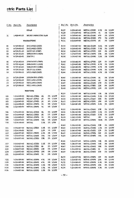
ctric Parts List
J1
01 02 03
04 05
06
07
08 09
10
11 ,12
113
114
LOI L02
L03
104 105
106 107 108 109
110
111 112 113 114
.115
.117
.118
~119
~120
~121
~122
t123
l124
1125 l126
Description
COILS
1-408-442-21 MICRO INDUCTOR 10IlH
TRANSISTORS
8-729-900-53 8-729-900-53 8-729-271-23 8-729-162-45 8-729-103-43
8-729-162-45
8-729-162-45 8-729-162-45
8-729-271-23 8-729-900-53
8-729-159-64 8-729-900-53
8-729-900-53 8-729-900-53
1-216-049-00 1-216-049-00
1-216-049-00 1-216-049-00
1-216-049-00
1-216-049-00 1-216-049-00 1-216-049-00
1-216-073-00 1-214-140-00
1-216-057-00 1-214-140-00 1-216-057-00 1-216-077-00 1-216-077-00
1-216-057-00 1-216-021-00
1-216-073-00 1-216-073-00 1-216-049-00
1-216-089-00
1-216-089-00
1-216-057-00 1-216-057-00
1-216-057-00
DTC114EK (CHIP) DTC114EK (CHIP) 2SC2712G (CHIP) 2SB624-BV5 (CHIP) 2SB734-2
2SB624-BV5 (CHIP) 2SB624-BV5 (CHIP)
2SB624-BV5 (CHIP)
2SC2712G (CHIP) DTC1l4EK (CHIP)
2SD596-DV5 (CHIP) DTC1l4EK (CHIP)
DTC1l4EK (CHIP) DTC1l4EK (CHIP)
RESITORS
METAL (CHIP) lK METAL (CHIP) lK
METAL (CHIP) lK METAL (CHIP) lK METAL (CHIP) lK
METAL (CHIP) lK METAL (CHIP) lK METAL (CHIP) lK
METAL (CHIP) 10K
METAL 2.2K
METAL (CHIP) 2.2K
METAL 2.2K METAL (CHIP) 2.2K METAL (CHIP) 15K METAL (CHIP) 15K
METAL (CHIP) 2.2K
METAL (CHIP) 68 METAL (CHIP) 10K METAL (CHIP) 10K METAL (CHIP) lK
METAL (CHIP) 47K
METAL (CHIP) 47K
METAL (CHIP) 2.2K METAL (CHIP) 2.2K
METAL (CHIP) 2.2K
5% 1/IOW 5% 1/10W
5% 1/10W 5% 1/IOW
5% 1/10W
5% 1/10W 5% 1/10W 5% 1/10W
5% 1/10W
1% 1/4W
5% 1/IOW 1% 1/4W 5% 1/10W 5% 1/10W
5% 1/IOW
5% 1/IOW
5% 1/IOW 5% 1/IOW
5% 1/10W 5% 1/IOW
5% l/lOW
5% I/lOW
5% 1/IOW
5% 1/10W 5% 1/10W
R127 R128 R129 R130 R131
R134 R135 R136 R137
R138
R140-
R141
R142
R143 R144
R145 R146
R147 R148
R149
R150
R151 RlS2 R153 R154
R155 R156
R157 R158 R159
R160
R161 R162
R163 R164
R165 R166
R167
R168 R169
R170
RI71
RI72 RI73
R174
-72-
Description
1-216-065-00 METAL (CHIP) 4.7K 1-216-049-00 METAL (CHIP) lK 1-216-041-00 METAL (CHIP) 470 1-216-041-00 METAL (CHIP) 470 1-216-049-00 METAL (CHIP) lK
1-216-067-00 1-216-061-00 1-216-033-00 1-216-073-00
1-216-057-00
1-216-081-00 1-216-065-00
1-2'16-065-00
1-216-065-00
1-216-065-00
1-216-049-00 1-216-049-00
1-216-083-00 1-216-081-00 1-216-077-00
METAL (CHIP) 5.6K METAL (CHIP) 3.3K METAL (CHIP) 220 METAL (CHIP) 10K
METAL (CHIP) 2.2K
METAL (CHIP) 22K METAL (CHIP) 4.7K
METAL (CHIP) 4.7K
METAL (CHIP) 4.7K METAL (CHIP) 4.7K
METAL (CHIP) lK
METAL (CHIP) lK METAL (CHIP) 27K METAL (CHIP) 22K METAL (CHIP) 15K
METAL (CHIP) 15K METAL (CHIP) 3.3K
5% 1/10W 5% 1/10W S% 1/10W 5% 1/10W 5% 1/10W
5% 1/10W 5% 1/10W
5% 1/10W 5% l/IOW 5% 1/10W
S% 1/10W S% 1/10W
5% 1/10W
S% I/IOW S% 1/10W
5% l/IOW
5% 1/IOW 5% l/lOW 5% 1/10W
5% 1/10W
1-216-077-00 1-216-061-00 1-216-081-00 1-216-073-00 1-216-061-00
METAL (CHIP) 22K S%
5% 1/10W 5% 1/10W
1/l0W 1/l0W 1/10W
1-216-083-00 1-216-061-00 1-216-061-00 1-212-S1S-00 1-216-097-00
1-216-085-00
1-216-053-00 1-216-033-00 1-216-043-00 1-216-073-00
1-216-077-00
1-216-077-00
1-216-073-00 1-216-009-00
1-216-037-00
1-216-037-00 1-216-081-00
1-216-061-00
1-216-08J-OO
1-216-061-00
METAL (CHIP) 10K 5% METAL (CHIP) 3.3K· 5%
METAL (CHIP) 27K METAL (CHIP) 3.3K METAL (CHIP) 3.3K METAL 180 METAL (CHIP) lOOK
METAL (CHIP) 33K
METAL (CHIP) I.SK METAL (CHIP) 220 METAL (CHIP) 560 METAL (CHIP) 10K
METAL (CHIP) ISK
METAL (CHIP) 15K METAL (CHIP) 10K
METAL (CHIP) 22
METAL (CHIP) 330
METAL (CHIP) 330 METAL (CHIP) 22K
METAL (CHIP) 3.3K
METAL (CHIP) 22K METAL (CHIP) 3.3K
5% 1/10W 5% 1/IOW
5% 1/10W 1% 1/2W 5% 1/IOW
5% 1/10W
5% 1/10W 5% 1/10W
5% 1/10W S% 1/10W
5% 1/10W 5% l/lOW
5% 1/10W 5% 1/IOW
5% 1/10W
5% 1/10W 5% 1/IOW 5% 1/10W
5% l/IOW
5% 1/10W
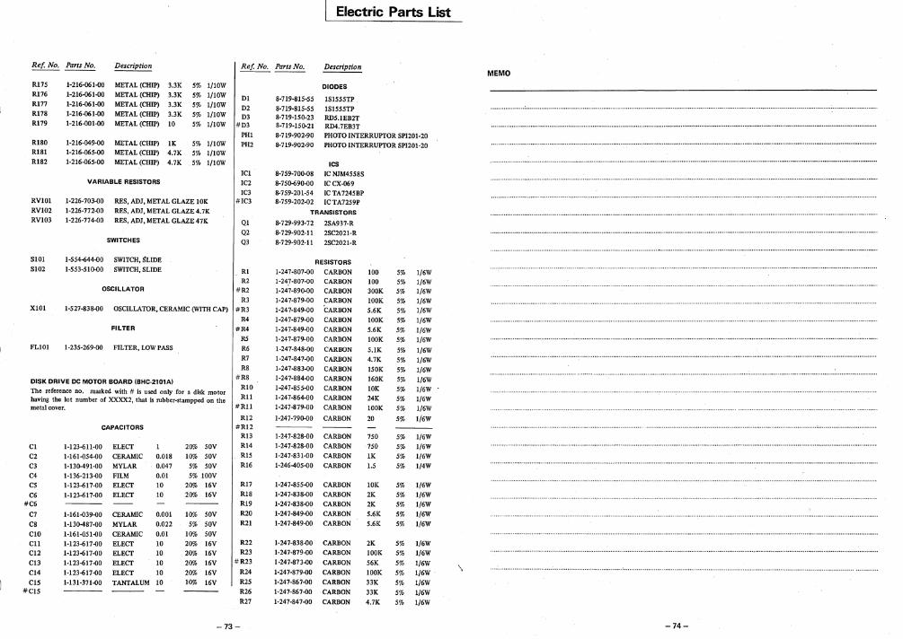
Ref. No. Parts No.
R175 RI76
RI77
R178
RI79
1-216·06J.OO
1-216-061.Q0 1-216.(J61.Q0
1-216.(J61.Q0
1-216·001.Q0
Description
METAL (CHIP) 3.3K
METAL (CHIP) 3.3K METAL (CHIP) 3.3K
METAL (CHIP) 3.3K
METAL (CHIP) 10
5% IjlOW
5% IjlOW
5% IjlOW 5% IjlOW
5% 1/l0W
DI
D2 D3
#D3
Electric Parts list
Description
DIODES
8-719·815-55 ISI555TP
8·719·815-55 ISI555TP 8-719-150-23 RD5.IEB2T 8-719-150-21 RD4.7EB3T
PHI 8-719-902-90 PHOTO INTERRUPTOR SP1201-20 RI80
RI81 RI82
RVIOI
RVI02 RVI03
SIOI
SI02
1-216·049.Q0 METAL (CHIP) lK 5% IjlOW 1-216-065.Q0 METAL (CHIP) 4.7K 5% I/iOW
1-216.Q65·00 METAL (CHIP) 4.7K .5% IjlOW
VARIABLE RESISTORS
1-226-703.Q0
1-226-772.Q0
1-226-774·00
RES, ADJ, METAL GLAZE 10K
RES, ADJ, METAL GLAZE 4.7K
RES, ADJ, METAL GLAZE 47K
SWITCHES
1-554-644.Q0 SWITCH, SLIDE
1-553-510-00 SWITCH, SLIDE
OSCILLATOR
PH2
ICI
IC2
IC3 #IC3
QI
Q2 Q3
Rl R2
#R2
R3 XIOI 1·527-838-00 OSCILLATOR, CERAMIC (WITH CAP) #R3
FILTER
PLIOI 1-235-269-00 FILTER, LOW PASS
DISK DRIVE DC MOTOR BOARD IBHC-2101AI
The reference no. marked with # is used only for a disk motor having the lot number of XXXX2, that is rubber-starnpped on the metal cover.
CI
C2
C3
C4 C5
C6 #C6
C7
C8
CIO
C11 CI2
CI3
CI4
CIS #C15
CAPACITORS
l-12H11-00 ELECT 20% 50V
1-161.Q54-00 CERAMIC 0.Q18 10% 50V
1-130-491-00 MYLAR 0.047 5% 50V 1-136-213.Q0 FILM 0.01 5% 100V 1-123-617.Q0 ELECT 10 20% 16V
1-123-617·00 ELECT 10 20% 16V
1-161.Q39.Q0 CERAMIC 0.001 10% 50V
1-130-487·00 MYLAR 0.022 5% 50V
1-161-051.Q0 CERAMIC 0.01
1-123-617.Q0 ELECT 10 1-123-617-00 ELECT 10 1-123-617.Q0
1-123-617.Q0
1-131-371.Q0
ELECT 10
ELECT 10
TANTALUM 10
10% 50V
20% 16V 20% 16V
20% 16V
20% 16V 10% 16V
R4 #R4
R5
R6
R7
R8 #R8
RIO
R11 #R11
RI2 #R12
R13 RI4
R15
R16
RI7
RI8 R19
R20 R21
R22 R23
#R23
R24
R25
R26
R27
-73-
8-719-902-90 PHOTO INTERRUPTOR SPI20l-20
ICS
8-759-700-08 IC NJM4558S
8-750-690.Q0 IC CX-069 8-759-201-54 8-759-202·02
[CTA7245BP [CTA7259P
TRANSISTORS
8-729-993-72 2SA937-R
8-729-902-11 2SC2021-R
8-729-902-11 2SC2021-R
RESISTORS
1-247-807-00 CARBON 1-247-807-00 CARBON 1-247-890-00 CARBON 1-247-879-00 CARBON
1-247-849.Q0 CARBON 1-247-879.Q0
1-247-849.Q0
1-247-879-00
1-247'848·00 1-247-847-00
1-247-883.Q0 1-247-884.Q0
1-i!47 -85 5-00 1-247-864-00
1-247-879-00
1-247-790-00
CARBON
CARBON
CARBON
CARBON
CARBON
CARBON
CARBON
CARBON CARBON
CARBON
CARBON
1-247-828-00 CARBON 1-247-828-00 CARBON
1-247-831-00 CARBON
1-246-405.Q0 CARBON
1-247-855.Q0 CARBON
1-247-838.Q0 CARBON
1-247-838.Q0 CARBON 1-247-849.Q0 CARBON
1-247-849-00 CARBON
1-247-838-00 CARBON 1-247-879-00 CARBON
1-247-873.Q0 CARBON
1-247-879.Q0 CARBON
1-247-867.Q0 CARBON
1-247-867.Q0 CARBON
1-247-847.Q0 CARBON
100 5% Ij6W 100 5% 1/6W 300K 5% Ij6W
lOOK 5% 1/6W 5.6K 5% 1/6W
lOOK
5.6K
lOOK
5.IK 4.7K
150K 160K
10K
24K
lOOK
20
750
750
IK
1.5
10K
2K
2K
5.6K
5.6K
5%
5%
5%
5%
5%
5% 5%
5%
5% 5%
5%
1/6W
1/6W 1/6W
1/6W 1/6W
1/6W
1/6W 1/6W
1/6W 1/6W
1/6W
5% 1/6W
5% 1/6W 5% Ij6W
5% Ij4W
5% 1/6W
5% 1/6W 5% 1/6W
5% Ij6W
5% Ij6W
2K 5% Ij6W
lOOK 5% 1/6W
56K
lOOK
33K
33K
4.7K
5%
5%
5%
5%
1/6W Ij6W
Ij6W
Ij6W
5% Ij6W
MEMO
\
-74-
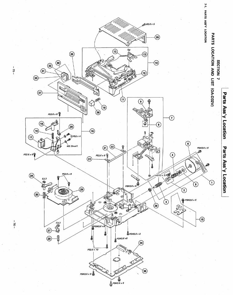
I .... '" I
I .... '" I
J»-, (j;PS2x 4 ,
~ ~ ~ 16
I 8
~c~
7
~ :ll
iii » z: -< ro n "tI ~ l> o JJ z -I en
5 (")
~ o en Z ~ l> ::! z 0 c Z r- .....
~ o l>
E N $
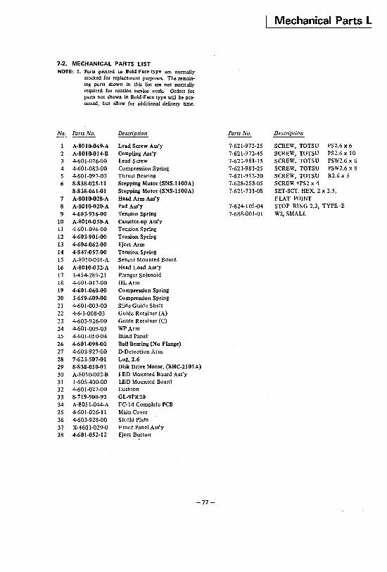
7-2_ MECHANICAL PARTS LIST NOTE: 1. Parts printed in Bold-Face type are nonnally
stocked for replacement purposes. The remain-ing parts shown in this list are not normally required for routine service work. Orders for parts not shown in Bold·Face type will be pro-cessed, but allow for additional delivery time.
No. Parts No. Description
A-8010-049-A Lead Screw Ass'y 2 A-8010-014-B Coupling Ass'y
4-601-076-00 Lead Screw 4 4-601-083-00 Compression Spring 5 4-601-097-00 Thrust Bearing 6 8-838-025-11 Stepping Motor (SNS-IIOOA)
8-838-061-01 Stepping Motor (SNS-1500A) 7 A-80I O-028-A Head Ann Ass'y 8 A-80 I O-020-A Pad Ass'y 9 4-603-936-00 Tension Spring
10 A-80 1 0-0 30-A Cassette-up Ass'y II 4-601-096-00 Tension Spring 12 4-603-901-00 Tension Spring 13 4-604-062-00 Eject Arm 14 4-847-057-00 Tension Spring 15 A-8050-001-A Sensor Mounted Board 16 A-8010-032-A Head Load Ass'y 17 1-454-289-21 Plunger Solenoid 18 4-601-017-00 HLArm 19 4-601-060-00 Compression Spring 20 3-659-609-00 Compression Spring 21 4-601-003-00 Slide Guide Shaft 22 4-6-1-008-03 Guide Retainer (A) 23 4-603-926-00 Guide Retainer (C) 24 4-601-009-03 WPArm 25 4-601-050-04 Blind Panel 26 4-601-098-00 Ball Bearing (No Flange) 27 4-603-927-00 D-Detection Arm 28 7-623-507-01 Lug, 2.6 29 8-838-050-01 Disk Drive Motor, (BHC-2101A) 30 A-8050-002-B LED Mounted Board Ass'y 31 1-605-400-00 LED Mounted Board 32 4-601-027-00 Cushion
33 8-719-900-92 GL-9PR20 34 A-8051-044-A FC-14 Complete PCB 35 4-601-026-11 Main Cover 36 4-603-928-00 Shield Plate 37 X-4601-029-0 Front Panel Ass'~ 38 4-601-052-12 Eject Button
-77-
Parts No.
7-621-972-25 7-621-972-45 7-621-981-15 7-621-981-25 7-621-912-20 7-628-253-05 7-621-731-08
7-624-105-04 7-688-001-01
Mechanical Parts L
Description
SCREW, TOTSU PS2.6 x 6 SCREW, TOTSU PS2.6 x 10 SCREW, TOTSU PSW2.6 x 6 SCREW, TOTSU PSW2.6 x 8 SCREW, TOTSU B2.6 x 5 SCREW +PS2 x 4 SET-SCf. HEX. 2 x 2.5, FLAT POINT STOP RING 2.3, TYPE-E W2, SMALL

MEMO
-78-
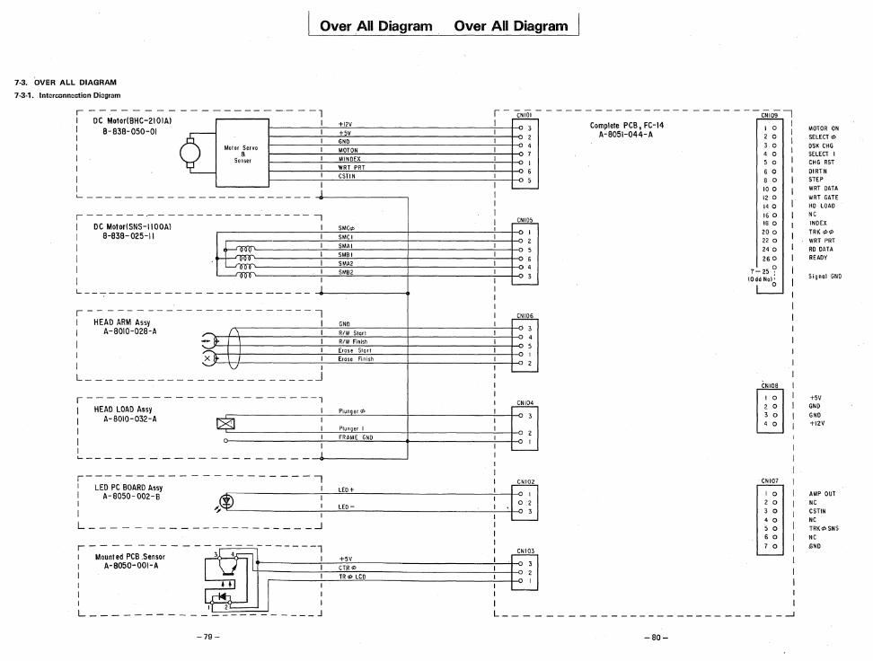
7-3. OVER ALL DIAGRAM
7-3-1. Intorconnoction Diagram
Over ,All Diagram Over All Diagram
r - - - - - - - - - - - - - - - - - -,- - -, r - CNiOi - - - - - - - - - - - - - - - - - - - - - - - CriIOS-' I DC MotorIBHC-210IAI 1-____ :-1 _.:!:+~12:!..V ____________ --;:--r-o Complete PCB, FC-14 I 0
I B-B3B-050-0I +5V A-B051-044-A 2 0
I GND 3,0 I Molor :"vo MOTON 4 0
I Sensor MINDEX L 5 0 I 1-____ +----2W!OR':!:T2P~R.!.T ____________ _;_-ro 6 6 0
CSTIN 8 0
I 100 I L____________ ~O
r-------------I DC MotorlSNS-11 OOAI I B-838- 025-11
I I I I L ____________ _
r------------I HEAD ARM Assy I A-8010-028-A
-----------------------,
I I
~ I I
, -'.!Y I I L.......rffl"\ I 1 -----------
-----------, I I
I I I
-~ I ;::::: I X~ I - V I
L ___________ _
r-----------I HEAD LOAD Assy I A-BOIO-032-A
I I I L- __________ _
___________ J
- - - - - - - - --1
I
~ I I I
I 1 --- - - ----
r----------------------,
~ SMC¢ ,I
SMCI I 2
SMAI I 5
5MBI I 6
SMA2 I 4
5MB2 3
'---
,..Qill!§.. GND
3 R/W Sian
4 R/W Finish
5 Erose Stort
I Erase Finish
2 '---
~ Plunger(/> 3
Plunger I 2
FRAME GND I
'---
CNI02 LED+ .[] I LED PC BOARD Assy ~-------_i_I-----"'!"---'--------------___;-
I A-B050-002-B ~ I LED-I ~~~~------~-~~----------~___;~ I
L ____________________ ...1
CNI03 +5V
r--------I Mount ed PCB .Sensor I A-B050-001-A CTR¢
1 TR ¢ LCD
140
160 180
200
22 0
240
260
7-259 10dd Nol:
o
CNI08
[ill 2 0
3 0
4 0
'CN107
10
2 0
3 0
4 0
5 0 6 0
7 0
-------------------------~
-79- -80-
MOTOR ON
SELECT ¢
DSK CHG SELECT I CHG RST
DIRTN STEP
WRT llATA
WRT GATE HD LOAD NC
INOEX
TRK ¢¢
WRT PRT RD DATA
READY
Signal GNO
+5V GND
GND +12V
AMP OUT
NC
CSTIN
NC TRK¢ SNS
NC
.GND
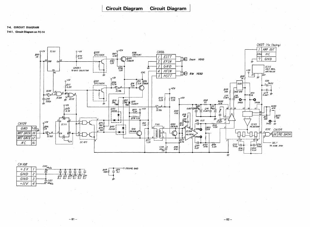
7-4. CIRCUIT DIAGRAM
7-4·1. Circuit Diagram on FC·14
'fV [CIOI
CNI09
&ND
fII07 IX
WR1GATE IZ NC 16
CNI08
+SV 1 GND Z GND 3 +/2/1 4
ZJ IRQ
Rz 46
'SV
!U74 J.JX
CPUERT ro OIlZ COLLECTOR
'SV
fIlii l.ll<
-81-
1(107
RI7I 10K 8173 10K
Circuit Diagram
/2103 i-ISSI2.3 I
Rlf8 lZO{//zW)
0107 lS86Z4
1_ 0.1 '"' qr"'"' ~
Circuit Diagram
CNIOb E5T1
Z EFIN X Erose HEAD
3 G-ND 4 HFIN 5 HSTT
- /?/w HEAl>
+Itv
RI7S R176 +ltV 1?2X l.lK
RI48 117O
-82-
CNID? (For Checkl'9J
.----\ I AN? OUT
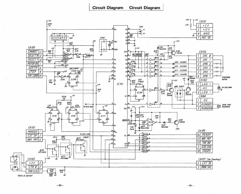
Circuit Diagram Circuit Diagram I
'SV
/j14S If(
~----------------------'9R'l
rtHtH-J'il slot I I I I ~-- ---- ----' 8,110
'OX
+J'I
ePIOI
CNI09 .Sf
CHGRST J~~ SELECTe 2 ~ SELECT! 4
II ~!JJ IPJI
9: '5 ;-;101.
1I117 4.7K
J3J'o...J2
Icm
8.1J8 l.21
~ z=
rf-'~YbJI I ~'JL. i .!5"" : I EXta/ L _~
5 R,
'I II I1OTORON I DIRTN 6 STEP 8
HDLDAD 14-
~A~8/OJ 1 '''-~''K
rl~ 8AI6 tSf~-m IK~B oiL
ClOI J: 1(/OS 1009
7oo<r fA Zi 'Z tSV
T /!/04 IX L-----------------+----+4
RVIOI 'Sf
'0; 1l'46 /!ISO
CllJ + I K lSI! ,,14 SEll-77JDIZ4P1N a4Zf~ t IS ~02Z
,.......m. 8 0 ~ U B of""J'--t----, i..ll. 0 O!L....tti.RI4
ICIlI
CNIOI I1IilDEX I -CST IN S WRT PRT 6
/cliO ](110
,--~-+--"II'-lC,K ~ {L
~ Rs
~--~-----r~----~Z~6~m
tSf
fIl81 4.7K
III8I 4.7K
r----~1 r---- , I ....
I I : I I I I I I I I I L ____ ..J
--' ~"J
J1J KKJ'.niI1 I J •
.llY ~ .SV CNIOI
LlOI 2 +5 V - 3 +/2 V
,J;: 4 GND 7 MOT ON
13A 5102 OJ A
Rl47 .dl B 818J l·~ X,
S e mv ~ I
MY ,~::~ :~~, Vccl"r, __ ~-",_--, III79 ~QIOS CNIOJ Rt ~ frk~!1: ~~ ____ ~.2 ,~r. IIISIt:.(~2~S8~7J:4-1--11/l~S~M~CJ9Cl---1 0- 40 I '" r*' I,. '1 : JJX , ~ '2 SI1C! -".Ju...~ 41 v .r*" I/J " In..:: 3 5MB 2 --'OT'--<
Pl.p, ~;S! ~ l,z WIlT /SZJ4IJH 4 h! " ~ I, Dill IS1J48H 5
2';~~ ~I " .r*" :m Dill ISZJ48H p,jf'9Y~;"""---*-"+--C v.O+-+-i',"'-----j4I-'----+n~iO<7,-8H--l 6
,s~ DISZ CIZS I 's.: eN 102 ~ZK +4."'Izr I t/ZY L 8f~g
DIO'I IS1J4IJH
, ,1" SI1A 2 SMA !
511 B I -'Or'-- STEPPIN6 HOTOR
.T " I. I ff~ I LED + 3>. I~ .w., : f2IOS 151837 I-?-+,_N-'--C'------i • .!H lISE lAHP f-.--z 8Q~W-:v ,l""" 116 r---l ,_
ICl09 : 1~JZ ~/:: if t gill r- 3 L ED -0, ~l-4 A Q~ : 2586& L _ J 250m CHI04
I r-~-----.
~ I / NC o.liJ '" 'r*" ;'4 2 PLUNGER/I/<:::, HEAD lJJAD
VSsriJ"V tllV LV..J ~----+---i..:3~PL!(j,~WI~I:S:~t.:?!l(~tZ'~ SOlENOID
, f~ ~:~~ I 1::: 8163 ~, RES~ IZ~,,!.~ ~/80 ~>'.3_~...,M_~Jow~a-.ff ~:14
E11A81~ + I! Z + 0';;
ClZ6 '. f/!:JH8Z HD9.11f81 ~~ U~
CN/09 ~
RI l4s ~. 26 READV .---If--~~~~l~·--6---:-----------------___j . .22 WRT PI?T
Ro ~4 ~11 20 7l?X tZ'¢ R?r----t-t~~z~~;a;1I~·3----------------------I3 DSJ( OIG
'0 (J 18 INDEX
eN/03 OTCIf4EK Cil/07 (FiJrChecklf1!J)
TSV 3 ~--~----------------------------------------~3 CSTIiI
tiCiT.~R~¢~2d-~~~~~~----------~------JL----------------------------------------~~ mx~SNS TRBCLD I ~ ~f~
TRACK, 5l!HSER ~ I J.
-83- -84-
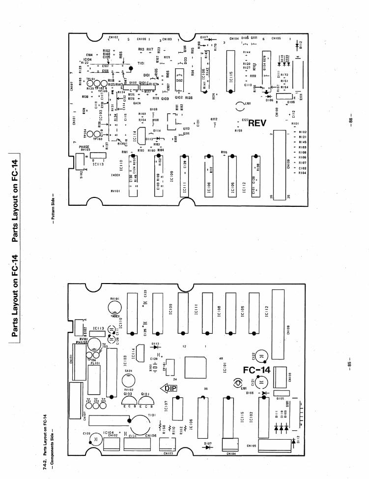
'lit or-
I
U LL C 0 .... j
~ CO
..J
~ CO 0..
'lit or-
I
U LL C 0
~ 0 > CO
..J
a "-co
0..
... ;:; II. C o
'" " en E " t: ~ I
.. .. ::J "'C o ._ > en !I tl w .. 1:: c ~ 8.
E ~ <3 ;t I
CNI02 , I CNIOS I 3 CNIOS Ol~
o z u
RII3 RII7 RI62 + Ln
RI48 '+ !!! Cl04 '+ elOS 0:: I
ICI04 i' t TIOI 'R122 CI07 + + ~ !l!:g ~ I + C10S =-~ =t 0101 ~ .... a: a: +'~~--t r-'-I ..... .
6 R171 d ........
" T(j°O'O' RIIB + i 0103 ~RI6]7. + e '" + RI25RI4Dr----1L._ !,,! ",' 02 t + EL- C -B1 EiiiiT"B I-'-
RI:' TP~';!j05 f E'2~ RI75 + + RI;B QIDS
'" o
t-'-d
8 ,.....,0
B 1:1
0>
'"
:~ ~~~;.~ co -~
U
-+
~
;;+ .. + - .., R176 + R130 '+ U t : GAIN
~t= c;; = 0108 U fr)f.J i%:+-E-u RIG3"[
QID2 RIZ6
" "
o
" u
r-
r.I+ 0 .. , ~ + I = - t M = ft16~ D1D8 !:! a: u '+} ~--+ + +I
1'"""'1. t
O Ii-'-~ ....... 0114 L..... ..... D113~
'+ R1BJ
~ 0> l I ~oa~+ +I + .... TPI03 ---.J, ~
:;; ~13SU +~
QIIl I-'-Q114
R161 ... R180 R ;60 Rrn4 + ;;; PHASE
RYI03
o I + ~. Dmc:::J ~< IC1I3 ;:! .
I;:; INDEX
'"
RVIDI
RVIOI o lNOEX
o D; ICI13 (;::~~~
0'"
+ +,
m N
U
;:::
~ N
U
0113 -..-
<n o
<n o
;:!
0> N
U
;:!
12
+ ~ u
QI12
t ~
'" o
;:!
T
:: c:::J '~\o " .. g-~/" oUTPI04 'n
"' gO o - C 12,;1 1 +-0
..L. 0
0= iLL - u x, 24 D
O RVI02 0 U W QI03 QIOI r-
TP ~ ~ !iU T02 105 0. E C,' B ;:!
uOO nOI <0
II V\ t~ f~ ~f ~ ICID4 + J( Cw',06 [J C109~ CNI02 II
00 b:=d CNI03
36
'" o
8105
4B
CNID4 OIO~ Qt1l
I....... I-'-
CNI05
f~
'" o
RI44
RI20 ~4 R~21 ~
... R119
t
I-'-
el13 ~+ t
;;: '-.Ir ...... 0106
~LlOI
'-.J
+ CI27REV RI59
'" o
" +~
" ~+
i~+ ,u
;:!
~f-'\ u\::.J
W N
!~!~! = RI72 o +
RISI +
r;; RIS.
Ch-~ " o
i'i
0105
N
+ = U
0>
RIOI
... RI02
... RI21
... RUS
.... RIOS
... RICB
... RIOS
o ... RI07
" U ... CI02
on N
0> o
" U
... RI04
FC-14[] ~ ~0 ~ ~101 \...-.J
0106 - ~ c:::J 0105
~ ~ ~ I I:: ~g Cl oc
*** ~ CN105/ It ~
=
CD ex> I
Il) ex> I
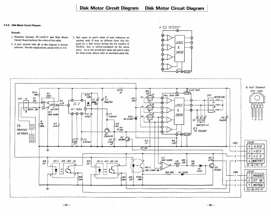
7-4-3. Disk Motor Circuit Diagram
Remark:
1. Numbers between FC-14/FC-9 and Disk Motor Circuit Board indicate the color of the cable.
2. A part marked with !;iii in the diagram is factory selected. For the replacement, please refer to 5-8.
Disk Motor Circuit Diagram
3. Part name or part's value of part reference no marked with # may be differed from this diagram for a disk motor having the lot number of XXXX2, that is rubber-stampped on the metal cover. As to the actual part name and part's value for these parts, please refer to electrical parts list.
Disk Motor Circuit Diagram
# Ie3 TA7259P
r------------------------------------------------------------------------------------------,
#R3 lOOK R5
lOOK RI 100 CN/~ 1 ~ I ~ I 3.... R6 r--l,-O-+,-----"'IIV-1I4'1_,....... ..z... + Ji... S.I K
t.I -:r CI
I L;-JBi #RZ 100 4.... IJ/SOV leI NJIf-~SS6S
F~ P;NTCOIL ~ 60P/feES ~
# R4 R7 1001( 4.7K
#RI2 20
. ~iJ. " ~wJ, i~r.F ~ ,."",,, Rll HI H4 ~ - ~ ~o J ~_ I~ 6r---~~-o~c~J,O,O'-,
~~. LOGIC 7>--_-I-+-c>-t-:BJi">n<Q,O'0"'-1 >--Hl~ I
CI4 lOdjl6V
#D3 l'. HJ4 f D~ljlE 1 + + '-- A ,0'
RD-iIE8zr". ~ ~ O/~
~~ ~M I n RIO b>-J] 10AF/lhVA'J
1/ \J # Z411 TA-7Z45BP t--~--r~~QIY-~~~'v-~----r---~--r--r-r~~'~-+' ~
2SA'l37R Qi? fll C~,8r T, Cl o~~J O.047.Q.F
C(I'zT ZSCa:li'~ o"~l
I
RI,j IK
RI7 lOll
Rlh ua
RZ6
R27 4-71(';
ZK r---l i-----k, I' I 4- I--........ >--~'v-"""""""'~ ..... -t[ , '6 ' 'rS' \ - )PH-] + "
.131( .. I?' D~
r ~ 03 ,,_I: : 1-: : \ N7L-S/41E-A86
: '-:: : :-, I I , ___ / 4 RZ4 lOOK DI.!JtfSS IJISSJ ZSCZOZI
+
RI(I· j}H-, SPI-?O/-zo ~~'9~P~-!1 5P~~!~~-!~, I~ ~---?'~\ ~~~-4.f.l:88S o.~'/m: ~~~ L_~ --<D---;,'J...,---, , , I...._J IJ ...
C L ___________ J RlO ~ L ___________ ~ HZI RZZ #RlJ ~
, I
L-c 2
J
r- 4
f-
So6K '.f.6K ZK 111011 ~: ; I
" I I I I I L ______________________________________________________________________________________________ ~
-87- -88-
""$c Hall Element
HTS - l03A
I 2 J 4
icNIo,-----] I 4 GND i
I J +IZV I 2 +s V I
I I "6 WRTPIfT i LEf'..:/iU"i..:'?.._J r--------l I eN/OI I
I / I1INfJEX \ I
5 CST IN I 7 MOTON i
I FC-/4/FC-Q I . '--_________ J
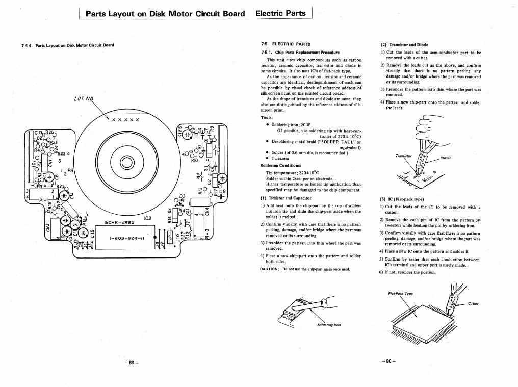
Parts Layout on Disk Motor Circuit Board
7-4-4. Parts Layout on Disk Motor Circuit Board
LOT. NO
xxxxx
-89-
Electric Parts
7·5. ELECTRIC PARTS
7·5·1. Chip Parts Replacoment Procedure
This unit uses chip componb.lts such as carbon resistor, ceramic capacitor, transistor and diode in some circuits. It also uses IC's of flat·pack type.
As the appearance of carbon resistor and ceramic capacitor are identical, destinguishrnent of each can be possible by visual check of reference address of silk-screen print on the printed circuit board.
As the shape of transistor and diode are same, they also arc distinguished by the reference address of silkscreen print.
Tools:
• Soldering iron; 20 W (If possible, use soldering tip with heat-con
troller of 270 ± 10°C) • Desoldering metal braid ("SOLDER TAUL" or
equivalent) • Solder (of 0.6 mm dia. is recommended.) • Tweezers
Soldering Conditions:
Tip temperature; 270± 10°C Solder within 28ec. per an electrode Higher temperature or longer tip application than specified may be damaged to the chip <;omponent.
(1) Resistor and Capacitor
1) Add heat onto the chip-part by the top of soldering iron tip and slide the chip-part aside when the solder is melted.
2) Confirm visually with care that there is no pattern peeling, damage, and/or bridge where the part was removed or its surrounding.
3) Prcsolder the pattern into thin where the part was removed.
4) Place a new chip-part onto the pattern and solder both sides.
CAUTION: Do not use the chip-part again once used.
(2) Transistor and Diode
1) Cut the leads of the semiconductor part to be removed with a cutter.
2) Remove the leads cut as the above, and confirm visually that there is no pattern peeling, any damage and/or bridge where the part was removed or its surrounding.
3) Presolder the pattern into thin where the part was removed.
4) Place a new chip-part onto the pattern and solder the leads.
Transistor
JI! -..../ I ~ .'fo
~ (3) IC (Flat-pack type)
1) Cut the leads of the IC to be removed with a cutter.
2) Remove the each pin of IC from the pattern by tweezers while heating the pin by soldering iron.
3) Confirm visually with care that there is no pattern peeling, damage, and/or bridge where the part was removed or its surrounding.
4) Place a new IC onto the pattern and solder it.
5) Confirm by tester that each conduction between IC's terminal and upper port is surely made.
6) If not, resolder the portion.
Cutter
-90-
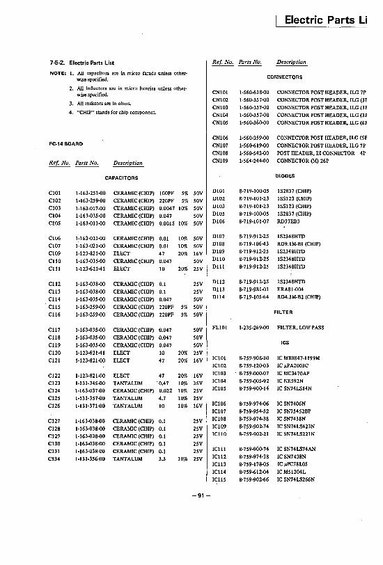
Electric Parts Li
7-5-2_ Electric Parts List Ref, No. Parts No. Description
NOTE: 1. All capacitors are In micro farads unless other-wise specified. CONNECTORS
2. All Inductors are In micro henries unless other-wise specified. CNI0l 1-560-618-00 CONNECTOR POST HEADER, lLG 7P
3. All resistors are In ohms. CNI02 1-560-357-00 CONNECTOR POST HEADER, ILG (31
4. "CHIP" stands for chip component. CNI03 1-560-357-00 CONNECTOR POST HEADER, ILG (31
CNI04 1-560-357-00 CONNECTOR POST HEADER, ILG (31
CNI05 1-560-360-00 CONNECTOR POST HEADER, ILG (61
CNI06 1-560-359-00 CONNECTOR POST HEADER, ILG (5F FC-14 BOARD CNI07 1-560-619-00 CONNECTOR POST HEADER, ILG 7P
CNl08 1-560-542-00 POST HEADER, EI CONNECTOR 4P
Ref, No. Parts No. Description CNI09 1-564-244-00 CONNECTOR (M) 26P
CAPACITORS DIODES
CI0l 1-163-251-00 CERAMIC (CHIP) 100PF 5% 50Y DI0l 8-719-100-05 IS2837 (CHIP)
CI02 1-163-259-00 CERAMIC (CHIP) 220PF 5% 50Y Dl02 8-719-101-23 ISS123 (CHIP)
CI03 1-163-017-00 CERAMIC (CHIP) 0.0047 10% 50Y Dl03 8-719-101-23 ISS123 (CHIP)
CI04 1-163-035-00 CERAMIC (CHIP) 0.047 50Y Dl05 8-719-100-05 IS2837 (CHIP)
CI05 1-163-011-00 CERAMIC (CHIP) 0.0015 10% 50Y DI06 8-719-101-07 RD33EB3
CI06 1-163-021-00 CERAMIC (CHIP) 0.01 10% 50Y D107 8-719-912-25 IS2348HTD
CI07 1-163-021-00 CERAMIC (CHIP) 0.01 10% 50Y DI08 8-719-10643 RD9.1M-Bl (CHIP)
CI09 1-123-821-00 ELECT 47 20% 16Y DI09 8-719-912-25 IS2348HTD
CliO 1-163-035-00 CERAMIC (CHIP) 0.047 50Y DllO 8-719-912-25 IS2348HTD
Clll 1-123~2141 ELECT 10 20% 25Y Dill 8-719-912-25 IS2348HTD
C1l2 1-163-038-00 CERAMIC (CHIP) 0.1 25Y D1l2 8-719-912-25 IS2348HTD
C1l3 1-163-038-00 CERAMIC (CHIP) 0.1 25Y DI13 8-719-981-01 ERA81-o04
C1l4 1-163-035-00 CERAMIC (CHIP) 0.047 50Y D1l4 8-719-105~4 RD4.3M-B2 (CHIP)
C1l5 1-163-259-00 CERAMIC (CHIP) 220PF 5% 50Y
C1l6 1-163-259-00 CERAMIC (CHIP) 220PF 5% 50Y FILTER
C1l7 1-163-035-00 CERAMIC (CHIP) 0.047 50Y FLI0l 1-235-269-00 FILTER, LOW PASS
C1l8 1-163-035-00 CERAMIC (CHIP) 0.047 50Y
C1l9 1-163-035-00 CERAMIC (CHIP) 0.047 50Y ICS
C120 1-12H2141 ELECT 10 20% 25Y
C121 1-123-821-00 ELECT 47 20% 16Y ICI01 8-759-908-30 IC MB8847-1199M
ICI02 8-759-120-03 IC Jd'A2003C
C122 1-123-821-00 ELECT 47 20% 16Y ICI03 . 8-759-000-07 ICMC3470AP
C123 1-131-345-00 TANTALUM ·0.47 10% 35Y ICI04 8-759-005-92 ICNE592N
C124 1-163-037-00 CERAMIC (CHIP) 0.022 10% 25Y ICI05 8-759-900-14 IC SN74LS14N
C125 1-131-357-00 TANTALUM 4.7 10% 25Y
C126 1-131-371-00 TANTALUM 10 10% 16Y ICI06 8-759-974-06 ICSN7406N
ICI07 8-759-954-52 IC SN75452BP
C127 1-163-038-00 CERAMIC (CHIP) 0.1 25Y ICI08 8-759-974-38 IC SN7438N
C128 1-163-038-00 CERAMIC (CHIP) 0.1 25Y ICI09 8-759-902-74 IC SN74LS423N
C129 1-163-038-00 CERAMIC (CHIP) 0.1 25Y ICllO 8-759-902-21 IC SN74LS221N
C130 1-163-038-00 CERAMIC (CHIP) 0.1 25Y
C131 1-163-038-00 CERAMIC (CHIP) 0.1 25Y ICl11 8-759-900-74 IC SN74LS74AN
C134 1-131-356-:00 TANTALUM 3.3 10% 25Y IC1l2 8-759-974-38 ICSN7438N
IC1l3 8-759-178-05 IC pPC78L05
IC1l4 8-759~12.Q4 IC M51204L
IC1l5 8-759-902~6 IC SN74LS266N
-91-
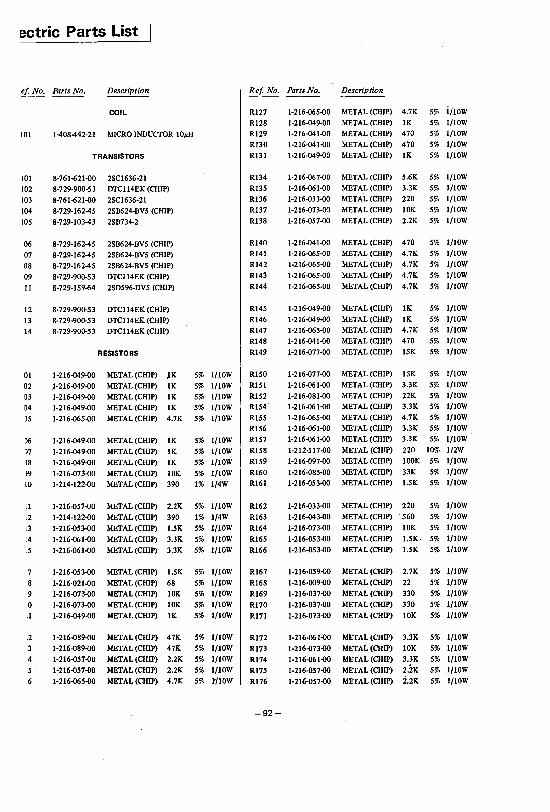
ectric Parts List
ef. No. Parts No. Description
lOl
lOl 102
103
104 105
.06 07 08 09 11
12 13 14
01 02 03 04
05
)6
)7
)8
)9
10
11 12
13 ~4
.5
:0 :1
4
5
COil
1408442-21 MICRO INDUCTOR lO~H
TRANSISTORS
8-761-621-00 2SC1636-21 8-729-900-53 DTC114EK (CHIP)
8-761-621-00 2SC1636-21 8-729-16245 2SB624-BV5 (CHIP) 8-729-10343 2SB734-2
8-729-16245 2SB624-BV5 (CHIP) 8-729-16245 2SB624-BV5 (CHIP) 8-729-16245 2SB624-BV5 (CHIP) 8-729-900-53 DTC114EK (CHIP) 8-729-159-64 2SD596-DV5 (CHIP)
8-729-900-53 DTC114EK (CHIP) 8-729-900-53 DTC1l4EK (CHIP) 8-729-900-53 DTC114EK (CHIP)
1-216-049-00 1-216-049-00 1-216-049-00 1-216-049-00 1-216-065-00
1-216-049-00 1-216-049-00 1-216-049-00 1-216-073-00 1-214-122-00
RESISTORS
METAL (CHIP) ,lK METAL (CHIP) lK METAL (CHIP) lK METAL (CHIP) lK METAL (CHIP) 4.7K
METAL (CHIP) lK METAL (CHIP) lK METAL (CHIP) lK METAL (CHIP) 10K METAL (CHIP) 390
1-216-057-00 METAL (CHIP) 2.2K 1-214-122-00 METAL (CHIP) 390 1-216~53-o0 METAL (CHIP) 1.5K 1-216-061-00 METAL (CHIP) 3.3K 1-216-061-00 METAL (CHIP) 3.3K
1-216-053-00 1-216-021..QO 1-216-073-00 1-216-073-00 1-216-049-00
1-216-089-00 1-216-o89~0
1-216-o57~0
1-216-057-00 1-216-065-00
METAL (CHIP) 1.5K METAL (CHIP) 68 METAL (CHIP) 10K METAL (CHIP) 10K METAL (CHIP) 1K
METAL (CHIP) 47K METAL (CHIP) 47K METAL (CHIP) 2.2K METAL (CHIP) 2.2K METAL (CHIP) 4.7K
5% 1/10W 5% 1/10W 5% 1/10W 5% 1/10W 5% 1/10W
5% 1/10W 5% 1/10W 5% 1/10W 5% 1/10W 1% 1/4W
5% 1/10W 1% 1/4W 5% 1/10W 5% 1/10W 5% 1/l0W
5% 1/10W
5% 1/10W 5% 1/l0W 5% 1/10W 5% 1/10W
5% 1/10W 5% 1/10W 5% 1/10W 5% 1/10W 5% l'/lOW
Ref. No. Parts No. Description
R127 R128 R129 Rl30 Rl31
R134
R135 R136 R137 R138
R140 R141 R142 R143 R144
R145 R146 R147 R148 R149
R150 R151 R152 R1S4
RlSS RlS6 RlS7 RlS8 R159 R160 R161
R162 R163 R164 R165 R166
R167 R168 R169 R170 Rl71
R172 R173 R174 R17S R176
-92-
1-216-065-00 METAL (CHIP) 4.7K 1-216-049-00 METAL (CHIP) lK 1-216-041-00 METAL (CHIP) 470 1-216-04l.Q0 METAL (CHIP) 470 1-216-049-00 METAL (CHIP) 1K
1-216-067-00 1-216-061-00 1-216-033-00 1-216-073-00 1-216-057-00
1-216-041-00 1-216-065-00 1-216-065-00 1-216-065-00 1-216-065-00
1-216-049-00 1-216-049-00 1-216-065-00 1-216-041-00 1-216-077-00
1-216-o7HO 1-216-061-00 1-216-081-00 1-216-061.Q0
1-216-06S-00 1-216-061.Q0
1-216-061-00 1-212-S 17-00
1-216-097-00 1-216-o8S-00 1-216-053-00
METAL (CHIP) S.6K METAL (CHIP) 3.3K METAL (CHIP) 220 METAL (CHIP) 10K METAL (CHIP) 2.2K
METAL (CHIP) 470 METAL (CHIP) 4.7K METAL (CHIP) 4.7K METAL (CHIP) 4.7K METAL (CHIP) 4.7K
METAL (CHIP) 1K METAL (CHIP) 1K METAL (CHIP) 4.7K METAL (CHIP) 470 METAL (CHIP) lSK
METAL (CHIP) lSK METAL (CHIP) 3.3K METAL (CHIP) .22K METAL (CHIP) 3.3K METAL (CHIP) 4.7K METAL (CHIP) 3.3K METAL (CHIP) 3.3K
METAL (CHIP) 220 METAL (CHIP) lOOK METAL (CHIP) 33K METAL (CHIP) 1.5K
5% i/low S% 1/10W S% 1/10W S% 1/10W S% 1/l0W
S% 1/10W 5% 1/10W 5% 1/10W S% 1/10W S% 1/10W
S% 1/10W S% 1/10W 5% 1/10W S% 1/10W 5% 1/10W
5% 1/l0W S% 1/l0W S% 1/10W S% 1/10W S% 1/10W
S% l/10W 5% l/10W 5% 1/10W S% 1/10W S% 1/10W 5% 1/10W S% 1/10W
10% 1/2W S% 1/10W S% 1/10W 5% 1/10W
1-216-033-00 1-216-043-00 1-216-073-00 1-216-053-00 1-216-053-00
METAL (CHIP) 220 5% 1/10W METAL (CHIP) 560 S% 1/10W METAL (CHIP) 10K S% 1/l0W METAL (CHIP) UK - S% 1/10W METAL (CHIP) UK S% 1/10W
1-216-059-00 1-216-009-00 1-216-03HO 1-216-037-00 1-216-073-00
METAL (CHIP) 2.7K
METAL (CHIP) 22 METAL (CHIP) 330 METAL (CHIP) 330
METAL (CHIP) 10K
1-216-061-00 METAL (CHIP) 3.3K 1-216-073-00 METAL (CHIP) 10K 1-216-061-00 METAL (CHIP) 3.3K 1-216-057-00 METAL (CHIP) 2.2K 1-216-057-00 METAL (CHIP) 2.2K
S% 1/10W 5% 1/10W 5% 1/10W 5% 1/l0W 5% 1/10W
5% 1/10W 5% 1/10W 5% 1/10W S% 1/10W S% 1/10W
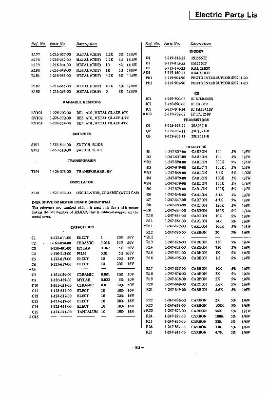
Ref. No. Parts No.
Rl77
R178
R179
R180
R181
R182
R183
1-216.Q57.Q0
1-216.Q57.Q0
1-216-001.Q0
1-216.Q49.Q0
1-216.Q65.Q0
1-216.Q65.Q0
1-216·295'()0
Description
METAL (CHIP) 2.2K
METAL (CHIP) 2.2K
METAL (CHIP) 10
METAL (CHIP) 1K
METAL (CHIP) 4.7K
METAL (CHIP) 4.7K
METAL (CHIP) 0
VARIABLE RESITORS
5% 1/10W
5% 1/10W
5% 1/10W
5% 1/10W 5% . 'lOW
5% 1/10W
5% 1/l0W
RV101 1-226·703-00 RE:', ADJ, METAL GLAZE 10K
RVI02 1-226·772.Q0 RES,ADJ,METALGLAZE4.7K
RVI03 1-226-774.Q0 RES, ADJ, METAL GLAZE 47K
SWITCHES
S191 1-554-644.()0 SWITCH, SLIDE
S102 1-553·510.Q0 SWITCH, SLIDE
TRANSFORMER
TI01 1426·073.Q0 TRANSFORMER, RF
OSCILLATOR
X101 1-527-838.Q0 OSCILLATOR, CERAMIC (WITH CAP)
DISK DRIVE DC MOTOR BOARD CBHC·2101AI
The reference no. marked with # is used only for a disk motor having the lot number of XXXX2, that is rubber-stampped on the metal cover.
C1
C2
C3
C4 CS
C6 #C6
C7 C8
C10
Cll C12
C13 C14
C15 #C15
CAPACITORS
1-123-611.Q0 ELECT 20% 50V
1-161.Q54.()0 CERAMIC 0.018 10% 50V
1-130-491.Q0 MYLAR 0.047 5% 50V
1-136-213.QO FILM 0.01 5% 100V
1-123-617.QO ELECT 10 20% 16V
1-123-617.Q0 ELECT 10 20% 16V
1-161.Q39.QO
1-130-487-00
1-161.Q51.Q0
1-123-617-00
1-123-617.Q0
1-123-617-00 1-123-617 .()O
1-131-371.Q0
CERAMIC 0.001
MYLAR 0.022
CERAMIC 0.01
ELECT 10
ELECT 10
ELECT 10 ELECT 10
TANfALUM 10
10% 50V
5% 50V
10% 50V
20% 16V
20% 16V
20% 16V
20% 16V
10% 16V
Electric Parts LiS"
Ref. No. Parts No. Des.;:ription
01 02 03
#03
PHI
PH2
IC1
IC2
IC3 #IC3
Q1
Q2 Q3
R1
R2
#R2
R3
#R3
R4
#R4
R5
R6
R7
R8 #R8
RIO
R11
#R11
R12 #R12
R13
R14
R15
R16
R17
R18
R19
R20
R21
R22
R23 #R23
R24
R25
R26
R27
DIODES
8-719-815-55 IS1555TP
8-719-815-55 IS1555TP 8-719-150-23 RD5.1EB2T 8-719-150-21 RD4.7EB3T 8-719-902-90 PHOTO INTERRUPTOR SPI201-20
8-719-902-90 PHOTO INTERRUPTOR SPI201-20
8-759-70O.Q8
8-750-690,()0
ICS
IC NJM4558S ICCX.Q69
8-7S9-201-54 IC TA7245BP 8-7S9-202.Q2 IC TA72S9P
TRANSISTORS
8-729-993-72 2SA937-R
8-729-902-11 2SC2021-R
8-729-902-11 2SC2021-R
RESISTORS 1-247-807.Q0 CARBON
1-247-807.Q0 CARBON
1-247-89O.Q0 CARBON
1-247-879'()0 CARB(,~1
1-247-849.Q0 CARBON
1-247-879.Q0 CARBON
1-247-879-00 CARBON
1-247-879.Q0 CARBON
1-247-848.Q0 CARBON
1-247-847.Q0 CARBON
1-247-883'()0 CARBON
1-247-884'()0 CARBON
1~47-8SS.Q0 CARBON
1-247-864.Q0 CARBON
1-247-879.Q0 CARBON
1-247-79O.Q0 CARBON
1-247-828.Q0 CARBON
1-247-828.Q0 CARBON
1-247-831.Q0 CARBON
1-246405.Q0 CARBON
1-247-8S5.Q0
1-247-838.Q0
1-247-838.Q0
1-247-849.Q0
1-247-849.Q0
1-247-838.Q0
1-247-879-00
1-247-873.Q0
1-247-879.Q0
1-247-867.Q0
1-247-867-00
1-247-847-00
CARBON
CARBON
CARBON
CARBON
CARBON
CARBON CARBON
CARBON
CARBON
CARBON
CARBON
CARBON
100
100 300K
lOOK
S.6K
lOOK
lOOK
lOOK
S.lK
4.7K
lS0K
160K
10K
24K
lOOK
20
750
750
1K
1.5
10K
2K
2K
5.6K
5.6K
2K
lOOK
56K
lOOK
33K
33K
4.7K
5%
S%
5%
S%
S%
S%
S%
S%
5%
S%
S%
5%
S%
S% S%
1/6W
1/6W 1/6W
1/6W
1/6W
1/6W
1/6W
1/6W
1/6W
1/6W
1/6W 1/6W
1/6W 1}6W
1/6W
S% 1/6W
S% 1/6W
S% 1/6W
S% 1/6W
S% 1/4W
5% S%
S%
S%
S%
S%
5%
S%
S%
S%
S%
S%
1/6W
1/6W
1/6W
1/6W
1/6W
1/6W 1/6W
1/6W
1/6W
1/6W
1/6W
1/6W
-93-
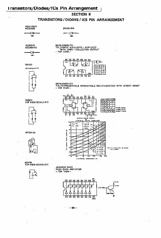
I ranslstors/Djodes/I Cs Pin Arrangement SECTION 8
TRANSISTORS I DIODES IICS PIN ARRANGEMENT
RD5.1EB2T RD33EB3
1S1555TP 1S2348HTD
1SS123
"" VIEW (SCALE ""1
1S2837 TOP VI EW (SCALE 4/1)
SP1201·20
RD77M TOP VI EW (SCA LE 4/1)
@,
ERA81·004
SN74LS266N (Til TTL 2·INPUT EXCLUSIVE - NOR GATE
WITH OPEN - COLLECTOR OUTPUT -TOP VJEW-
SN74LS423N (Til TTL RETRIGGERABLE MONOSTABLE MULTIVIBRATOR WITH DIRECT RESET -TOP VIEW-
PPA2003C (NEC) HIGH GAIN AMPLIFIER -TOP VIEW-
-94-
SK
INPUTS OUTPUTS Ro ABO 0 o x x 0 1 X 1 X 0 1
X X 0 0 1 O:LOW LEVEL 1 0 I 11. 1 :HIGH LEVEL 1 I 1 /L V X:OON'T CARE
FOlt ::! :::: .. Oft C • ,ooo~ I
~ ..
.
.
OUT
I.
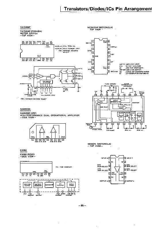
Transistors/Diodes/I Cs Pin Arrangemen1
TA7245BP
TA7245BP (TOSHIBA) MOTOR DRIVER -TOP VIEW-
FRS; FORWARD REVERSE SELECT
NJM4558S ......... NJM4558S (JRC)
La,Lb,Lc ; COIL TERMINAL
Ha,Hb,Hc ; HALL ELEMENT INPUT
FRS; FORWARD REVERSE SELECT
HIGH PERFORMANCE DUAL OPERATIONAL AMPLIFIER -SIDE VIEW-
B+IN 8-'N BOUT
CX069 ...... CX069 (SONY)
, -SIDE VIEW-
TC; TIME CONSTANT
r-----------------------~ I - I I
I I I I I I
IN"'" TIM' T • .- TIME OUT"'" TIIIIlCiNOYcc CO,!STANT CONST ..... T CONSTANT COtIST ..... T
-95-
MC3470AP (MOTOROLA) -TOP VIEW-
NE592N (MOTOROLA) - TOP- VIEW-
INPUT 2 I
~!~N SELECT 3
~~~N SELECT 4
OUTPUT 2 7
AMP IN :AMPUFIER INPUTS OFD ;OFFSET CECOUPUNG OC ;ONE-SHOT aNPONENTS AMP Cl.IT;AMPUFIER. OUTP1.ITS ADI ; ACTIVE OIFFERENTIAroR INPUTS OF ;DIFFERENTIATOR COMPONENTS
t2 ~tN SELECT
It g],.~N SELECT
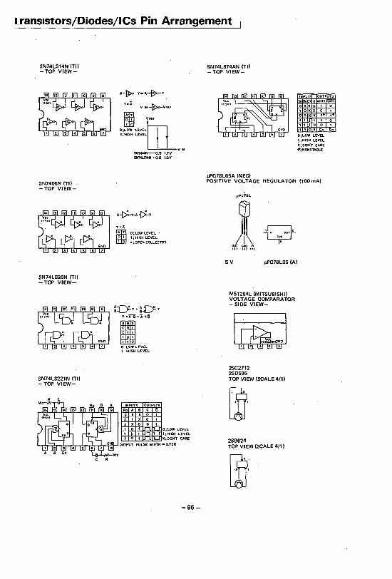
I.rans.stors/Diodes/. Cs Pin Arrangement
SN74LS14N (TI) -TOP VIEW.-
SN7406N (TI) -TOP VIEW-
SN74LS26N (Til -TOP VIEW-
SN74LS221N (Til -TOP VIEW-
Y-A VIN~"OJT
; I ;HIGH LEVEL O;L~: LEVELVDl
OUT
v IN SN7414N----O.9 I.TV SN7IILSI4N--o.B 1.6V
y. A
I v O;LOW LEVEL' 0, 1- HIGH LEVEL .
1 0 * ~ OPEN COLLECTOR
:Vy·:D-y· y.A='Bal+i
, , 0
O:LOW LEVEL I: HIGH LEVEL
INPUTS OUTPUTS R. A B Q a o x x 0 , X I X 0 I X X 0 0 1
I 0 I 1..J O;LOW LEVEL 1 .lL 1..J ,; HIGH LEVEL
o 1.lL X;DON'T CARE
-96-
SN74LS74AN (Til -TOP VIEW-
~C78L05A (NEC)
INPUTS OUTPUTS D On+I~
o 1 X X 1 0 lOX X 0 1 o 0 x x t* t *
1 1 0 1 1 0 0 1 1 t 0 X On On
O;lOW LEVEL I ; HIGH LEVEL X;DON'r CARE 1*;NONSTABLE
POSITIVE VOLTAGE REGULATOR (100 rnA)
pPCT8L
5V
~'NOtJT2 ON. . ~C78L05 (A)
M51204L (MITSUBISHII VOLTAGE COMPARATOR - SIDE VIEW-
2SC2712 2S0596 TOP VI EW (SCALE 4/1)
~ QJ' 2SB624 TOP VIEW (SCALE 4/1)
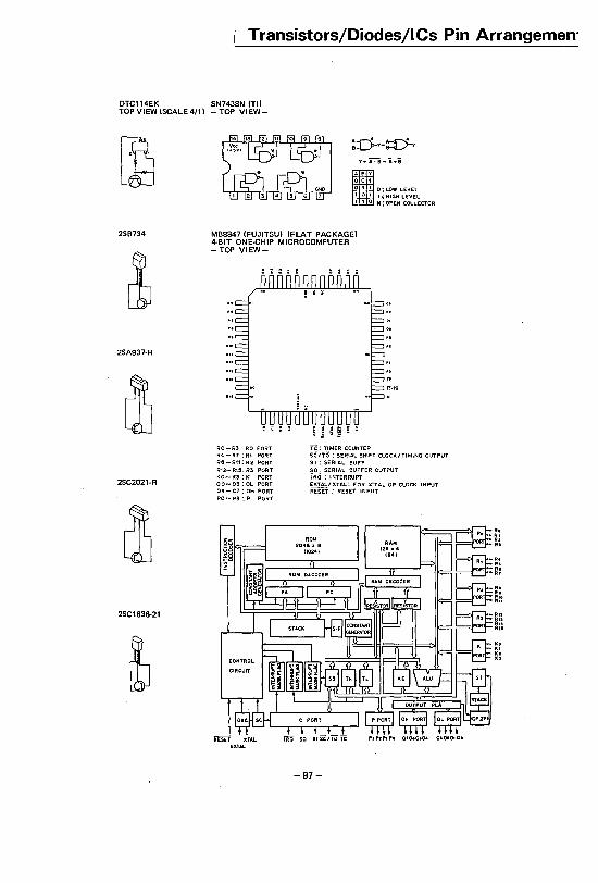
Transistors/Diodes/I Cs Pin Arrangemen1
DTC114EK SN7438N (Til TOP VI EW (SCALE 4/1l - TOP VI EW -
2SB734
2SA937·R
2SC2021·R
2SC1636-21
MB8847 (FUJITSU) (FLAT PACKAGEl 4-BIT ONE-CHIP MICROCOMPUTER -TOP VIEW-
RO-R3 :RO PORT R4-R7 :RI PORT R8-RII: R2 PORT R12- RI~: R3 PORT KO- K3 : K PORT 00- 03: OL PORT 04- 07: OH PORT PO- P3 : P PORT
iiEs£T XTAL EXTAL
fC: TIMER COUNTER sc/fQ: SERIAL SHIFT CLOCK/TIMING OUTPUT S I : SERIAL BUFF SO: SERIAL BUFFER OUTPUT iRQ : INTERRUPT EXTAL/XTAL: FOR X'TAL OR CLOCK INPUT RESET: RESET INPUT
PJP,PlPo 0.,0.0104 01010.00
-97-

MEMO
••••••••••••••••••••••••••••••••••••• ': ••••••••••••••••••••••••••••••••••••• 0 •• ~.......................................................... ••••••••••••••••••••• •••••••••••••••••••••••••••••••••• • •••••••••••
-98-

-99-

c
Sony Corporation 83K051()'1 o 9-975-131-01 © 1983
-100-
MICRO FLOPPYDISK DRIVE
SUPPLEMENT 1
This supple_ant covers so_a chenge of reference disks fer servicing of .odels OA-D32W/OA-D32Y.
We have changed signal compos it method and phase relationship for alignment disk, in order to increase
the accuracy of, the sdjustmenu to be required in the field service.
In addition to the above, system disks to be employed for both radial alignment adjustment/ measurement
and final error check are modified in each content, to utilize the field available soft-warea CP/M (SONY
model name SMW-7002) and SONY BASIC (SONY model name SMW-7011). The new system disk, we prepare,'
is named as R/E .ystm disk (OR-D1l4VA, PIN 8-960-010-18).
In the actual procedure, the following disks must be ~repared for necessary adjustment and final check.
1. As for radial alignment adjustment/measurement, a SONY BASIC and our new system disk OR-D114VA
are requited.
2. A. for final check, a CP/M disk, a CP/M disk and our new .ystem disk OR-D1l4VA are required.
The change of PIN for aDDllcable disks are .. Eolln .....
I faa PIN of o.-Iolnel disk PIN of new disk
a) AligmlCnt disk Clt-D47VA Clt-D123VA
8-960-009-32 8-960-010-26
b) Radial aliganent Clt-D86VA
syatem disk 8-960-009-74 none
c) Error check Clt-D87VA
.yatem disk 8-960-009-75 none
d) (JIIM disk none l'MV-7002
e) s:::M' BAS IC none 9ofiV-7011
f) R/E .yatem disk none Clt-D1l4VA
8-960-010-18
The following .ection. (pagca on original .ervice manual) .hould be replaced with attached reviled page ••
Section 2-1 General and special tool (page 8)
Section 3-3-1 Procudure Tuck positioning (pages 16 - 17)
Sect ion 3-4 Final check
Section '-4 Radial aliganent
(page. 23 - 27)
(pages 42 - 46)
SONY. SERVICE MANUAL
2-1 GENERAL AND SPEC I At TOOL LIST
The tools and measuring instruments for
perform maintenance on the OA~D32W/oA-D32V
are listed below.
a. General Tools
TOTSU screw driver(H2.6)
+ driver 2mm
- driver 2mm
- driver 4mm
Tweezers
Round nose plier
Adj. rod
Cutter
CP/M (SKW-7002)
SONY DISK BASIC (SKW-7011)
Soldering iron (20W)
Desoldering Hetal Braid
DC power supplier
+5VDC!5%, 0.8A min.,
+12VDC!5%, 1.5A min.
Tester
b. Special Tools
HFD Checker II
SONY parts No.
(7-721-050-62)
(7-700-749-01)
(7-700-750-01)
(7-700-750-04)
(7-700-753-02)
(7-700-757-01)
(7-700-733-01)
(7-700-758-02)
(J-609-182-0A)
SHC-70 System
SHI-7011/sHI-701lA/sHI70l2/SHI70l2A
c. Heaauring Equipment
Oscilloscope Dual. Trace 20KHz
Universal Counter Resolution O.lmsec.
Tension Gauge (Max. 200g)
Tension Gauge (Max. 20g)
d. Disu
Level Disk
ED OR-D46VA
Era OR-D46WA
Alignment Disk
ED OR-DI23VA
Era OR-D47WA
Dynamic Inspection Disk +30
ED OR-D~IVA Era 0~-D51WA
Dynamic Inspection Disk -30
(J-604-163-0A)
(7-732-050-10)
(8-960-009-31 )
(8-960-009-40)
(8-960-010-26)
(8-960-009-41 )
(8-960-009-35)
(8-960-009-44)
ED OR-D52VA (8-960-009-36)
_ OR-D52WA (8-960-009-45)
Cleaning Disk
ED OR-D29VA (8-960-009-15)
_ OR-D29WA (8-960-009-39)
e. Expendable and Chemical Supplies
Nut Lock
Alcohol
Sony Oil
Sony Grease
(7-611-018-01 )
(7-622-001-52)
SHC-70 Bamboo Stick
KX-13HGl Applicator
AID Converter (J-623-002-0A)
25P/26P Conversion Cable (J-623-001-0A)
R/E System Disk (OR-D1l4VA) (8-960-010-18)
Rotatory Knob (for stepping motor)
(J-609-011-0A)
Lead Screw Eccentricity Inspection Tool
(J-609-l36-0A)
Standard Disk Dummy (for Cassette-Up ABB'y
Installation) (J-609-120-0A)
Geared Driver (J-609-o17-0A)
Pad Weight (J-609-l24-0A)
Hexagon Wrench Torque Driver (J-609-l25-0A)
Power Cable (J-609-l30-0A)
Interface Cable (J-609-200-0A)
-2-
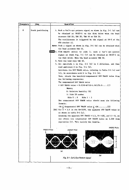
Procedure Ste
'Irack positioning
eratlon
1. Such a Cat I s eye pattern signal as shown in Fig. 3-1 (a) can
be obtained at CNI07-1 on the disk drive when the head
accesses 'IRK 20, 'IRK 30, 'IRK 40 or 'IRK 50.
The oscilloscope is triggered by the signal at 'IP-5 of the
MFD checker II.
Bote: Such a signal as shown in Fig. 3-1 (b) can be obtained when
the head accesses 'IRK 40.
EE.ra 2. SIDE SELEC'I switch to side 1. such a Cat I s eye pattern
signal as shown Fig. 3-1 (b) can be obtained at CN107-1 on
the disk drive. When the. head accesses 'IRK 40.
3. Move the head onto 'IRK 40.
4. Set amplitude L in Fig. 3-1 (b) to 4 divisions, and then
read amplitude R in Fig. 3-1 (b).
Calculate the OFF 'IRACK value, refering to 'Iable 3-1 (c) and
(d), in accordance with R in Fig. 3-1 (b).
Then, obtain the humidity-compensated OFF 'IRACK value from
the following expression:
The compensated OFF 'IRACK value
= OFF 'IRACK value + 0.2(50-H)(32-1.5S)/33.5 ••••• (1)
Where;
H: Relative humidity (X)
S: Side ID number
Side 0 : 0 Side 1 : 1
'Ihe compensated OFF 'IRACK value should meet the following
formula.
-26 :s Compensated OFF 'IRACK value $ +26 ••••••••• (2)
[EX) For R - 3.6 in the OA-D32V, the apparent OFF 'IUCK value is
as shown in table 3-1 . (c).
Assuming the apparent OFF 'IRACK - 4.5, H - 60X, and SaO, we
can obtain the compensated OFF 'IRACK value as 2.589 from
expression (1). This satisfy the formula.
INDEX Pulse INDEX Pulse INDEX Pulse
I I
(a)
(b)
Fig. 3·1 Cat's Eye Pattern Signal
-3-
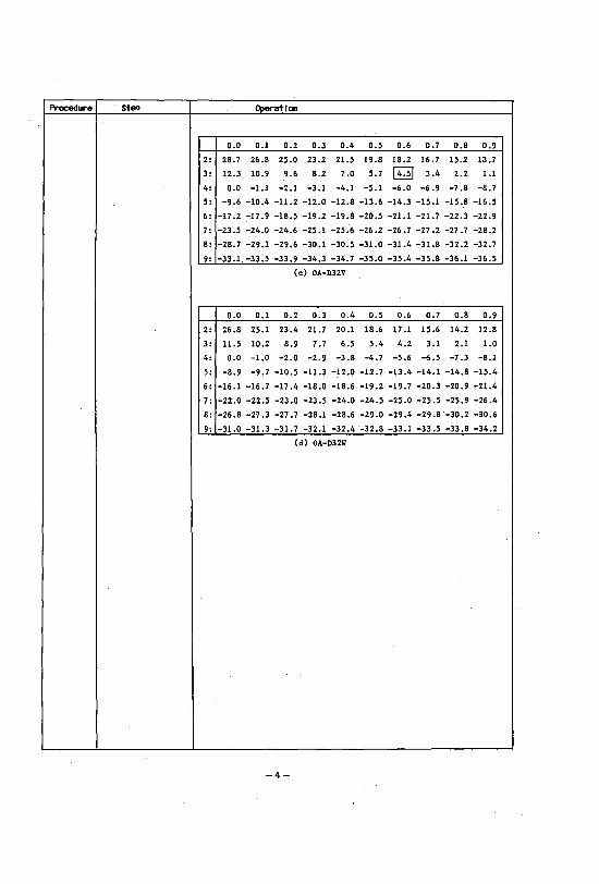
Procedure stan Operation
0.0 0.1 0.2 0.3 0.4 0.5 0.6 0.7 0.8 0.9
2: 28.7 26.8 25.0 23.2 21.5 19.8 18.2 16.7 15.2 13.7
3: 12.3 10.9 9.6 8.2 7.0 5.7 [DJ 3.4 2.2 1.1
4: 0.0 -1.1 -2.1 -3.1 -4.1 -5.1 -6.0 -6.9 -7.8 -8.7
5: -9.6 -10.4 -11.2 -12.0 -12.8 -13.6 -14.3 -15.1 -15.8 -16.5
6: -17.2 -17.9 -18.5 -19.2 -19.8 -20.5 -21.1 -21.7 -22.3 -22.9
7 : -23.5 -24.0 -24.6 -25.1 -25.6 -26.2 -26.7 -27.2 -27.7 -28.2
8: -28.7 -29.1 -29.6 -30.1 -30.5 -31.0 -31.4 -31.8 -32.2 -32.7
9: -33.1.-33.5 -33.9 -34.3 -34.7 -35.0 -35.4 -35.8 -36.1 -36.5
(c) OA-D32V
0.0 0.1 0.2 0.3 0.4 0.5 0.6 0.7 0.8 0.9
2: 26.8 25.1 23.4 21.7 20.1 18.6 17.1 15.6 14.2 12.8
3: 11.5 10.2 ' 8.9 7.7 6.5 5.4 4.2 3.1 2.1 1.0
4: 0.0 -1.0 -2.0 -2.9 -3.8 -4.7 -5.6 -6.5 -7.3 -8.1
5: -8.9 -9.7 -10.5 -11.3 -~2.0 -12.7 -13.4 -14.1 -14.8 -15.4
6: -16.1 -16.7 -17.4 -18.0 -18.6 -19.2 -19.7 -20.3 -20.9 -21.4
7 : -22.0 -22.5 -23.0 -23.5 -24.0 -24.5 -25.0 -25.5 -25.9 -26.4
8: -26.8 -21.3 -27.7 -28.1 -28.6 -29.0 -29.4 -29.8-30.2 -30.6
9: -31.0 -31.3 -31.7 -32.1 -32.4 -32.8 -33.1 -33.5 -33.8 -34.2
(d) OA-D32W
-4-
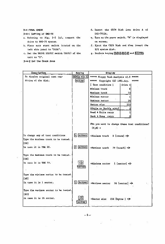
3-4 F I NAt. CHEa<
3-4-1 Setting of SIC-70
Refering to Fig. 2-2 (a) I connect the
drive to SKC-70 system.
b. Place auto start switch located on the
left side panel to "DISK".
c. Set the DRIVE SELECT switch (SlO1) of the
unit to "2".
3-4-2 Set the Check Area
Oeser I pt I on
To disp18y original test con
dition of the disk.
KevlnQ
d. Insert the CP/K Disk into drive A of
SKI-701lA.
e .• Turn on the power switch. "A" is displayed
on screen.
f. Eject the CP/M Disk and then insert the
R/E system disk.
g. Perform keying ~,f!!l,~,E!.1!l,9 and !RETURN~
Olspl8V
***** Floppy Disk Analysis v3.0 ***** ***** Copyright (e) 1981. Sep. ***** [ Test condition] drive C
Minimum track 0
Maximum track 79
Minimum sector 1
Maximum sector 16
Sector size 256
Single or Double side? S
Read & Write retry 1
Seek & Home retry 0
IDo you want to change these test conditions?
(Y,N) -
To change any of test conditions
Type the minimum track to be tested.
[EX)
[!] I RETURN I +Kinimum track 0 [track] -~
In case it is TRK 00.
Type the maximum track to be tested.
[EX)
In case it is TRK 79.
Type the minimum sector to be tested.
[EX]
In case it is 1 sector.
Type the maximum sector to be tested.
[EX]
In case it is 16 sector.
@] I RETURN I +Maximum track 79 [track] -~
+Minimum sector 1 [sector] -~
ill I RETURN I +Maximum sector 16 [sector] &~
+Sector size 256 [bytes ] -~
-5--
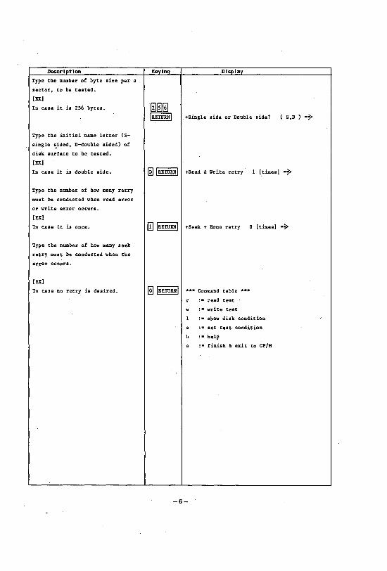
Oeser I pt I on
Type the number of byte size per a
sector, to be tested.
[EX)
In case it is 256 bytes.
Type the initial name letter (S
single '!.ided, D-double sided) of
disk surface to be tested.
[EX)
In case it is double side.
Type the number of how many retry
must be conducted when read error
or write error occurs.
[EX)
In case it is once.
Type the number of how many seek
retry must be conducted when the
err9r occurs.
[EX)
In case no retry is desired.
Keying Display
. +Single side or Double side? (S,D)·~
~ \ RETURN I +Read & Write retry 1 [times) .~
ill \RETURNI +Seek + Home retry 0 [times) .~
@] \ RETURN I *** Command table *** r :- read test
w :- write test
I :- show disk condition
s :- set test condition
h :- help
e :- finish & exit to CP/M
-6-
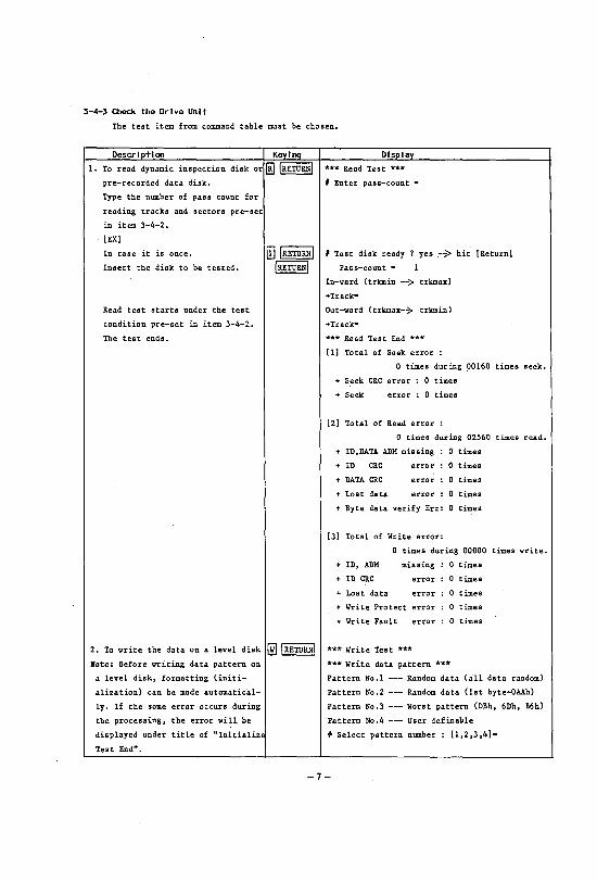
3-4-3 Check the DrIve Unl1-
The test item from command table must be chosen.
Oeser I p1-1 on KeyIng DIsplay
1. To read dynamic inspection disk or [!JIRETURN\ *** Read Test *** pre-recorded data disk. # Enter pass-count -
Type the number of pass count for
reading tracks and sectors pre-set
in item 3-4-2.
[EX]
In case it is once. # Test disk ready ? yes ,-.;:. hit [Return]
Insert the disk to be tested.
Read test starts under the test
condition pre-set in item 3-4-2.
The test ends.
Pass-count - 1
In-ward (trkmin --> trkmax)
+Track-
Out-ward (trkmax-~ trkmin)
+Track-
*** Read Test End *** U] Total of Seek error :
o times during 00160 times seek.
+ Seek eRe error : 0 times
+ Seek error : 0 times
[2] Total of Read error :
0 times during 02560 times read.
+ ID,DATA ADM missing : 0 times
+ ID eRe error : 0 times
+ DATA eRe error : 0 times
+ Lost data error : 0 times
+ Byte data verify Err: 0 times
[3] Total of Write error:
o times during 00000 times write.
+ ID, ADM
+ ID eRe
missing : 0 times
error : 0 times
+ Lost data error
+ Write Protect error
: 0 times
: 0 times
+ Write Fault error: 0 times
2. To write the data on a level disk ~ I RETURN \ *** Write Test *** Kote: Before writing data pattern on *** Write data pattern ***
a level disk, formatting {initi- Pattern No.1 --- Random data (all data random)
alization) can be mode automatical- Pattern No.2 --- Random data Ost byte-OAAh)
ly. If the some error occurs during Pattern No.3 --- Worst pattern (DBh, 6Dh, B6h)
the processing, the error will be Pattern No.4 --- User definable
displayed under title of "Initialize # Select pattern number: [1,2,3,4]-
Test End".
-7-
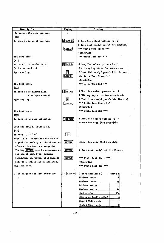
DescrIptIon
To select the data pattern.
[EX)
Key I IIQ Dlsplq
In case it is worst pattern. ~IRETURNI I Now. You select pattern No: 3
The test ends.
[EX)
In case it is random data.
(aU data randOlll.)
Type any key.
The test ends.
[EX)
In case it is random data.
Ost byte - OAAh)
Type ,any key.
The tes tends.
[E)t)
In case it is user definable.
Type the data of written it.
[EX)
Ii,. case it· is "DA".
Bote: Only 2 characters can be as-
signed for each byte; the character I RETURN I of more than two is disregarded.
The key I RETURN I must be depressed at I RETURN I the end of each byte. MaxilllUDl
twenty(20) characters (ten kind of
byte-10th bytes) can be assigned.
The test ends.
3. To display the test condition. ~ IRETURNI
I Tut disk ready? yu-~ hit [Return)
*** Write Test Start *** +Track-End
*** Write Test End ***
I Now. You select pattern No: 1
I. Hit any key after few seconds -~
I Tut disk ready? yes-~ hit [Return)
*** Write Test Start *** +Track-End
*** Write Test End ***
I Now. You select pattern No: 2
I Hit any key after few seconds -~
# Tut disk ready? yes-~ hit [Return)
*** Write Test Start *** +Track-End
*** Write Test End ***
# Now. You select pattern No: 4
+Enter hex data [lst Bytes)-3>
+Enter hex data [2nd Bytes)-~
# Tut disk ready? -) hit [Return)
*** Write Test Start *** +Track-End
*** Write Test End ***
[ Tut condition ]
HinilllUDl track
MaxilllUDl track
HinilllUDl lector
Maximum sector
. Sector size
Single or Double side?
Read & Write retry
Seek & HOme retry
drive C
0
79
1
16
256
S 1
0
-8-
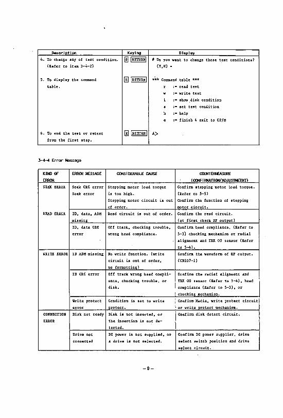
Oeser I pt I on Keying Dlspll:lY
4. To change any of test condition. [!] I RETURN I # Do you want to change these test conditions?
(Refer to item 3-4-2) (Y,N) -
5. To display the command @] I RETURN I **- Command table *** table. r :- read test
w :- write test
1 :- show disk condition
s :- set test condition
h :- help
e :- finish & exit to CP/M
6. To end the test or retest I!l I RETURN I A>
from the first step.
3-4-4 Error Message
KIND Of ERRm MESSAGE CONS IDERABLE CAUSE COONT'ERJEASlJRE
ERRm (CONF I RMATI W ADJUS1J£I101
SEEK ERROR Seek CRC error Stepping motor load torque Confirm stepping motor load torque.
Seek error is too high. (Refer to 5-5)
Stepping motor circuit is out Confirm the function of stepping
of order. motor circuit.
READ ERROR 10, data, ADM Read circuit is out of order. Conf irm the read circuit.
missing (at first check RF output)
10, data CRC Off track, chucking trouble, Confirm head compliance, (Refer to
error wrong head compliance. 5-3) chucking mechanim or radial
al ignment and TRK 00 sensor (Refer
to 5-4).
WRITE ERROR 10 ADM missing No write function. (write Confirm the waveform of RF output.
circuit is out of order, (CNl07-l)
no formatting)
10 CRC error Off track wrong head compli- Confirm the radial alignment and
ance, chucking trouble, or IRK 00 sensor (Refer to 5-4), head
disk. compliance (Refer to 5-3), or
chucking mechanism.
Write protect Condition is set to write Confirm Media, write protect circuit
error protect. or write protect mechanism.
CONNECTION Disk not ready Disk is not inserted, or Confirm disk detect circuit.
ERROR the insertion is not de-
tected.
Drive not DC power is not supplied, or Confirm DC power supplier, drive
connected a drive is not selected. select switch position and drive
select circuit.
-9-
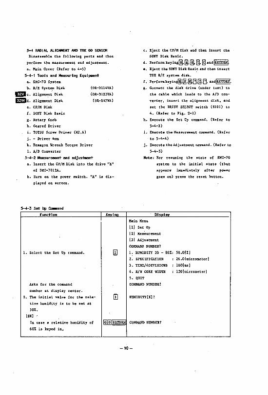
5-4 RADIAL ALIGtIEKT AND TRK 00 SENSOR
Disassemble the following parts and then
perform the measurement and adjustment.
a. Main Cover (Refer to 4-5)
5-4-1 Tools and Measuring Equlpll8rrt
a. SMC-70 System
b. RIE System Disk (OR-D1l4VA)
EDc. Alignment Disk (OR-DlZ3VA)
_d. Alignment Disk (OR-D47WA)
e. CP/M Disk
f. SONY Disk Basic
g. Rotary Knob
h. Geared Driver
i. TOTSU Screw Driver (H2.6)
j. - Driver 4mm
k. Hexagon Wrench Torque Driver
1. A/D Converter
5-4-2 Measurement and adjustment
a. Insert the CP/K Disk into the drive "A"
of SKI-70l2A.
b. Turn on the power switch. "A" is dis
played on screen.
5-4-3 Set Up CcaDand
Function Keying I
1. Select the Set Up command. [!]
Asks for the command
number at display center.
2. The initial value for the rela- [!] tive humidity is to be set at
50%.
[EX)
c. Eject the CP/M Disk and then insert the
SONY Disk Basic.
d. Perform keying[!l,~,~.I!I, @] andIRETURN~ e. Eject the SONY Disk Basic and then insert
TSE R/E system disk.
f. Perform keyingl!l,@I,~,B.[!J.B, andIRETURN~ g. Connect the disk drive (under test) to
the cable which leads to the A/D con
verter. insert the alignment disk, and
set the DRIVE SELECT switch (SI01) to
4. (Refer to Fig. 2-2)
h. Execute the Set Up command". (Refer to
5-4-3)
i. Execute the Measurement command. (Refer
to 5-4-4)
j. Execute the Adjustment command. (Refer to
5-4-5)
Bote: For resuming tbe state of SMC-70
system to the initial state (that
appears' immediately after power
goes on) press the reset button.
Display
Kain Kenu
[1) Set Up
(2) Keasurement
(3) Adjustment
COHHAND NUMBER?
1. HUMIDITY 20 - 80%: 50.0[%)
2. SPECIFICATION : 26.0 [micrometer)
3. TIHE/4DIVIS IONS : 100[ms)
4. R/W CORE WIDTH : l20[micrometer)
5. QUIT
COHHAND NUMBER?
HUMIDITY[%) ?
In case a relative humidity of ~@IIRETURNI COHHAND NUMBER?
60% is keyed in,
-10-
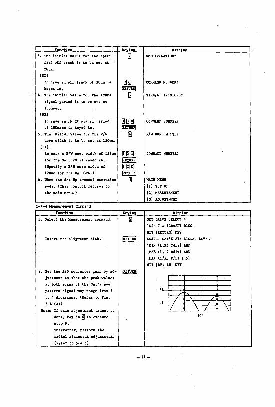
FunctIon
3. The initial value for the speci
fied off track is to be set at
26U111.
[EXI
In case an off track of 30UIII i.
keyed in,
4. The initial value for the INDEX
lignal period is to be set at
10Omsec.
[EXI
In case an INDEX signal period
of 100msec is keyed in,
5. The initial value for the R/V
core width is to be set at 120UIII.
[EXI
In cale a R/V core width of 131II1II
for the OA-D32V is keyed in.
(Specify a R/v core width of
120II1II for the OA-D32V.)
6. When the Set Up command execution
ends. (This control returns to
the main menu.)
5-4-4 Measurement Ccamlnd
FunctIon
l. Select the Measurement command.
Insert the Alignment disk.
2. Set the AID converter gain by ad-
justment so that the peak values
at both edges of the Cat' s eye
pattern signal may range from 2
to 4 divisions. (Refer to rig.
5-4 (a»
IIote: If gain adjustment cannot be
done, key in ~ to execute
Itep 9.
'lbereafter, perform the
radial alignment adjustment.
(Refer to 5-4-5)
Kevlna
~m ~ ~
[!1~~ JRETURNI
~
KeylnQ
§
~
!RETURN I
Dls~l~
SPECIFICATIOn?
COMMAND NUMBER?
TJlf1!./4 DIVISIONS?
COMMAND NUMBER?
R!V CORE WIDTH?
COMMAND NUMBER?
HAIN MENU
[11 SET UP
[21 MEASUREMENT
[31 ADJUSTMENT
DlsplZIY
SET DRIVE SELECT 4
INSERT ALIGNMENT DISK
HIT [RETURN)- KEY
ADJUST CAT'S EYE- SIGNAL LEVEL
[KIN (L,R) 2divl AND
[MAX (L,R) 4divl AND
[MAX (L/R, R/L) 1.5)
HIT [RETURNI KEY
41
/" '" / \ 21 / \ /
/ , / ral
-11-
/' ~ \ ,
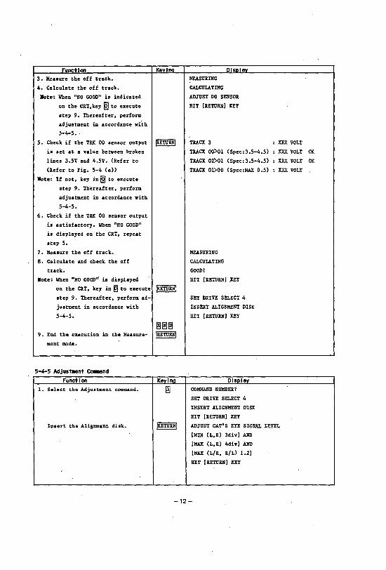
Function Keying Display
3. Meuure the off track. ~SURING
4. Calculate the off track. CALCULATING
IIote: When "NO GOOD" i8 indicated ADJUST 00 SENSOR
on the CRT,key ~ to execute HIT [RETURN] KEY
atep 9. Thereafter, perform
adjustment in accordance wi"th
5-4-5 •.
5. Check if the TRK 00 sensor output !RETURNJ TRACK 3 : XXX VOLT
is Bet at a value between broken TRACK 00>01 (Spec:3.5-4.5) : XXX VOLT OK
line8 3.5V and 4.5V. {ltefer to TRACK 02)01 (Spec:3.5-4.5) : XXX VOLT OK
{Refer to Fig. 5-4 (e» TRACK 01>00 (Spec:HAlt 0.5) : XXX VOLT
Bote: If not. key in lID to execute
step 9. Thereafter, perform
adju8tment in accordance with
5-4-5.
6. Check if the TRK 00 8en8or output
i8 satisfactory. When "NO GOOD"
iB displayed on the CRT, repeat
step 5.
7. Measure the off track. MEASURING
8. Calculate and check the off CALCULATING
track. GOOD I
.ote: When "NO GOOD" is di8played HIT [REroRN] KEY
on the CRT. key in EI to execute ~ 8tep 9. Thereafter, perform ad- SET DRIVE SELECT 4
justment in accordance with INSERT ALIGNMENT DISK
5-4-5. HIT [RETURN] KEY
l§1!@ 9. End the execution in the Measure- IRETURN!
ment mode.
5-4-5 AdJustMnt ec-end
Function Keying Display
1. Select the Adjustment command. ~ COMMAND NUMBER?
SET DRIVE SELECT 4
INSERT ALIGNMENT DISK
HIT [RETURN] KEY
Insert the Alignment disk. /RETURNJ ADJUST CAT'S EYE SIGNAL LEVEL
[MIN (L.R) 3div] AND
[HAlt (L,R) 4div] AND
[HAlt (L/R, R/L) 1.2]
HIT [RETURN] KEY
-12-
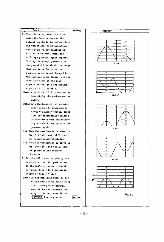
Function KeylnQ Display
2. rurn the rotary knob clockwise
until the head arrives at the
outmost position. Thereafter J turn
the rotary knob counterclockwise /" ~
while stopping and starting at / \ each clicking point until the _L \ Cat's eye pattern signal appears. / \ /' '" / '\ rurning the stepping motor with
rb)-/ the geared driver within the range
that the screw fastening the
stepping motor is not dropped from
the stepping motor flange, set the "\ /\ amplitude ratio of the peak
\ 7 , signals on the Cat's eye pattern ""- ./ f\ signal at 1 :1.2 or less. \ /
Hote: A ratio of 1 :1.2 is defined by '\. /
identifyinl\ the smaller one as Cbl-2
~nity.
Hote: If adjustment of the stepping
motor cannot be conducted by
using the geared driver,first / ~ find the appropriate position / \
/ '\ in accordance with the follow-/' :--... /
ing procedure. and perform ad- / \. 7 justment again. (c)-/
(1) When the waveform is as shown in
Fig. 5-4 (b)-l and (b)-2. turn
the geared driver clockwise.
(2) When the waveform is as shown in f\ f" Fig. 5-4 (C)-l and (c)-2. turn \ / the geared driver counter- \ 7 \... /
\ / clockwise. \ /
3. Set the AID converter gain by ad- Ie )-2 justment so that the peak values
of the Cat's eye pattern signal
may range from 3 to 4 divisions.
(Refer to Fig. 5-4 (d» 41
Hote: If the amplitude ratio is set J' / \. / '\. at any value other than utmost
/ '\ / \ I: 1.2 during initializing. 7 \ / \ control does not advance the (dl
step to the next even if the Fig. 5-4
I RETURN I key is pressed. IRETURNI
-13-
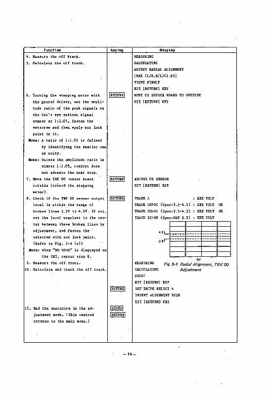
Function
4. Measure the off 'track.
S. Calculate the off track.
Keying
6. Turning the stepping motor with I RETURN I the geared driver, set the ampli-
tude ratio of the peak signals on
the Cat's eye pattern signal
utmost at 1: 1.0S. fasten the
setscrew and then apply nut lock
paint to it.
Hote: A ratio of 1 :1.0S is defined
by identifying the smaller one
as unity.
Hote: Unless the amplitude ratio is
utmost 1: 1.05. control does
not advance the next step.
7. Move the TRK 00 "lensor board
outside (toilard the stepping
motod.
8. Check if the TRK 00 sensor output I RETURN I level is within the range of
broken lines 3.SV to 4.SV. If not,
set the level nearlest to the cen-
ter between these broken lines by
adjustment, and fasten the
setscrew with nut lock paint.
(Refer to Fig. S-4 (e»
Hote: When "NO GOOD" is displayed on
the CRT, repeat step 8.
9. Measure the off track.
10. Ca'Iculate and check the off track.
11. End the execution in the ad
justment mode. (This control
returns to the main menu.)
MEASURING
CALCULATING
Display
ADJUST RADIAL ALIGNMENT
[mx: (L/R,R/L)<1.0S]
TIGHT FIRMLY
HIT [RETURN) KEY
MOVE 00 SENSOR BOARD TO OUTSIDE
HIT [RETURN) KEY
ADJUST 00 SENSOR
HIT [RETURN] KEY
TRACK 3
TRACK 00>01 (Spec:3.S-4.S)
TRACK 02>01 (Spec:3.S-4.S)
TRACK ODOO (Spec:MAX O.S)
4.SL
: XXX VOLT
: XXX VOLT
: XXX VOLT
: XXX VOLT
OK
OK
J.S r~-=-=-=-=-~-=-=-=--=~-=-=--=-=.-!=--=-=-~
(e) MEASURING
CALCULATING Fig. 5·4 Radial Alignment, TRK 00
Adjustment GOODI
HIT [RETURN] KEY
SET DRIVE SELECT 4
INSERT .ALIGNMENT DISK
HIT [RETURN] KEY
-14-
5-4-6 Error Message
One of the following errors can occur
during measurement, adjustment, or setting
of the machine for radial alignment:
a) Not Ready ••• Indicates that READY signal
is not issued. Check for disk drive
connection or check for the DRIVE SELECT
switch position.
b) No Index Pulse ••••• Indicates that INDEX
signal is not issued. Check for disk
drive connection.
c) Cat's Eye Error ••••• Indicates that the
Cat I s eye pattern signal is abnormal.
Check for the alignment disk.
In addition to these messages in above, one
of the following statements is also, dis
played.
-15-
Statecent 1: [0] CONTINUE/[l] RETRY
Statement 2: [RETURN] FIRST STEP/[l] RETRY
Key in @] when statement ill is displayed, and
then control advances the step to the next,
disregarding the error, which has occurred:
Thereafter, key in ill and then the same
measurement item is executed again.
Key in I RETURN I when statement 2 is dis
played, and then control performs the radial
alignment measurement and returns to the
initial step in the Adjustment mode. There
after, key in ill and then the same measure
ment item is executed again.
Bote: Check for the disk drive in accordance
with confirmation items to the message
displayed before retrying the key-in
ill operation.

Sony Corporation 84F0510-1
9·975·131·51 @1984
-16-

~P~_T_S_U_ST_' ______ ~I~

PARTS LIST [£J ACT PART NUMBERING SYSTEM
Comprises eight numeric digits.
ACT numbers will provide a restricted identification by major category only and no further attempt will be made to try and produce a comprehensive descriptive part number.
Material Control will maintain a register of part numbers and will be the sole authority for issuing new numbers.
The numbering system is as follows:
XXXXXX X X
II L L'Finish identification (see note).
Major category identification (see reference).
Straight sequential number from 0001 to 9999.
These two will always be 1111 (this identifies the number as ACT).
Note Finish identification. This is used to define a part
which may have several types of finishes.
Essentially the number III will be used as standard. However, options such as plating, painting ... will be defined by 121 or 131 etc.
References Major Category Reference 1 Sub Assemblies 2 Components 3 (Spare) 4 Cabling 5 Metalworking 6 Plastics 7 Packaging 8 Fasteners/Connectors 9 Drawings/Miscellaneous
Finish
1 Standard 2 Plating 3 Paint 4 5 6 Spare 7 8 9 Drawing
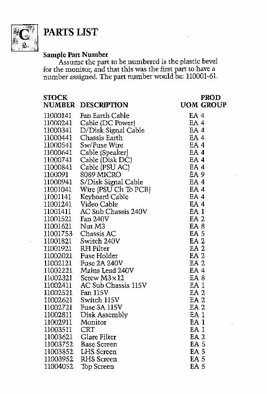
Is: I PARTS LIST
Sample Part Number Assume the part to be numbered is the plastic bevel
for the monitor, and that this was the first part to have a number assigned. The part number would be: 110001-61.
STOCK NUMBER DESCRIPTION
11000141 11000241 11000341 11000441 11000541 11000641 11000741 11000841 1100091 11000941 11001041 11001141 11001241 11001411 11001521 11001621 11001753 11001821 11001921 11002021 11002121 11002221 11002321 11002411 11002521 11002621 11002721 11002811 11002911 11003511 11003621 11003752 11003852 11003952 11004052
Fan Earth Cable Cable (DC Power) DIDisk Signal Cable Chassis Earth SwlFuse Wire Cable (Speaker) Cable (Disk DC) Cable (PSU AC) 8089 MICRO SlDisk Signal Cable Wire (PSU Ch To PCB) Keyboard Cable Video Cable AC Sub Chassis 240V Fan 240V NutM3 ChassisAC Switch 240V RFI Filter Fuse Holder Fuse2A240V Mains Lead 240V Screw M3x12 AC Sub Chassis 115V Fan 115V Switch 115V Fuse 3A 115V Disk Assembly Monitor CRT Glare Filter Base Screen LHS Screen RHS Screen Top Screen
PROD UOM GROUP
EA4 EA4 EA4 EA4 EA4 EA4 EA4 EA4 EA 9 EA4 EA4 EA4 EA4 EA 1 EA2 EA 8 EA 5 EA2 EA 2 EA2 EA 2 EA4 EA 8 EA 1 EA2 EA 2 EA2 EA 1 EA 1 EA 1 EA2 EA 5 EA 5 EA 5 EA 5
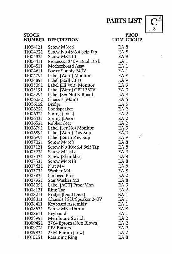
PARTS LIST [iJ STOCK PROD NUMBER DESCRIPTION UOM GROUP
11004121 Screw M3x6 EA 8 11004221 Screw No 4 x 6.4 Self Tap EA 8 11004321 Screw M3xl0 EA 8 11004411 Processor 240V Dual Disk EA 1 11004511 Motherboard Assy EA 1 11004611 Power Supply 240V EA 1 11004791 Label (Warn) Monitor EA 9 11004891 Label (Serl) CPU EA 9 11005091 Label (Hi Volt) Monitor EA 9 11005191 Label (Warn) CPU 250V EA 9 11005291 Label (Ser No) K-Board EA 9 11006052 Chassis (Main) EA 5 11006152 Bridge EA 5 11006221 Loudspeaker EA2 11006321 Spring (Disk) EA2 11006421 Spring (Door) EA2 11006521 Rubber Feet EA2 11006791 Label (Ser No) Monitor EA·9 11006891 Label (Warn) Pow Sup EA::'9 11006991 Label (Earth Pow Sup EA 9 11007021 Screw M4x8 EA 8 11007121 Screw No 10 x 6.4 Self Tap EA 8 11007221 Screw M4x12 EA 8 11007421 Screw (Shoulder) EA 8 11007521 Screw M4x18 EA 8 11007621 NutM4 EA 8 11007721 WasherM4 EA 8 11007821 Grooved Pins EA2 11007921 Star Washer M3 EA 8 11008091 Label (ACT) Proc/Mon EA 9 11008121 Ring Tag EA2 11008211 Bridge (Dual Disk) EA 1 11008311 Chassis PSU/Speaker 240V EA 1 11008411 Keyboard Assembly EA 1 11008521 Screw M3 x 16mm EA 8 11008611 Keyboard EA 1 11008991 Membrane Switch EA2 11009421 2764 Eprom (Non Blown) EA2 11009721 PP3 Battery EA2 11009821 2764 Eprom (Low) EA2 11010251 Retaining Ring EA 8
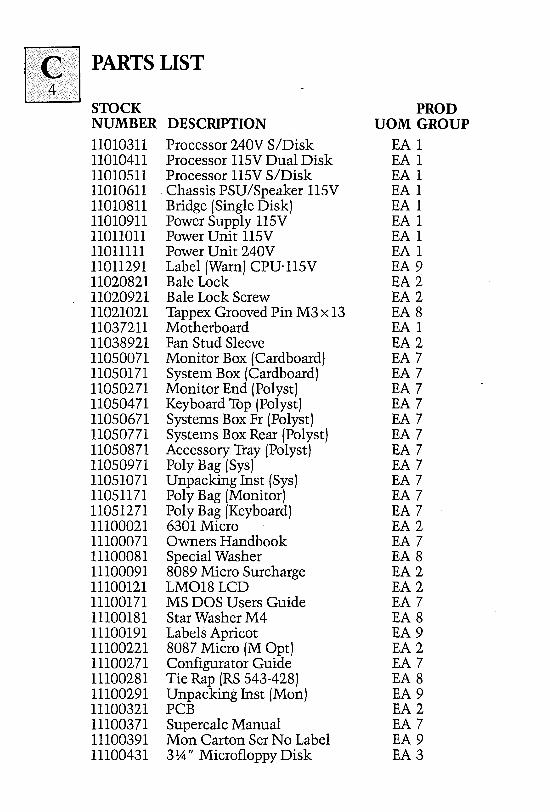
~ PARTS LIST
STOCK PROD NUMBER DESCRIPTION UOM GROUP
11010311 Processor 240V SlDisk EA 1 11010411 Processor 115V Dual Disk EA 1 11010511 Processor 115V SlDisk EA 1 11010611 Chassis PSUISpeaker 115V EA 1 11010811 Bridge (Single Disk) EA 1 11010911 Power Supply 115V EA 1 11011011 Power Unit 115V EA 1 11011111 Power Unit 240V EA 1 11011291 Label (Warn) CPU'115V EA 9 11020821 Bale Lock EA 2 11020921 Bale Lock Screw EA 2 11021021 Tappex Grooved Pin M3 x 13 EA 8 11037211 Motherboard EA 1 11038921 Fan Stud Sleeve EA2 11050071 Monitor Box (Cardboard) EA 7 11050171 System Box (Cardboard) EA 7 11050271 Monitor End (Polyst) EA 7 11050471 Keyboard Top (Polyst) EA 7 11050671 Systems Box Fr (Polyst) EA 7 11050771 Systems Box Rear (Polyst) EA 7 11050871 Accessory Tray (Polyst) EA 7 11050971 Poly Bag (Sys) EA 7 11051071 Unpacking Inst (Sys) EA 7 11051171 Poly Bag (Monitor) EA 7 11051271 Poly Bag (Keyboard) EA 7 11100021 6301 Micro EA 2 11100071 Owners Handbook EA 7 11100081 Special Washer EA 8 11100091 8089 Micro Surcharge EA2 11100121 LM018 LCD EA2 11100171 MS DOS Users Guide EA 7 11100181 Star Washer M4 EA 8 11100191 Labels Apricot EA 9 11100221 8087 Micro (M Opt) EA2 11100271 Configurator Guide EA 7 11100281 Tie Rap (RS 543-428) EA 8 11100291 Unpacking Inst (Mon) EA 9 11100321 PCB EA2 11100371 Supercalc Manual EA 7 11100391 Mon Carton Ser No Label EA 9 11100431 3 ~" Microfloppy Disk EA3
PARTS LIST [£J STOCK PROD NUMBER DESCRIPTION UOM GROUP
11100471 MS DOS Quick Ref Card EA 7 11100571 BASIC Quick Ref Card EA 7 11100671 BOS Voucher EA 7 11100771 TDI p-System Voucher EA 7 11100871 Apricot Disk Wallet EA 7 11101091 . Sys Carton Ser No Label EA 9 11101191 Apricot Insp Label EA 9 11101271 Pulsar Voucher EA 7 11443061 Monitor Top (PI) EA 6 11443161 Swivel/Ped (PI) EA 6 11443261 Mon Base (PI) EA 6 11443361 Mon Bezel (PI) EA 6 11443461 Key Top (PI) EA 6 11443561 Key Base (PI) EA 6 11443661 Sys Top (PI) EA 6 11443761 Sys Base (PI) EA 6 11443861 Sys Rear Panel (PI) EA 6 11443961 Sys Front Panel (PI) EA 6 11444561 Door (PI) EA 6 11444661 Handle (PI) EA 6 11445621 Keyboard Cable Cover (PI) EA 6 11445761 Expansion Cover (PI) EA 6 11445861 Button Disk (PI) EA 6 11445961 Battery Cover (PI) EA 6 11446061 Switch Housing (PI) EA 6 11446161 Reset Button (PI) EA 6 11446162 Brightness Wheel (PI) EA 6
.11446261 Keyboard Button (PI) EA 6 11446262 Keyboard Clip (PI) EA 6 11447061 Knob (PI) EA 6 11447161 Sys Cable Clip (PI) EA 6

""---P_O_WE_R_S_U_P_PL_X _____ ~___aIIDI
POWER SUPPLY ~ Electrical Specifications
PARAMETER MIN TYP MAX UNIT NOTES
Input Voltage 90 115 135 VAC 180 230 270 VAC
Input Frequency 47 50/60 Hz
Outputs: VOl 4.9 5.0 5.1 V +5VOutput 101 1.35 6.0 A 101 2.50* 5.0* A V02 11.4 12.0 12.6 V 102 0.60 1.50 A V03 11.4 12.0 12.6 V 103 0.40 2.10 A 103 0.75* 3.50* A V04 -11.40 -12 -12.60 V -12VOutput 104 0 0.25 A
*Loading condition if V02 and V03 are paralleled.
PARAMETER MIN TYP MAX UNIT NOTES
Efficiency 65 % At full load 115/230 VAC in
Operating Temperature 0 50 °C Ambient Temp
Ou tpu t Power 50 W Max Continuous Output Ripple 1 % 1Hzto 10 MHz Line Regulation 0.1 0.2 % Load Regulation
VOl 0.2 2.0 % V021 V031 V04 5.0 %
Over Voltage Protection 5.9 6.9 V +5V Supply
Hold-up Time 16 24 mS Full load at 115/230V
Short Circuit Loads Indefinite period on all outputs
Open Circuit Loads Indefinite period on all outputs
EMI Requirements Meets the conduction limits of VDE 0871 'B' rules for 230 VAC and FCC 'B' rules for 115 VAC in
Safety Requirements Meets UL 1012 safety standard for power supplies
EARTHING ARRANGEMENT NOTES:
AC ASSY, PIN, 110014-11 (240v) PIN 110024-11 (DEV-AS-002)
\ P/N:110004-41
(DEV-CB-006)
1. STAR WASHERS ARE REQUIRED TO ENSURE GOOD ELECTRICAL CONTACT BETWEEN TOUCHING METAL PARTS 8c CABLES.
2. LOCK NUTS PIN 11001621 (4 OFF) ARE REQUIRED ON FAN STUDS.
3. CABLE TIES PIN 11000000 (3 OFF) ARE REQUIRED TO KEEP WIRING CLEAR OF FAN BLADES.
POWER
SUPPLY
CABLE PIN: 110001-41 (DEV-CB-OOS)
CABLE pin 110002-41 (DEV-CB-OOD
CABLE PIN: 110010-41 (DEV-CB-012)
SEE POWER SUPPLY DWG FOR MECHANICAL DETAILS (DEV-AS-003)
pin 110046-11
n F ASTON ON MAIN PCB
ACT
SHEET 1 of 1
ISS. 2
DEV AS-OOl
DATE APPROVED
3118/83
17110/83
ACT
'---C_IR_C_V_IT_D_JA_G_RAM_O ___ -----'I[!]
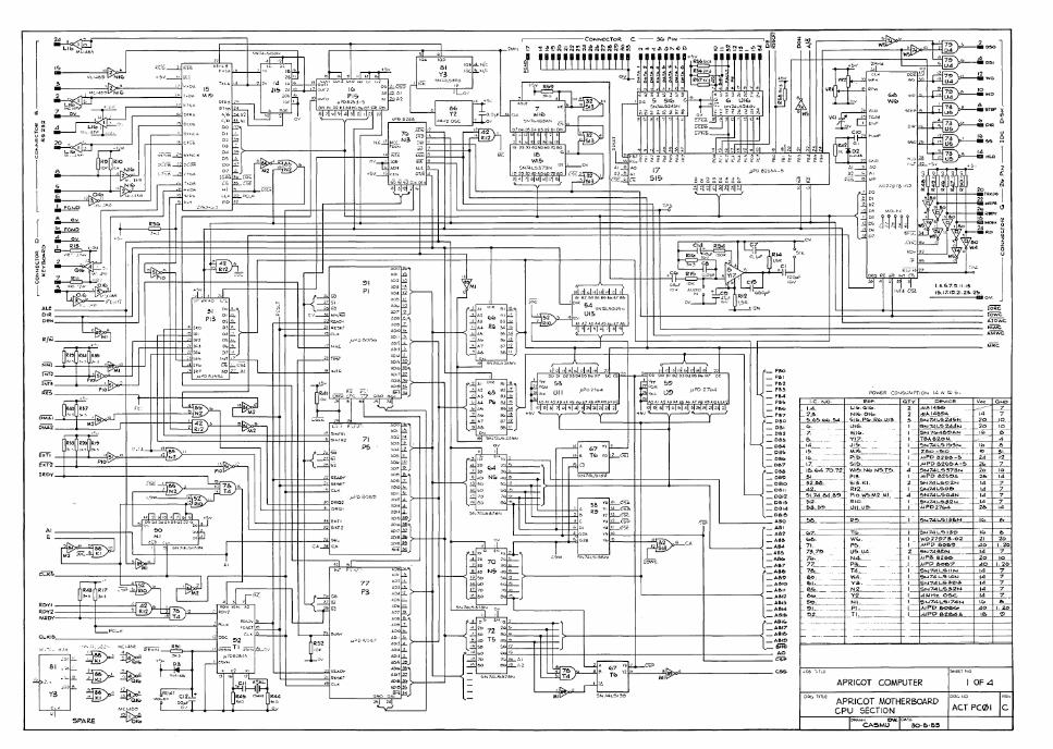
ROY' RDY2
,.
0""" BI .,~ ,"
,,,> ;z., .":.m
~3
'"' " SPARE
i--"'<-~7. " ... 70. 7~ ... "l!!'. "& .. n 7 ... a. .. '. .... ... .... ,.,. ""-!:tfZ.
"'74l.JS.1~6N
T~. , =N74L.~I~!) ,~ .. w ... , Wo27!)711o-02 20 20 .... I .uPD &0&'" 40 0.20 U~.U4. 2 SN704abN 14 7 N~. I .ups. e:ze.e. 20 10 PiL..., I PPbo&7 AO 1.20 TA. I. 7AL..SIIN WA. I 5f.,.I74,-SL4N I. 7 ,-
,~
Va.. _ I 10..1 :.4L-&a~~ ,. 7
.N2 . I SN7. L'S:!o2N 14 7 ,v- I 4MHz. osc:. I. 7 ~I. I ..... 741...,&174 ..... '" .. --P" ,.uPo> 6clbGoo 40 '.20 n. ...uPO&2.&4A. ,e. .,
'-
.... -,-
APRICOT COMPUTER I OF4
APRICOT MOTHERBOARD ACTPC01 C CPU SECTION
r~"""""CASMU DW·IC».r~30_6·e.S

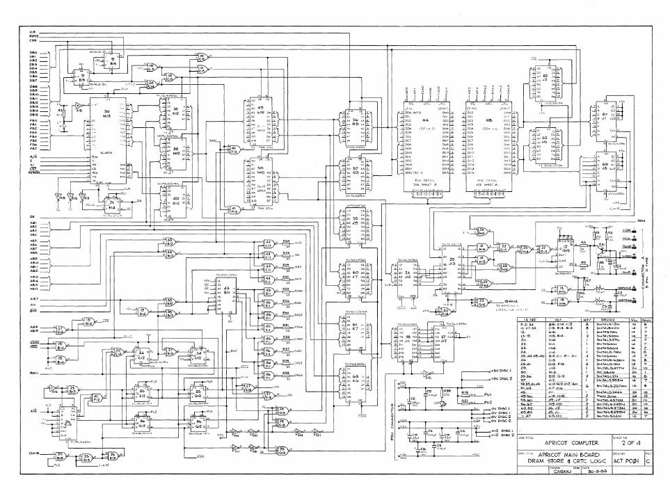
cal _ Dbll_ DB~ _
0&4_
D!!.?_ Ofl"_ O~7 _
0&6 _" Db!:l_ 0810_
Dbli_ 0&12_ OBI~_
0814_ OBI!o_
Aall _ ;---------'
Aa.2_
ASI7 ---------+++-.-------'1
~ ---------~
" ~7
HI! HII DE. 2.
r---~+~V DISC I
t-__ ~+e>v DISC '2
OV DISCI. OV DISC I OV DISC 2. ov DISC 2
20 22
25> . .d.4.A!:>,Ac"
2~
2e.:41 2~
30 Y->.3c.,;. 37.
s'" E!A.CI'2 CI:'. E\3, 81;Z
GIO. HIS.BIA
BI3 Coil ell. FI!
c,,' G13. P12
J" M'3 EI:/.o.l'2. M KI'2-:Ma,OI2--:-B.II,_
~~~ K.7.KG:.
a" 3 3
~ _____ .Ill I .4!'),<;'o. LIO,NIO· .2 ~---:-~-_=- -J~--,---J...z __ -- 2 :',~?~7_~ M",o!:l'---__ .2 ~7 J,,~J~O._~._ 2 "'!).67. ,J.;'.Jl. 2
-Li,'47. ~~.!L_ 2_
~ ~ ~
V« 5N74LS11QN '" $>-,1741..502""
.-S ..... 7.4L'S.Oc:>t-.I
,. 5/-.1741.-5:271>.1 '4 S ... 74'SION '4 5f.,I7A'i>b{:,N
5...,74$00 .... '4 5N74LSI,?36.N ,~
SN74L'SoiON ,. SN7AL..S377N 20 MC,"b4? _ 2,,--5N?4S112N I'" 5NJ~LS3!):3N . 14
SN7ALSZf,7AN ,~
S"!2AL5244N ~2_;;'_ _T-' ..... ~--_2..1
5N7.4L~37AN 20 5r::i7.4LS~-2.0
Sfo.J7.:1.L5Z'O!)N _20
S~LA_L?04p..J _14
, 'e,--
.7
+12 DISC I. "i"12 OI5C '2. f---------------,--------1
APRICOT COMPUTER
APRICOT MAIN I!>OARD DRAM STORE II CRTC LOGIC
2 OF 4

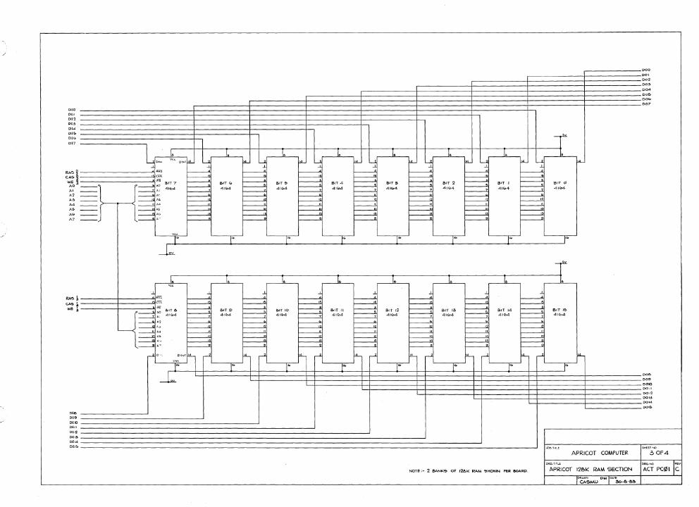
AS A~
A7
016
0110 0111
DI12
Dtl~
DIIA DIJ~
> ----------------
!. ~ e," "« DOOT~
RAs -----' I C"-S -----"
t----' .0 BIT 7 ===:::: ---Z ., 41<::>4 -------: ------" A'
~ -----" M -------1! A4 ===:! ----' " ---1.; A0 -----" l--" 0' ----'
VS~
1'"
---k.
I, "e.c
, , RA3 -----' c~~ ------"
t----' :~ &IT e. -------' 4'1>4 ~ ---'l. 0,
---" 0' -------> --""; -----" ---< -----1! A<I ------"-==:::::,,; " ------'9------" ,. ------"',
l---" " ===:21 --' 0', DOOl l .-i
"" I'· ---k
I. I. ~ La I"'-- u f------< ~ f-----------J' ~
BIT Go I ; BIT 'So I : 41«04
I : 41«>4
I • ~ f-------l'
-------" f-----------J' ~ f------" f-----------i ~
I'· I'·
], I.
~ ..!.
~ ===:;; BIT '=' ===:j I!:>IT 10 I ! 41«04 41r..4
===! f---------Z f--------"-
---" I-------a -------" f-----11. -------" f----->o ~ ===i
I ,--l !J..... ,....'-
I'· I'·
I, I, ll"-- La ~ i-----"
BIT 4 ~ BIT 3 4,0>4
t::==! AIG::04
I-------" f---------Jl ~ I ~
I'· I'·
I. I. ..!. -----.:.:
-----" ~IT II ~ BIT 1:2 41(04 41<DA
--"----"----"-
~ ~ "'- J
l'. T'"
j, I. ~ L:; i"'- ~ ~ -'
f------< t-----" f-----<' f-----.--J' I ': c--------':: I : BIT 2
I : BIT t ~
f---------Z 41<04 AICttA r-----;
I ~ r--------": r-------;'; r----" I: f---------!! t-----" f------" ~ r==::Ji I • ~ i------" f------2
I'· I'·
1. I. ,
f------< ----" I ;' f----------l' -------"
I ; BIT 13 ===:; BIT 1A r-------: 41(04 41<oA r-------:
i-------2 --"- I~ I ~ ~
---1< ~ t-----" -------"
~ ---'" ~ ~ ~ =--=-.:. !L --' "'- -' "'-, J
1" I'·
NOTE;- 2 BANKS OF r2&K RAM SHOWN PER BOARD.
_J I.
BIT ¢
4,"'4-
I'·
r I.
BIT I!::> 41(04
I'·
J06T,TLE
"'--
!J.....
APRICOT COMPUTER
DO' 002
DO'
004
DO~
DO~
007
30F4
APRICOT 12eK RAM SECTION ACT PC¢I C
B A
" " +sv " +sv
30 .30
DM 2. ,. OM 2. ,.
27
,. ,. A&12
AMINe " MRc
DMA1 23
DMAI iORc
MNc 2, " ii£5
rCiWc. 20 20 AlOWc.
a:K'5 ,. "
EXTI EXT :2
lNT3
" [NT2
" "
OBI3
AM AB3
ASJ:3
A~\::' AI'>It<>
ABle.
SHE
6MHz CLOC.K
EXPANSION I
NOTE!- MAXIMUM SIGNAL LOADIN:::::. IS
2 LS TTL GATES PER SLOT
2 EXPANSION SLOTS PER eo,A.RD.
APRICOT COMPUTER 40F4
APRICOT EXPANSION SLOT ACT PC(Z51 C
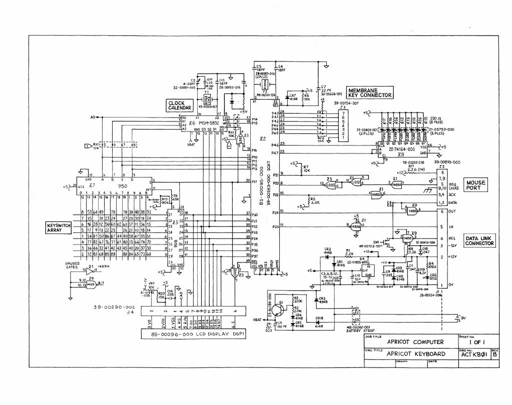
+5
AO
"""-, RXI; 5 6 7 'B~ L...!...,...o-' \OK. .... - - --'
GNO
20 vee Z7 A B D
950
e2 n~OPF lm.& -... 4-20P' F 1::20 lBPF r.-
32-00001-005 ~2!ci~ 2S-001&O-016 +
CLOCK ~~I- L CALENDAR 45-00300-027 _
18PF 28-00180-01. (2PLe5)
C4 IBPF
1-1 rn I-- C7
Y2 ~+51Z21'f I MEMBRANE I 4&0030<>124 lCR7 lR'6 3Z-0022(,-015 KEY CONNECTOR I
2 3 414B 10K .S
Xl E b .1 39-00754-007 RES J3
ll9 10,- --, r=-=- +5r"l---1--'--'--.-1Hr-r-; 4 lb 17 B ,...,,+5V
5 ~~ x1 /.2. ~% ~ :~: ~~ P14 • A2:l6 MSH-583L w~. IB 21 PIS
~!~ 28 1-, 1 ~ -Co
P4Z ;~ :::: 5
7 A3 GNO D3 OZ 01 ~~LD _J
I' 113 12 II 10 9 ~~~ N\3 ~_~ +5 0 ZZ
VBAT ~ i' 19 Pl.
Pp!! 25 1- 1 43 ~ ZI-03401-001[; -- -- -- -- -- ;;.-~-~JZ1-0575Z-000
P45 24 ~~2-r: ~ (mcS) ~-~ r~ r'S-lf~ (GPLCS) ...,. ~ .... U I; 10 11 12 l.3'
P4Gf'Z0i23'-______ '0_1< ___ '--______ ---';98 cQ~ QI Q2 Q3 + Q5 Qt.. G7 14 --'lAL 22-74164-003 vee 7
P47 rZ"'z _______________ +-=tLZ!Z: Bel £8 GND +5
+5"1 19 lB-002RZ-018 39-00619-000 'c- Rll J"z.
n 2.2n (1W) .--'-:'-+12,- 6
13_~~22-r 1~,LS:.::O::J2 .,.: ____ -:;3<:(1~9 I £ \8 REQ SUp5'--___ -.-___ ++++_--1--+-_2=t0 PH
+~ R7 10K
I-
0 {5 0 <Jl
0 8 P21 9 1
LO 0 P20 B (Jl J, 0 <0 r--------'-'''''''~ II ~ 9,10 CHAS
f"'-----.-----------'14148SA):>6"---------l3,4 ACK HY~~l-'lI~--,
01 Z345b789ABJ
12. 13 14 15 1& 17 16 19 i 2. 3 ~8 o;~o"o R1D ~~K 0 III
P2Z 10 0 8 1
-00. BOb en (l)
8 +5 ~19
53 (,4 49 78 793948 38 52 1 II R~;f'-'B,,-_-+-+-+-+_-+_~3"-17 P30 7
d> '" +5 ~~73K [~9---'-1 ~--,.l,,-9----i~ DATA
PZ4f!1:.2 ___ ;_c?-I ________ -= _____ -; __ 34511+B8+B8).I):o(,"---t~ OUT
+5 ,. Rl
P23!-"1'------------->S"'(I+8:l1A!l1'0'-----t---------l KEYSWITC H 6 35 31 2324 27203019 34 2 1ZZS 02 t7 'b P31
16 28 12 59 60 62 &3 57 11 56 15 3 13 03 '6 35 P32 5 IN ~RRAY 5 17 9 13 22 25 2& 21 to IS 14 <- J4 0 15 34 P3~
1 4 3
5481 50 8687 44905847 5551 (, 15 05 14 33 PH
71 82677677 61 80 75 067470 7 16 g Db 13 32 P35
36463241 42 43 45 40 29 37 33 a 17 07 IZ 31 P3b
L 72 83 68 85 88 89 84 65 73 69 9 18 08 II 30 P37
CR2 4148
7 ~7Z9 t ~3 4- RES
SWI -l 'm1i'" 37-00413-004 48-00103-000 ~ I~R8 :!oels 3 -12V
f1K T12-+t ~2.2K ~.047 2 +12V
UNUSED GA~B9A
19 vee GND 2 3 +5Jt4J ~ 7 -JL1,~ Z3
3B OSS ~Q~ VCCVCS ~ ~ z ~'4148 IN r--:: eR9 =Cl ~70n
lCRl 22-0180~~t05 -IV_~,...J_71, R4
~ 9_1~
10.13 1466 8,11
39-00290-002 J4
2JJ 10 t5
I
I
17 fl 109 15 1'- '+5 15-17_03~::= =?10r' 3 4148 - 51,2
+5; ... + ___ :-:-~-.-_-.,--'l2 ouT :!:~~:"414B.rO+7 T g'f" C3_&.8.12. I l. e10 ND T033 CRe . _ eRG
~:'-OOH1-0041 13 • fI
7 PLt;S 3J.-OOltlv '3l-00iB-004 'll-0047i-oOlt- , OV ll-00475-0li J'1I
CR3 4148
39-00754- 006, I I I ~! QI ~10K
':3 R2. .... E1 ~ 270( r:.Ei1 I ~ CR4 I I I .L-
VBAT~ ~48 L __ ~C~R-'8----+-----~'+~B~:------------------------------~I---~~+9V 2~- +Cll .,eRS " C_ -J I
l 85- 00096- 000 LCD DISPLAY DSP1J
b~~ t 'OD !'F r414B 4148 48-00Z~-OOl I
BAITERY 5r~~:~:~~~IT-L.----------------------------.. s~H=.IT~~~O-. ______ ~ APRICOT COMPUTER I OF I
DRG TITLE
APRICOT KEYBOARD OA:GNo.
ACTKB¢I REV.
B