Embed Size (px)
Citation preview
APPLYING TCAD TO EMERGING TECHNOLOGIES
by
Derek C. Lee
Memorandum No. UCB/ERL M95/38
20 May 1995
ELECTRONICS RESEARCH LABORATORY
College of Engineering University of California, Berkeley
94720

APPLYING TCAD TO EMERGING
TECHNOLOGIES
by
Derek C. Lee
Memorandum No. UCB/ERL M95/38
20 May 1995


ii I
Dedication I I To my parents with deep appreciation and respect for their support, love, an throughout my education.
guidance


iii
Acknowledgment
I would like to thank my research advisor, Professor Andrew R. Neureuther, for his encouragement, and guidance in all aspects this project. Without his contribution tion of this project would not have been possible. Even with his incredibly busy he always had free time for me. I would like to thank Professor Roger T. Howe for
this report and for his guidance on on the MEMS side of this project. I would thank my family and friends who have given me unending support and encourag the years.
For the lithography part of this report, I would like to thank Michael Ye invaluable support and expertise, and Obert Wood for his input, use, and te modified versions of SPLAT.
For the hIEMS side part of this report, I would like to thank Robert Wang for in the area of TCAD, Andrej Gabara for making my job much easier with his e
to SIAlPL System 6, and Joe Kung of Analog Devices for pushing the SIMP new limits.
The financial support for the lithography part of this project was provided conductor Research Corporation via SEhil ATECH grant 90-RIC-500 and by t vanced Lithography Program under the guidance of Dave Attwood at Law Labs. The funding for the hIEh4S part came from the ARPA zMEhlS project. are gratefully acknowledged.

Contents I
1 Introduction
2 EUV (Soft X-Ray) Image Simulation for Projection Printing 2.1 Introductjon . . . . . . . . . . . . . . . . . . . . . . . . . . . . . . . . . . . . 2.2 Zernike Polynomial Interface in SPLAT . . . . . . . . . . . . . . . . . . . . . 2.3 Wave Front. Map Interface in SPLAT . . . . . . . . . . . . . . . . . . . . . . 2.4 Integration Scheme . . . . . . . . . . . . . . . . . . . . . . . . . . . . . . . . 2.5 hlodeling Illumination Schemes . . . . . . . . . . . . . . . . . . . . . . . . . 2.6 Image Quality Stmudies . . . . . . . . . . . . . . . . . . . . . . . . . . . . . . 2.7 Conclusion . . . . . . . . . . . . . . . . . . . . . . . . . . . . . . . . . . . . .
3 3 5 6 8 9
10 12
1
. . . . . . . . . . . . . . . . 16 Bibliography . . . . . . . . . . . . . . . . . . .
3 Simulation of Non-uniformities in Sources and Optics in Projection
ing 3.1 Introduction . . . . . . . . . . . . . . . . . . . . . . . . . . . . . . . . . . . . 3.2 Optical Transmission with Apodization . . . . . . . . . . . . . . . . . . . . .
Verification of the OTA model on SPLAT . . . . . . . . . . . . . . . . OTA Effects on Image Quality . . . . . . . . . . . . . . . . . . . . . .
3.3 Arbitrary Illumination Sources . . . . . . . . . . . . . . . . . . . . . . . . . . 3.3.1 Operation and Implementation . . . . . . . . . . . . . . . . . . . . . . 3.3.2 Effect of Source Shape on Image Quality . . . . . . . . . . . . . . . .
3.2.1 3.2.2
3.3.3 Multi-element sources . . . . . . . . . . . . . . . . . . . . . . . . . . . 3.4 Conclusion . . . . . . . . . . . . . . . . . . . . . . . . . . . . . . . . . . . . .
Print- 17 17
15 19 20 21 21 26 25
29 Bibliography . . . . . . . . . . . . . . . . . . . . . . . . . . . . . . . . . . . .
4 MEMS Process Simulation using SIMPL 4.1 Introduction . . . . . . . . . . . . . . . . . . . . . . . . . . . . . . . . . . . .
4.1.1 Motivation for Simulation . . . . . . . . . . . . . . . . . . . . . . . .
30
31
:31
31
CONTENTS V
5 Conclusion
A File Structure of SIMPL System 6
B MICS Process Flow
C Etching in SIMPL
D Test Structure Generator Commands
4.1.2 Project Overview . . . . . . . . . . . . . . . . . . . . . . . . . . . . . 4.2 Overview of SIMPL System 6 . . . . . . . . . . . . . . . . . . . . . . . . . . 4.3 Simulation of MEMS Process Flows . . . . . . . . . . . . . . . . . . . . . . .
4.3.1 Overview of Simulation Cases . . . . . . . . . . . . . . . . . . . . . . 4.3.2 MICS . . . . . . . . . . . . . . . . . . . . . . . . . . . . . . . . . . . 4.3.3 Side Wall Beam Process . . . . . . . . . . . . . . . . . . . . . . . . . 4.3.4 BiMOS Technology . . . . . . . . . . . . . . . . . . . . . . . . . . . . 4.3.5 Metal Beam Process . . . . . . . . . . . . . . . . . . . . . . . . . . .
4.4 Fabrication Test Structures . . . . . . . . . . . . . . . . . . . . . . . . . . . . 4.4.1 Residue Problem . . . . . . . . . . . . . . . . . . . . . . . . . . . . . 4.4.2 Test Struct.ure Layout . . . . . . . . . . . . . . . . . . . . . . . . . . 4.4.3 Simulat. ion . . . . . . . . . . . . . . . . . . . . . . . . . . . . . . . . .
4 .5 Future Work . . . . . . . . . . . . . . . . . . . . . . . . . . . . . . . . . . . . 4.6 Conclusion . . . . . . . . . . . . . . . . . . . . . . . . . . . . . . . . . . . . .
Bibliography . . . . . . . . . . . . . . . . . . . . . . . . . . . . . . . . . . . .
I 62
32 32 33 33 34 41 47 49 52 52 52 53 57 58 60
63
71
I 72

List of Figures
2.1 2.2 2.3
2.4
2.5 2.6
Projection X-Ray Lithography using composite pupil function Pupil function represented using multiple high-order Zernike polynomials Strehl ratio for the first 36 Zernike polynomials . . . . . . . . . . . . . . Interfacing X-Ray Optics with SPLAT . . . . . . . . . . . . . . . . . . SPLAT table lookup, grid structure and implementation . . . . . . . . . A ) Imaginary and B) real parts of the pupil function when including thin-31m interference effects. . . . . . . . . . . . . . . . . . . . . . . . . . . . . . Table lookup speed improvement for the thin-film code . . . . . . . . . Intensity cutline for a 0.25 pm line/space pattern for the source in the A ) B) 3, C) 9, and D) 6 o’clock position. . . . . . . . . . . . . . . . . . , . The composite aerial image is the average of images in the previous figure.
. . . . .
2.7
2.8
2.9
2.10 Superposition of aerial images from 8 source positions and the average
2.11 Aerial images for a 0.25 pm contact for the source in the A ) 12 B) 3 C) 9 D) 6 o’clock position. . . . . . . . . . . . . . . . . . . . . . . . . . . . . .
2.12 The composite aerial image is the average of the aerial images in the pre\*.ous figure. . . . . . . . . . . . . . . . . . . . . . . . . . . . . . . . . . . . . . . .
2.13 Aerial images for a 0.25 pm elbow for the source in the A ) 12 B) 3 C) 9 D) 6 o’clock position. . . . . . . . . . . . . . . . , . . . . . . . . . . . .
2.14 The composite aerial image is the average of the aerial images in the
. . . . . . . . . . .
. .
. . 12, . .
. in-age
and . .
and . . .
3.1 Aerial image for a contact at various levels of attenuation: A ) not normalized B) normalized to open field intensity . . . . . . . . . . . . . . . . . . . .
3.2 OTA effects on mask edge intensity: A) OTA = 1 B) OTA = 1 - 0.25~’ . 3.3 Feature size dependent OTA effects for isolated transparent lines and
3.4 Feature size dependent OTA effects for isolated opaque lines and contacts
3.5 Various geometric primitives used to define the illumination source . . . . 3.6 ’ Contour plot of input intensitj. matrix with a radial]!. distribution . . . .
4
5
. .
. . con‘acts
. .
. .
. .
7 8
9 10
11 11 12
13
13
14
14
19 20 21 22
23 ’ 3
LIST OF FIGURES vii
3.7 Illumination Source . . . . . . . . . . . . . . . . . . . . . . . . . . . . . . . . 3.8 Illumination Source for Radial Distribution . . . . . . . . . . . . . . . . . . . 3.9 Comparison of Discretized Source With Uniform Distribution and Norma
Source . . . . . . . . . . . . . . . . . . . . . . . . . . . . . . . . . . . . . . .
24 25
25
3.10 Linear Intensity Distribution: Imaging Thru Focus . . . . . . . . . . . . . . . 3.11 Implementation of arbitrary source illumination . . . . . . . . . . . . . . . . 3.12 Quadrapole illumination: Feature orientation effects for periodic lines (kl=0.707).
Source in A) is rotated by 45 degrees in B). 3.13 Aerial images for A) vertical scan line sources B) left tilted scan line sources
4.1 Part.ia1 layout of a resonator showing a cutline through an anchor and dimple 4.2 Cross section of a resonator showing dimple and anchor using primitive et,ching 4.3 Cross section of a resonataor showing dimple and anchor using undercut etching 4.4 Cross section of a resonator showing dimple and anchor using rigorous et,chir.g 4.5 AlICS full view before final release . . . . . . . . . . . . . . . . . . . . . . . . 4.6 AlICS zoom view before final release . . . . . . . . . . . . . . . . . . . . . . 4.7 Example of stringer problems in the MICS process . . . . . . . . . . . . . . . 4.8 SEA4 cross section of MICS Poly-3 process . . . . . . . . . . . . . . . . . . .
. . . . . . . . . . . . . . . . . .
26 27
27 28
36 36 37 37 38 39 40 42
4 .9 SEhl top and side view of AlICS Poly-3 Process 4.10 MICS Poly-3 Process without using SOG planarization 4.11 AlICS Poly-3 Process utilizing SOG planarization
. . . . . . . . . . . . . . . . . . . . . . . . . . . .
. . . . . . . . . . . . . . .
43 44 44
. . . . . . . . . . . . . . . . . . . . . . . . . . . . . . 4.13 Cross section through beam 4.14 Cross section through anchor . . . . . . . . . . . . . . . . . . . . . . . . . . 4.15 Cross section through anchor and beam . . . . . . . . . . . . . . . . . . . . 4.16 ADXL50 before release etch . . . . . . . . . . . . . . . . . . . . . . . . . . 4.17 ADXL50 after 160s of etching 4.18 ADXL5O after 240s of etching 4.19 ADXL50 after 500s of etching 4.20 Simulation modeling effects of resist flow
4.21 Simulation without modeling effects of resist flow
4.23 Micromachined angular accelerometer: SEMs of the polJdicon capacitors .
4.25 Lithography simulation with SIAIPL . . . . . . . . . . . . . . . . . . . . . . . 4.26 il\lEhlIS Circular fabrication test structures . . . . . . . . . . . . . . . . . . .
. . . . . . . . . . . . . . . . . . . . . . . . . .
. . . . . . . . . . . . . . . . . . . . . . . . .
. . . . . . . . . . . . . . . . . . . . . . . . .
. . . . . . . . . . . . . . . . . . . . . . . . . . . . . . . . . . . . . . . . . . . .
. . . . . . . . . . . . . . 4.22 SEM of metal beam process . . . . . . . . . . . . . . . . . . . . . . . . . .
4.24 iMEMS Fabrication test structures . . . . . . . . . . . . . . . . . . . . . . .
46 46 46 48 48 48 49 50 50 51
. 52 53 55 56

Chapter 1
classified as Technology CAD (TCAD) tools-are not nearly as well established but coming increasingly more important as new technologies emerge with new levels of
complexity. Two such technologies which stand to benefit from TCAD applications are (Extreme Ultra Violet) project lithography, and fabrication of MEMS (MicroElectrohlechan- ical System) devices. Creation and application of simulation tools for these technologks the focus of this project.
This report is divided into two main parts consisting of three chapters. Chap,.ers and 3 discusses the use of lithography simulation for EC\’ projection lithography, in simulation was carried out with the SPLAT program. The second part , consisting of
4, discusses research related to process simulation of h4EhlS devices using the SIhlPL 6 simulation software.
Introduction
a:e be- p:.ocess
ELI\’
are
2 which
Chapter S:,stem
Computer-Aided Design (CAD) of integrated circuits is well established. possible to design a complex circuit, without, circuit. simulation. out, schematic capture, circuit extraction, layout automation, etc. Process
It is near Tools exist for

Chapter 2
EUV (Soft X-Ray) Image Simulation Projection Printing
Abstract SPLAT (Simulation of Projection Lens Aberrations via TCCs) has been gener- alized for exploring image quality in a projection EUV (soft x-ray) lithography proto-type system. Extensions were made in SPLAT to encompass the detailed wavefront data from the as built soft x-ray elements as synthesized in the sys- tem configuration by T. Jewel1 in Code V. Initially, 36 Zernike polynomials were used to describe the pupil function. but the image quality was overly optimistic. The detailed wavefront map from Code V on a 64x64 rectangular grid was then used. A table lookup approach with a rectangular grid and area weighting which can also simulate amplitude variations across the pupil was used in the integration. The thin arc for the undulator source path in the il- lumination was found to be best treated as a direct path integral rather than the limiting case of annular illumination. At x-ray wavelengths (13 nm) the surface figure errors of the multi-layer mirrors in the initial exploratory slrstem were quite significant and the images were primarily degraded by the variation in their position rather than their quality as the undulator is swept through its arc. This is in agreement with the experimental observations reported by 0. Wood e t . a1 and is shown to be even more severe for 2D patterns.
2.1 Introduction
A serious technology issue in the fabrication of projection extreme ultra violet (EU\’) x-ray systems is the development of multi-layer reflective mirrors whose surface tolf relative to the wavelength are adequate. Simulation of surface figure and coating effel allow system designers to specify tolerances on optical elements in the context of s\.stc
formance. While simulation of system effects in 1D is possible in Code [Opt]. the t
or
r soft mces s will 1 per-
nsfer

4 EUV (Soft X-Ray) Image Simulation for Projection
rt
Composite Pupil Function
Figure 2.1: Projection X-Ray Lithography using com- posite pupil function
of the composite pupil function to SPLAT [TNSi'] allows studies of 2D imaging. In is also possible to simulate phase-shift masks, off-axis illumination, lens filters, thin- penetration interference effects, and aperture stops. The images within the thin- and materials from SPLAT can also be coupled with SAMPLE3D [KKHTSSI] I for simulation of the resist profile time evolution and development.
A conceptual drawing of a projection x-ray system is shown in Figure 2.1. 1 pilmap of an initial exploratory optical system used by 0. Wood e t . a1 at A Laboratories [ORWJ89] illustrates the high degree of aberration in the pupil func pupil function was synthesized in Code V by T. Jewel1 from wavefront measurem individual optical elements. A pencil beam from the undulator illuminates the m then diffracts the pencil beam into a number of spots. These spots pass through ti specific locations and approximately lie on a plane in the exit pupil. If the normal of is rotated with respect to the zeroth order incident beam, a lateral shift is impar mask pattern perpendicular to the line direction when it is imaged at the wafer.
of t i l t , or equivalently the relative path difference along the spots, determines t l of the image shift. When the source position is changed, as in a rotating undula
system, the diffracted spots will pass through an entirely different region of the pup
Printing
;PLAT it ilm resist Im resist 3 \ 1 5 ?; 9 I ]
ere a pu- '&T Bell ion. The nts of the tsk which : pupil in :his plane ed to the he degree 1 se\-critj*
or source
i functioii
I

2.2 Zernike Polynomial Interface in SPLAT
Figure 2.2: Pupil function represented using multiple high-order Zernike polynomials
and a different shift will occur. This image shift effect has been simulated with SPLl will be shown t,o be more significant than the degradation of the individual image qua a given undulator position.
This chapter begins with the Zernike polynomial representation of the pupil fi which is followed by sections on the wavefront map interface and integration schemt
approaches for modeling the illumination system are then discussed. Finally, sim results from an image quality study are presented.
2.2 Zernike Polynomial Interface in SPLAT
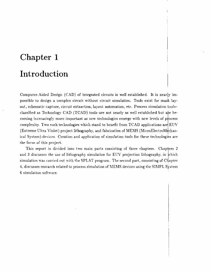
SPLAT has been generalized to represent the pupil function using an arbitrary nun Zernike polynomials, which are commonly used in representing high-order aberration in optical systems [BWSO]. Zernike polynomials are mutually orthogonal over t,he unit and thus the mean-square distribution of the wavefront relative to a Gaussian reference phere can be computed as a summation of the Zernike polynomial coefficients wit,hout need ng t,o handle cross-terms. To represent the pupil using Zernike polynomials, a file containi g the values for the multipliers is specified. A plot. of the pupil function using mult,iple high order terms can be generated by SPLAT as seen in Figure 2.2.
Currently a maximum of 64 Zernike polynomial terms may be used. However, SP AT is
ext,ensible to a higher number of terms in that the Zernike polynomial generating f u n d n has i
5
I' and ty for
iction Two
lation
ffects I" ircle, Of

6 EUV (Soft X-Ray) Image Simulat ion for Pro jec t ion
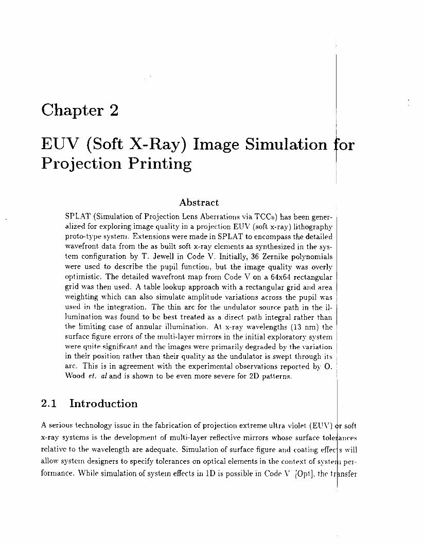
A schematic representation of the interface between a projection system, Code \' and is illustrated in Figure 2.4. Interferometry measurements are performed on the lens elements for input into Code V. The composite pupil map synthesized by output into a file which splits the pupil in three sections. This file is input into which can produce a 3D plot of the pupil as seen in Figure 2.1. Alternatively, the function can be represented by a sum of up to 64 Zernike polynomials by the for each polynomial. Normalization can be specified as either the RRlS or mas across the pupil. Using the input pupil function and an arbitrarj. mask pattern. versus linewidth along a cutline and contour plots of 2D images can be produced.
been incorporated into the SPLAT code rather than typing in all the polynomials The Zernike polynomials can be expressed as
SPLAT individual Code \. is
SPL.L\T aberration
mu1:ipliers in aberration
intensity
v,'(p sin e, p cos e) = ~ ; ( p ) exp"'
where the radial polynomials satisfy the following relation.
? r in t ing
Ixplicitly.
This provides the flexibility of using any number of terms with minimal When many terms are used, evaluation of the pupil function requires a large putation. Instead of reevaluat,ing the pupil function during the calculation of cross coefficients (TCCs), the values are stored in table. This table is also
The normalization of the Zernike polynomials was verified by taking the can be expressed as in Equation 2.3 for small non-periodic features and It is the ratio of the int,ensity at the center of a small non-periodic pin hole
the other SPLAT ext,ensions that will be described in the following sections.
aberration present.
Strehlratio E exp -4n202 - - ~ntensity(orO)a*errarcd (2 .3)
Intensity(o,O)nctaberroted
2.3 Wave Front Map Interface in SPLAT
2.3 Wave Front Map Interface in SPLAT
SPLAT
I 1 Projection X-Ray Syslem
AT&T
CODE V Q Pupil Functio 0
Figure 2.4: Interfacing X-Ray Opt,ics with SPLAT
7

8 EUV (Soft X-Ray) Image Simulation for Projection
SPLAT has been recently extended to include thin-film interference effects for within photoresist (MSYN931. This extension utilizes the same internal table l o o k ~ p ture to store complex values. Because the values are complex, the amplitude as phase of a wavefront can be represented. Thus the change in the magnitude as phase of reflectivity of a multilayer mirror due to variation in the incident angle of can be simulated. This may be particularly useful for x-ray system elements difficult to fabricate the correct multilayer d-spacing variation with angular changes the elements. A plot of the real and imaginary parts of the pupil function for imaging within the photoresist is shown in Figure 2.6. The table lookup speed when using thin-film code is shown in Figure 6. When the simulation area is sma
square area or less) the simulation time is dominated bj' the 100 seconds i t takes I O
8 I
imaging struc-
well as the w-11 as the t:ie source
w'iere i t is across
i1 case of impro\.emtnt
1 ( 5 A) calculate
A @ O Z 0 O + A O l Z 0 l + A l@z*@ + A l l Z l *
A.0 + A o l + A 1 O + A l l z (1.1) =
I,f
Figure 2.5: SPLAT table lookup, grid struc- ture and implementation
2.4 Integration Scheme
A table-lookup of the pupil function was required to input the wavefront data. The of the grid and interpolation scheme associated with this table-lookup approach art Figure 2.5. During simulation the values are interpolated using a "weighted-arez Originally linear interpolation was employed which caused convergence problems dL
action with an adaptive/self-checking algorithm used in test the numerical integr; weighted area (quadratic interpolation) scheme overcame the original convergencc Typically a 64x64 grid is used, although more dense grids can be specified.
?rinting
structure shown in ' scheme. I to inter-
lion. The problem.

2.5 Modelinn Illumination Schemes
- -
n-
L
v
II
1
Figure 2.6: A) Imaginary and B) real parts of the pupil function when including tl film interference effects.
the elements in the table lookup. For the EUV (soft, x-ray) imaging t,he dat,a for thl lookup come from Code V and the computation time is similar to the line labeled "M Thin-Film" in Figure 2.7.
2.5 Modeling Illumination Schemes
Two techniques have been used to simulate the proto-type system used by it'ood et . which a pencil beam from an undulator source is incident on a two mirror rotator tl a cone of illumination. Both annular and multiple spot illumination with a uniform a distribution have been used. Annular illumination requires much more computatior This is because integration over the annulus is computed by subtracting the results integration over the inner aperture from that of the integration over the outer aperturc to the very small 0.0004 annulus rim size, this was found to require these integrals carried out to an accuracy of 4 decimal places.
In spot illumination, integration is performed only over the small source for each pc This also allows the quality of the composite image to be compared with that from ind spot locations. The computation for N spots, requires N times as much computatioI Once the number of spots is specified, SPLAT is run for source positions that are uni distributed (equiangular separation) within the aperture at the specified radius. The cc ite image is generated by averaging the images €or each source location. The spot ap

10 EUV (Soft X-Ray) Image Simulation for Projection
f 1
lot04 -
- 100x100 Grid
loo - Thin-Film Table Looku
Without Thin-Film
Number of Harmonics in 1D
Figure 2.7: Table lookup speed improvement
brings up the interesting question as to how many spots are required to approxin tinuous arc. The underlying significance is that, in a system with a highly aberrz many different mask illumination angles should be used to average out the spot to : variations.
2.6 Image Quality Studies
The experimental pupil function shown in Figure 2.1 was used to simulate a line/space pattern for a 0.0835 NA system at 13 nm. To see the spot location efft
lation runs using different source positions have been used. The aerial image for f positions are shown in Figure 2.8. Figure 2.9 is the composite aerial image forme aging the four. The image quality at the various positions varies, but more impor images are shifting left and right relative to one another. Consequently, the compc image is wider and lower in contrast than any of the images for individual source
The effect of the image shift for 8 source positions is illustrated in Figure 8 with images for eight source positions superimposed on one another along with the image (black solid line). Control of which source positions are used in imaging w
the use of only the ”sweet” source locations and elimination of the positions th i unwanted shifts or inferior images resulting in a superior composite image.
The effect of image shift is much worse in 2-D because the shift can occur in
Printing
te a con- ed pupil, lot image
0.25 pm ts, simu- i r source by al’er-
mtlg, the ite aerial )osi t ions.
he aerial omposite uld allow produce
wo inde-

2.6 Image Quality Studies
0.25 urn Line & Space Pattern 0.25 um Line & Space Pattern
0 2 0 4 0.6 0 1
PodUon (mm)
0.25 urn Line & Space Pattern
Podtion (mn)
0.25 urn Line & Space Pattern
02 0.4 0.6 0.8 0.2 0.4 0.6 oa Position (um) Podtion (urn)
Figure 2.8: Intensity cutline for a 0.25 pm line/space pattern fo the source in the A ) 13, B) 3, C) 9, and D) 6 o’clock position.
0.25 urn Line & Space Pattern I S
1 1 ’ - Y -
I I I I
O6 0 2 0 4 0 6 0 8 1
Figure 2.9: The composite aerial image is the average of images in the previous figure.
Position (um)
11

12 EUV (Soft X-Ray) Image Simulation for Projection
It 0.25 urn LLne & Space Pattern
Position (urn)
Figure 2.10: Superposition of aerial images from 8 source positions and the average im- age
pendent directions. These 2D effects are illustrated in Figures 2.11, 2.12, 2.13, which show a 0.25 p m contact and 0.25 pm elbow. The shift from the centered I more easily seen with the contact hole pattern than with the line pattern. When is in the 12 and 3 o'clock positions, the image is displaced to the bottom left. In 9 o'clock positions, the image is shifted more to the top right. These effects can the composite image which is smeared along the bottom-left top-right diagonal an in intensity. The degradation of this contact hole pattern is worse than that in Fig1 a line pattern.
2.7 Conclusion
The extensions made to include aberrations across the pupil have been useful in sin EUV (soft x-ray) projection lithography. The extensions include representing the , Zernike polynomials and wavefront maps from Code V. This required the implemf a table lookup and weighted area interpolation of the pupil function. This interna' is ready to accept magnitude as well as phase data which may be important in coating effects. A rotating undulator source model has been implemented whicl model an annular source. The image quality studies indicate that source spot to s(
image displacement rather than image degradation for a giyen source spot location
Printing
md 2.14 xition is
le source he 6 and e seen in I is lower re 2.9 for
dation of
upil wjth itation of structure iul t i la>.eI can also
~ r c e spot
Furrelit 1).
I

2.7 Conclusion ] 13 I
Figure 2.11: Aerial images for a 0.25 pm con- t,act, for the source in the A ) 12 B) 3 C) 9 and 1 D) 6 o'clock posit,ion.
__..._... .' " .. ..... .....
X-AXIS
Figure 2.12: The cornpositme aerial image is the average of the aerial images in the previ-

14 EUV (Soft X-Ray) Image Simulation for Projection
0.2s ... mbc
II ..A,.
Figure 2.13: Aerial images for a 0.25 pm el- bow for the source in the A ) 12 B) 3 C) 9 and D) 6 o’clock positmion.
0.7:
C
-0.7. -7
0.25 urn Elbow
Y X
2
Figure 2.14: The composite aerial image is the average of the aerial images in the previ- ous figure.
0
X-AXIS
Printing

2.7 Conclusion
limits the resolution.

Bibliography
[BWSO] M. Born and E. Wolf. Principles of Optics, pages 460-473. Pergan Oxford, 6 edition, 1980.
[EbrSN91] D. M. Hofstetter E. W. Scheckler, K. K . H. Toh and A . R. Neure lithography, etching, and deposition simulation (sample-3d). In 1991 5 on VLSI Technology, pages 97-98, May 1991.
[KI<HTS91] A . R. Neureuther K . K . H. Toh and E. W. Scheckler. Three-dimensioI tion of optical lithography. In Proc. SPIE, volume 1463, pages 356-3 1991.
[RlSYN93] R. C. Lee hl . S. Yeung, D. C. Lee and A. R. Neureuther. Extension of tl
theory of partially coherent imaging due t,o thin-film interference effect
SPIE, volume 1927, 1993.
[Opt I Optical Research Associates, 550 N. Rosemead Boulevard, Pasadena, 91107. Codel' I'ersion 7.20.
[OR\?'J89] \V. T. Silfvast 0. R. Wood, 11 and T. E. Jewell. In J . Lbc. Sci. TEC volume 1613, 1989.
[TN87] K. K. H. Toh and A. R. Neureuther. In Proc. SPIE, Optical hlicrol VI, volume 772, pages 202-209, 1987.
3n Press,
it.her. 3d rmposium
11 simula- 7. hlarch
e hopkins . In Proc.
'aliforni a
nol. B 7,
'h ograph y
I
Chapter 3
Simulation of Non-uniformities in Sources and Optics in Projection Printing
Abstract The aerial image simulation program SPLAT has been further generalized to explore the effects of multielement source designs and possible problems from residual mirror reflectivity variations versus pupil position on image quality in projection x-ray lithography. To model wavefront attenuation, an optical transmission with apopdization (OTA) factor is introduced, which modifies the magnitude of the pupil function versus ray angle. The OTA is expanded in a Taylor series in polar coordinates. A radial OTA variation of 1 - 0 . 2 5 ~ ~ which falls from 1.0 at the center of the lens to 0.75 at the lens edge, required small features to be oversized approximately by 8% to obtain the same image quality. To allow for irregularly shaped sources with non-uniform intensities, the source is represented over a square grid composed of many pixels. The source is defined using geometric primitives that can be assigned arbitrary intensity weights. Typical multiple element sources of the type proposed for EUV projection printing shows that the orientation of the feature with respect to the source has about a 5% effect. The generalization of the source non- uniformity modeling in SPLAT is also applicable to illumination studies in optical projection printing.
3.1 Introduction
SPLAT was previously extended in the previous chapter to read detailed optical iva
data from CodeV to specify the degree of lens aberration [LN93]. This capabil developed for studying wave-front effects in projection printing at both conventioi
efront !’ was
11 and

18 Simulation of Non-uniformities in Sources and Optics in Projection
EUV wavelengths, and can now be coupled with arbitrary illumination sources and amplitude weighting as presented in this chapter.
In addition to the optical path difference, such as that due to surface figurc the multi-layer mirrors, the reflectivity across the mirrors might not be uniforn because the difficulty in fabricating multi-layer coatings will likely lead to residual as well as phase errors. The residual effects depend on the angle of incidence in and the extent to which the variation of the thin-film multilayer spacings is able t c desired spacing. To explore the degree of accuracy needed in producing optical the SPLAT program has been modified. These amplitude effects can be modeled by specifying analytical reflectivity functions across the pupil which is termed 1
transmission with apodization (OTA) factor. The OTA modifies the magnitude o function or the magnitude of the electric field ray at the associated angle. It is of pupil position similar to the optical path difference and is used to weight tl field. Currently the OTA is expanded in a Taylor series in radius and azimuthal a entrance pupil (similar to the primary phase aberrations). The implementation of its agreement with theoretical results, and the effect OTA has on image quality f feature types and sizes are discussed in the first few sections of this chapter.
Illuminator systems in projection x-ray proto-type systems will likely be bas€ thesizing multiple and irregularly shaped elements [Swe93] which will producf illumination patterns at the entrance pupil. For this reason, SPLAT has been e>
model arbitrary illumination sources that are constructed with geometric primiti\ signed varying intensity weights. The implementation and operation of the arbitr, model, and the effect of source shape on image quality are discussed in the latter !
this chapter.
3.2 Optical Transmission with Apodization
As described above, the OTA specifies the amount of electric field transmission in Currently, the OTA is specified by providing coefficients for one or more of the functions: 1, p, p 2 , p3 , p4, p cos 4, p sin 4, p2 cos 24, and p2 sin 24. As evident, sy as well as non-symmetrical variations are available. The code can be easily chan commodate other functions as required. Currently, these functions are evaluated ax However, it is anticipat,ed that when pupil maps of attenuat,ion effect.s are a~ai labl will be adapted to read them into a table which is currently done with pupil phase n amplitude factor is in addition to the pupil filter functions which were previously ii
? r int ing
vavefront
errors of
This is mpli tude he optics track the 4ements, 1 SPLAT e optical the pupil
function 3 electric ;le of the he OTA, r various
. on syn- irregular ended to 5 and as-
.\’ source sctions of
he pupil. To1 loni ng imet rical .d t,o ac- 1)-t i cal I!.. , SPL.4T ips. This :luded in
3.2 ODtical 'hansmission with Apodization
Position (pm) B)
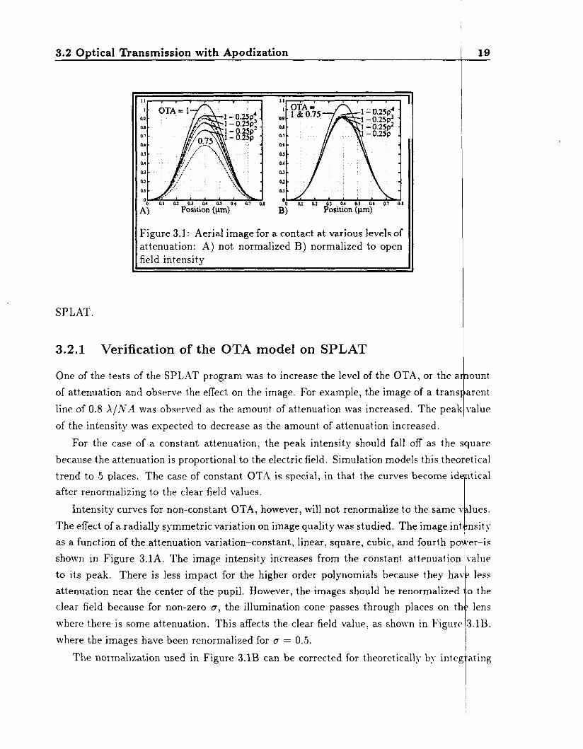
Figure 3.1 : Aerial image for a contact at various levels of attenuation: A) not normalized B) normalized to open field int,ensit,y
SPLAT.
3.2.1 Verification of the OTA model on SPLAT
One of the tests of the SPLAT program was to increase the level of the OTA, or the a
of attenuation and observe the effect on the image. For example, the image of a trans
line of 0.8 X / N A was observed as the amount of attenuation was increased. The peal of the intensity was expected to decrease as the amount of attenuation increased.
For the case of a constant attenuation, the peak intensity should fall off as the because the attenuation is proportional to the electric field. Simulation models this thec trend to 5 places. The case of constant OTA is special, in that the curves become id after renormalizing to the clear field values.
Intensity curves for non-constant OTA, however, will not renormalize to the same The effect of a radially symmetric variation on image quality was studied. The image in as a function of the attenuation variation-constant, linear, square, cubic, and fourth pc shown in Figure 3.1A. The image intensity increases from the constant attenuatior to its peak. There is less impact for the higher order polynomials because they ha attenuation near the center of the pupil. However, the images should be renormalized clear field because for non-zero Q, the illumination cone passes through places on tl where there is some attenuation. This affects the clear field value, as shown in F i g w where the images have been renormalized for u = 0.5.
The normalization used in Figure 3.1B can be corrected €or theoreticall>. b>. inte
19 -
.aunt irent
,value
pa re 'tical itical
lues. nsity er-i s
iral ue 1 less o the lens
3.1B.
at ing

20 Simulation of Non-uniformities in Sources and Optics in Projection
the OTA over the illumination cone, as described in Equation 3.1 which simplifies the last
expression for a radially symmetric source. When these integrals are carried out e actly. the results show that SPLAT is accurate to 3 places. f
Printing
3.2.2 OTA Effects on Image Quality
Several possibilities exist on how the attenuation will affect the image quality. It the values near the mask edges, values in the dark space, or values in the peaks. at the mask edge for a quadratic variation of 1 - 0 . 2 5 ~ ~ is shown in Figure 3.2A intensities as a function of feature size, in terms of X/NA, are plotted field). A variation in line edge intensity of only a few percent is present
The peak intensities for isolated transparent lines and contacts as
and non-attenuated cases.
with and without the same attenuation are shown in Figure 3.3. At very large feat re sizes. the intensities are all about the same. This is to be expected since the middle of t le lens is used for large feature sizes. At intermediate feature sizes, less overshoot is obser red. The i

3.3 Arbitrarv Illumination Sources
The source is represented by a rectangular grid composed of many pixels. The source first defined using geometric primitives such as circles, rectangles, and general polygon!; Figure 3.5). Arbitrary intensit,y weights can be assigned to the primitij-es to construct, example, a source with a radial variation in brightness. A table lookup approach of t h e is then used during the integration of the transmission cross-coefficients in Hopkins' of partially coherent imaging [Hop53].
' 0 0.1 0.2 0.3 0.4 0.5 0.6 0.7 0.8 0.9 1 1 1 1.2 1.3 1.4 1.5 1.6
ANA
is
(See for
source
theor!.
Figure 3.3: Feature size dependent OTA effects for isol- ated transparent lines and contacts
absolute decrease is more for the contact, making the line and contact images more s However, in the small feature size region between 0.5 and 0.8 1/NA where much litho] is done, both the line and contact intensities are about 10% lower. As a result, to 01 certain intensity, 75% of the clear field for example, features must be oversized. At th intensity level, the lines have to be oversized about 9% and the contacts have to be OVI
about 7%.
The effect on opposite polarity features is shown in Figure 3.4. M'hile the absolute i r in absolute intensity is small, the percentage increase is similar to the case above. F polarity, an intensity below 15% is desirable which would require a bias of about 8%.
3.3 Arbitrary Illumination Sources
21
rnilar.
raphy tain a ; 75% rsized
:rease r this
3.3.1 Operation and Implementation

22 Simulation of Non-uniformities in Sources and Optics in Projection
Figure 3.4: Feature size dependent OTA effects for isol- at.ed opaque lines and contacts
SPLAT also supports reading intensity matrices on top of which arbitrary s be placed. This is similar to placing transmission apertures into a system wit1
illumination variations across the pupil. Another possibility, no yet implemented to describe the illumination variation with an analytical function. An example inp with a radially distribution is shown in Figure 3.6. After placing a circular aperat = 0.6 the source appears as shown in Figure 3.7 and Figure 3.8.
A test of the program was to run it with a normal circular source and a a s o u m by a uniform intensity matrix with the same sigma. Figure 3.9 shows this coml CT = 0.6. The results differ slightly owing to the fact, that the discretized so1
larger source area and not a perfectly circular shape. When the grid density is
negligible differences are seen. A second test of the code was to examine the focu of a non-uniform distribution. Figure 3.10 shows intensity curves at several levels for a linear varying source and for a line perpendicular to the intensity variation. intensity values shift slightly to the left due to the asymmetric illumination. 'I observed for lines which are parallel to the intensity variation. A third test of thl to check the open field intensity values for the various sources and they all were wi
1 . 0 0 ~ range.
The way in which the integration was implemented is shown in Figure 3.1 1. P integration routines, used for the circular sources, were modified to sample the s(
Printing
iapes can
a known would be t contour re with cr
described srison for rce has a increased beha\.ior
If defocus The peak
i s is not code was
hin in tlic
-esi st ing e /Irce

3.3 Arbitrary Illumination Sources
Figure 3.5: Various geometric primitives
23
b
C
Figure 3.6: Contour plot of input intensity matrix with a radially distribution

24 Simulation of Non-uniformities in Sources and ODtics in Proiection
0 X
Figure 3.7: Illumination Source II
Printing

3.3 Arbitrary Illumination Sources
h Y v) .I
5 Y
U C
Y X
25
1
-P -1
m
11 Figure 3.8: Illumination Source for Radial Distribut,ion 11
Position (urn)
Figure 3.9: Comparison of Discretized Source With Uni- form Distribution and Normal Source

26 Simulation of Non-uniformities in Sources and Optics in Proiection
The interplay of source shape and feature orientation for periodic lines is illustrattrd ure 3.12 for a quadrapole illumination source. One of the ideas of this type of source there is an interplay between the angles in which the source drives the mask and in which the diffracted orders come off. A lot of energy can be put into the rays the left and right side of the lens to get a very low dependence on focus. For the and mask in Fig. 6A, an image can still print defocussed to 1.5 R.U. while mos'
- 0.OR.U. Delaw
0.5 R.U. Ddau
1.0R.U.Defau
1.5R.U.Mani
----. -......... -.-._
Position (urn)
in Fig- is that
the angles gcing down
source shape steppers
Figure 3.10: Linear Intensity Distribution: Imaging Thru Focus
only print up to about 1 R.U. Rotating the source by 45 degrees, or rotating tl-e 45 degrees, as in Fig. 6B, shows that the source orientation is important in that behavior with focus is deteriorated. At a defocus level of 1.5 R.U., t he pattern is
in the dark areas.
map. This approach facilitated the implementation and avoided writing complicate tion routines to determine the integration area. The trade-off, however, is an incrc simulation time, especially when a large number of pixels are used because ever)' pi be sampled to guarantee accuracy. Testing of the arbitrary source imaging with S ing circular sources is in agreement with those obtained with the source being rc analytically.
line b!, the good o\'er 2O(X,
Printing
1 intersec- ase in the tel should ?L.4T US-
presented
3.3.2 Effect of Source Shape on Image Quality

3.3 Arbitrary Illumination Sources
Region of Integration -, n of the
3gure 3.1 1: Implementation of arbitrary source illumin- ition
@ I
0 9
0.8
.g 07 06
05
$ 0 4
(d 03
9
.- Y
c( 3 0.2
0.1
0 0354 0.707 I .M I 1
Position ( m A )
Figure 3.12: Quadrapole illumination: Feature orient,at,ion effect,s for periodic li (kl=0.707). Source in A) is rot,at,ed by 45 degrees in B).
28 Simulation of Non-uniformities in Sources and Optics in Projection I Printinn
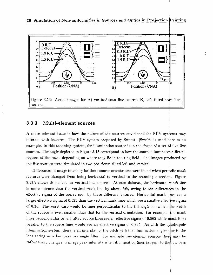
A more relevant issue is how the nature of the sources envisioned for EUV s
interact with features. The EUV system proposed by Sweatt [Swe93] is use example. In this scanning system, the illumination source is in the shape of a s
sources. The angle depicted in Figure 3.13 correspond to how the source illumi regions of the mask depending on where they lie in the ring-field. The image the five sources were simulated in two positions: tilted left and vertical.
Differences in image intensity for these source orientations were found when features were changed from being horizontal to vertical to the scanning dir 3.13A shows this effect for vertical line sources. At zero defocus, the horiz is more intense than the vertical mask line by about 5%, owing to the di effective sigma of the source seen by these different features. Horizontal larger effective sigma of 0.525 than the vertical mask lines which see a small of 0.35. The worst case would be lines perpendicular to the tilt angle for of the source is even smaller than that for the vertical orientation. For e lines perpendicular to left tilted source lines see an effective sigma of 0.56 parallel to the source lines would see an effective sigma of 0.325. As wi
illumination system, there is an interplay of the pitch with the illuminatio lens acting as a low pass ray angle filter. For multiple line element so
rather sharp changes in image peak intensity when illumination lines tan

3.4 Conclusion 1 29
filter circle move inside or outside the acceptance circle of the lens. With defocus the horizontal line images become non-symmetric, and intersect the
line images. The horizontal line patterns become asymmetrical with defocus due interplay of the asymmetrical source with defocus. Figure 3.13B shows the same
for the left-tilted source line which would correspond to the edge of the mask. The in the images are noticeably less, as the difference in effective sigmas are less.
vertical to the
simi.lation diffe:ences
3.4 Conclusion
SPLAT (version 5.0) can now simulate arbitrary illumination sources and wavefront ation. M’avefront attenuation reduces the intensity, and even with renormalization for, fields, small features require an approximate 8% oversizing with an OTA of 1 - 0.25prf. OTA can be implemented with only a 15% increase in CPU time through the use of variations. The shape of the illumination source does not have a major effect on the quality. Differences on the order of 5% are produced by the different scanning used in the bow-tie source. Reducing the discretization errors in arbitrary sources madc small elements increases the simulation time by an order of magnitude. Expressing the with analytical functions would definitely decrease this time. However, this would r completely rewriting the integration routines.
attenu- open The
ar..alytic image
positions from
shapes .quire

Bibliography
[Hop531 H.H. Hopkins. On the diffraction theory of optical images. In Proc. Roya 217, number 1131 in A, pages 408-432, 1953.
Derek C. Lee and Andrew R. Neureuther. Euv (soft x-ray) image simi projection printing. In OSA Proceedings in Soft X - R a y Projection Lz volume 18, Mont,erey, CA, 10-12 May 1993.
[LN93]
S O C . VOl.
lation for
h OSraPh Y 3
[Swe93] M’illiam C. Sweatt. High-efficiency condenser design for illuminating a rin OSA Proceedings in Soft X-Ray Projection Lithography, volume 18, 1993.

Chapter 4
MEMS Process Simulation using SIM
Ab st ract This project demonstrates the use of SIMPL System 6 to simulate MEMS (RlicroElectrohilechanical Systems) process flows by combining mask layout data with process flow information. SIMPL-2 (Simulation of Profiles from the Layout) and SIRIPL-DIX (Design Interface X-Windows) make up the core of SIhlPL System 6 and were the primary tools. The focus has been on developing SIRlPL System 6 to assist in the development of MEMS circuits and as a vehicle to coordinate process development with device design in a joint project on hlERlS with Analog Devices. As a result, SIhlPL System 6 has become much more functional and robust in regards to its internal algorithms and user interface. This project illustrates the success of using SIRlPL on the following R/IEIIS processes: RlICS process, Side Wall Beam process, Analog Devices ADNL5O process, hletal Beam process, and iRIEMS process. Various MEMS process problems are simulated and compared t,o lab results. A test mask for calibrating simulators and identifying some process problems has also been initiated.
4.1 Introduction
4.1.1 Motivation for Simulation
The technology understJanding and quantative analysis available in process simulat greatly aid the process integration activity. They can help identify t,echnolog!. issues severity of planarity, transition topographies, and device protection schemes. The\. IT help predict device failure mechanisms or process limitations. In addition the!, ma!. 1 to help assess the influence of deposition technology on device performance, or the E
process variations including misalignment errors.
Many processing issues exist in MEMS (MicroElectroMechanical System) proces
>L
s can ich as y also used
ect of
's. es-

32 MEMS Process Simulation usind SIMPL 1
pecially when integrating them with a standard device process. Due to the larg stack height in the fabrication of the mechanical structures, problems in ing, and deposition arise. A few examples are: resist thickness variations
variations, step coverage problems in deposition, and less predictable
flexure members due to process dependent effects.
4.1.2 Project Overview
This research has focused on developing SIMPL System 6 (generally referred t and using it to assist in the development of MEMS circuits. SIMPL (SIMulati from the Layout) has been used to visualize cross section evolution in severa cesses by combining mask layout data with process flow information. The int SMPL as a vehicle to coordinate process development with device design in on RlEhlS with Analog Devices.
The focus of research now even shifted to developing the tools rather th on more real lab examples as initially intended owing to the nature of the pr RlEhlS and the need to face up to algorithm limitations to achieve robustness. changes have been made to the both the internal algorithms and user inter effort. the capabilities of SIhlPL have improved significantly. especially in et and in the visualization of mask layers and cross-sections. Extremely co process flow have been simulated from start to finish, the largest of w 150 (SIRlPL) process steps and 22 masks. A number of of the cross addressing processing problems will be used to illustrate the current SUC
newly released SIMPL System 6. This chapter will begin with an overview of SIRlPL System 6 which w
to the subsequent section describing various process technologies as si In this section, comparison to actual lab results and investigation into will be discussed. The next section is similar, and will describe the u structures to identify processing problems. Finally, this is followed by future work and the conclusion.
4.2 Overview of SIMPL System 6
SIhlPL System 6 is a collection of software tools to simulate 2D device process'ng. The principle components of SIMPL System 6 are SIMPL-2 [IiLNsS] and SIhIPL-DIS [\\'+$$I.
SIMPL-2 contains most of the routines necessary for manipulating data and g nerat iiig I
4.3 Simulation of MEMS Process Flows
cross-sections. I t also contains first-order models for certain basic process steps: exp development, deposition, etching, implantation, diffusion and oxidation. These mod(
goal-oriented in nature, requiring input parameters which describe the dimensions and of the affected material after that step is performed. For example, implantations a proximated by a Gaussian function with a user-defined peak depth and standard devi
Deposition models require a material name and thickness to extended the current topog SIMPL-DIX (Design Interface in X-Windows) provides the graphics and user-int
capabilities of SIMPL System 6. A layout and profile viewer is provided along with a c
of design tools. All these features are thoroughly detailed in the SIMPL System 6 Guide [Ele95]. The release notes present in this document lists new features whid been developed in the effort to simulate the MEhlS process flows.
[W0+80] for physical deposition, isotropic and anisotropic etching of multiple non-planar layers, and optical graphy on a planar substrate. SAhJPLE deposition and etching has been used extensi! this project. Links to various other tools (e.g. SUPREhl [CHD83], [MELD881 for im ations) exist but will not be discussed as they were not used in this project. Again. refer to the SIMPL System 6 Users’ Guide for more information.
SIhlPL System 6 is also linked to SAMPLE [WOO791
SIhlPL utilizes the layout and process flow specifications to visualize the evolution del-ice cross sections. This has proven useful for designing complicated processes with more masks than a standard CMOS process.
4.3 Sirnulation of MEMS Process Flows
4.3.1 Overview of Simulation Cases
Several process flows have been created for simulation with SIMPL, and are listed in Tab Each will be covered in detail except for the proprietary AD1 M E M S process. The res( example will be used to illustrate the various etching models available. The NiYell C example will show the the overall MICS process-electronic devices with microstructure: position sensor example will show a stringer problem. The actuator example will shc use of SOG to remove the formation of stringers. The side wall beam technolog), ex will show the use of stringers to form hollow beams. The ADXL50 process is used to trate a more complicated example and the use of SAMPLE non-planar etching. The beam process will show the ability for SAMPLE to model resist flow. The .4DI Bihl fabrication test structures were designed to investigate processing problems in the fabri
of the ADML50 accelerometer and the multitude of structures designed at l iC Berkel
33 -
sure, 3 are
hape : ap- tion.
LPhY. rface riety sers’ have
apor it ho- ly in lant- ease
f the nan!.
84.3.1. iator b!OS The
- the
nple Ilus- ietal
IS2C i t ion
,’ (as

34 MEMS Process Simulation using
Process MICS
Side Wall Beam AD1 BihlOS2C hletal Beam AD1 BiMOS2C
part of the ARPA MEMS project).
Many other less complicated process flows (e.g. CMOS and NMOS) also exist included with the basic SIMPL System 6 software package.
Layout Purpose/Description Resonator Demonstrate Etching Model NWell CMOS Demonstrate MEMS Integri Position Sensor Stringer Problem Example Actuator SOG Planarization Examplc Beam Stringer Example ADXL50 Accelerometer MEMS Integration, Non-pla Sense Capacitor Resist Flow Example Fabrication Test Structures Fabrication Problem Detect
le micro- 3n added
ical con-
- layer of
The use khnolog). epos i t ed ributioii. 1 hospllo-
aft cr t h c
4.3.2 MICS
Process Overview
The hlOS fabrication process has been integrated with surface micromachining (
icon structures. The technique used at the University of California Berkeley is E
approach m.herebj. the ChlOS transistors are completely fabricated before any of t. micromachining [M'YHSO]. Hence the process is called the Modular Integration with microStructures, or RIIICS. The baseline process IC process is a 3pm design rul
poly. single metal ChlOS process. The standard aluminum metalization has beer with tungsten since aluminum can not withstand the high temperature annealing o f '
structure. A Tz,'V/TzSiZ diffusion barrier at the metal/silicon contacts has also bt to prevent the reaction of tungsten and silicon at 6000 C.
Surface micromachining is employed to add three levels of polysilicon. Elect nection between the micro structures and CMOS is accomplished through a jumpc polysilicon to prevent out diffusion of tungsten into the polysilicon deposition tubes of tungsten and its silicides has been borrowed from already mature VLSI process t and shows promise for increasing levels of integration. To minimize the stress in films, rapid thermal annealing (RTA) is employed to limit excessive dopant redis In addition, the structural polysilicon layers are sandwiched in between two doped silicat,e glass (PSG) layers so that t,he stress gradient in the polysilicon is minimized RTA .

4.3 Simulation of MEMS Process Flows
Simulation
35
more rigorously but this will not attempted as i t was not the main processing thrust.
defined below.
structural polysilicon layers.
Re sonat or

36 MEMS Process Simulation usini
r. I
Figure 4.1: Partial layout of a resonator showing a cut- line through an anchor and dimple
section using the most rigorous etching, referred to as SAMPLE-nonplanar etchin SAMPLE performs all the etching. In this case, the isotropic etching used t.o form t creates curved geometries as expected in a real process. For more details aboi
please refer to Appendix C.
MICS NWELL
The full view of a MICS cross section showing t,he N-well CMOS and sensor area i r Figure 4.5. In between the PMOS and NMOS transistors, there is a poly-pol). caI zoomed-in view of the the right side of the figure is shown in Figure 4.6. As describ
Figure 4.2: Cross sect.ion of a resonatlor showing dimple and anchor using primitive etching
SIMPL
; because Le dimple t et.ching
shown in 3cit.or. -4 d earlier.

4.3 Simulation of MEMS Process Flows
I I
Figure 4.4: Cross section of a resonator showing dimple and anchor using rigorous etching
37

38 MEMS Process Simulation usin
SELECT COmM I D
~ ~~~~
Figure 4.5: h4ICS full view before final release
electrical connect'ion from the sensor area is made via a polysilicon jumper layer
t,ungsten out-diffusion during polysilicon deposi t,ion. The jumper layer is more eas this figure.
Position Sensor
In etching the polysilicon beams, an etch is needed that is both highly anisot provides high selectivity of the poly with respect to the sacrificial oxide. However, in the structure, the anisotropic etch may leave poly residue unless a significant o
used. Unremoved poly can become a conduction path causing short circuits, or bin structures which should be free standing.
These types of problems were found on a particular position sensor design process, and they have been simulated. The cross-section shown in Figure 4.;
SIMPL
prevent
r seen in
'pic and sew h er e
r-etch is b.oget her
2 hllCS ias SP2

4.3 Simulation of MEMS Process Flows 39
Simulation of SOG planarization
A variation of the MICS process is to add a second structural lajeer. layer is desirable to serve as a limit stop for moving beams, upper ground planes. and
A second stru
stringer problems. The severity of the stringers has been exaggerated because the SP2 not over-etched, and subsequent isotropic etching was not done to help remove the process step included in the real lab process. The real device produced stringers ever. the normal precautions.
The main cause was the large step height (z1.4pm) under the stringer on the right. SXT mask is used to cut thru the CMOS passivation nitride and several underlying 1aj.ex-s to expose the gate polj’ (CPG) upon which SP1 is deposited to establish and connection. The solution was simply not to cut through the passivation with the SNT in areas under the SP2 shuttle area. The less severe stringer on the left of the figure is by many mask edges aligning (difficult to see from the figure) causing a more seyere The solution for this was to avoid aligning the SP1 mask edge to the CPG mask edge possible.
In this simulation, SAMPLE-nonplanar etching was used to perform the SNT cut. particularly useful because one etch step cuts through many layers of oxide: passivation (PSGP), CMOS oxide (PSGO), capacitor oxide (CAPO). Other methods of etching require the user to specify each layer of oxide to etch. Forgetting to etch through the layers would result in a step height of only about 0.6pm.
was stringers-a
with
The
oxide electrical
mask cwsed
step. when
It is oxide
ivould other

E 5 -6 E
.C
U c r
E C + 01
.C
c C
E .C
(/1 U U
L C
a
E: 5 s
0 1
r

4.3 Simulation of MEMS Process Flows 1 41 I
sense or actuation electrodes.
A problem with the earlier design of this process was the formation of stringers
(the second structural poly but the third poly in the backend MEMS process). A ation process employing the use of spin-on glass was used to solve this problem. The planarization process can now be simulated using SIMPL. In previous versions the
step did not work on complicated topography. An SEM cross section of the MICS 3-Poly process is shown in Figure 4.8 [Fed94:.
situation depicted is similar to but not the same as the one simulated by SIMPL. In this voids (complet,ely sealed from the top) were created between the fingers of SP2 duri:ig
c f SP3 planariz-
SOG etch-back
The case,
the
ends of the fingers. In essence, SP3 filled a tunnel. The lower SEM in Figure 4.9 [ deposition of PSG2. Subsequent deposition of SP3 filled these voids from openings
shows this situation. In contrast, the top SEM in Figure 4.9 shows the situation wh PSG2 did not completely pinch off. This is the what has been simulated using SIMPL first case requires 3D simulation and the representation of materials with holes which S was not designed to handle.
1 The SIhlPL simulation results of the second case are shown in Figures 4.10 and 4.
Figure 4.10 no planarization was used which resulted in SP3 stringers and undesirabl filling gaps between the SP2 beams. Again this situation has been exaggerated becai over-etch or extra isotropic etching has been done. Figure 4.11 shows the situation in the same etch times have been used but instead an SOG planarization step is added. the SOG filling in the gaps, no undesirable or residual SP3 is present.
4.3.3 Side Wall Beam Process
Process Overview
The Side IVall Beam Process [JH93] is a met,hod to fabricate hollow beams with a vel
resonant frequency for use in resonators. This process has been simulated using SI Simulating this process relies on anisotropic etching leaving behind stringers, which bl the beams, The process steps are listred below:
BASIC SIDE WALL BEAM PROCESS 1. D e p o s i t 4 urn p s g ( p s g 1)
2 . L i t h o g r a p h y - mask NP - forms mesas of o x i d e
3. P a r t i a l a n i s o t r o p i c e t c h of p s g ( p s g 1)- o n l y 2 urn of PSG 4 . S t r i p PR, c l e a n wafers
5 . D e p o s i t 0 . 2 urn p o l y s i l i c o n ( p o l y 1) & 0 . 2 urn psg (psg 2)
.t the ed93] e the , The MPL
1. In
b SP3 se no rhich LVith
\' low
LIPL. come

42 MEMS Process Simulation usin
I t
t
Figure 4.8: SEM cross section of MICS Poly-3 process
, SIMPL

4.3 Simulation of MEMS Process Flows 43
I ' * *
Figure 4.9: SEM top and side view of R4ICS Poly3 Process d
I

44 MEMS Process Simulation usin1
Figure 4.1 1: MICS Poly-3 Process utilizing SOC: planarization I
SIMPL

4.3 Simulation of MEMS Process Flows
Figure 4.12: Side wall beam mask -
6.
7. 0 .
9.
10.
11. 12. 13.
14. 15. 16. 17.
Lithography - mask NS - pattern poly (form sidewalls) Anisotropic etch of psg (psg 2)
Anisotropic etch of poly (poly 1) Deposit 0.2 um PSG (psg 3) Lithography - mask NPS - contact to poly 1 Anisotropic etch of psg (psg 3 and psg 2)
Deposit 2.0 um poly (poly 2)
Lithography - mask ND - poly 2
Anisotropic etch of poly (poly 2)
Lithography - mask NC - removal of stringers Isotropic etch of poly (poly 2) along sidewalls Isotropic etch of all psg layers
The initial attempts to simulat,e this process failed because simpl-2 could not han simulation of stringers. The et,ching algorithms had to be significantly ahered for this I to work.
Simulation Cross Sections
Several SIMPL cross sections are shown in Figures 4.13- 4.15 and the mask is shc Figure 4.12.
The various cross sections views demonstrate the non-trivial aspeck of this p SIRfPL can greatly aid in the visualization and process design, especially when t f can see the step-by-step process graphically on the computer screen.
45 -
the )cess
'n in
cess . user

46 MEMS Process Simulation usinj
Figure 4.13: Cross section through beam
Figure 4.14: Cross sect,ion through anchor I1
Figure 4.15: Cross section through anchor and beam 11
SIMPL

4.3 Simulation of MEMS Process Flows I 47
Process Overview
A technology to integrate a single-level polysilicon surface micromachined layer with a process was developed at Analog Devices [TACS93]. It is used to fabricated the fully integrated surface micromachined accelerometer used to deploy air bags in cars.
The ADXL50 process is an example of a process in which the micromechanici.1 electronics fabrication steps are intertwined. This 24-volt process provides considerable cuit design flexibility by providing vertical npns, substrate pnps, lateral pnpn, enhancement PMOS and NMOS, native NMOS, and trimmable thin-film resistors. The connection sensor with t,he electronics is achieved with n+ underpasses in the sensor area-no
tion is used for that purpose. Relatively deep junctions are allowed in this BiCMOS which permit additional thermal processing for the sensor material anneals as well as brief dielectrics densifications without severe device performance degradation.
4.3.4 BiMOS Technology
BiMOS AIlXL50
and cir-
of the mekaliza-
p-ocess other
In collaboration with Joe Kung at Analog Devices, the ADXL50 process was One of the initial limitations was the restriction of etching only six non-planar layers. described in Appendix C the top layers of the profile are exported to SAhlPLE for the planar etching simulation. This was extended to total of 20 layers, enough to satis:'>. ,4DSL50 process.
Figure 4.16 shows the cross section, test mask, and cutline of the ADXL50 process the main release etch. The SAMPLE-nonplanar capabilities are shown in Figures 4.17, and 4.19, each showing successive etch times. Special care must be taken to protect the of the del-ice during this long release etch. SIMPL can help reveal the effect of etching of these layers.
The success of the ADXLSO technology and the awareness of the benefits of levels of integration resulted in the ARPA zMEMS project involving Analog Devices ar Berkeley Sensor & Actuator Center. The goal of this ongoing project is to integrate with micromechanics which has not yet been realized. This would ext,end the number of sistors integrated with microstructures from the current number in the thousands inio hundreds of thousands [P+95]. It is hoped that the devices fabricated with this will have orders-of-magnitude improvement in performance over designs using single elements. The iMEMS approach is to create systems using many simple and imprecise ments. The performance is gained through averaging, matching, and ratiometric techn.
Simulation Cross Sections
deve.oped. -4s
non- the
-)efore 1.11. rest
on all
increased d the \'LSI tran-
the techrology
sense
ele-
qucs.

48 MEMS Process Simulation usin1
RETURN 6lUORT MODF SIWL I
Figure 4.16: ADXL50 before release etch *
Figure 4.17: ADXL50 after 160s of etching
II Figure 4.18: ADXL50 after 240s of et.chinp II
SIMPL

4.3 Simulation of MEMS Process Flows
t I .
I Figure 4.19: ADXL50 after 500s of etching I to reduce noise for example. Target applications include monolithic high-performance
axis acceleromet,ers, vibratory rate gyroscopes, mechanical filters, among others.
4.3.5 Metal Beam Process
Process Overview
In this unconventional process, the sacrificial layer is resist and the beam layers are Aluminum is used for the capacitor p1at.e~ because its low resistance was required to g
necessary capacitance sensi tivi ty.
SIMPL Simulation
The spinning of resist, in the old version of SIMPL, was not suited to simulate this 1 because the top surface of the resist also ended up perfectly flat, no matter what thl graphg was. Because the beam layer is deposited over the resist, the resist influer
shape. Real resist spun onto a wafer would exhibit thinning at step edges.
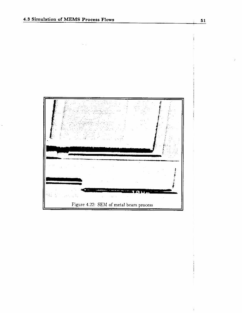
To model this effect to first order, the top profile of SIMPL was convoluted with a Gi function with an optional sigma. This was accomplished by placing the top surfac uniform grid, taking the discrete Fourier transform, multiplying it by the Gaussiar and then taking the inverse Fourier transform. A specified z-amount is also specified simulation results are shown in Figure 4.20 as compared to a SIMPL simulation in Figu without modeling any type of resist flow. An actual SEM showing a similar scenario u metal beam crossing over a trench is shown in Figure 4.22. The effects of resist spinn evident by the dip in the metal beam as it cross over tJhe trench. Also at the contact the metal layer slopes down.
At present this new deposition model only works for periodic structures in wh left and right side of the topography are similar. This could be changed b\r chang
boundary conditions to mirror each boundary.
49 -
mlti-
ietal.
n the
)cess opo-
's its
ssian on a
ilter, some 4.21. h the
g are
dges,
I the 5 the

50 MEMS Process Simulation usin
Figure 4.20: Simulation modeline: effects of resist flow
11 Figure 4.21: Simulation without modeline effects of resist flow
; SIMPL
4.3 Simulation of MEMS Process Flows
7
Figure 4.22: SEhl of metal beam process
51

52 MEMS Process Simulation usin
Anchor
Figure 4.23: Micromachined angular accelerometer: SEMs of the polysilic capacitors
Dimples
' I
in
I Residue 1
Process issues were investigated from the Berkeley dies of the first stage BiChl (Analog Devices ADXL50 process). Residue between the fingers of an angular were reported at the dimple locations. Initial investigation revealed that likely polysilicon and was caused a as a result of resist not clearing the etching of the polysilicon while defining the fingers. SEMs of this Figure 4.23 [Bro94].
A variety of test structures, shown in Figure 4.24, have been designed to isolate most likely causes of the residue and are all believed to be lithography related. causes may be due to the following: differences in resist thicknesses resulting
not clearing completely and impeding the polysilicon etching, reflection from
4.4.2 Test Structure Layout

4.4 Fabrication Test Structures
shoulders of bump areas causing standing wave nulls in the resist, and properties of maker when defining non-Manhattan lines.
The test structures on the bottom half of the figure (forming a semi-circle) are periodic lines and spaces of polysilicon (the beam layer) reproduced every 22.5', w also at 11.25'. The line/space ratios along a radial line starting from the center a 1:1, 1:2, and 1:3 with the lines always 4.0 p m wide. The test structures have b at various angles to test the mask makers ability to define non-Manhattan lines. line/space ratios will determine the effect of printing isolated and periodic lines. test structures in the center are 4.0 p m lines rotated every 11.25' with a 4.0 p m ring. This will test the residue problem at various angles. The other spoked t on the left of the figure is similar but the beam spokes are seperated every 22. structure between the spoked test structures consists of concentric rings of th seperated by 0.9, 1.0, 1.1, and 2.0 pm gaps. This will again test the rotational and the effect of etching the beam layer out of different size gaps without the p dimple layer.
The remaining test structures located on the top center of the figure are s
detail in Figure 4.26. The test structures are made of an inner disk of polysi by an outer ring of polysilicon. The gap between them increases from left to if the residue is dependent on etching. The gaps are circular to test the angul of the mask maker, and the bump mask width increases from top to botto dependence of resist thickness variations.
4.4.3 Simulation
53
Simulation with SIXlPL using the lithography capabilities of SAMPLE indicates that the case of resist not clearing due to resist thickness variations is feasible. The simulation are shown in Figure 4.25. Cutline A-A' cuts thru a region with a resist thickness of
while cutline B-B' cuts thru a region with a larger resist thickness of 1.5 p m because bump etch removing 0.5 pm of oxide. If the lithography is optimized to develop resist thick, openings in thicker resist will not be as large and may not clear in some cases. problem can usually avoided if a longer development times are used or if the resist are decreased by spinning on an overall thicker resist coat.
Unfortunately, at the time of this writing the die were not returned in time for exami:iation so the results can not be reported at this time.
A computer program was created to generate the test structures described above input is a file containing commands and coordinates and the output is a CIF file
first results 1.0 pm
of the 1.0 pm
This diffe~ences
The conti.ining

54 MEMS Process Simulation usin1
Figure 4.24: zMEMS Fabrication test structures
SIMPL

4.4 Fab r kat i on Test S t ruc tu res
It n
ll Goss Section A-A’ BUMP
Goa Section B-B’
R S l n
Poly
Oxide
S1hcon
I1 Figure 4.25: Lithography simulation with SIMPL
55

56 MEMS Process Simulation usin4
II B B E A M S H B U M P S H A N C H II I Figure 4.26: MEMS Circular fabrication test structures
SIMPL
4.5 Future Work
CIF polygons. Simple geometry can be entered to create objects which can be copied rotated by any angle. Future test structures can now be created with less difficulty. of commands available can be found in Appendix D.
I 57 -
and A list
4.5 Future Work
Though SIMPL has existed for many years, it needs to continue to evolve to keep the technology and its applications. The user interface is somewhat outdated and improved. Now that many more mask levels are being simulated, a more convenie viewing them with the layout editor is required. This has been alleviated by all0 to be outlined or hidden, but overlapping color schemes are also desirable and simulation results easier to interpret.
Integration with other process simulators also needs improvement. The link to
needs does not work well for large cross sections requiring large dopant meshes due limitations. Other useful features of SUPREhl, such as diffusion with oxidation, ar
Currently only diffusion can be done in an inert environment. Lithography simu the link SAMPLE is limited to planar topographies. More rigorous lithography could be possible with a link to TEMPEST [Uron94], a 3D electromagnetic simula this may not always be practical depending on the computing resources available.
Other problems continue to persist, such as the robustness of the etching and routines. Though they have greatly improved, cases exist where they may fail. problems also exist such as the capability to implant thru material other than users will find that normal processes will work fine but may run into trouble something more exotic.
A limited amount of work in the lab has been performed for comparison with S type of work would be useful for calibration and verification of the deposition models. New models could be developed and added to the simulator where the e are inadequate.
Lastly, this work has been limited to 2-D simulation. Key process flow ste
would benefit from 3-D simulation to examine critical MEM features in detai now that the SAMPLESD code has matured and become more stable. Possi are the the release of structures, and the formation of the end features on
which contribute to fringe field effects. Exporting the resulting topographies t and electrical analysis tools is also now a possibility from the recently added S.4MPLE to FastCap [SN95] for interconnect analysis.

58 MEMS Process Simulation usin
4.6 Conclusion
SIMPL has proven to be a very useful tool for studying the complex interrelatioi
goes into the fabrication of MEMS devices. Many MEMS related applications successfully simulated (See Table 4.3.1) and have provided insight into the fabricatic It is hoped that with the new capabilities and increased robustness, SIMPL will b as a working tool and establish a large user base. The user guide is quite completc lot of useful information as to get the most from of the existing code. Nevertheles will continue to evolve, as it did in my hands, as well as in the hands of the others
SIMPL
hips that ave been . process. accepted tnd has a the code efore me.
Bibliography
-1453,
S1.S-
[Bro94]
[CHDS3]
RI. 14’. Judy and R. T. Howe. Polysilicon hollow beam lateral resonators. In Nicro Electro A4echunical System M’orkshop, Ft. Lauderdale Florida, 1993.
Y. Sakai E;. Lee and A.R. Neureuther. Topography-dependent electrical meter simulation for vlsi design. In IEEE Trans. Electron Devices, volume ED, pages 1469-1474, November 1983.
[Ele95]
IEEE Februar!?
para- 30 of
[Fed941
[JH93]
[hlELDSS] C. S. Rafferty M. E. Law and R. \4’. Dutton. SUPREM-11,’ Users Afunual.
[I.; LN S3]
19S8.
Tim Brosnihan. Sems of angular accelerometer from adi bimos2c process
S.E. Hansen C.P. Ho, J.D. Plummer and R.W. Dutton. Vlsi process mc Suprem-iii. In IEEE Trans. Electron Dew., number 11 in ED-30, pages 143€ November 1983.
Electronics Research Laboratory, University of California, Berkeley. SIMP TEA9 6 b‘ser Guide, February 1995.
Gary Fedder. Sem cross section of mics poly3 process, 1994.
[P+95] R. S. Payne et al. Surface micromachining: from vision to reality to yisicn. IEEE Int. Solid-state Czrcuits Conf., San Francisco, Calif., 1995.
John F. Sefler and Andrew R. Neureuther. Extracting solid conductors single triangulated surface representation for interconnect analysis. In IEEE 1995. Get rest of reference from John!
W. E;. Tsang T. A . Core and S. J . Sherman. integrated surface-micromachined sensor. In Solid Stale Technology. pages 40,42,44,46-47, Oct,ober 1993.
[SN95]
[TACS93] Fabrication technolog!.
In
f:om a
. . ..
f x an 39-

60 BIBLIOG
[W+88]
[W0+80]
[Won 941
[ IVO 0 791
[IVY H 901
H. C. Wu et al. Simulated profiles from the layout, design interface in dix). In IEDM Technical Digest, December 1988.
A.R. Neureuther W.G. Oldham et al. A general simulator for vlsi lii and etching processes: Part ii - application to deposition and etching. Trans. Electron Den, number 8 in ED-27, pages 1455-1459, August 15
A. Wong. Rigorous Three-Dimensional Time-Domain Finite-Diflerc tromagnetic Simulation. PhD dissertation, University of California, Department of Electrical Engineering & Computer Sciences, Septem
(Memo No UCB/ERL M94/69).
A.R. Neureuther W.G. Oldham, S.N. Nandgaonkar and M.M. O’Tooll era1 simulator for vlsi lithography and etching processes: Part i - appl projection lithography. In IEEE Trans. Electron Dev., number 4 in ED- ’ili-722, April 1979.
M’. C. Tang I&’. Yun and R. T. Howe. Fabrication Technologies for Microdynamic Sysfems, pages 297-312. Elsevier Science, Amsterdam.
LAPHY
c (simpl-
iography In IEEE io.
,ce Elec- Berkeley, ier 1994.
. A gen- cation to
!6. pages
n t egra f ed
990.
Chapter 5
Conclusion
The simulation programs SPLAT and SIMPL System 6 have been successfully utilize( simulation of EUV projection lithography and the fabrication of MEMS devices respe Through this effort, new functionality and robustness has been added to both progra
SPL.4T was applied to several image quality studies taking into account the fo characteristics of prototype EUV systems: highly aberrated optics, non-uniformities illumination. and non-uniform source geometries. The extensions made to SPLAT ir representing aberrations across the pupil with Zernike polynomials and wavefront n
more accurately model a real system. The image quality studies using a rotating un source model showed that source spot to source spot image displacement rather thar
degradation for a given source spot location currently limits the resolution. SPLAT M extended to simulate arbitrary illumination sources and wavefront attenuation. \I’a attenuation reduced the printability of small features require oversizing dependent level of attenuation. The shape of the illumination source proved not to ha1.e a majo on the image quality.
SIhlPL has proven to be a very useful tool for studying the complex interrelatic that goes into the fabrication of MEMS devices. Utilizing layout and process flow infor SIhlPL was successfully used to visualize the cross evolution in the following processes: process, Side Wall Beam process, Analog Devices ADXL50 process, Metal Beam pi
and zhIEhlS process. Various MEMS process problems were simulated and compared results. This work was possible through the the new functionality and robustness progra into SIMPL System 6.
n the i vely. S .
wing n the luded ps to ilator mage j also
%front n the effect
ships ,at ion
rlICS )cess. o lab nmed

Appendix A
File Structure of SIMPL System 6
The directory file structure of SIhlPL System 6 is presented below. All nodes directories. The SIhlPL System 6 Users’ Guide can be found in S I M P L s Y S 6 / L
is the best source of information on getting started using SIMPL System 6. hl examples used in this report can be found in SIMPLSYS6/DEMOS/MEMS.
demo doc lib scripts src t,ut,orial
s i m pl s y s6 / s r c
samplel.8b simpl-2 simpl-dix utilit,ies Y
cdram cmos dram epi hunch litho mems nmos npn2 phase planar sdram trench
actuator adxl50 blade cmos-mics metalheam positionsensor process flows resonatl
.epresent K which
st of trhe
- . test s t ruct urc

Appendix B
page. 'L3' stands for Level 3 simulation in which S.4MPLEnonplanar etching and r SAMPLE deposition was used for most of the etching and deposition steps. The other flows used to generate the examples in this report are available with the standard System G software release. I
MICS Process Flow
,orous
'ocess [MPL

64 MICS Process Flow
I 1
3 4 5
6
7
8 9
10 11
12 13
14 15 16 I 7 18 19
20 21
12 13
24
25 26 27
28 19
30 31
32 33 34 35
36 37
38 39 4 0 4 1
I2 I 3 44
45 46
47
48
49
g ............................. I i i c s . L 3 p r o r o a r 8 F r o n t End b Back End process g ............................. I
I
8 Frent End B.rh1.y IICS Precess f l o w 8 R i c r e l a b cnos PIO~OII I Version 2 . 1 ( I a n . 4 . 1993) I 2 u i . I - m o l l . doublm poly-SI. singlo i o t a 1 I 8 r i i p l - 2 ot 'h ing used f o r III~ e t c h i n g s tops 8 I m p l a n t a t i m s R i r r i n g I
8 1 Initial Yet O x i d a t i o n ( 11 W l C I PROCESS * OIID OIIDE TIICKIESS l i ~ c r e - l ~ t o r ) * 0 1 De you wish t e us. d s f a u l t paruot*rs ( y o 1 or ne) ' yes DO YOU Y A I T TO ORAN TIE CROSS SECTIOI * yes
8 2 Yell Photo #ask YlICI PROCESS ' DEPO IARE OF THE RATERIAL ' RST THICKIFSS or THE nATmIAL h i c r o - n t o r ) 7 I oooooo VERT. SPII-01. ISO. AIISO SAIPLC REN ( 1 . s . i . ~ or n ) 7 s w TW WAIT TO DRAY TIE CROSS SECTIOI * y o 1
I I Y U L IASK YWICM PROCESS * urn WHICH RASK * CY1 IIVERT TIE IASK I p s o r ne1 ' p s IARE OP TWE IATERIAL TO DE EXPOSED ' RST IARE OF THE ElPOSW RESIST * U S T DO TW WAIT TO DRAY T I E CROSS SECT101 ' y o 1
w w m PROCESS * DEVL IARE OF T I E LATER TO BE DEVELOPED ' ERST DO TW WAIT TO DRAY T l E CRIES SECTIOI ).Os
8 3 Y.11 Implant
8 4 Moll D r i v e - I n ( t r x 35)
8 4 2 Etch p a t t e r n i n t o oxid. i n 5/1 D I P YlllCH PROCESS ' ETCR MWICW LATER DO TW WAIT TO ETCI * OKID ETCH ALL (yes er no1 * nr
51 DO TW MAIT TO DRAY T I E CROSS SECTIOI (yo$ or no) ' ybs 52 53 8 4 3 R * i s r o PR 5 4 YHlCI PROCESS ' ETCI 55 YHlCM LATER DO TOU WAIT TO ETCI * RST 56 ETCM ILL ( y e s or ne) ' yes
57 58 59
60
61
61 63 64
65
66 67
68
69 70
71 72 73
74 75 76 77 78
79
80
81 12 83 84
85 86
17 88
89
90
91
92 93 94 95 96
97 98 99
LOO 101 102
103 104
U
I 4" 5 Yel l Drivm In YllICR PROCESS ' O I l D OIIDE THICKIESS (ilcre-i*tor) * 0 300 Do you wish t i US. d-fault paruoterr I p s er n e ) ' yes DO TOU MAIT TO DRAY TlE CROSS SECT101 yes
I 5 0 Pad O x i d a t i o n / I i t r i d e D o p o s i t i o n
I 5 2 R . i o w a l l m i d o w c w PROCESS * ETCI wicn LATER DO TW WAIT TO ETCI * OIID ETCW ALL I p s or n o ) * yos DO TW WAIT TO DRAY Tnc CROSS s m m * p~
8 5 4 Dry O x i d a t i o n wcti PROCESS * OIID O I I D E TlIClIESS ( i i c r o n t o r l * 0 0300 00 you wish t o us. d o f a u l t p a r a m e t e r s I p s er ne1 ' )os DO 10U W A I T TO D U Y TWE CROSS SCCTIOI jor
I 5 5 I i t r i d o D o p o s i t i o n MWICW PIOCESS ' Depo IARE OP THE RATERIAL * ITRD TIICKIESS OF THE RAIERIAL (micro-m.tor) * 0 lo00 VERT. SPII-01. 150. AIISO or SAIPLE IWV (V.S.I.1. er I) * I DO TOU WAIT TO DRAY TIE CKOSS SUTIDI * ).os
I 6 0 Actiro Area P h e t o wnicw Pnoce5.s * expo wnIcw n i s i * CAI I IVERT TIE BAS1 I p s er ne1 * no IAUE OF TIE n i i u I u TO DE mmsw * mno I A l E OP TIE EXPOSED RESIST ' =ST DO TOU WAIT TO DRAY TIE CROSS SECT101 * yes
8 7 0 H t r i d a Etch YWICI PROCESS ' DEVL I A l E OF T I E LATER TO DE DEVELOPED ' US1 DO TW W I T TO DRAY T I E CROSS SECT101 * yes
8 8 . 0 . ?bid (P-) Implant Phete IRoworred I - Y e l l Iarkl YRICI PROCESS ? DEPO IARE OF TME RATERIAL * RST TWICKIESS OF THE IATCUIAL ( l i L I . - H C e I ) * 1.WWOO VERT. SPII-01. 150. 11150 or SARPLE R W V ( V . S . 1 . 1 . er I) ? 5 DO TW MAIT TO DRAY TIE CROSS s e c t m I 1.1
105 106 I I Y U L IASR IRoversod) 107 Y I I C W PROCESS EXPO 108 YWICR RASK ' CY1 109 IIVERT THE RASK I p s er no1 * I. I10 IARE OF' THE RATERIAL TO BE EIPOSED ? RST 111 #ARE OF TIE EIPOSED RESIST ERST 112 DO TW YAlT TO DRAY TWE CROSS SECTIOI ' yo1

MICS Process Flow 65
113 114 YIICI p a o c w * DEVL 115 IARE OF T I E L A l E R TO BE DEIELOPED ' ERST 116 DO IW WAIT TO DRAY TIE ClOSS SECTIOI * p a 117 118 8 9 0 r i e l d (P-I Ion implant 119 I20 8 10 0 Lscos Oxidat ion ( target 651 121 122 8 LO 1 Remere P I 123 wnicn PROCESS * cicn 124 v i m LAVER DO vw WAIT TO CTCR 7 RST 125 ETCR ALL (yes er ne) ' ye8
126 DO TOU WAIT TO DRAY T ie CROSS SECTIOI 7 yes 127 128 8 10 3 Yst o x i d a t i s n
130 OXIDE TRIClIESS (micre-8ot.r) ' 0 65
129 YRICR PROCESS ' OXID
131 0 s p U * I s h t * Use default p a r U S t O r l (yes e? no) ' 7 - S 132 133 134 8 11 0 Ii tride RemeVal
13s wnicm PROCCSS * EICR 136 wiicn LATER DO iw YAIT TO e m * ITRO 1 3 1 ETCI ALL ( p a ar ne1 * yos 138 139 140 8 I 1 0 S a c r i f i c i a l O i i d s
DO IOU YAIT TO DRAY TRC CROSS SECIIOI * yes
DO 1W WAIT TO DRAY IRE CWSS SECT101 ' yes
141 wnici PaocEss * CICII 142 wucn LAIU DO iw MAIT TO CTCU * o m 143 ETCl ALL ( p a or ne) ' ns 144 iimi or V'EIITICAL cTcn (micr*-mstsr) I 145 RATIO i f z or cTcnIma ( 0 o <- RATIO <- i 01 * o o 146 DO .IOU WAIT TO DRAY TIE CROSS SECTIOI (yes .r no) * yea 141 148 wnrcn PRWESS * OXID 149 OXIDE TIIClIeSS (micrenter ) * 0 0200
150 Do p u .Ish t o QS. d.fault p a r u e t e r s ( p a no) * yes 151 00 1W YAIT TO DRAY TUG CWSS SECTIOI * yes 152 IS3 8 13 0 I-Channel Ihr.sh.14 Implant (b lanket) 154 155 8 14 0 ?-Ch.nn*l l h r * s h s l d Implant P h s t e (Use t h e f i r s t maak I - Y e l l ) 156 wicn PROCESS * DWO 151 mine OP THE niiuiii * as1 158 T I I c l I E s s OP Tnc IATERIAL ( m i w i n t e r ) * I oOW00 159 VERT. SPII-01. ISO. AIISO S T s m L c IGN (v .s . I .A . or H I 7 s 160
161
DO IW WAIT TO DRAY TRE CROSS SECTIOI * yes
-~ 162 w n m PROCESS * EXPO 163 YRICI nisi * CUI 164 I i w a T rwe RISI (yes .r ne) 7 70s 165 IAl lE OF THE RATERIAL TO BE ElPOSED ' RST 166 I A R C OF THE EXPOSED RESIST ' ERST 161 00 1W WAIT TO DRAY T I E CROSS SECTIOI * p s 168
169 YnIcn p a o c e s s * OEVL 170 IAHE OF T I E L A l E R TO 0E DEVELOPED ' ERST 171 172 113 8 15 0 P-Channel T h r e s h o l d Implant (nark I-Iaak) 174
DO 1W Y A l T TO DRAY TRE CROSS SECTIOI ' ye8
115 Ynicn PRDCESS * ETCR 176 wnici L i m a DO IOU WAIT TO e m * UT
i n DO IOU WAIT TO DRAY Tnc CROSS SUTIOI * yes 177 ETCIl ALL (yea or n e ) * yes
179 180 8 16 0 Qat. Oiidatirn/Pely-Si D e p o s i t i e n 181
182 8 16 3 Dip e f f S a c r I f i c I a l ~ 1 1 6 s 183 184 8 16 4 Dry Oxidatien
186 OXIDE TIIClIESS ( m i c r o n t s r ) 0 050 181 Ds ysu . ish t e us* dsr.ult paruetors ( p a er ne) p a 188 189 190
ins wuicn PROCESS * OIID
DO VW WAIT TO DRAY TIC CROSS SECTIOl * yes
8 16 5 Oat. P e l y D.pwi t ion
192 IARE OP TRC RATERIAL * PLlQ 191 wnIci PROCESS 7 DWO
193 THIC~ICSS OF T i e n i T c n i i L (8iCrO-mStSr) * o 4s 194 VERT SPII-01. 150. IIISO er SAHPLG IuV (V .S .1 .1 , sr I) ' I 195 DO IOU MAIT TO DRAY T I C CROSS SECT101 (yes er ns) ? p a
197 8 17 o a.t* h f i n i t i s n a r e miv-cm
199 IARE or TnE IATWIAL 7 1 s t 200 TnIciicss OF TIC IATUIAL (micre-tsr) * i 201 VERT. SPII-01. ISO. AIISO sr s a m e n u u ( v . s . I . A . er I) * s 202 203
196
198 WiIcI PROCESS ' DWO
DO 1W Y A I T TO DRAY TIE CROSS SECT101 (yss sr ns) ' yes
204 YnIcn PROCESS * cim 20s YIICR n i s i * cw 206 IIVERT Tne IASI (yes er - 208 IAIIE OF Tne EXPOSED RLZIST * erst 20) DO IW Y A W TO DRAY Tne cwss SECIIOI (yes sr ne) * yes
211 w c n PROCESS * OEVL 212 IAEE 01 THE LAIU 10 BE DEVELOPED * ef8t 213 DO rw WAIT TO DRAY Tne CROSS SECTIOI (yes OT me) * p s 21, 215 8 I 8 0 Plasma E t c h poly-SI (PLIQ) 116 8 S t a r t i n g T h i c k n e s s - 0 45
20? IARE OF IlATERIIL TO BE ElPOSW r s t
210
zir 218 wwcn PROCESS * mcn 219 u m n LA^ DO iw u m e m * PLVO 220 ETCR ILL (yes er ne) * ne 221 A n m T 01 VERTICAL ETCI (micr.-=.teri * o 60 222 RATIO I I Z OF crcnina ( 0 o q- RATIO <- i 0 ) - o i 223
224 DO IW WAIT TO DRAY TllC CROSS SECTIOI ( p a *r n s ) ' yea

MICS Process Flow
215 226
227
228
229 230 231 232
233 234 235 236 237
238 239 240
24 I 141 243
244 245 246
247 248
219 250 251
252 253 254
255 256
257 258 259 260 261 261 263 264 265
266 261
261 269
270
zri 272
8 P I Strip
YIICI PROCESS * ETCH vnicn L i i m DO iw YIIT 10 ETCH * rst ETcI ILL (yes or ne1 * p s DO 1W WAIT TO DlAY TME CROSS SECTIOI (yes or n.1 * yes
8 19 0 Capaciter Permatien # Dry Oxidatien (SIIPL muat d.p.1it o x i d e )
8 19 3 Dry Oxidatim VMICI PROCESS ' DWO I A R E OF TIE lITERIIL ' CIPO rniciiess OP TIE IITERIIL (micre-m*tor) 7 08
VERT. SPII-01. ISO. AIISO 01 SAUPLE WEN (v.s.I.I. or R I 7 I DO 1W Y I I T TO D R I Y TIE CROSS SECTIOI (yes or no) ' 1.1
8 19 4 Oopstit Capacltw Poly YIICM PIOCESS ' DWO I I I E OF TIE IITERIIL * PLlC TllIClIESS OP TIE RATERIAL (mirr*-mot*r) * 45 VERT. SPII-01. Iso. AIISO or SIRPLE Iwu (V.s.1 A. or I1 I DO 1W Y11T TO DRIY TIE CROSS SECTIOI ( p a er no) * yes
e 20 0 Capacitw Phet. Iark
YIICI PROCESS ' DWO I A I E OF TIE UITERIAL * RST TIICIIESS Or TIE IATERIAL (mlrre-metor) * 1
VERT. SPII-01. ISO. AIISO er SAIPLE H E N (I 5.1 1. or I1 ' S
CIP POLl-CU
DO 1W YAIT TO DRAY TIE CROSS SECT101 ( Y O 0 or ne) * 1.8
YIICM PROCESS * ElW YlICB U A S I - C U IIlERT THE IASI (yes er no1 * no 1111 O? IITERIAL TO BE EXPOSED * IS1 I M E OF TIC EXPOSED RESIST * .rat w iw WAIT TO DRIY TIE CROSS sectron ( p a er no1 * 1 0 s
YIICI PROCESS DCVL WARE 01 TIE LAlER TO BE DEVUOPED * orst DO 1W Y I I T TO DRAY IRE CROSS SECTIOI (yes or no) * p s
21 0 ?la... etch capocltor polj-Si (PLlCl 0 Starting Thickness - 0 45 YBICI ?ROCESS 7 ETCH YIICM L A ~ E R DO iou YAIT ercm * m i c
281 282 283 284 185 286
287 288
289
290 291
292 293
294 295
296
291 298 299 300 301 302 303 304 305 306
307 308 30) 310 311 312 313 314 315 316 317 318 319 320 321 322 323
324 325
326
327 328
VIICH LIlER DO IOU YAIT TO ETCl ' rst ETCR ALL ( y e s or no1 ' p o DO 10U Y I I T TO DRAY THE CROSS SECTIOI ( p a or no1 * p a
# 22 0 I+ S/D Photo
8 23 0 I+ S/D Implant. Irsenic
8 24.0 I+ S/D Anneal
I 25.0 PI S/D Phata
I26.0 P* S/O Implant: Arsenic
8 27 D PSO Dopositien and D.nxiiicati.n
I 27.3 u m n Pnocess ? DM I I R E OP TIE RATERIAL ? PSOO TlICIIESS OF TIE IITERIIL (micrr-met.rI ? 0.7 1ERT. SPII-01. ISO. IIISO er SIIPLE I E N (V.S.1.A. er I) ? I SOURCE TlPE (U.D.I.C..r P I * I
Includ. Surface Rigratien (1 er I) ? 1 lIRIAICE I1 ITOlIC UOTIOI (a. ..E. 0.181) ? .OS W 1W WAIT TO DRIY TIE CROSS SECTIOI ( p a er nmj ? pi
sPuTTeiIia SOURCE AiaLE (d.gr..#. ..g. 45.01 ? 4s
2 8 . 0 . Contact Ph.t. Iaak YBICI ?ROCESS ' D E W I I I E OP THE RATERIAL * rst TIICIIESS OF T I C IIIERIAL (micr.-mt*r) ? 1 lERT. SPII-01. ISO. IIISO er 511PLE IUU (V.S.I.A. or I) ? S DO 1W M I I T TO D l I Y TIE CROSS SECTIOI ( p x st no) ? p r
YlICI PROCESS ? EXW YIICI IlSI ? CCI IIVERT TIE M I S 1 ( p a or ne1 7 y4r I I I E OF IATERIIL TO BE EXPOSED ? rat I A l E OP TUG EXPOSED RESIST * *rat DO l W YIlT IO DRAY TIE CROSS SECT101 ( p a mr n.1 ? p r
YIICB PROCESS ? DE11 IAIE OP TEE LAlEl TO BE DElUOlED ? orat W 1W WAIT TO D l I Y TRE CROSS SECT101 ( p x mr no1 ? pi
* 29.0: centact Etch (csao. CAW. and OXID1 YWICI PROCESS ? ETCH YWICl LAlER DO 1W Y I I T ETCI ? ?SO0
274 AIOUIT Or VERTICIL ETCH (micr.-m.t.rl * 0 60 275 RATIO X/Z OP EICIIIO ( 0 0 (- RATIO (- 1 01 ' 0 0 276 DO vw WIT TO DRAY TIE CROSS SECTIOI (7.1 w M I * 1.1 217
z m 0 PI strip 219
210 YRICI PROCESS * ETCR
330 331
332 333 334
335 336
AROUIT or VERTICIL ETCI (mirr.-m.t.r) ? 0 . 8
00 IOU WAIT TO DRAY TIE CROSS SECTIOI ( p s .I no) ? yon
YlICI PROCESS * ETCB YlICl LAlER DO 1W W I T ETCI 7 CAPO ETCR ALL ( y e s or ne) ? ne
RITIO I I Z OF eTciiia ( 0 . 0 c- RATIO <. 1.0) ? 0 .9

MICS Process Flow 67
337 330 339 340 341 341 343 344 345 346 347 340 349 350 351 352
353 354 355 356 357 358 359 360 361 361 363 364 365 366 361 368 369 370 371 372 373 374 375 376 377 378 379 3110 381 3117 30 3 3114 3115
A R ~ T OF VERTICAL cTcn (micr0-m.t.r) * o i RATIO I/?. OF ETCHIIG ( 0 0 <- RATIO <. 1 0 ) * 0 0
DO 1OU WAIT TO DRAY TIE CROSS SECTIOl (1.1 or no1 ' yes
u n m PROCESS * ercn w c i L a m DO TOU MAIT ETCH * OIID ETCH ALL (18: or ne) ' no
A R W I T OF VERTICAL ETCH (mlcr.-motor) ' 0 1 RATIO 117. OF ETCIIIO (0 0 <- RATIO <* 1 0 ) ' 0 0
DO IOU YAlT TO DRAY TRE CROSS SECTIOl (1.1 or no1 * yes
0 PI Strip
wicn PROCESS * arcn WnIcn LATER w iw W A ~ T TO w c n * rs t ETCR ALL (pi or no1 * yes
DO IOU YAlT TO DRAY TllE CROSS SECTIOl (18s Or ne) ' ,a:
I 30 0 Back rid. etch
31 TiS i l Forut1.n
0 31 Tun8st.n l . tal lIzat1.n
YnIa PROCESS * om IAUE OF Tnc n i r e m L * 11
VERT. SPII-ow. ISO. AIISO or s i m e nevu (v.s.I.A. n) * I TI1KCllESS O? TllE IATERIAL (mlcr.-metor) * 0 6
DO IOU Y A l T TO DRAY T l E CROSS SECTIOI (yes Or no) ' y e 1
* 33 R.ta1 ?hot. Mark
wucn PROCESS * ewo wnicn nisi 7 cn? IlIERT TllE UlSI (yo: *r no) * ne IIUE or nATenIu TO BE EIPOSW * ni I l l E OF THE EIPOSED RESIST * ors t DO IOU WAIT TO DRAY TllE CROSS SUTIOl ( 1 8 s er ne)
Tun8:t.n I Tlntanlum Etch
ye:
0 34
18b W111C1 DEVL 387 #ARE OF THE LATER TO DE DEIUOPED ' orrt 308 Do IOU YAlT TO DRAY THE CROSS SECTIOl (1.1 or ne1 ' p s 389 390 35 S i n t * r l n g and Test
392 36 Std Tun8st.n C l a m 391
393 394 395 396 397 390 399 400 401 402 403 404 405
406 407 400
409 410 411 412 413 414 415 116 417 411) 419 420 421 411 423 424 425 426 417 428 429 430 431 432 433 431 435 436 437 4311 439 440
37 - cnos PAssIvATIoa
wIcn PROCESS * DEPO WIE OF TnE nATER1iL I PSGP
VERT. SPII-on. ISO. AIISO or sinwe nwu (v.s.I.A. er I) ? I swam T i P e (u.D.n.c.er P I 7 n SWTTElIlG SOURCE AIGLE (dogre.:. e g. 45.01 ? 46 Includ. Surtac. Ri8ratie.n (1 sr #I ? 1 VAIIIAICE II AronIc ROTIOW CUB. 0.g. 0.1811 ? .os DO 1W YAlT TO DRAY THE CROSS SUTIOl (yo: or ne) ? p s
THICIIESS OF THE RATERIAL (mkre-mt8r) * . 4
w x c n PROCESS * DEPO
rnIcriess OF Tne n A m I A L (micro-uter) ? D.18 VERT. SPIN-om. ISO. m s o 8r s i m e IWU (i.s.1.1. or I) ? ISO DO IOU u m TO DRAY rnc CROSS SUTIOI (yes er ne) ? yes
38 - Int8r CIM-uitructur. Centact nark: S I T (chr.u-4f)
wnrcn PROCESS * DEW
Tniniess OF THE RATERIAL ( m i c r ~ ~ * t 8 r ) ? I
1111 OF TRE RATERIAL ? lTOP
IAlE OF T l E UATElIAL * U T
VERT. SPII-Om. 150. AIISO or SAllLE IUU (V.S.1.1. 8r I) ? S DO I W WAIT TO DRAY THE CROSS SECTIOI (yo: .r ne1 ? yes
Ynicn PROCESS ? EIPO YnIci nisr - SIT IIVERT Tne nisi ( p r w n.) * 18s I A l E OF RATERIAL TO BE EIPOSW ? U T lARE OF TlE EIPOSW RESIST ars t 00 'IOU Y A I T TO DRAY Tne CIOSS sEcTIoI (yes or no) ? 18s
W I C I PROCESS ? DEVL IARE OF Tnc LATER TO neiuopw * ERST DO IW WAIT TO DRAY Tne moss SECTIOI ( p s or ne) ? p~
3 Y : l i t r i d . ParsIrat1.n Etch S tar t in8 Thlckn.:~ 0 . 2
YllICR P M C U S ? ETCl Etch Typo Irotrepic . or 118 wlth Dir8ctIenal (1 er 10) ? IO FIIo centalnins e tch rater ? nitrlde.pla:ma etrh.m8d Etch accuracy (0.mer:t t e 10:best) ? 10 Tin:t.p i n recandl * 2 lumber of s t eps 1 DO IOU MAIT TO DRAY T l E CROSS SECTIOI (yes er no) ? 18s
441 4 4 1 YnIcn PROCESS * ETCU 443 144 445 40 011d. Parrlvatlen Etch 446 0 1nclud.s 8trhing or (FSOO. Pso?. and CAW1
148 Etch TIP. I s o t r o p i c . or 1.0 with DlroctlonaI (1 8r 10) * 10
DO 1OU YAlT TO DRAY TnE CROSS SECTIOI ( p s or n.1 * y.r
447 w c n PROCESS ETCI

68 MICS Process Flow
449 450 451
452 453 454 455 456
4 5 1 458 459 460 461
461 463 464 465
466 467
468 469 470
471 472 413 474
475 416 477 418
479 480
481
482 483
404
485 486
487 488
489
490 491 492
493 494
495
456
F i l e c a n t a i n l n g e t c h r 4 t e r * p i g plasm. e t c h mad
Etch accuracy ( 0 .orat t o 10 b a s t ) ' LO T i u s t o p i n rocends ' 14 Iumber of $t.pr ' 1
DO TW WAIT TO DRAY TUE CROSS SECTIOI ( y e 1 o r no) * yes
Y R I C R PROCESS * ETCU DO TW WAIT TO DRAY T8E CROSS SECTIOI ( y o 1 or no) ' p s
. 4 1 P I s t r i p
YRIC8 PROCESS * CTC8 YRICU LATER DO TOU YAIT TO ETCR ' KST ETCH ALL ( p a er no) * p a DO TW WAIT TO DRAY 111 CROSS SECTIOI Cyos or ne) ' p r
42 U r t r u c t u r e Po ly1 D o p o r t i t i o n
URIC8 PROCESS * DEPO IARE OF T8E lATERIlL * SPOI THICllIESS OF TRE IATUIAL (DiCr*-m*tOr) ' 0 3 1ERT. SPII-01, ISO. AIISO or SAlPLE lEIU ( V . S . 1 . A . er R ) I DO TW MAIT TO DRAY THE CROSS SECTIOI ( p a o r ne) * 1 0 s
' I... * a f t e r r p l d o p o r l t l e n cresa
43 Urtructur. P a l l nark SPI (.muIrlon-rt)
Y8ICR PROCESS * DEPO I A l E OF THE IATERIAL RST THIClIESS OF TRE IATERIAL (micro-motor) ' 1 W I T . SPII-01. ISO. 11150 .r SAlPLE lent ( V 5 . 1 A. i r I) * S
DO IOU WAIT TO DRAY TRE CROSS SECTIOI ( y e s or no) ' 1.1
YRICH PRMESS EIPO WHICH nisr * SPI II lERT TRE IIASl ( p a er ne) * ne I A R E OP lATERIAL TO I C EIPOSED * RST nine OF THE EIPOSED RESIST * ERST DO TOU WAIT TO DRAY TRE CROSS SECTIOI (yes er no) * 1.1
u n m rnoccss * OEVL m n E OF T ~ E LATER TO se DEVELOPED ERST
00 TW WAIT TO DRAY THE CROSS SECT101 ( p a or n i ) ' 1.1
44 Pe ly1 E tch (SPOl)
505 506 507
501
509
510 511 512
513 514 515 516 5 1 1
518 519
520 521 522 523 524 525 526
527 521 529 530 531
532 533 534 535 536 537
531 539 540 541
542 543 544 545 546 547 5 4 1 549 550
551 552
YRICR PROCESS * ETCU DO IOU WAIT TO DRAY THE CROSS SECTIOI ( p r er ne) * res
0 4 5 . PI STRIP
URIC8 PROCESS ETCH WHICH LATER DO TOU WAIT TO ETCH Is1 ETCH ALL (yes o r n e ) 1.1 DO 1OU WAIT TO DRAY I R E CROSS SECTIOI ( p a sr mal * yes
* 46 s a c r i f i c i a l Psa D.parit im
YlICU PROCESS ' DEPO WE OF TRE ~ A T U I A L * p s a i THICRIESS OF TRE I I T U I h L ( m i c r s u t o r ) 2 IERT. SPI I -01 . ISO. AIISO er SAlPLE lull ( l .S . I . 1 . er I) 7 I SOURCE TTPE (U.D.R.C.er P) * 8 SPUTTERIIQ SOURCE AIaLE (dogreea. e g 45 0 ) * 46 I n r l u d o S u r t a c o I i 6 r a t l o n ( T or I) * T
DO TOU WAIT TO DRAY THE CROSS SECTIOI (yes er ne) * yes
' I... * after p a g l d e p * s i t l e n c r w r
41 ITA fer s a c r i t i c i a i p so D e n r t f l c a t l e m
1ARIAICE I 1 ATORIC lOTIO1 (Um. e g 0 181) ' 05
YRIC8 PROCESS * DEPO I A l E OF THE IATERIAL ' r t t TRICKIESS OF TRE IATERIAL ( m i c r v a e t a r ) * I VERT. SPII-01. ISO. AIISO er SAIPLE IUV (l.S.1.1. .r I) * 5 DO 1OU WAIT TO DRAY THE CROSS SECTIOI ( p a or ne) ' p s
* 4 1 DimpI. Pbote Iaak SD1 (same aa SD2) (chrer-ai)
YRICl PROCESS ClPO YRICR lAS1 ' SD2
I I l U T THE IASl (yea mr ne) * yes
IARE OF TUE EIPOSU RESIST * erat W TOU WAIT TO DRAY THE CROSS SECT101 (1-8 or ne) * p r
WlICll PROCESS * DEW IARE OF THE LATER TO BE DEVELOPED * orat DO 10U W I T TO DRAY TIE CROSS SECTIOI ( p a er ne) ' p a
ME OF n a T m n L TO DE EIPOSCD * r B t
0 4 9 : Dimple Forma t ion I E t c h PSGl
498 499
500
501 502
503 504
Etch Type 1r.tr.pic. o r 110 w i t h Dir.cti.n.1 (1 or 10) * 10 F i l a cen ta in in ( e t c h r a t e r * p l y plarma e t c h mod
Etch accuracy ( 0 .erst t e 10 b e s t ) ' 10
T1m.st.p i n second1 ' 3
DO TOU WAIT TO DRAY THE CROSS SECTIOI (yss or no) ' yes 1 ~ b . r of rt.ps * i
554 555
556 557
558 559 560
YHICU PROCESS ' ETCI E t c h Typo I s a t r e p i c . @r I r e w i th D i r ~ r t l e n a I (1 er IO) * i P i l o c s n t a i n i n g e t c h r a t e l ' pSg Vet e t c h 8.4 Etch .'.curacy ( 0 w e r s t t o 10 b e s t ) * 10 Tim*rtop i n s.conda * 10 lumbar ef s t e p s * 1 DO TOU W A I T TO DRAY THE ClOSS SECTIOI ( p a o r no) * yes

MICS Process Flow 69
561 562 563 56k 565 566 567 568 569 570 571 572 573 57k 575 576 577 578 579 580 581 582 583 581 585 586 587 588 589 590 591 592 593
59k 595 5 96 597 598 599 600 601 602 603 60 k 605 606 607 601 609
u w c n PROCESS * eicu DO IOU W A I T TO DRAY TIE CROSS SECTIOI (7.t Or na) ' p t
' sa.. * .?tor dtmplo e t c h c r o t t
50 0 PI S t r i p
v m m PROCESS * crcn wnIcm LATER w TOV YAIT TO Ercn * RST ETCH ALL ( y e t er n r ) * yet DO TW Y A I T TO DRAY T l C CROSS SECTIOI (pi Or n0) * p i
51 u S t r u c t u r o Anchor P h e t r nark SO1 (chrome-dil
wnicn rnocEss * DEPO DAW? OF TIE HATERIAL * r s t TIIICKBESS OF TRE llATERIAL (mIcrm-mot*rl * 1 1ERT. SPII-01. ISO. AIISO or SABPLE H U U (l.S.X.1. or R) ' S DO TW YABT TO DRAY TIC CROSS SECTIOI (pt Or no) ' p S
wnxcm PROCESS * CIW w c n n i s i 7 sa1 IBVERT T I E 11Si (y.8 or me1 * pi IAUE of UATERIAL TO BE wosm * r s t BABE or Tne. EIPOSED RESIST 7 o r t t DO TW YAIT TO DRAY T l E CROSS SECTIOB ( l o t or n e ) pi
u n m pnocus * Dei; IARE OP rnc LATER TO IC DClUoPED * o r i t 00 TW YAIT TO DRAY TIE CROSS SIXTIOI (ye t or no1 ' pi
52 ThAck OxAd. Etch (Plasma Etch) s t a r t i n g thickn.it - 2 0
m c n rioccss * CTCB E t c h Type I i a t r . p i c . or 110 with DIroctAonal (1 rr 10) ' 10 FA]. c.ntalnAn( mtth r a t e s ' psg plasma e t c h mod E t c h a c c u r a c y ( 0 - o r i t t o 10 b e s t ) * 10 T m e s t o p An i e c e n d t * 10 Bombor a i r t - p t 1 DO roo YABT 10 DRAY rnc CROSS SECTIOB (ye t or no) ' yes
YnIcn PROCESS * CTCV DO Too Y A I T To DRAY 111 CROSS SECT101 (1.1 or ne1 ' p t
0 53 PR s t r i p
61I 618 619 620 621 622 623 621 625 616 627 628 629 630 631 632 633 634 635 636 637 630
639 6kO 6k1 612 6k3 64k 615 6k6 6k7 6k8 &kY 650 651 652 653 651 655 656 657 658 659 660 661 662 663 66k 665
Y l I C l PROCESS ' DEPO I A l E OF TIE IATERIAL ' SW2 TWlClIeSS OP TIE RATERIAL (mlcro-8.t.r) ' 2 0 lERT. SPIB-01. 1.50. AIISO er SAIPLE IWU (1.S.I.I. tr D l ' X DO 1OU Y A I T TO D l A Y THE CROSS SECTIOI ( p t rr ne) ' y e t
' I... ' a r t o r i p 2 d o p e s l t i o n c r o t t
* 55 Psa oxid. n ~ k D ~ p o s i t A o n
w c n PROCESS 7 DWO
TIIC~BESS OF Tmc RATERIAL ( m i c r ~ - m ~ t . r i * o 6 lERT. SPII-01. ISO. AIISO or s m i c IUU (v.s.x.1. rr 11 * I SOURCE TTPE (u.D.n.c.~r PI * n s m T u I m a SOURCE ABGLE ( ~ O I J ~ O O V . g 45 01 * 45
BARE OF TaE RATERIAL 011
Include Suriac. l i g r a t i e n (1 .r I) * 1 1ARIAICE I1 ATORIC UOTIOI (urn. o g 0 1811 * 05 DO I W W A I T TO D R l Y T I C CRDSS SECTIOB (ye t rr n r l * p t
56 I T A P r l y t i l i c o n t t r o s s r.1A.r anneal
57 u S t r u c t u r o Poly2 1atk SP2
umicm PROCESS * DEW IAIIE OP Tie n i r m i L * T i t
TIICKIESS OF TRE IATERIAL ( 8 I c r r - n t o r ) * 1 lERT. SPII-OB. 150. AIISO or SAIPL?, IEIU (1.S.X.A. or I1 S DO TW W A I T TO DRAY T l E CROSS SECTIOB (pi or na l ' y e t
YIICR PROCESS ' CIPO w c n nisi * sp2 111ERT TIE 1AS1 (ysi sr no) no DAW OF n m m L TO BE wposm 7 r t t IARE OQ T l C EIPOSW RESIST ' e r s t DO 'IOU YABT TO DRAY T I E CROSS SECTIOB ( j o t or no1 * yes
YlICll ?ROCUS * DE11 BARE Of' T l E LATER TO BE DCIWOPCD * o r t t DO TOV Y A W TO DRAY TIE CROSS SECTIOB (yet o r me1 * yo.
* 58 oxide E t c h (011)
wnIcn PROCESS * ETCI Etch Type I t m t r r p l c . or It0 8 1 t h DArrctAenal (1 or 101 10 P l l o c e n t a i n i n g e t c h ratmi * p i ( p l a s m o t c h 8 0 d
Etch accuracy (0 8 o r s t t o 10 bortl * 10 1Amort.p An i e r o n d r * 5
DO I W Y A l T TO DRAY T I C CROSS SECT101 (pi or n r l * yo[ 610 U m ETCI 666 I m b o r of t t e p i ' 1 ~~ ~ -
611 wucm LATER DO TW YAUT TO cicn * r t t 667 612 ETCR ALL (yes .r ne) * yes 668 613 00 TW Y A I T TO DRAY THE CROSS SECTIOI ( y e s er no) * p i 669 mIcn PiocEss * ETCV
611 670 W TOU YAIT TO DRAY TnC CROSS SECT101 (ye t or no1 * pi 615 0 5k u s t r u c t u r . rely2 DoporAtAon 671 616 672 * taw.

70 MICS Process Flow
673 614 675
676 611 618 679 680
681 612 683 684 685 686 687 688 689
690 691 692 693 694
* bolero sp2 otch crass
59 Structural Poly2 Etch (SPO2) startin8 thicknesr - 2 0
YlICll PROCESS * ETCl Etch Type I a o t r e p i r . .r Is. mith Dlroct lonal (1 o r 10) 10 P i l o containln8 otch rates * p l y plasma otch mod
Etch accuracy ( 0 werat 10 best) * 10 Timertep In seconds ' 25 lumber e l stop1 ' 1 DO I W WAIT TO DRAY IRE CROSS SECT101 Cyos or ne) * yes
YlICl PROCESS ' ETCU DO 1011 Y A l I TO DRAW TRE CROSS SECTIOI (y.1 or no) * yes
60 PR S t r i p YlICl PROCESS ETCR wIcn LAIU DO IOU w i r TO cTcn 7 rst ETCl ALL (yes *r no1 * yea DO I W Y A l T TO DRAY THE CROSS SECIIOI (yes or no) ' 7.1
695 0 61 Back S i d e Etch 696 697 1 6 2 uStructuro R01.aao 698 699 ' saw.
700 * betor. rolsa io cress 701 702 wIcn PROCESS * ETCR 103 YHICl LAIER DO 1OU Y A l I TO ETCII * 011 104 ETCl ALL (yes vr ns) yes 705 Do IW MIIT TO O ~ A Y TRE CROSS SCCTIOI (yo: mr nm) - yea 706 707 WICW PRDCESS ' ETCl ion wIcn LAIER DO IW YIIT TO C I C ~ * psot 109 ETCl ALL ( p a or ne) yes 110 711
112 * 1.v.
713 * f inal (rosa
DO I W Y A l T TO DRAY TIE CROSS SECTIOI (yes or ne) ' ye$
714 unxcn PROCESS 7 EIO 715

Appendix C
Etching in SIMPL
There are three different ways to simulate etching in SIMPL. The easiest way is to mask as a ”cookie cutter” to remove material which results in straight edges. Usi method, resist does not need to be deposited. The material is treated as resist and e and etched away. All exposed material is removed regardless if the material is very t filling narrow cracks. This method of etching is referred to as ”exposure” etching.
The second method of etching is to deposit resist and etch vertically with an optio dercut ratio. This type of etching is referred t80 as ”SIRIPL” etching because SIMPL pc the etching internally. This gives fairly good results because stringers can be created
The most rigorous method of etching is to call SAhilPLE non-planar etching. T h graph), in SIh3PL is taken one layer at a time to make a SAMPLE input file. SIRlPL to each la!.er an isotropic and/or directional etch by looking up the corresponding etc in an etch-rate (library) file. Directional and isotropic etch rates for materials lay
entered into this file by the user. This avoids the need to type in the etch rates manu?
at a time. The new SAMPLE nonplanar etching capabilities are mainly due to the ef Andrej Gabara with his revamping of the ”stitch back” code. Please refer to the SIMPL System 6 Users’ Guide for more information about etchin!
e t,he ; this )osed ck or
11 un- arms
topo- signs rates s are y one
rts of

Appendix D
Test Structure Generator Command;!
The €allowing commands are available in t.he TSGEN program for the generation of 1 s t r uc t,ure s .
namecell cellName createOb ject objectID copy Object newobject oldobject deleteobject object ID combineobjects objectIDl objectID2 destobject ID generateRadialLines object ID material XC yC width length start Angle end) generateHorizontalLines objectID material xStart yStart width length period nl
generateBox
generateCIFBox
generatecircle
generateRing
rotateobject objectID angle translateobject objectID deltaX deltal’ centerOb ject objectlD centerX center)’ print Objects CIF or XGRAPH ? : help help : help version : version
objectID material xStart yStart width height objectlD material width height xCenter yCenter objectID material XC yC radius segments
objectID material XC yC innerRadius outerRadius segi
out t,est
;le delta-Angle les
nts

Test Structure Generator Commands
The input file to create the test structures in Figure 4.26 is given below.
1 nuoC.11 c i r c l o s - s i d e 2 8 .9 um g a p 6 0 um bump
4 g o n o r a r o c i r c l o 1 b o u s 0 0 700 200 I g e n r r a t r l i n g I b o u s 0 0 790 1300 200 6 g o n o r a t o l i n g 1 bumps 0 0 445 1046 100
3 CrOatOObJeCt 1
7 I 1 0 1D g a p 6um b m p 8 Crb.t.ObJ8Ct 2 9 g.n.ratOCirrh 2 b e u s 0 0 TOO 200
10 g e n . r a t r l i n ( 2 b u s 0 0 800 1300 200 11 g o n s r a t o l l i n g 2 bumps 0 0 460 1060 200 11 t rUslOt0ObJ.Ct 2 3000 0 13 8 1 1 um gap 6 0 bump 14 C n a t o O b j a c t 3 16 g o n o r a t e C i r c l o 3 b o u s 0 0 700 200 16 g o n o r a t o l i n g 3 b r u t 0 0 810 1300 200 I T g.n.rateRin6 3 bumps 0 0 455 1055 100 18 tr.nslat.0bJ.ct 3 6000 0 I9 8 2 0 ua gap 6 0 urn bump 20 croot.Ob]oct 4 21 gon*rot .Cir t lb 4 b e u s 0 0 700 100 11 pn.rat.Rlng 4 b . u r 0 0 90B 1300 200 23 g o n o r a t o l l i n g 4 bumps 0 0 500 1100 200
1 4 t r a n s l a t * O b ] * c t 4 9 0 0 0 0 25 I
26 8 9 ua gap 4 0 ua bump
28 gonorat .Circlo 5 b e u s 0 0 700 200 29 ( e n o r a t o l i n g 5 b o u s 0 0 790 1300 200 30 g o n e r a t o R i n g 5 bumps 0 0 545 945 200 31 t r a n r l r t b O b ] b C t 5 0 3000 32 8 1 0 um gap 4 0 Urn buap 33 croat.Ob]ort 6 34 g e n e r a t . C l r c l e 6 b e u s 0 0 700 200 35 8 o n e r a t o R i n g 6 b o u r 0 0 BOO 1300 200 36 8on.rat.Ring 6 bumps 0 0 550 950 200 37 t r a n s l a t e O b ] o r t 6 3000 3000 38 8 1 I ua gap 4 0 um buap 39 cr.at.Ob].rt 7
27 Creat*ObJOCt 5
40 g e n o r a t o C i r c l r 7 b u s 0 0 700 100 41 p n o r a t o l i n g 7 b u s 0 0 810 1300 100 42 g*n.rat.Rxng T Lumps 0 0 166 966 200
43 t r a n s l a t o 0 b j . c t 7 6000 3000 44 8 2 0 um gap 4 0 um b w p 45 croatoObj.ct 8 46 p n o r a t a c i r c l o 8 b u s o o TOO aoo 47 g * n o r a t o l i n g 8 b u s 0 0 M O 1300 200 48 gonorat . l ing 8 bumps 0 0 600 1000 200 49 t rans1at .Objoct 8 ,000 3000 CO 8 6 1 8 9 I g a p 3 0 u bump 62 CrOAtOObjOCt 9 63 g o n o r a t o C i r c l o 9 b o u s 0 0 700 200 64 ( e n o r a t e l i n g 9 b o u s 0 0 790 1300 200
66 p s r i t e R i n g 9 b w p s 0 0 6% 896 200 56 t r m r l a t o 0 b ) b c t 9 0 6000
68 cr.at.Ob]ect 10 59 gonorat .Circle 10 b e u s 0 0 700 100 60 g r n e r a t o R i n g 10 b o u s 0 0 800 1300 200 61 g o n e r a t e l l i n g 10 bumps 0 0 600 900 200 62 t r o n r l a t . 0 b p c t 10 3000 6000
63 I 1 1 um gap 3 0 um buap 64 croatoOb]oct 11 65 6 0 n e r a t . C i r c l e 11 b o u s 0 0 700 200
66 gonorat.Ring 11 b e u r 0 0 810 1300 200
67 ( r n o r a t o l i n g 11 buaps 0 0 605 905 200 68 t r . n r l a t o O b ] r c t 11 6000 6000 69 8 2 0 urn gap 3 0 um buap 70 r r a a t o O b J * c t 12 71 g o n o r a t o c i r c l o 12 b o u s 0 0 700 200 72 gonerateRxng 12 b e u s 0 0 900 1300 200 73 g.nerateRing 12 bumps 0 0 650 950 200 74 tranrlat.Ob].ct 12 9000 6000 75 76 p r i n t O b ] r c t s CIF 77 I p r l n t O b ] o c t s I G R A P H 78
67 8 1 0 W gap 3 0 W buap
73