Embed Size (px)
Citation preview

Ec
L
DN
a
ARR2AA
KCOS
1
mlosepiiintHbttaotm
h0
Applied Surface Science 357 (2015) 2160–2168
Contents lists available at ScienceDirect
Applied Surface Science
journa l h om epa ge: www.elsev ier .com/ locate /apsusc
nhancing the oxidation resistance of copper by using sandblastedopper surfaces
u Yuan, Xiaoming Chen, Suraj Maganty, Junghyun Cho, Changhong Ke, Guangwen Zhou ∗
epartment of Mechanical Engineering & Multidisciplinary Program in Materials Science and Engineering, State University of New York, Binghamton,Y 13902, USA
r t i c l e i n f o
rticle history:eceived 1 April 2015eceived in revised form3 September 2015ccepted 25 September 2015vailable online 28 September 2015
a b s t r a c t
We show that sandblasting can be employed to effectively enhance the oxidation resistance of copper bysuppressing the interfacial delamination between copper and its oxide by modifying the surface rough-ness of Cu. Increasing sandblasting treatment time from 0 to 120 s increases the surface roughness of Cufrom 0.12 ± 0.003 �m to 2.89 ± 0.176 �m, which results in improved oxidation resistance of the Cu sur-faces and enhances the oxide/substrate interfacial fracture energy from 0.035 J/m2 to 3.1 J/m2 determined
eywords:opperxidationandblasting
using nanoindentation. The sandblasting treatment has no appreciable effect on the Young’s moduli ofthe Cu oxide film, which remain nearly constant at around 36 GPa. The improved oxidation resistance isascribed to the enhanced interfacial adhesion of the sandblasted copper owing to the concave shape ofcraters generated by sandblasting, which results in a net downward force from the compressive stressesin the oxide film that forces the film to adhere to the Cu substrate.
. Introduction
The macroscopic separation of a protective oxide film from aetallic substrate is a chronic problem in the oxidation of metal-
ic materials, resulting in poor oxidation resistance mainly becausef the poor adhesion between the oxide film and the metal sub-trate due to the mismatch in their specific volumes and thermalxpansion coefficients. This is exemplified by the oxidation of cop-er (Cu), which has been considered as a major reliability problem
n electronic devices. As semiconductor packaging is rapidly head-ng toward higher integration and decreased sizes, Cu along withts wide variety of alloys has been increasingly used as an intercon-ect material (e.g. lead frame) for microelectronic industry owingo its high electrical and thermal conductivities and low cost [1–5].owever, the applications of Cu and Cu alloys have been limitedy the oxidation of Cu during the packaging assembly process dueo their high affinity for oxygen, which makes them susceptibleo oxidation when subject to elevated temperatures [2,6,7]. Unlikeluminum oxide, the Cu oxide layer is not self-protective and the
xidation of Cu continues [8,9]. This usually results in delaminationhat decreases the adhesion between the lead frame and epoxy-olding compound (EMC) [10–13]. Cu oxidation is considered as
∗ Corresponding author. Tel.: +1 6077775084; fax: +1 6077774620.E-mail addresses: [email protected], [email protected] (G. Zhou).
ttp://dx.doi.org/10.1016/j.apsusc.2015.09.203169-4332/© 2015 Elsevier B.V. All rights reserved.
© 2015 Elsevier B.V. All rights reserved.
a major reliability problem for the development of high-densityintegrated circuit packages and lead-free soldering. A main causefor the low adhesion of lead frame Cu with EMC is the low adhesionbetween the Cu substrate and the Cu oxide film formed from theoxidation [2,10,11].
Significant effort has been made toward improving the interfa-cial adhesion between the Cu-based substrate and EMC in order toachieve high reliability of electronic packages, especially for thoseused in harsh environments such as the automobile and aerospaceindustries. It mainly involves modifying the chemistry and topog-raphy of the Cu surfaces [14–16]. Cu surface chemistry has beenmodified primarily through plating with metals. A main function ofplating is to reduce the growth of Cu oxide films during the pack-aging processes that are detrimental to adhesion. Several platingmaterials include Ag, Au, and Pd [2,17,18] have been used withvarying degrees of success. Modification in surface topography isbased on the principle of mechanical interlocking to improve theinterfacial adhesion by introducing tiny holes or dimples etchedon the Cu surface [2,18,19]. The pin-shaped molding compoundentrapped within these holes provides an interlocking mechanismthat prevents large-scale delamination.
Aside the aforementioned remedies for improving the delam-
ination performance, a more fundamental approach is to directlyimprove the adhesion between the Cu substrate and the Cu oxidefilms formed during oxidation. Oxide/substrate adhesion exerts adecisive influence on the oxidation resistance of a material. Poor
ce Scie
attrAastmaoof[aHacaotnooobrb
2
(tfpbansbpmslfscebutCrtdswoossreps
L. Yuan et al. / Applied Surfa
dhesion usually leads to oxide cracking, flaking or even exfolia-ion from the substrates due to the specific volume misfit betweenhe oxide layer formed during oxidation and the metal substrate,esulting in the failure of the oxidation resistance protection [8,20].dhesion is a mechanical factor based on the surface topographynd can be described as the interface fracture energy; the larger theurface, the higher the interface fracture energy and consequentlyhe better the adhesion [21]. It has been shown that surface treat-
ent by simple mechanical approaches such as grinding, polishing,nd sandblasting can play a dramatic role in changing the progressf oxidation [22–24]. For instance, Yuan et al. studied the effectf surface finish on the scaling behavior of a stainless steel andound that surface deformation improved the oxidation resistance23]. Tan et al. noted that shot-peening processing is an effectivepproach to improve the oxidation resistance of boiler steel [24].owever, the effect of such surface treatments on the oxide/metaldhesion is not addressed in the oxidation of Cu and there is aonsiderable lack of quantitative measurements on the interfacialdhesion energy of Cu and its oxide formed from the oxidationf the Cu surfaces treated by different mechanical approaches. Inhis work, we employ sandblasting to increase the surface rough-ess of Cu surfaces and examine the effect of the sandblasting onxidation kinetics of the Cu surfaces. We demonstrate the unequiv-cal effects of the increased surface roughness on the enhancedxide/substrate adhesion. Particularly, the quantitative correlationetween the oxide/metal interfacial fracture energy and the surfaceoughness of the Cu substrate treated by sandblasting is establishedy nano-indentation measurements.
. Materials and methods
High-purity Cu foils (99.99% purity) with a thickness of 0.25 mmobtained from Sigma–Aldrich, St. Louis, MO) are used in the oxida-ion experiments. Sandblasting is very simple and low-cost processor mechanical surface treatments. In our experiments, a high-ressure gun is used for bombarding the Cu surfaces with glasseads. The sandblasting experiment is conducted in a glove box thatllows for recycling and reuse of the glass beads. The sandblastingozzle has a diameter of ¼ in. and the working distance from theample surface is about ∼20 cm. The metal foils are first sandblastedy glass bead abrasive with a diameter range of 150–250 �m at theressure of ∼50 psi on both sides with different time durations toodify the surface morphologies and roughness. The sandblasted
amples are then cleaned with 0.1 M HCl to remove the native oxideayer and then thoroughly rinsed with deionized water for 10 minollowed by ultrasonication in acetone for 5 min. The cleaned Cuubstrates are dried in N2 for further analysis. Cleanliness of theleaned surface was examined by optical microscopy and scanninglectron microscopy (SEM), which barely show any residual glasseads. The surface roughness of the sandblasted Cu is measuredsing an optical profiler (WYKO NT1100). The oxidation kinetics ofhe Cu substrates is measured by TGA-TA Instruments Q50. Eachu substrate is placed in an alumina crucible and heated fromoom temperature up to 450 ◦C at a heating rate of 20 ◦C/min andhen kept at 450 ◦C for 1 h in a flow of pure oxygen (60 ml/min)uring the TGA measurements. An empty pure alumina crucibleerves as an inert reference for measuring the mass gain. It isorth mentioning that the choice of 450 ◦C and pure oxygen in
ur experiments represents an accelerated test for the oxidationf the system in service, which allows for elucidating the effect ofandblasting on the interface adhesion strength between the Cuubstrate and the oxide film. This oxidation condition is not rep-
esentative for the actual device fabrication processes because thentire EMC/Cu interface may be not equally exposed to oxygen inractice. The surface and interfacial morphologies of the oxidizedamples are examined using an optical microscope (Zeiss Axiovertnce 357 (2015) 2160–2168 2161
200 M) and a field-emission gun scanning electron microscope(FEG-SEM) FEI Supra 55VP. The nanoindentation measurements areemployed to measure the oxide/substrate adhesion. In this study,all the nanoindentation measurements are performed using theTriboScope Nanoindenter (Hysitron Inc., Minneapolis, MN) witha sharp three-sided pyramidal diamond berkovich indenter. Theoxide/metal interfacial adhesion force is quantitatively measuredby the nanoindentation test, which consists of a constant-rate-loading segment, a hold segment, and a constant-rate-unloadingsegment. The oxide film under indenter tip is first loaded to a pre-scribed force (maximum force) with a constant rate of 0.5 mN/s. Theload is then held at the maximum value of loading for 5 s in order toavoid delayed deformation. The indenter is then withdrawn fromthe oxide film surface at 1 mN/s in a similar force controlled modeuntil it is completely out of contact with the surface. In the mea-surements, a series of continuous load-unload indentations with amaximum load of 7 mN are carried out at different locations of theoxidized Cu surface and the distance between the different loca-tions is kept at least 100 �m apart to avoid interaction between theindented areas. All measurements are performed at room temper-ature on the post-oxidized samples.
3. Results and discussion
Sandblasting is a common mechanical procedure providingrepeated impacts on a surface at a high speed and is widely usedin metal and alloy treatments. Sand spheres of specific diametersare propelled through a pressurized gun and hit the surface of themetal. The sandblasting can generate compressive residual stressesand high-density dislocations in the target substrate, resulting inincreased surface roughness and concave craters [25,26]. The sur-face morphology and roughness average (Ra) of the sandblastedCu substrates are measured by an optical profiler. Fig. 1(a)–(e)shows the typical optical profiler 3D surface morphology imagesof the Cu substrates treated by sandblasting with different dura-tions. It can be seen that the un-sandblasted Cu (i.e., 0 s) showsa smooth surface (Fig. 1(a)). Fig. 1(b) corresponds to the Cu sur-face treated by sandblasting for 15 s, which reveals the presenceof several craters created by energetic glass beads. Increasing thesandblasting time results in the formation of overlapped craters, asshown in Fig. 1(c)–(e). Fig. 1(f) shows the dependence of the sur-face roughness of the Cu substrates on the sandblasting treatmentdurations, which shows that the surface roughness increases from0.12 ± 0.003 �m to 2.89 ± 0.176 �m with sandblasting time.
TGA analysis is employed to monitor the oxidation kinetics ofthe Cu substrates which are first treated by sandblasting with dif-ferent durations. Fig. 2 shows the mass gains of the Cu substrates asa function of time during the oxidation at 450 ◦C for 1 h in an oxy-gen flow of 60 ml/min (including the temperature ramping fromroom temperature to 450 ◦C at a rate of 20 ◦C/min). It shows thatthe weight change for the flat Cu substrate (i.e., un-sandblasted Cu)grows slower than the sandblasted Cu samples in the first ∼30 min(as shown in the insert zoom-in plots), then increases faster thanthe sandblasted samples. The initially faster oxidation rate forthe sandblasted samples can be attributed to the sandblasting-generated surface deformations, which facilitate oxide nucleationand growth compared to the un-sandblasting Cu. As oxidation con-tinues, the oxide/substrate adhesion becomes an important factorin the oxidation rate. For un-sandblasted Cu, the oxide film can eas-ily delaminate from the substrate, which results in the exposure ofnew Cu surface areas to oxygen for further oxidation. For sand-blasted Cu, the oxide film is more adherent to the Cu substrate and
thus can effectively block the supply of oxygen to the oxide/metalinterface region. Therefore, the improved oxide/substrate interfaceadhesion slows down the oxidation rate as the reaction progresses.For the samples treated by sandblasting with different durations,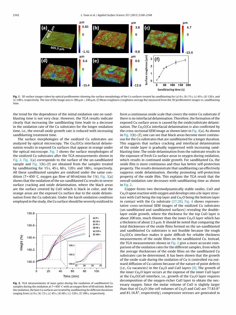
2162 L. Yuan et al. / Applied Surface Science 357 (2015) 2160–2168
Fig. 1. 3D surface images taken by optical profilometer showing the surface morphology of the Cu surfaces treated by sandblasting for (a) 0 s, (b) 15 s, (c) 45 s, (d) 120 s, and( ness
t
tbcits
anttFsbAdssaone
Fstr
e) 180 s, respectively. The size of the image area is 186 �m × 244 �m. (f) Mean roughime.
he trend for the dependence of the initial oxidation rate on sand-lasting time is not very clear. However, the TGA results indicatelearly that increasing the sandblasting time leads to a decreasen the oxidation rate of the Cu substrates for the longer oxidationime, i.e., the overall oxide growth rate is reduced with increasingandblasting treatment time.
The surface morphologies of the oxidized Cu substrates arenalyzed by optical microscopy. The Cu2O/Cu interfacial delami-ation results in exposed Cu surfaces that appear in orange underhe optical microscope. Fig. 3 shows the surface morphologies ofhe oxidized Cu substrates after the TGA measurements shown inig. 2. Fig. 3(a) corresponds to the surface of the un-sandblastedample and Fig. 3(b)–(f) are obtained from the samples treatedy sandblasting for 15 s, 45 s, 60 s, 120 s and 180 s, respectively.ll these sandblasted samples are oxidized under the same con-ition (T = 450 ◦C, oxygen gas flow of 60 ml/min for 1 h). Fig. 3(a)hows that the oxidation of the un-sandblasted Cu results in severeurface cracking and oxide delamination, where the black areasre the surface covered by CuO which is black in color, and the
range areas are the exposed Cu surface due to the oxide delami-ation from the Cu substrate. Under the harsh oxidation conditionmployed in the study, the Cu surface should be severely oxidized toig. 2. TGA measurements of mass gains during the oxidation of sandblasted Cuamples during the oxidation at T = 450 ◦C with an oxygen flow of 60 ml/min. Beforehe oxidation, the bare Cu surfaces are treated by sandblasting for different durationsanging from (a) 0 s, (b) 15 s, (c) 45 s, (d) 60 s, (c) 120 s, (f) 180 s, respectively.
(roughness average Ra) measured from the 3D profilometer images vs. sandblasting
form a continuous oxide scale that covers the entire Cu substrate ifthere is no interfacial delamination. Therefore, the formation of theexposed Cu surface areas is caused by the oxide/substrate delami-nation. The Cu2O/Cu interfacial delamination is also confirmed bythe cross-sectional SEM image as shown later in Fig. 4(a). As shownin Fig. 3(b)–(f), one can see that black areas become more continu-ous for the Cu substrates that are sandblasted for a longer duration.This suggests that surface cracking and interfacial delaminationof the oxide layer is gradually suppressed with increasing sand-blasting time. The oxide delamination from the substrate results inthe exposure of fresh Cu surface areas to oxygen during oxidation,which results in continued oxide growth. For sandblasted Cu, theoxide film is more continuous and thus has better self-protectionproperty. The results demonstrate that sandblasting can effectivelysuppress oxide delamination, thereby promoting self-protectionproperty of the oxide film. This explains the TGA result that theoverall oxidation rate decreases with sandblasting time as shownin Fig. 2.
Copper forms two thermodynamically stable oxides, CuO andCu2O upon reaction with oxygen and develops into a bi-layer struc-ture with CuO being the top layer and Cu2O being the bottom layerin contact with the Cu substrate [27,28]. Fig. 4 shows represen-tative cross-sectional SEM images of the oxidized Cu substrates(un-sandblasted and sandblasted surfaces) revealing the double-layer oxide growth, where the thickness for the top CuO layer isabout 200 nm, much thinner than the inner Cu2O layer which hasa thickness of about 2.5 �m. It should be noted that comparing thetotal thicknesses of the oxide films formed on the un-sandblastedand sandblasted Cu substrates is not feasible because the roughCu2O/Cu interface makes it quite difficult for reliable thicknessmeasurements of the oxide films on the sandblasted Cu. Instead,the TGA measurements shown in Fig. 2 give a more accurate com-parison of the oxidation rates for the different samples, from whichthe average thicknesses of the oxide films on the sandblasted Cusubstrates can be determined. It has been shown that the growthof the oxide scale during the oxidation of Cu is controlled via out-ward diffusion of Cu cations because of the nature of point defects(i.e., Cu vacancies) in the Cu2O and CuO layers [8]. The growth ofthe inner Cu2O layer occurs at the expense of the inner CuO layerat the Cu2O/CuO interface, i.e., growth of the Cu2O layer requires
decomposition of the oxygen-richer CuO layer to obtain the nec-essary oxygen. Since the molar volume of CuO is slightly largerthan that of Cu2O (the cell volumes of Cu2O and CuO are 77.83 A3and 81.16 A3, respectively), compressive stresses are generated in

L. Yuan et al. / Applied Surface Science 357 (2015) 2160–2168 2163
Fig. 3. Optical images of the Cu surfaces that are first treated by sandblasting for (a) 0 s, (b) 15 s, (c) 45 s, (d) 60 s, (c) 120 s, (f) 180 s, respectively, followed by oxidation atT s Cu. Pt
tifrmsfrfEslCTu
tcTtwsiwdfsFsiir
dpecTwr
= 450 ◦C for 1 h in an oxygen flow of 60 ml/min. Black area is CuO, and orange area ihe reader is referred to the web version of the article.)
he CuO layer by the volume change accompanying the CuO/Cu2Onterface reaction, which typically stimulates CuO NW (nanowire)ormation on the outer surface [28,29], as revealed in Fig. 4. As aesult, the CuO/Cu2O interface stress is released by CuO NW for-ation and the CuO/Cu2O interface remains intact and adherent as
hown by the SEM images in Fig. 4(c) and (d), which are obtainedrom the CuO/Cu2O interface regions marked by the dashed redectangles in Fig. 4(a) and (b), respectively. The lengths of the NWsormed on the oxidized Cu surfaces vary from 200 nm to several �m.DS spectra shown in Fig. 4(e) and (f) are collected from the top andecond oxide layers, confirming the existence of the CuO and Cu2Oayers. Fig. 4(g) shows an XRD pattern from the un-sandblastedu sample, showing the presence of both CuO and Cu2O peaks.he sandblasted Cu samples show the similar XRD patterns as then-sandblasted Cu sample.
The formation of Cu2O from the reaction (Cu + O2 → Cu2O) athe Cu2O/Cu interface results in large molar volume mismatch (theell volumes of Cu and Cu2O are 47.2 A3 and 77.83 A3, respectively).he ensuring difficulties in local volume accommodation give wayo the generation of large stresses in the Cu2O/Cu interface region,hich serve as the driving force for oxide delamination from the Cu
ubstrate. This can be evidenced from Fig. 4(a), which shows signif-cant delamination at the Cu2O/Cu interface. This is also consistent
ith the optical microscopy observations as shown in Fig. 3, whichemonstrate that the oxide delamination results in exposed Cu sur-ace. However compared to the un-sandblasted sample that showsignificant separation at the Cu2O/Cu interface, one can see fromig. 4(b) that the Cu2O layer adheres tightly to the roughened Cuubstrate. Pegging of the oxide film to the substrate by sandblast-ng provides the interlocking mechanical mechanism that resultsn improvement in oxide adherence and thereby better oxidationesistance as revealed in the TGA measurements shown in Fig. 2.
To confirm that the improved Cu2O/Cu interfacial adhesionescribed above is related to sandblasting, the oxidation mor-hologies around individual craters generated by sandblasting arexamined. Fig. 5(a) shows a 3D profile surface image of a single
rater formed on a sandblasted Cu substrate before oxidation.he diameter of the crater is about 150 �m with a ramp area,hich corresponds well with the round shape and the diameterange of the spherical glass beads used for sandblasting. The crater
rior to oxidation. (For interpretation of the references to color in this figure legend,
experiences different levels of deformation from the ramp tothe bottom area, as expected from the different stresses exertedduring sandblasting. The stress induced-deformation increasesfrom rim area to ramp area, and reaches maximum at the craterbottom. Fig. 5(b) shows an SEM image of an oxidized Cu substratewhich is treated by sandblasting for 15 s before the oxidation at450 ◦C. Several craters are still visible even after the oxidation,as marked by red circles. Stress-induced cracks in the oxide filmare also found on the surface. However, one can see that thesesurface cracks are terminated at the rim area of the craters, i.e., thepropagation of cracks in the oxide film is stopped by the presenceof craters. This suggests that the oxide film formed in the craterarea has better oxide/substrate mechanical adhesion.
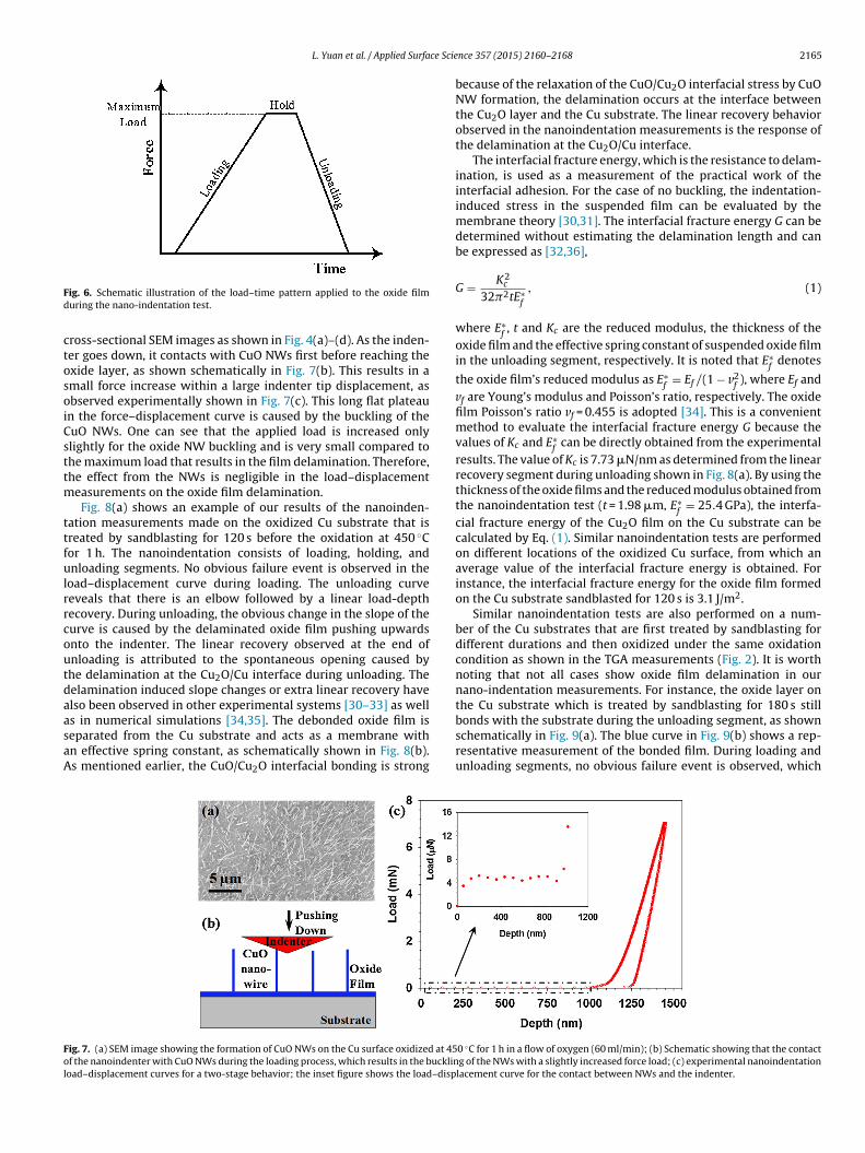
It can now be inferred from the observation shown in Fig. 5 thatthe sandblasting induced craters can inhibit cracking propagationin the oxide layer during oxidation. This corroborates well with theTGA observation shown in Fig. 2, i.e., the oxidation rate decreaseswith sandblasting time. Their correlation indicates that the sand-blasting treatment of the Cu surfaces can effectively promote theoxide adhesion with the Cu substrate as seen in Fig. 4, therebyresulting in the improved self protection of the oxide film. To bet-ter elucidate the mechanical adhesion of the oxide film with theCu substrate, we employ the nanoindentation technique to mea-sure and evaluate the bonding energy between the oxide film andthe Cu substrate. Fig. 6 schematically shows the load–time pat-tern applied to the oxide film during the nanoindentation test,which includes a constant-rate-loading segment, a hold segment,and a constant-rate-unloading segment, as described in materialand methods section.
The nanoindentation induces a complex stress field in theoxide/metal interface region, which can lead to delaminationof the oxide layer at the Cu2O/Cu interface. After delamination,the debonded oxide film may be suspended over the substrateunder small load and can be considered as a membrane, and thusthe interfacial delamination fracture energy can be analyzed bythe load-depth data using the membrane theory [30–32]. The
oxidation of Cu typically results in the growth of CuO NWs, asshown in the SEM image in Fig. 7(a), taken from an un-delaminatedoxide film. No cracks are formed in these un-delaminated surfaceareas. The growth of CuO NWs can be also confirmed from the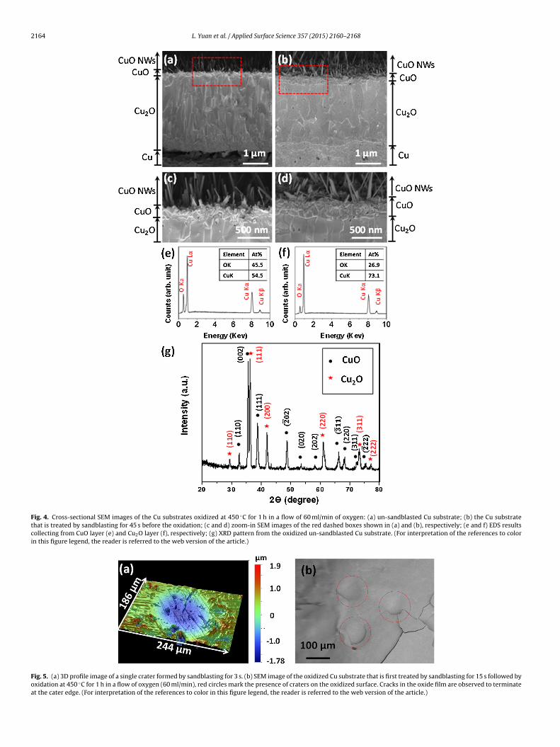
2164 L. Yuan et al. / Applied Surface Science 357 (2015) 2160–2168
Fig. 4. Cross-sectional SEM images of the Cu substrates oxidized at 450 ◦C for 1 h in a flow of 60 ml/min of oxygen: (a) un-sandblasted Cu substrate; (b) the Cu substratethat is treated by sandblasting for 45 s before the oxidation; (c and d) zoom-in SEM images of the red dashed boxes shown in (a) and (b), respectively; (e and f) EDS resultscollecting from CuO layer (e) and Cu2O layer (f), respectively; (g) XRD pattern from the oxidized un-sandblasted Cu substrate. (For interpretation of the references to colorin this figure legend, the reader is referred to the web version of the article.)
Fig. 5. (a) 3D profile image of a single crater formed by sandblasting for 3 s. (b) SEM image of the oxidized Cu substrate that is first treated by sandblasting for 15 s followed byoxidation at 450 ◦C for 1 h in a flow of oxygen (60 ml/min), red circles mark the presence of craters on the oxidized surface. Cracks in the oxide film are observed to terminateat the cater edge. (For interpretation of the references to color in this figure legend, the reader is referred to the web version of the article.)
L. Yuan et al. / Applied Surface Scie
Fd
ctosoiCsttm
ttfulrrcoutdaasaA
Fol
ig. 6. Schematic illustration of the load–time pattern applied to the oxide filmuring the nano-indentation test.
ross-sectional SEM images as shown in Fig. 4(a)–(d). As the inden-er goes down, it contacts with CuO NWs first before reaching thexide layer, as shown schematically in Fig. 7(b). This results in amall force increase within a large indenter tip displacement, asbserved experimentally shown in Fig. 7(c). This long flat plateaun the force–displacement curve is caused by the buckling of theuO NWs. One can see that the applied load is increased onlylightly for the oxide NW buckling and is very small compared tohe maximum load that results in the film delamination. Therefore,he effect from the NWs is negligible in the load–displacement
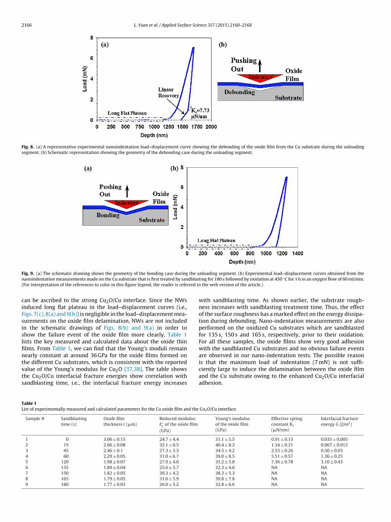
easurements on the oxide film delamination.Fig. 8(a) shows an example of our results of the nanoinden-
ation measurements made on the oxidized Cu substrate that isreated by sandblasting for 120 s before the oxidation at 450 ◦Cor 1 h. The nanoindentation consists of loading, holding, andnloading segments. No obvious failure event is observed in the
oad–displacement curve during loading. The unloading curveeveals that there is an elbow followed by a linear load-depthecovery. During unloading, the obvious change in the slope of theurve is caused by the delaminated oxide film pushing upwardsnto the indenter. The linear recovery observed at the end ofnloading is attributed to the spontaneous opening caused byhe delamination at the Cu2O/Cu interface during unloading. Theelamination induced slope changes or extra linear recovery havelso been observed in other experimental systems [30–33] as well
s in numerical simulations [34,35]. The debonded oxide film iseparated from the Cu substrate and acts as a membrane withn effective spring constant, as schematically shown in Fig. 8(b).s mentioned earlier, the CuO/Cu2O interfacial bonding is strongig. 7. (a) SEM image showing the formation of CuO NWs on the Cu surface oxidized at 45f the nanoindenter with CuO NWs during the loading process, which results in the bucklinoad–displacement curves for a two-stage behavior; the inset figure shows the load–disp
nce 357 (2015) 2160–2168 2165
because of the relaxation of the CuO/Cu2O interfacial stress by CuONW formation, the delamination occurs at the interface betweenthe Cu2O layer and the Cu substrate. The linear recovery behaviorobserved in the nanoindentation measurements is the response ofthe delamination at the Cu2O/Cu interface.
The interfacial fracture energy, which is the resistance to delam-ination, is used as a measurement of the practical work of theinterfacial adhesion. For the case of no buckling, the indentation-induced stress in the suspended film can be evaluated by themembrane theory [30,31]. The interfacial fracture energy G can bedetermined without estimating the delamination length and canbe expressed as [32,36],
G = K2c
32�2tE∗f
, (1)
where E∗f, t and Kc are the reduced modulus, the thickness of the
oxide film and the effective spring constant of suspended oxide filmin the unloading segment, respectively. It is noted that E∗
fdenotes
the oxide film’s reduced modulus as E∗f
= Ef /(1 − v2f), where Ef and
vf are Young’s modulus and Poisson’s ratio, respectively. The oxidefilm Poisson’s ratio vf = 0.455 is adopted [34]. This is a convenientmethod to evaluate the interfacial fracture energy G because thevalues of Kc and E∗
fcan be directly obtained from the experimental
results. The value of Kc is 7.73 �N/nm as determined from the linearrecovery segment during unloading shown in Fig. 8(a). By using thethickness of the oxide films and the reduced modulus obtained fromthe nanoindentation test (t = 1.98 �m, E∗
f= 25.4 GPa), the interfa-
cial fracture energy of the Cu2O film on the Cu substrate can becalculated by Eq. (1). Similar nanoindentation tests are performedon different locations of the oxidized Cu surface, from which anaverage value of the interfacial fracture energy is obtained. Forinstance, the interfacial fracture energy for the oxide film formedon the Cu substrate sandblasted for 120 s is 3.1 J/m2.
Similar nanoindentation tests are also performed on a num-ber of the Cu substrates that are first treated by sandblasting fordifferent durations and then oxidized under the same oxidationcondition as shown in the TGA measurements (Fig. 2). It is worthnoting that not all cases show oxide film delamination in ournano-indentation measurements. For instance, the oxide layer onthe Cu substrate which is treated by sandblasting for 180 s still
bonds with the substrate during the unloading segment, as shownschematically in Fig. 9(a). The blue curve in Fig. 9(b) shows a rep-resentative measurement of the bonded film. During loading andunloading segments, no obvious failure event is observed, which0 ◦C for 1 h in a flow of oxygen (60 ml/min); (b) Schematic showing that the contactg of the NWs with a slightly increased force load; (c) experimental nanoindentationlacement curve for the contact between NWs and the indenter.
2166 L. Yuan et al. / Applied Surface Science 357 (2015) 2160–2168
Fig. 8. (a) A representative experimental nanoindentation load–displacement curve showing the debonding of the oxide film from the Cu substrate during the unloadingsegment. (b) Schematic representation showing the geometry of the debonding case during the unloading segment.
F the un dblas( rred to
ciFsislfintvts
TL
ig. 9. (a) The schematic drawing shows the geometry of the bonding case duringanoindentation measurements made on the Cu substrate that is first treated by sanFor interpretation of the references to color in this figure legend, the reader is refe
an be ascribed to the strong Cu2O/Cu interface. Since the NWsnduced long flat plateau in the load–displacement curves (i.e.,igs. 7(c), 8(a) and 9(b)) is negligible in the load–displacement mea-urements on the oxide film delamination, NWs are not includedn the schematic drawings of Figs. 8(b) and 9(a) in order tohow the failure event of the oxide film more clearly. Table 1ists the key measured and calculated data about the oxide thinlms. From Table 1, we can find that the Young’s moduli remainearly constant at around 36 GPa for the oxide films formed onhe different Cu substrates, which is consistent with the reported
alue of the Young’s modulus for Cu2O [37,38]. The table showshe Cu2O/Cu interfacial fracture energies show correlation withandblasting time, i.e., the interfacial fracture energy increasesable 1ist of experimentally measured and calculated parameters for the Cu oxide film and the
Sample # Sandblastingtime (s)
Oxide filmthickness t (�m)
Reduced modulusE∗
fof the oxide film
(GPa)
1 0 3.06 ± 0.15 24.7 ± 4.4
2 15 2.66 ± 0.08 32.1 ± 6.5
3 45 2.46 ± 0.1 27.3 ± 3.3
4 60 2.29 ± 0.05 31.0 ± 6.7
5 120 1.98 ± 0.07 27.9 ± 4.6
6 135 1.89 ± 0.04 25.6 ± 3.7
7 150 1.82 ± 0.05 30.3 ± 4.2
8 165 1.79 ± 0.05 31.6 ± 5.9
9 180 1.77 ± 0.03 26.0 ± 5.2
nloading segment. (b) Experimental load–displacement curves obtained from theting for 180 s followed by oxidation at 450 ◦C for 1 h in an oxygen flow of 60 ml/min.
the web version of the article.)
with sandblasting time. As shown earlier, the substrate rough-ness increases with sandblasting treatment time. Thus, the effectof the surface roughness has a marked effect on the energy dissipa-tion during debonding. Nano-indentation measurements are alsoperformed on the oxidized Cu substrates which are sandblastedfor 135 s, 150 s and 165 s, respectively, prior to their oxidation.For all these samples, the oxide films show very good adhesionwith the sandblasted Cu substrates and no obvious failure eventsare observed in our nano-indentation tests. The possible reasonis that the maximum load of indentation (7 mN) is not suffi-
ciently large to induce the delamination between the oxide filmand the Cu substrate owing to the enhanced Cu2O/Cu interfacialadhesion.Cu2O/Cu interface.
Young’s modulusof the oxide film(GPa)
Effective springconstant Kc
(�N/nm)
Interfacial fractureenergy G (J/m2)
31.1 ± 5.5 0.91 ± 0.13 0.035 ± 0.00540.4 ± 8.2 1.34 ± 0.21 0.067 ± 0.01234.5 ± 4.2 2.53 ± 0.26 0.30 ± 0.0339.0 ± 8.5 5.51 ± 0.57 1.36 ± 0.2535.2 ± 5.8 7.36 ± 0.78 3.10 ± 0.4332.3 ± 4.6 NA NA38.3 ± 5.3 NA NA39.8 ± 7.8 NA NA32.8 ± 6.6 NA NA
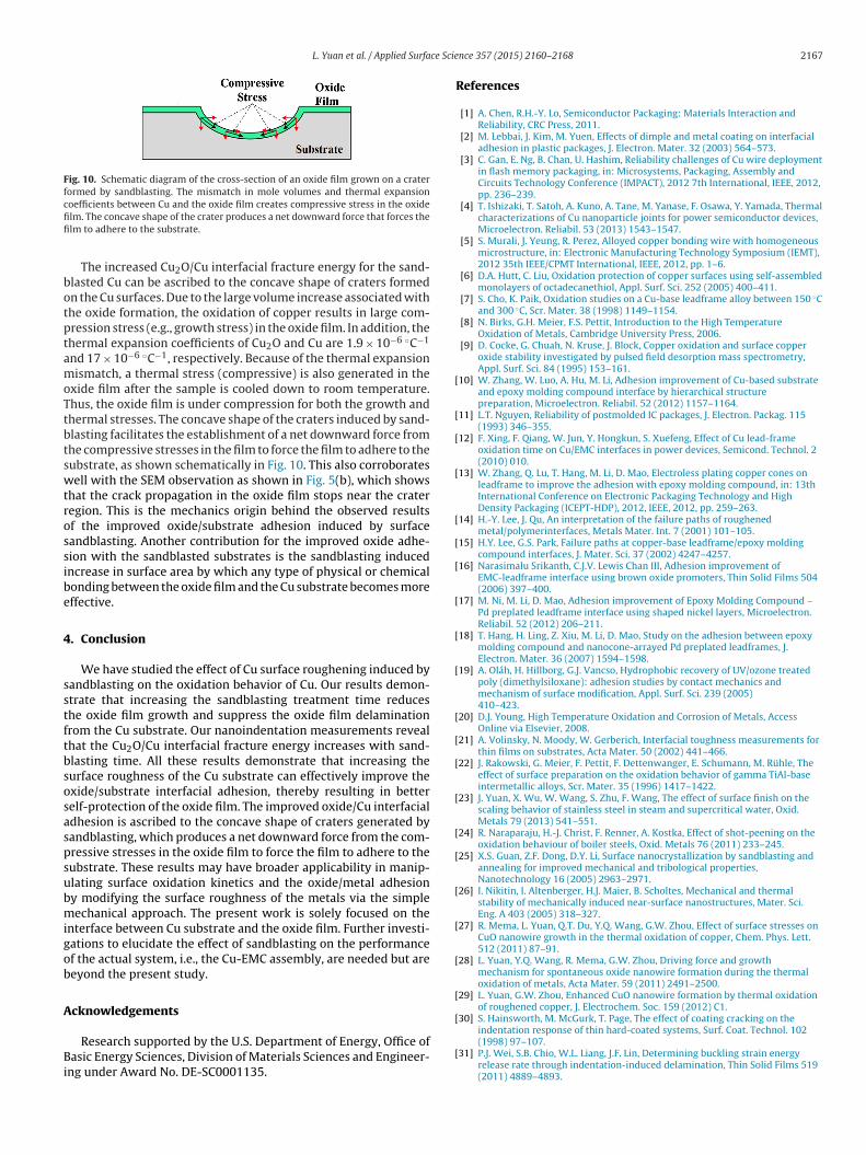
L. Yuan et al. / Applied Surface Scie
Fig. 10. Schematic diagram of the cross-section of an oxide film grown on a craterformed by sandblasting. The mismatch in mole volumes and thermal expansioncfifi
botptamoTtbtswtrossibe
4
sstftbsosaspsubmigob
A
Bi
[
[
[
[
[
[
[
[
[
[
[
[
[
[
[
[
[
[
[
[
[
oefficients between Cu and the oxide film creates compressive stress in the oxidelm. The concave shape of the crater produces a net downward force that forces thelm to adhere to the substrate.
The increased Cu2O/Cu interfacial fracture energy for the sand-lasted Cu can be ascribed to the concave shape of craters formedn the Cu surfaces. Due to the large volume increase associated withhe oxide formation, the oxidation of copper results in large com-ression stress (e.g., growth stress) in the oxide film. In addition, thehermal expansion coefficients of Cu2O and Cu are 1.9 × 10⁻⁶ ◦C−1
nd 17 × 10−6 ◦C−1, respectively. Because of the thermal expansionismatch, a thermal stress (compressive) is also generated in the
xide film after the sample is cooled down to room temperature.hus, the oxide film is under compression for both the growth andhermal stresses. The concave shape of the craters induced by sand-lasting facilitates the establishment of a net downward force fromhe compressive stresses in the film to force the film to adhere to theubstrate, as shown schematically in Fig. 10. This also corroboratesell with the SEM observation as shown in Fig. 5(b), which shows
hat the crack propagation in the oxide film stops near the crateregion. This is the mechanics origin behind the observed resultsf the improved oxide/substrate adhesion induced by surfaceandblasting. Another contribution for the improved oxide adhe-ion with the sandblasted substrates is the sandblasting inducedncrease in surface area by which any type of physical or chemicalonding between the oxide film and the Cu substrate becomes moreffective.
. Conclusion
We have studied the effect of Cu surface roughening induced byandblasting on the oxidation behavior of Cu. Our results demon-trate that increasing the sandblasting treatment time reduceshe oxide film growth and suppress the oxide film delaminationrom the Cu substrate. Our nanoindentation measurements revealhat the Cu2O/Cu interfacial fracture energy increases with sand-lasting time. All these results demonstrate that increasing theurface roughness of the Cu substrate can effectively improve thexide/substrate interfacial adhesion, thereby resulting in betterelf-protection of the oxide film. The improved oxide/Cu interfacialdhesion is ascribed to the concave shape of craters generated byandblasting, which produces a net downward force from the com-ressive stresses in the oxide film to force the film to adhere to theubstrate. These results may have broader applicability in manip-lating surface oxidation kinetics and the oxide/metal adhesiony modifying the surface roughness of the metals via the simpleechanical approach. The present work is solely focused on the
nterface between Cu substrate and the oxide film. Further investi-ations to elucidate the effect of sandblasting on the performancef the actual system, i.e., the Cu-EMC assembly, are needed but areeyond the present study.
cknowledgements
Research supported by the U.S. Department of Energy, Office ofasic Energy Sciences, Division of Materials Sciences and Engineer-
ng under Award No. DE-SC0001135.
[
nce 357 (2015) 2160–2168 2167
References
[1] A. Chen, R.H.-Y. Lo, Semiconductor Packaging: Materials Interaction andReliability, CRC Press, 2011.
[2] M. Lebbai, J. Kim, M. Yuen, Effects of dimple and metal coating on interfacialadhesion in plastic packages, J. Electron. Mater. 32 (2003) 564–573.
[3] C. Gan, E. Ng, B. Chan, U. Hashim, Reliability challenges of Cu wire deploymentin flash memory packaging, in: Microsystems, Packaging, Assembly andCircuits Technology Conference (IMPACT), 2012 7th International, IEEE, 2012,pp. 236–239.
[4] T. Ishizaki, T. Satoh, A. Kuno, A. Tane, M. Yanase, F. Osawa, Y. Yamada, Thermalcharacterizations of Cu nanoparticle joints for power semiconductor devices,Microelectron. Reliabil. 53 (2013) 1543–1547.
[5] S. Murali, J. Yeung, R. Perez, Alloyed copper bonding wire with homogeneousmicrostructure, in: Electronic Manufacturing Technology Symposium (IEMT),2012 35th IEEE/CPMT International, IEEE, 2012, pp. 1–6.
[6] D.A. Hutt, C. Liu, Oxidation protection of copper surfaces using self-assembledmonolayers of octadecanethiol, Appl. Surf. Sci. 252 (2005) 400–411.
[7] S. Cho, K. Paik, Oxidation studies on a Cu-base leadframe alloy between 150 ◦Cand 300 ◦C, Scr. Mater. 38 (1998) 1149–1154.
[8] N. Birks, G.H. Meier, F.S. Pettit, Introduction to the High TemperatureOxidation of Metals, Cambridge University Press, 2006.
[9] D. Cocke, G. Chuah, N. Kruse, J. Block, Copper oxidation and surface copperoxide stability investigated by pulsed field desorption mass spectrometry,Appl. Surf. Sci. 84 (1995) 153–161.
10] W. Zhang, W. Luo, A. Hu, M. Li, Adhesion improvement of Cu-based substrateand epoxy molding compound interface by hierarchical structurepreparation, Microelectron. Reliabil. 52 (2012) 1157–1164.
11] L.T. Nguyen, Reliability of postmolded IC packages, J. Electron. Packag. 115(1993) 346–355.
12] F. Xing, F. Qiang, W. Jun, Y. Hongkun, S. Xuefeng, Effect of Cu lead-frameoxidation time on Cu/EMC interfaces in power devices, Semicond. Technol. 2(2010) 010.
13] W. Zhang, Q. Lu, T. Hang, M. Li, D. Mao, Electroless plating copper cones onleadframe to improve the adhesion with epoxy molding compound, in: 13thInternational Conference on Electronic Packaging Technology and HighDensity Packaging (ICEPT-HDP), 2012, IEEE, 2012, pp. 259–263.
14] H.-Y. Lee, J. Qu, An interpretation of the failure paths of roughenedmetal/polymerinterfaces, Metals Mater. Int. 7 (2001) 101–105.
15] H.Y. Lee, G.S. Park, Failure paths at copper-base leadframe/epoxy moldingcompound interfaces, J. Mater. Sci. 37 (2002) 4247–4257.
16] Narasimalu Srikanth, C.J.V. Lewis Chan III, Adhesion improvement ofEMC-leadframe interface using brown oxide promoters, Thin Solid Films 504(2006) 397–400.
17] M. Ni, M. Li, D. Mao, Adhesion improvement of Epoxy Molding Compound –Pd preplated leadframe interface using shaped nickel layers, Microelectron.Reliabil. 52 (2012) 206–211.
18] T. Hang, H. Ling, Z. Xiu, M. Li, D. Mao, Study on the adhesion between epoxymolding compound and nanocone-arrayed Pd preplated leadframes, J.Electron. Mater. 36 (2007) 1594–1598.
19] A. Oláh, H. Hillborg, G.J. Vancso, Hydrophobic recovery of UV/ozone treatedpoly (dimethylsiloxane): adhesion studies by contact mechanics andmechanism of surface modification, Appl. Surf. Sci. 239 (2005)410–423.
20] D.J. Young, High Temperature Oxidation and Corrosion of Metals, AccessOnline via Elsevier, 2008.
21] A. Volinsky, N. Moody, W. Gerberich, Interfacial toughness measurements forthin films on substrates, Acta Mater. 50 (2002) 441–466.
22] J. Rakowski, G. Meier, F. Pettit, F. Dettenwanger, E. Schumann, M. Rühle, Theeffect of surface preparation on the oxidation behavior of gamma TiAl-baseintermetallic alloys, Scr. Mater. 35 (1996) 1417–1422.
23] J. Yuan, X. Wu, W. Wang, S. Zhu, F. Wang, The effect of surface finish on thescaling behavior of stainless steel in steam and supercritical water, Oxid.Metals 79 (2013) 541–551.
24] R. Naraparaju, H.-J. Christ, F. Renner, A. Kostka, Effect of shot-peening on theoxidation behaviour of boiler steels, Oxid. Metals 76 (2011) 233–245.
25] X.S. Guan, Z.F. Dong, D.Y. Li, Surface nanocrystallization by sandblasting andannealing for improved mechanical and tribological properties,Nanotechnology 16 (2005) 2963–2971.
26] I. Nikitin, I. Altenberger, H.J. Maier, B. Scholtes, Mechanical and thermalstability of mechanically induced near-surface nanostructures, Mater. Sci.Eng. A 403 (2005) 318–327.
27] R. Mema, L. Yuan, Q.T. Du, Y.Q. Wang, G.W. Zhou, Effect of surface stresses onCuO nanowire growth in the thermal oxidation of copper, Chem. Phys. Lett.512 (2011) 87–91.
28] L. Yuan, Y.Q. Wang, R. Mema, G.W. Zhou, Driving force and growthmechanism for spontaneous oxide nanowire formation during the thermaloxidation of metals, Acta Mater. 59 (2011) 2491–2500.
29] L. Yuan, G.W. Zhou, Enhanced CuO nanowire formation by thermal oxidationof roughened copper, J. Electrochem. Soc. 159 (2012) C1.
30] S. Hainsworth, M. McGurk, T. Page, The effect of coating cracking on theindentation response of thin hard-coated systems, Surf. Coat. Technol. 102
(1998) 97–107.31] P.J. Wei, S.B. Chio, W.L. Liang, J.F. Lin, Determining buckling strain energyrelease rate through indentation-induced delamination, Thin Solid Films 519(2011) 4889–4893.

2 ce Scie
[
[
[
[
[
[37] G.W. Zhou, J.C. Yang, Formation of quasi-one-dimensional Cu2O structuresby in situ oxidation of Cu (100), Phys. Rev. Lett. 89 (2002)
168 L. Yuan et al. / Applied Surfa
32] P.J. Wei, W.L. Liang, C.F. Ai, J.F. Lin, A new method for determining the strainenergy release rate of an interface via force-depth data of nanoindentationtests, Nanotechnology 20 (2009) 025701.
33] J. Chen, S. Bull, Indentation fracture and toughness assessment for thin opticalcoatings on glass, J. Phys. D: Appl. Phys. 40 (2007) 5401.
34] A. Abdul-Baqi, E. Van der Giessen, Delamination of a strong film from a ductilesubstrate during indentation unloading, J. Mater. Res. 16 (2001) 1396–1407.
35] J. Chen, S. Bull, Finite element analysis of contact induced adhesion failure inmultilayer coatings with weak interfaces, Thin Solid Films 517 (2009)3704–3711.
[
nce 357 (2015) 2160–2168
36] D. Marshall, A. Evans, Measurement of adherence of residually stressed thinfilms by indentation. I. Mechanics of interface delamination, J. Appl. Phys. 56(1984) 2632–2638.
106101.38] H.J. Frost, M.F. Ashby, Deformation Mechanism Maps: The Plasticity and
Creep of Metals and Ceramics, Pergamon Press, 1982.


![Random Process Examples - Binghamton Universityws2.binghamton.edu/fowler/fowler personal page/EE521_files/V-3 RP Examples_2007.pdf3/23 Ex. #1: D-T White Noise Also, let x[k] be Gaussian](https://img.pdfslide.us/doc/110x75/5e8c0b695e76293fb049ee9a/random-process-examples-binghamton-personal-pageee521filesv-3-rp-examples2007pdf.jpg)

![The crystal structural evolution of nano-Si anode …ws2.binghamton.edu/me/Zhou/Zhou-publications/Solid-state...H.Li et al. / Solid State Ionics 135 (2000) 181–191 183 observed [15–17]](https://img.pdfslide.us/doc/110x75/5f53b288ac045a3b1749eaed/the-crystal-structural-evolution-of-nano-si-anode-ws2-hli-et-al-solid-state.jpg)