Embed Size (px)
Citation preview
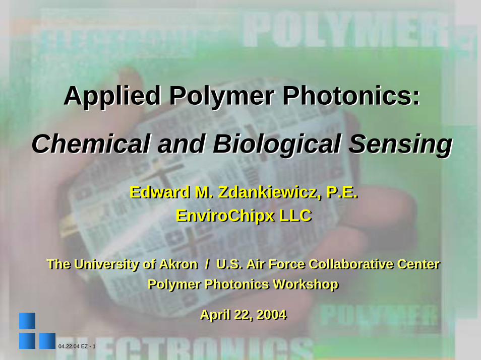
Applied Polymer Photonics:
Chemical and Biological Sensing
Applied Polymer Photonics:
Chemical and Biological Sensing
The University of Akron / U.S. Air Force Collaborative CenterPolymer Photonics Workshop
April 22, 2004
The University of Akron / U.S. Air Force Collaborative CenterPolymer Photonics Workshop
April 22, 2004
04.22.04 EZ - 1
Edward M. Zdankiewicz, P.E.EnviroChipx LLC
Edward M. Zdankiewicz, P.E.EnviroChipx LLC
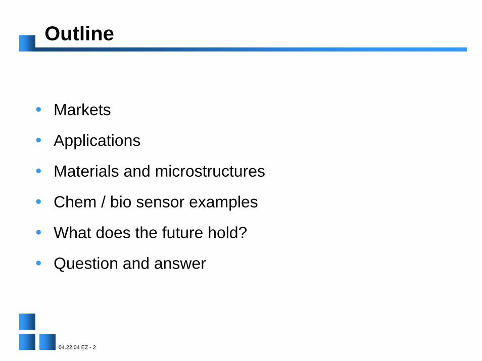
Outline
• Markets
• Applications
• Materials and microstructures
• Chem / bio sensor examples
• What does the future hold?
• Question and answer
04.22.04 EZ - 2
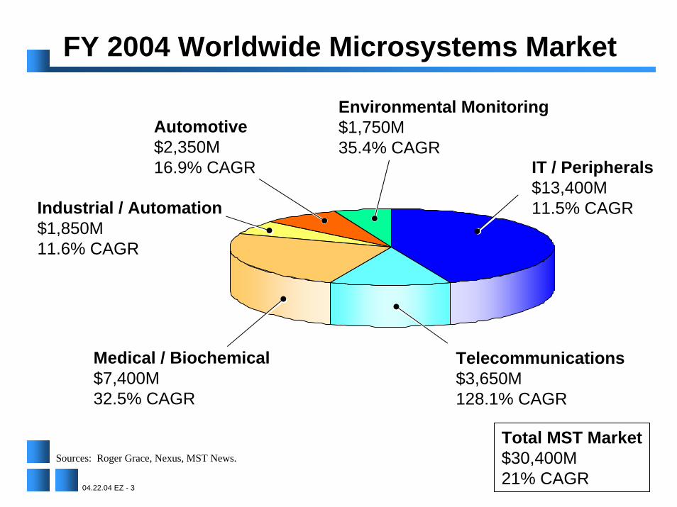
FY 2004 Worldwide Microsystems Market
IT / Peripherals$13,400M11.5% CAGR
Environmental Monitoring$1,750M35.4% CAGR
Automotive$2,350M16.9% CAGR
Industrial / Automation$1,850M11.6% CAGR
Medical / Biochemical$7,400M32.5% CAGR
Telecommunications$3,650M128.1% CAGR
Total MST Market$30,400M21% CAGR
Sources: Roger Grace, Nexus, MST News.
04.22.04 EZ - 3
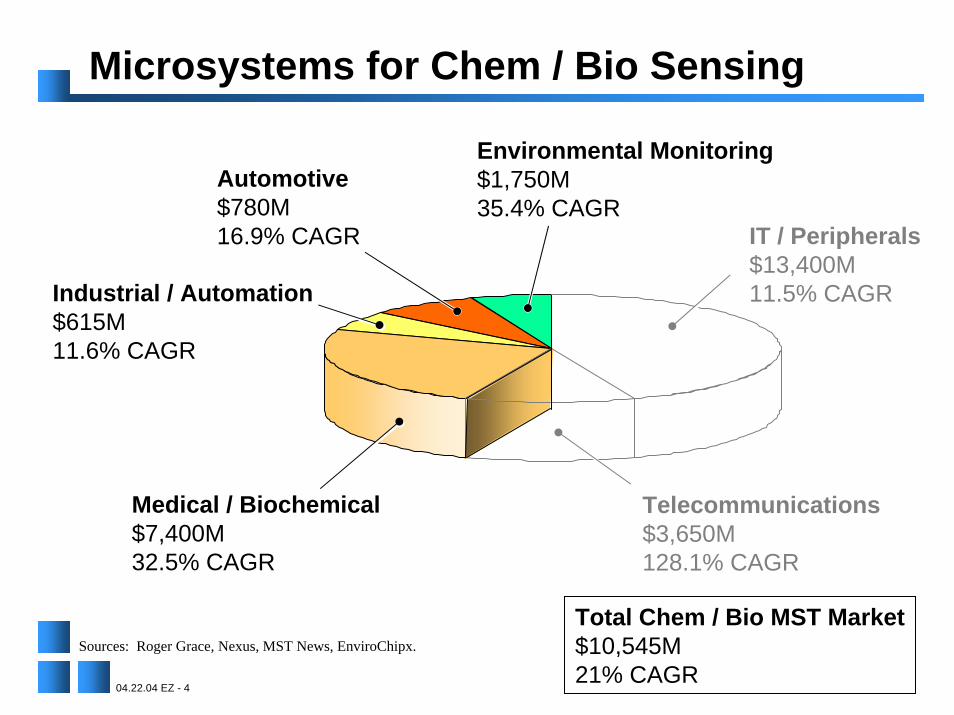
Microsystems for Chem / Bio Sensing
IT / Peripherals$13,400M11.5% CAGR
Environmental Monitoring$1,750M35.4% CAGR
Automotive$780M16.9% CAGR
Industrial / Automation$615M11.6% CAGR
Medical / Biochemical$7,400M32.5% CAGR
Telecommunications$3,650M128.1% CAGR
Total Chem / Bio MST Market$10,545M21% CAGR
Sources: Roger Grace, Nexus, MST News, EnviroChipx.
04.22.04 EZ - 4
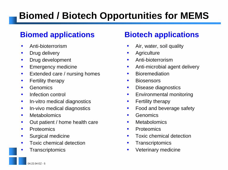
Biomed / Biotech Opportunities for MEMS
Biotech applicationsBiomed applications• Air, water, soil quality• Agriculture • Anti-bioterrorism• Anti-microbial agent delivery• Bioremediation• Biosensors• Disease diagnostics• Environmental monitoring• Fertility therapy• Food and beverage safety• Genomics• Metabolomics• Proteomics• Toxic chemical detection• Transcriptomics• Veterinary medicine
• Anti-bioterrorism• Drug delivery• Drug development• Emergency medicine• Extended care / nursing homes• Fertility therapy• Genomics• Infection control• In-vitro medical diagnostics• In-vivo medical diagnostics• Metabolomics• Out patient / home health care• Proteomics• Surgical medicine• Toxic chemical detection• Transcriptomics
04.22.04 EZ - 5
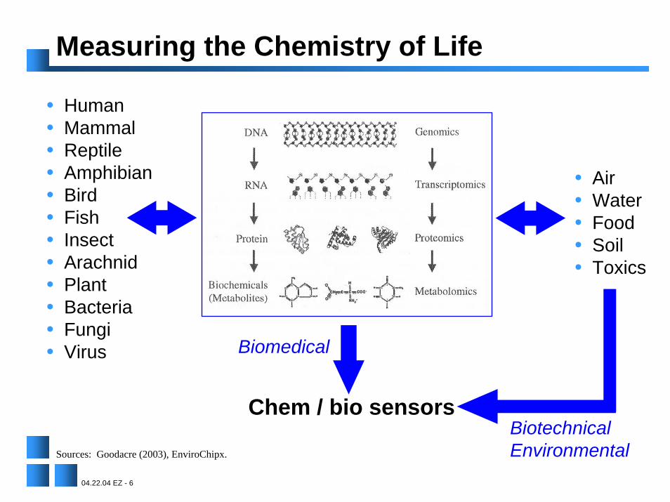
Measuring the Chemistry of Life
• Human• Mammal• Reptile• Amphibian• Bird• Fish • Insect• Arachnid• Plant• Bacteria• Fungi• Virus
04.22.04 EZ - 6
Sources: Goodacre (2003), EnviroChipx.
Chem / bio sensors
• Air• Water• Food• Soil• Toxics
Biomedical
BiotechnicalEnvironmental
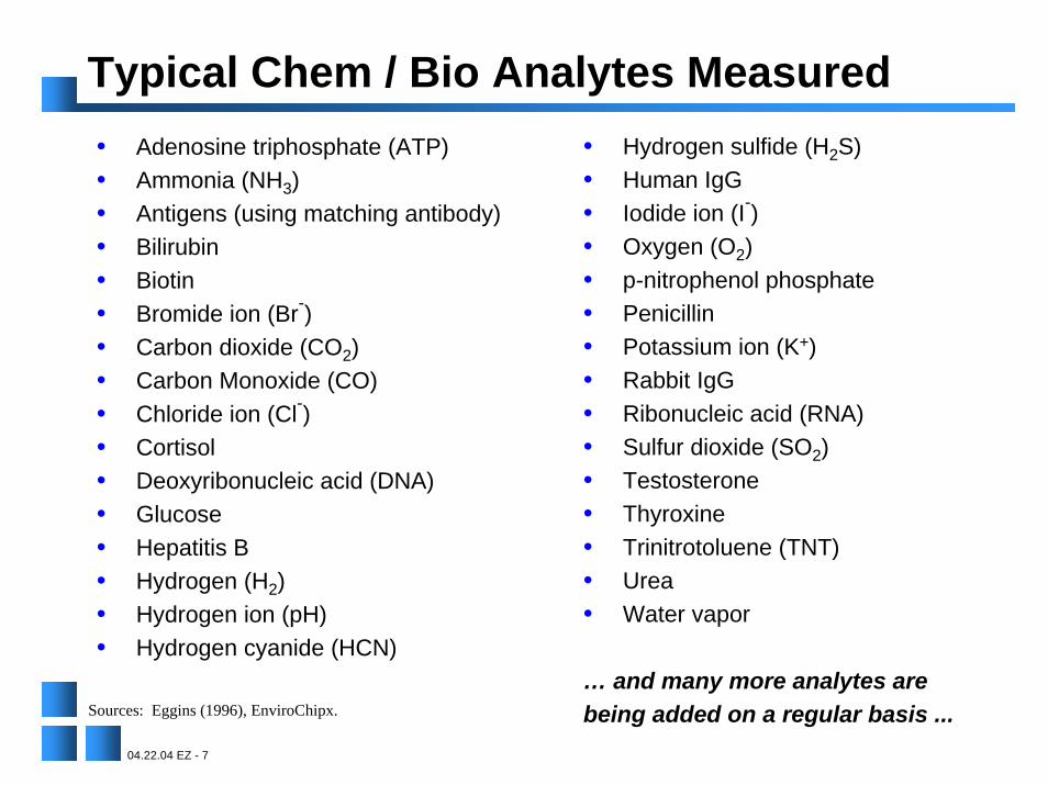
Typical Chem / Bio Analytes Measured• Hydrogen sulfide (H2S)• Human IgG• Iodide ion (I-)• Oxygen (O2)• p-nitrophenol phosphate• Penicillin• Potassium ion (K+)• Rabbit IgG• Ribonucleic acid (RNA)• Sulfur dioxide (SO2)• Testosterone• Thyroxine• Trinitrotoluene (TNT)• Urea• Water vapor
… and many more analytes arebeing added on a regular basis ...
• Adenosine triphosphate (ATP)• Ammonia (NH3)• Antigens (using matching antibody)• Bilirubin• Biotin• Bromide ion (Br-)• Carbon dioxide (CO2)• Carbon Monoxide (CO)• Chloride ion (Cl-)• Cortisol• Deoxyribonucleic acid (DNA)• Glucose• Hepatitis B• Hydrogen (H2)• Hydrogen ion (pH)• Hydrogen cyanide (HCN)
Sources: Eggins (1996), EnviroChipx.
04.22.04 EZ - 7
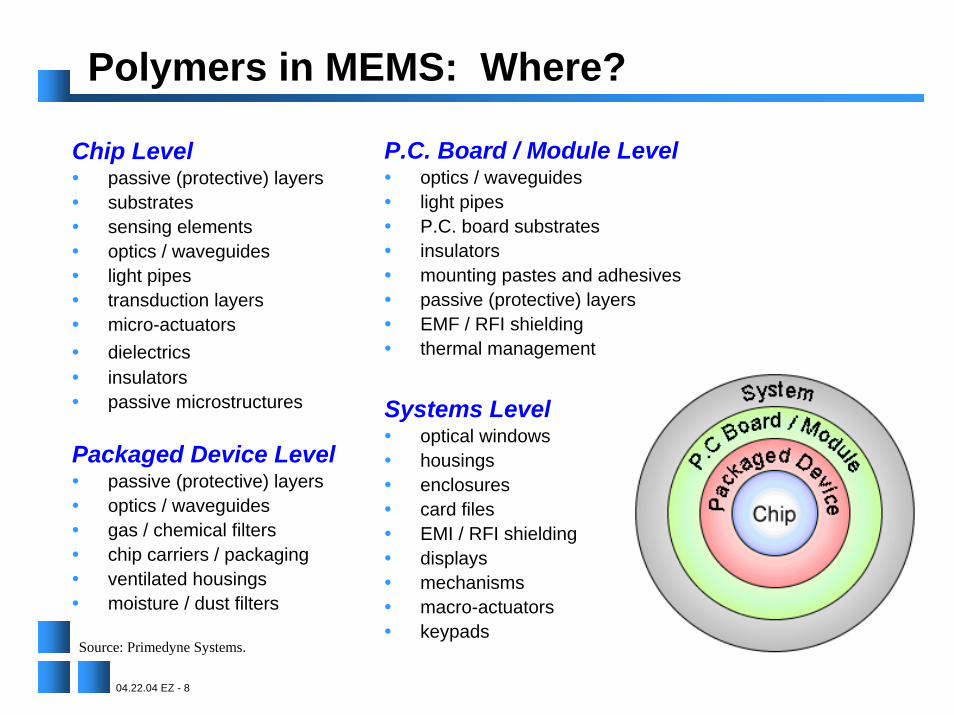
Polymers in MEMS: Where?
Source: Primedyne Systems.
Chip Level• passive (protective) layers• substrates• sensing elements• optics / waveguides• light pipes• transduction layers• micro-actuators• dielectrics• insulators• passive microstructures
Packaged Device Level• passive (protective) layers• optics / waveguides• gas / chemical filters• chip carriers / packaging• ventilated housings• moisture / dust filters
P.C. Board / Module Level• optics / waveguides• light pipes • P.C. board substrates• insulators• mounting pastes and adhesives• passive (protective) layers• EMF / RFI shielding• thermal management
Systems Level• optical windows• housings• enclosures• card files• EMI / RFI shielding• displays• mechanisms• macro-actuators• keypads
04.22.04 EZ - 8
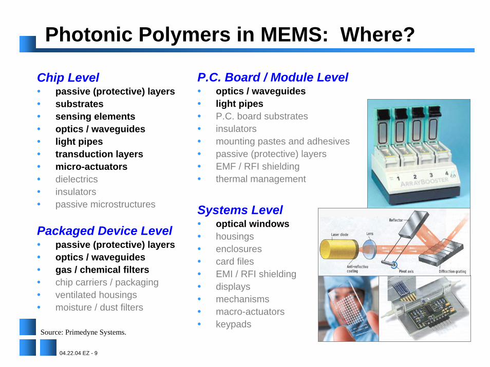
Photonic Polymers in MEMS: Where?
Chip Level• passive (protective) layers• substrates• sensing elements• optics / waveguides• light pipes• transduction layers• micro-actuators• dielectrics• insulators• passive microstructures
Packaged Device Level• passive (protective) layers• optics / waveguides• gas / chemical filters• chip carriers / packaging• ventilated housings• moisture / dust filters
P.C. Board / Module Level• optics / waveguides• light pipes• P.C. board substrates• insulators• mounting pastes and adhesives• passive (protective) layers• EMF / RFI shielding• thermal management
Systems Level• optical windows• housings• enclosures• card files• EMI / RFI shielding• displays• mechanisms• macro-actuators• keypads
Source: Primedyne Systems.
04.22.04 EZ - 9
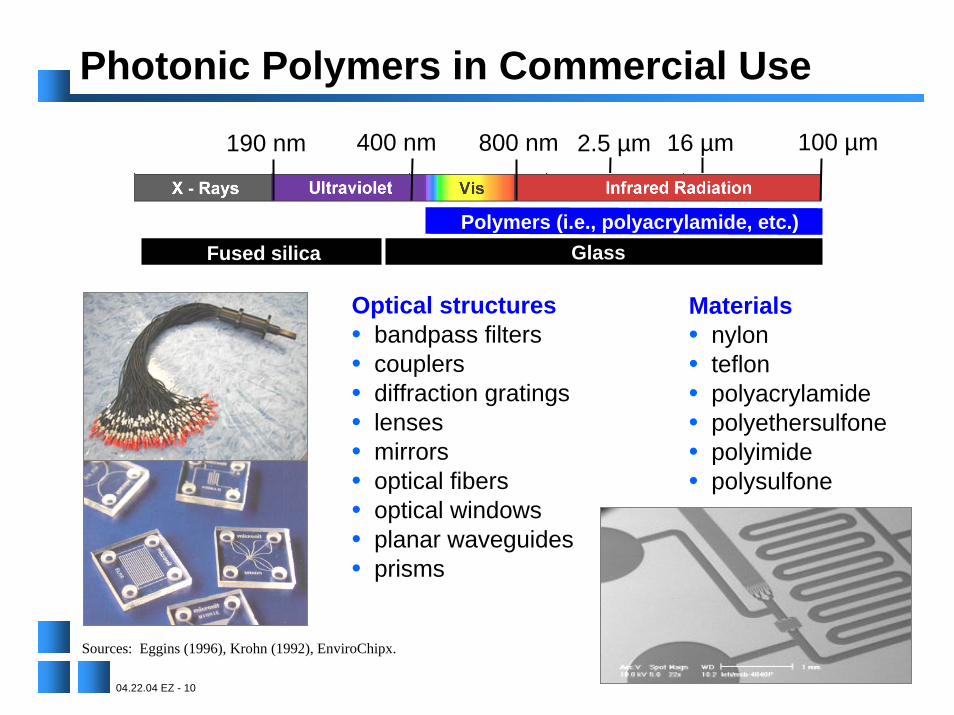
Photonic Polymers in Commercial Use
Sources: Eggins (1996), Krohn (1992), EnviroChipx.
04.22.04 EZ - 10
Optical structures • bandpass filters • couplers• diffraction gratings• lenses• mirrors• optical fibers• optical windows• planar waveguides• prisms
100 µm800 nm190 nm 2.5 µm400 nm 16 µm
Polymers (i.e., polyacrylamide, etc.)GlassFused silica
Materials• nylon• teflon• polyacrylamide• polyethersulfone• polyimide• polysulfone
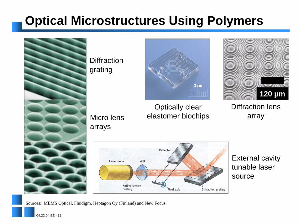
Optical Microstructures Using Polymers
120 µm
Diffractiongrating
Diffraction lens array
Optically clearelastomer biochipsMicro lens
arrays
External cavitytunable lasersource
Sources: MEMS Optical, Fluidigm, Heptagon Oy (Finland) and New Focus.
04.22.04 EZ - 11
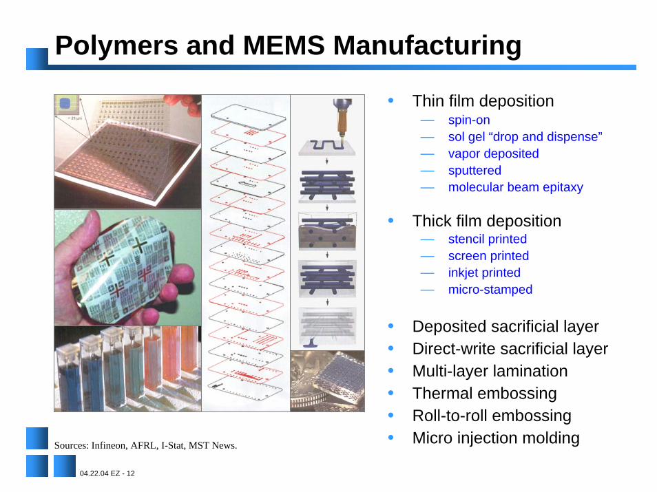
Polymers and MEMS Manufacturing
• Thin film deposition— spin-on— sol gel “drop and dispense”— vapor deposited— sputtered— molecular beam epitaxy
• Thick film deposition— stencil printed— screen printed— inkjet printed— micro-stamped
• Deposited sacrificial layer• Direct-write sacrificial layer• Multi-layer lamination• Thermal embossing• Roll-to-roll embossing• Micro injection moldingSources: Infineon, AFRL, I-Stat, MST News.
04.22.04 EZ - 12
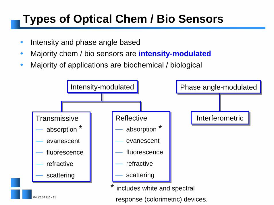
Types of Optical Chem / Bio Sensors
• Intensity and phase angle based• Majority chem / bio sensors are intensity-modulated• Majority of applications are biochemical / biological
Intensity-modulated
04.22.04 EZ - 13
Intensity-modulated
Transmissive— absorption *— evanescent
— fluorescence
— refractive
— scattering
Transmissive— absorption *— evanescent
— fluorescence
— refractive
— scattering
Phase angle-modulatedPhase angle-modulated
* includes white and spectral
response (colorimetric) devices.
Reflective— absorption *— evanescent
— fluorescence
— refractive
— scattering
Reflective— absorption *— evanescent
— fluorescence
— refractive
— scattering
InterferometricInterferometric
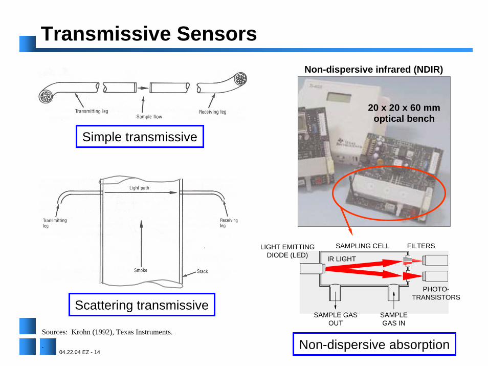
Transmissive Sensors
04.22.04 EZ - 14
Simple transmissive
PHOTO-TRANSISTORS
LIGHT EMITTINGDIODE (LED)
SAMPLING CELL
SAMPLE GAS OUT
SAMPLE GAS IN
FILTERS
IR LIGHT
Non-dispersive absorption
Non-dispersive infrared (NDIR)
Scattering transmissive
20 x 20 x 60 mmoptical bench
Sources: Krohn (1992), Texas Instruments.
.
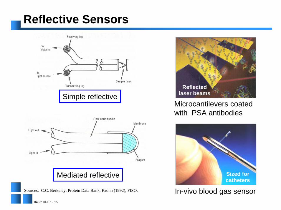
Reflective Sensors
Simple reflectiveReflected
laser beams
Microcantilevers coated with PSA antibodies
Mediated reflective Sized forcatheters
In-vivo blood gas sensorSources: C.C. Berkeley, Protein Data Bank, Krohn (1992), FISO.
04.22.04 EZ - 15
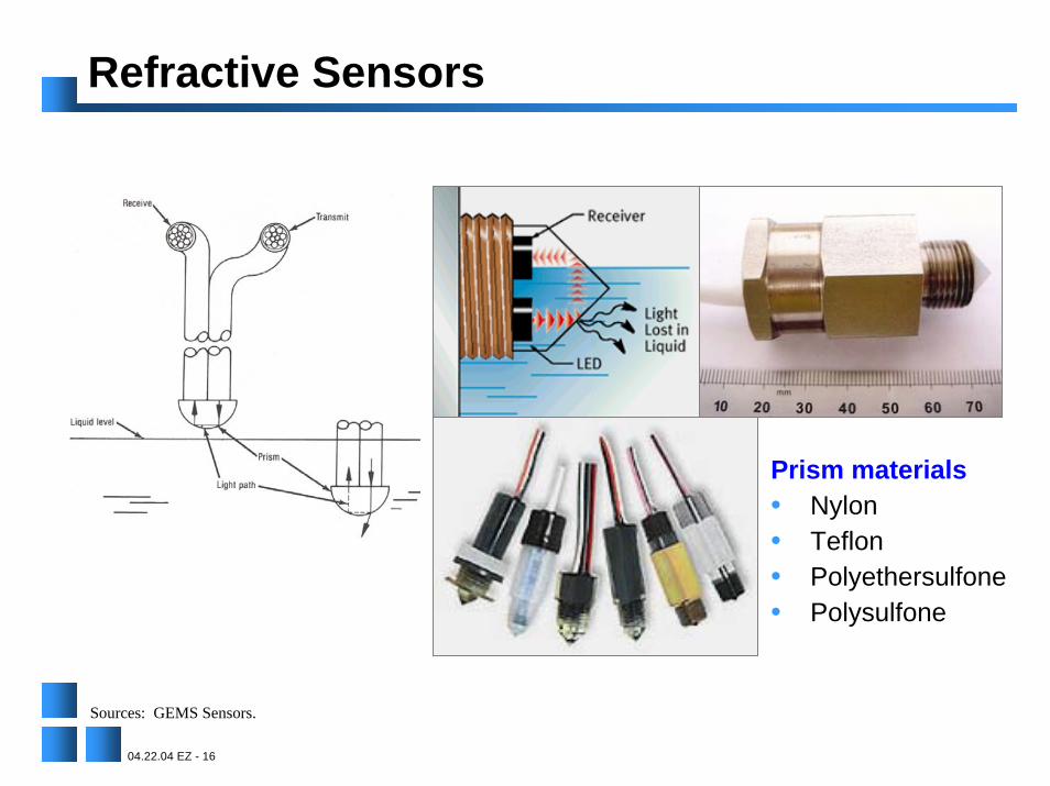
Refractive Sensors
Prism materials• Nylon • Teflon• Polyethersulfone• Polysulfone
Sources: GEMS Sensors.
04.22.04 EZ - 16
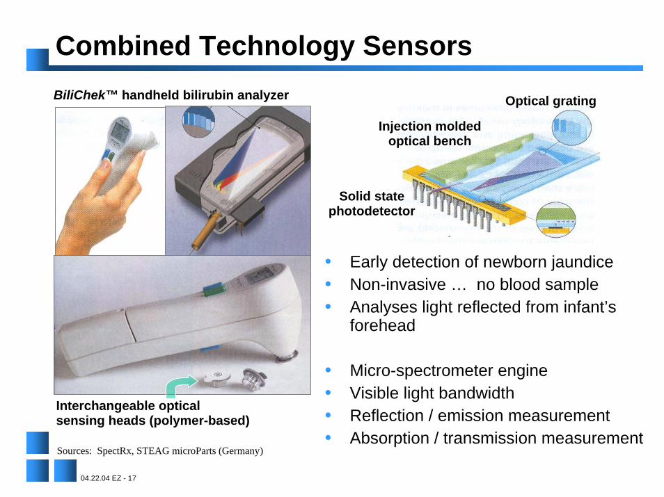
Combined Technology Sensors
04.22.04 EZ - 17
Sources: SpectRx, STEAG microParts (Germany)
• Early detection of newborn jaundice• Non-invasive … no blood sample• Analyses light reflected from infant’s
forehead
• Micro-spectrometer engine• Visible light bandwidth• Reflection / emission measurement• Absorption / transmission measurement
Optical grating
Interchangeable opticalsensing heads (polymer-based)
BiliChek™ handheld bilirubin analyzer
Injection moldedoptical bench
Solid statephotodetector
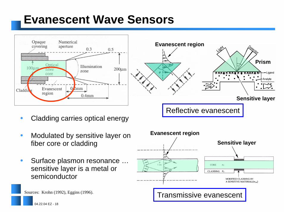
Evanescent Wave Sensors
• Cladding carries optical energy
• Modulated by sensitive layer on fiber core or cladding
• Surface plasmon resonance … sensitive layer is a metal or semiconductor
Evanescent region
Prism
Reflective evanescent
Evanescent region
Sensitive layer
Sensitive layer
Transmissive evanescentSources: Krohn (1992), Eggins (1996).
04.22.04 EZ - 18
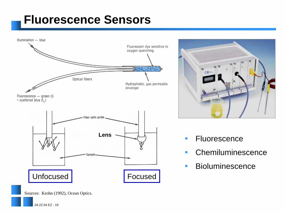
Fluorescence Sensors
Lens • Fluorescence
• Chemiluminescence
• BioluminescenceFocusedUnfocused
Sources: Krohn (1992), Ocean Optics.
04.22.04 EZ - 19
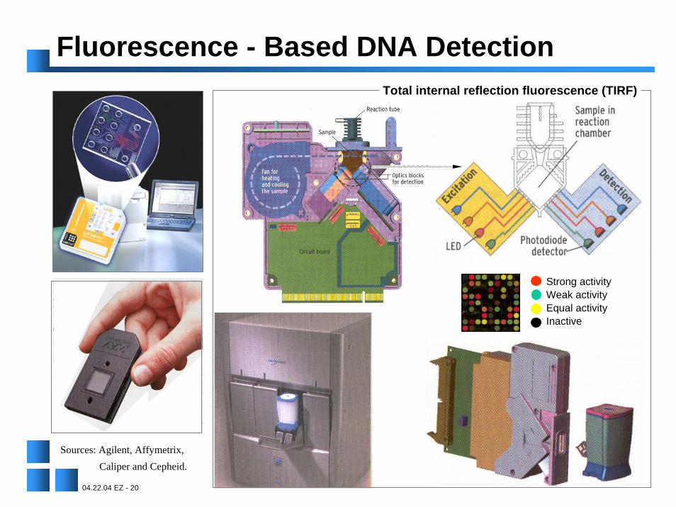
Fluorescence - Based DNA DetectionTotal internal reflection fluorescence (TIRF)
Strong activityWeak activityEqual activityInactive
Sources: Agilent, Affymetrix,Caliper and Cepheid.
04.22.04 EZ - 20
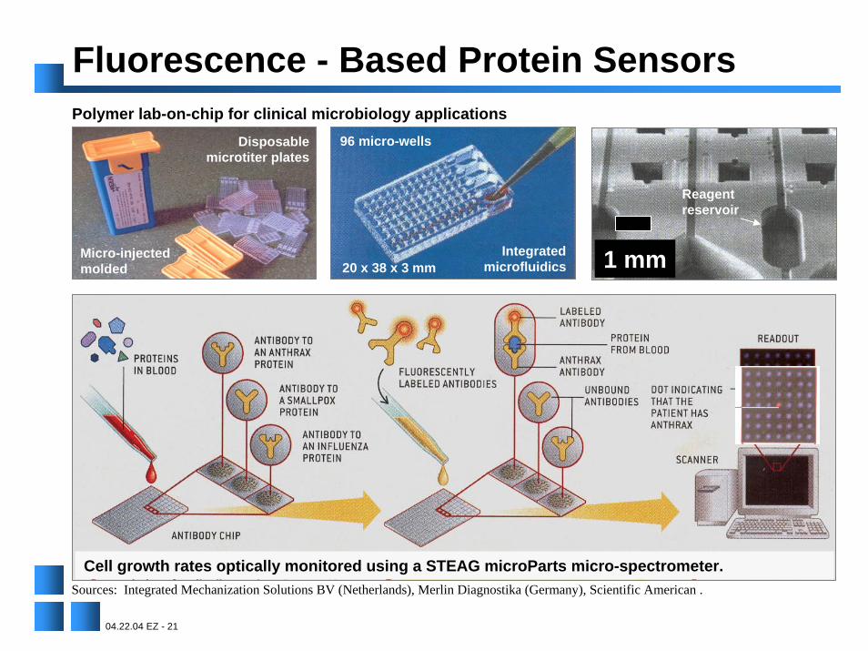
Fluorescence - Based Protein Sensors
1 mm
Disposable microtiter plates
Integratedmicrofluidics
Micro-injectedmolded
96 micro-wells
Reagentreservoir
20 x 38 x 3 mm
Polymer lab-on-chip for clinical microbiology applications
Sources: Integrated Mechanization Solutions BV (Netherlands), Merlin Diagnostika (Germany), Scientific American .
Cell growth rates optically monitored using a STEAG microParts micro-spectrometer.
04.22.04 EZ - 21
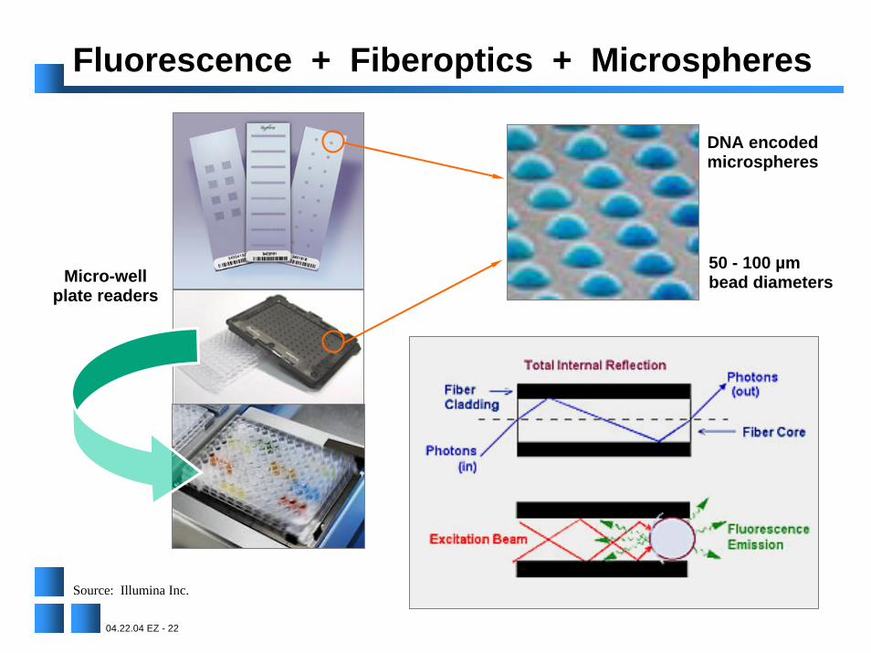
Fluorescence + Fiberoptics + Microspheres
DNA encodedmicrospheres
50 - 100 µmbead diameters Micro-well
plate readers
Source: Illumina Inc.
04.22.04 EZ - 22
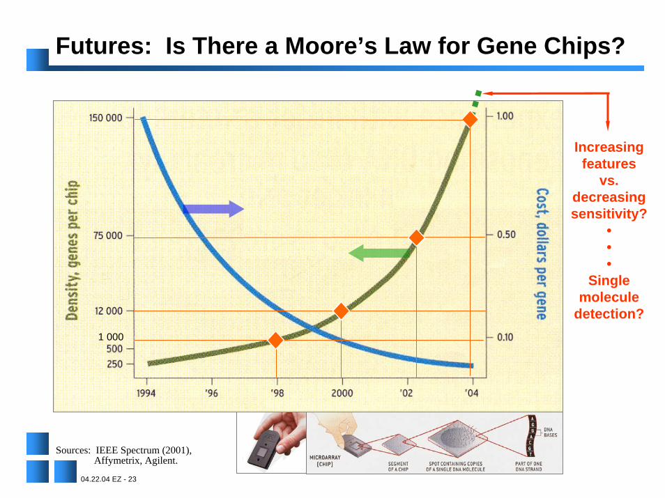
Futures: Is There a Moore’s Law for Gene Chips?
1 000
Increasingfeatures
vs.decreasingsensitivity?
•••
Singlemolecule
detection?
Sources: IEEE Spectrum (2001), Affymetrix, Agilent.
04.22.04 EZ - 23
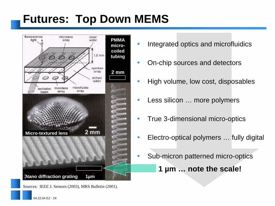
Futures: Top Down MEMS
• Integrated optics and microfluidics
• On-chip sources and detectors
• High volume, low cost, disposables
• Less silicon … more polymers
• True 3-dimensional micro-optics
• Electro-optical polymers … fully digital
• Sub-micron patterned micro-optics
1 µm … note the scale!
PMMAmicro-coiledtubing
2 mm
Micro-textured lens
Nano diffraction grating 1µm
Sources: IEEE J. Sensors (2003), MRS Bulletin (2001).
04.22.04 EZ - 24
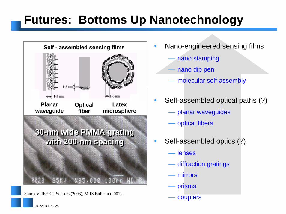
Futures: Bottoms Up Nanotechnology
• Nano-engineered sensing films— nano stamping
— nano dip pen
— molecular self-assembly
• Self-assembled optical paths (?)— planar waveguides
— optical fibers
• Self-assembled optics (?)— lenses
— diffraction gratings
— mirrors
— prisms
Planarwaveguide
Opticalfiber
Latexmicrosphere
30-nm wide PMMA gratingwith 200-nm spacing
30-nm wide PMMA gratingwith 200-nm spacing
Self - assembled sensing films
Sources: IEEE J. Sensors (2003), MRS Bulletin (2001). — couplers04.22.04 EZ - 25
Microsystems for Life ™
Contacts:
Ed ZdankiewiczCEO and CTO
EnviroChipx LLC
Tel: (216) 374 - 3377
Email: [email protected]
Terry MartellCOO and CFO
EnviroChipx LLC
Tel: (330) 655 - 2238
Email: [email protected]
04.22.04 EZ - 26


![Temperature Sensing Polymer, [Au(+I)(p-SPhCO H)] , for … · 2017. 9. 13. · S1 Electronic Supporting Information for: Intrinsic Dual-Emitting Gold Thiolate Coordination Polymer,](https://img.pdfslide.us/doc/110x75/60e9e75d195a95200162eb20/temperature-sensing-polymer-auip-sphco-h-for-2017-9-13-s1-electronic.jpg)