Embed Size (px)
Citation preview
David Muller
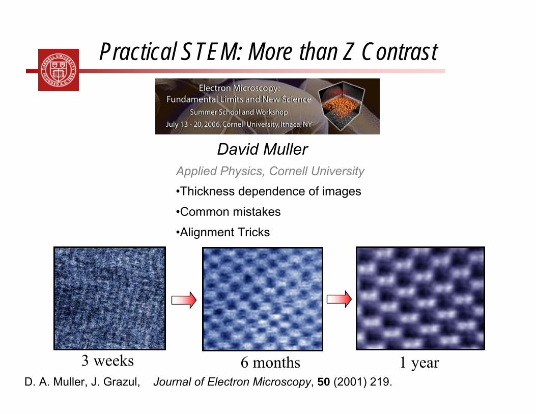
Practical STEM: More than Z Contrast
Applied Physics, Cornell University•Thickness dependence of images
•Common mistakes
•Alignment Tricks
6 months3 weeks 1 yearD. A. Muller, J. Grazul, Journal of Electron Microscopy, 50 (2001) 219.
Matt Weyland, Zhiheng Yu, Peter Ercius, Lena Fitting, Earl Kirkland
Applied Physics, Cornell University
Acknowledgements
Paul VoylesUniversity of Wisconsin, Madison
John Grazul, Mick ThomasCornell Center for Materials Research
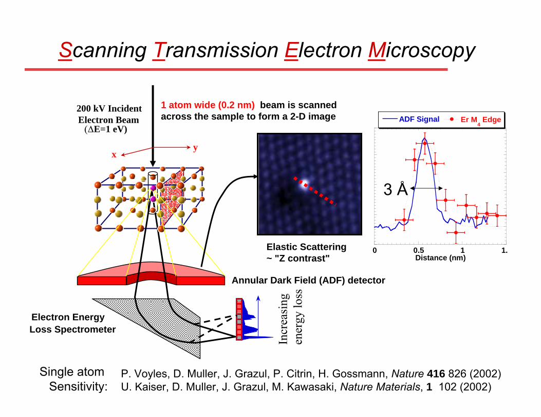
Single atom Sensitivity:
Electron Energy Loss Spectrometer
Annular Dark Field (ADF) detector
yx
200 kV IncidentElectron Beam (∆E=1 eV)
Incr
easi
ngen
ergy
loss
1 atom wide (0.2 nm) beam is scannedacross the sample to form a 2-D image
Elastic Scattering ~ "Z contrast"
Scanning Transmission Electron Microscopy
0 0.5 1 1.
ADF Signal Er M4 Edge
Distance (nm)
3 Å
P. Voyles, D. Muller, J. Grazul, P. Citrin, H. Gossmann, Nature 416 826 (2002)U. Kaiser, D. Muller, J. Grazul, M. Kawasaki, Nature Materials, 1 102 (2002)
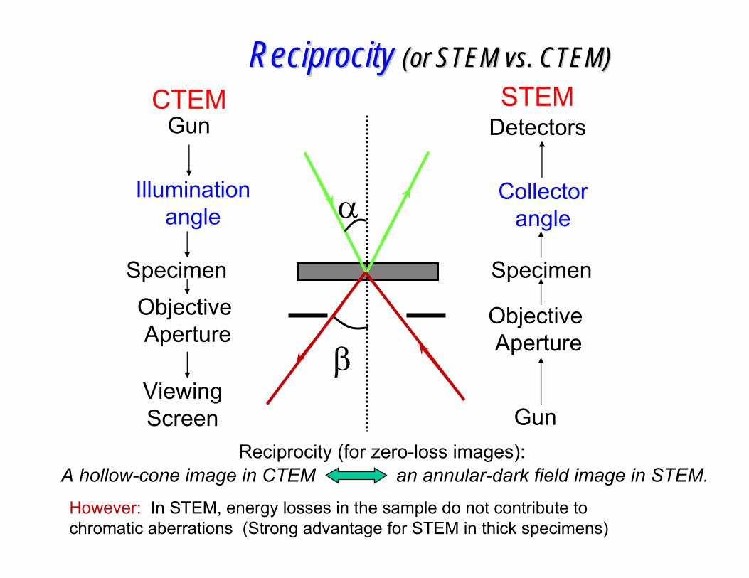
ReciprocityReciprocity (or STEM vs. CTEM)(or STEM vs. CTEM)CTEM STEM
Reciprocity (for zero-loss images):A hollow-cone image in CTEM an annular-dark field image in STEM.
Specimen
Illuminationangle α Collector
angle
β
Specimen
Objective Aperture
Objective Aperture
ViewingScreen Gun
Gun Detectors
However: In STEM, energy losses in the sample do not contribute to chromatic aberrations (Strong advantage for STEM in thick specimens)
David Muller 2006 5
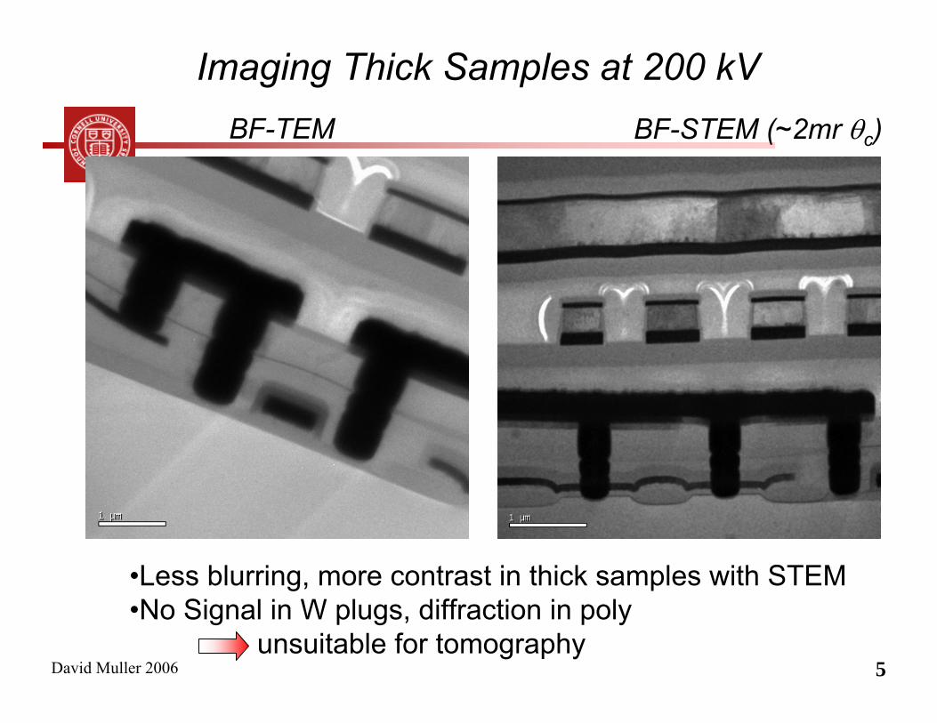
Imaging Thick Samples at 200 kVBF-TEM BF-STEM (~2mr θc)
•Less blurring, more contrast in thick samples with STEM•No Signal in W plugs, diffraction in poly
unsuitable for tomography
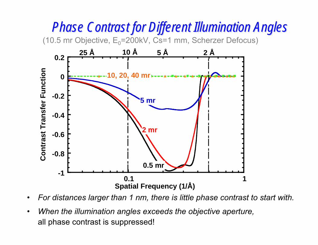
Phase Contrast for Different Illumination AnglesPhase Contrast for Different Illumination Angles
• For distances larger than 1 nm, there is little phase contrast to start with.
• When the illumination angles exceeds the objective aperture,all phase contrast is suppressed!
-1
-0.8
-0.6
-0.4
-0.2
0
0.2
0.1 1
Con
tras
t Tra
nsfe
r Fun
ctio
n
Spatial Frequency (1/Å)
0.5 mr
2 mr
5 mr
10, 20, 40 mr
25 Å 5 Å 2 Å10 Å(10.5 mr Objective, E0=200kV, Cs=1 mm, Scherzer Defocus)
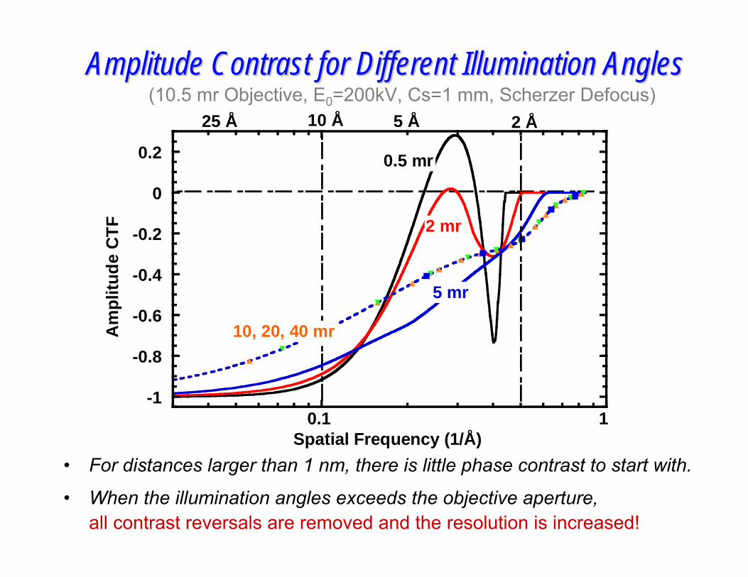
Amplitude Contrast for Different Illumination AnglesAmplitude Contrast for Different Illumination Angles
• For distances larger than 1 nm, there is little phase contrast to start with.
• When the illumination angles exceeds the objective aperture,all contrast reversals are removed and the resolution is increased!
(10.5 mr Objective, E0=200kV, Cs=1 mm, Scherzer Defocus)
-1
-0.8
-0.6
-0.4
-0.2
0
0.2
0.1 1
Am
plitu
de C
TF
0.5 mr
2 mr
5 mr
10, 20, 40 mr
25 Å 5 Å 2 Å10 Å
Spatial Frequency (1/Å)
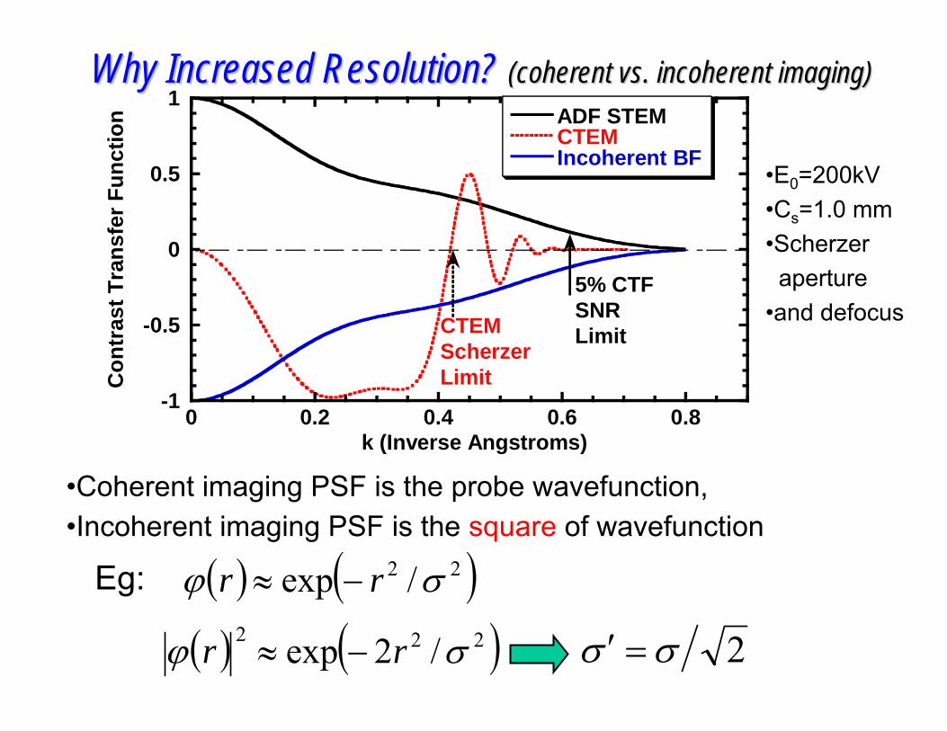
Why Increased Resolution? Why Increased Resolution? (coherent vs. incoherent imaging)(coherent vs. incoherent imaging)
-1
-0.5
0
0.5
1
0 0.2 0.4 0.6 0.8
ADF STEMCTEMIncoherent BF
Con
tras
t Tra
nsfe
r Fun
ctio
n
k (Inverse Angstroms)
CTEM Scherzer Limit
5% CTFSNRLimit
•E0=200kV•Cs=1.0 mm•Scherzeraperture
•and defocus
( ) ( )22 /exp σϕ rr −≈Eg:
•Coherent imaging PSF is the probe wavefunction,•Incoherent imaging PSF is the square of wavefunction
( ) ( )222 /2exp σϕ rr −≈ 2σσ =′
David Muller 2006 9
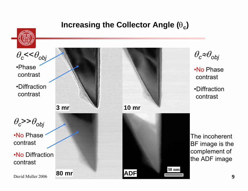
Increasing the Collector Angle (θc)
1 2
3 430 nm
3 mr 10 mr
80 mr ADF
θc>>θobj
•No Phasecontrast
•No Diffractioncontrast
θc<<θobj•Phasecontrast
•Diffractioncontrast
θc≈θobj
•No Phasecontrast
•Diffractioncontrast
The incoherent BF image is the complement of the ADF image
David Muller 2006 10
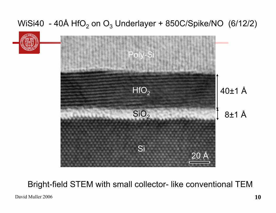
WiSi40 - 40Å HfO2 on O3 Underlayer + 850C/Spike/NO (6/12/2)
8±1 Å
Si
Poly-Si
HfO2
SiO2
40±1 Å
Bright-field STEM with small collector- like conventional TEM
20 Å
David Muller 2006 11
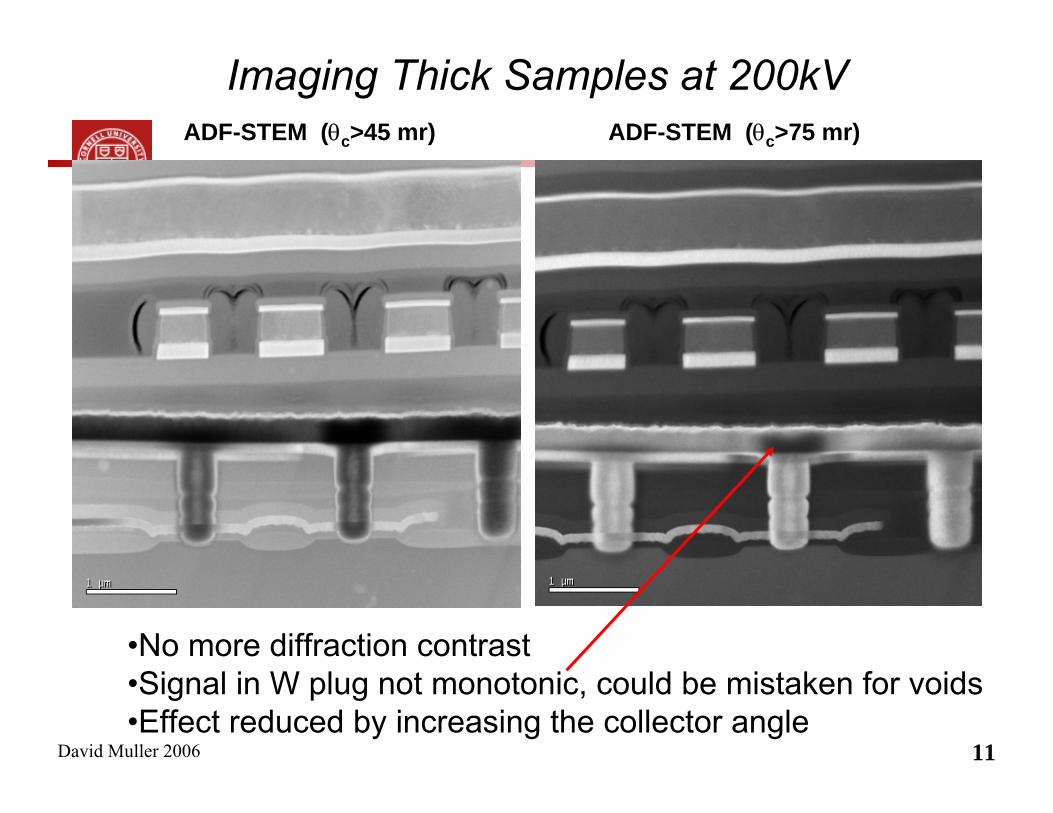
Imaging Thick Samples at 200kVADF-STEM (θc>45 mr) ADF-STEM (θc>75 mr)
•No more diffraction contrast•Signal in W plug not monotonic, could be mistaken for voids•Effect reduced by increasing the collector angle
David Muller 2006 12
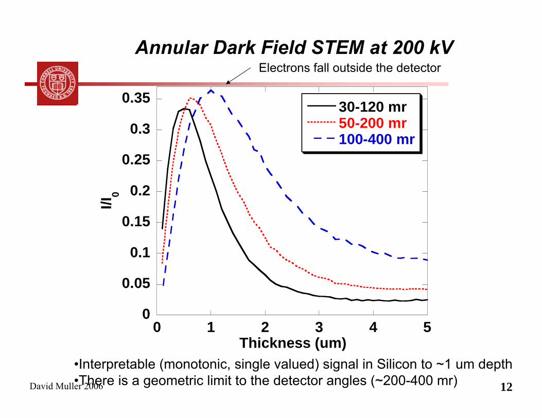
Annular Dark Field STEM at 200 kV
•Interpretable (monotonic, single valued) signal in Silicon to ~1 um depth•There is a geometric limit to the detector angles (~200-400 mr)
0
0.05
0.1
0.15
0.2
0.25
0.3
0.35
0 1 2 3 4 5
30-120 mr50-200 mr100-400 mr
I/I0
Thickness (um)
Electrons fall outside the detector
David Muller 2006 13
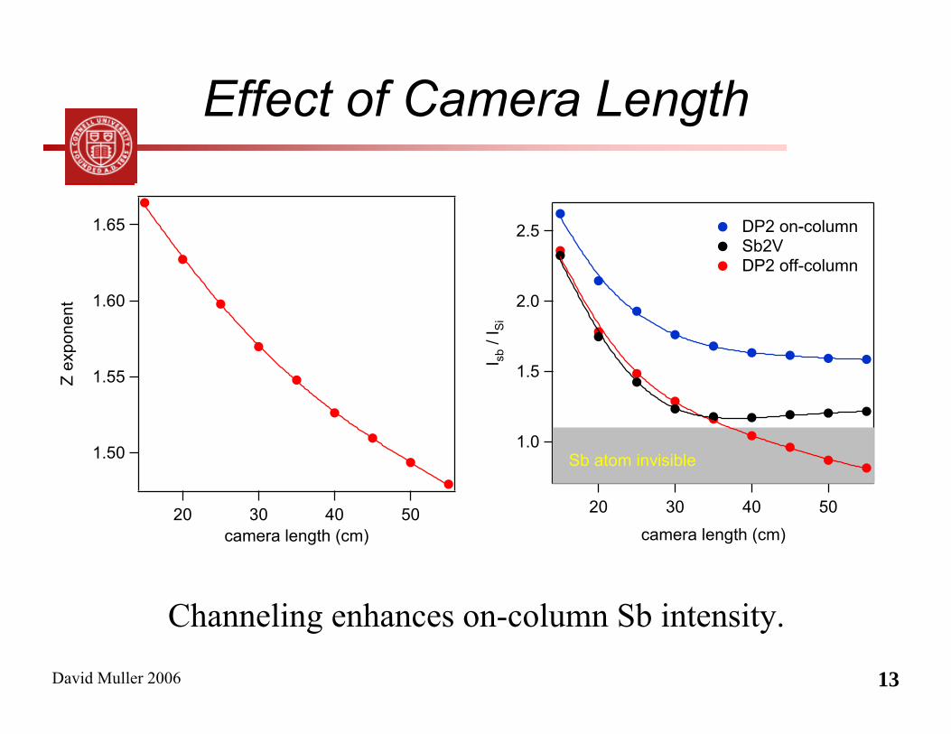
Effect of Camera Length
1.65
1.60
1.55
1.50
Z ex
pone
nt
50403020camera length (cm)
2.5
2.0
1.5
1.0
I sb /
I Si
50403020camera length (cm)
Sb atom invisible
DP2 on-column Sb2V DP2 off-column
Channeling enhances on-column Sb intensity.
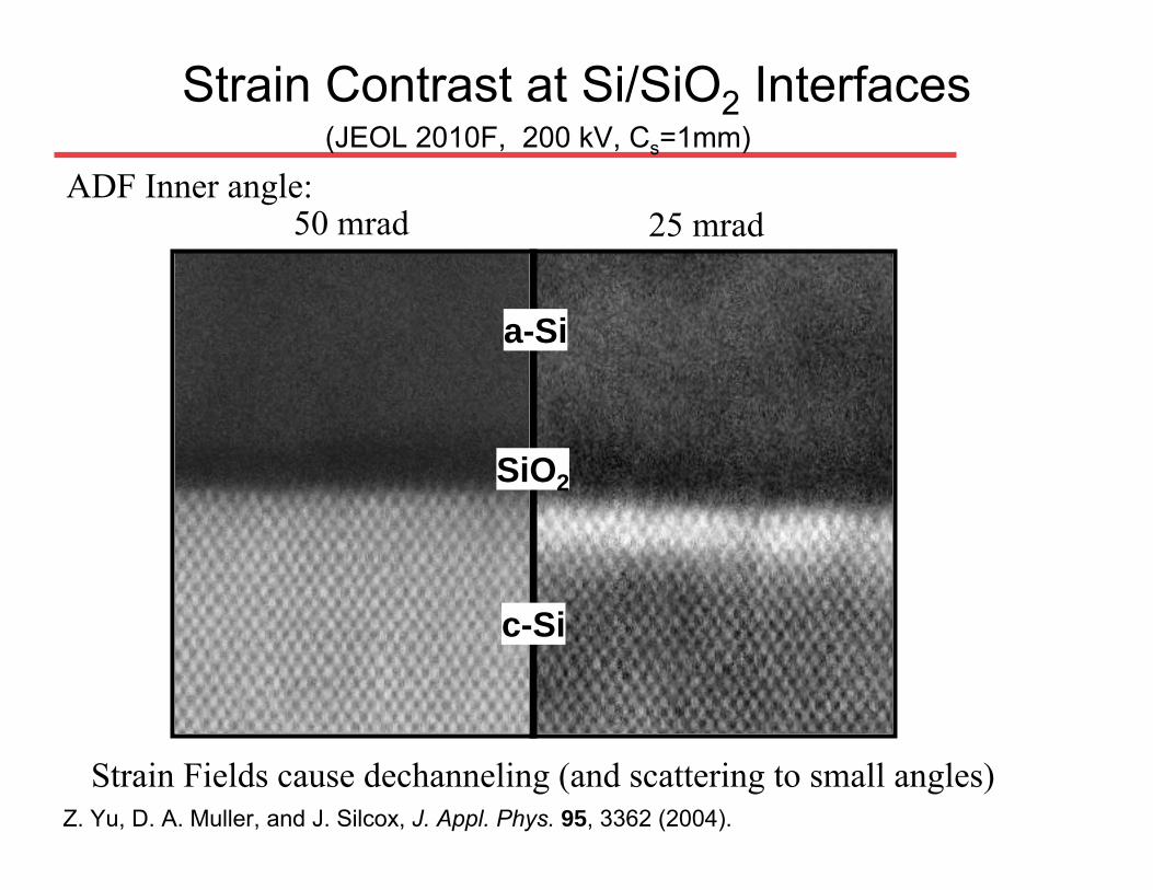
Strain Contrast at Si/SiO2 Interfaces
David Muller 2001
50 mrad 25 mrad
c-Si
SiO2
a-Si
(JEOL 2010F, 200 kV, Cs=1mm)
Strain Fields cause dechanneling (and scattering to small angles)
ADF Inner angle:
Z. Yu, D. A. Muller, and J. Silcox, J. Appl. Phys. 95, 3362 (2004).
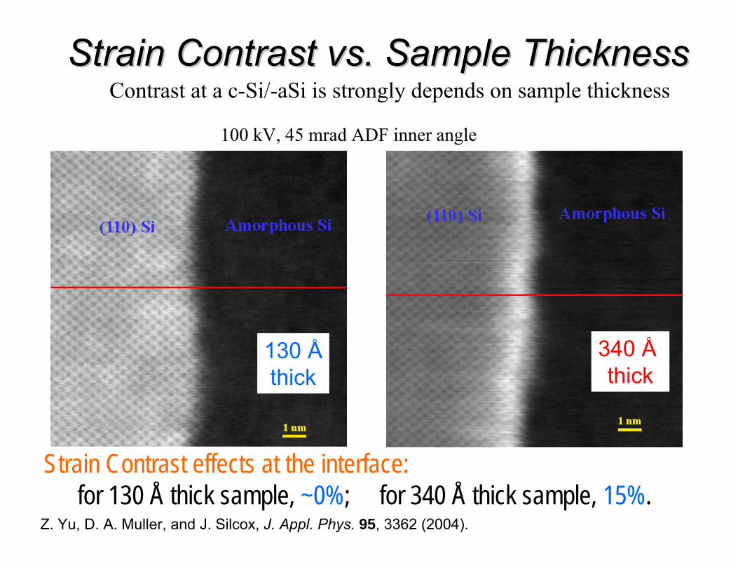
Strain Contrast vs. Sample ThicknessStrain Contrast vs. Sample ThicknessContrast at a c-Si/-aSi is strongly depends on sample thickness
130 Åthick
340 Åthick
Strain Contrast effects at the interface:for 130 Å thick sample, ~0%; for 340 Å thick sample, 15%.
100 kV, 45 mrad ADF inner angle
Z. Yu, D. A. Muller, and J. Silcox, J. Appl. Phys. 95, 3362 (2004).
David Muller 2006 16
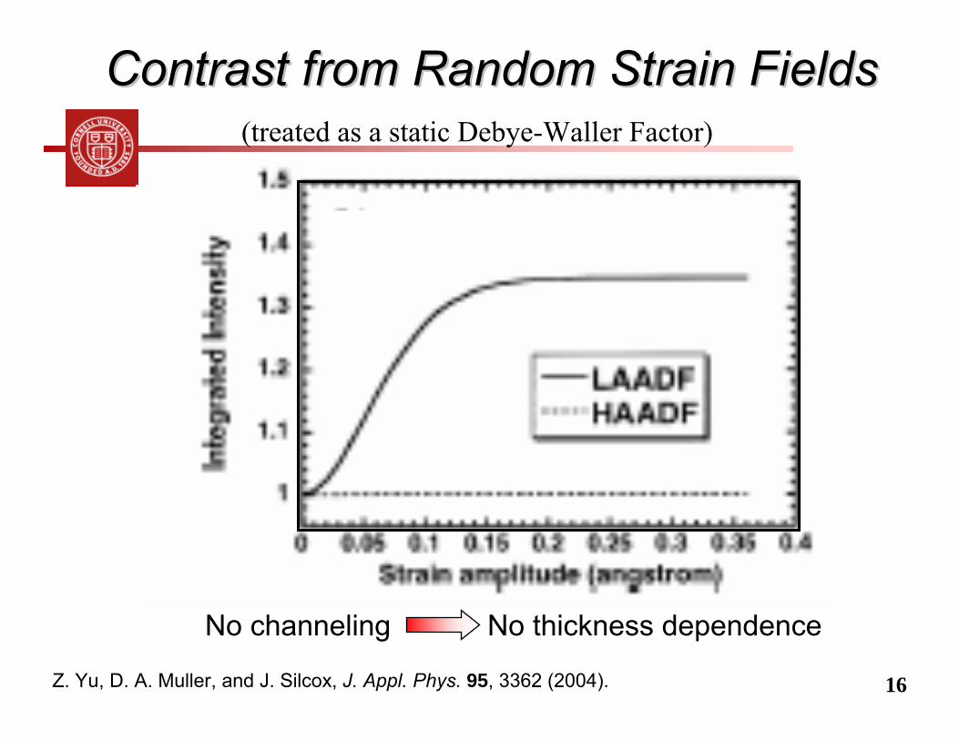
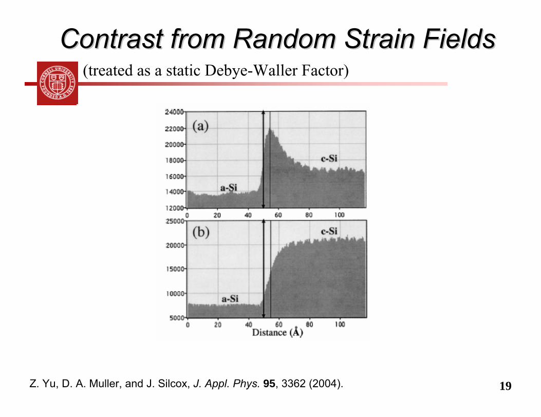
Contrast from Random Strain FieldsContrast from Random Strain Fields(treated as a static Debye-Waller Factor)
No channeling No thickness dependence
Z. Yu, D. A. Muller, and J. Silcox, J. Appl. Phys. 95, 3362 (2004).
David Muller 2006 17
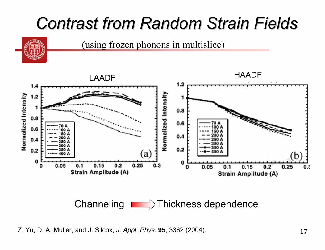
Contrast from Random Strain FieldsContrast from Random Strain Fields(using frozen phonons in multislice)
Channeling Thickness dependence
LAADF HAADF
Z. Yu, D. A. Muller, and J. Silcox, J. Appl. Phys. 95, 3362 (2004).
David Muller 2006 18
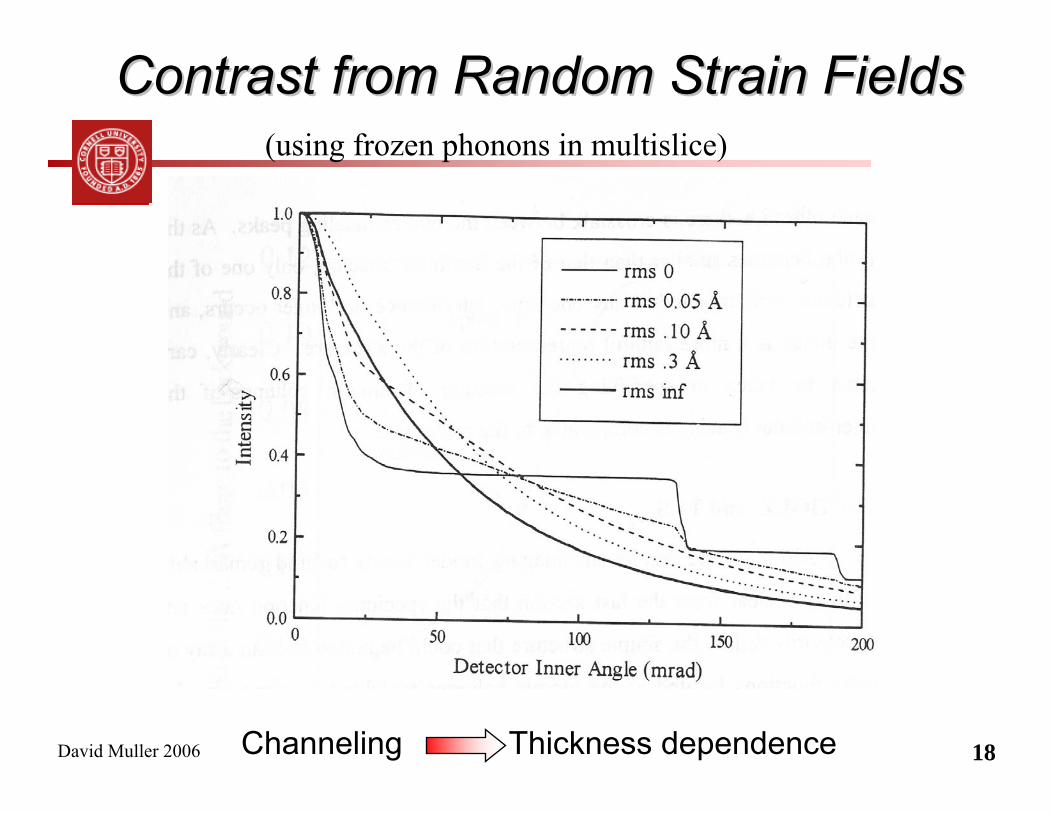
Contrast from Random Strain FieldsContrast from Random Strain Fields(using frozen phonons in multislice)
Channeling Thickness dependence
David Muller 2006 19
Contrast from Random Strain FieldsContrast from Random Strain Fields(treated as a static Debye-Waller Factor)
Z. Yu, D. A. Muller, and J. Silcox, J. Appl. Phys. 95, 3362 (2004).
David Muller 2006 20
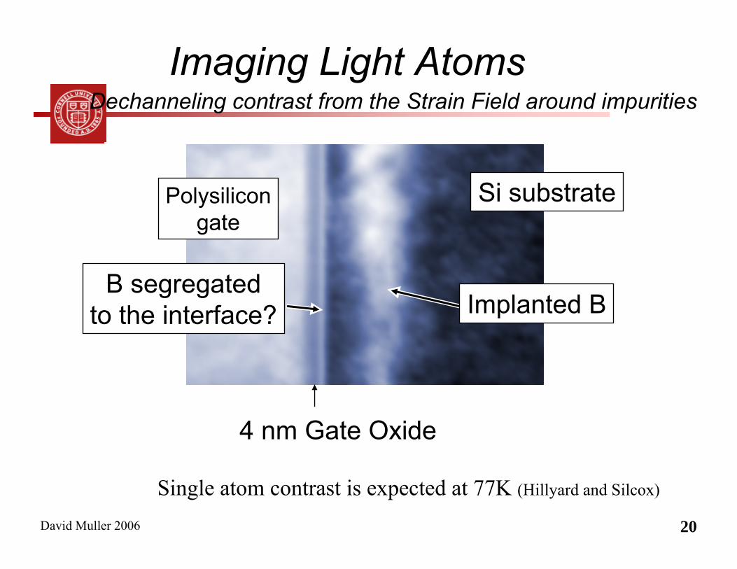
Imaging Light AtomsDechanneling contrast from the Strain Field around impurities
Si substrate
4 nm Gate Oxide
Polysilicongate
Implanted BB segregated
to the interface?
Single atom contrast is expected at 77K (Hillyard and Silcox)
David Muller 2006 21
1
1.5
2
-5 0 5 10LA
AD
F C
ontr
ast
Distance (nm)
La Markersubstrate
0
0.5
1
-5 0 5 10
Ti3+
La
Frac
tion
Distance (nm)
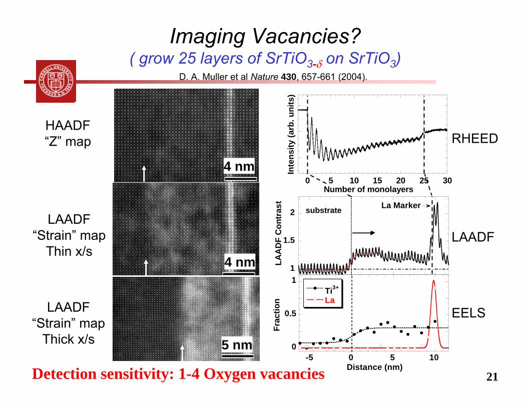
Imaging Vacancies?( grow 25 layers of SrTiO3-δ on SrTiO3)
HAADF “Z” map
LAADF “Strain” map
Thin x/s
0 5 10 15 20 25 30
Inte
nsity
(arb
. uni
ts)
Number of monolayers
RHEED
LAADF
EELS
4 nm
4 nm
5 nm
LAADF “Strain” map
Thick x/s
Detection sensitivity: 1-4 Oxygen vacancies
D. A. Muller et al Nature 430, 657-661 (2004).
David Muller 2006 22
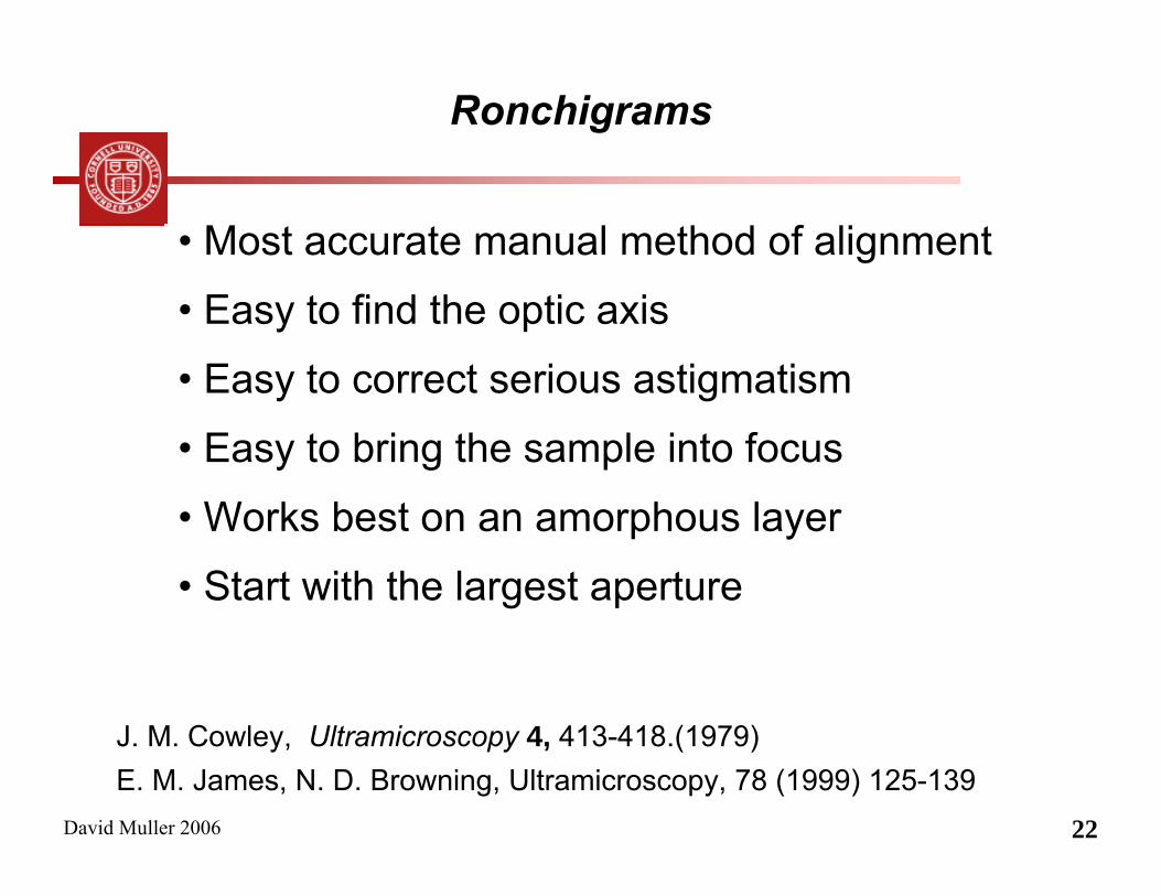
Ronchigrams
• Most accurate manual method of alignment
• Easy to find the optic axis
• Easy to correct serious astigmatism
• Easy to bring the sample into focus
• Works best on an amorphous layer
• Start with the largest aperture
E. M. James, N. D. Browning, Ultramicroscopy, 78 (1999) 125-139 J. M. Cowley, Ultramicroscopy 4, 413-418.(1979)
David Muller 2006 23
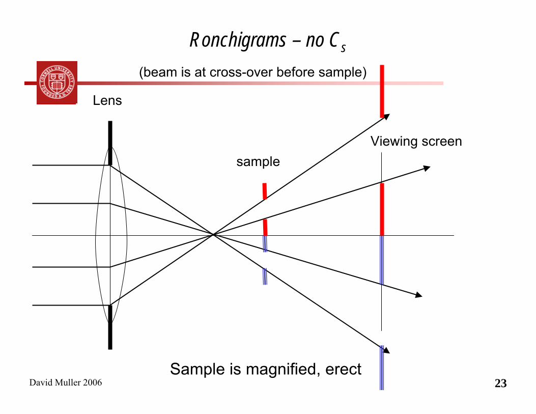
Ronchigrams – no Cs
Lens
sampleViewing screen
(beam is at cross-over before sample)
Sample is magnified, erect
David Muller 2006 24
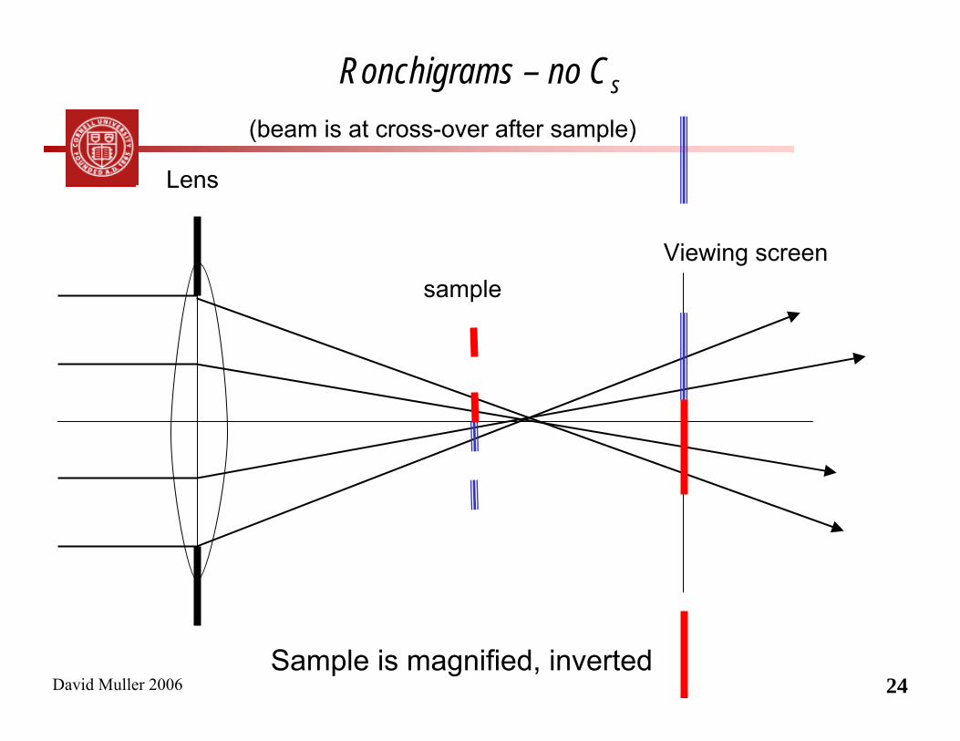
Ronchigrams – no Cs
Lens
sampleViewing screen
(beam is at cross-over after sample)
Sample is magnified, inverted
David Muller 2006 25
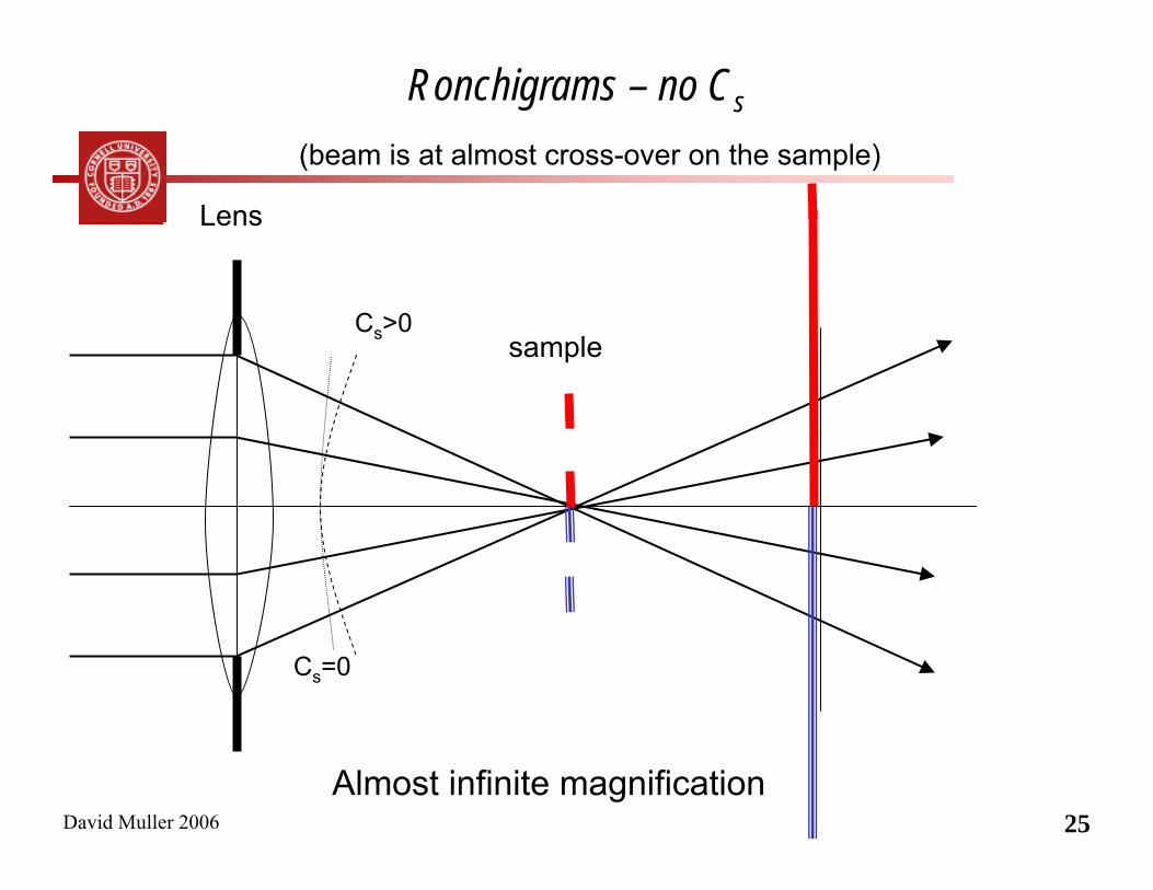
Lens
Cs=0
Cs>0sample
Ronchigrams – no Cs
(beam is at almost cross-over on the sample)
Almost infinite magnification
David Muller 2006 26
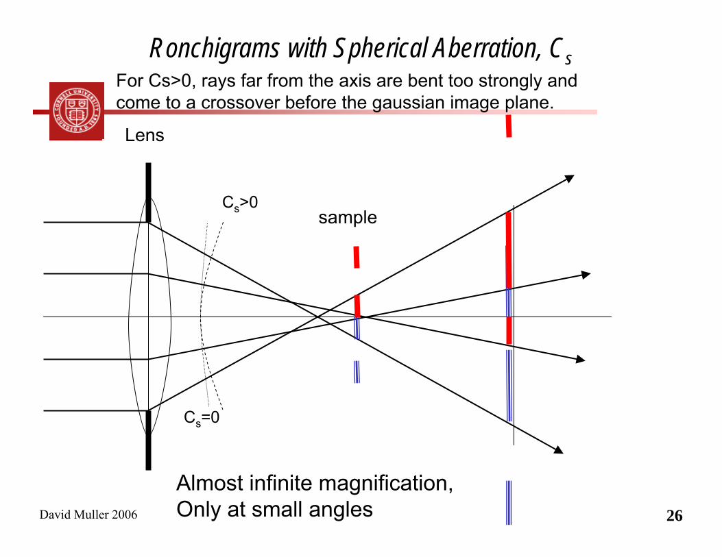
Ronchigrams with Spherical Aberration, Cs
Lens
Cs=0
Cs>0sample
For Cs>0, rays far from the axis are bent too strongly and come to a crossover before the gaussian image plane.
Almost infinite magnification,Only at small angles
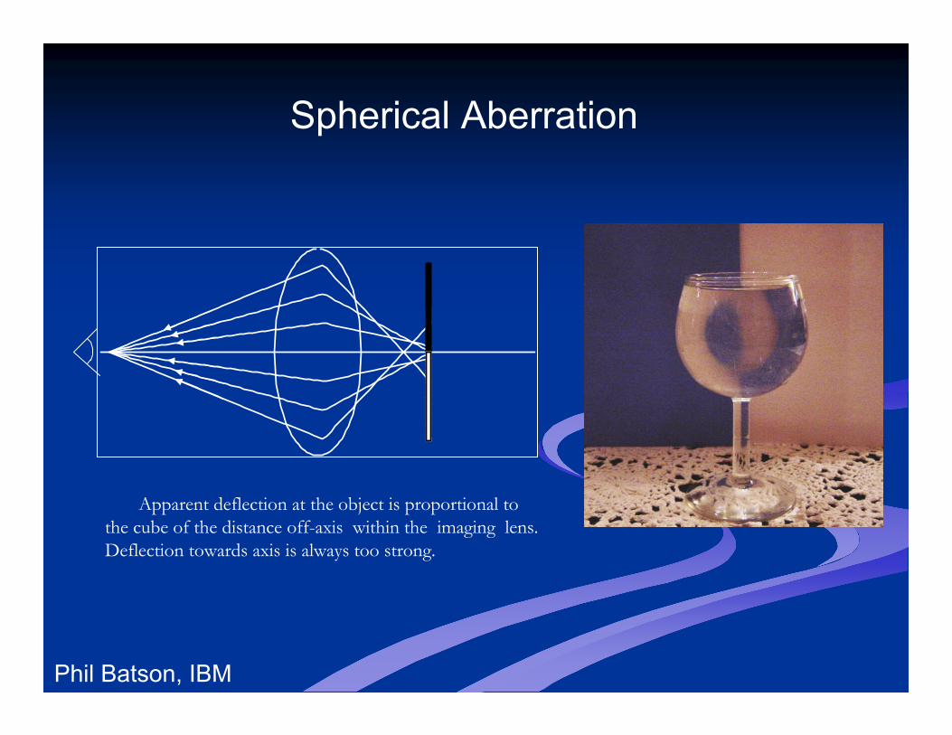
Spherical Aberration
Apparent deflection at the object is proportional tothe cube of the distance off-axis within the imaging lens. Deflection towards axis is always too strong.
Phil Batson, IBM

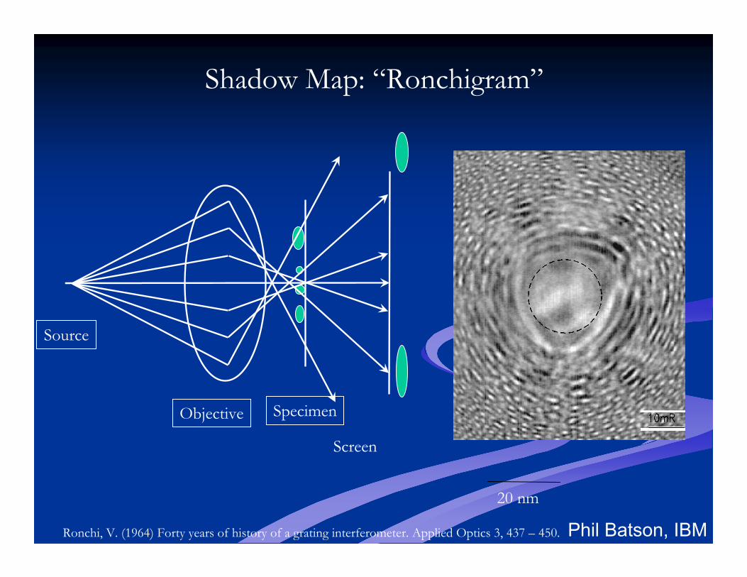
Screen
Specimen
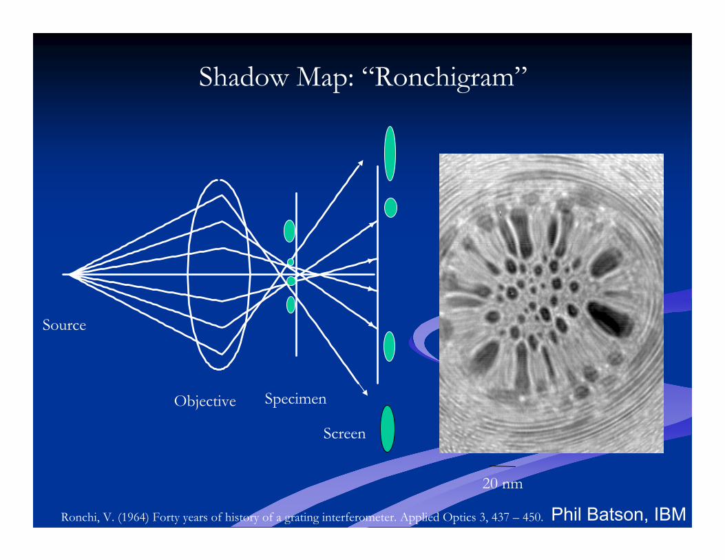
Shadow Map: “Ronchigram”
Objective
20 nm
Source
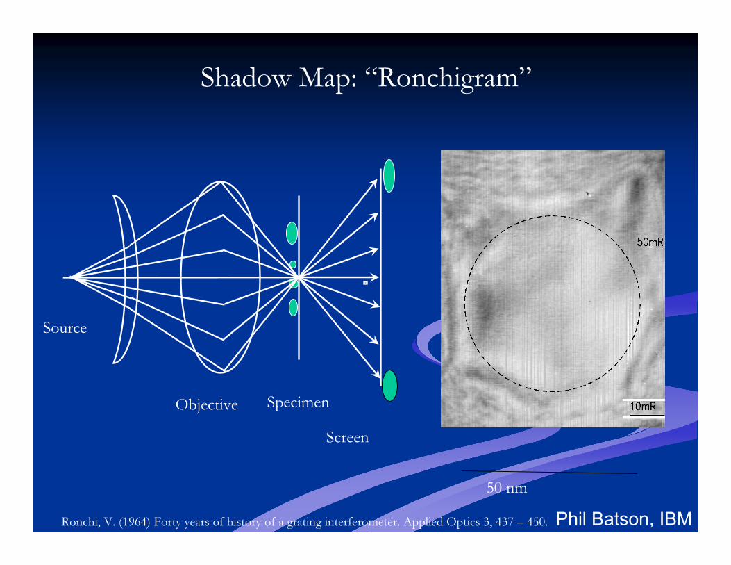
Ronchi, V. (1964) Forty years of history of a grating interferometer. Applied Optics 3, 437 – 450. Phil Batson, IBM
Screen
Specimen
Shadow Map: “Ronchigram”
Objective
20 nm
Source
Ronchi, V. (1964) Forty years of history of a grating interferometer. Applied Optics 3, 437 – 450. Phil Batson, IBM
Screen
Specimen
Shadow Map: “Ronchigram”
Objective
20 nm
Source
Ronchi, V. (1964) Forty years of history of a grating interferometer. Applied Optics 3, 437 – 450. Phil Batson, IBM
Screen
Specimen
Shadow Map: “Ronchigram”
Objective
20 nm
Source
Ronchi, V. (1964) Forty years of history of a grating interferometer. Applied Optics 3, 437 – 450. Phil Batson, IBM
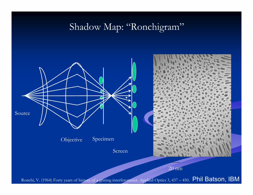
Screen
Specimen
Shadow Map: “Ronchigram”
Objective
50 nm
Source
Ronchi, V. (1964) Forty years of history of a grating interferometer. Applied Optics 3, 437 – 450. Phil Batson, IBM
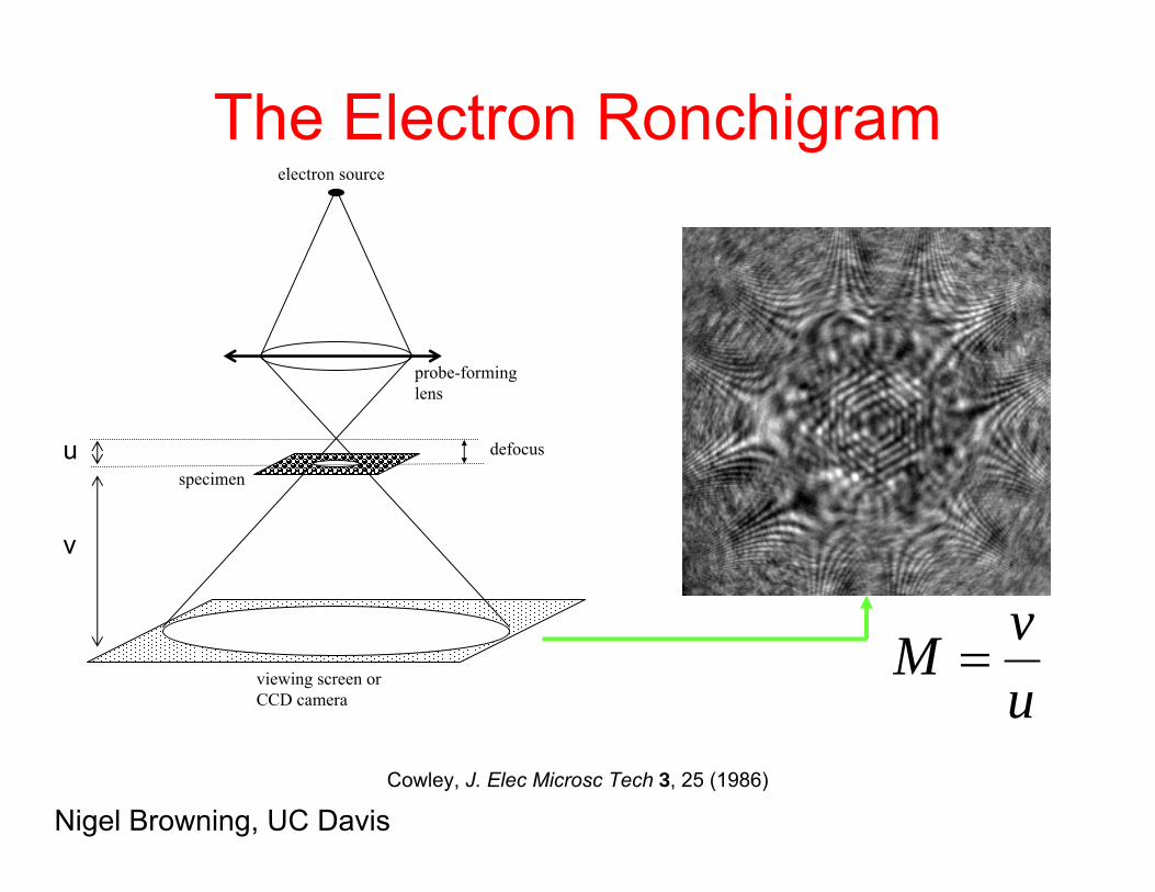
viewing screen or CCD camera
specimen
electron source
probe-forming lens
defocus
The Electron Ronchigram
Cowley, J. Elec Microsc Tech 3, 25 (1986)
u
v
uvM =
Nigel Browning, UC Davis
David Muller 2006 34
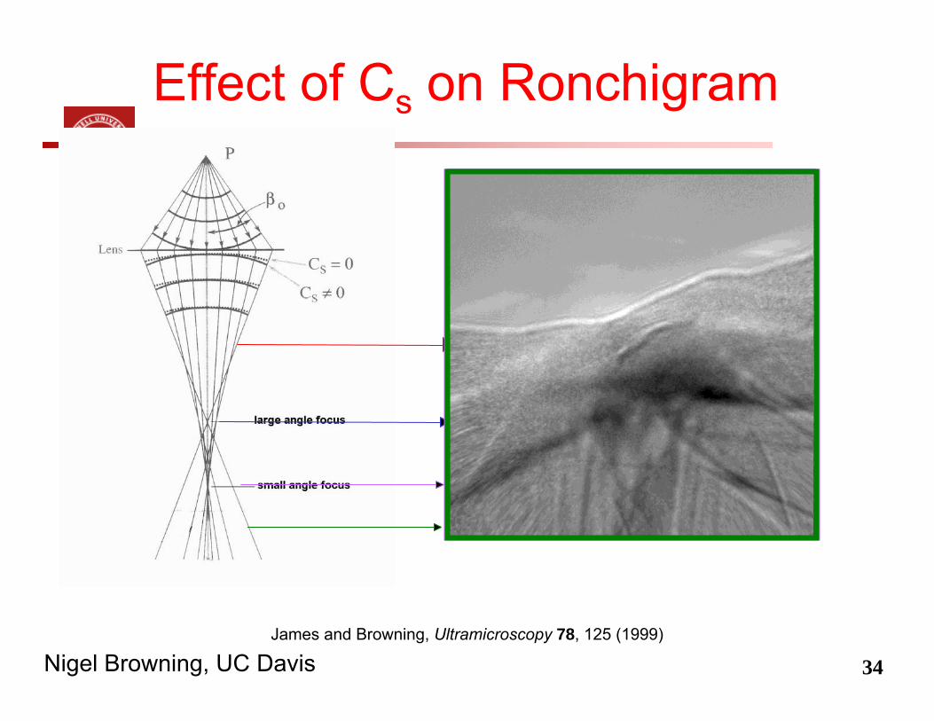
Effect of Cs on Ronchigram
James and Browning, Ultramicroscopy 78, 125 (1999)
Nigel Browning, UC Davis
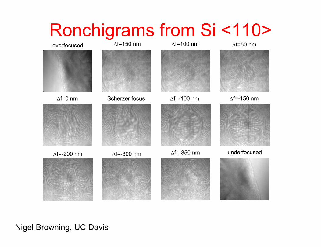
Ronchigrams from Si <110>overfocused
underfocused
∆f=0 nm Scherzer focus ∆f=-100 nm ∆f=-150 nm
∆f=-200 nm ∆f=-300 nm ∆f=-350 nm
∆f=100 nm ∆f=50 nm∆f=150 nm
Nigel Browning, UC Davis
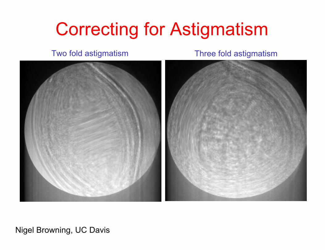
Two fold astigmatism Three fold astigmatism
Correcting for Astigmatism
Nigel Browning, UC Davis
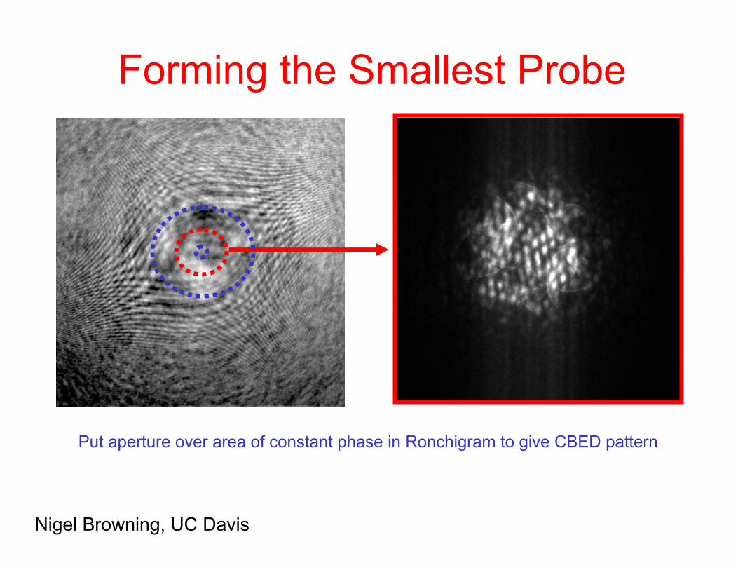
Forming the Smallest Probe
Put aperture over area of constant phase in Ronchigram to give CBED pattern
Nigel Browning, UC Davis
David Muller 2006 38
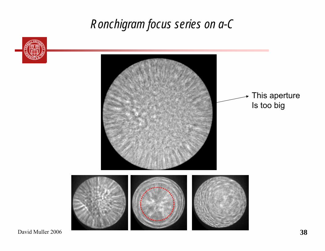
Ronchigram focus series on a-C
This apertureIs too big
David Muller 2006 39
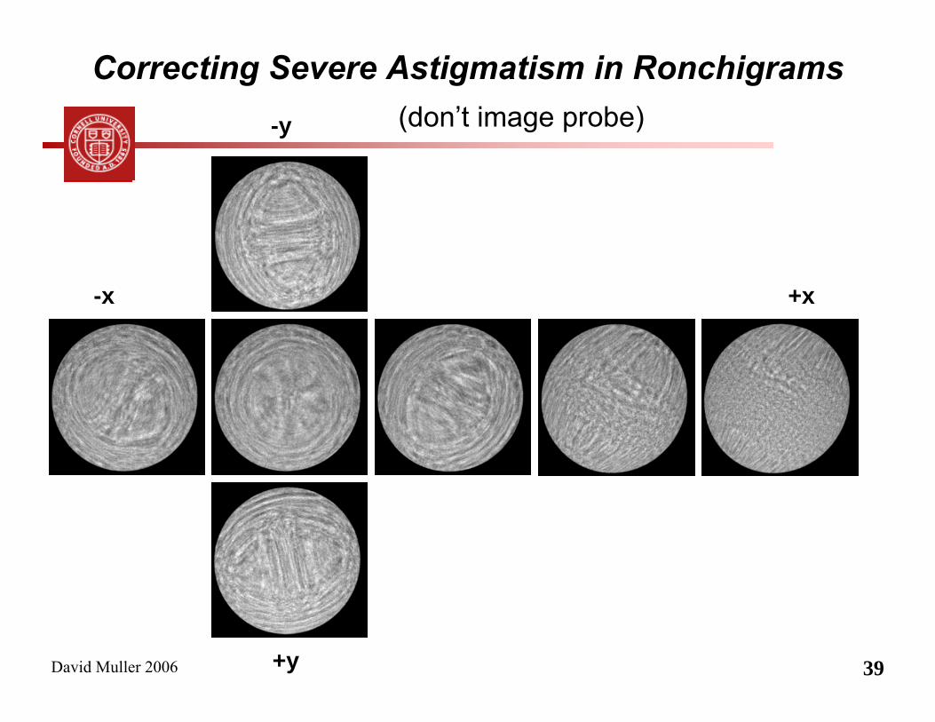
Correcting Severe Astigmatism in Ronchigrams
+y
-y
+x-x
(don’t image probe)
David Muller 2006 40
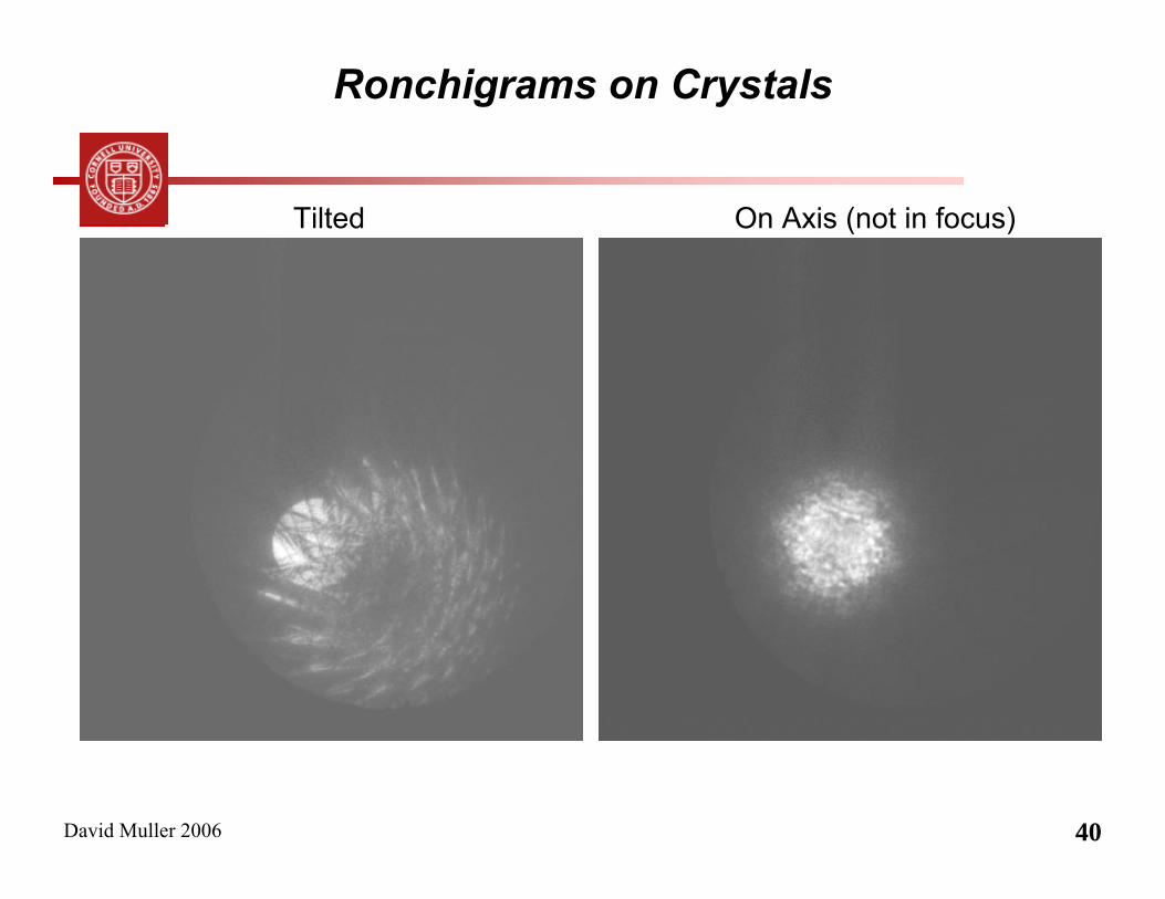
Ronchigrams on Crystals
Tilted On Axis (not in focus)
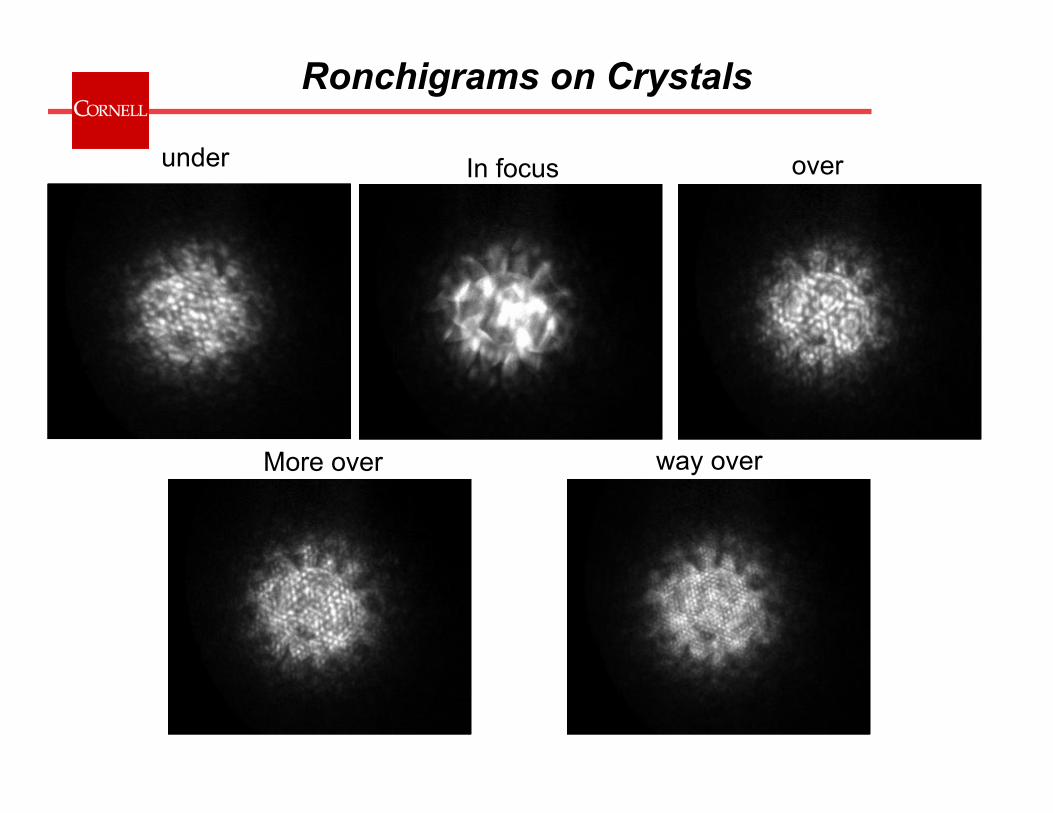
Ronchigrams on Crystals
TiltedIn focus overunder
More over way over
David Muller 2006 42
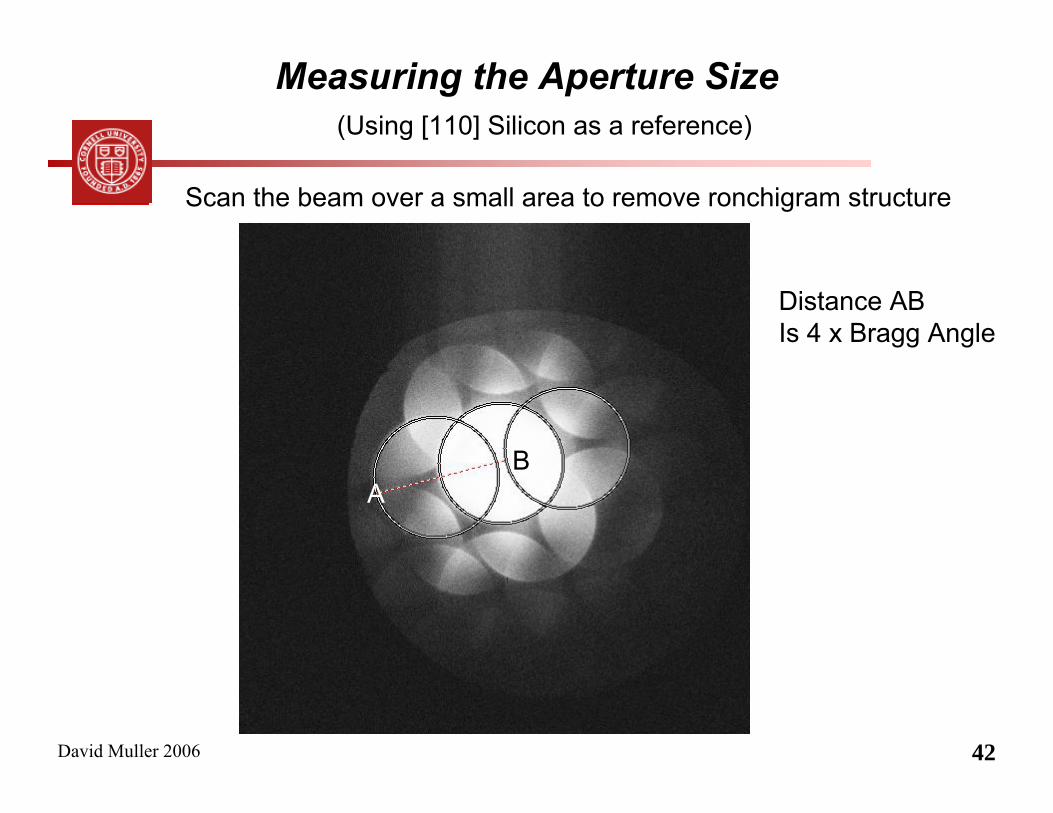
Measuring the Aperture Size(Using [110] Silicon as a reference)
Scan the beam over a small area to remove ronchigram structure
AB
Distance ABIs 4 x Bragg Angle
David Muller 2006 43
Measuring the Aperture Size
David Muller 2006 44
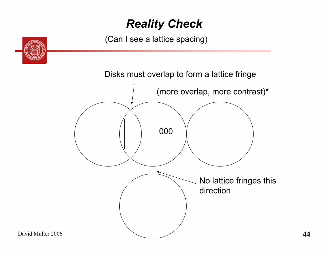
Reality Check(Can I see a lattice spacing)
Disks must overlap to form a lattice fringe
(more overlap, more contrast)*
000
No lattice fringes thisdirection
David Muller 2006 45
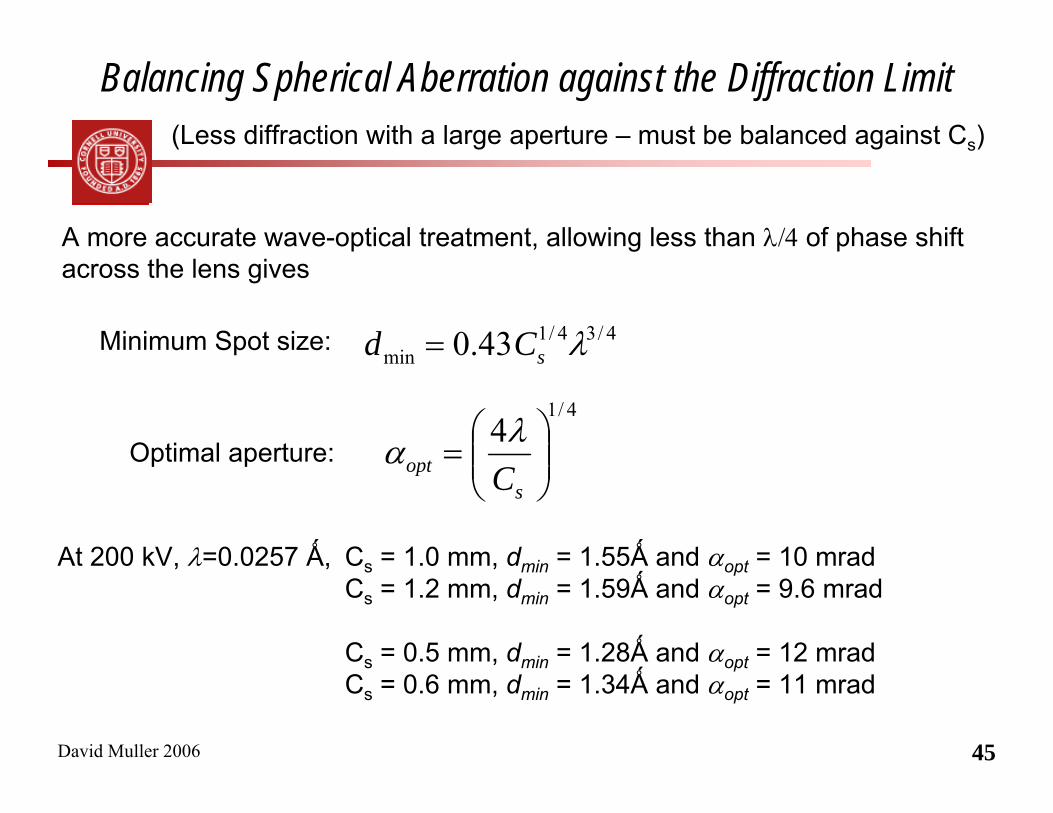
Balancing Spherical Aberration against the Diffraction Limit(Less diffraction with a large aperture – must be balanced against Cs)
4/34/1min 43.0 λsCd =
A more accurate wave-optical treatment, allowing less than λ/4 of phase shift across the lens gives
Minimum Spot size:
4/14
⎟⎟⎠
⎞⎜⎜⎝
⎛=
sopt C
λαOptimal aperture:
At 200 kV, λ=0.0257 Ǻ, Cs = 1.0 mm, dmin = 1.55Ǻ and αopt = 10 mradCs = 1.2 mm, dmin = 1.59Ǻ and αopt = 9.6 mrad
Cs = 0.5 mm, dmin = 1.28Ǻ and αopt = 12 mradCs = 0.6 mm, dmin = 1.34Ǻ and αopt = 11 mrad
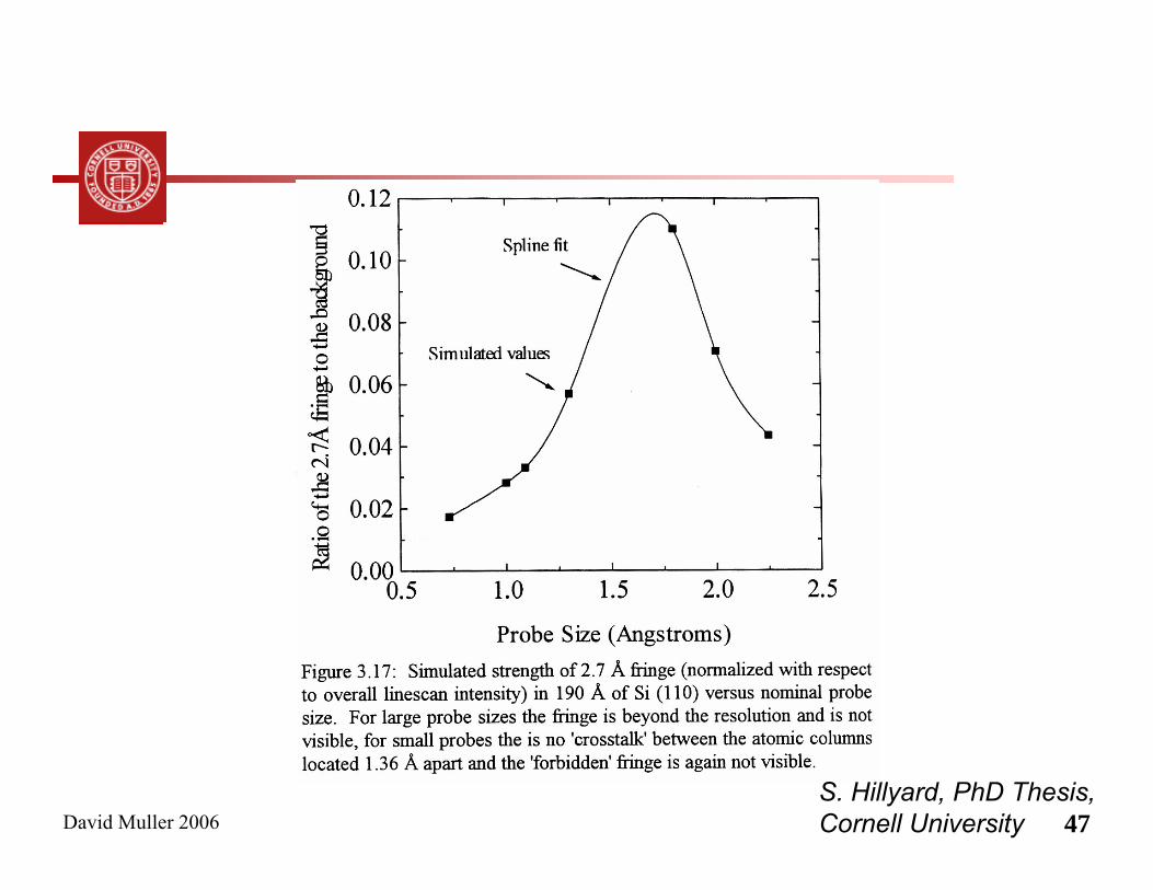
David Muller 2006 46D. Muller, Bell Labs, 1998
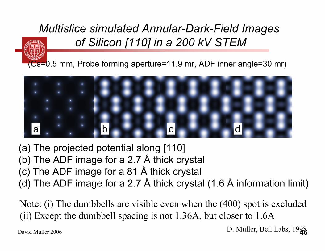
Multislice simulated Annular-Dark-Field Images of Silicon [110] in a 200 kV STEM
c dba
(a) The projected potential along [110](b) The ADF image for a 2.7 Å thick crystal(c) The ADF image for a 81 Å thick crystal(d) The ADF image for a 2.7 Å thick crystal (1.6 Å information limit)
(Cs=0.5 mm, Probe forming aperture=11.9 mr, ADF inner angle=30 mr)
Note: (i) The dumbbells are visible even when the (400) spot is excluded(ii) Except the dumbbell spacing is not 1.36A, but closer to 1.6A
David Muller 2006 47S. Hillyard, PhD Thesis,Cornell University
David Muller 2006 48
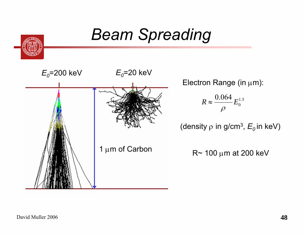
Beam Spreading
E0=200 keV E0=20 keV
1 µm of Carbon
Electron Range (in µm):
5.10
064.0 ERρ
≈
(density ρ in g/cm3, E0 in keV)
R~ 100 µm at 200 keV
David Muller 2006 49
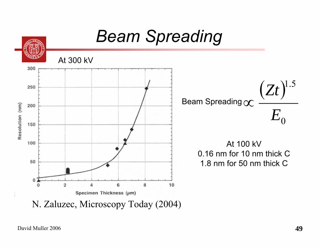
Beam Spreading
Beam Spreading ( )
0
5.1
EZt
∝
At 100 kV0.16 nm for 10 nm thick C1.8 nm for 50 nm thick C
At 300 kV
N. Zaluzec, Microscopy Today (2004)

David Muller 2006 50
0
0.2
0.4
0.6
0.8
1
0 10 20 30 40 50
Bea
m D
iam
eter
(A)
Thickness (A)
Beam Broadening in a-Si at 100kV
Loss of resolution, loss of apparent brightnessIncreased Apparent Source size
•Ignore for probes larger than 0.4Ǻ
How does an amorphous layer on the entrance surface degrade resolution?
•No FIB’ed samples!
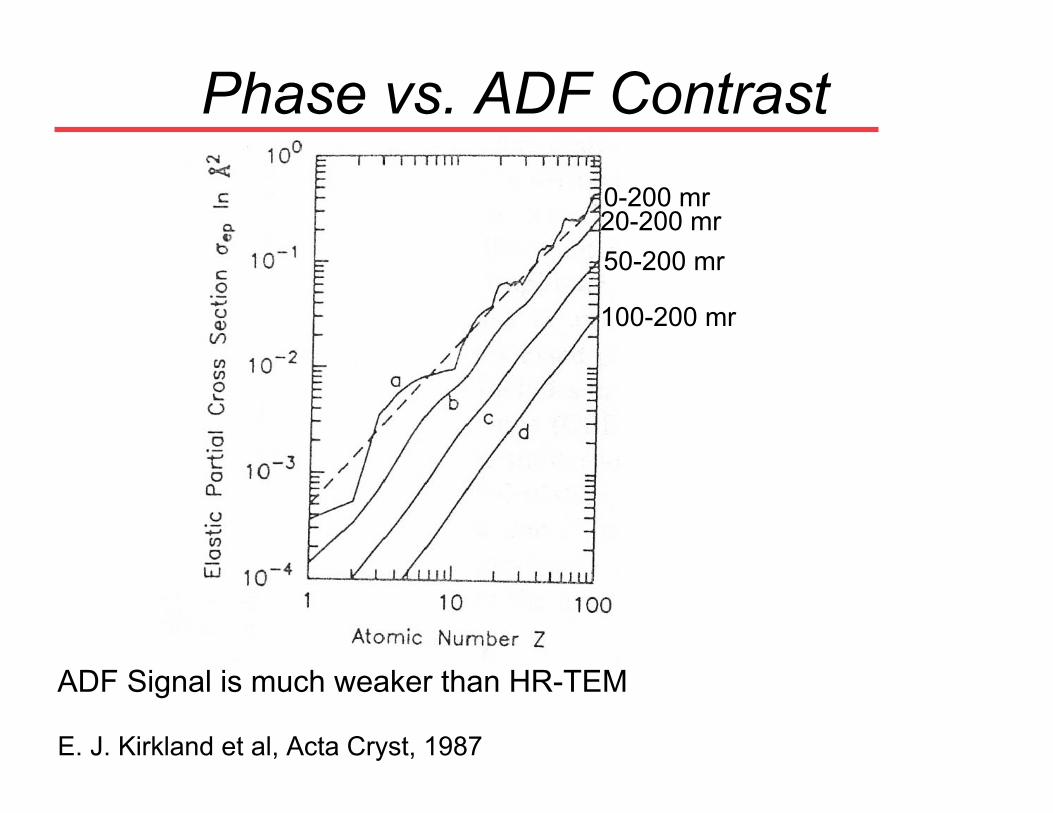
Phase vs. ADF Contrast
David Muller, 2000
ADF Signal is much weaker than HR-TEM
E. J. Kirkland et al, Acta Cryst, 1987
0-200 mr20-200 mr50-200 mr
100-200 mr
David Muller 2006 52
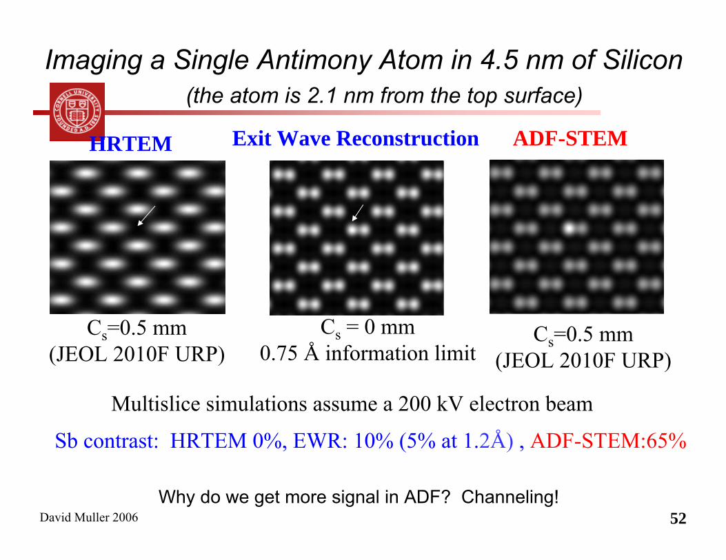
Imaging a Single Antimony Atom in 4.5 nm of Silicon(the atom is 2.1 nm from the top surface)
ADF-STEMExit Wave Reconstruction
Cs = 0 mm0.75 Å information limit
Cs=0.5 mm(JEOL 2010F URP)
Multislice simulations assume a 200 kV electron beam
Sb contrast: HRTEM 0%, EWR: 10% (5% at 1.2Å) , ADF-STEM:65%
HRTEM
Cs=0.5 mm(JEOL 2010F URP)
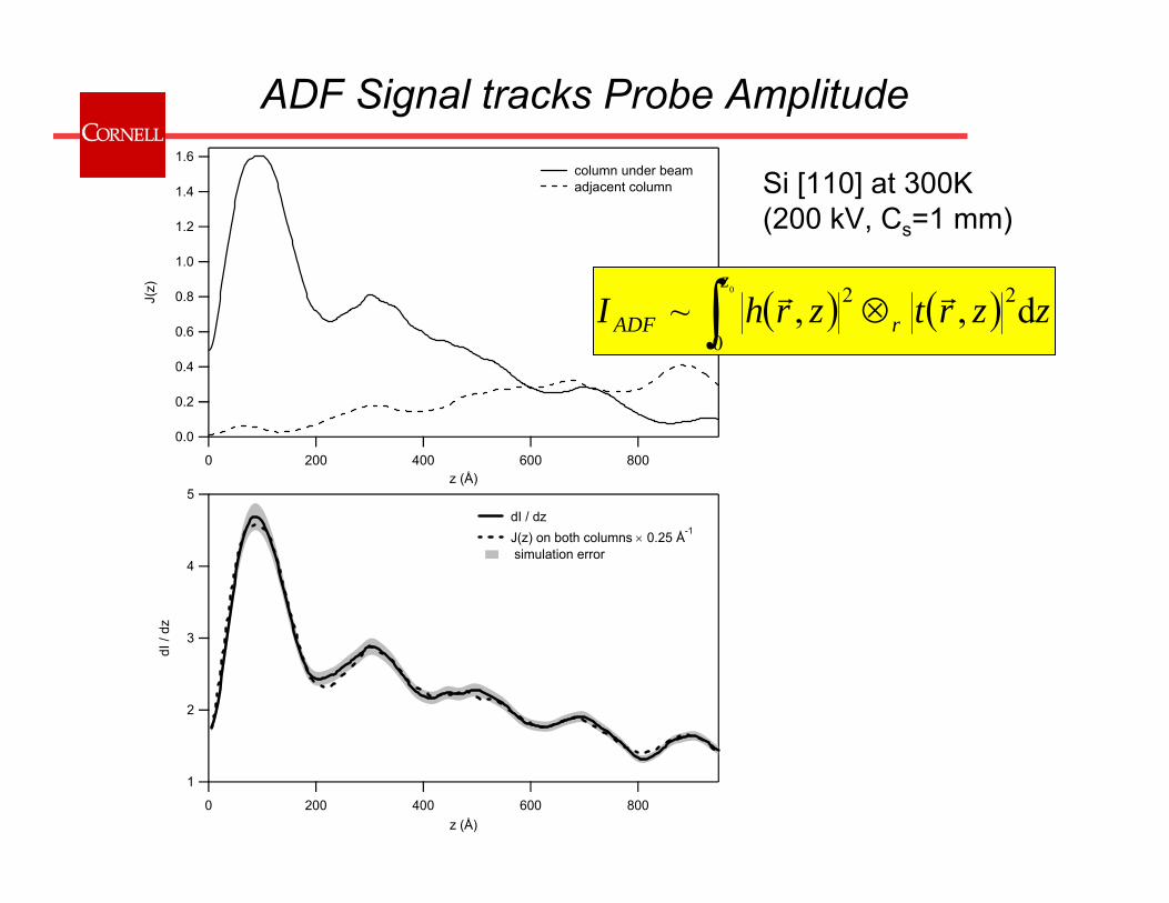
Why do we get more signal in ADF? Channeling!
David Muller 2006 53
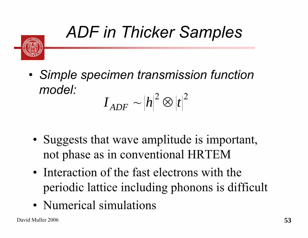
ADF in Thicker Samples
• Simple specimen transmission function model: 22~ thI ADF ⊗
• Suggests that wave amplitude is important, not phase as in conventional HRTEM
• Interaction of the fast electrons with the periodic lattice including phonons is difficult
• Numerical simulations
David Muller 2006 54
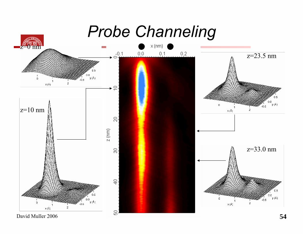
Probe Channelingz=0 nm
z=10 nm
z=33.0 nm
z=23.5 nm
ADF Signal tracks Probe Amplitude1.6
1.4
1.2
1.0
0.8
0.6
0.4
0.2
0.0
J(z)
8006004002000z (Å)
column under beam adjacent column
5
4
3
2
1
dI /
dz
8006004002000z (Å)
dI / dz J(z) on both columns × 0.25 Å-1
simulation error
Si [110] at 300K(200 kV, Cs=1 mm)
( ) ( ) zzrtzrhIz
rADF d,,~0
0
22∫ ⊗ rr
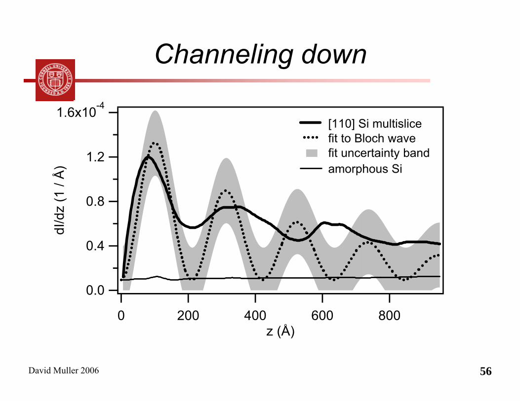
David Muller 2006 56
Channeling down
1.6x10⁻⁴
1.2
0.8
0.4
0.0
dI/d
z (1
/ Å
)
8006004002000z (Å)
[110] Si multislice fit to Bloch wave fit uncertainty band amorphous Si
David Muller 2006 57
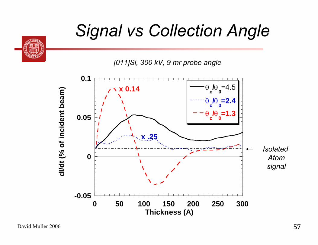
Signal vs Collection Angle
-0.05
0
0.05
0.1
0 50 100 150 200 250 300
θc/θ
0=4.5
θc/θ
0=2.4
θc/θ
0=1.3
dI/d
t (%
of i
ncid
ent b
eam
)
Thickness (A)
x 0.14
x .25
[011]Si, 300 kV, 9 mr probe angle
Isolated Atomsignal
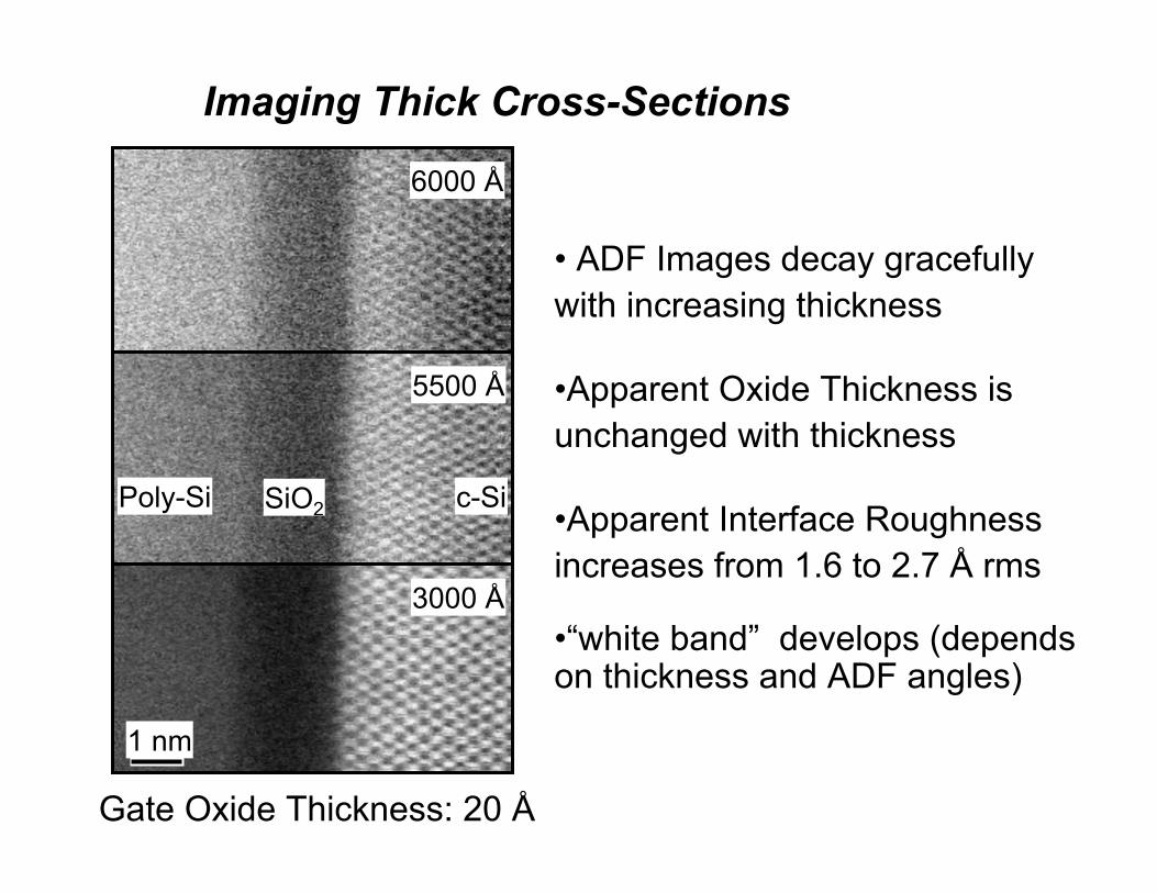
Imaging Thick Cross-Sections
Gate Oxide Thickness: 20 Å
• ADF Images decay gracefully with increasing thickness
•Apparent Oxide Thickness is unchanged with thickness
•Apparent Interface Roughness increases from 1.6 to 2.7 Å rms
•“white band” develops (depends on thickness and ADF angles)
3000 Å
5500 Å
6000 Å
1 nm
Poly-Si c-SiSiO2
David Muller 2006 59
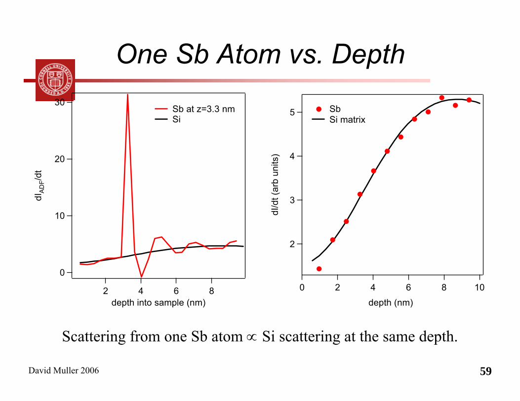
One Sb Atom vs. Depth
Scattering from one Sb atom ∝ Si scattering at the same depth.
30
20
10
0
dIA
DF/
dt
8642depth into sample (nm)
Sb at z=3.3 nm Si
1086420depth (nm)
5
4
3
2
dI/d
t (ar
b un
its)
Sb Si matrix
0.25
0.20
0.15
0.10
0.05
sim
ulat
ed I A
DF
0.25
0.20
0.15
0.10
0.05
sim
ulat
ed I A
DF
3210-1
position (Å)
3210-1
position (Å)
Bi Bi
Bi
(a) no Bi (b) zBi = 20 Å
(c) zBi = 342 Å (d) zBi = 750 Å Wrong columnAppears bright!
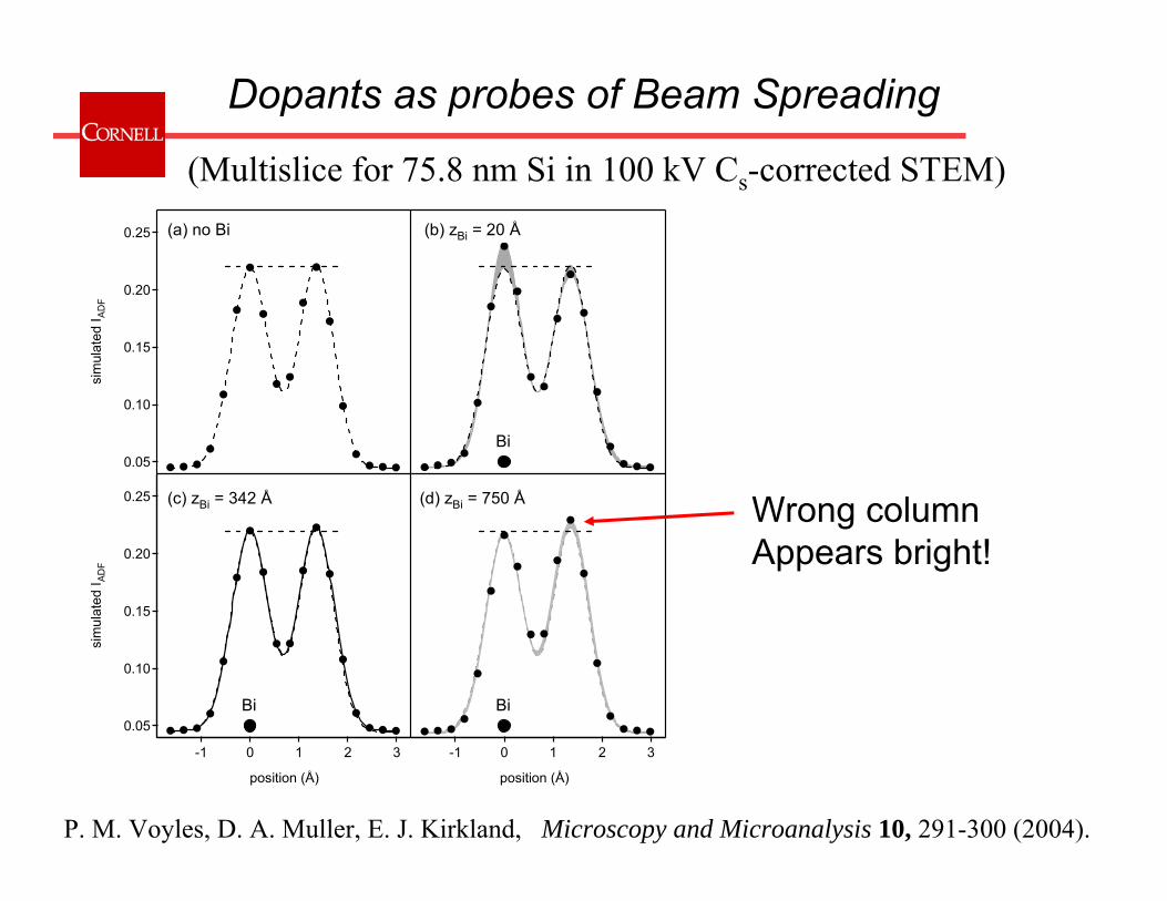
Dopants as probes of Beam Spreading
(Multislice for 75.8 nm Si in 100 kV Cs-corrected STEM)
P. M. Voyles, D. A. Muller, E. J. Kirkland, Microscopy and Microanalysis 10, 291-300 (2004).
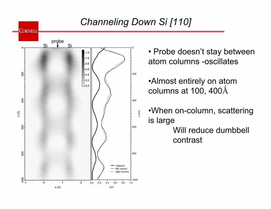
Channeling Down Si [110]
Si Siprobe
1.00.80.60.40.20.0
ψ(z)
1000
800
600
400
200
0
z (n
m)
midpoint left column right column
• Probe doesn’t stay between atom columns -oscillates
•Almost entirely on atom columns at 100, 400Ǻ
•When on-column, scattering is large
Will reduce dumbbell contrast
David Muller 2006 62
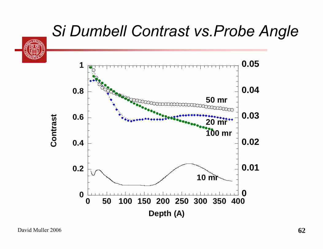
Si Dumbell Contrast vs.Probe Angle
0
0.2
0.4
0.6
0.8
1
0
0.01
0.02
0.03
0.04
0.05
0 50 100 150 200 250 300 350 400
Con
tras
t
Depth (A)
10 mr
100 mr20 mr
50 mr
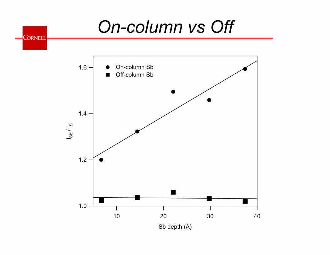
On-column vs Off
1.6
1.4
1.2
1.0
I Sb /
I Si
40302010
Sb depth (Å)
On-column Sb Off-column Sb
David Muller 2006 64
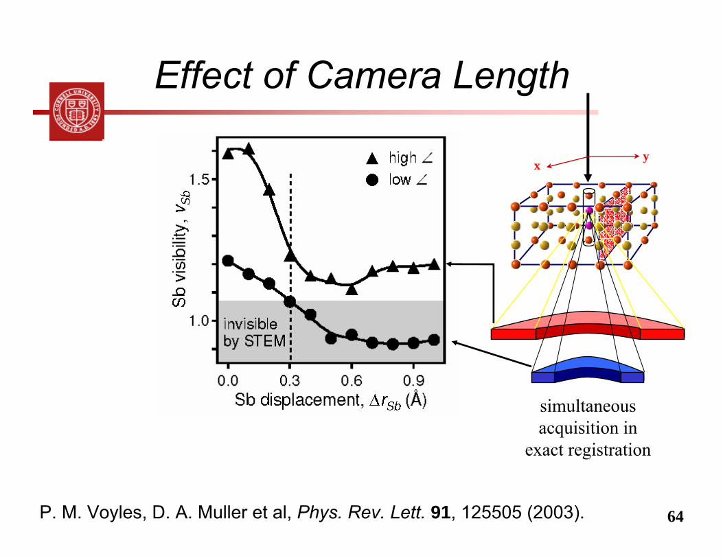
Effect of Camera Length
yx
simultaneous acquisition in
exact registration
P. M. Voyles, D. A. Muller et al, Phys. Rev. Lett. 91, 125505 (2003).
David Muller 2006 65
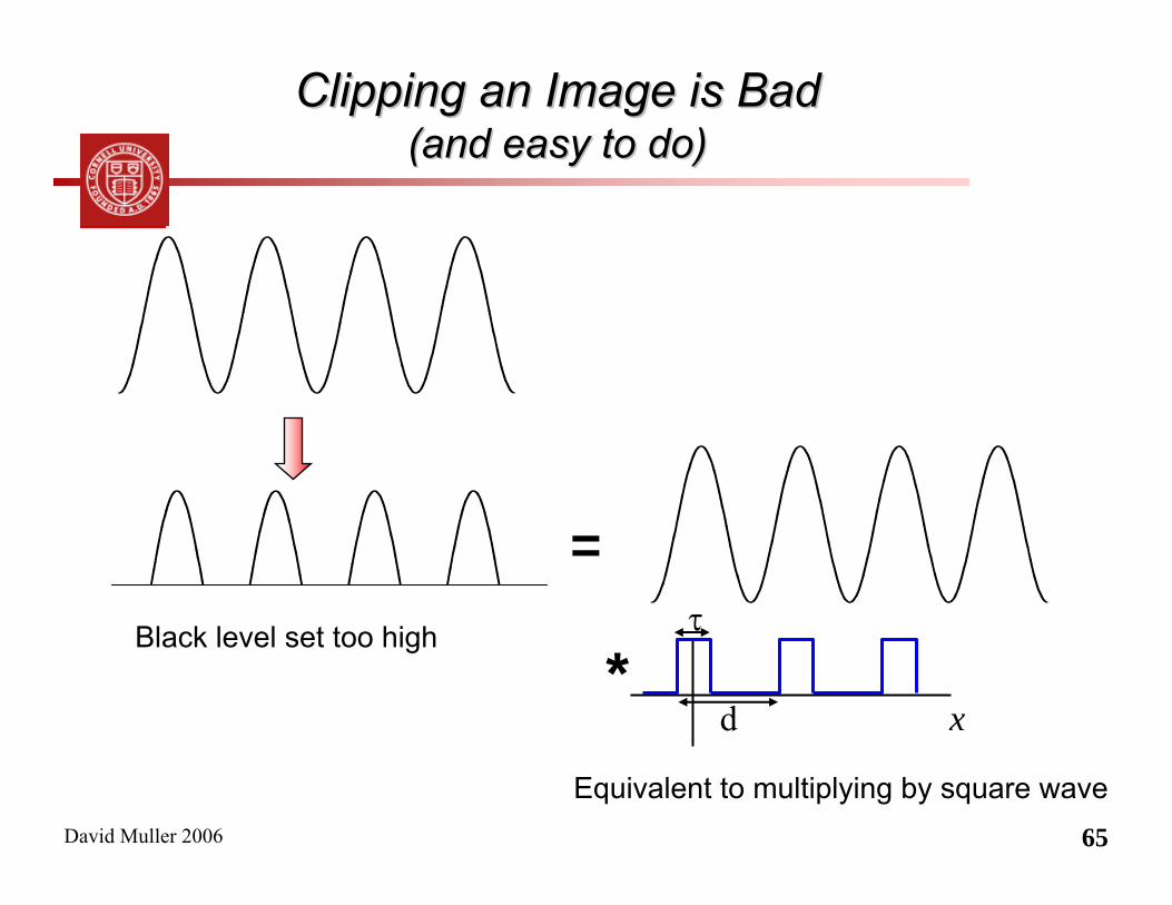
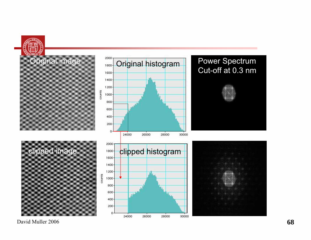
Clipping an Image is BadClipping an Image is Bad(and easy to do)(and easy to do)
x
τ
d
=Black level set too high
*
Equivalent to multiplying by square wave
David Muller 2006 66
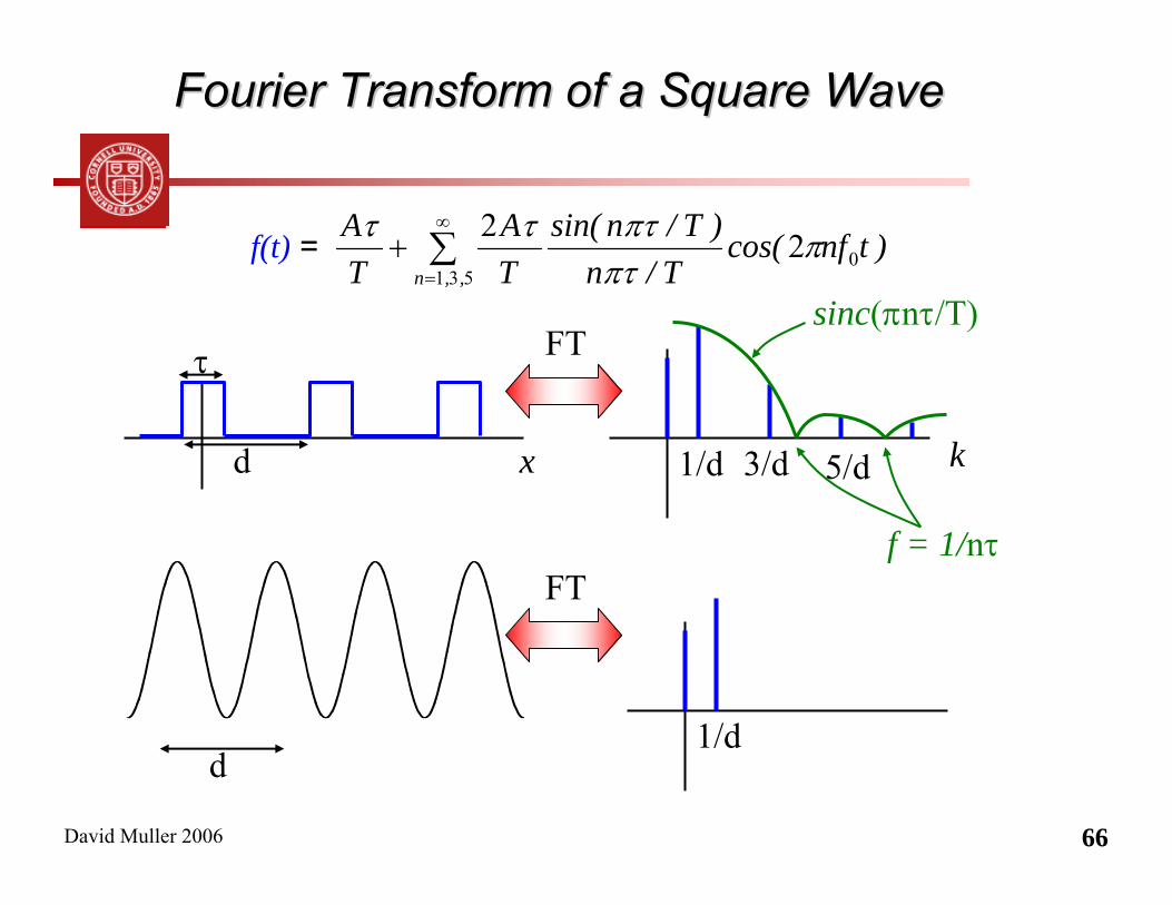
Fourier Transform of a Square WaveFourier Transform of a Square Wave
x
τ
d k1/d 5/d3/d
sinc(πnτ/T)
f = 1/nτ
FT
f(t) = )tnfcos(T/n
)T/nsin(TA
TA
,,n0
53122 π
πτπτττ
∑∞
=+
FT
d1/d
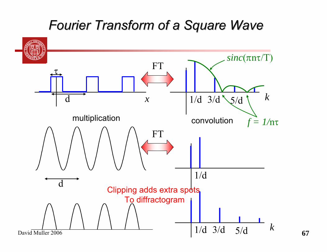
David Muller 2006 67
Fourier Transform of a Square WaveFourier Transform of a Square Wave
x
τ
d k1/d 5/d3/d
sinc(πnτ/T)
f = 1/nτ
FT
FT
d1/d
multiplication convolution
Clipping adds extra spots To diffractogram
k1/d 5/d3/d
David Muller 2006 68
Original image
clipped image
Original histogram Power SpectrumCut-off at 0.3 nm
clipped histogram
David Muller 2006 69
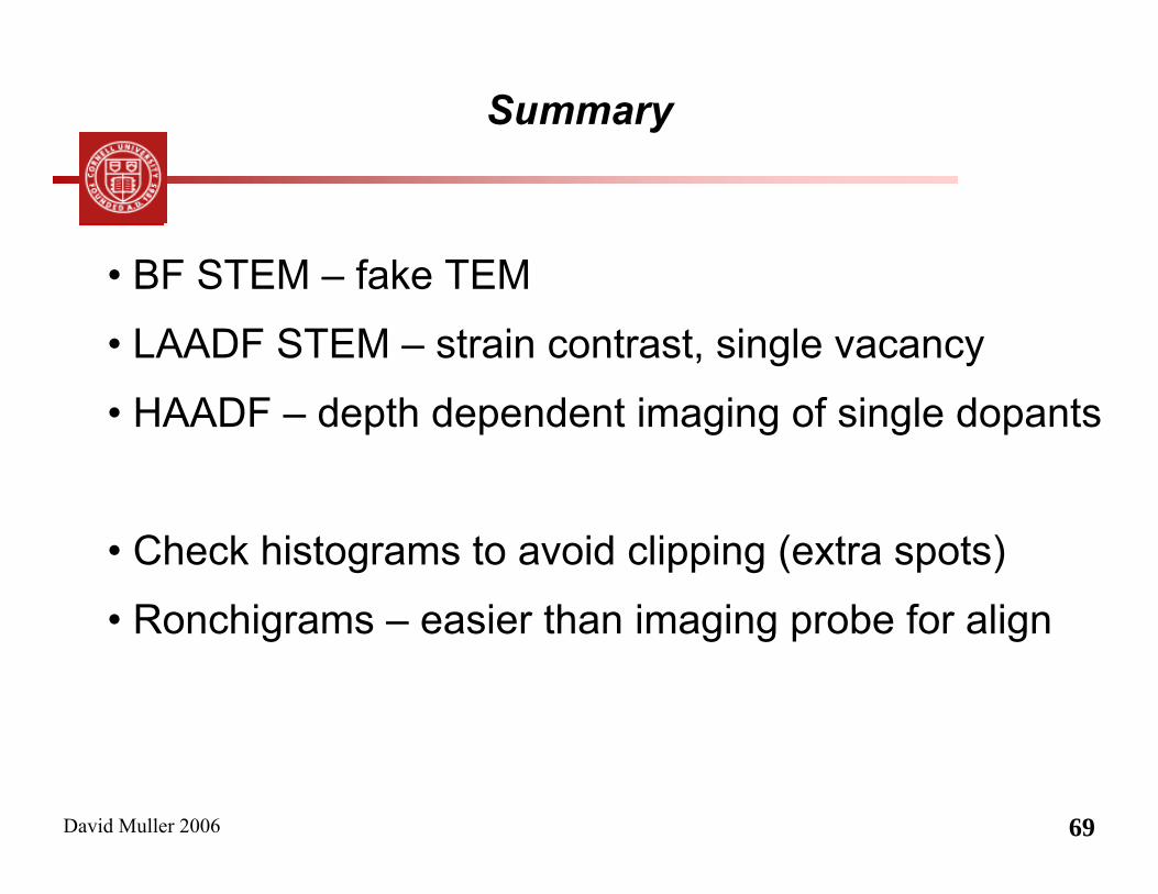
Summary
• BF STEM – fake TEM
• LAADF STEM – strain contrast, single vacancy
• HAADF – depth dependent imaging of single dopants
• Check histograms to avoid clipping (extra spots)
• Ronchigrams – easier than imaging probe for align
David Muller 2006 70
Comparison of Brightness MeasurementsFor Cold and Thermal Field Emitters
David MullerApplied and Engineering Physics
Cornell University
• Few good measurements of Brightness.
• Need to measure or extract the source size (easy to overestimate)
• No reliable studies of Brightness vs. Field, Temperature or monochromation
Current State of the Art:
David Muller 2006 71
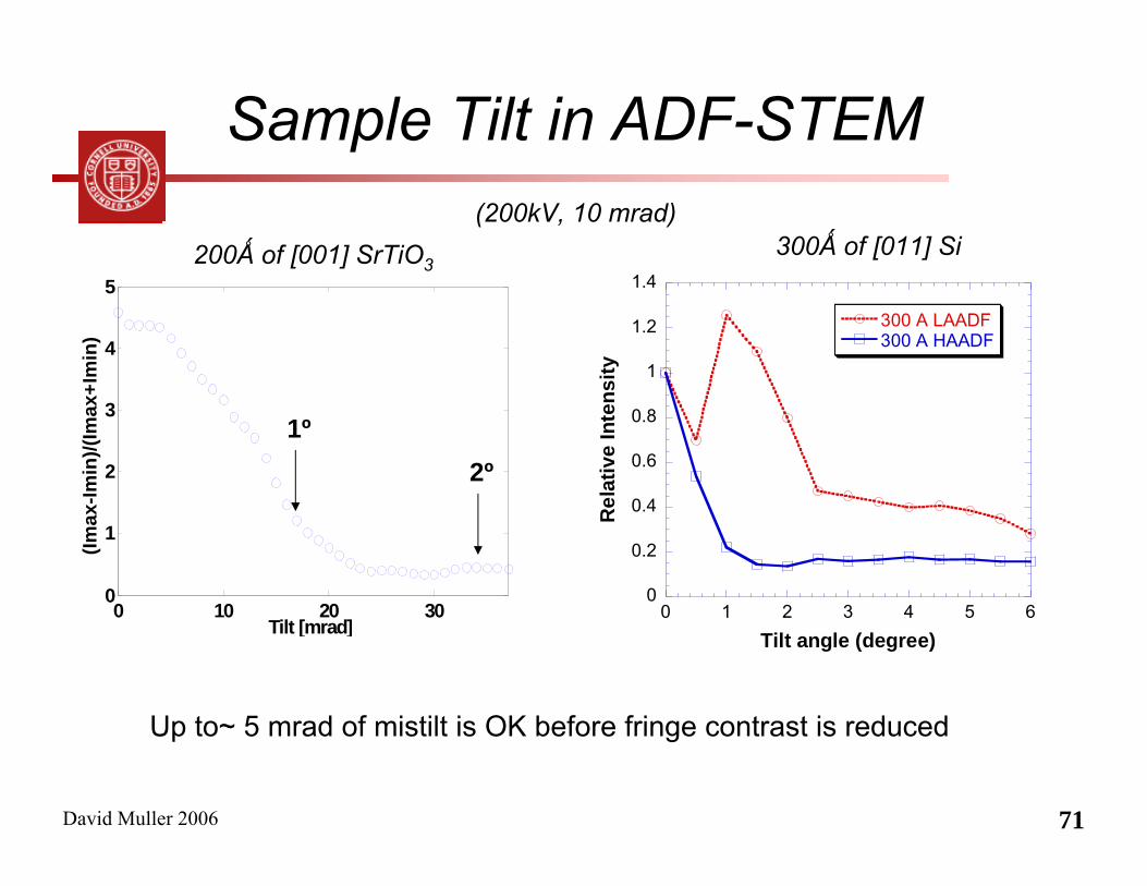
Sample Tilt in ADF-STEM
0 10 20 300
1
2
3
4
5
Tilt [mrad]
(Imax
-Imin
)/(Im
ax+I
min
)
0
0.2
0.4
0.6
0.8
1
1.2
1.4
0 1 2 3 4 5 6
300 A LAADF300 A HAADF
Rel
ativ
e In
tens
ityTilt angle (degree)
300Ǻ of [011] Si200Ǻ of [001] SrTiO3
1º2º
Up to~ 5 mrad of mistilt is OK before fringe contrast is reduced
(200kV, 10 mrad)


![Idris 2006 Cprs District I Id2digest Summer06[1] ادريس جاسم العبودي](https://img.pdfslide.us/doc/110x75/54c25b314a7959db1f8b45ed/idris-2006-cprs-district-i-id2digest-summer061-.jpg)