Embed Size (px)
Citation preview

Control element for high voltage power supplies
Features • 5VControl • 8kVBiasVoltage • CurrentTransferRatio≥0.6% • LowLeakageCurrent • 12kVIsolationVoltage • RadiationTolerantto105 rad(Si) • Upto100V/µsslewrate(10pFload) • Smallfootprint • BackwardcompatibletoHV601B
Applications • PhotoelectronMicroscopy • ElectrostaticDeflectionPlates • Spaceinstrumentation
• Electrostaticanalyzers • Highvoltagepowersupplies • Regulatedcurrentsource • HighVoltagerelay • HighVoltagebipolaramplifier
General DescriptionThe HV801 is a high voltage optocoupler developed as a control element for High Voltage Power Supplies. It consists of a multiple junction high voltage diode, optically coupled to three infrared emitting LEDs in series. The photocurrent in the output diodes is proportional to the light produced by the LEDs. The ratio of the output photocurrent to the LED input current is the current transfer ratio (CTR) of the device. The HV801 provides high breakdown voltage, low leakage current, and a fast slew rate, making it ideal for use in a wide range of high voltage power supply applications. It provides linear control of volt-ages up to 8 kV and is current controlled from a convenient 5 V source. It is supplied in a small size, high dielectric strength, space rated epoxy package.
Amptek Inc. 14 DeAngelo Drive, Bedford, MA 01730-2204 USATel: +1 781 275-2242 Fax: +1 781 275-3470 E-mail: [email protected] http://www.amptek.com
8 kV
≥ 0.6%
4
1 2
3
HV801
Z-LOAD
lout
lout
lin
lin
Typical Application
HV801
(Rev D5)
Showninactualsize
Page1

1. NondestructiveBondPull(100%) MIL-STD-883,Method2023
2. VisualInspection MIL-STD-883,Method2017
3. Encapsulation Lowoutgassingepoxypackage
4. Marking SerialNumber,DateCode,ID
5. ElectricalTest At+25°C
6. TemperatureCycling MIL-STD-883,Method1010,(modified)T=-35°Cto100°C,15cycles,4min.eachextreme,3min.maximumtransfertime
7. ElectricalTest At+25°C
8. Radiographic MIL-STD-883,Method2012
9. Burn-in MIL-STD-883,Method1015,320hrs@90°C
10. FinalElectricalTest At+80°C,+25°Cand-35°C
QC Periodic Tests
11. LifeTestonsampledevices 1000hours(total)Burn-Inat+90°CwithadditionalinterimandFinalElectricalTestsat+80°C,+25°Cand-35°C
12. TemperatureCycling 100cyclesasinstepnumbersixabove
Input CharacteristicsThe input (Pins 1 and 2) behaves as a diode with a nominal threshold voltage of 3.1 volts. Output current (Pins 3 and 4) is controlled by varying the input current in the range of 0 to 100 mA. Input current should be limited such that the total power dissipated in the device is less than 0.5 watt at ambient conditions. Consideration should be given to the input circuit such that the input reverse bias does not exceed 5 volts.
Output CharacteristicsIn the normal mode of operation, the output cathode (Pin 4) is more positive than the output anode (Pin 3). In this mode the output current is proportional to the input current. The current transfer ratio is guaranteed to be >0.6% at zero bias and 20 mA input current, at 25 °C. The CTR generally increases with bias voltage and input current, to a typical maximum of 2% to 4%. Output slew rate is typically 100 V/μs into a 10 pF load. If Pin 3 is made more positive than Pin 4, the output will act like a forward biased diode with a nominal threshold voltage of 3.5 volts. Amptek offers an HV801RH, or rad-hard, option. The light output of LEDs is well known to decrease with displacement damage, i.e., due to penetrating protons in space. The RH option uses an alternate LED, which has a lower initial light output but which decreases more slowly with proton fluence. The HV801RH CTR is >0.2%. The two parts are otherwise identical.
SPECIFICATIONS
Absolute Maximum Ratings (T=21°C)
InputCurrent:ContinuousPulse(10μs,100Hz)
100mA1A
InputReverseVoltage 5V
JunctionTemperature 100°C
OutputBiasVoltage 8kV
OperatingTemperature(SeeThermalConsiderationsnextpage) -35°Cto+100°C
StorageTemperature -35°Cto+100°C
Electrical Characteristics (T=21°C)
Parameter Symbol Conditions Min. Typ. Max. Units
ReverseBreakdownVoltage VBR ID=1μA >10.0 kV
CurrentTransferRatio
HV801
HV801
HV801RH
HV801RH
CTR
Iin=20mA,Vbias=0V
Iin=20mA,Vbias=6kV
Iin=20mA,Vbias=0V
Iin=20mA,Vbias=6kV
0.6
0.2
1.6
0.8
%
%
%
%
DarkCurrent ID VB=8kV 10.0 250 nA
OutputCapacitance CO VJ=0V 8.0 pF
InputVoltage Vin IIN=20mA 4.0 V
IsolationCapacitance CISO0.6 pF
IsolationVoltage VISO 12.0 kV
Stress above those listed under Absolute Maximum Ratings may cause permanent damage to the device. Exposure to absolute maximum condi-tions for extended periods may affect device reliability.
Page2
0.000
0.005
0.010
0.015
0.020
0.025
1
10
12
34
56
7
Typical HV80125oC
0.000 0.005 0.010 0.015 0.020 0.025
Current Transfer Ratio (CTR) vs Input Current and Bias
CTR
Bias (kV) LED C
urrent (
mA)
HV801 and HV801RH OPTION A+ SCREENING1. NondestructiveBondPull(100%) MIL-STD-883,Method2023
2. VisualInspection MIL-STD-883,Method2017
3. Encapsulation Lowoutgassingepoxypackage
4. Marking SerialNumber,DateCode,ID
5. ElectricalTest At+25°C
6. TemperatureCycling MIL-STD-883,Method1010,(modified)T=-35°Cto100°C,15cycles,4min.eachextreme,3min.maximumtransfertime
7. ElectricalTest At+25°C
8. Radiographic MIL-STD-883,Method2012
9. Burn-in MIL-STD-883,Method1015,320hrs@90°C
10. FinalElectricalTest At+80°C,+25°Cand-35°C
QC Periodic Tests
11. LifeTestonsampledevices 1000hours(total)Burn-Inat+90°CwithadditionalinterimandFinalElectricalTestsat+80°C,+25°Cand-35°C
12. TemperatureCycling 100cyclesasinstepnumbersixabove
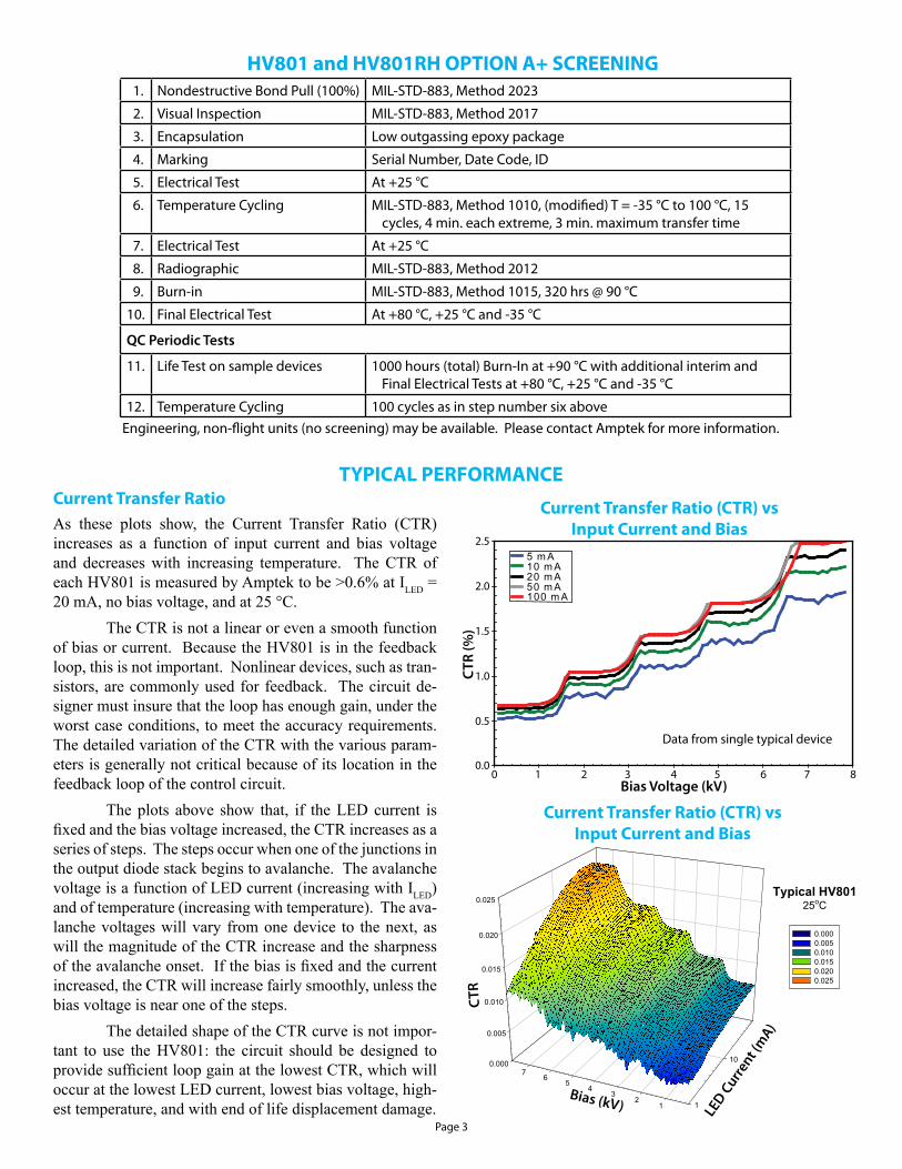
TYPICAL PERFORMANCECurrent Transfer RatioAs these plots show, the Current Transfer Ratio (CTR) increases as a function of input current and bias voltage and decreases with increasing temperature. The CTR of each HV801 is measured by Amptek to be >0.6% at ILED = 20 mA, no bias voltage, and at 25 °C. The CTR is not a linear or even a smooth function of bias or current. Because the HV801 is in the feedback loop, this is not important. Nonlinear devices, such as tran-sistors, are commonly used for feedback. The circuit de-signer must insure that the loop has enough gain, under the worst case conditions, to meet the accuracy requirements. The detailed variation of the CTR with the various param-eters is generally not critical because of its location in the feedback loop of the control circuit. The plots above show that, if the LED current is fixed and the bias voltage increased, the CTR increases as a series of steps. The steps occur when one of the junctions in the output diode stack begins to avalanche. The avalanche voltage is a function of LED current (increasing with ILED) and of temperature (increasing with temperature). The ava-lanche voltages will vary from one device to the next, as will the magnitude of the CTR increase and the sharpness of the avalanche onset. If the bias is fixed and the current increased, the CTR will increase fairly smoothly, unless the bias voltage is near one of the steps. The detailed shape of the CTR curve is not impor-tant to use the HV801: the circuit should be designed to provide sufficient loop gain at the lowest CTR, which will occur at the lowest LED current, lowest bias voltage, high-est temperature, and with end of life displacement damage.
Current Transfer Ratio (CTR) vs Input Current and Bias
5 m A10 m A20 m A50 m A100 m A
CTR
(%)
2.5
2.0
1.5
1.0
0.5
0.0
012345678Bias Voltage (kV)
Datafromsingletypicaldevice
Page3
Engineering,non-flightunits(noscreening)maybeavailable.PleasecontactAmptekformoreinformation.

TYPICAL PERFORMANCE (con’t)
Plotshowingthediodecurve,theforwardvoltageacrosstheLEDstackinatypicalHV801,asafunctionofcurrent,attemperaturesfrom-50to+90°C.
LED Forward Voltage
Plot showing variation in forward voltage versus cur-rent, for fourHV801s fromdifferent lots,at -50°Candat+70°C.
HV801LED Forward Voltage
SN1209
0
20
40
60
80
100
120
3.0 3.5 4.0 4.5 5.0 5.5
Forward Voltage (V)
Cur
rent
(mA
)
-50 C-30 C-10 C 10 C 30 C 50 C 70 C 90 C
HV801LED Forward Voltage
0
20
40
60
80
100
120
3.0 3.5 4.0 4.5 5.0 5.5
Forward Voltage (V)
Cur
rent
(mA
)
-50 oC+70 oC
Current Transfer Ratio (CTR) vs Temperature1.0
0.9
0.8
0.7
0.6
0.5
0.4
0.3
0.2
0.1
0-50 -25 0 25 50 75 100
CTR
(%)
VB = 0
Temperature (°C)
Dark Current vs Bias Voltage
I d (nA
)
1000
100
10
1 0 2 4 6 8 10 12VB (kV)20 25 30 35 40 45 50 55 60
80
70
60
50
40
30
20
10
0
Id (n
A)
Dark Current vs Temperature
Temperature (°C)
Drive Voltage vs Temperature
Temperature (°C)
Volt
age
(V)
4.5
4.4
4.3
4.2
4.1
4.0
3.9
3.8
3.7
3.6
3.5-60 -40 -20 0 20 40 60 80 100
Iin = 20 mA
Average
TypicalRange
Dark CurrentTheHV801isratedforamaximumof8kVbias.Themaximumdarkcurrentat8kVis250nAbuttheaverageisunder10nAat25°C.Thedarkcurrentapproximatelydoublesforevery10°Cincreaseintemperature.EachHV801istestedat10kV,beyonditsratedvoltage,toverifythatbreakdownvoltageis>10kV.Asseenintheplot,thedarkcurrentisnearlyindepen-dentofbiasat8kVandbelow,butincreasestoatypicallyvalueof70nAat10kV.
Page4

HV801LED Forward Voltage
0
20
40
60
80
100
120
3.0 3.5 4.0 4.5 5.0 5.5
Forward Voltage (V)
Cur
rent
(mA
)
-50 oC+70 oC
-60 -40 -20 0 20 40 60 80 100
Dark Current Test CircuitCTR Test Circuit at
Unbiased Conditions
HV801
1 2
34
A
AMMETER
HV DIODE STACK
LED ARRAY
CURRENTSOURCE
Typical photocurrent lout = 120 µA
Typicallin = 20 mA
CTR Test Circuit at Biased Conditions
CURRENTSOURCETypical
lin = 20 mA
1 2
34 A
AMMETER
HV DIODE STACK
LED ARRAYHV
HV801
10 M
CURRENTSOURCE
Typical photocurrentlout = 120 µA
Typicallin = 20 mA
1 2
34 A
AMMETER
HV DIODE STACK
LED ARRAYHV
HV801
10 M
TYPICAL PERFORMANCE (con’t)
Thermal Resistance
θj-l θj-l
HV diodejunction
LED diodejunction
θj-lθj-l
θj-c
θj-c
θj-l is the thermal resistance from the junction to a single lead.
Note: If both leads are connected to the PCB, the total thermal resistance is ½ θj-l
θj-c is the thermal resistance from the junction to the case
θj-l °C/W θj-c °C/W
HV diode 31 38LED 74 44
Forassemblyandsolderingreferto: IPC-A-610 IPC-HDBK-001
Thermal ConsiderationsThe maximum power dissipation and derating considerations must be specified so that the TJ, the junctions of the diodes, do not exceed 100 °C.
Application ExampleConsider an example where the four leads provide the thermal path to the PCB, assumed to be at ambient. This gives θJA = 15 °C/W for the HV stack and 37 °C/W for the LEDs. Assume Iin = 10 mA, with VF = 4 V, Vbias = 5 kV, and CTR = 2%, so Iout = 200 µA. The power dissipations will be 40 mW in the LEDs and 1 W in the HV diode stack. This yields a ΔT of 15 °C for the HV diode stack and 1.5 °C for the LEDs. This unit can be operated at an ambient temperature of 82 °C (printed circuit board temperature).Note that the CTR is a function of bias voltage, current, temperature, and exhibits manufacturing variability. The user must examine all these parameters closely if operation near the maximum junction temperature is anticipated.This calculation, though simple, does not represent the typical usage of an HV801. An HV801 is most often used to control rapidly a stepped voltage, i.e., biasing the deflection electrodes in an electrostatic analyzer. The current only flows for a brief period at the beginning of each step, i.e., there is a very low duty cycle. The total power dissipation is reduced greatly. Typical applications exhibit tens of mW of total power.
Page5

Radiation DamageTotal Ionizing Dose: 100 krad (Si). The HV801 and HV801RH were tested to 100 krads (Si), using 60Co gamma-rays. The CTR for the HV801 de-
creased by 7.6%. The CTR for the HV801RH was unchanged. No measurable change was found for the other parameters.
Displacement Damage As is well known, the LEDs are generally susceptible to displacement damage. The plot below shows typical
results which are expected for the HV801 and the HV801RH when tested with 50 MeV protons. These results here are typical of the both the packaged devices and the LEDs used in the two parts. The HV diode stack is not susceptible to displacement damage at these levels.
0.0E+00 2.0E+10 4.0E+10 6.0E+10 8.0E+10 1.0E+11
8.0E-03
0.0E-03
2.0E-03
4.0E-03
6.0E-03
HV801HV801RH
CTR
Fluence (50 MeV p / cm )+ 2
TYPICAL PERFORMANCE (con’t)
PIN1:Input,positivePIN2:Input,negativePIN3:Output,negativePIN4:Output,positive
4
3
21
HV+
HV
+_
_
PACKAGE DIMENSIONS0.400
(10.16)
0.200 (5.08)
HV StackCathode4 3
1 2
HV StackAnode
LEDAnode
0.400 (10.16)
0.150 (3.81)
0.100 (2.54)
0.100 (2.54)
0.300 (7.62)
0.100 (2.54)
LEDCathode
0.030 (0.76)Diameter
0.025 (0.63)
0.020 (0.50)
Beryllium CopperPrimed with solder
Copper withNi / Au plating
Ininches(millimeters)
PACKAGE DIAGRAM
Page6
Weight:1.53grams

Simplified Schematic of a Low Power High Voltage Circuit Using the HV801
UUUUUUUUUUUU
ClockReset
Sweep
Reference
To ElectronAnode (+2500 V)
+28 VDC
VoltageMultiplier
Oscillator
Return(28 VDC)
Electron MCP
Ion MCP
+2400 V
+400 V
+2700VDC
-3600VDC
-2100 V
-100 V
+2700 VDC
+2500 V
+2.5 V
+2700 VDC
-3600 VDC
-3400 V
-3.4 V
Ion OuterSphere
Electron InnerSphere
Ion InnerSphere
Electron OuterSphere
HV801
HV801
APPLICATIONS for HV801
Simplified Bipolar Power Supply
2
3
4
1+_
+_
+
_
4
1
2
3
12
3
HV801
HV8017 kV
7 kV
Reference
LOAD
Page7
Burn-in Circuit
20 mA
5 kV
R169.8
U1AMPTEK HV801
Q1R1100 M
ON: 4.17 mS
50 mS
1 4
2
3
1
2
3