Embed Size (px)
Citation preview
RADIOENGINEERING, VOL. 24, NO. 3, SEPTEMBER 2015 661
DOI: 10.13164/re.2015.0661 FEATURE ARTICLE
Applications of Graphene at Microwave Frequencies
Maurizio BOZZI1,2, Luca PIERANTONI2,3, Stefano BELLUCCI2 1 Dept. of Electrical, Computer, and Biomedical Engineering, University of Pavia, Via Ferrata, 5, Pavia, 27100, Italy
2 INFN-Laboratori Nazionali di Frascati, Via E. Fermi 40, Frascati, 00044, Italy 3 Università Politecnica delle Marche, Ancona, 60131, Italy
[email protected], [email protected], [email protected]
Abstract. In view to the epochal scenarios that nanotech-nology discloses, nano-electronics has the potential to introduce a paradigm shift in electronic systems design similar to that of the transition from vacuum tubes to semi-conductor devices. Since low dimensional (1D and 2D) nano-structured materials exhibit unprecedented electro-mechanical properties in a wide frequency range, includ-ing radio-frequencies (RF), microwave nano-electronics provides an enormous and yet widely undiscovered opportunity for the engineering community. Carbon nano-electronics is one of the main research routes of RF/micro-wave nano-electronics. In particular, graphene has shown proven results as an emblematic protagonist, and a real solution for a wide variety of microwave electronic devices and circuits. This paper introduces graphene properties in the microwave range, and presents a paradigm of novel graphene-based devices and applications in the micro-wave/RF frequency range.
Keywords Nanotechnology, carbon nano-electronics, graphene, graphene nano-ribbons, plasmonics, ballistic electronics, graphene transistor, graphene antenna, graphene attenuator, graphene composites
1. Introduction Nano-technology can be defined as that part of mod-
ern technology enabling the practical exploitation of nano-scale science and technology from a multidisciplinary per-spective, including electronics [1]. Nano-technology and nano-electronics not only yield miniaturization of devices and enhancement of integration density but also feature unusual physical, chemical, biological properties, thus i) leading to novel theoretical concepts, ii) requiring multi-scale/multiphysics modeling and simulation tools, aimed at including quantum transport, electromagnetics, thermal, mechanical, opto-mechanical phenomena, iii) involve novel technology and metrology foundations [2], [3].
The goal of dealing with the key-development i)-iii), is bridging the gap between the nano-science and a new
Fig. 1. Radio-Frequency nano-electronics: bridging from
theoretical foundations to a new generation of devices, circuits and systems.
generation of extremely integrated devices, circuits and systems, as depicted in Fig. 1.
Driven by technology and market requirements, semi-conductor electronics has already found its way into the nanoscale dimensions. In fact, the continuing technological progress in silicon complementary metal–oxide–semicon-ductor (CMOS) technology, following Moore’s law, still holds potentials for advances.
However, novel devices based on a combination of new materials and advanced technologies already existing will be required to go beyond the scaling limits of Silicon. A multitude of exciting research projects based on novel materials and nano-science concepts have been developed to pave the way for a new generation of nano-electronic devices and systems, yielding not only higher integration densities but also substantially improved electro-thermal-mechanical properties.
It is remarkable to note that nano-scale/structured materials and devices, and, in particular, low-dimensional 1D and 2D materials, namely carbon nanotubes (CNT), graphene, 2D-materials “beyond graphene”, exhibit their most thermo-electro-mechanical properties over a broad range of applications and operating frequencies, covering a wide energy/frequency spectrum, thus including RF/microwave [4].
Due to its particular band structure, graphene exhibits superior performances, as high carriers mobility, thermal conductivity, unprecedented mechanical properties, tun-ability, ambipolarity. In the ballistic regime, electrons and holes can be described by mass-less fermions with a linear energy dispersion relation [5–9].
662 M. BOZZI, L. PIERANTONI, S. BELLUCCI, APPLICATIONS OF GRAPHENE AT MICROWAVE FREQUENCIES
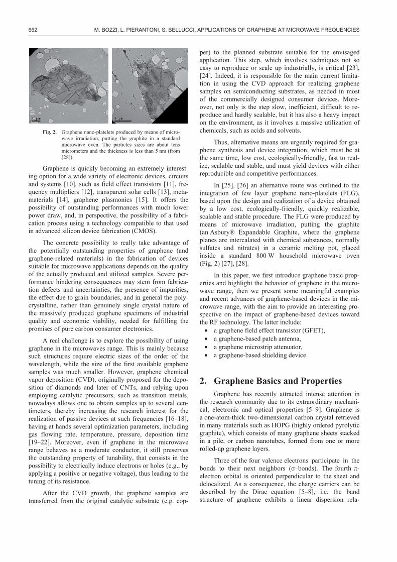
Fig. 2. Graphene nano-platelets produced by means of micro-wave irradiation, putting the graphite in a standard microwave oven. The particles sizes are about tens micrometers and the thickness is less than 5 nm (from [28]).
Graphene is quickly becoming an extremely interest-ing option for a wide variety of electronic devices, circuits and systems [10], such as field effect transistors [11], fre-quency multipliers [12], transparent solar cells [13], meta-materials [14], graphene plasmonics [15]. It offers the possibility of outstanding performances with much lower power draw, and, in perspective, the possibility of a fabri-cation process using a technology compatible to that used in advanced silicon device fabrication (CMOS).
The concrete possibility to really take advantage of the potentially outstanding properties of graphene (and graphene-related materials) in the fabrication of devices suitable for microwave applications depends on the quality of the actually produced and utilized samples. Severe per-formance hindering consequences may stem from fabrica-tion defects and uncertainties, the presence of impurities, the effect due to grain boundaries, and in general the poly-crystalline, rather than genuinely single crystal nature of the massively produced graphene specimens of industrial quality and economic viability, needed for fulfilling the promises of pure carbon consumer electronics.
A real challenge is to explore the possibility of using graphene in the microwaves range. This is mainly because such structures require electric sizes of the order of the wavelength, while the size of the first available graphene samples was much smaller. However, graphene chemical vapor deposition (CVD), originally proposed for the depo-sition of diamonds and later of CNTs, and relying upon employing catalytic precursors, such as transition metals, nowadays allows one to obtain samples up to several cen-timeters, thereby increasing the research interest for the realization of passive devices at such frequencies [16–18], having at hands several optimization parameters, including gas flowing rate, temperature, pressure, deposition time [19–22]. Moreover, even if graphene in the microwave range behaves as a moderate conductor, it still preserves the outstanding property of tunability, that consists in the possibility to electrically induce electrons or holes (e.g., by applying a positive or negative voltage), thus leading to the tuning of its resistance.
After the CVD growth, the graphene samples are transferred from the original catalytic substrate (e.g. cop-
per) to the planned substrate suitable for the envisaged application. This step, which involves techniques not so easy to reproduce or scale up industrially, is critical [23], [24]. Indeed, it is responsible for the main current limita-tion in using the CVD approach for realizing graphene samples on semiconducting substrates, as needed in most of the commercially designed consumer devices. More-over, not only is the step slow, inefficient, difficult to re-produce and hardly scalable, but it has also a heavy impact on the environment, as it involves a massive utilization of chemicals, such as acids and solvents.
Thus, alternative means are urgently required for gra-phene synthesis and device integration, which must be at the same time, low cost, ecologically-friendly, fast to real-ize, scalable and stable, and must yield devices with either reproducible and competitive performances.
In [25], [26] an alternative route was outlined to the integration of few layer graphene nano-platelets (FLG), based upon the design and realization of a device obtained by a low cost, ecologically-friendly, quickly realizable, scalable and stable procedure. The FLG were produced by means of microwave irradiation, putting the graphite (an Asbury® Expandable Graphite, where the graphene planes are intercalated with chemical substances, normally sulfates and nitrates) in a ceramic melting pot, placed inside a standard 800 W household microwave oven (Fig. 2) [27], [28].
In this paper, we first introduce graphene basic prop-erties and highlight the behavior of graphene in the micro-wave range, then we present some meaningful examples and recent advances of graphene-based devices in the mi-crowave range, with the aim to provide an interesting pro-spective on the impact of graphene-based devices toward the RF technology. The latter include: • a graphene field effect transistor (GFET), • a graphene-based patch antenna, • a graphene microstrip attenuator, • a graphene-based shielding device.
2. Graphene Basics and Properties Graphene has recently attracted intense attention in
the research community due to its extraordinary mechani-cal, electronic and optical properties [5–9]. Graphene is a one-atom-thick two-dimensional carbon crystal retrieved in many materials such as HOPG (highly ordered pyrolytic graphite), which consists of many graphene sheets stacked in a pile, or carbon nanotubes, formed from one or more rolled-up graphene layers.
Three of the four valence electrons participate in the bonds to their next neighbors ( –bonds). The fourth -electron orbital is oriented perpendicular to the sheet and delocalized. As a consequence, the charge carriers can be described by the Dirac equation [5–8], i.e. the band structure of graphene exhibits a linear dispersion rela-
RADIOENGINEERING, VOL. 24, NO. 3, SEPTEMBER 2015 663
tion for charge carriers, with momentum k proportional to energy E. The energy bands intersect at zero energy E resulting in a semi-metal with no band gap (Eg = 0 eV).
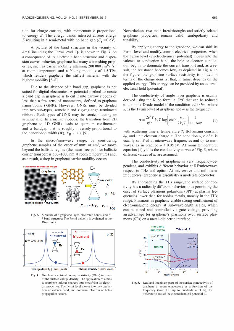
A picture of the band structure in the vicinity of k = 0 including the Fermi level EF is shown in Fig. 3. As a consequence of its electronic band structure and disper-sion curves behavior, graphene has many astonishing prop-erties, such as carrier mobility attaining 200 000 cm2V-1s-1
at room temperature and a Young modulus of 1.5 TPa, which renders graphene the stiffest material with the highest mobility [5–8].
Due to the absence of a band gap, graphene is not suited for digital electronics. A potential method to create a band gap in graphene is to cut it into narrow ribbons of less than a few tens of nanometers, defined as graphene nanoribbons ( GNR). However, GNRs must be divided into two sub-types, armchair and zig-zag edge terminated ribbons. Both types of GNR may be semiconducting or semimetallic. In armchair ribbons, the transition from 2D graphene to 1D GNRs leads to quantum confinement and a bandgap that is roughly inversely proportional to the nanoribbon width (W), Eg ~ 1/W [9].
In the micro-/mm-wave range, by considering graphene samples of the order of mm2 or cm2, we move beyond the ballistic regime (the mean-free path for ballistic carrier transport is 500–1000 nm at room temperature) and, as a result, a drop in graphene carrier mobility occurs.
Fig. 3. Structure of a graphene layer, electronic bonds, and E-
k band structure: The Fermi velocity is evaluated at the Dirac point.
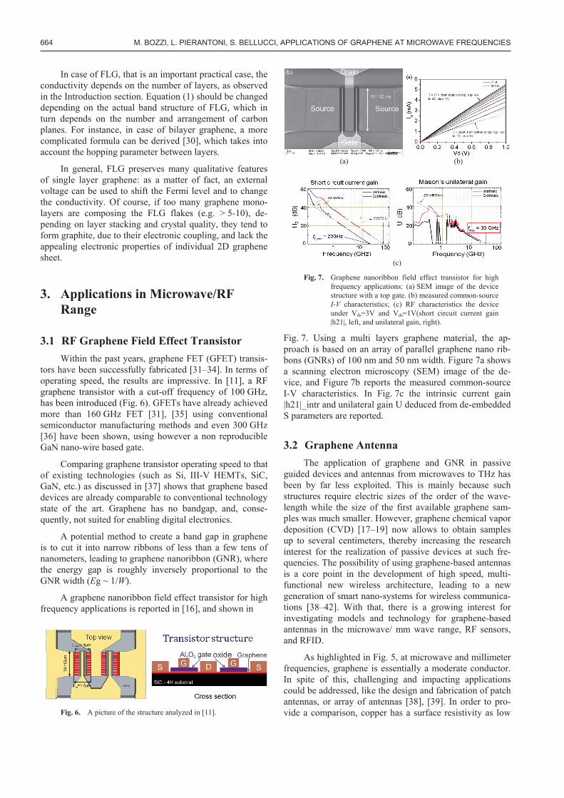
Fig. 4. Graphene electrical doping: resistivity (Ohm) in terms
of the surface charge density. The application of a bias to graphene induces charges thus modifying its electri-cal properties. The Fermi level moves into the conduc-tion or valence band, and dominant electron or holes propagation occurs.
Nevertheless, two main breakthroughs and strictly related graphene properties remain valid: ambipolarity and tunability.
By applying energy to the graphene, we can shift its Fermi level and modify/control electrical properties; when the Fermi level (electrochemical potential) moves into the valence or conduction band, the hole or electron conduc-tion begins to dominate the current transport and, as a re-sult, the resistance becomes low, as depicted in Fig. 4. In the figure, the graphene surface resistivity is plotted in terms of the charge density, that, in turns, depends on the applied energy. This energy can be provided by an external electrical field (potential).
The conductivity of single layer graphene is usually derived using the Kubo formula, [29] that can be reduced to a simple Drude model if the condition uc >> , where uc is the Fermi level of graphene and is the frequency:
ωτμ
πτσ
jTkTke
B
cB +
=1
12
coshlog22
2
(1)
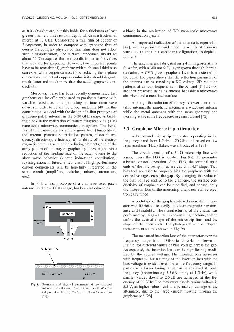
with scattering time , temperature T, Boltzmann constant kB, and unit electron charge e. The condition uc > > is usually satisfied at microwave frequencies and up to mm-waves, as in practice uc > 0.05 eV. At room temperature, equation (1) yields the conductivity curves of Fig. 5, where different values of uc are assumed.
The conductivity of graphene is very frequency-de-pendent, and exhibits different behavior at RF/microwave respect to THz and optics. At microwave and millimeter frequencies, graphene is essentially a moderate conductor.
By approaching the THz range, the surface conduc-tivity has a radically different behavior, thus permitting the onset of surface plasmons polaritons (SPP) at plasma fre-quencies lower than for nobles metals, namely in the THz range. Plasmons in graphene enable strong confinement of electromagnetic energy at sub-wavelength scales, which can be tuned and controlled via gate voltage, providing an advantage for graphene’s plasmons over surface plas-mons (SPs) on a metal–dielectric interface.
Fig. 5. Real and imaginary parts of the surface conductivity of
graphene at room temperature as a function of the frequency (from DC up to hundreds of THz), for different values of the electrochemical potential uc.
664 M. BOZZI, L. PIERANTONI, S. BELLUCCI, APPLICATIONS OF GRAPHENE AT MICROWAVE FREQUENCIES
In case of FLG, that is an important practical case, the conductivity depends on the number of layers, as observed in the Introduction section. Equation (1) should be changed depending on the actual band structure of FLG, which in turn depends on the number and arrangement of carbon planes. For instance, in case of bilayer graphene, a more complicated formula can be derived [30], which takes into account the hopping parameter between layers.
In general, FLG preserves many qualitative features of single layer graphene: as a matter of fact, an external voltage can be used to shift the Fermi level and to change the conductivity. Of course, if too many graphene mono-layers are composing the FLG flakes (e.g. > 5-10), de-pending on layer stacking and crystal quality, they tend to form graphite, due to their electronic coupling, and lack the appealing electronic properties of individual 2D graphene sheet.
3. Applications in Microwave/RF Range
3.1 RF Graphene Field Effect Transistor Within the past years, graphene FET (GFET) transis-
tors have been successfully fabricated [31–34]. In terms of operating speed, the results are impressive. In [11], a RF graphene transistor with a cut-off frequency of 100 GHz, has been introduced (Fig. 6). GFETs have already achieved more than 160 GHz FET [31], [35] using conventional semiconductor manufacturing methods and even 300 GHz [36] have been shown, using however a non reproducible GaN nano-wire based gate.
Comparing graphene transistor operating speed to that of existing technologies (such as Si, III-V HEMTs, SiC, GaN, etc.) as discussed in [37] shows that graphene based devices are already comparable to conventional technology state of the art. Graphene has no bandgap, and, conse-quently, not suited for enabling digital electronics.
A potential method to create a band gap in graphene is to cut it into narrow ribbons of less than a few tens of nanometers, leading to graphene nanoribbon (GNR), where the energy gap is roughly inversely proportional to the GNR width (Eg ~ 1/W).
A graphene nanoribbon field effect transistor for high frequency applications is reported in [16], and shown in
Fig. 6. A picture of the structure analyzed in [11].
(a) (b)
(c)
Fig. 7. Graphene nanoribbon field effect transistor for high frequency applications: (a) SEM image of the device structure with a top gate. (b) measured common-source I-V characteristics; (c) RF characteristics the device under Vds=3V and Vds=1V(short circuit current gain |h21|, left, and unilateral gain, right).
Fig. 7. Using a multi layers graphene material, the ap-proach is based on an array of parallel graphene nano rib-bons (GNRs) of 100 nm and 50 nm width. Figure 7a shows a scanning electron microscopy (SEM) image of the de-vice, and Figure 7b reports the measured common-source I-V characteristics. In Fig. 7c the intrinsic current gain |h21|_intr and unilateral gain U deduced from de-embedded S parameters are reported.
3.2 Graphene Antenna The application of graphene and GNR in passive
guided devices and antennas from microwaves to THz has been by far less exploited. This is mainly because such structures require electric sizes of the order of the wave-length while the size of the first available graphene sam-ples was much smaller. However, graphene chemical vapor deposition (CVD) [17–19] now allows to obtain samples up to several centimeters, thereby increasing the research interest for the realization of passive devices at such fre-quencies. The possibility of using graphene-based antennas is a core point in the development of high speed, multi-functional new wireless architecture, leading to a new generation of smart nano-systems for wireless communica-tions [38–42]. With that, there is a growing interest for investigating models and technology for graphene-based antennas in the microwave/ mm wave range, RF sensors, and RFID.
As highlighted in Fig. 5, at microwave and millimeter frequencies, graphene is essentially a moderate conductor. In spite of this, challenging and impacting applications could be addressed, like the design and fabrication of patch antennas, or array of antennas [38], [39]. In order to pro-vide a comparison, copper has a surface resistivity as low
RADIOENGINEERING, VOL. 24, NO. 3, SEPTEMBER 2015 665
as 0.03 Ohm/square, but this holds for a thickness at least greater than few times its skin depth, which is a fraction of micron at 13 GHz. Considering a thin film of copper of 3 Angstrom, in order to compare with graphene (but of course the complex physics of thin films does not allow such a simplification), the surface impedance should be about 60 Ohm/square, that not too dissimilar to the values that we used for graphene. However, two important points have to be remarked: i) graphene with such small thickness can exist, while copper cannot; ii) by reducing the in-plane dimensions, the actual copper conductivity should degrade much faster and much more than the actual graphene con-ductivity.
Moreover, it also has been recently demonstrated that graphene can be efficiently used as passive substrate with variable resistance, thus permitting to tune microwave devices in order to obtain the proper matching [40]. In this contribution, we deal with the design of a first prototype of graphene-patch antenna, in the 5-20 GHz range, as build-ing block in the realization of transmitting/receiving (T/R) nano-scale microwave communication system. The bene-fits of this nano-scale system are given by: i) tunability of the antenna parameters: radiation pattern, resonant fre-quency, directivity, efficiency; ii) tunability of the electro-magnetic coupling with other radiating elements, and of the array pattern of an array of graphene patches; iii) possible reduction of the in-plane size of the patch owing to the slow wave behavior (kinetic inductance contribution); iv) integration: in future, a new class of high performance carbon components will be hopefully integrated in the same circuit (amplifiers, switches, mixers, attenuators, etc.).
In [41], a first prototype of a graphene-based patch antenna, in the 5-20 GHz range, has been introduced as
Fig. 8. Geometry and physical parameters of the analyzed
antenna. W = 0.9 cm; L = 0.18 cm; S = 0.045 cm = 450 μm. A = 100 μm; B = 50 μm. H = 4.2 mm (from [42]).
a block in the realization of T/R nano-scale microwave communication system.
An improved realization of the antenna is reported in [42], with experimental and modeling results of a micro-wave slot antenna in a coplanar configuration, as depicted in Fig. 8.
The antennas are fabricated on a 4 in. high-resistivity Si wafer, with a 300 nm SiO2 layer grown through thermal oxidation. A CVD grown graphene layer is transferred on the SiO2. The paper shows that the reflection parameter of the antenna can be tuned by a DC voltage. 2D radiation patterns at various frequencies in the X band (8–12 GHz) are then presented using as antenna backside a microwave absorbent and a metalized surface.
Although the radiation efficiency is lower than a me-tallic antenna, the graphene antenna is a wideband antenna while the metal antennas with the same geometry and working at the same frequencies are narrowband [42].
3.3 Graphene Microstrip Attenuator A broadband microstrip attenuator, operating in the
frequency band from 1 GHz to 20 GHz and based on few layer graphene (FLG) flakes, was introduced in [28].
The circuit consists of a 50-Ω microstrip line with a gap, where the FLG is located (Fig. 9a). To guarantee a better contact deposition of the FLG, the terminal open ends of the microstrip lines are cut with 45° slope. Two bias tees are used to properly bias the graphene with the desired voltage across the gap. By changing the value of the bias voltage applied to the graphene, the surface con-ductivity of graphene can be modified, and consequently the insertion loss of the microstrip attenuator can be elec-tronically tuned.
A prototype of the graphene-based microstrip attenu-ator was fabricated to verify its electromagnetic perform-ance and tunability. The manufacturing of the circuit was performed by using a LPKF micro-milling machine, able to define the desired shape of the microstrip lines and the slope of the open ends. The photograph of the adopted measurement setup is shown in Fig. 9b.
The measured insertion loss of the attenuator over the frequency range from 1 GHz to 20 GHz is shown in Fig. 9c, for different values of bias voltage across the gap. As expected, the insertion loss can be significantly modi-fied by the applied voltage. The insertion loss increases with frequency, but a tuning of the insertion loss with the bias voltage is evident over the entire frequency range. In particular, a larger tuning range can be achieved at lower frequency (approximately 5.5 dB tuning at 1 GHz), while smaller values down to 2.5 dB are achieved at the fre-quency of 20 GHz. The maximum usable tuning voltage is 5.5 V, as higher values lead to a permanent damage of the attenuator, due to the large current flowing through the graphene pad [28].

666 M. BOZZI, L. PIERANTONI, S. BELLUCCI, APPLICATIONS OF GRAPHENE AT MICROWAVE FREQUENCIES
(a)
(b)
0
5
10
15
0 5 10 15 20
Inse
rtion
loss
(dB
)
Frequency (GHz)
V_DC=0
V_DC=4 V
V_DC=5 V
V_DC=5.5 V
(c)
Fig. 9. Graphene-based microstrip attenuator: (a) geometry of the measurement setup; (b) photograph of the proto-type in the measurement setup; (c) measured insertion loss vs. frequency, for different values of the bias volt-age (from [28]).
3.4 Graphene Composites in EM Shielding The application of graphene and GNR in electromag-
netic interference (EMI) shielding devices has a potential impact in electronics, automotive and aerospace sectors. Thus, it is important to investigate the effect of methods of preparation and concentration of graphene and the type of matrix on EMI shielding. The EMI shielding effectiveness (SE) of the obtained material cab is then analyzed, normally by a scalar network analyzer in the microwave
range to observe the percolation thresholds. Quite naturally the electromagnetic properties of the nanocomposites yield the basis for engineering and optimizing the shielding operation at the best achievable bandwidth, independently of the angle of incidence. Microstructure, elastic and elec-tromagnetic properties of epoxy-graphite composites filled with low percentages of exfoliated graphite and thick gra-phene was studied with the aid of the impulse acoustic microscopy technique [43]. The already mentioned tech-nique of FLG nanoplatelets fabrication was used for the realization of epoxy resin nanocomposites whose electrical properties were then studied [28].
Graphene is an interesting material also from the point of view of electromagnetic shielding. In particular, it now starts becoming clear that, thanks to its high electrical conductivity, a graphene plane yields a good shielding ef-ficiency against microwave radiation. When considered as a nanofiller, it yields several advantages with respect to other conventional nanofillers thanks to its large surface area, high aspect ratio, excellent thermal and electrical con-ductivity, as well as optimally high values of the elastic modulus. Furthermore, its flexibility and transparency provide another formidable asset. In [34] graphene was combined with poly(methyl methacrylate) (PMMA) to form sandwich structures composed of PMMA/graphene, where the CVD-obtained single-layered graphene was spin coated with a 600-800 nm thick PMMA layer. Also, the electromagnetic response of such heterostructures where graphene atomic planes alternate with polymer PMMA films were investigated [44]. Using thin polymer layers as spacers to separate several graphene planes allows one to arithmetically add the conductivities of each graphene plane, because, thanks to the isolating polymer layer, the intrinsic properties of each plane are kept. In this way, in [44] it was determined that, at 30 GHz, 6 is the optimum number of planes, as it corresponds to the maximum value in this microwave radiation absorption. Thanks to such a progress, the concept of electrically controlled graphene based electromagnetic composites is also rapidly advancing for the case of this kind of graphene/PMMA hetero-structures.
4. Conclusion Nano-technologies represent the new scenario for
electronics and photonics, and the application of carbon nano-electronics in the RF and microwave frequency range is receiving increasing attention.
This paper has presented an overview on the state-of-the-art in the applications of graphene at microwave fre-quencies. The basic features of carbon-based nanostruc-tures have been outlined and the emerging fabrication technologies have been discussed. Some recent achieve-ments in the field of graphene-based microwave compo-nents have been presented.
RADIOENGINEERING, VOL. 24, NO. 3, SEPTEMBER 2015 667
Acknowledgments
The authors wish to acknowledge partial support from the EU projects “NAmiceMC—Nano-thin and micro-sized carbons: Toward electromagnetic compatibility applica-tion”, “FAEMCAR—Fundamental and Applied Electro-magnetics of Nano-Carbons”, “Graphene-Based Revolu-tions in ICT and Beyond, GRAPHENE Flagship”, “Carbon Based Smart Systems for Wireless Application” (NANO-RF, n. 318352).
References [1] BENNETT, H. S., et al. Priorities for standards and measurements
to accelerate innovations in nano-electrotechnologies: Analysis of the NIST-energetics-IEC TC 113 survey. Journal of Research of the National Institutes of Standards and Technology, Apr. 2009, vol. 114, no. 2, p. 99–135. DOI: 10.6028/jres.114.008
[2] THOMPSON, S. E., PARTHASARATHY, S. Moore’s law: the future of Si microelectronics. Materials Today, June 2006, vol. 9, no. 6, p. 20–25. DOI: 10.1016/S1369-7021(06)71539-5
[3] RUSSER, P., FICHTNER, N. Nanoelectronics in radio-frequency technology. IEEE Microwave Magazine, May 2010, vol. 11, no. 3, p. 119–135. DOI: 10.1109/MMM.2010.936077
[4] PIERANTONI, L. RF nanotechnology - Concept, birth, mission and perspectives. IEEE Microwave Magazine, June 2010, vol. 11. no. 4, p. 130–137. DOI: 10.1109/MMM.2010.936485
[5] NOVOSELOV, S K. S., GEIM, A. K., MOROZOV, S. V., JIANG, D., ZHANG, Y., DUBONOS, S. V., GRIGORIEVA, I. V., FIRSOV, A. A. Electric field effect in atomically thin carbon films. Science, 2004, vol. 306, no. 5696, p. 666–669. DOI: 10.1126/science.1102896
[6] GEIM, A. K., NOVOSELOV, K. S. The rise of graphene. Arxiv preprint cond-mat/0702595, 2007.
[7] MOROZOV, S. V., et al. Giant intrinsic carrier mobilities in graphene and its bilayer. Physical Review Letters, 2008, vol. 100, no. 1, p. 16 602–16 605. DOI: 10.1103/PhysRevLett.100.016602
[8] BLAKE, P., HILL, E. W., CASTRO NETO, A. H., NOVOSELOV, K. S., JIANG, D., YANG, R., et al. Making graphene visible. Applied Physics Letters, 2007, vol. 91, 063124. DOI: 10.1063/1.2768624
[9] SON, Y.-W., COHEN, M. L., LOUIE, S. G. Energy gaps in graphene nanoribbons. Physical Review Letters, 2006, vol. 97, no. 21, p. 216803-4. DOI: 10.1103/PhysRevLett.97.216803
[10] PIERANTONI, L., COCCETTI, F., RUSSER, P. Nanoelectronics: The paradigm shift. IEEE Microwave Magazine, Dec. 2010, vol. 11, no. 17, p. 8–10. DOI: 10.1109/MMM.2010.938552
[11] LIN, Y. M., JENKINS, K. A., VALDES-GARCIA, A., SMALL, J. P., FARMER, D. B., AVOURIS, P. Operation of graphene transistors at gigahertz frequencies. Nano Letters, 2009, vol. 9, p. 422–426. DOI: 10.1021/nl803316h
[12] WANG, H., NEZICH, D., JING KONG, D., PALACIOS, T. Graphene frequency multipliers. IEEE Electron Device Letters, 2009, vol. 30, p. 547–549. DOI: 10.1109/LED.2009.2016443
[13] WANG, X., ZHI, L., MULLEN, K. Transparent, conductive graphene electrodes for dye-sensitized solar cells. Nano Letters, 2008, no. 8, p. 323–327. DOI: 10.1021/nl072838r
[14] VAKIL, A., ENGHETA, N. Transformation optics using graphene. Science, 2011, vol. 332, no. 6035, p. 1291–1294. DOI: 10.1126/science.1202691
[15] JABLAN, M., BULJAN, H., SOLJACIC, M. Plasmonics in graphene infrared frequencies. Physical Review B, 2009, vol. 80, p. 1–7. DOI: 10.1103/PhysRevB.80.245435
[16] MENG, J. N., FERNANDEZ, J. F., PICHONAT, E., LANCRY, O., VIGNAUD, D., DAMBRINE, G., HAPPY, H. RF characterization of epitaxial graphene nano ribbon field effect transistor. In IEEE MTT-S International Microwave Symposium Digest. Baltimore (MD, USA), June 2011, p. 1–3. DOI: 10.1109/MWSYM.2011.5972627
[17] OBRAZTSOV, A. N., et al. Chemical vapor deposition of thin graphite films of nanometer thickness. Carbon, 2007, vol. 45, no. 10, p. 2017–2021. DOI:10.1016/j.carbon.2007.05.028
[18] YU, Q., et al. Graphene segregated on Ni surfaces and transferred to insulators. Applied Physics Letters, 2008, vol. 93, no. 11, p. 113103-3. DOI:10.1063/1.2982585
[19] MALESEVIC, A., et al. Synthesis of few-layer graphene via microwave plasma-enhanced chemical vapour deposition. Nanotechnology, 2008, vol. 19, 305604. DOI: 10.1088/0957-4484/19/30/305604
[20] BELLUCCI, S., MALESEVIC, A. Physics of carbon nanostruc-tures. In Physical Properties of Ceramic and Carbon Nanoscale Structures Lecture Notes in Nanoscale Science and Technology 11, Springer: Berlin Heidelberg, 2011. ISBN 978-3-642-15778-3
[21] BELLUCCI, S., et al. Comparative field emission from vertically aligned few-layer graphene and carbon nanotubes. Nanoscience and Nanotechnology Letters, 2011, vol. 3, p. 907–912. DOI: 10.1166/nnl.2011.1253
[22] YAN, K., FU, L., PENG, H., LIU, Z. Designed CVD growth of graphene via process engineering. Accounts of Chemical Research, 2013, vol. 46, p. 2263–2274. DOI: 10.1021/ar400057n
[23] CAO, H., et al. Electronic transport in chemical vapor deposited graphene synthesized on Cu: Quantum Hall effect and weak localization. Applied Physics Letters, 2010, vol. 96, 122106. DOI: 10.1063/1.3371684
[24] BABICHEV, A.V., et al. Contact properties to CVD-graphene on GaAs substrates for optoelectronic applications. Nanotechnology, 2014, vol. 25, 335707. DOI: 10.1088/0957-4484/25/33/335707
[25] MAFFUCCI, A., MICCIULLA, F., CATALDO, A., MIANO, G., BELLUCCI, S. Synthesis and electrical characterization of graphene nanoplatelets. In International Conference on Electromagnetics in Advanced Applications (ICEAA2015). Turin (Italy), 2015.
[26] MAFFUCCI, A., MICCIULLA, F., CATALDO, A., MIANO, G., BELLUCCI, S. Bottom-up realization and electrical characterization of a graphene-based device. Submitted to Nanotechnology, 2015.
[27] DABROWSKA, A., BELLUCCI, S., CATALDO, A., MICCIULLA, F., HUCZKO, A. Nanocomposites of epoxy resin with graphene nanoplates and exfoliated graphite: Synthesis and electrical properties. Physica Status Solidi B, 2014, vol. 251, no. 12, p. 2599–2602. DOI: 10.1002/pssb.201451175
[28] PIERANTONI, L., MENCARELLI, D., BOZZI, M., MORO, R., MOSCATO, S., PERREGRINI, L., MICCIULLA, F., CATALDO, A., BELLUCCI, S. Broadband microwave attenuator based on few layer graphene flakes. IEEE Transactions on Microwave Theory and Techniques, Aug. 2015, vol. 63, no. 8, p. 2491–2497. DOI: 10.1109/TMTT.2015.2441062
[29] HANSON, G. W. Dyadic Greens functions and guided surface waves for a surface conductivity of graphene. Journal of Applied Physics, 2008, vol. 103, 064302. DOI: 10.1063/1.2891452
668 M. BOZZI, L. PIERANTONI, S. BELLUCCI, APPLICATIONS OF GRAPHENE AT MICROWAVE FREQUENCIES
[30] HWANG, J., CARBOTTE, J. P., TONGAY, S., HEBARD, A. F., TANNER, D. B. Ultrapure multilayer graphene in bromine-intercalated graphite. Physical Review B, 2011, vol. 84, 041410. DOI: 10.1103/PhysRevB.84.041410
[31] XING, C.J., et al. Investigation on self-heating effect in carbon nanotubes field-effect transistors. IEEE Transactions on Electron Devices, 2010, vol. 58, no. 2, p. 523–529. DOI: 10.1109/TED.2010.2090528
[32] KIM, S., CHOI, T.-Y., SHIM, M., MOHAMMADI, S. A poly-Si gate carbon nanotube field effect transistor for high frequency applications. In IEEE MTT-S International Microwave Symposium Digest. June 2005. DOI: 10.1109/MWSYM.2005.1516586
[33] KOCABAS, C., et al. High-frequency performance of submicro-meter transistors that use aligned arrays of single-walled carbon nanotubes. Nano Letters, 2009, vol. 9, no. 5, p.1937–1943. DOI: 10.1021/nl9001074
[34] LE LOUARN, A., et al. Intrinsic current gain cutoff frequency of 30 GHz with CNT transistors. Applied Physics Letters, 2007, vol. 90, 233108. DOI: 10.1063/1.2743402
[35] KESHAVARZI, A., et al. Carbon nanotube field-effect transistors for high-performance digital circuits; transient analysis, parasitics, and scalability. IEEE Transactions on Electron Devices, 2006, vol. 53, no. 11, p. 2718–2726. DOI: 10.1109/TED.2006.883813
[36] PESETSKI, A., et al. Carbon nanotube field-effect transistor operation at microwave frequencies. Applied Physics Letters, 2006, vol. 88, 113103. DOI: 10.1063/1.2185007
[37] BOURGOIN, J. P., et al. Directed assembly for carbon nanotube device fabrication. In International Electron Devices Meeting (IEDM 2006). San Francisco (USA), 2006. DOI: 10.1109/IEDM.2006.346805
[38] LLATSER, I., et al. Graphene-based nano-patch antenna for terahertz radiation. Photonics and Nanostructures, 2012, vol. 10, no. 4, p. 353–358. DOI: 10.1016/j.photonics.2012.05.011
[39] GOMEZ-DIAZ, J. S., PERRUISSEAU-CARRIER, J. Microwave to THz properties of graphene and potential antenna applications. In International Symposium on Antennas and Propagation (ISAP2012). Nagoya (Japan), 2012, p. 239-242.
[40] DRAGOMAN, M., et al. Terahertz antenna based on graphene. Journal of Applied Physics, 2010, vol. 107, 104313. DOI: 10.1063/1.3427536
[41] MENCARELLI, D., DRAGOMAN, M., PIERANTONI, L., ROZZI, T., COCCETTI, F. Design of a coplanar graphene-based nano-patch antenna for microwave applications. In International Microwave Symposium (IMS), Microwave Symposium Digest (MTT). Seattle (WA, USA), June 2013, p. 1–4. DOI: 10.1109/MWSYM.2013.6697800
[42] DRAGOMAN, M., NECULOIU,, D., BUNEA, A.-C., DELIGEORGIS, G., ALDRIGO, M., VASILACHE, D., DINESCU, A., KONSTANTINIDIS, G., MENCARELLI, D., PIERANTONI, L., MODREANU, M. A tunable microwave slot antenna based on graphene. Applied Physics Letters, April 2015, vol. 106, no. 15, 153101. DOI: 10.1063/1.4917564
[43] BELLUCCI, S., MICCIULLA, F., LEVIN, V. M., PETRONYUK, YU. S., CHERNOZATONSKII, L. A., KUZHIR, P. P., PADDUBSKAYA, A. G., MACUTKEVIC, J., PLETNEV, M. A., FIERRO, V., CELZARD, A. Microstructure, elastic and electromagnetic properties of epoxy-graphite composites. AIP Advances, 2015, vol. 5, 067137. DOI: 10.1063/1.4922872
[44] BATRAKOV, K., KUZHIR, P., MAKSIMENKO, S., PADDUB-SKAYA, A., VORONOVICH, S., LAMBIN, PH., KAPLAS, T., SVIRKO, YU. Flexible transparent graphene/polymer multilayers for efficient electromagnetic field absorption. Scientific Reports, 2014, vol. 4, 7191. DOI: 10.1038/srep07191
About the Authors ... Maurizio BOZZI was born in Voghera, Italy, in 1971. He received the Ph.D. degree in Electronics and Computer Science from the University of Pavia, Pavia, Italy, in 2000. He held research positions with various universities world-wide, including the Technische Universität Darmstadt, Darmstadt, Germany; the Universitat de Valencia, Valen-cia, Spain; and the École Polytechnique de Montréal, Montreal, QC, Canada. In 2002, he joined the Department of Electronics, University of Pavia, where he is currently an Associate Professor. He has authored or co-authored more than 80 journal papers and 220 conference papers. He co-edited the book Periodic Structures (Research Signpost, 2006) and co-authored the book Microstrip Lines and Slot-lines (Artech House, 2013). His main research interests concern the development of numerical methods for the electromagnetic modeling and design of microwave and millimeter-wave components with a particular focus on frequency-selective surfaces and substrate integrated wave-guides. Prof. Bozzi was the General Conference Chair of the IEEE International Conference on Numerical Elec-tromagnetic Modeling and Optimization (NEMO2014), Pavia, Italy, 2014, and the General Chair of the IEEE MTT-S International Microwave Workshop Series on Millimeter Wave Integration Technologies, Sitges, Spain, 2011. He is a member of the Publication Committee and of the Education Committee of the IEEE MTT-S and of the General Assembly (GA) of the European Microwave As-sociation (EuMA) for the 2014–2016 term. He is an asso-ciate editor for IEEE Microwave and Wireless Components Letters, IET Microwaves, Antennas and Propagation, and IET Electronics Letters. He received several awards, in-cluding the 2015 Premium Award for Best Paper in IET Microwaves, Antennas & Propagation, the 2014 Premium Award for the Best Paper in Electronics Letters, the Best Young Scientist Paper Award of the XXVII General As-sembly of URSI in 2002, and the MECSA Prize at the Italian Conference on Electromagnetics (RiNEm) in 2000.
Luca PIERANTONI received the ‘Laurea’ degree (summa cum laude) in Electronics Engineering in 1988 and the Ph.D. degree in 1993 in Electromagnetics from the Uni-versity of Ancona, Italy. From 1996 to 2000 he worked at the Technical University of Munich, Germany, in the In-stitute of High-Frequency Engineering as Senior Research Scientist. In 2000 he joined the Polytechnic University of Marche, Ancona, Italy. Presently, he is a Professor at the Department of Information Technology of the Polytechnic University of Marche, Ancona, Italy. In 2014, he received by Italy Ministry of University the habilitation as Full Professor in Electromagnetic Fields. His current research interests are in the i) investigation of the combined elec-tromagnetic-quantum transport phenomena in nano-struc-tured materials/devices, ii) analysis of quantum electrody-namics in nanostructures, iii) development of computa-tional techniques and numerical tools for the multiphysics modeling of nano-scale devices, including quantum trans-port, electromagnetics, opto-mechanics, thermal diffusion,

RADIOENGINEERING, VOL. 24, NO. 3, SEPTEMBER 2015 669
opto-mechanics, opto-electronics, non-linear effects. He has been the co-founder and the first Chair of the IEEE MTT-25 “RF Nanotechnology” Technical Committee of the Microwave Theory and Technique Society (MTT-S). Awards: IEEE Distinguished Microwave Lecturer Emeritus (DML-E), 2015; IEEE Distinguished Microwave Lecturer (DML), 2012-2014; IEEE Nanotechnology Council Distin-guished Lecturer (NTC-DL), 2015-2016; EuMA European Microwave Lecturer (EML). Member of the IEEE Nanotech-nology Council (NTC) AdCom. Member of the Italian In-stitute of Nuclear Physics (INFN). Associate Editor of the IEEE Transaction on Nanotechnology (T-NANO) and of the IEEE Nanotechnology Express (ENANO) Letters. Member of the International Microwave Symposium Tech-nical Paper Review Committee (IMS TPRC). Stefano BELLUCCI was born in Rome. He received his M.Sc. (summa cum laude) from the University of Rome Sapienza in 1982. He received his Ph.D. in Physics of Elementary Particles from the International School for Advanced Studies at Trieste in 1986. He worked as Re-search Associate at Brandeis Univ., Waltham, MA, USA (1983-1985); as visiting researcher at M.I.T., Cambridge, MA, USA (1985-1986), at Univ. of Maryland, USA (1986-1987), at Univ. of California at Davis, USA (1987-1988).
He was appointed as a Tenured Researcher (Research Staff) at INFN (Istituto Nazionale di Fisica Nucleare) La-boratori Nazionali di Frascati (LNF) in 1987. He was ap-pointed as INFN First Researcher (Senior Research Staff) in 2005. He received by Italy Ministry of University in 2013 the habilitation as Full Professor in Theoretical Physics of Fundamental Interactions and the habilitation as Full Professor in Theoretical Condensed Matter Physics. His research interests include theoretical physics, con-densed matter, nanoscience and nanotechnology, nanocar-bon based composites, biomedical applications. He pub-lished over 500 papers in peer-reviewed journals with h = 45, and more than 10 invited book chapters. He is the Edi-tor and/or co-author of 10 books with Springer. He appears in the list of Top Italian Scientists published by the VIA Academy. He received the B.W. Lee Prize at Erice School of Subnuclear Physics (Erice, Italy) 1982. In 1980 he was selected as Summer student at CERN (Geneva). He is Se-ries Editor of Springer Lecture Notes in Nanoscale Science and Technology, and Editorial Board Member of the Jour-nal of Nanomaterials. He is Director of the NATO Emerg-ing Security Challenges Division, SPS Programme project “Development of Biosensors using Carbon Nanotubes” and INFN scientist in charge of several Italian and EU projects.