Embed Size (px)
Citation preview
Application-Specific Accelerators forCommunications
Yang Sun, Kiarash Amiri, Michael Brogioli, and Joseph R. Cavallaro
Abstract For computation-intensive digital signal processing algorithms, complex-ity is exceeding the processing capabilities of general-purpose digital signal proces-sors (DSPs). In some of these applications, DSP hardware accelerators have beenwidely used to off-load a variety of algorithms from the main DSP host, includingFFT, FIR/IIR filters, multiple-input multiple-output (MIMO) detectors, and errorcorrection codes (Viterbi, Turbo, LDPC) decoders. Given power and cost consid-erations, simply implementing these computationally complex parallel algorithmswith high-speed general-purpose DSP processor is not very efficient. However, notall DSP algorithms are appropriate for off-loading to a hardware accelerator. First,these algorithms should have data-parallel computations and repeated operationsthat are amenable to hardware implementation. Second, these algorithms shouldhave a deterministic dataflow graph that maps to parallel datapaths. The acceleratorsthat we consider are mostly coarse grain to better deal with streaming data transferfor achieving both high performance and low power. In this chapter, we focus onsome of the basic and advanced digital signal processing algorithms for communi-cations and cover major examples of DSP accelerators for communications.
Yang SunRice University, 6100 Main St., Houston, TX 77005, e-mail: [email protected]
Kiarash AmiriRice University, 6100 Main St., Houston, TX 77005, e-mail: [email protected]
Michael BrogioliFreescale Semiconductor Inc., 7700 W. Parmer Lane, MD: PL63, Austin TX 78729,e-mail: [email protected]
Joseph R. CavallaroRice University, 6100 Main St., Houston, TX 77005, e-mail: [email protected]
329S.S. Bhattacharyya et al. (eds.), Handbook of Signal Processing Systems,DOI 10.1007/978-1-4419-6345-1_13, © Springer Science+Business Media, LLC 2010
330 Yang Sun, Kiarash Amiri, Michael Brogioli, and Joseph R. Cavallaro
1 Introduction
In third-generation (3G) wireless systems, the signal processing algorithm complex-ity has begun to exceed the processing capabilities of general purpose digital signalprocessors (DSPs). With the inclusion of multiple-input multiple-output (MIMO)technology in the fourth-generation (4G) wireless system, the DSP algorithm com-plexity has far exceeded the processing capabilities of DSPs. Given area and powerconstraints for the mobile handsets one can not simply implement computation in-tensive DSP algorithms with gigahertz DSPs. Besides, it is also critical to reducebase station power consumption by utilizing optimized hardware accelerator design.Fortunately, only a few DSP algorithms dominate the main computational complex-ity in a wireless receiver. These algorithms, including Viterbi decoding, Turbo de-coding, LDPC decoding, MIMO detection, and channel equalization/FFT, need tobe off-loaded to hardware coprocessors or accelerators, yielding high performance.These hardware accelerators are often integrated in the same die with DSP proces-sors. In addition, it is also possible to leverage the field-programmable gate array(FPGA) to provide reconfigurable massive computation capabilities.
DSP workloads are typically numerically intensive with large amounts of bothinstruction and data level parallelism. In order to exploit this parallelism with a pro-grammable processor, most DSP architectures utilize Very Long Instruction Word,or VLIW architectures. VLIW architectures typically include one or more regis-ter files on the processor die, versus a single monolithic register file as is oftenthe case in general purpose computing. Examples of such architectures are theFreescale StarCore processor, the Texas Instruments TMS320C6x series DSPs aswell as SHARC DSPs from Analog Devices, to name a few [14, 28, 39].
In some cases due to the idiosyncratic nature of many DSPs, and the imple-mentation of some of the more powerful instructions in the DSP core, an optimizingcompiler can not always target core functionality in an optimal manner. Examples ofthis include high performance fractional arithmetic instructions, for example, whichmay perform highly SIMD functionality which the compiler can not always deemsafe at compile time.
While the aforementioned VLIW based DSP architectures provide increased par-allelism and higher numerical throughput performance, this comes at a cost of easein programmability. Typically such machines are dependent on advanced optimizingcompilers that are capable of aggressively analyzing the instruction and data levelparallelism in the target workloads, and mapping it onto the parallel hardware. Dueto the large number of parallel functional units and deep pipeline depths, modernDSP are often difficult to hand program at the assembly level while achieving opti-mal results. As such, one technique used by the optimizing compiler is to vectorizemuch of the data level parallelism often found in DSP workloads. In doing this,the compiler can often fully exploit the single instruction multiple data, or SIMDfunctionality found in modern DSP instruction sets.
Despite such highly parallel programmable processor cores and advanced com-piler technology, however, it is quite often the case that the amount of availableinstruction and data level parallelism in modern signal processing workloads far
Application-Specific Accelerators for Communications 331
exceeds the limited resources available in a VLIW based programmable processorcore. For example, the implementation complexity for a 40 Kbps DS-CDMA sys-tem would be 41.8 Gflops/s for 60 users [50], not to mention 100 Mbps+ 3GPPLTE system. This complexity largely exceeds the capability of nowadays DSP pro-cessors which typically can provide 1-5 Gflops performance, such as 1.5 Gflops TIC6711 DSP processor and 1.8 Gflops ADI TigerSHARC Processor. In other cases,the functionality required by the workload is not efficiently supported by more gen-eral purpose instruction sets typically found in embedded systems. As such the needfor acceleration at both the fine grain and coarse grain levels is often required, theformer for instruction set architecture (ISA) like optimization and the latter for tasklike optimization.
Additionally, wireless system designers often desire the programmability offeredby software running on a DSP core versus a hardware based accelerator, to allowflexibility in various proprietary algorithms. Examples of this can be functionalitysuch as channel estimation in baseband processing, for which a given vendor maywant to use their own algorithm to handle various users in varying system conditionsversus a pre-packaged solution. Typically these demands result in a heterogeneoussystem which may include one or more of the following: software programmableDSP cores for data processing, hardware based accelerator engines for data pro-cessing, and in some instances general purpose processors or micro-controller typesolutions for control processing.
The motivations for heterogeneous DSP system solutions including hardware ac-celeration stem from the tradeoffs between software programmability versus theperformance gains of custom hardware acceleration in its various forms. There area number of heterogenous accelerator based architectures currently available today,as well as various offerings and design solutions being offered by the research com-munity.
There are a number of DSP architectures which include true hardware based ac-celerators which are not programmable by the end user. Examples of this include theTexas Instruments’ C55x and C64x series of DSPs which include hardware basedViterbi or Turbo decoder accelerators for acceleration of wireless channel decod-ing [26, 27].
1.1 Coarse Grain Versus Fine Grain Accelerator Architectures
Coarse–grain accelerator based DSP systems entail a co–processor type designwhereby larger amounts of work are run on the sometimes configurable co–processordevice. Current technologies being offered in this area support offloading of func-tionality such as FFT and various matrix-like computations to the accelerator versusexecuting in software on the programmable DSP core.
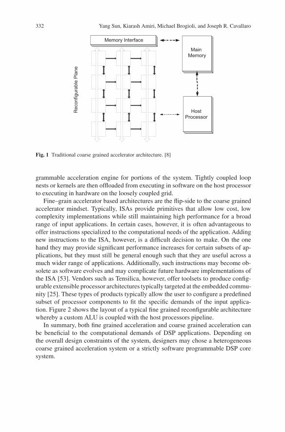
As shown in Figure 1, coarse grained heterogeneous architectures typically in-clude a loosely coupled computational grid attached to the host processor. Thesetypes of architectures are sometimes built using an FPGA, ASIC, or vendor pro-
332 Yang Sun, Kiarash Amiri, Michael Brogioli, and Joseph R. Cavallaro
Memory Interface
HostProcessor
Main Memory
Rec
onfig
urab
le P
lane
Fig. 1 Traditional coarse grained accelerator architecture. [8]
grammable acceleration engine for portions of the system. Tightly coupled loopnests or kernels are then offloaded from executing in software on the host processorto executing in hardware on the loosely coupled grid.
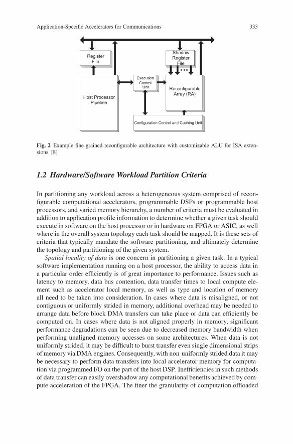
Fine–grain accelerator based architectures are the flip-side to the coarse grainedaccelerator mindset. Typically, ISAs provide primitives that allow low cost, lowcomplexity implementations while still maintaining high performance for a broadrange of input applications. In certain cases, however, it is often advantageous tooffer instructions specialized to the computational needs of the application. Addingnew instructions to the ISA, however, is a difficult decision to make. On the onehand they may provide significant performance increases for certain subsets of ap-plications, but they must still be general enough such that they are useful across amuch wider range of applications. Additionally, such instructions may become ob-solete as software evolves and may complicate future hardware implementations ofthe ISA [53]. Vendors such as Tensilica, however, offer toolsets to produce config-urable extensible processor architectures typically targeted at the embedded commu-nity [25]. These types of products typically allow the user to configure a predefinedsubset of processor components to fit the specific demands of the input applica-tion. Figure 2 shows the layout of a typical fine grained reconfigurable architecturewhereby a custom ALU is coupled with the host processors pipeline.
In summary, both fine grained acceleration and coarse grained acceleration canbe beneficial to the computational demands of DSP applications. Depending onthe overall design constraints of the system, designers may chose a heterogeneouscoarse grained acceleration system or a strictly software programmable DSP coresystem.
Application-Specific Accelerators for Communications 333
Host ProcessorPipeline
RegisterFile
ShadowRegister
File
ReconfigurableArray (RA)
Execution Control
Unit
Configuration Control and Caching Unit
Fig. 2 Example fine grained reconfigurable architecture with customizable ALU for ISA exten-sions. [8]
1.2 Hardware/Software Workload Partition Criteria
In partitioning any workload across a heterogeneous system comprised of recon-figurable computational accelerators, programmable DSPs or programmable hostprocessors, and varied memory hierarchy, a number of criteria must be evaluated inaddition to application profile information to determine whether a given task shouldexecute in software on the host processor or in hardware on FPGA or ASIC, as wellwhere in the overall system topology each task should be mapped. It is these sets ofcriteria that typically mandate the software partitioning, and ultimately determinethe topology and partitioning of the given system.
Spatial locality of data is one concern in partitioning a given task. In a typicalsoftware implementation running on a host processor, the ability to access data ina particular order efficiently is of great importance to performance. Issues such aslatency to memory, data bus contention, data transfer times to local compute ele-ment such as accelerator local memory, as well as type and location of memoryall need to be taken into consideration. In cases where data is misaligned, or notcontiguous or uniformly strided in memory, additional overhead may be needed toarrange data before block DMA transfers can take place or data can efficiently becomputed on. In cases where data is not aligned properly in memory, significantperformance degradations can be seen due to decreased memory bandwidth whenperforming unaligned memory accesses on some architectures. When data is notuniformly strided, it may be difficult to burst transfer even single dimensional stripsof memory via DMA engines. Consequently, with non-uniformly strided data it maybe necessary to perform data transfers into local accelerator memory for computa-tion via programmed I/O on the part of the host DSP. Inefficiencies in such methodsof data transfer can easily overshadow any computational benefits achieved by com-pute acceleration of the FPGA. The finer the granularity of computation offloaded
334 Yang Sun, Kiarash Amiri, Michael Brogioli, and Joseph R. Cavallaro
for acceleration in terms of compute time, quite often the more pronounced the sideeffects of data memory transfer to local accelerator memory.
Data level parallelism is another important criteria in determining the partition-ing for a given application. Many applications targeted at VLIW-like architectures,especially signal processing applications, exhibit a large amount of both instructionand data level parallelism [24]. Many signal processing applications often containenough data level parallelism to exceed the available functional units of a givenarchitecture. FPGA fabrics and highly parallel ASIC implementations can exploitthese computational bottlenecks in the input application by providing not only largenumbers of functional units but also large amounts of local block data RAM to sup-port very high levels of instruction and data parallelism, far beyond that of what atypical VLIW signal processing architecture can afford in terms of register file realestate. Furthermore, depending on the instruction set architecture of the host proces-sor or DSP, performing sub-word or multiword operations may not be feasible giventhe host machine architecture. Most modern DSP architecures have fairly robust in-struction sets that support fine grained multiword SIMD acceleration to a certainextent. It is often challenging, however, to efficiently load data from memory intothe register files of a programmable SIMD style processor to be able to efficientlyor optimally utilize the SIMD ISA in some cases.
Computational complexity of the application often bounds the programmableDSP core, creating a compute bottleneck in the system. Algorithms that are im-plemented in FPGA are often computationally intensive, exploiting greater amountsof instruction and data level parallelism than the host processor can afford, giventhe functional unit limitations and pipeline depth. By mapping computationally in-tense bottlenecks in the application from software implementation executing on hostprocessor to hardware implementation in FPGA, one can effectively alleviate bot-tlenecks on the host processor and permit extra cycles for additional computation oralgorithms to execute in parallel.
Task level parallelism in a portion of the application can play a role in the idealpartitioning as well. Quite often, embedded applications contain multiple tasks thatcan execute concurrently, but have a limited amount of instruction or data level par-allelism within each unique task [51]. Applications in the networking space, andbaseband processing at layers above the data plane typically need to deal with pro-cessing packets and traversing packet headers, data descriptors and multiple taskqueues. If the given task contains enough instruction and data level parallelism toexhaust the available host processor compute resources, it can be considered forpartitioning to an accelerator. In many cases, it is possible to concurrently executemultiple of these tasks in parallel, either across multiple host processors or acrossboth host processor and FPGA compute engine depending on data access patternsand cross task data dependencies. There are a number of architectures which haveaccelerated tasks in the control plane, versus data plane, in hardware. One exampleof this is the Freescale Semiconductor QorIQ platform which provides hardware ac-celeration for frame managers, queue managers and buffer managers. In doing this,the architecture effectively frees the programmable processor cores from dealingwith control plane management.
Application-Specific Accelerators for Communications 335
MIMO Encoder
... MIMO Detector
... Channel Decoder
MIMO Equalizer & Estimator
...
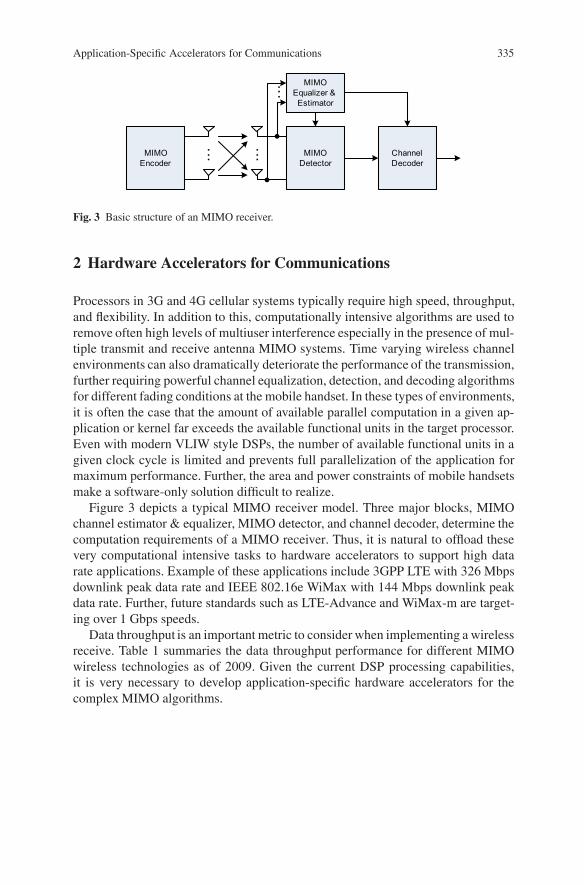
Fig. 3 Basic structure of an MIMO receiver.
2 Hardware Accelerators for Communications
Processors in 3G and 4G cellular systems typically require high speed, throughput,and flexibility. In addition to this, computationally intensive algorithms are used toremove often high levels of multiuser interference especially in the presence of mul-tiple transmit and receive antenna MIMO systems. Time varying wireless channelenvironments can also dramatically deteriorate the performance of the transmission,further requiring powerful channel equalization, detection, and decoding algorithmsfor different fading conditions at the mobile handset. In these types of environments,it is often the case that the amount of available parallel computation in a given ap-plication or kernel far exceeds the available functional units in the target processor.Even with modern VLIW style DSPs, the number of available functional units in agiven clock cycle is limited and prevents full parallelization of the application formaximum performance. Further, the area and power constraints of mobile handsetsmake a software-only solution difficult to realize.
Figure 3 depicts a typical MIMO receiver model. Three major blocks, MIMOchannel estimator & equalizer, MIMO detector, and channel decoder, determine thecomputation requirements of a MIMO receiver. Thus, it is natural to offload thesevery computational intensive tasks to hardware accelerators to support high datarate applications. Example of these applications include 3GPP LTE with 326 Mbpsdownlink peak data rate and IEEE 802.16e WiMax with 144 Mbps downlink peakdata rate. Further, future standards such as LTE-Advance and WiMax-m are target-ing over 1 Gbps speeds.
Data throughput is an important metric to consider when implementing a wirelessreceive. Table 1 summaries the data throughput performance for different MIMOwireless technologies as of 2009. Given the current DSP processing capabilities,it is very necessary to develop application-specific hardware accelerators for thecomplex MIMO algorithms.
336 Yang Sun, Kiarash Amiri, Michael Brogioli, and Joseph R. Cavallaro
Table 1 Throughput performance of different MIMO systems
HSDPA+ LTE LTE WiMax Rel 1.5 WiMax Rel 1.5(2×2 MIMO) (2×2 MIMO) (4×4 MIMO) (2×2 MIMO) (4×4 MIMO)
Downlink 42 Mbps 173 Mbps 326 Mbps 144 Mbps 289 MbpsUplink 11.5 Mbps 58 Mbps 86 Mbps 69 Mbps 69 Mbps
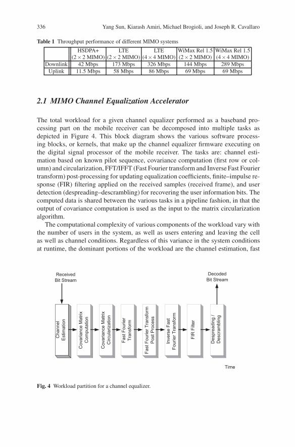
2.1 MIMO Channel Equalization Accelerator
The total workload for a given channel equalizer performed as a baseband pro-cessing part on the mobile receiver can be decomposed into multiple tasks asdepicted in Figure 4. This block diagram shows the various software process-ing blocks, or kernels, that make up the channel equalizer firmware executing onthe digital signal processor of the mobile receiver. The tasks are: channel esti-mation based on known pilot sequence, covariance computation (first row or col-umn) and circularization, FFT/IFFT (Fast Fourier transform and Inverse Fast Fouriertransform) post-processing for updating equalization coefficients, finite–impulse re-sponse (FIR) filtering applied on the received samples (received frame), and userdetection (despreading–descrambling) for recovering the user information bits. Thecomputed data is shared between the various tasks in a pipeline fashion, in that theoutput of covariance computation is used as the input to the matrix circularizationalgorithm.
The computational complexity of various components of the workload vary withthe number of users in the system, as well as users entering and leaving the cellas well as channel conditions. Regardless of this variance in the system conditionsat runtime, the dominant portions of the workload are the channel estimation, fast
Time
`
DecodedBit Stream
ReceivedBit Stream
Cha
nnel
Est
imat
ion
Cov
aria
nce
Mat
rixC
ompu
tatio
n
Cov
aria
nce
Mat
rixC
ircul
ariz
atio
n
Fast
Fou
rier
Tran
sfor
m
Fast
Fou
rier T
rans
form
Pos
t Pro
cess
Inve
rse
Fast
Four
ier T
rans
form
FIR
Filt
er
Des
prea
ding
/D
escr
ambl
ing
Fig. 4 Workload partition for a channel equalizer.
Application-Specific Accelerators for Communications 337
`
DSP
FPGA
Ch
an
ne
l
Es
tim
ati
on
Ch
an
ne
l
Es
tim
ati
on
Ch
an
ne
l
Es
tim
ati
on
Co
va
ria
nc
e M
atr
ix
Co
mp
uta
tio
nF
FT
Po
st
FF
T
Pro
ce
ss
ing
IFF
T
FIR
Fil
terin
g
Desp
read
Descram
ble
ReceivedSequence
DecodedSequence
Fig. 5 Channel equalizer DSP/hardware accelerator partitioning.
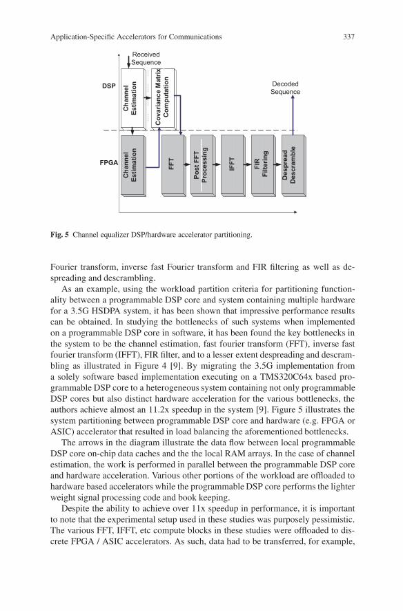
Fourier transform, inverse fast Fourier transform and FIR filtering as well as de-spreading and descrambling.
As an example, using the workload partition criteria for partitioning function-ality between a programmable DSP core and system containing multiple hardwarefor a 3.5G HSDPA system, it has been shown that impressive performance resultscan be obtained. In studying the bottlenecks of such systems when implementedon a programmable DSP core in software, it has been found the key bottlenecks inthe system to be the channel estimation, fast fourier transform (FFT), inverse fastfourier transform (IFFT), FIR filter, and to a lesser extent despreading and descram-bling as illustrated in Figure 4 [9]. By migrating the 3.5G implementation froma solely software based implementation executing on a TMS320C64x based pro-grammable DSP core to a heterogeneous system containing not only programmableDSP cores but also distinct hardware acceleration for the various bottlenecks, theauthors achieve almost an 11.2x speedup in the system [9]. Figure 5 illustrates thesystem partitioning between programmable DSP core and hardware (e.g. FPGA orASIC) accelerator that resulted in load balancing the aforementioned bottlenecks.
The arrows in the diagram illustrate the data flow between local programmableDSP core on-chip data caches and the the local RAM arrays. In the case of channelestimation, the work is performed in parallel between the programmable DSP coreand hardware acceleration. Various other portions of the workload are offloaded tohardware based accelerators while the programmable DSP core performs the lighterweight signal processing code and book keeping.
Despite the ability to achieve over 11x speedup in performance, it is importantto note that the experimental setup used in these studies was purposely pessimistic.The various FFT, IFFT, etc compute blocks in these studies were offloaded to dis-crete FPGA / ASIC accelerators. As such, data had to be transferred, for example,
338 Yang Sun, Kiarash Amiri, Michael Brogioli, and Joseph R. Cavallaro
Tx RxH
Fig. 6 MIMO transmitter and receiver
from local IFFT RAM cells to FIR filter RAM cells. This is pessimistic in terms ofdata communication time. In most cases the number of gates required for a givenaccelerator implemented in FPGA/ASIC was low enough that multiple acceleratorscould be implemented within a single FPGA/ASIC drastically reducing chip-to-chipcommunication time.
2.2 MIMO Detection Accelerators
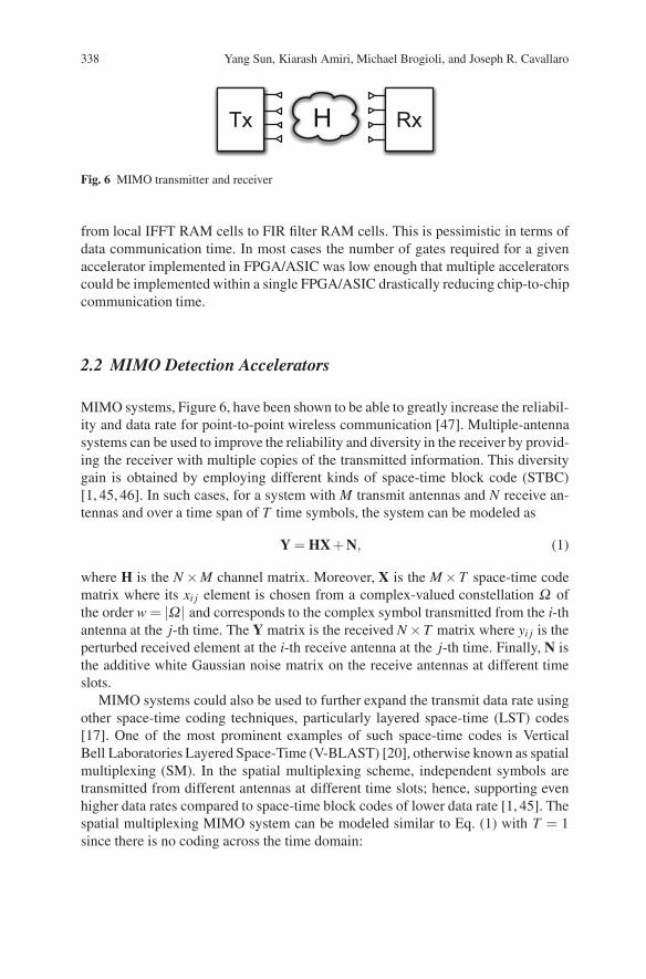
MIMO systems, Figure 6, have been shown to be able to greatly increase the reliabil-ity and data rate for point-to-point wireless communication [47]. Multiple-antennasystems can be used to improve the reliability and diversity in the receiver by provid-ing the receiver with multiple copies of the transmitted information. This diversitygain is obtained by employing different kinds of space-time block code (STBC)[1, 45, 46]. In such cases, for a system with M transmit antennas and N receive an-tennas and over a time span of T time symbols, the system can be modeled as
Y = HX+N, (1)
where H is the N×M channel matrix. Moreover, X is the M×T space-time codematrix where its xi j element is chosen from a complex-valued constellation ofthe order w = | | and corresponds to the complex symbol transmitted from the i-thantenna at the j-th time. The Y matrix is the received N×T matrix where yi j is theperturbed received element at the i-th receive antenna at the j-th time. Finally, N isthe additive white Gaussian noise matrix on the receive antennas at different timeslots.
MIMO systems could also be used to further expand the transmit data rate usingother space-time coding techniques, particularly layered space-time (LST) codes[17]. One of the most prominent examples of such space-time codes is VerticalBell Laboratories Layered Space-Time (V-BLAST) [20], otherwise known as spatialmultiplexing (SM). In the spatial multiplexing scheme, independent symbols aretransmitted from different antennas at different time slots; hence, supporting evenhigher data rates compared to space-time block codes of lower data rate [1, 45]. Thespatial multiplexing MIMO system can be modeled similar to Eq. (1) with T = 1since there is no coding across the time domain:
Application-Specific Accelerators for Communications 339
y = Hx+n, (2)
where H is the N×M channel matrix, x is the M-element column vector where itsxi-th element corresponds to the complex symbol transmitted from the i-th antenna,and y is the received N-th element column vector where yi is the perturbed receivedelement at the i-th receive antenna. The additive white Gaussian noise vector on thereceive antennas is denoted by n.
While spatial multiplexing can support very high data rates, the complexity of themaximum-likelihood detector in the receiver increases exponentially with the num-ber of transmit antennas. Thus, unlike the case in Eq. (1), the maximum-likelihooddetector for Eq. (2) requires a complex architecture and can be very costly. In orderto address this challenge, a range of detectors and solutions have been studied andimplemented. In this section, we discuss some of the main algorithmic and architec-tural features of such detectors for spatial multiplexing MIMO systems.
2.2.1 Maximum-Likelihood (ML) Detection
The Maximum Likelihood (ML) or optimal detection of MIMO signals is known tobe an NP-complete problem. The maximum-likelihood (ML) detector for Eq. (2) isfound by minimizing the
∣∣∣∣y−Hx∣∣∣∣2
2 (3)
norm over all the possible choices of x ∈ M . This brute-force search can be avery complicated task, and as already discussed, incurs an exponential complexityin the number of antennas, in fact for M transmit antennas and modulation orderof w = | |, the number of possible x vectors is wM . Thus, unless for small dimen-sion problems, it would be infeasible to implement it within a reasonable area-timeconstraint [10, 19].
2.2.2 Sphere Detection
Sphere detection can be used to achieve ML (or close-to-ML) with reduced com-plexity [15, 23] compared to ML. In fact, while the norm minimization of Eq. (3) isexponential complexity, it has been shown that using the sphere detection method,the ML solution can be obtained with much lower complexity [15].
In order to avoid the significant overhead of the ML detection, the distance normcan be simplified [13] as follows:
D(s) = ‖ y−Hs ‖2
= ‖QHy−Rs ‖2=1
i=M|yi′ −
M
j=i
Ri, js j|2, (4)
340 Yang Sun, Kiarash Amiri, Michael Brogioli, and Joseph R. Cavallaro
. . .
. . . . . ..
. . .
.. ...
. . .
...
. . .
i=M
i=M-1
i=1
1
2
w
1 w 1 2 w
2
1 2 w 1 2 w 1 2 w
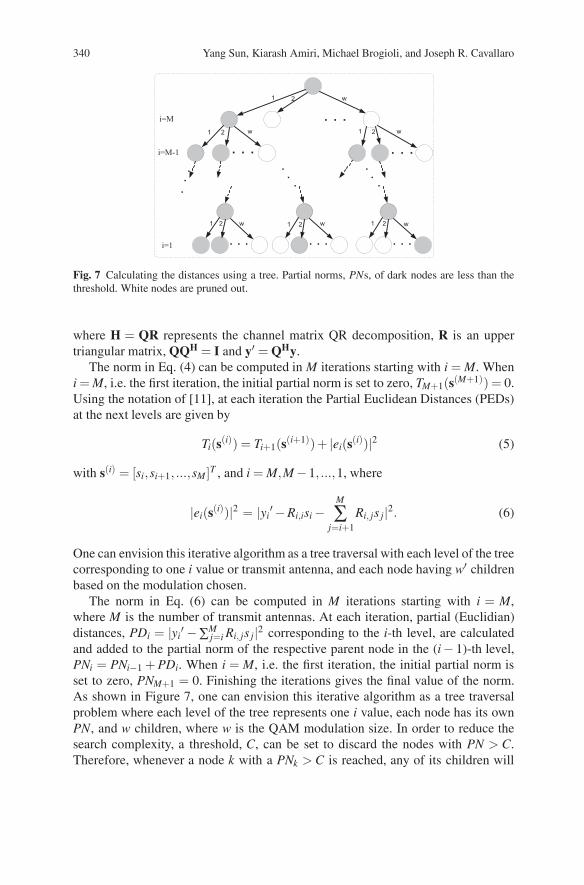
Fig. 7 Calculating the distances using a tree. Partial norms, PNs, of dark nodes are less than thethreshold. White nodes are pruned out.
where H = QR represents the channel matrix QR decomposition, R is an uppertriangular matrix, QQH = I and y′ = QHy.
The norm in Eq. (4) can be computed in M iterations starting with i = M. Wheni = M, i.e. the first iteration, the initial partial norm is set to zero, TM+1(s(M+1)) = 0.Using the notation of [11], at each iteration the Partial Euclidean Distances (PEDs)at the next levels are given by
Ti(s(i)) = Ti+1(s(i+1))+ |ei(s(i))|2 (5)
with s(i) = [si,si+1, ...,sM]T , and i = M,M−1, ...,1, where
|ei(s(i))|2 = |yi′ −Ri,isi−
M
j=i+1
Ri, js j|2. (6)
One can envision this iterative algorithm as a tree traversal with each level of the treecorresponding to one i value or transmit antenna, and each node having w′ childrenbased on the modulation chosen.
The norm in Eq. (6) can be computed in M iterations starting with i = M,where M is the number of transmit antennas. At each iteration, partial (Euclidian)distances, PDi = |yi
′ −Mj=i Ri, js j|2 corresponding to the i-th level, are calculated
and added to the partial norm of the respective parent node in the (i− 1)-th level,PNi = PNi−1 + PDi. When i = M, i.e. the first iteration, the initial partial norm isset to zero, PNM+1 = 0. Finishing the iterations gives the final value of the norm.As shown in Figure 7, one can envision this iterative algorithm as a tree traversalproblem where each level of the tree represents one i value, each node has its ownPN, and w children, where w is the QAM modulation size. In order to reduce thesearch complexity, a threshold, C, can be set to discard the nodes with PN > C.Therefore, whenever a node k with a PNk > C is reached, any of its children will
Application-Specific Accelerators for Communications 341
have PN ≥ PNk > C. Hence, not only the k-th node, but also its children, and allnodes lying beneath the children in the tree, can be pruned out.
There are different approaches to search the entire tree, mainly classified asdepth-first search (DFS) approach and K-best approach, where the latter is based onbreadth-first search (BFS) strategy. In DFS, the tree is traversed vertically [2, 11];while in BFS [22, 52], the nodes are visited horizontally, i.e. level by level.
In the DFS approach, starting from the top level, one node is selected, the PNs ofits children are calculated, and among those new computed PNs, one of them, e.g.the one with the least PN, is chosen, and that becomes the parent node for the nextiteration. The PNs of its children are calculated, and the same procedure continuesuntil a leaf is reached. At this point, the value of the global threshold is updated withthe PN of the recently visited leaf. Then, the search continues with another node ata higher level, and the search controller traverses the tree down to another leaf. Ifa node is reached with a PN larger than the radius, i.e. the global threshold, thenthat node, along with all nodes lying beneath that, are pruned out, and the searchcontinues with another node.
The tree traversal can be performed in a breadth-first manner. At each level, onlythe best K nodes, i.e. the K nodes with the smallest Ti, are chosen for expansion. Thistype of detector is generally known as the K-best detector. Note that such a detectorrequires sorting a list of size K×w′ to find the best K candidates. For instance, for a16-QAM system with K = 10, this requires sorting a list of size K×w′= 10×4 = 40at most of the tree levels.
2.2.3 Computational Complexity of Sphere Detection
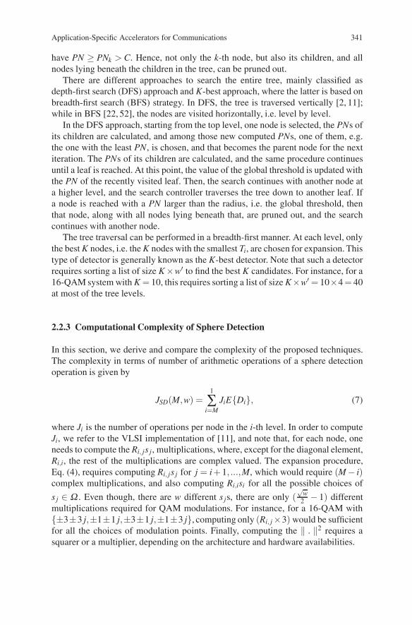
In this section, we derive and compare the complexity of the proposed techniques.The complexity in terms of number of arithmetic operations of a sphere detectionoperation is given by
JSD(M,w) =1
i=M
JiE{Di}, (7)
where Ji is the number of operations per node in the i-th level. In order to computeJi, we refer to the VLSI implementation of [11], and note that, for each node, oneneeds to compute the Ri, js j, multiplications, where, except for the diagonal element,Ri,i, the rest of the multiplications are complex valued. The expansion procedure,Eq. (4), requires computing Ri, js j for j = i+ 1, ...,M, which would require (M− i)complex multiplications, and also computing Ri,isi for all the possible choices of
s j ∈ . Even though, there are w different s js, there are only (√
w2 − 1) different
multiplications required for QAM modulations. For instance, for a 16-QAM with{±3±3 j,±1±1 j,±3±1 j,±1±3 j}, computing only (Ri, j×3) would be sufficientfor all the choices of modulation points. Finally, computing the ‖ . ‖2 requires asquarer or a multiplier, depending on the architecture and hardware availabilities.
342 Yang Sun, Kiarash Amiri, Michael Brogioli, and Joseph R. Cavallaro
Fig. 8 Number of addition and multiplications operations for 16-QAM with different number ofantennas, M.
In order to compute the number of adders for each norm expansion in (4), wenote that there are (M− i) complex valued adders required for yi
′ −Mj=i+1 Ri, js j,
and w more complex adders to add the newly computed Ri,isi values. Once the w dif-
ferent norms, |yi′ −M
j=i Ri, js j∣∣2, are computed, they need to be added to the partial
distance coming from the higher level, which requires w more addition procedures.Finally, unless the search is happening at the end of the tree, the norms need to besorted, which assuming a simple sorter, requires w(w+ 1)/2 compare-select opera-tions.
Therefore, keeping in mind that each complex multiplier corresponds to fourreal-valued multipliers and two real-valued adders, and that every complex addercorresponds to two real-valued adders, Ji is calculated by
Ji(M,w) = Jmult + Jadd(M,w)
Jmult(M,w) = ((√
w2−1)+ 4(M− i)+ 1)
Jadd(M,w) = (2(M− i)+ 2w+ w)+ (w(w+ 1)/2) · sign(i−1),
where sign(i−1) is used to ensure sorting is counted only when the search has notreached the end of the tree, and is equal to:
sign(t) ={
1 t ≥ 10 otherwise
. (8)
Moreover, we use , and to represent the hardware-oriented costs for oneadder, one compare-select unit and one multiplication operation, respectively.
Figure 8 shows the number of addition and multiplication operations needed fora 16-QAM system with different number of antennas.
Application-Specific Accelerators for Communications 343
Pre-Processing Unit(PPU)
Tree TraversalUnit
(TTU)
Computation Unit(CMPU)
Node Ordering Unit(NOU)
SphereDetector
Channel Matrix Received Vector
Detected Vector
PD Unit #1
PD Unit #2
...PD Unit
#w
Computation Unit (CMPU )
Previous PD PD_1
PD_2
PD_w
..
.
Fig. 9 Sphere Detector architecture with multiple PED function units.
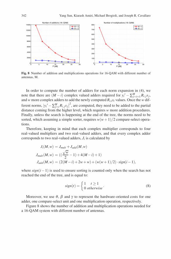
2.2.4 Depth-First Sphere Detector Architecture
The depth-first sphere detection algorithm [11, 15, 19, 23] traverses the tree in adepth-first manner: the detector visits the children of each node before visiting itssiblings. A constraint, referred to as radius, is often set on the PED for each level ofthe tree. A generic depth-first sphere detector architecture is shown in Figure 9. ThePre-Processing Unit (PPU) is used to compute the QR decomposition of the channelmatrix as well as calculate QHy. The Tree Traversal Unit (TTU) is the controllingunit which decides in which direction and with which node to continue. Computa-tion Unit (CMPU) computes the partial distances, based on (4), for w different s j.Each PD unit computes |yi
′ −Mj=i Ri, js j|2 for each of the w children of a node. Fi-
nally, the Node Ordering Unit (NOU) is for finding the minimum and saving otherlegitimate candidates, i.e. those inside Ri, in the memory.
As an example to show the algorithm complexity, an FPGA implementation syn-thesis result for a 50 Mbps 4×4 16-QAM depth-first sphere detector is summarizedin Table 2 [2].
Table 2 FPGA Resource Utilization for Sphere Detector
Device Xilinx Virtex-4 xc4vfx100-12ff1517Number of Slices 4065/42176 (9%)Number of FFs 3344/84352 (3%)
Number of Look-Up Tables 6457/84352 (7%)Number of RAMB16 3/376 (1%)Number of DSP48s 32/160 (20%)
Max. Freq. 125.7 MHz
344 Yang Sun, Kiarash Amiri, Michael Brogioli, and Joseph R. Cavallaro
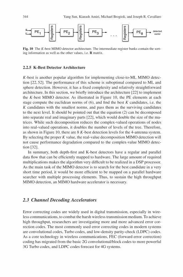
Fig. 10 The K-best MIMO detector architecture. The intermediate register banks contain the sort-ing information as well as the other values, i.e. R matrix.
2.2.5 K-Best Detector Architecture
K-best is another popular algorithm for implementing close-to-ML MIMO detec-tion [22, 52]. The performance of this scheme is suboptimal compared to ML andsphere detection. However, it has a fixed complexity and relatively straightforwardarchitecture. In this section, we briefly introduce the architecture [22] to implementthe K-best MIMO detector. As illustrated in Figure 10, the PE elements at eachstage compute the euclidean norms of (6), and find the best K candidates, i.e. theK candidates with the smallest norms, and pass them as the surviving candidatesto the next level. It should be pointed out that the equation (2) can be decomposedinto separate real and imaginary parts [22], which would double the size of the ma-trices. While such decomposition reduces the complex-valued operations of nodesinto real-valued operations, it doubles the number of levels of the tree. Therefore,as shown in Figure 10, there are 8 K-best detection levels for the 4-antenna system.By selecting the proper K value, the real-value decomposition MIMO detection willnot cause performance degradation compared to the complex-value MIMO detec-tion [32].
In summary, both depth-first and K-best detectors have a regular and paralleldata flow that can be efficiently mapped to hardware. The large amount of requiredmultiplications makes the algorithm very difficult to be realized in a DSP processor.As the main task of the MIMO detector is to search for the best candidate in a veryshort time period, it would be more efficient to be mapped on a parallel hardwaresearcher with multiple processing elements. Thus, to sustain the high throughputMIMO detection, an MIMO hardware accelerator is necessary.
2.3 Channel Decoding Accelerators
Error correcting codes are widely used in digital transmission, especially in wire-less communications, to combat the harsh wireless transmission medium. To achievehigh throughput, researchers are investigating more and more advanced error cor-rection codes. The most commonly used error correcting codes in modern systemsare convolutional codes, Turbo codes, and low-density parity-check (LDPC) codes.As a core technology in wireless communications, FEC (forward error correction)coding has migrated from the basic 2G convolutional/block codes to more powerful3G Turbo codes, and LDPC codes forecast for 4G systems.
Application-Specific Accelerators for Communications 345
As codes become more complicated, the implementation complexity, especiallythe decoder complexity, increases dramatically which largely exceeds the capabilityof the general purpose DSP processor. Even the most capable DSPs today wouldneed some types of acceleration coprocessor to offload the computation-intensiveerror correcting tasks. Moreover, it would be much more efficient to implementthese decoding algorithms on dedicated hardware because typical error correctionalgorithms use special arithmetic and therefore are more suitable for ASICs or FP-GAs. Bitwise operations, linear feedback shift registers, and complex look-up tablescan be very efficiently realized with ASICs/FPGAs.
In this section, we will present some important error correction algorithms andtheir efficient hardware architectures. We will cover major error correction codesused in the current and next generation communication standards, such as 3GPPLTE, IEEE 802.11n Wireless LAN, IEEE 802.16e WiMax, and etc.
2.3.1 Viterbi Decoder Accelerator Architecture
In telecommunications, convolutional codes are among the most popular error cor-rection codes that are used to improve the performance of wireless links. For exam-ple, convolutional codes are used in the data channel of the second generation (2G)mobile phone system (eg. GSM) and IEEE 802.11a/n wireless local area network(WLAN). Due to their good performance and efficient hardware architectures, con-volutional codes continue to be used by the 3G/4G wireless systems for their controlchannels, such as 3GPP LTE and IEEE 802.16e WiMax.
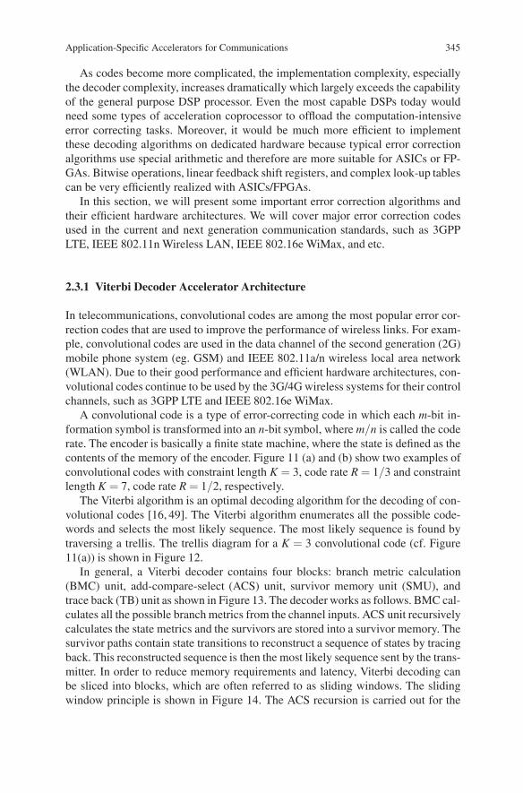
A convolutional code is a type of error-correcting code in which each m-bit in-formation symbol is transformed into an n-bit symbol, where m/n is called the coderate. The encoder is basically a finite state machine, where the state is defined as thecontents of the memory of the encoder. Figure 11 (a) and (b) show two examples ofconvolutional codes with constraint length K = 3, code rate R = 1/3 and constraintlength K = 7, code rate R = 1/2, respectively.
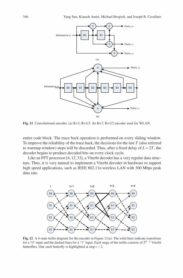
The Viterbi algorithm is an optimal decoding algorithm for the decoding of con-volutional codes [16, 49]. The Viterbi algorithm enumerates all the possible code-words and selects the most likely sequence. The most likely sequence is found bytraversing a trellis. The trellis diagram for a K = 3 convolutional code (cf. Figure11(a)) is shown in Figure 12.
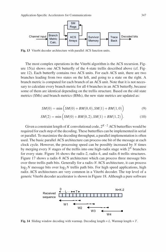
In general, a Viterbi decoder contains four blocks: branch metric calculation(BMC) unit, add-compare-select (ACS) unit, survivor memory unit (SMU), andtrace back (TB) unit as shown in Figure 13. The decoder works as follows. BMC cal-culates all the possible branch metrics from the channel inputs. ACS unit recursivelycalculates the state metrics and the survivors are stored into a survivor memory. Thesurvivor paths contain state transitions to reconstruct a sequence of states by tracingback. This reconstructed sequence is then the most likely sequence sent by the trans-mitter. In order to reduce memory requirements and latency, Viterbi decoding canbe sliced into blocks, which are often referred to as sliding windows. The slidingwindow principle is shown in Figure 14. The ACS recursion is carried out for the
346 Yang Sun, Kiarash Amiri, Michael Brogioli, and Joseph R. Cavallaro
S0 S1
+ +
+
Information u
Parity c0
Parity c1
(a)
S0 S1Information u
Parity c0
Parity c1
(b)
+
S2 S3 S4 S5
+
+ Parity c2
Fig. 11 Convolutional encoder. (a) K=3, R=1/3. (b) K=7, R=1/2 encoder used for WLAN.
entire code block. The trace back operation is performed on every sliding window.To improve the reliability of the trace back, the decisions for the last T (also referredto warmup window) steps will be discarded. Thus, after a fixed delay of L+2T , thedecoder begins to produce decoded bits on every clock cycle.
Like an FFT processor [4, 12, 33], a Viterbi decoder has a very regular data struc-ture. Thus, it is very natural to implement a Viterbi decoder in hardware to supporthigh speed applications, such as IEEE 802.11n wireless LAN with 300 Mbps peakdata rate.
S0
S1
S2
S3
S0
S1
S2
S3
S0
S1
S2
S3
S0
S1
S2
S3
S0
S1
S2
S3
t t+1 t+2 t+3 t+4
Fig. 12 A 4-state trellis diagram for the encoder in Figure 11(a). The solid lines indicate transitionsfor a “0" input and the dashed lines for a “1" input. Each stage of the trellis consists of 2K−2 Viterbibutterflies. One such butterfly is highlighted at step t +2.
Application-Specific Accelerators for Communications 347
BranchMetricCalc.
ACSArrays
SMRegs
SurvivorMemory
Channel input Trace Back
Decoded bits
Fig. 13 Viterbi decoder architecture with parallel ACS function units.
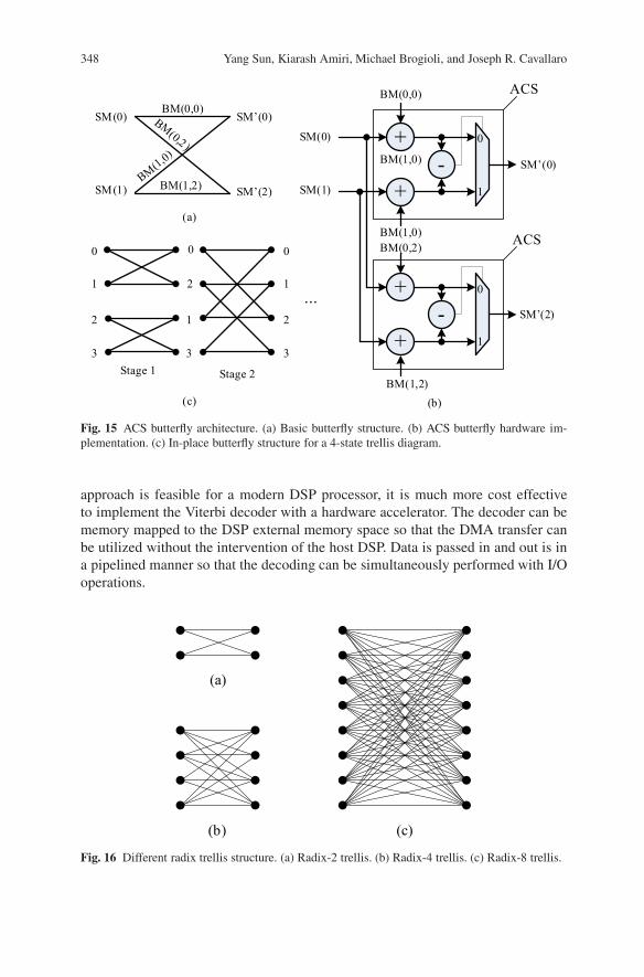
The most complex operations in the Viterbi algorithm is the ACS recursion. Fig-ure 15(a) shows one ACS butterfly of the 4-state trellis described above (cf. Fig-ure 12). Each butterfly contains two ACS units. For each ACS unit, there are twobranches leading from two states on the left, and going to a state on the right. Abranch metric is computed for each branch of an ACS unit. Note that it is not neces-sary to calculate every branch metric for all 4 branches in an ACS butterfly, becausesome of them are identical depending on the trellis structure. Based on the old statemetrics (SMs) and branch metrics (BMs), the new state metrics are updated as:
SM(0) = min(
SM(0)+ BM(0,0),SM(1)+ BM(1,0))
(9)
SM(2) = min(
SM(0)+ BM(0,2),SM(1)+ BM(1,2)). (10)
Given a constraint length of K convolutional code, 2K−2 ACS butterflies would berequired for each step of the decoding. These butterflies can be implemented in serialor parallel. To maximize the decoding throughput, a parallel implementation is oftenused. The basic parallel ACS architecture can process one bit of the message at eachclock cycle. However, the processing speed can be possibly increased by N timesby merging every N stages of the trellis into one high-radix stage with 2N branchesfor every state. Figure 16 shows the radix-2, radix-4, and radix-8 trellis structures.Figure 17 shows a radix-8 ACS architecture which can process three message bitsover three trellis path bits. Generally for a radix-N ACS architecture, it can processlog2 N message bits over log2 N trellis path bits. For high speed applications, highradix ACS architectures are very common in a Viterbi decoder. The top level of ageneric Viterbi decoder accelerator is shown in Figure 18. Although a pure software
0 N+K-2L T
W1W2
W3W4
Received sequence
Fig. 14 Sliding window decoding with warmup. Decoding length = L. Warmup length = T .
348 Yang Sun, Kiarash Amiri, Michael Brogioli, and Joseph R. Cavallaro
+
+-
SM(0)
SM(1)
SM’(0)
BM(0,0)
BM(1,0)
BM(0,0)SM(0)
SM(1)
SM’(0)
SM’(2)BM(1,2)BM(1,0)
BM(0,2)
(a)
(b)
0
1
0
1
2
3
0
2
1
3
0
1
2
3
(c)
Stage 1 Stage 2
...
BM(1,0)
ACS
BM(0,2)
BM(1,2)
SM’(2)
+
+-
0
1
ACS
Fig. 15 ACS butterfly architecture. (a) Basic butterfly structure. (b) ACS butterfly hardware im-plementation. (c) In-place butterfly structure for a 4-state trellis diagram.
approach is feasible for a modern DSP processor, it is much more cost effectiveto implement the Viterbi decoder with a hardware accelerator. The decoder can bememory mapped to the DSP external memory space so that the DMA transfer canbe utilized without the intervention of the host DSP. Data is passed in and out is ina pipelined manner so that the decoding can be simultaneously performed with I/Ooperations.
(a)
(b) (c)
Fig. 16 Different radix trellis structure. (a) Radix-2 trellis. (b) Radix-4 trellis. (c) Radix-8 trellis.
Application-Specific Accelerators for Communications 349
ACS Switch ACS Switch ACS
Fig. 17 Radix-8 ACS architecture.
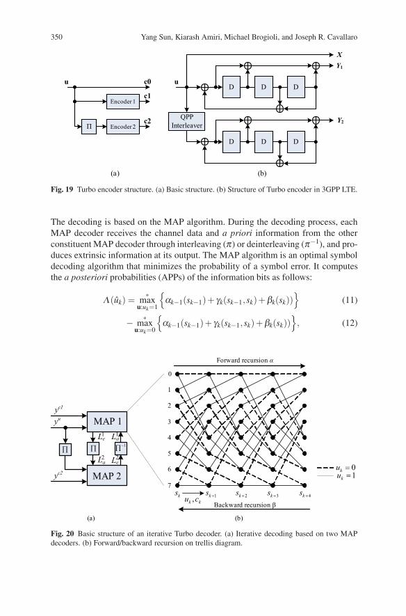
2.3.2 Turbo Decoder Accelerator Architecture
Turbo codes are a class of high-performance capacity-approaching error-correctingcodes [5]. As a break-through in coding theory, Turbo codes are widely used in many3G/4G wireless standards such as CDMA2000, WCDMA/UMTS, 3GPP LTE, andIEEE 802.16e WiMax. However, the inherently large decoding latency and complexiterative decoding algorithm have made it rarely being implemented in a generalpurpose DSP. For example, Texas Instruments’ latest multi-core DSP processor TIC6474 employs a Turbo decoder accelerator to support 2 Mbps CDMA Turbo codesfor the base station [27]. The decoding throughput requirement for 3GPP LTE Turbocodes is to be more than 80 Mbps in the uplink and 320 Mbps in the downlink. Be-cause the Turbo codes used in many standards are very similar, e.g. the encodingpolynomials are same for WCDMA/UMTS/LTE, the Turbo decoder is often accel-erated by reconfigurable hardware.
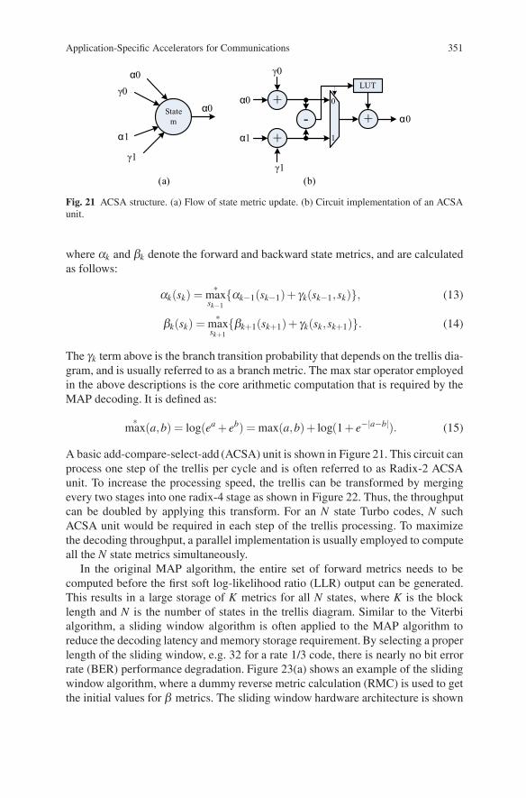
A classic Turbo encoder structure is depicted in Figure 19. The basic encoderconsists of two systematic convolutional encoders and an interleaver. The informa-tion sequence u is encoded into three streams: systematic, parity 1, and parity 2.Here the interleaver is used to permute the information sequence into a second dif-ferent sequence for encoder 2. The performance of a Turbo code depends criticallyon the interleaver structure [36].
The BCJR algorithm [3], also called forward-backward algorithm or Maximuma posteriori (MAP) algorithm, is the main component in the Turbo decoding pro-cess. The basic structure of Turbo decoding is functionally illustrated in Figure 20.
BranchMetricCalc.
RegisterArrays
Survivors & Trace Back
DSP CoreDMA
EMIF
DSP Processor
DS
P IF
Viterbi Decoder Accelerator
Radix-NACS
Arrays
Fig. 18 A generic Viterbi decoder accelerator architecture. Data movement between DSP proces-sor and accelerator is via DMA. Fully-parallel ACS function units are used to support high speeddecoding.
350 Yang Sun, Kiarash Amiri, Michael Brogioli, and Joseph R. Cavallaro
QPPInterleaver
D D D
D D D
u
XY1
Y2Π Encoder 2
Encoder 1
u c0
c1
c2
(a) (b)
Fig. 19 Turbo encoder structure. (a) Basic structure. (b) Structure of Turbo encoder in 3GPP LTE.
The decoding is based on the MAP algorithm. During the decoding process, eachMAP decoder receives the channel data and a priori information from the otherconstituent MAP decoder through interleaving () or deinterleaving (−1), and pro-duces extrinsic information at its output. The MAP algorithm is an optimal symboldecoding algorithm that minimizes the probability of a symbol error. It computesthe a posteriori probabilities (APPs) of the information bits as follows:
(uk) =∗
maxu:uk=1
{k−1(sk−1)+ k(sk−1,sk)+k(sk))
}(11)
− ∗max
u:uk=0
{k−1(sk−1)+ k(sk−1,sk)+k(sk))
}, (12)
ks 1+ks
0
1
2
3
4
5
6
72+ks 3+ks 4+ks
kk cu ,
0=ku1=ku
Forward recursion α
Backward recursion β
MAP 1
MAP 2
1−∏
yuyc1
yc2
LaLe
∏∏La Le
(a) (b)
1 1
2 2
Fig. 20 Basic structure of an iterative Turbo decoder. (a) Iterative decoding based on two MAPdecoders. (b) Forward/backward recursion on trellis diagram.
Application-Specific Accelerators for Communications 351
+
+-
0
1
LUT
+State m
γ0α0
(a) (b)
α1
γ1
α0
γ0
α0
γ1
α1
α0
Fig. 21 ACSA structure. (a) Flow of state metric update. (b) Circuit implementation of an ACSAunit.
where k and k denote the forward and backward state metrics, and are calculatedas follows:
k(sk) =∗
maxsk−1{k−1(sk−1)+ k(sk−1,sk)}, (13)
k(sk) =∗
maxsk+1{k+1(sk+1)+ k(sk,sk+1)}. (14)
The k term above is the branch transition probability that depends on the trellis dia-gram, and is usually referred to as a branch metric. The max star operator employedin the above descriptions is the core arithmetic computation that is required by theMAP decoding. It is defined as:
∗max(a,b) = log(ea + eb) = max(a,b)+ log(1 + e−|a−b|). (15)
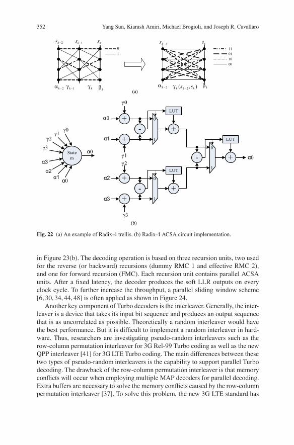
A basic add-compare-select-add (ACSA) unit is shown in Figure 21. This circuit canprocess one step of the trellis per cycle and is often referred to as Radix-2 ACSAunit. To increase the processing speed, the trellis can be transformed by mergingevery two stages into one radix-4 stage as shown in Figure 22. Thus, the throughputcan be doubled by applying this transform. For an N state Turbo codes, N suchACSA unit would be required in each step of the trellis processing. To maximizethe decoding throughput, a parallel implementation is usually employed to computeall the N state metrics simultaneously.
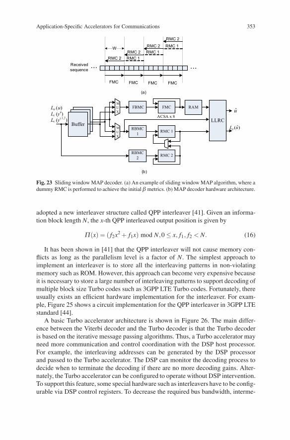
In the original MAP algorithm, the entire set of forward metrics needs to becomputed before the first soft log-likelihood ratio (LLR) output can be generated.This results in a large storage of K metrics for all N states, where K is the blocklength and N is the number of states in the trellis diagram. Similar to the Viterbialgorithm, a sliding window algorithm is often applied to the MAP algorithm toreduce the decoding latency and memory storage requirement. By selecting a properlength of the sliding window, e.g. 32 for a rate 1/3 code, there is nearly no bit errorrate (BER) performance degradation. Figure 23(a) shows an example of the slidingwindow algorithm, where a dummy reverse metric calculation (RMC) is used to getthe initial values for metrics. The sliding window hardware architecture is shown
352 Yang Sun, Kiarash Amiri, Michael Brogioli, and Joseph R. Cavallaro
+
+-
0
1
LUT
+
+
+-
0
1
LUT
+
-0
1
LUT
+State
m
11011000
kβ1−kγ kγ
2−ks 1−ks ks2−ks ks
2−kα kβ),( 2 kkk ss −γ2−kα
01
(a)
(b)
γ0
α0
γ1γ2
γ3
α1α2
α3
α0
γ0
α0
α1
γ1γ2
γ3
α2
α3
α0
Fig. 22 (a) An example of Radix-4 trellis. (b) Radix-4 ACSA circuit implementation.
in Figure 23(b). The decoding operation is based on three recursion units, two usedfor the reverse (or backward) recursions (dummy RMC 1 and effective RMC 2),and one for forward recursion (FMC). Each recursion unit contains parallel ACSAunits. After a fixed latency, the decoder produces the soft LLR outputs on everyclock cycle. To further increase the throughput, a parallel sliding window scheme[6, 30, 34, 44, 48] is often applied as shown in Figure 24.
Another key component of Turbo decoders is the interleaver. Generally, the inter-leaver is a device that takes its input bit sequence and produces an output sequencethat is as uncorrelated as possible. Theoretically a random interleaver would havethe best performance. But it is difficult to implement a random interleaver in hard-ware. Thus, researchers are investigating pseudo-random interleavers such as therow-column permutation interleaver for 3G Rel-99 Turbo coding as well as the newQPP interleaver [41] for 3G LTE Turbo coding. The main differences between thesetwo types of pseudo-random interleavers is the capability to support parallel Turbodecoding. The drawback of the row-column permutation interleaver is that memoryconflicts will occur when employing multiple MAP decoders for parallel decoding.Extra buffers are necessary to solve the memory conflicts caused by the row-columnpermutation interleaver [37]. To solve this problem, the new 3G LTE standard has
Application-Specific Accelerators for Communications 353
Buffer
FBMC
RBMC 1
FMC RAM
LLRC
uMUX
MUX
Lc (yu)Lc (yc1,2)
La (u)
)ˆ(uLe
RBMC 2
RMC 1
RMC 2
ACSA x 8
W
Received sequence
... ...
FMC FMC FMC FMC
RMC 2 RMC 1RMC 2 RMC 1
RMC 2 RMC 1
RMC 2
(a)
(b)
Fig. 23 Sliding window MAP decoder. (a) An example of sliding window MAP algorithm, where adummy RMC is performed to achieve the initial metrics. (b) MAP decoder hardware architecture.
adopted a new interleaver structure called QPP interleaver [41]. Given an informa-tion block length N, the x-th QPP interleaved output position is given by
(x) = ( f2x2 + f1x) mod N,0 ≤ x, f1, f2 < N. (16)
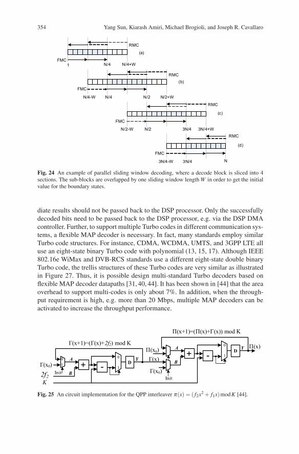
It has been shown in [41] that the QPP interleaver will not cause memory con-flicts as long as the parallelism level is a factor of N. The simplest approach toimplement an interleaver is to store all the interleaving patterns in non-violatingmemory such as ROM. However, this approach can become very expensive becauseit is necessary to store a large number of interleaving patterns to support decoding ofmultiple block size Turbo codes such as 3GPP LTE Turbo codes. Fortunately, thereusually exists an efficient hardware implementation for the interleaver. For exam-ple, Figure 25 shows a circuit implementation for the QPP interleaver in 3GPP LTEstandard [44].
A basic Turbo accelerator architecture is shown in Figure 26. The main differ-ence between the Viterbi decoder and the Turbo decoder is that the Turbo decoderis based on the iterative message passing algorithms. Thus, a Turbo accelerator mayneed more communication and control coordination with the DSP host processor.For example, the interleaving addresses can be generated by the DSP processorand passed to the Turbo accelerator. The DSP can monitor the decoding process todecide when to terminate the decoding if there are no more decoding gains. Alter-nately, the Turbo accelerator can be configured to operate without DSP intervention.To support this feature, some special hardware such as interleavers have to be config-urable via DSP control registers. To decrease the required bus bandwidth, interme-
354 Yang Sun, Kiarash Amiri, Michael Brogioli, and Joseph R. Cavallaro
FMC1 N/4
FMC
N/4 N/2
RMC
RMC
FMC
N/2 3N/4
RMC
N/4+W
N/4-W
N/2-W
FMC
3N/4 N3N/4-W
RMC
(a)
(b)
(c)
(d)
N/2+W
3N/4+W
Fig. 24 An example of parallel sliding window decoding, where a decode block is sliced into 4sections. The sub-blocks are overlapped by one sliding window length W in order to get the initialvalue for the boundary states.
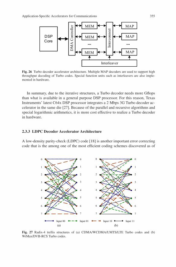
diate results should not be passed back to the DSP processor. Only the successfullydecoded bits need to be passed back to the DSP processor, e.g. via the DSP DMAcontroller. Further, to support multiple Turbo codes in different communication sys-tems, a flexible MAP decoder is necessary. In fact, many standards employ similarTurbo code structures. For instance, CDMA, WCDMA, UMTS, and 3GPP LTE alluse an eight-state binary Turbo code with polynomial (13, 15, 17). Although IEEE802.16e WiMax and DVB-RCS standards use a different eight-state double binaryTurbo code, the trellis structures of these Turbo codes are very similar as illustratedin Figure 27. Thus, it is possible design multi-standard Turbo decoders based onflexible MAP decoder datapaths [31, 40, 44]. It has been shown in [44] that the areaoverhead to support multi-codes is only about 7%. In addition, when the through-put requirement is high, e.g. more than 20 Mbps, multiple MAP decoders can beactivated to increase the throughput performance.
+
A
B
Y
K
П(x)П(x0)Г(x)
2f2
Г(x0)Г(x0)
D
П(x+1)=(П(x)+Г(x)) mod K
Г(x+1)=(Г(x)+2f2) mod K
-
+
0A
B
YD-
Init1
0
101
Init
Fig. 25 An circuit implementation for the QPP interleaver (x) = ( f2x2 + f1x)mod K [44].
Application-Specific Accelerators for Communications 355
...
Inte
rcon
nect
MEM
MAP
MAP
MEM
MEM
MAP
Interleaver
DSP Core ...
DM
A C
ontro
ller
Fig. 26 Turbo decoder accelerator architecture. Multiple MAP decoders are used to support highthroughput decoding of Turbo codes. Special function units such as interleavers are also imple-mented in hardware.
In summary, due to the iterative structures, a Turbo decoder needs more Gflopsthan what is available in a general purpose DSP processor. For this reason, TexasInstruments’ latest C64x DSP processor integrates a 2 Mbps 3G Turbo decoder ac-celerator in the same die [27]. Because of the parallel and recursive algorithms andspecial logarithmic arithmetics, it is more cost effective to realize a Turbo decoderin hardware.
2.3.3 LDPC Decoder Accelerator Architecture
A low-density parity-check (LDPC) code [18] is another important error correctingcode that is the among one of the most efficient coding schemes discovered as of
0 0
1 1
2 2
3 3
4 4
5 5
6 6
7 7
Input 00 Input 01 Input 10 Input 11
(a)
0
1
2
3
4
5
6
7
0
1
2
3
4
5
6
7
(b)
Fig. 27 Radix-4 trellis structures of (a) CDMA/WCDMA/UMTS/LTE Turbo codes and (b)WiMax/DVB-RCS Turbo codes.
356 Yang Sun, Kiarash Amiri, Michael Brogioli, and Joseph R. Cavallaro
PEV 1
PEV2
PEV3
PEV N
PEC 1 PEC 2 PEC M
...
...
SoftIn/Out
SoftIn/Out
SoftIn/Out
SoftIn/Out
Check memory + Interconnects
PEC 1 PEC 2 PEC z...
...PEV 1
PEV 2
PEV z
Variable memory + Interconnects
(a) (b)
PEVN-1
SoftIn/Out
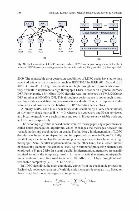
Fig. 28 Implementation of LDPC decoders, where PEC denotes processing element for checknode and PEV denotes processing element for variable node. (a) Fully-parallel. (b) Semi-parallel.
2009. The remarkable error correction capabilities of LDPC codes have led to theirrecent adoption in many standards, such as IEEE 802.11n, IEEE 802.16e, and IEEE802 10GBase-T. The huge computation and high throughput requirements make itvery difficult to implement a high throughput LDPC decoder on a general purposeDSP. For example, a 5.4 Mbps LDPC decoder was implemented on TMS320C64xxDSP running at 600 MHz [29]. This throughput performance is not enough to sup-port high data rates defined in new wireless standards. Thus, it is important to de-velop area and power efficient hardware LDPC decoding accelerators.
A binary LDPC code is a linear block code specified by a very sparse binaryM×N parity check matrix: H ·xT = 0, where x is a codeword and H can be viewedas a bipartite graph where each column and row in H represent a variable node anda check node, respectively.
The decoding algorithm is based on the iterative message passing algorithm (alsocalled belief propagation algorithm), which exchanges the messages between thevariable nodes and check nodes on graph. The hardware implementation of LDPCdecoders can be serial, semi-parallel, and fully-parallel as shown in Figure 28. Fully-parallel implementation has the maximum processing elements to achieve very highthroughput. Semi-parallel implementation, on the other hand, has a lesser numberof processing elements that can be re-used, e.g. z number of processing elements areemployed in Figure 28(b). In a semi-parallel implementation, memories are usuallyrequired to store the temporary results. In many practical systems, semi-parallelimplementations are often used to achieve 100 Mbps to 1 Gbps throughput withreasonable complexity [7, 21, 35, 42, 43, 54].
In LDPC decoding, the main complexity comes from the check node processing.Each check node receives a set of variable node messages denoted as Nm. Based onthese data, check node messages are computed as
mn = j∈Nm\n
�m j =(
j∈Nm
�m j
)�mn,
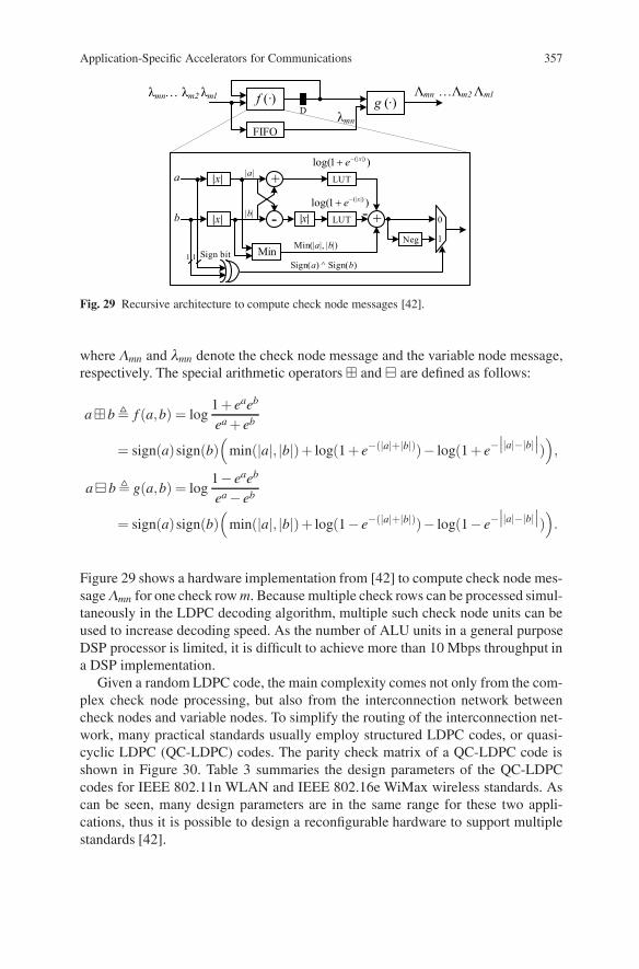
Application-Specific Accelerators for Communications 357
f (·) g (·)
FIFO
λmn… λm2 λm1
λmn
Λmn …Λm2 Λm1
+
-
MinSign bit
LUT
LUT -Neg
a
b
|a|
|b|
)1log( |)(|xe−+
Sign(a) ^ Sign(b)
Min(|a|, |b|)1 1
+
|x|
|x| |x|
D
)1log( |)(|xe−+0
1
Fig. 29 Recursive architecture to compute check node messages [42].
where mn and mn denote the check node message and the variable node message,respectively. The special arithmetic operators � and � are defined as follows:
a � b � f (a,b) = log1 + eaeb
ea + eb
= sign(a)sign(b)(
min(|a|, |b|)+ log(1 + e−(|a|+|b|))− log(1 + e−∣∣|a|−|b|∣∣)),
a � b � g(a,b) = log1− eaeb
ea− eb
= sign(a)sign(b)(
min(|a|, |b|)+ log(1− e−(|a|+|b|))− log(1− e−∣∣|a|−|b|∣∣)).
Figure 29 shows a hardware implementation from [42] to compute check node mes-sagemn for one check row m. Because multiple check rows can be processed simul-taneously in the LDPC decoding algorithm, multiple such check node units can beused to increase decoding speed. As the number of ALU units in a general purposeDSP processor is limited, it is difficult to achieve more than 10 Mbps throughput ina DSP implementation.
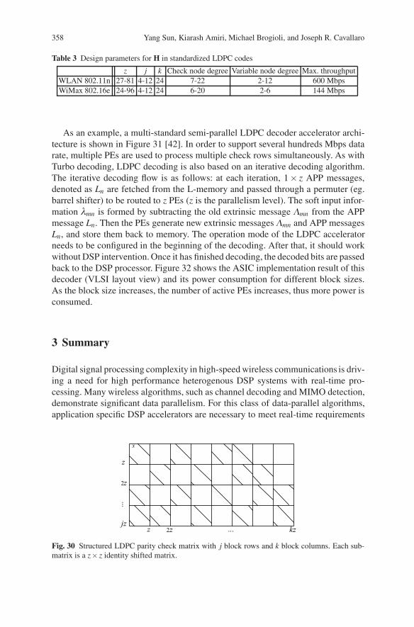
Given a random LDPC code, the main complexity comes not only from the com-plex check node processing, but also from the interconnection network betweencheck nodes and variable nodes. To simplify the routing of the interconnection net-work, many practical standards usually employ structured LDPC codes, or quasi-cyclic LDPC (QC-LDPC) codes. The parity check matrix of a QC-LDPC code isshown in Figure 30. Table 3 summaries the design parameters of the QC-LDPCcodes for IEEE 802.11n WLAN and IEEE 802.16e WiMax wireless standards. Ascan be seen, many design parameters are in the same range for these two appli-cations, thus it is possible to design a reconfigurable hardware to support multiplestandards [42].
358 Yang Sun, Kiarash Amiri, Michael Brogioli, and Joseph R. Cavallaro
Table 3 Design parameters for H in standardized LDPC codes
z j k Check node degree Variable node degree Max. throughputWLAN 802.11n 27-81 4-12 24 7-22 2-12 600 MbpsWiMax 802.16e 24-96 4-12 24 6-20 2-6 144 Mbps
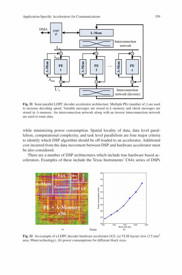
As an example, a multi-standard semi-parallel LDPC decoder accelerator archi-tecture is shown in Figure 31 [42]. In order to support several hundreds Mbps datarate, multiple PEs are used to process multiple check rows simultaneously. As withTurbo decoding, LDPC decoding is also based on an iterative decoding algorithm.The iterative decoding flow is as follows: at each iteration, 1× z APP messages,denoted as Ln are fetched from the L-memory and passed through a permuter (eg.barrel shifter) to be routed to z PEs (z is the parallelism level). The soft input infor-mation mn is formed by subtracting the old extrinsic message mn from the APPmessage Ln. Then the PEs generate new extrinsic messages mn and APP messagesLn, and store them back to memory. The operation mode of the LDPC acceleratorneeds to be configured in the beginning of the decoding. After that, it should workwithout DSP intervention. Once it has finished decoding, the decoded bits are passedback to the DSP processor. Figure 32 shows the ASIC implementation result of thisdecoder (VLSI layout view) and its power consumption for different block sizes.As the block size increases, the number of active PEs increases, thus more power isconsumed.
3 Summary
Digital signal processing complexity in high-speed wireless communications is driv-ing a need for high performance heterogenous DSP systems with real-time pro-cessing. Many wireless algorithms, such as channel decoding and MIMO detection,demonstrate significant data parallelism. For this class of data-parallel algorithms,application specific DSP accelerators are necessary to meet real-time requirements
z 2z ... kz
z
2z
jz
x
...
Fig. 30 Structured LDPC parity check matrix with j block rows and k block columns. Each sub-matrix is a z× z identity shifted matrix.
Application-Specific Accelerators for Communications 359
PE1Λ
-Mem
L-Mem
Interconnection network
. . .
+-λmn
L’n
Λmn
Ln
+
PE2Λ
-Mem
+-
+
PEzΛ
-Mem
+-
+
DSP IF
DMA
Interconnection network (Inverse)
Fig. 31 Semi-parallel LDPC decoder accelerator architecture. Multiple PEs (number of z) are usedto increase decoding speed. Variable messages are stored in L-memory and check messages arestored in -memory. An interconnection network along with an inverse interconnection networkare used to route data.
while minimizing power consumption. Spatial locality of data, data level paral-lelism, computational complexity, and task level parallelism are four major criteriato identify which DSP algorithm should be off-loaded to an accelerator. Additionalcost incurred from the data movement between DSP and hardware accelerator mustbe also considered.
There are a number of DSP architectures which include true hardware based ac-celerators. Examples of these include the Texas Instruments’ C64x series of DSPs
PE + Λ-Memoryx96
L-MemPermuter DSP I/F
Ctrl MO
R
Misc Logic
(a) 5mm
500 1000 1500 2000 2500250
275
300
325
350
375
400
425
450
Block size (bit)
)W
m( noitpmusnoc re
woP
(b)
Fig. 32 An example of a LDPC decoder hardware accelerator [42]. (a) VLSI layout view (3.5 mm2
area, 90nm technology). (b) power consumptions for different block sizes.
360 Yang Sun, Kiarash Amiri, Michael Brogioli, and Joseph R. Cavallaro
which include a 2 Mbps Turbo decoding accelerator [27], and Freescale Semicon-ductor’s six core broadband wireless access DSP MSC8156 which includes a pro-grammable 200 Mbps Turbo decoding accelerator (6 iterations), a 115 Mbps Viterbidecoding accelerator (K = 9), an FFT/IFFT accelerator for sizes 128, 256, 512, 1024or 2048 points at up to 350 million samples/s, and a DFT/IDFT for sizes up to 1536points at up to 175 million samples/s [38].
Relying on a single DSP processor for all signal processing tasks would be aclean solution. As a practical matter, however, multiple DSP processors are nec-essary for implementing a next generation wireless handset or base station. Thismeans greater system cost, more board space, and more power consumption. Inte-grating hardware communication accelerators, such as MIMO detectors and chan-nel decoders, into the DSP processor silicon can create an efficient System on Chip.This offers many advantage: the dedicated accelerators relieve the DSP processorof the parallel computation-intensive signal processing burden, freeing DSP pro-cessing capacity for other system control functions that more greatly benefit fromprogrammability.
References
1. Alamouti, S.M.: A simple transmit diversity technique for wireless communications. IEEEJournal on Selected Areas in Communications 16(8), 1451–1458 (1998)
2. Amiri, K., Cavallaro, J.R.: FPGA implementation of dynamic threshold sphere detection forMIMO systems. IEEE Asilomar Conference on Signals, Systems and Computers pp. 94–98(2006)
3. Bahl, L., Cocke, J., Jelinek, F., Raviv, J.: Optimal decoding of linear codes for minimizingsymbol error rate. IEEE Transactions on Information Theory IT-20, 284–287 (1974)
4. Bass, B.: A low-power, high-performance, 1024-point FFT processor. In: IEEE InternationalSolid-State Circuit Conference (ISSCC) (1999)
5. Berrou, C., Glavieux, A., Thitimajshima, P.: Near Shannon limit error-correcting coding anddecoding: Turbo-codes. In: IEEE International Conference on Communications, pp. 1064–1070 (1993)
6. Bougard, B., Giulietti, A., Derudder, V., Weijers, J.W., Dupont, S., Hollevoet, L., Catthoor, F.,Van der Perre, L., De Man, H., Lauwereins, R.: A scalable 8.7-nJ/bit 75.6-Mb/s parallel con-catenated convolutional (turbo-) codec. In: IEEE International Solid-State Circuit Conference(ISSCC) (2003)
7. Brack, T., Alles, M., Lehnigk-Emden, T., Kienle, F., Wehn, N., Lapos, Insalata, N., Rossi, F.,Rovini, M., Fanucci, L.: Low complexity LDPC code decoders for next generation standards.In: Design, Automation, and Test in Europe (DATE), pp. 1–6 (2007)
8. Brogioli, M.: Reconfigurable heterogeneous DSP/FPGA based embedded architectures fornumerically intensive embedded computingworkloads. Ph.D. thesis, Rice University, Hous-ton, Texas, USA (2007)
9. Brogioli, M., Radosavljevic, P., Cavallaro, J.: A general hardware/software codesign method-ology for embedded signal processing and multimedia workloads. In: IEEE 40th AsilomarConference on Signals, Systems, and Computers, pp. 1486–1490 (2006)
10. Burg, A.: VLSI circuits for MIMO communication systems. Ph.D. thesis, Swiss FederalInstitute of Technology, Zurich, Switzerland (2006)
11. Burg, A., Borgmann, M., Wenk, M., Zellweger, M., Fichtner, W., Bolcskei, H.: VLSI im-plementation of MIMO detection using the sphere decoding algorithm. IEEE Journal ofSolid-State Circuits 40(7), 1566–1577 (2005)
Application-Specific Accelerators for Communications 361
12. Cooley, J.W., Tukey, J.W.: An algorithm for the machine calculation of complex Fourier se-ries. Mathematics of Computation 19, 297–301 (1965)
13. Damen, M.O., Gamal, H.E., Caire, G.: On maximum likelihood detection and the search forthe closest lattice point. IEEE Transactions on Information Theory 49(10), 2389–2402 (2003)
14. Devices, A.: The SHARC Processor Family. http://www.analog.com/en/embedded-processing-dsp/sharc/processors/index.html (2009)
15. Fincke, U., Pohst, M.: Improved methods for calculating vectors of short length in a lattice,including a complexity analysis. Mathematics of Computation 44(170), 463–471 (1985)
16. Forney, G.D.: The Viterbi algorithm. Proceedings of the IEEE 61(3), 268–278 (1973)17. Foschini, G.: Layered space-time architecture for wireless communication in a fading envi-
ronment when using multiple antennas. Bell Labs. Tech. Journal 2, 41–59 (1996)18. Gallager, R.: Low-density parity-check codes. IEEE Transactions on Information Theory 8,
21–28 (1962)19. Garrett, D., Davis, L., ten Brink, S., Hochwald, B., Knagge, G.: Silicon complexity for max-
imum likelihood MIMO detection using spherical decoding. IEEE Journal of Solid-StateCircuits 39(9), 1544–1552 (2004)
20. Golden, G., Foschini, G.J., Valenzuela, R.A., Wolniansky, P.W.: Detection algorithms andinitial laboratory results using V-BLAST space-time communication architecture. ElectronicsLetters 35, 14–15 (1999)
21. Gunnam, K., Choi, G.S., Yeary, M.B., Atiquzzaman, M.: VLSI architectures for layered de-coding for irregular LDPC codes of WiMax. In: IEEE International Conference on Commu-nications, pp. 4542–4547 (2007)
22. Guo, Z., Nilsson, P.: Algorithm and implementation of the K-best sphere decoding for MIMOdetection. IEEE Journal on Selected Areas in Communications 24(3), 491–503 (2006)
23. Hassibi, B., Vikalo, H.: On the sphere-decoding algorithm I. Expected complexity. IEEETransactions on Signal Processing 53(8), 2806–2818 (2005)
24. Hunter, H.C., Moreno, J.H.: A new look at exploiting data parallelism in embedded systems.In: Proceedings of the International Conference on Compilers, Architectures and Synthesisfor Embedded Systems, pp. 159–169 (2003)
25. Tensilica Inc.: http://www.tensilica.com (2009)26. Texas Instruments: TMS320C55x DSP CPU Programmer’s Reference Supplement.
http://focus.ti.com/lit/ug/spru652g/spru652g.pdf (2005)27. Texas Instruments: TMS320C6474 high performance multicore processor datasheet.
http://focus.ti.com/docs/prod/folders/print/tms320c6474.html (2008)28. Instruments, T.: TMS320C6000 CPU and Instruction Set Reference Guide.
http://dspvillage.ti.com (2001)29. Lechner, G., Sayir, J., Rupp, M.: Efficient DSP implementation of an LDPC decoder. In: IEEE
International Conference on Acoustics, Speech, and Signal Processing (ICASSP), vol. 4, pp.665–668 (2004)
30. Lee, S.J., Shanbhag, N.R., Singer, A.C.: Area-efficient high-throughput MAP decoder archi-tectures. IEEE Transactions on VLSI Systems 13, 921–933 (2005)
31. Martina, M., Nicola, M., Masera, G.: A flexible UMTS-WiMax turbo decoder architecture.IEEE Transactions on Circuits and Systems II 55, 369–273 (2008)
32. Myllylä, M., Silvola, P., Juntti, M., Cavallaro, J.R.: Comparison of two novel list sphere detec-tor algorithms for mimo-ofdm systems. IEEE International Symposium on Personal Indoorand Mobile Radio Communications (2006)
33. Parhi, K.K.: VLSI Digital Signal Processing Systems Design and Implementation. Wiley(1999)
34. Prescher, G., Gemmeke, T., Noll, T.G.: A parametrizable low-power high-throughput turbo-decoder. In: IEEE International Conference on Acoustics, Speech, and Signal Processing(ICASSP), vol. 5, pp. 25–28 (2005)
35. Rovini, M., Gentile, G., Rossi, F., Fanucci, L.: A scalable decoder architecture for IEEE802.11n LDPC codes. In: IEEE Global Telecommunications Conference, pp. 3270–3274(2007)
362 Yang Sun, Kiarash Amiri, Michael Brogioli, and Joseph R. Cavallaro
36. Sadjadpour, H., Sloane, N., Salehi, M., Nebe, G.: Interleaver design for turbo codes. IEEEJournal on Seleteced Areas in Communications 19, 831–837 (2001)
37. Salmela, P., Gu, R., Bhattacharyya, S., Takala, J.: Efficient parallel memory organization forturbo decoders. In: Proc. European Signal Processing Conf., pp. 831–835 (2007)
38. Freescale Semiconductor: MSC8156 six core broadband wireless access DSP.www.freescale.com/starcore (2009)
39. Semiconductor, F.: Freescale Starcore Architecture. www.freescale.com/starcore (2009)40. Shin, M.C., Park, I.C.: A programmable turbo decoder for multiple 3G wireless standards.
In: IEEE Solid-State Circuits Conference, vol. 1, pp. 154–484 (2003)41. Sun, J., Takeshita, O.: Interleavers for turbo codes using permutation polynomials over integer
rings. IEEE Transactions on Information Theory 51(1) (2005)42. Sun, Y., Cavallaro, J.R.: A low-power 1-Gbps reconfigurable LDPC decoder design for mul-
tiple 4G wireless standards. In: IEEE International SOC Conference (SoCC), pp. 367–370(2008)
43. Sun, Y., Karkooti, M., Cavallaro, J.R.: VLSI decoder architecture for high throughput, vari-able block-size and multi-rate LDPC codes. In: IEEE International Symposium on Circuitsand Systems (ISCAS), pp. 2104–2107 (2007)
44. Sun, Y., Zhu, Y., Goel, M., Cavallaro, J.R.: Configurable and scalable high throughput turbodecoder architecture for multiple 4G wireless standards. In: IEEE International Conferenceon Application-Specific Systems, Architectures and Processors (ASAP), pp. 209–214 (2008)
45. Tarokh, V., Jafarkhani, H., Calderbank, A.R.: Space-time block codes from orthogonal de-signs. IEEE Transactions on Information Theory 45(5), 1456–1467 (1999)
46. Tarokh, V., Jafarkhani, H., Calderbank, A.R.: Space time block coding for wireless commu-nications: Performance results. IEEE Journal on Selected Areas in Communications 17(3),451–460 (1999)
47. Telatar, I.E.: Capacity of multiantenna Gaussian channels. European Transactions onTelecommunications 10, 585–595 (1999)
48. Thul, M.J., Gilbert, F., Vogt, T., Kreiselmaier, G., Wehn, N.: A scalable system architecturefor high-throughput turbo-decoders. Journal of VLSI Signal Processing pp. 63–77 (2005)
49. Viterbi, A.: Error bounds for convolutional coding and an asymptotically optimum decodingalgorithm. IEEE Transactions on Information Theory IT-13, 260–269 (1967)
50. Wijting, C., Ojanperä, T., Juntti, M., Kansanen, K., Prasad, R.: Groupwise serial multiuserdetectors for multirate DS-CDMA. In: IEEE Vehicular Technology Conference, vol. 1, pp.836–840 (1999)
51. Willmann, P., Kim, H., Rixner, S., Pai, V.S.: An efficient programmable 10 Gigabit Ethernetnetwork interface card. In: ACM International Symposium on High-Performance ComputerArchitecture, pp. 85–86 (2006)
52. Wong, K., Tsui, C., Cheng, R.S., Mow, W.: A VLSI architecture of a K-best lattice decodingalgorithm for MIMO channels. IEEE International Symposium on Circuits and Systems 3,273–276 (2002)
53. Ye, Z.A., Moshovos, A., Hauck, S., Banerjee, P.: CHIMAERA: A High–Performance Archi-tecture with a Tightly–Coupled Reconfigurable Functional Unit. In: Proceedings of the 27thAnnual International Symposium on Computer Architecture, pp. 225–235 (2000)
54. Zhong, H., Zhang, T.: Block-LDPC: a practical LDPC coding system design approach. IEEETransactions on Circuits and Systems I: Fundamental Theory and Applications 52(4), 766–775 (2005)