Embed Size (px)
Citation preview
SEC-Mobile-UtRAM
Application Note for
General PCB Design Guidelines
for Mobile DRAM Version 1.0, May 2009
Samsung Electronics
Copyright ⓒ 2009 Samsung Electronics Co., LTD.
Samsung Electronics Co; LTD 2
Copyright © 2009 Samsung Electronics Co, Ltd. All Rights Reserved.
Though every care has been taken to ensure the accuracy of this document, Samsung
Electronics Co, Ltd. cannot accept responsibility for any errors or omissions or for any
loss occurred to any person, whether legal or natural, from acting, or refraining from
action, as a result of the information contained herein. Information in this document is
subject to change at any time without obligation to notify any person of such changes.
Samsung Electronics Co, Ltd. may have patents or patent pending applications,
trademarks copyrights or other intellectual property rights covering subject matter in this
document. The furnishing of this document does not give the recipient or reader any
license to these patents, trademarks copyrights or other intellectual property rights.
No part of this document may be communicated, distributed, reproduced or transmitted
in any form or by any means, electronic or mechanical or otherwise, for any purpose,
without the prior written permission of Samsung Electronics Co, Ltd.
The document is subject to revision without further notice.
All brand names and product names mentioned in this document are trademarks or
registered trademarks of their respective owners.
Contact Information
Application Engineering Group
Memory Division, Semiconductor Business
Samsung Electronics Co., Ltd
Address : San #16, Banwol-dong, Hwasung-City,
Gyeonggi-Do, Korea, 445-701
Samsung Electronics Co; LTD 3
Purpose
Memory users frequently misuse the PCB design for Mobile DRAM, and many of those are
related to line length, impedance matching and etc. In this application note, these will be
explained in detail. This will be helpful for mobile system hardware (PCB design) engineers.
References
-
Samsung Electronics Co; LTD 4
Table Of Contents
1. Introduction ................................................................... 5
2. Design Guidelines for Signals .............................................................. 5
3. Design Guidelines for Power ........................ ..................................... 8
4. Examples of Channel Simulation ........................................................ 9
Samsung Electronics Co; LTD 5
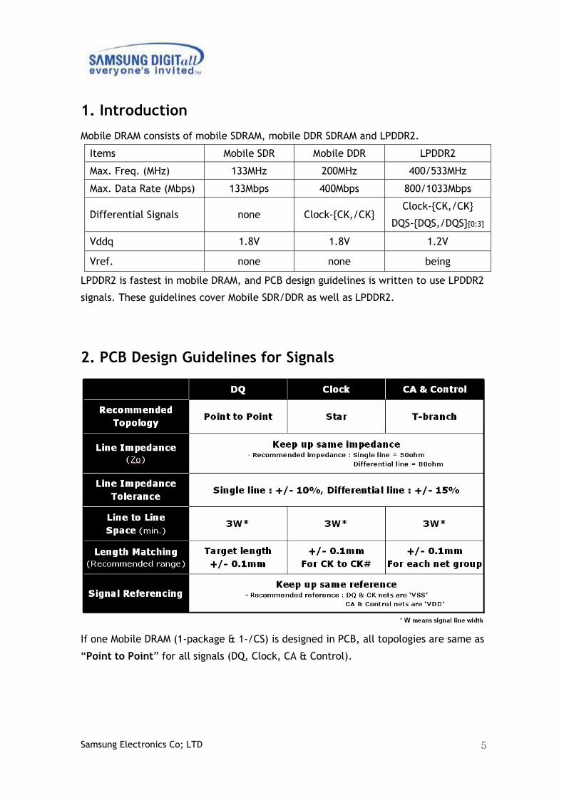
1. Introduction
Mobile DRAM consists of mobile SDRAM, mobile DDR SDRAM and LPDDR2.
Items Mobile SDR Mobile DDR LPDDR2
Max. Freq. (MHz) 133MHz 200MHz 400/533MHz
Max. Data Rate (Mbps) 133Mbps 400Mbps 800/1033Mbps
Differential Signals none Clock-{CK,/CK} Clock-{CK,/CK}
DQS-{DQS,/DQS}[0:3]
Vddq 1.8V 1.8V 1.2V
Vref. none none being
LPDDR2 is fastest in mobile DRAM, and PCB design guidelines is written to use LPDDR2
signals. These guidelines cover Mobile SDR/DDR as well as LPDDR2.
2. PCB Design Guidelines for Signals
If one Mobile DRAM (1-package & 1-/CS) is designed in PCB, all topologies are same as
“Point to Point” for all signals (DQ, Clock, CA & Control).
Samsung Electronics Co; LTD 6
2.1 DQ net design guidelines
In LPDDR2, DQ net consists of Single line(DQs) and Differential line(DQSs, /DQSs).
In mobile SDR/DDR, DQ net consists of Single line(DQs, DQSs)
P-to-P(Point to Point) topology is recommended for DQ net.
In two packages of DRAM, P-to-2P topology is recommended for DQ net
Line Length & Impedance Matching
• Check whether DQ line impedance is same for all signal layers.
Recommended DQ line impedance : 50 ohm +/- 10%
• Spacing between DQ signals is recommended to 3W.
(W means signal line width)
• Segments of DQS and /DQS should be in same layer.
Route most segments in inner layer. (if PCB has inner signal layers.)
Recommended differential impedance for DQS,/DQS : 80 ohm +/- 15%
cf.) In DDR, recommended DQS line impedance : 50 ohm +/- 10%
In mobile SDR, there is no DQS signal.
• Lengths of DQ, DQS, /DQS and DM in a byte should be in target range.
Recommended range : target length +/- 0.1mm
Example)
Lengths of DQ[0:7], DQS0, /DQS0, DM0 : 2cm +/- 0.1mm
Lengths of DQ[8:15], DQS1, /DQS1, DM1 : 2.5cm +/- 0.1mm
• Use same number of vias in DQ net or compensate length of vias.
Signal Referencing
• Signals of DQ net should keep up reference.
• Check whether DQ net has reference
(Recommended reference is VSS plane)
2.2 Clock net design guidelines
DDR and LPDDR2 have Clock and Clock# signal, but SDR has only Clock signal.
DDR and LPDDR2 should follow these Clock net design guidelines.
Star topology is recommended for clock net.
Line Length & Impedance Matching
• Check whether Clock line impedance is same for all signal layers.
Recommended differential impedance for clock net : 80 ohm +/- 15%
• Spacing between Clock net and other net is recommended to 3W.
(W means signal line width)
• Segments of Clock and Clock# should be in same layer.
Samsung Electronics Co; LTD 7
Route most clock nets in inner layer
• Length of Clock is same as length of Clock#.
Recommended range : +/- 0.1mm for CK to /CK
• Minimize the branch length.
Signal Referencing
• Signals of Clock net should keep up reference.
• Check whether Clock net has reference.
(Recommended reference is VSS plane)
2.3 CA & Control net design guidelines
In LPDDR2, CA net is DDR type (meaningful state is made by clock rising /falling edge)
and Control net is SDR type (meaningful state is made by clock rising edge).
In SDR/DDR, Command, Address net and Control net are SDR type.
T-Branch topology is recommended for Command, Address and Control net.
• CA net : CA[9:0]
• Control net : CKE, /CS
cf.) In SDR/DDR,
Command, Address net : A[15:0], BA[2:0], /RAS, /CAS, /WE
Control net : CKE, /CS
Line Length & Impedance Matching
• Check whether CA & Control impedances are same for all signal layers.
Recommended C/A & Control line impedances : 50 ohm +/- 10%
• Do not route signals near high speed signals(CK,DQ net) or have enough
spacing over 3W. (W means signal line width)
• Route most segments in inner layer. (if PCB has inner signal layers)
• Lengths of CA and Control in each net group should be in target range.
Recommended range : +/- 0.1mm for each net group
• Minimize the branch length.
Signal Referencing
• Signals of CA & Control net should keep up reference.
• Check whether C/A & Clock net have reference.
(Recommended reference is VDD plane)
Samsung Electronics Co; LTD 8
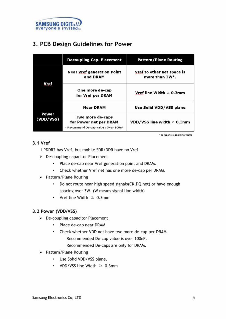
3. PCB Design Guidelines for Power
3.1 Vref
LPDDR2 has Vref, but mobile SDR/DDR have no Vref.
De-coupling capacitor Placement
• Place de-cap near Vref generation point and DRAM.
• Check whether Vref net has one more de-cap per DRAM.
Pattern/Plane Routing
• Do not route near high speed signals(CK,DQ net) or have enough
spacing over 3W. (W means signal line width)
• Vref line Width ≥ 0.3mm
3.2 Power (VDD/VSS)
De-coupling capacitor Placement
• Place de-cap near DRAM.
• Check whether VDD net have two more de-cap per DRAM.
Recommended De-cap value is over 100nF.
Recommended De-caps are only for DRAM.
Pattern/Plane Routing
• Use Solid VDD/VSS plane.
• VDD/VSS line Width ≥ 0.3mm
Samsung Electronics Co; LTD 9
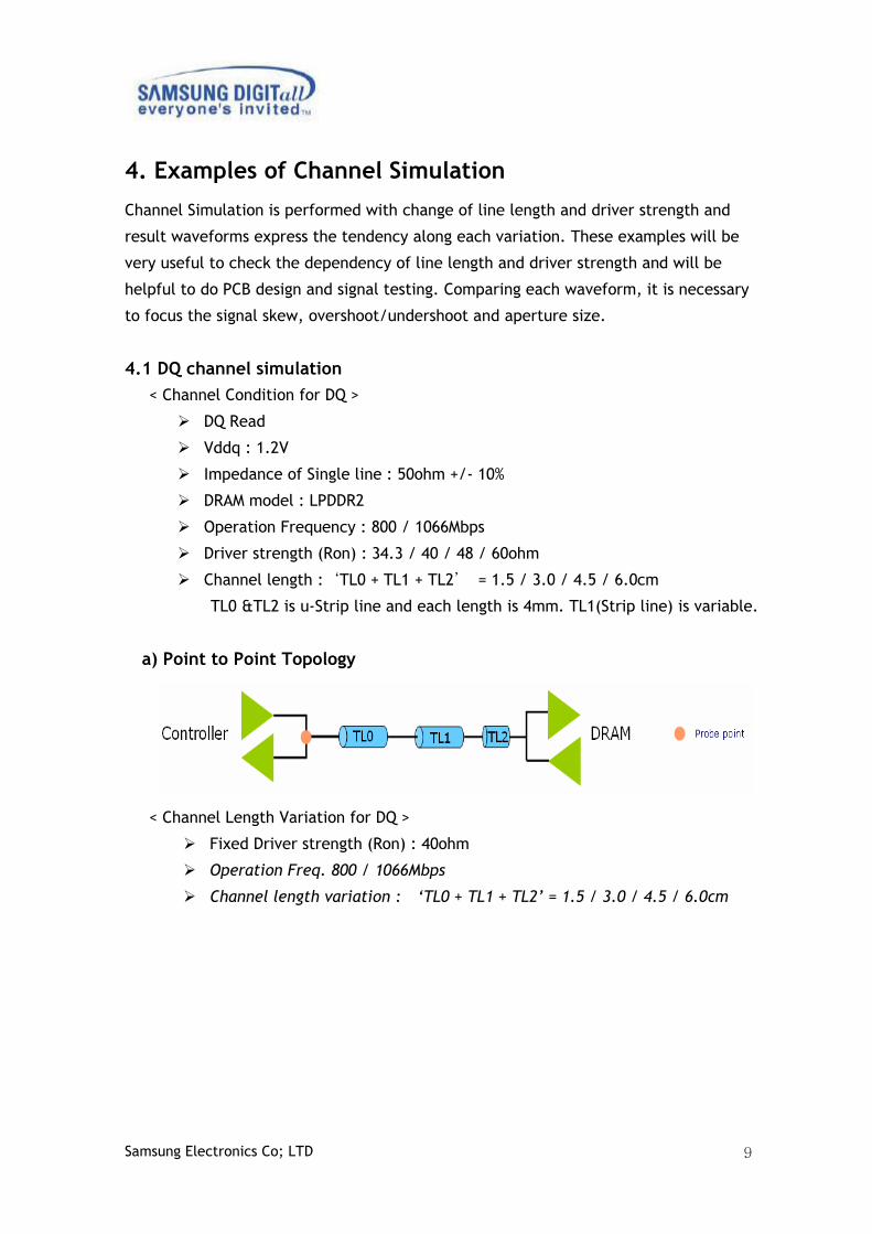
4. Examples of Channel Simulation
Channel Simulation is performed with change of line length and driver strength and
result waveforms express the tendency along each variation. These examples will be
very useful to check the dependency of line length and driver strength and will be
helpful to do PCB design and signal testing. Comparing each waveform, it is necessary
to focus the signal skew, overshoot/undershoot and aperture size.
4.1 DQ channel simulation
< Channel Condition for DQ >
DQ Read
Vddq : 1.2V
Impedance of Single line : 50ohm +/- 10%
DRAM model : LPDDR2
Operation Frequency : 800 / 1066Mbps
Driver strength (Ron) : 34.3 / 40 / 48 / 60ohm
Channel length :‘TL0 + TL1 + TL2’ = 1.5 / 3.0 / 4.5 / 6.0cm
TL0 &TL2 is u-Strip line and each length is 4mm. TL1(Strip line) is variable.
a) Point to Point Topology
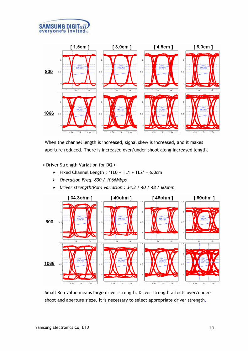
< Channel Length Variation for DQ >
Fixed Driver strength (Ron) : 40ohm
Operation Freq. 800 / 1066Mbps
Channel length variation : ‘TL0 + TL1 + TL2’ = 1.5 / 3.0 / 4.5 / 6.0cm
Samsung Electronics Co; LTD 10
When the channel length is increased, signal skew is increased, and it makes
aperture reduced. There is increased over/under-shoot along increased length.
< Driver Strength Variation for DQ >
Fixed Channel Length : „TL0 + TL1 + TL2‟ = 6.0cm
Operation Freq. 800 / 1066Mbps
Driver strength(Ron) variation : 34.3 / 40 / 48 / 60ohm
Small Ron value means large driver strength. Driver strength affects over/under-
shoot and aperture sieze. It is necessary to select appropriate driver strength.
Samsung Electronics Co; LTD 11
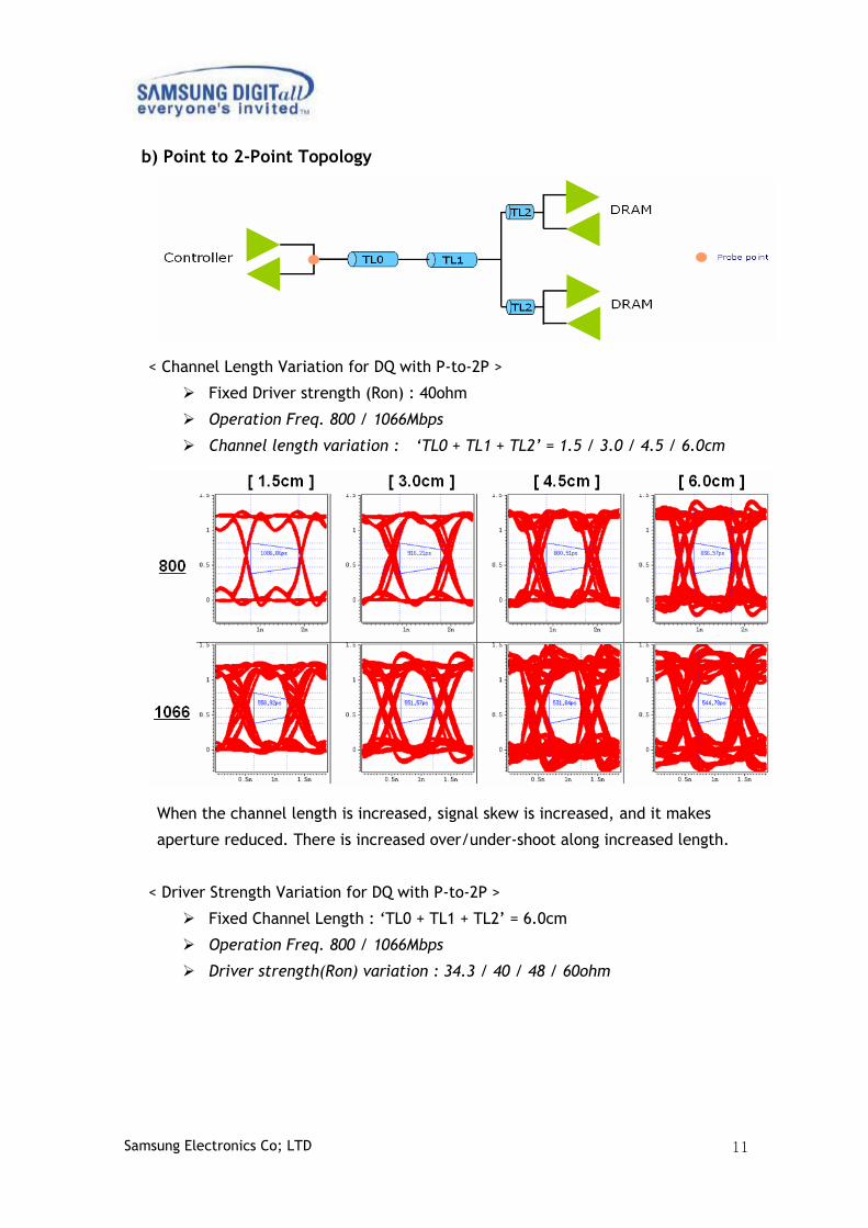
b) Point to 2-Point Topology
< Channel Length Variation for DQ with P-to-2P >
Fixed Driver strength (Ron) : 40ohm
Operation Freq. 800 / 1066Mbps
Channel length variation : ‘TL0 + TL1 + TL2’ = 1.5 / 3.0 / 4.5 / 6.0cm
When the channel length is increased, signal skew is increased, and it makes
aperture reduced. There is increased over/under-shoot along increased length.
< Driver Strength Variation for DQ with P-to-2P >
Fixed Channel Length : „TL0 + TL1 + TL2‟ = 6.0cm
Operation Freq. 800 / 1066Mbps
Driver strength(Ron) variation : 34.3 / 40 / 48 / 60ohm
Samsung Electronics Co; LTD 12
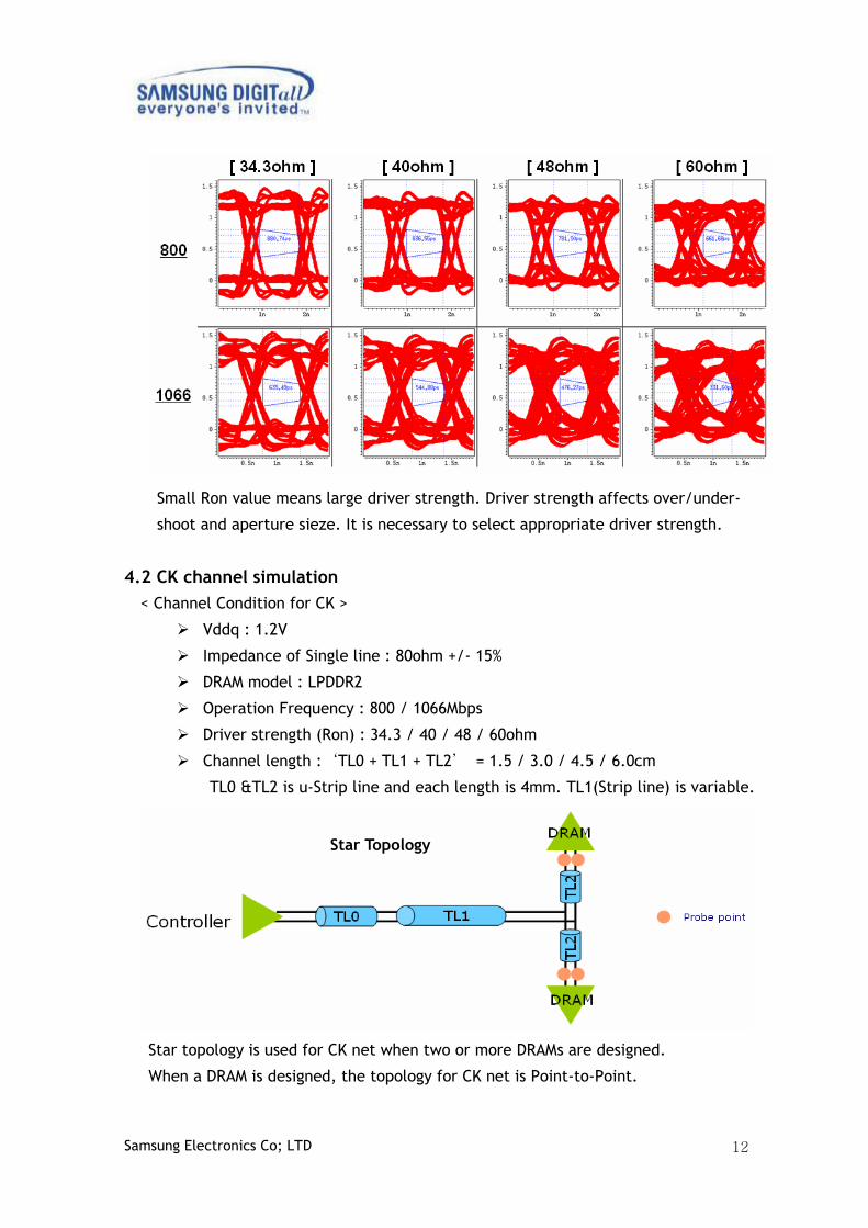
Small Ron value means large driver strength. Driver strength affects over/under-
shoot and aperture sieze. It is necessary to select appropriate driver strength.
4.2 CK channel simulation
< Channel Condition for CK >
Vddq : 1.2V
Impedance of Single line : 80ohm +/- 15%
DRAM model : LPDDR2
Operation Frequency : 800 / 1066Mbps
Driver strength (Ron) : 34.3 / 40 / 48 / 60ohm
Channel length :‘TL0 + TL1 + TL2’ = 1.5 / 3.0 / 4.5 / 6.0cm
TL0 &TL2 is u-Strip line and each length is 4mm. TL1(Strip line) is variable.
Star topology is used for CK net when two or more DRAMs are designed.
When a DRAM is designed, the topology for CK net is Point-to-Point.
Star Topology
Samsung Electronics Co; LTD 13
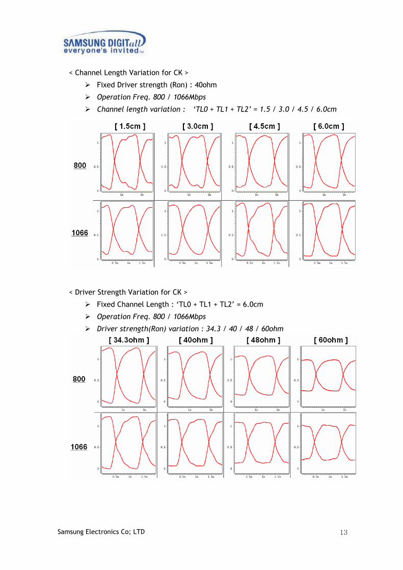
< Channel Length Variation for CK >
Fixed Driver strength (Ron) : 40ohm
Operation Freq. 800 / 1066Mbps
Channel length variation : ‘TL0 + TL1 + TL2’ = 1.5 / 3.0 / 4.5 / 6.0cm
< Driver Strength Variation for CK >
Fixed Channel Length : „TL0 + TL1 + TL2‟ = 6.0cm
Operation Freq. 800 / 1066Mbps
Driver strength(Ron) variation : 34.3 / 40 / 48 / 60ohm
Samsung Electronics Co; LTD 14
4.3 CA & Control channel simulation
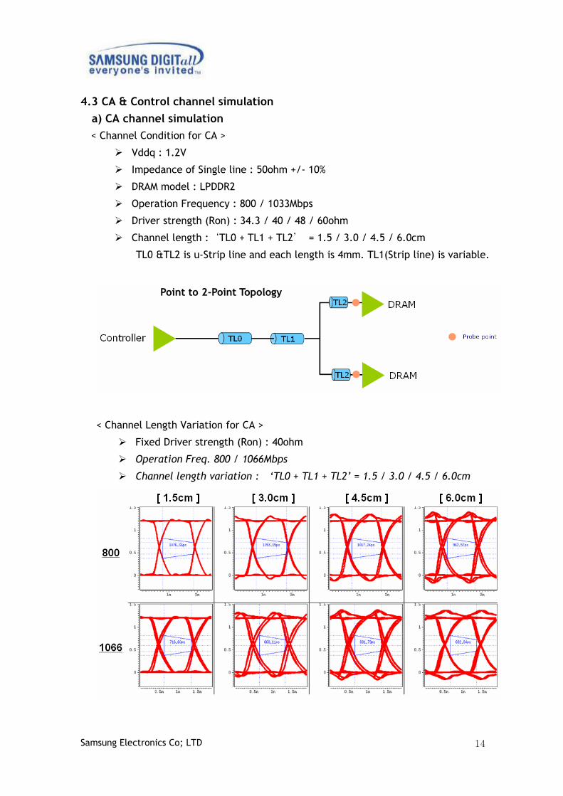
a) CA channel simulation
< Channel Condition for CA >
Vddq : 1.2V
Impedance of Single line : 50ohm +/- 10%
DRAM model : LPDDR2
Operation Frequency : 800 / 1033Mbps
Driver strength (Ron) : 34.3 / 40 / 48 / 60ohm
Channel length :‘TL0 + TL1 + TL2’ = 1.5 / 3.0 / 4.5 / 6.0cm
TL0 &TL2 is u-Strip line and each length is 4mm. TL1(Strip line) is variable.
< Channel Length Variation for CA >
Fixed Driver strength (Ron) : 40ohm
Operation Freq. 800 / 1066Mbps
Channel length variation : ‘TL0 + TL1 + TL2’ = 1.5 / 3.0 / 4.5 / 6.0cm
Point to 2-Point Topology
Samsung Electronics Co; LTD 15
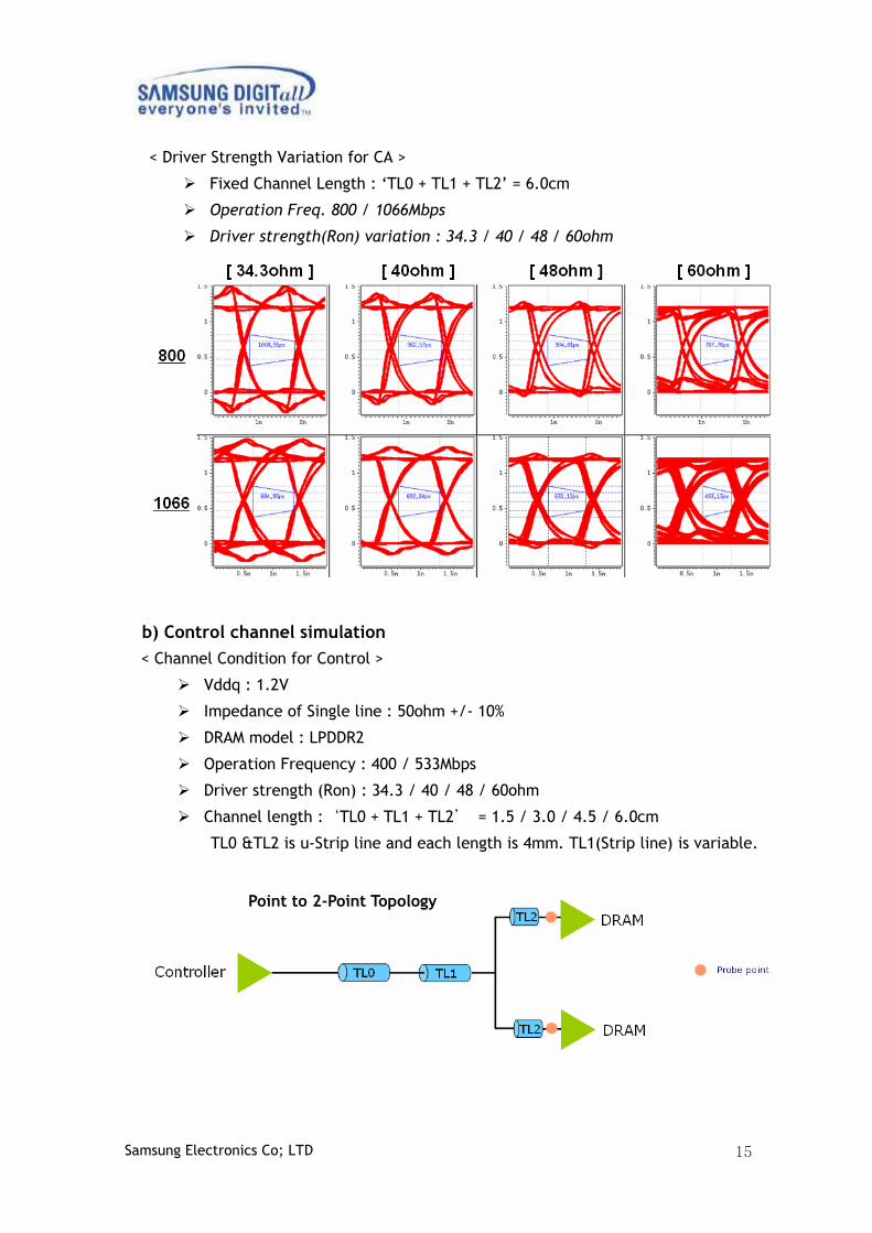
< Driver Strength Variation for CA >
Fixed Channel Length : „TL0 + TL1 + TL2‟ = 6.0cm
Operation Freq. 800 / 1066Mbps
Driver strength(Ron) variation : 34.3 / 40 / 48 / 60ohm
b) Control channel simulation
< Channel Condition for Control >
Vddq : 1.2V
Impedance of Single line : 50ohm +/- 10%
DRAM model : LPDDR2
Operation Frequency : 400 / 533Mbps
Driver strength (Ron) : 34.3 / 40 / 48 / 60ohm
Channel length :‘TL0 + TL1 + TL2’ = 1.5 / 3.0 / 4.5 / 6.0cm
TL0 &TL2 is u-Strip line and each length is 4mm. TL1(Strip line) is variable.
Point to 2-Point Topology
Samsung Electronics Co; LTD 16
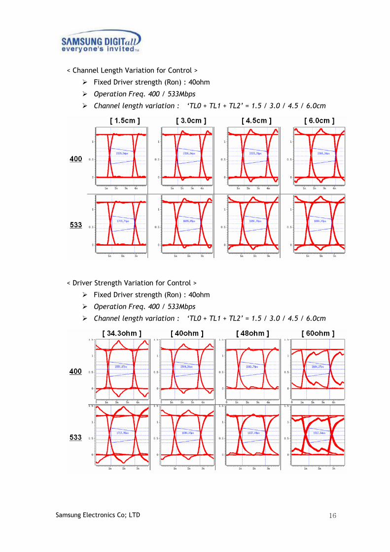
< Channel Length Variation for Control >
Fixed Driver strength (Ron) : 40ohm
Operation Freq. 400 / 533Mbps
Channel length variation : ‘TL0 + TL1 + TL2’ = 1.5 / 3.0 / 4.5 / 6.0cm
< Driver Strength Variation for Control >
Fixed Driver strength (Ron) : 40ohm
Operation Freq. 400 / 533Mbps
Channel length variation : ‘TL0 + TL1 + TL2’ = 1.5 / 3.0 / 4.5 / 6.0cm
Samsung Electronics Co; LTD 17
4.4 Channel Simulation Summary
Summary of DQ @800Mbps
P-to-P(Point to Point) topology is recommended for DQ net.
Minimize the trace between driver and receiver.
• Shorter than 4.5cm to avoid overshoot/undershoot problem.
• Longer length, Larger Skew and ISI.
Appropriate Driver strength helps to reduce Overshoot/Undershoot appearance.
• Appropriate Driver strength values are recommended by Simulation.
• In case of total-length‘6cm’, the best driver strength is‘Ron
40ohm’condition.
Summary of CA, Control & Clock @800Mbps
Minimize the trace between driver and receiver.
• Shorter than 3cm to avoid overshoot/undershoot problem.
Appropriate Driver strength helps to reduce Overshoot/Undershoot appearance.
• Appropriate Driver strength values are recommended by Simulation.
• In case of total-length‘6cm’, the best driver strength is‘Ron
48ohm’condition.