Embed Size (px)
Citation preview
DAI 0385C Copyright 2015 ARM. All rights reserved. iAN385 Non-Confidential
Application Note AN385ARM® Cortex®-M3 SMM on V2M-MPS2
Non-Confidential
DAI 0385C Copyright 2015 ARM. All rights reserved. iiAN385 Non-Confidential
ARM® Cortex®-M3 SMM on V2M-MPS2
Copyright © 2015 ARM. All rights reserved.
Release Information
The following changes have been made to this Application Note.
Change History
Date Issue Confidentiality Change
12 December 2013 A Non-Confidential First release
1 November 2014 B Non-Confidential Corrected MCC switch register address
02 December 2015 C Non-Confidential External shield support added
Non-Confidential Proprietary Notice
This document is protected by copyright and other related rights and the practice or implementation of the informationcontained in this document may be protected by one or more patents or pending patent applications. No part of thisdocument may be reproduced in any form by any means without the express prior written permission of ARM. Nolicense, express or implied, by estoppel or otherwise to any intellectual property rights is granted by thisdocument unless specifically stated.
Your access to the information in this document is conditional upon your acceptance that you will not use or permitothers to use the information for the purposes of determining whether implementations infringe any third party patents.
THIS DOCUMENT IS PROVIDED “AS IS”. ARM PROVIDES NO REPRESENTATIONS AND NO WARRANTIES,EXPRESS, IMPLIED OR STATUTORY, INCLUDING, WITHOUT LIMITATION, THE IMPLIED WARRANTIES OFMERCHANTABILITY, SATISFACTORY QUALITY, NON-INFRINGEMENT OR FITNESS FOR A PARTICULARPURPOSE WITH RESPECT TO THE DOCUMENT. For the avoidance of doubt, ARM makes no representation withrespect to, and has undertaken no analysis to identify or understand the scope and content of, third party patents,copyrights, trade secrets, or other rights.
This document may include technical inaccuracies or typographical errors.
TO THE EXTENT NOT PROHIBITED BY LAW, IN NO EVENT WILL ARM BE LIABLE FOR ANY DAMAGES,INCLUDING WITHOUT LIMITATION ANY DIRECT, INDIRECT, SPECIAL, INCIDENTAL, PUNITIVE, ORCONSEQUENTIAL DAMAGES, HOWEVER CAUSED AND REGARDLESS OF THE THEORY OF LIABILITY,ARISING OUT OF ANY USE OF THIS DOCUMENT, EVEN IF ARM HAS BEEN ADVISED OF THE POSSIBILITY OFSUCH DAMAGES.
This document consists solely of commercial items. You shall be responsible for ensuring that any use, duplication ordisclosure of this document complies fully with any relevant export laws and regulations to assure that this documentor any portion thereof is not exported, directly or indirectly, in violation of such export laws. Use of the word “partner” inreference to ARM’s customers is not intended to create or refer to any partnership relationship with any othercompany. ARM may make changes to this document at any time and without notice.
If any of the provisions contained in these terms conflict with any of the provisions of any signed written agreementcovering this document with ARM, then the signed written agreement prevails over and supersedes the conflictingprovisions of these terms. This document may be translated into other languages for convenience, and you agree thatif there is any conflict between the English version of this document and any translation, the terms of the Englishversion of the Agreement shall prevail.
Words and logos marked with ® or ™ are registered trademarks or trademarks of ARM Limited or its affiliates in the EUand/or elsewhere. All rights reserved. Other brands and names mentioned in this document may be the trademarks oftheir respective owners. Please follow ARM’s trademark usage guidelines at http://www.arm.com/about/trademark-usage-guidelines.php
Copyright © [2015], ARM Limited or its affiliates. All rights reserved.
ARM Limited. Company 02557590 registered in England.
110 Fulbourn Road, Cambridge, England CB1 9NJ.
LES-PRE-20349
DAI 0385C Copyright 2015 ARM. All rights reserved. iiiAN385 Non-Confidential
Contents
ARM® Cortex®-M3 SMM on V2M-MPS21 Conventions and Feedback ....................................................................................1-1
2 Preface ......................................................................................................................2-1
2.1 References ..........................................................................................................2-1
2.2 Terms and abbreviations .....................................................................................2-1
2.3 Encryption key .....................................................................................................2-2
3 Overview ...................................................................................................................3-1
3.1 Memory Map........................................................................................................3-3
3.2 Block RAM for Booting ........................................................................................3-4
3.3 External ZBT Synchronous SRAM (SSRAM1)....................................................3-5
3.4 External ZBT Synchronous SRAM (SSRAM2 & SSRAM3) ................................3-5
3.5 External PSRAM..................................................................................................3-5
3.6 CMSDK APB subsystem .....................................................................................3-5
3.7 AHB GPIO ...........................................................................................................3-6
3.8 SPI (Serial Peripheral Interface)..........................................................................3-6
3.9 Color LCD parallel interface ................................................................................3-7
3.10 Ethernet ...............................................................................................................3-7
3.11 VGA .....................................................................................................................3-7
3.12 Audio I2S..............................................................................................................3-7
3.13 Audio Configuration .............................................................................................3-9
3.14 FPGA system control and I/O..............................................................................3-9
4 Clocks .......................................................................................................................4-1
5 Interrupt assignments .............................................................................................5-1
6 Serial Communication Controller (SCC)................................................................6-1
7 Shield Support..........................................................................................................7-3
DAI 0385C Copyright 2015 ARM. All rights reserved. 1-1AN385 Non-Confidential
1 Conventions and Feedback
The following describes the typographical conventions and how to give feedback:
Typographical conventions
The following typographical conventions are used:
monospace denotes text that you can enter at the keyboard, such as commands, file andprogram names, and source code.
monospace denotes a permitted abbreviation for a command or option. You can enterthe underlined text instead of the full command or option name.
monospace italic
denotes arguments to commands and functions where the argument is to bereplaced by a specific value.
monospace bold
denotes language keywords when used outside example code.
italic highlights important notes, introduces special terminology, denotes internalcross-references, and citations.
bold highlights interface elements, such as menu names. Denotes signal names.Also used for emphasis in descriptive lists, where appropriate.
Feedback on this product
If you have any comments and suggestions about this product, contact your supplier and give:
Your name and company.
The serial number of the product.
Details of the release you are using.
Details of the platform you are using, such as the hardware platform, operating system type andversion.
A small standalone sample of code that reproduces the problem.
A clear explanation of what you expected to happen, and what actually happened.
The commands you used, including any command-line options.
Sample output illustrating the problem.
The version string of the tools, including the version number and build numbers.
Feedback on documentation
If you have comments on the documentation, e-mail [email protected]. Give:
The title.
The number, DAI0385C.
If viewing online, the topic names to which your comments apply.
If viewing a PDF version of a document, the page numbers to which your comments apply.
A concise explanation of your comments.
ARM also welcomes general suggestions for additions and improvements.
DAI 0385C Copyright 2015 ARM. All rights reserved. 1-2AN385 Non-Confidential
ARM periodically provides updates and corrections to its documentation on the ARM InformationCenter, together with knowledge articles and Frequently Asked Questions (FAQs).
Other information
ARM Information Center, http://infocenter.arm.com/help/index.jsp.
ARM Technical Support Knowledge Articles,http://infocenter.arm.com/help/topic/com.arm.doc.faqs/index.html.
ARM Support and Maintenance, http://www.arm.com/support/services/support-maintenance.php.
ARM Glossary, http://infocenter.arm.com/help/topic/com.arm.doc.aeg0014-/index.html.
The ARM Glossary is a list of terms used in ARM documentation, together with definitions forthose terms. The ARM Glossary does not contain terms that are industry standard unless the ARMmeaning differs from the generally accepted meaning.
DAI 0385C Copyright 2015 ARM. All rights reserved. 2-1AN385 Non-Confidential
2 Preface
This SMM is intended for developers and programmers for deployment of hardware or software.
These topics support the following chapters:
References on page 2-1.
Terms and abbreviations on page 2-1.
Encryption key on page 2-2
2.1 References
ARMv7-M Architecture Reference Manual ARMv7-A and ARMv7-R edition (ARM DDI 0403D)for Cortex-M productshttp://infocenter.arm.com/help/topic/com.arm.doc.ddi0403c/index.html
ARM® Versatile™ Express Cortex®-M Prototyping System (V2M-MPS2)Technical ReferenceManual
Cortex®-M System Design Kit
http://www.arm.com/products/processors/cortex-m/cortex-m-system-design-kit.php
The Cortex®-M System Design Kit (CMSDK) is a product to help silicon and FPGA designersto create Cortex-M based systems. It contains ready-to-use example systems for Cortex-Mprocessors and a range of AMBA® bus fabric components for Cortex-M system development.
Cortex®-M System Design Kit Technical Reference Manualhttp://infocenter.arm.com/help/topic/com.arm.doc.ddi0479c/index.html
ARM® PrimeCell Synchronous Serial Port (PL022) Technical Reference Manualhttp://infocenter.arm.com/help/index.jsp?topic=/com.arm.doc.ddi0194g/ I1005344.html
Keil® MCBSTM32C Evaluation Board Display Board Schematichttp://www.keil.com/mcbstm32c/mcbstm32c-display-board-schematics.pdf
ARM V2M-Shield1 Technical Reference Manualhttp://infocenter.arm.com/insert/link/here.pdf
2.2 Terms and abbreviations
Volatile (storage class qualifier)In C and C++ this is the volatile storage class qualifier. In other languages thesyntax and semantics might vary slightly if the concept is supported at all.The intent is to cover all storage locations that might be used for inter-processor communication variables that can be used for lock-freeprogramming.
CMSDK Cortex-M System Design Kit.
MCC Motherboard Configuration Controller
DAI 0385C Copyright 2015 ARM. All rights reserved. 2-2AN385 Non-Confidential
2.3 Encryption key
ARM supplies the V2M-MPS2 motherboard with a decryption key programmed into the FPGA.This key is needed to enable loading of the prebuilt images, which are encrypted.
Caution
A battery supplies power to the key storage area of the FPGA. Any keys stored in the FPGAmight be lost when battery power is lost. If this happens you must return the board to ARM forreprogramming of the key.
DAI 0385C Copyright 2015 ARM. All rights reserved. 3-1AN385 Non-Confidential
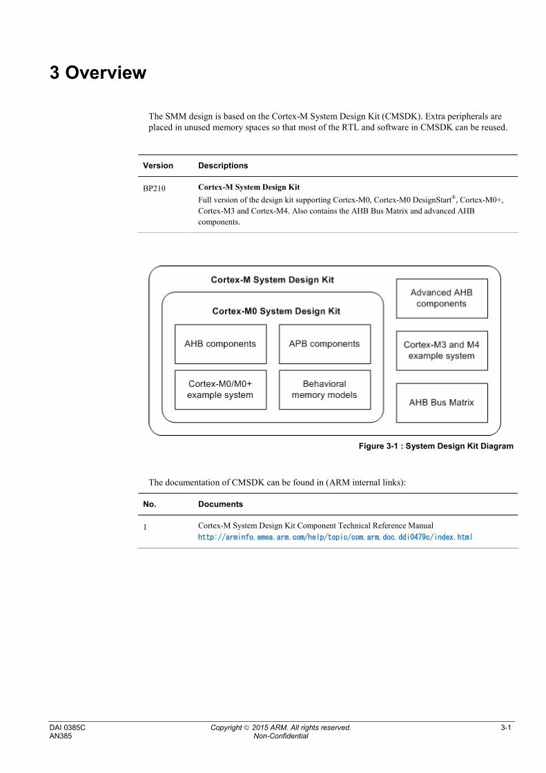
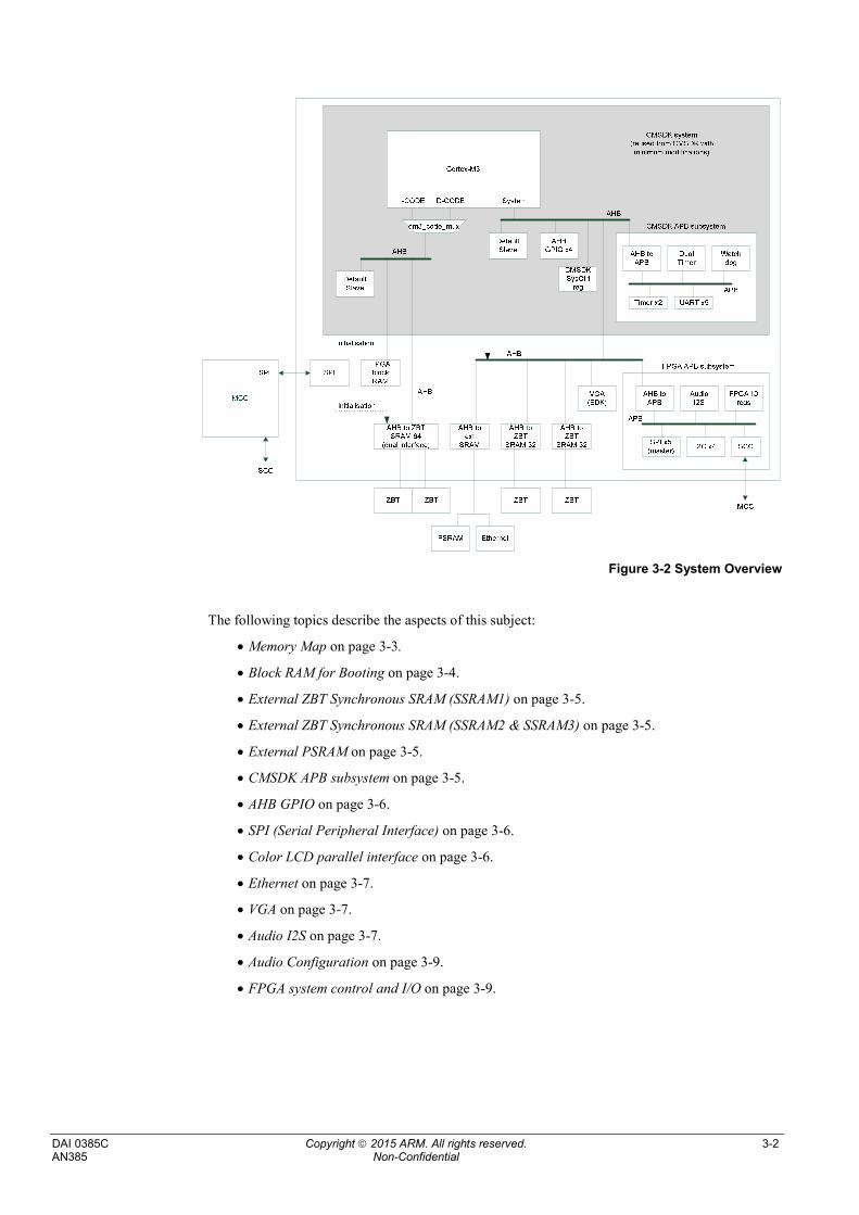
3 Overview
The SMM design is based on the Cortex-M System Design Kit (CMSDK). Extra peripherals areplaced in unused memory spaces so that most of the RTL and software in CMSDK can be reused.
Version Descriptions
BP210 Cortex-M System Design Kit
Full version of the design kit supporting Cortex-M0, Cortex-M0 DesignStart®, Cortex-M0+,
Cortex-M3 and Cortex-M4. Also contains the AHB Bus Matrix and advanced AHB
components.
Figure 3-1 : System Design Kit Diagram
The documentation of CMSDK can be found in (ARM internal links):
No. Documents
1 Cortex-M System Design Kit Component Technical Reference Manual
http://arminfo.emea.arm.com/help/topic/com.arm.doc.ddi0479c/index.html
DAI 0385C Copyright 2015 ARM. All rights reserved. 3-2AN385 Non-Confidential
Figure 3-2 System Overview
The following topics describe the aspects of this subject:
Memory Map on page 3-3.
Block RAM for Booting on page 3-4.
External ZBT Synchronous SRAM (SSRAM1) on page 3-5.
External ZBT Synchronous SRAM (SSRAM2 & SSRAM3) on page 3-5.
External PSRAM on page 3-5.
CMSDK APB subsystem on page 3-5.
AHB GPIO on page 3-6.
SPI (Serial Peripheral Interface) on page 3-6.
Color LCD parallel interface on page 3-6.
Ethernet on page 3-7.
VGA on page 3-7.
Audio I2S on page 3-7.
Audio Configuration on page 3-9.
FPGA system control and I/O on page 3-9.
DAI 0385C Copyright 2015 ARM. All rights reserved. 3-3AN385 Non-Confidential
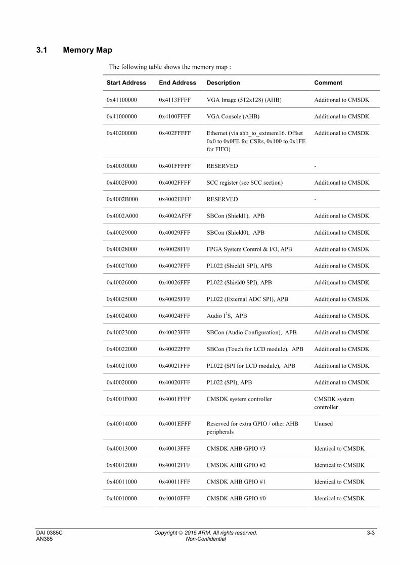
3.1 Memory Map
The following table shows the memory map :
Start Address End Address Description Comment
0x41100000 0x4113FFFF VGA Image (512x128) (AHB) Additional to CMSDK
0x41000000 0x4100FFFF VGA Console (AHB) Additional to CMSDK
0x40200000 0x402FFFFF Ethernet (via ahb_to_extmem16. Offset
0x0 to 0x0FE for CSRs, 0x100 to 0x1FE
for FIFO)
Additional to CMSDK
0x40030000 0x401FFFFF RESERVED -
0x4002F000 0x4002FFFF SCC register (see SCC section) Additional to CMSDK
0x4002B000 0x4002EFFF RESERVED -
0x4002A000 0x4002AFFF SBCon (Shield1), APB Additional to CMSDK
0x40029000 0x40029FFF SBCon (Shield0), APB Additional to CMSDK
0x40028000 0x40028FFF FPGA System Control & I/O, APB Additional to CMSDK
0x40027000 0x40027FFF PL022 (Shield1 SPI), APB Additional to CMSDK
0x40026000 0x40026FFF PL022 (Shield0 SPI), APB Additional to CMSDK
0x40025000 0x40025FFF PL022 (External ADC SPI), APB Additional to CMSDK
0x40024000 0x40024FFF Audio I2S, APB Additional to CMSDK
0x40023000 0x40023FFF SBCon (Audio Configuration), APB Additional to CMSDK
0x40022000 0x40022FFF SBCon (Touch for LCD module), APB Additional to CMSDK
0x40021000 0x40021FFF PL022 (SPI for LCD module), APB Additional to CMSDK
0x40020000 0x40020FFF PL022 (SPI), APB Additional to CMSDK
0x4001F000 0x4001FFFF CMSDK system controller CMSDK system
controller
0x40014000 0x4001EFFF Reserved for extra GPIO / other AHB
peripherals
Unused
0x40013000 0x40013FFF CMSDK AHB GPIO #3 Identical to CMSDK
0x40012000 0x40012FFF CMSDK AHB GPIO #2 Identical to CMSDK
0x40011000 0x40011FFF CMSDK AHB GPIO #1 Identical to CMSDK
0x40010000 0x40010FFF CMSDK AHB GPIO #0 Identical to CMSDK
DAI 0385C Copyright 2015 ARM. All rights reserved. 3-4AN385 Non-Confidential
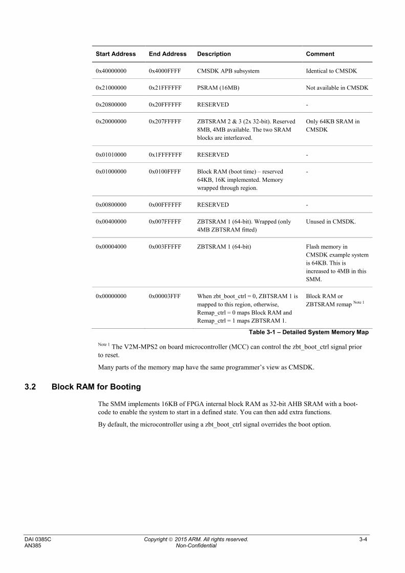
Start Address End Address Description Comment
0x40000000 0x4000FFFF CMSDK APB subsystem Identical to CMSDK
0x21000000 0x21FFFFFF PSRAM (16MB) Not available in CMSDK
0x20800000 0x20FFFFFF RESERVED -
0x20000000 0x207FFFFF ZBTSRAM 2 & 3 (2x 32-bit). Reserved
8MB, 4MB available. The two SRAM
blocks are interleaved.
Only 64KB SRAM in
CMSDK
0x01010000 0x1FFFFFFF RESERVED -
0x01000000 0x0100FFFF Block RAM (boot time) – reserved
64KB, 16K implemented. Memory
wrapped through region.
-
0x00800000 0x00FFFFFF RESERVED -
0x00400000 0x007FFFFF ZBTSRAM 1 (64-bit). Wrapped (only
4MB ZBTSRAM fitted)
Unused in CMSDK.
0x00004000 0x003FFFFF ZBTSRAM 1 (64-bit) Flash memory in
CMSDK example system
is 64KB. This is
increased to 4MB in this
SMM.
0x00000000 0x00003FFF When zbt_boot_ctrl = 0, ZBTSRAM 1 is
mapped to this region, otherwise,
Remap_ctrl = 0 maps Block RAM and
Remap_ctrl = 1 maps ZBTSRAM 1.
Block RAM or
ZBTSRAM remap Note 1
Table 3-1 – Detailed System Memory Map
Note 1 The V2M-MPS2 on board microcontroller (MCC) can control the zbt_boot_ctrl signal priorto reset.
Many parts of the memory map have the same programmer’s view as CMSDK.
3.2 Block RAM for Booting
The SMM implements 16KB of FPGA internal block RAM as 32-bit AHB SRAM with a boot-code to enable the system to start in a defined state. You can then add extra functions.
By default, the microcontroller using a zbt_boot_ctrl signal overrides the boot option.
DAI 0385C Copyright 2015 ARM. All rights reserved. 3-5AN385 Non-Confidential
3.3 External ZBT Synchronous SRAM (SSRAM1)
This section describes the Fast Program SRAM in the CODE region.
This is interfaced to two external 32-bit ZBT SSRAM in parallel, forming a 64-bit ZBT SSRAM.8MB of memory space are allocated, but only 4MB is used (each ZBT SSRAM is 2MB).
By default, the first 64KB is aliased to the FPGA internal block RAM. You can turn off thealiasing by clearing the REMAP register in the CMSDK system controller. By default, the SMMdesign overwrites this alias with an additional boot control so that it boots from ZBT SRAM.
CMSDK_SYSCON->REMAP = 0;
You can also turn this off by changing the TOTALSYSCONS variable in the board.txt file to 0.
TOTALSYSCONS: 1 -> TOTALSYSCONS: 0
This memory space connects through AHB.
3.4 External ZBT Synchronous SRAM (SSRAM2 & SSRAM3)
The Fast ZBT SSRAM in SRAM region is set up as two external ZBT SSRAMs, connected to twoindependent ZBT interfaces. In the 8MB memory region, 4MB of ZBT is available.
The address of the ZBT SSRAM is interleaved as shown in the table below.
Upper 32-bit ZBT SSRAM3 Lower 32-bit ZBT SSRAM2
0x207FFFFC (wrap round to 0x203FFFFC) 0x207FFFF8 (wrap round to 0x203FFFF8)
… …
0x20400004 (wrap round to 0x20000004) 0x20200000 (wrap round to 0x20000000)
0x203FFFFC 0x203FFFF8
… …
0x2000000C 0x20000008
0x20000004 0x20000000Table 3-2 – 32 bit ZBT Memory Map
This memory space connects through AHB.
3.5 External PSRAM
A 16MB 16-bit PSRAM area is available and the memory map allocates the address-range0x21000000 -0x21FFFFFF. This enables large test programs to be used, for example uClinux, inthe SRAM region of the Cortex-M memory space.
Note: Running code from SRAM region is slower than from CODE region because the internal busstructure is not optimized for running programs from this region.
3.6 CMSDK APB subsystem
The SMM uses APB subsystem in CMSDK.
Address Item Notes
0x4000F000-0x4000FFFF APB expansion port 15 Not used. Reserved for micro
DMA controller configuration
port
0x4000E000-0x4000EFFF APB expansion port 14 Not used
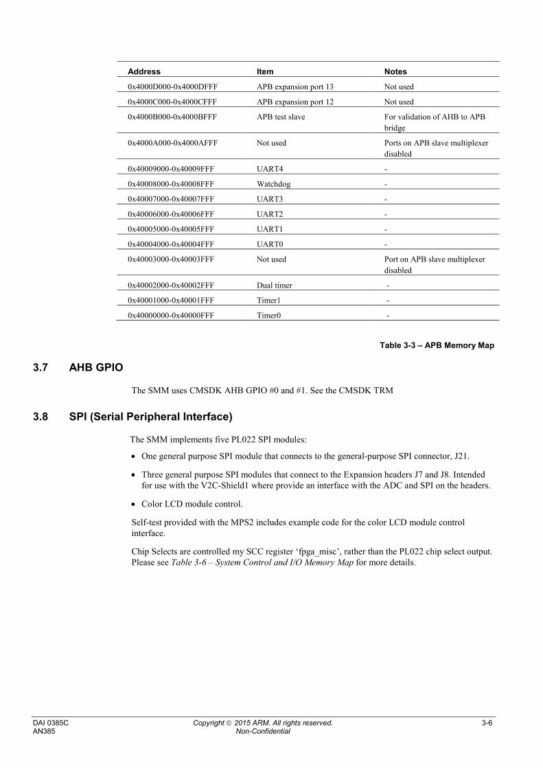
DAI 0385C Copyright 2015 ARM. All rights reserved. 3-6AN385 Non-Confidential
Address Item Notes
0x4000D000-0x4000DFFF APB expansion port 13 Not used
0x4000C000-0x4000CFFF APB expansion port 12 Not used
0x4000B000-0x4000BFFF APB test slave For validation of AHB to APB
bridge
0x4000A000-0x4000AFFF Not used Ports on APB slave multiplexer
disabled
0x40009000-0x40009FFF UART4 -
0x40008000-0x40008FFF Watchdog -
0x40007000-0x40007FFF UART3 -
0x40006000-0x40006FFF UART2 -
0x40005000-0x40005FFF UART1 -
0x40004000-0x40004FFF UART0 -
0x40003000-0x40003FFF Not used Port on APB slave multiplexer
disabled
0x40002000-0x40002FFF Dual timer -
0x40001000-0x40001FFF Timer1 -
0x40000000-0x40000FFF Timer0 -
Table 3-3 – APB Memory Map
3.7 AHB GPIO
The SMM uses CMSDK AHB GPIO #0 and #1. See the CMSDK TRM
3.8 SPI (Serial Peripheral Interface)
The SMM implements five PL022 SPI modules:
One general purpose SPI module that connects to the general-purpose SPI connector, J21.
Three general purpose SPI modules that connect to the Expansion headers J7 and J8. Intendedfor use with the V2C-Shield1 where provide an interface with the ADC and SPI on the headers.
Color LCD module control.
Self-test provided with the MPS2 includes example code for the color LCD module controlinterface.
Chip Selects are controlled my SCC register ‘fpga_misc’, rather than the PL022 chip select output.Please see Table 3-6 – System Control and I/O Memory Map for more details.
DAI 0385C Copyright 2015 ARM. All rights reserved. 3-7AN385 Non-Confidential
3.9 Color LCD parallel interface
The color LCD module has two interfaces:
SPI for LCD module used for sending image data to the LCD.
I2C for touch used to transfer data input via the touch screen.
These interfaces are connected to a STMicroelectronics STMPE811QTR Port Expander withAdvanced Touch Screen Controller on the Keil MCBSTM32C display board. (Schematic listed inthe reference section).
Self-test provided with the MPS2 includes example code for both of these interfaces.
3.10 Ethernet
The SMM design connects SMSC LAN9220 through AHB to external memory block.
The SMM self-test code includes example code for a simple loopback operation.
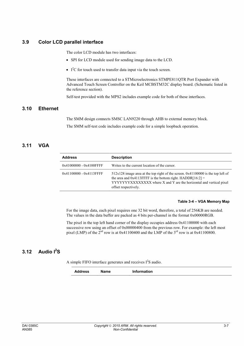
3.11 VGA
Address Description
0x41000000 - 0x4100FFFF Writes to the current location of the cursor.
0x41100000 - 0x4113FFFF 512x128 image area at the top right of the screen. 0x41100000 is the top left ofthe area and 0x4113FFFF is the bottom right. HADDR[16:2] =YYYYYYYXXXXXXXX where X and Y are the horizontal and vertical pixeloffset respectively.
Table 3-4 – VGA Memory Map
For the image data, each pixel requires one 32 bit word, therefore, a total of 256KB are needed.The values in the data buffer are packed as 4 bits per-channel in the format 0x00000RGB.
The pixel in the top left hand corner of the display occupies address 0x41100000 with eachsuccessive row using an offset of 0x00000400 from the previous row. For example: the left mostpixel (LMP) of the 2nd row is at 0x41100400 and the LMP of the 3rd row is at 0x41100800.
3.12 Audio I2S
A simple FIFO interface generates and receives I2S audio.
Address Name Information
DAI 0385C Copyright 2015 ARM. All rights reserved. 3-8AN385 Non-Confidential
Address Name Information
0x40024000 CONTROL Control Register
[31:18] : Reserved
[17] : Audio CODEC reset control (output pin)
[16] : FIFO reset
[15] : Reserved
[14:12] : RX Buffer IRQ Water Level - Default 2
(IRQ triggers when more less 2 word space available)
[11] : Reserved
[10: 8] : TX Buffer IRQ Water Level - Default 2
(IRQ triggers when more than 2 word space available)
[7: 4] : Reserved
[3] : RX Interrupt Enable
[2] : RX Enable
[1] : TX Interrupt Enable
[0] : TX Enable
0x40024004 STATUS Status register
[31:6] : Reserved
[5] : RX Buffer Full
[4] : RX Buffer Empty
[3] : TX Buffer Full
[2] : TX Buffer Empty
[1] : RX Buffer Alert (Depends on Water level)
[0] : TX Buffer Alert (Depends on Water level)
0x40024008 ERROR Error status register
[31:2] : Reserved
[1] : RX overrun - write 1 to clear
[0] : TX overrun/underrun - write 1 to clear
0x4002400C DIVIDE Divide ratio register (for Left/Right clock)
[31:10] : Reserved
[ 9: 0] LRDIV (Left/Right) Default = 0x80
12.288MHz / 48KHz / 2 (L+R) = 128
0x40024010 TXBUF Transmit Buffer FIFO Data Register (WO)
[31:16] : Left Channel
[15: 0] : Right Channel
0x40024014 RXBUF Receive Buffer FIFO Data Register (RO)
[31:16] Left Channel
[15: 0] Right Channel
0x40024018
–
0x400242FC
RESERVED -
DAI 0385C Copyright 2015 ARM. All rights reserved. 3-9AN385 Non-Confidential
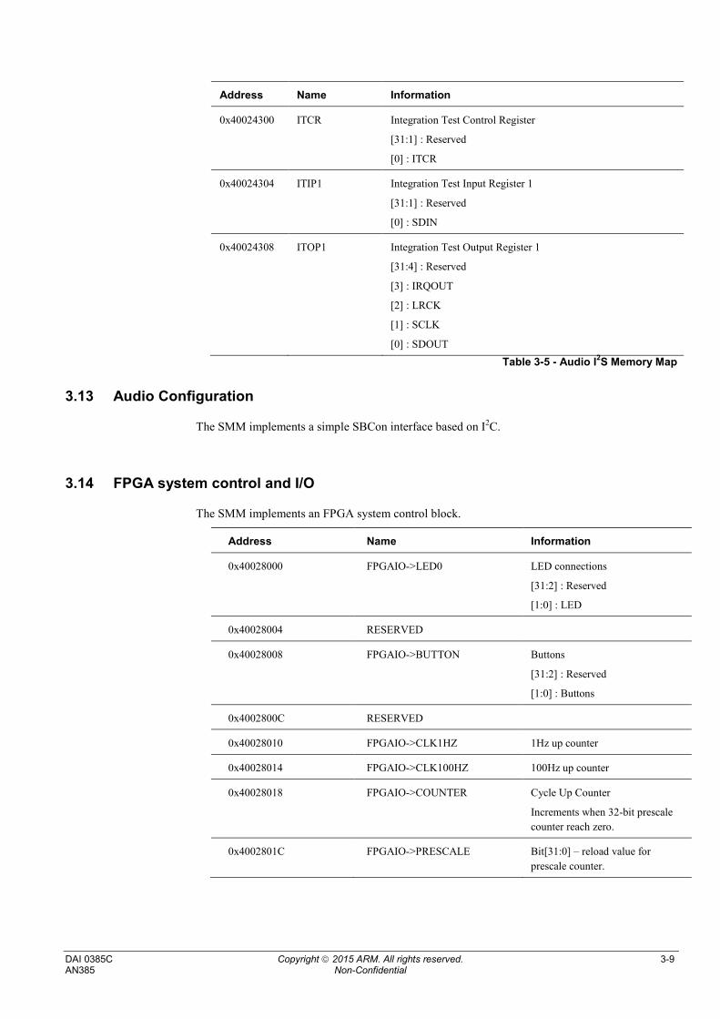
Address Name Information
0x40024300 ITCR Integration Test Control Register
[31:1] : Reserved
[0] : ITCR
0x40024304 ITIP1 Integration Test Input Register 1
[31:1] : Reserved
[0] : SDIN
0x40024308 ITOP1 Integration Test Output Register 1
[31:4] : Reserved
[3] : IRQOUT
[2] : LRCK
[1] : SCLK
[0] : SDOUT
Table 3-5 - Audio I2S Memory Map
3.13 Audio Configuration
The SMM implements a simple SBCon interface based on I2C.
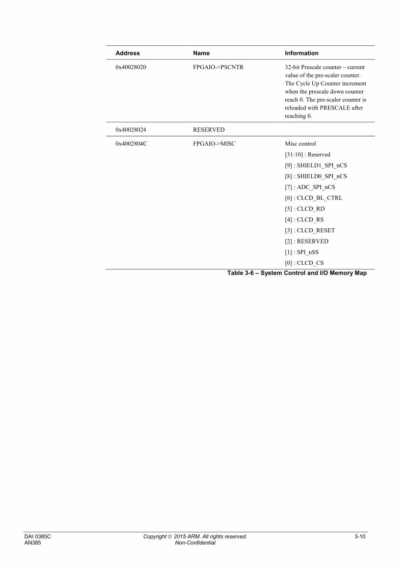
3.14 FPGA system control and I/O
The SMM implements an FPGA system control block.
Address Name Information
0x40028000 FPGAIO->LED0 LED connections
[31:2] : Reserved
[1:0] : LED
0x40028004 RESERVED
0x40028008 FPGAIO->BUTTON Buttons
[31:2] : Reserved
[1:0] : Buttons
0x4002800C RESERVED
0x40028010 FPGAIO->CLK1HZ 1Hz up counter
0x40028014 FPGAIO->CLK100HZ 100Hz up counter
0x40028018 FPGAIO->COUNTER Cycle Up Counter
Increments when 32-bit prescale
counter reach zero.
0x4002801C FPGAIO->PRESCALE Bit[31:0] – reload value for
prescale counter.
DAI 0385C Copyright 2015 ARM. All rights reserved. 3-10AN385 Non-Confidential
Address Name Information
0x40028020 FPGAIO->PSCNTR 32-bit Prescale counter – current
value of the pre-scaler counter.
The Cycle Up Counter increment
when the prescale down counter
reach 0. The pre-scaler counter is
reloaded with PRESCALE after
reaching 0.
0x40028024 RESERVED
0x4002804C FPGAIO->MISC Misc control
[31:10] : Reserved
[9] : SHIELD1_SPI_nCS
[8] : SHIELD0_SPI_nCS
[7] : ADC_SPI_nCS
[6] : CLCD_BL_CTRL
[5] : CLCD_RD
[4] : CLCD_RS
[3] : CLCD_RESET
[2] : RESERVED
[1] : SPI_nSS
[0] : CLCD_CS
Table 3-6 – System Control and I/O Memory Map
DAI 0385C Copyright 2015 ARM. All rights reserved. 4-1AN385 Non-Confidential
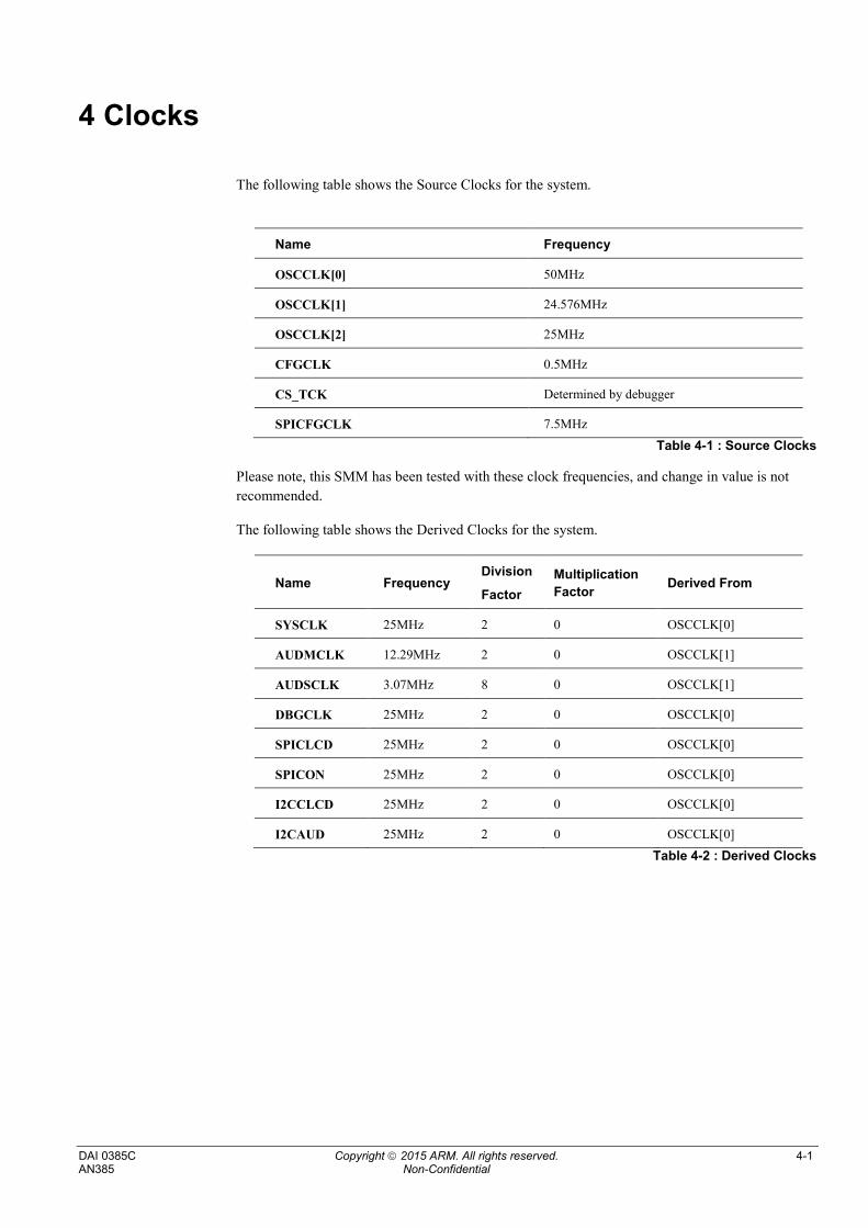
4 Clocks
The following table shows the Source Clocks for the system.
Name Frequency
OSCCLK[0] 50MHz
OSCCLK[1] 24.576MHz
OSCCLK[2] 25MHz
CFGCLK 0.5MHz
CS_TCK Determined by debugger
SPICFGCLK 7.5MHz
Table 4-1 : Source Clocks
Please note, this SMM has been tested with these clock frequencies, and change in value is not
recommended.
The following table shows the Derived Clocks for the system.
Name FrequencyDivision
Factor
Multiplication
FactorDerived From
SYSCLK 25MHz 2 0 OSCCLK[0]
AUDMCLK 12.29MHz 2 0 OSCCLK[1]
AUDSCLK 3.07MHz 8 0 OSCCLK[1]
DBGCLK 25MHz 2 0 OSCCLK[0]
SPICLCD 25MHz 2 0 OSCCLK[0]
SPICON 25MHz 2 0 OSCCLK[0]
I2CCLCD 25MHz 2 0 OSCCLK[0]
I2CAUD 25MHz 2 0 OSCCLK[0]
Table 4-2 : Derived Clocks
DAI 0385C Copyright 2015 ARM. All rights reserved. 5-1AN385 Non-Confidential
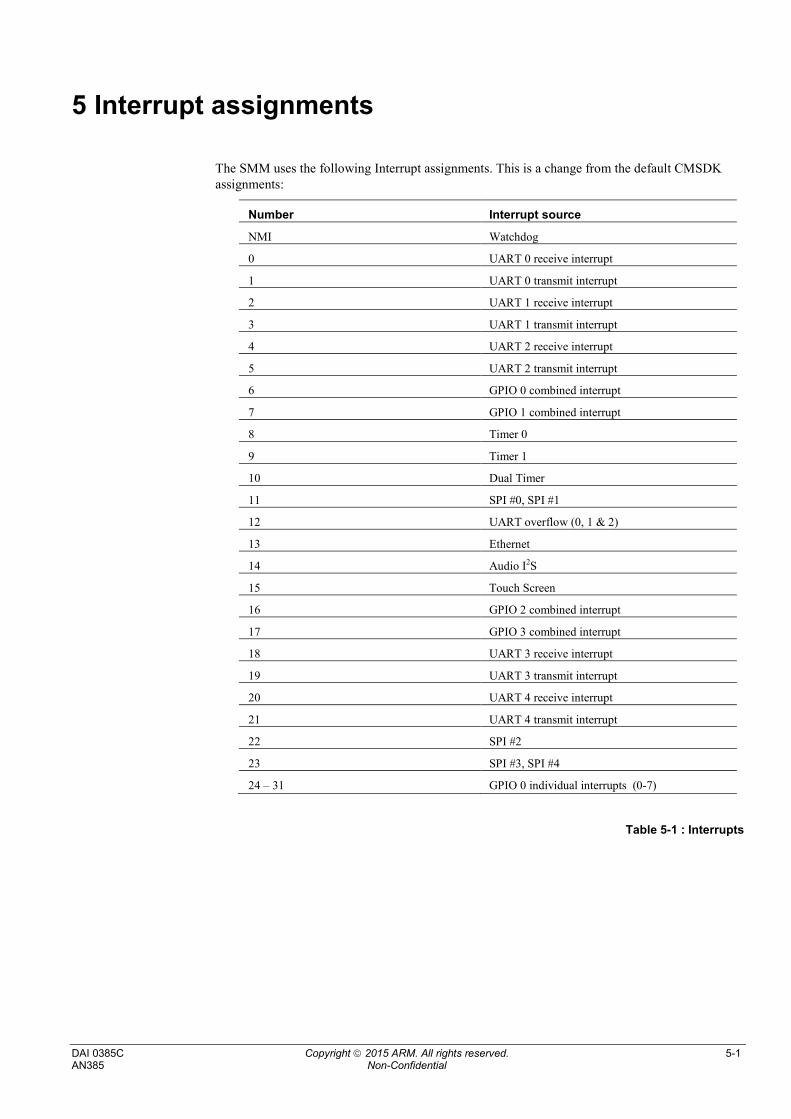
5 Interrupt assignments
The SMM uses the following Interrupt assignments. This is a change from the default CMSDKassignments:
Number Interrupt source
NMI Watchdog
0 UART 0 receive interrupt
1 UART 0 transmit interrupt
2 UART 1 receive interrupt
3 UART 1 transmit interrupt
4 UART 2 receive interrupt
5 UART 2 transmit interrupt
6 GPIO 0 combined interrupt
7 GPIO 1 combined interrupt
8 Timer 0
9 Timer 1
10 Dual Timer
11 SPI #0, SPI #1
12 UART overflow (0, 1 & 2)
13 Ethernet
14 Audio I2S
15 Touch Screen
16 GPIO 2 combined interrupt
17 GPIO 3 combined interrupt
18 UART 3 receive interrupt
19 UART 3 transmit interrupt
20 UART 4 receive interrupt
21 UART 4 transmit interrupt
22 SPI #2
23 SPI #3, SPI #4
24 – 31 GPIO 0 individual interrupts (0-7)
Table 5-1 : Interrupts
DAI 0385C Copyright 2015 ARM. All rights reserved. 6-1AN385 Non-Confidential
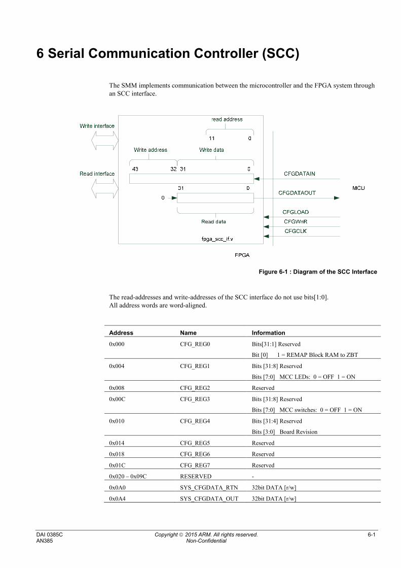
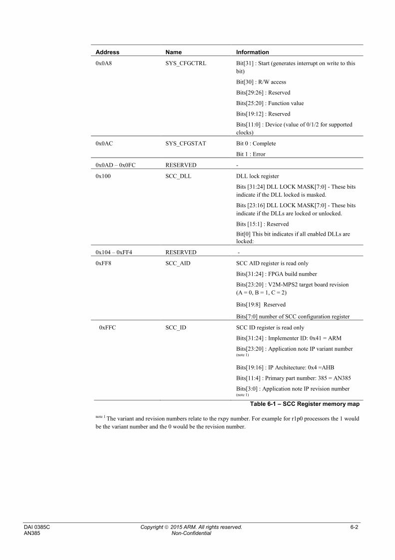
6 Serial Communication Controller (SCC)
The SMM implements communication between the microcontroller and the FPGA system throughan SCC interface.
Figure 6-1 : Diagram of the SCC Interface
The read-addresses and write-addresses of the SCC interface do not use bits[1:0].All address words are word-aligned.
Address Name Information
0x000 CFG_REG0 Bits[31:1] Reserved
Bit [0] 1 = REMAP Block RAM to ZBT
0x004 CFG_REG1 Bits [31:8] Reserved
Bits [7:0] MCC LEDs: 0 = OFF 1 = ON
0x008 CFG_REG2 Reserved
0x00C CFG_REG3 Bits [31:8] Reserved
Bits [7:0] MCC switches: 0 = OFF 1 = ON
0x010 CFG_REG4 Bits [31:4] Reserved
Bits [3:0] Board Revision
0x014 CFG_REG5 Reserved
0x018 CFG_REG6 Reserved
0x01C CFG_REG7 Reserved
0x020 – 0x09C RESERVED -
0x0A0 SYS_CFGDATA_RTN 32bit DATA [r/w]
0x0A4 SYS_CFGDATA_OUT 32bit DATA [r/w]
DAI 0385C Copyright 2015 ARM. All rights reserved. 6-2AN385 Non-Confidential
Address Name Information
0x0A8 SYS_CFGCTRL Bit[31] : Start (generates interrupt on write to this
bit)
Bit[30] : R/W access
Bits[29:26] : Reserved
Bits[25:20] : Function value
Bits[19:12] : Reserved
Bits[11:0] : Device (value of 0/1/2 for supported
clocks)
0x0AC SYS_CFGSTAT Bit 0 : Complete
Bit 1 : Error
0x0AD – 0x0FC RESERVED -
0x100 SCC_DLL DLL lock register
Bits [31:24] DLL LOCK MASK[7:0] - These bits
indicate if the DLL locked is masked.
Bits [23:16] DLL LOCK MASK[7:0] - These bits
indicate if the DLLs are locked or unlocked.
Bits [15:1] : Reserved
Bit[0] This bit indicates if all enabled DLLs arelocked:
0x104 – 0xFF4 RESERVED -
0xFF8 SCC_AID SCC AID register is read only
Bits[31:24] : FPGA build number
Bits[23:20] : V2M-MPS2 target board revision
(A = 0, B = 1, C = 2)
Bits[19:8] Reserved
Bits[7:0] number of SCC configuration register
0xFFC SCC_ID SCC ID register is read only
Bits[31:24] : Implementer ID: 0x41 = ARM
Bits[23:20] : Application note IP variant number(note 1)
Bits[19:16] : IP Architecture: 0x4 =AHB
Bits[11:4] : Primary part number: 385 = AN385
Bits[3:0] : Application note IP revision number(note 1)
Table 6-1 – SCC Register memory map
note 1 The variant and revision numbers relate to the rxpy number. For example for r1p0 processors the 1 would
be the variant number and the 0 would be the revision number.
DAI 0385C Copyright 2015 ARM. All rights reserved. 7-3AN385 Non-Confidential
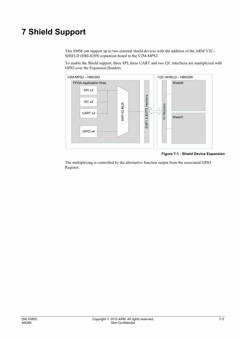
7 Shield Support
This SMM can support up to two external shield devices with the addition of the ARM V2C-SHIELD (HBI-0289) expansion board to the V2M-MPS2.
To enable the Shield support, three SPI, three UART and two I2C interfaces are multiplexed withGPIO over the Expansion Headers.
khioj
GPIO x4
UART x3
SPI x3
I2C x2
V2M-MPS2 – HBI0263
FPGA Application Note
V2C-SHIELD – HBI0289
Shield0
Shield1
Figure 7-1 : Shield Device Expansion
The multiplexing is controlled by the alternative function output from the associated GPIORegister.
DAI 0385C Copyright 2015 ARM. All rights reserved. 7-4AN385 Non-Confidential
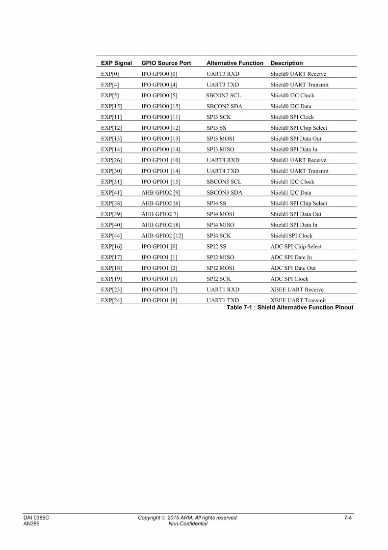
EXP Signal GPIO Source Port Alternative Function Description
EXP[0] IPO GPIO0 [0] UART3 RXD Shield0 UART Receive
EXP[4] IPO GPIO0 [4] UART3 TXD Shield0 UART Transmit
EXP[5] IPO GPIO0 [5] SBCON2 SCL Shield0 I2C Clock
EXP[15] IPO GPIO0 [15] SBCON2 SDA Shield0 I2C Data
EXP[11] IPO GPIO0 [11] SPI3 SCK Shield0 SPI Clock
EXP[12] IPO GPIO0 [12] SPI3 SS Shield0 SPI Chip Select
EXP[13] IPO GPIO0 [13] SPI3 MOSI Shield0 SPI Data Out
EXP[14] IPO GPIO0 [14] SPI3 MISO Shield0 SPI Data In
EXP[26] IPO GPIO1 [10] UART4 RXD Shield1 UART Receive
EXP[30] IPO GPIO1 [14] UART4 TXD Shield1 UART Transmit
EXP[31] IPO GPIO1 [15] SBCON3 SCL Shield1 I2C Clock
EXP[41] AHB GPIO2 [9] SBCON3 SDA Shield1 I2C Data
EXP[38] AHB GPIO2 [6] SPI4 SS Shield1 SPI Chip Select
EXP[39] AHB GPIO2 7] SPI4 MOSI Shield1 SPI Data Out
EXP[40] AHB GPIO2 [8] SPI4 MISO Shield1 SPI Data In
EXP[44] AHB GPIO2 [12] SPI4 SCK Shield1SPI Clock
EXP[16] IPO GPIO1 [0] SPI2 SS ADC SPI Chip Select
EXP[17] IPO GPIO1 [1] SPI2 MISO ADC SPI Date In
EXP[18] IPO GPIO1 [2] SPI2 MOSI ADC SPI Date Out
EXP[19] IPO GPIO1 [3] SPI2 SCK ADC SPI Clock
EXP[23] IPO GPIO1 [7] UART1 RXD XBEE UART Receive
EXP[24] IPO GPIO1 [8] UART1 TXD XBEE UART TransmitTable 7-1 : Shield Alternative Function Pinout


![Introduction - cvgmt: homecvgmt.sns.it/media/doc/paper/3180/Sobolev@Stability@final.pdf · for some v2M. As a consequence of Theorem 1.1 and the main result of [10] (see Theorem 5.5](https://img.pdfslide.us/doc/110x75/5ffdf0b067c3b935d03aaa09/introduction-cvgmt-stabilityfinalpdf-for-some-v2m-as-a-consequence-of-theorem.jpg)