Embed Size (px)
Citation preview

www.irf.com 1AN-118511-Nov-15
Application Note AN-1185
A guide to the SBP5AS: A Radiation hardened DCto DC converter module
By Paul L. Schimel PE and Truls M. Andersen
IntroductionThis Application Note should serve as a map for the use and application of the SBP
converter module. It contains all of the critical parameters associated with each pin and someguidance as to how to set them up in the circuit.
Basic TopologyThe SBP DC to DC converter is comprised of a voltage-mode control IC. Direct
paralleling is not possible.The converter is a synchronous buck converter capable of starting into a pre-bias
condition. This is accomplished by a diode emulation mode built into the integrated controller thatis active only during the startup condition. When a pre-bias startup condition is sensed, thecontroller turns off the lowside MOSFET thereby allowing the body diode of the device to blockthat current and not pull down the output voltage. Diode Emulation mode is not used at light,steady state loads in the SBP DC to DC converter in order to maintain the best possible transientresponse.

www.irf.com 2AN-118511-Nov-15
Figure 1.) SBP block diagram
Output Adjust Pin:The output voltage of the converter is settable between 0.8 and 3.3V. The resistor that
sets this voltage, RAdjust can be calculated by one of two equations depending on whether or notremote sense is tied to the load or to the module output:With Remote Sense pin tied directly to converter output:
121025.026-Vout*31.600
191.686−=AdjustR
With Remote Sense pin tied to the load:
121024.960-Vout*31.600
189.600−=AdjustR
If a final trim is used on the end equipment, RAdjust should be calculated from 1.035*Vout(output voltage is initially set 3.5% higher).
Note: For static load, output voltage can be 85% of the input voltage.For high load current variations the output voltage shall be limited to 75% of the input voltage.This is to obtain the dynamic performance without saturating the internal PWM controller.
www.irf.com 3AN-118511-Nov-15
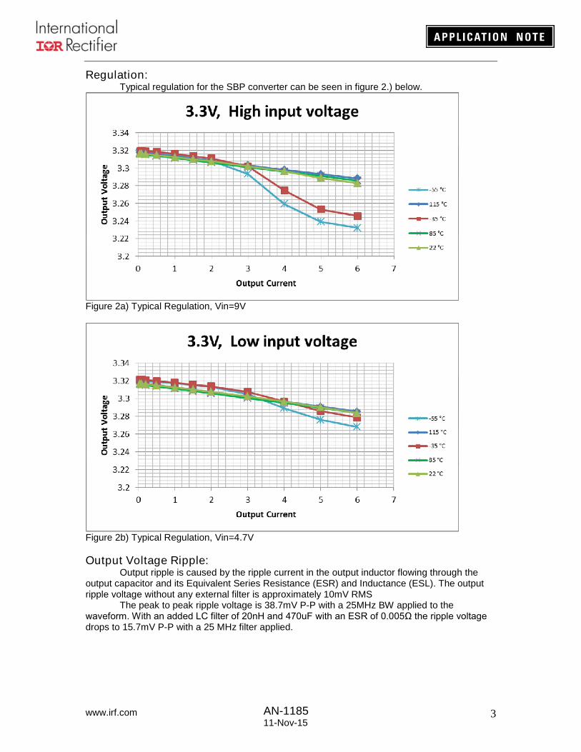
Regulation:Typical regulation for the SBP converter can be seen in figure 2.) below.
Figure 2a) Typical Regulation, Vin=9V
Figure 2b) Typical Regulation, Vin=4.7V
Output Voltage Ripple:Output ripple is caused by the ripple current in the output inductor flowing through the
output capacitor and its Equivalent Series Resistance (ESR) and Inductance (ESL). The outputripple voltage without any external filter is approximately 10mV RMS
The peak to peak ripple voltage is 38.7mV P-P with a 25MHz BW applied to thewaveform. With an added LC filter of 20nH and 470uF with an ESR of 0.005Ω the ripple voltage drops to 15.7mV P-P with a 25 MHz filter applied.

www.irf.com 4AN-118511-Nov-15
Figure 3.) Output ripple with no external filter
Figure 4.) Output ripple with 20nH and 470uF, 0.005Ω external filter

www.irf.com 5AN-118511-Nov-15
Internal and External Compensation:In terms of compensation, the internal inductor and capacitor contribute a double pole at
roughly 5.63 kHz. The internal output capacitor has a zero at roughly 67.7 kHz. The erroramplifier is compensated in a Type III compensation scheme with dominant poles at 0Hz and 225kHz and zeros at roughly 0.5 kHz and 6.8 kHz. Combined with the gain of the internal erroramplifier, this combination offers a 0dB crossover frequency of approximately 40 kHz. At thiscrossover frequency, the converter has between 70 and 90 degrees of phase margin dependingon line, load and output voltage conditions.
The SBP DC to DC converter was designed with the unique ability to not only addoptional capacitance to the converter and have it remain stable, but to add an additional lowfrequency gain to the converter and further improve the transient response with the added outputcapacitance. While the internal output capacitance in the SBP converter is sufficient for mostapplications, there are clearly instances where a lot of local capacitance is needed for locallybypassing high transient loads.
To compensate for additional output capacitance, a small external capacitor can beconnected between the Sense and Output Adjust pins that will place an additional zero at lowfrequency and raise the gain of the control loop slightly to compensate for additional added outputcapacitance. The calculation of this added capacitance is included under the SENSE PINheading.
Sense PinThe SENSE PIN can be used to reduce the drop in the positive conductor that connects
the converter to the load. In applications with a positive conductor longer than a few inches orcontributing more than 1% I*R drop at maximum current, the sense pin should be connected asclose to the load as possible. In applications with minimal conductor drop the sense pin should beconnected to the output of the converter or it can be simply left open. The sense pin should NOTbe shorted to return on the POL converter..
The compensation of the converter is designed for minimal perturbation by addedparasitic components. However when filter capacitance is added to the output the loopperformance can be improved slightly by the use of C adjust (Cadj), as described below. Theaddition of this component from the SENSE to the ADJUST pin adds a low frequency zero to thecontrol loop offering slightly more gain in the feedback loop.
The maximum value of Cadj is determined by the external capacitance compared withthe internal capacitance, and the external ESR compared with the internal ESR.
Ω≤≤
≤
m
ESRkand
uF
Ck
k
nFC
outout
adj
5470
5.1

www.irf.com 6AN-118511-Nov-15
Rhys
Rpgood
Vpgood
Rsot2
37k
Stray in wire Stray in wire
Vsupply Vout
Power good
Cout
U2
SBI-POL
Vin1
GND12
Enable3
Track4
Pgood5
Adjust6
Remote sense7
Sy nc8
GND29
Vout10
Lout
Radju
st
1k1
Rsto
p
Lin
C210
Cadj
Figure 5.) Added output capacitor diagram
Load step performanceThe Lout (40nH and 0.0056Ω) of stray series inductance and DCR showed 32mV in voltage deviation on the filter output Cout (470uF and 0.005Ω) . This corresponds to 10.6mΩ in output impedance. Cadj is 1.5nF.
Figure 6.) 3A load step, 1: V external filter, 2: V SBP output
Input Voltage HysteresisThe input voltage hysteresis can be adjusted by and resistor placed from the Vin
to Enable.The resistor value can be found:
hys
hys
hysV
VkR
⋅−
⋅Ω=
796.11
33.83
Where Vhys is the desired input voltage hysteresis.The hysteresis is 0.557V with Rhys open circuit. Vhys can only be lowered by adding
finite value of Rhys.
Input Start/Stop VoltageA resistor connected from the ENABLE to GND sets the UVLO turn-off threshold voltage.
The resistor value can be found by:
hysstop
hys
stopVVV
kVR
⋅−−
⋅=
06.66.0
50
The UVLO turn-on threshold voltage is the UVLO turn-off threshold voltage plus the hysteresis
hysstopstart VVV +=
The minimum UVLO turn-off threshold voltage is 3V

www.irf.com 7AN-118511-Nov-15
Input ripple currentThe POL converter is designed to accommodate a wide variety of input conductors and wireharnesses for maximum design flexibility
Calculation of the input ripple current is shown with an inductive harness.The input ripple current is the Thevenin voltage (22mVrms) divided by the harness impedance atthe switching frequency. This gives the following with a 100nH to 2.5uH variation:
68 mArms which is 97dBuA for 100nH14 mArms which is 83dBuA for 500nH3 mArms which is 69dBuA for 2500nH
Sync Pin
Several POL converters can be connected to the same input supply. If several inputs areconnected to an inductive source, mixing of the different switching frequencies will occur, creatinga very low sub harmonic ripple on the output.
This can be prevented by adding a small inductance in series with the inputs and acapacitor in the common point. Further, one should pay close attention to resonances in the inputwiring harness and capacitors.
Another way to prevent the intermodulation is to synchronize the converter to a commonclock. This is accomplished by driving the SYNC PIN from an external clock. The synchronizationfrequency range is 425 KHz to 575 KHz. The synchronization signal source must be able tosource the current of 1.0mA with the voltage level of minimum 2.0V at high and maximum 0.8V atlow. The rise and fall times of the synchronizing waveform should be 0.2us or less respectively.
Parallel Enables
The Enable inputs of several SBPs can be paralleled. This can be done directly if thereare no requirements for timing between the outputs. The only difference is that the Rstart / Rstopresistance is divided by 2 (number of paralleled SBPs).
Alternatively, timing can be altered by adding some resistance between the ENABLE pinsand the combined Rstop resistor. This is done to stop the controlling converter first, to insuretiming.
Soft start
The Soft start period can be modified by adding a capacitor from the TRACK pin to GND.The internal and external output capacitance needs to be charged during the soft start event. Thischarge current is added to the load current during start up, and the sum needs to be within themaximum current rating.
nFtnFC
I
VCCt
ssext
ech
outextoutout
ss
82*39
)(
arg
,int,
−=
⋅+=
tss is the soft start time in [ms].
The internal capacitance is 470uF.

www.irf.com 8AN-118511-Nov-15
Power Good Pin to Sequence Multiple SBP modules
Tracking is important in applications with different processor and or I/O voltages. Themanufacturers will often recommend a startup sequence in these cases to mitigate any datacontention. For repeatable operation, it is preferable to use the POWER GOOD pin as outlinedbelow.
To rely on the Soft Start capacitance for tracking is not a recommended design practice.This is due to the tolerance of the soft start capacitor combined with the tolerance in the soft startcircuit in the PWM controller in the SBP. The combination of these tolerances can result in worsethan expected tracking performance.
Sequence Type: Vout1 before Vout2
Power good 2
Vin2
Vout1
Vout2
Vlab
Power good 1
R2
04
1k
96
L201
110n
R2
05
1k
96
C203470UESR = 5m
T5
30
R2
01
10k
U2
SBI-POL
Vin1
GND12
Enable3
Track4
Pgood5
Adjust6
Remote sense7
Sy nc8
GND29
Vout10
C204470UESR = 5m
T5
30
L203
15n
L202
1u
C202220UESR = 35m
T5
10
R2
02
1k
21
R2
00
8k
25
R2
03
13
k7
L200
110n
U3
SBI-POL
Vin1
GND12
Enable3
Track4
Pgood5
Adjust6
Remote sense7
Sy nc8
GND29
Vout10
L204
15n
Figure 7.) One Output After the Other Diagram
The power good pin of the first output is connected to the enable of the second output.The second output will start to rise when the first output releases the power good, whichapproximately is 1.5 times the Soft start time. R200 controls the start/stop voltage, where R201 ismore of a protection at very low input voltages (if converter 1 stops functioning before converter 2– below 3V)

www.irf.com 9AN-118511-Nov-15
Sequence type: Ratiometric Tracking
Ratiometric tracking is when the outputs have the same percentage of their final outputvoltage during turn ON. Ratiometric tracking can be accomplished by connecting a voltage dividerfrom the highest output voltage to the soft start pin of the lowest output voltage. The voltagedivider shall be 0.6V / Vout1. The low side of the voltage divider must be connected to the powergood of output 1.
Rhy
s1
Ruv
p
Rs
top
1
Rp
go
od
1
Rpg
oo
d2
Power good 2
R21
1
121
k
R2
12
12
1k
Vin2 Vout2
Vout1
Vout1
Power good 1
Vlab
U2
SBI-POL
Vin1
GND12
Enable3
Track4
Pgood5
Adjust6
Remote sense7
Sy nc8
GND29
Vout10
Css1
Cout1Cin1
Css2
Lin opt2
110n
L203
15n
L204
15n
R206
1k33
Lin opt1
110n
R20
4
1k
1
R2
05
12
k1
Cout2
U3
SBI-POL
Vin1
GND12
Enable3
Track4
Pgood5
Adjust6
Remote sense7
Sy nc8
GND29
Vout10
R207
6k19
Lin1
1u
Stray in wire
Stray in wire
Stray in wire
Figure 8.) Ratiometric Tracking Diagram
Vref is 0.6V.
207
1
206
1207 5.01
RVV
VR
kkV
VR
refout
ref
ref
out
⋅−
=
+⋅=

www.irf.com 10AN-118511-Nov-15
Sequencing Type: Simultaneous tracking
Simultaneous tracking is when the output voltages rise at the same actual level. This canbe accomplished by connecting a voltage divider from the highest output voltage to the soft startpin of the lowest output voltage.
The voltage divider shall be 0.6V / Vout2
Stray in wire
Lin1
Rhy
s1
Rs
top
1
Lout1
15n
Stray in wire
Stray in wire
Lout2
15n
Vin2
Cout1
Vout1
Cout2
Vout1
Vout2
Vsupply
Power good 1
Cin1
R206
3k16
Rp
go
od
1
Ruv
p
Rs
ot1
237
k
Ra
dju
st1
1k
1
R207
2k37
U3
SBI-POL
Vin1
GND12
Enable3
Track4
Pgood5
Adjust6
Remote sense7
Sy nc8
GND29
Vout10
Css1
U2
SBI-POL
Vin1
GND12
Enable3
Track4
Pgood5
Adjust6
Remote sense7
Sy nc8
GND29
Vout10
Rso
t2
16
2k
Rad
jus
t2
12
k1
Css2
Lin opt1
110n
Lin opt2
110n
Rpg
oo
d2
Power good 2
Figure 9.) Simultaneous Tracking Diagram
207
2
206
207
2
21
2207 5.01
RVVV
VVR
RIV
VVV
kkV
VR
outrefout
outref
ss
out
outoutout
ref
out
⋅∆−−
∆+=
⋅⋅−
=∆
+⋅=
Vref is 0.6V. Iss is 23uA.

www.irf.com 11AN-118511-Nov-15
Efficiency
The measured data below shows the efficiency of the POL converter under best andworst case conditions. The efficiency curves are taken at -55, 22 and 115°C.
Figure 10.) Efficiency vs. Load Current for Vin=4.7V, Vout=3.3V
Figure 11.) Efficiency vs. Load Current for Vin=7V, Vout=1.2V
Discussion of Losses:
Internal Switches:
The temperature plots illustrate the Rdson dependency of the MOSFETs in the regulatorIC. At lower temperatures, the Rdson of the MOSFETs is appreciably lower than at highertemperatures. At higher temperatures, the charge and discharge currents to the output inductorcause more losses in the respective high and low side switches as a result of this higherresistance.

www.irf.com 12AN-118511-Nov-15
Assuming fixed input voltage, the lower voltage output requires a proportionally lowerduty cycle on the high side switch. This means that the lowside switch is on for a proportionallylonger duration and the freewheel currents cause more losses in this switch.
As the input voltage is raised, this condition gets worse in two ways. The lowside switchis clearly on for a longer duration with rising input voltage and the switching losses in the highside switch are exponentially greater as they are associated with the various CV2/2 energies inthe switch capacitances.
Output inductor:
At narrow duty cycles (thereby lower output voltages), the AC losses in the outputinductor are much worse than at larger duty cycles. This is due to the higher frequency energyassociated with the narrow pulse causing additional eddy current losses in the core material andcopper windings. The core material was chosen with this in mind as well as the ruggedapplications, temperature ranges and environments that the inductor will see.
Input and Output Capacitor
The primary loss mechanism in the capacitors stems from the RMS value of the AC ripplecurrent flowing through the ESR of the capacitors. These losses are minimal in the SBP module.
PCB traces
The losses in the PCB traces are fairly straightforward. At 500 KHz the depth ofpenetration in copper is approximately 0.0042” or 4.2 mils. The copper on the PCB is slightlythinner than this so any additional AC losses beyond the I*R drop in a given trace is minimal. ThePCB was well routed with plenty of cross section in the power path conductors to keep the DClosses to a minimum.
Thermal Plot
The thermal plot shows the hot spots in the module. The control IC is mounted on the topof the PCB with the output inductor mounted under the control IC on the bottom of the PCB.These are the major heat sources in the SBP module. The module is contained in an Aluminumhousing assembled over the top and bottom of the PCB which helps conduct heat away from thecontrol IC. The ambient temperature for the plot is 20°C.
Figure 12.) Module drawing

www.irf.com 13AN-118511-Nov-15
Figure 13.) FEA based simulation of module thermals
Mounting
The POL must be mounted to a thermally conductive plate or chassis with four screws.Proposed screw size is M2 or UNC 1-72 and 12 mm (0.47") in length. A recommended torque is0.25nm (35Ozln). The host chassis should be mechanically rigid and thermally conductiveenough to support the mass and power loss. Typical power loss at full load is 3.5W, but can besmaller at a lighter load.
Wiring
The positive and negative conductors into and out of the module should have a crosssection of at least 2500 circular mils. If Wire is to be used, use 16AWG or larger cross sectionwire. Twisted pair is strongly recommended.
Conclusion
This document should serve as an application resource for the use of the SBP POLConverter. We have tried to address every aspect of the application of the POL converter as wellas the use of combined POL converters. Please refer to the datasheet for specific values anddimensions that may not be covered herein.