Embed Size (px)
Citation preview

As originally published in the IPC APEX EXPO Proceedings.
Application Methods and Thermal Mechanical Reliability of Polymeric
Solder Joint Encapsulation Materials (SJEM) on SnAgCu Solder Joints
Jagadeesh Radhakrishnan1, Sunny Lu2, Al Molina1,Olivia H. Chen3, Wu Jin Chang2, Xin
Wang2, Kok Kwan Tang4, Scott Mokler5, and Raiyo Aspandiar5
1Intel Corporation, Folsom, CA, USA 2Quanta Shanghai, China
3Formerly at Intel Corporation, Folsom CA,USA 4Intel Corporation, Kulim, Malaysia
5Intel Corporation, Hillsboro, OR, USA
Abstract
With each new generation, the complexity in the design of flip chip devices, as exemplified by thinner package stack-ups,
larger device sizes, and multiple die configurations, is increasing significantly. This is creating new challenges in their
surface mount manufacturing and their solder joint reliability. To improve surface mount solder joint reliability under
mechanical stresses, such as those imposed under shock, drop, and vibration during transportation and end user handling, the
use of polymeric materials to provide added reinforcement to the second level solder interconnects on flip chip ball grid
arrays (FCBGA)and package-on-package (POP) solder joints has been proposed as a solution. Some of the common
examples of such polymeric reinforcement applications in manufacturing include, but are not limited to, corner glue edge
bonding, underfill (UF) application, and epoxy-containing solder pastes. However, as the solder joints’ pitch size and height
decreases, control of the extent and uniformity of polymeric encapsulation of second level solder joints becomes more
challenging. As a result, solder joint encapsulation materials (SJEM) have been developed to provide a better controlled and
localized application process. Unlike other polymeric materials in use today, these SJEMs do not require an additional step
for cure, since they are applied before the reflow soldering process step and cure during the reflow soldering process step.
Based on past studies on polymer reinforced solder joints, mechanical shock performance generally improved with the
application of the polymer reinforcement and was less sensitive to the polymeric material properties as long as the material
has acceptable application, curing, adhesion and fracture strength properties. However, thermal cycling reliability is more
sensitive to certain material properties of the reinforcing polymer. The glass transition temperature (Tg) and the coefficient of
thermal expansion (CTE) are two such properties [1-2]. Materials with a low Tg and a high CTE often lead to accelerated
solder joint failure from thermal fatigue. Therefore, the material properties of SJEM and the extent of material coverage on
the solder joint both play important roles in optimizing solder joint reliability performance under mechanical and thermal
conditions.
In this paper, two SJEM material application methods, dispensing and dipping, will be studied for the extent and uniformity of
their encapsulation of high density BGA solder joints. The solder joint mechanical shock and thermal cycling reliability
from these two SJEM dispensing techniques, which correspond to different encapsulation coverage, will also be analyzed and
discussed.
From the assembly and reliability test results, both SJEM materials showed process feasibility to be applied, reflowed, and
cured with SAC305 solder paste. Both SJEM application methods showed promising mechanical shock and temperature
cycle reliability. These materials can be considered as a solution to replace underfills and corner glues for smaller, finer pitch
components in the future.
Introduction
Area Array components, particularly those for microprocessors, memory and chip sets, are in a continuous miniaturization
trend [3,4]. As an example, the physical volume of the company microprocessor Flip Chip Ball Grid Array (FCBGA)
packages have reduced from 1440 cm3 for the device generation introduced in 2010 to 330 cm3 for the device generation
introduced in 2015. Also, the z heights of these packages have decreased in half from 2 mm for the device generation in 2010
to 1 mm for the device generation in 2015 [5]. The decrease in the size of such area array components, as Ball Grid Arrays
(BGA), Chip Scale Packages (CSP), and Wafer Level Packages (WLP), concomitantly decreases the size of their solder
joints and thereby drives the need to enhance their robustness when exposed to mechanical stresses experienced under
vibration and shock impact, as well as thermomechanical stresses experienced under temperature and power cycling
[6].Additionally, the field use temperatures of these solders are very high on their homologous temperatures scale[7]. Hence,
polymeric reinforcement of area array solder joints become a necessity to lower the risk for solder joint failure in the field.
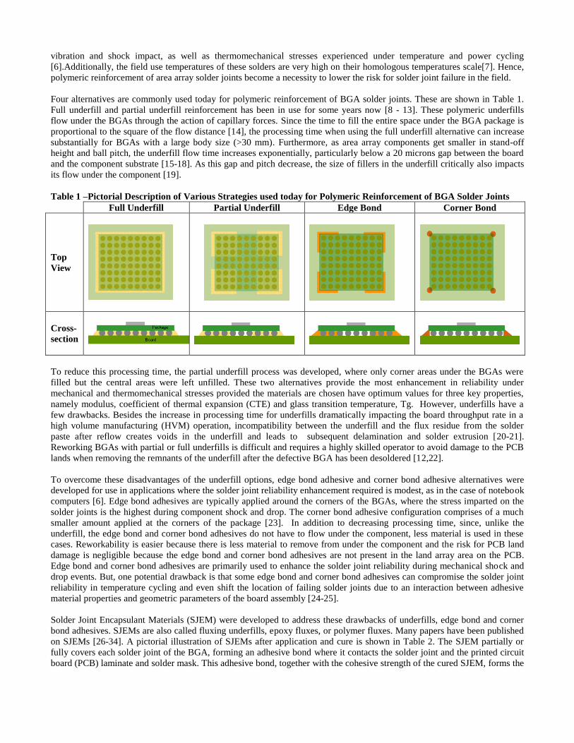
Four alternatives are commonly used today for polymeric reinforcement of BGA solder joints. These are shown in Table 1.
Full underfill and partial underfill reinforcement has been in use for some years now [8 - 13]. These polymeric underfills
flow under the BGAs through the action of capillary forces. Since the time to fill the entire space under the BGA package is
proportional to the square of the flow distance [14], the processing time when using the full underfill alternative can increase
substantially for BGAs with a large body size (>30 mm). Furthermore, as area array components get smaller in stand-off
height and ball pitch, the underfill flow time increases exponentially, particularly below a 20 microns gap between the board
and the component substrate [15-18]. As this gap and pitch decrease, the size of fillers in the underfill critically also impacts
its flow under the component [19].
Table 1 –Pictorial Description of Various Strategies used today for Polymeric Reinforcement of BGA Solder Joints
Full Underfill Partial Underfill Edge Bond Corner Bond
Top
View
Cross-
section
To reduce this processing time, the partial underfill process was developed, where only corner areas under the BGAs were
filled but the central areas were left unfilled. These two alternatives provide the most enhancement in reliability under
mechanical and thermomechanical stresses provided the materials are chosen have optimum values for three key properties,
namely modulus, coefficient of thermal expansion (CTE) and glass transition temperature, Tg. However, underfills have a
few drawbacks. Besides the increase in processing time for underfills dramatically impacting the board throughput rate in a
high volume manufacturing (HVM) operation, incompatibility between the underfill and the flux residue from the solder
paste after reflow creates voids in the underfill and leads to subsequent delamination and solder extrusion [20-21].
Reworking BGAs with partial or full underfills is difficult and requires a highly skilled operator to avoid damage to the PCB
lands when removing the remnants of the underfill after the defective BGA has been desoldered [12,22].
To overcome these disadvantages of the underfill options, edge bond adhesive and corner bond adhesive alternatives were
developed for use in applications where the solder joint reliability enhancement required is modest, as in the case of notebook
computers [6]. Edge bond adhesives are typically applied around the corners of the BGAs, where the stress imparted on the
solder joints is the highest during component shock and drop. The corner bond adhesive configuration comprises of a much
smaller amount applied at the corners of the package [23]. In addition to decreasing processing time, since, unlike the
underfill, the edge bond and corner bond adhesives do not have to flow under the component, less material is used in these
cases. Reworkability is easier because there is less material to remove from under the component and the risk for PCB land
damage is negligible because the edge bond and corner bond adhesives are not present in the land array area on the PCB.
Edge bond and corner bond adhesives are primarily used to enhance the solder joint reliability during mechanical shock and
drop events. But, one potential drawback is that some edge bond and corner bond adhesives can compromise the solder joint
reliability in temperature cycling and even shift the location of failing solder joints due to an interaction between adhesive
material properties and geometric parameters of the board assembly [24-25].
Solder Joint Encapsulant Materials (SJEM) were developed to address these drawbacks of underfills, edge bond and corner
bond adhesives. SJEMs are also called fluxing underfills, epoxy fluxes, or polymer fluxes. Many papers have been published
on SJEMs [26-34]. A pictorial illustration of SJEMs after application and cure is shown in Table 2. The SJEM partially or
fully covers each solder joint of the BGA, forming an adhesive bond where it contacts the solder joint and the printed circuit
board (PCB) laminate and solder mask. This adhesive bond, together with the cohesive strength of the cured SJEM, forms the
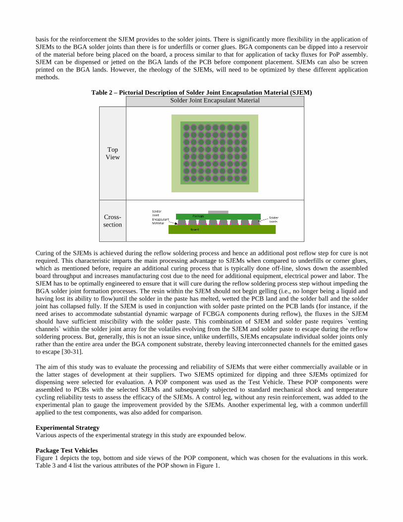
basis for the reinforcement the SJEM provides to the solder joints. There is significantly more flexibility in the application of
SJEMs to the BGA solder joints than there is for underfills or corner glues. BGA components can be dipped into a reservoir
of the material before being placed on the board, a process similar to that for application of tacky fluxes for PoP assembly.
SJEM can be dispensed or jetted on the BGA lands of the PCB before component placement. SJEMs can also be screen
printed on the BGA lands. However, the rheology of the SJEMs, will need to be optimized by these different application
methods.
Table 2 – Pictorial Description of Solder Joint Encapsulation Material (SJEM)
Solder Joint Encapsulant Material
Top
View
Cross-
section
Curing of the SJEMs is achieved during the reflow soldering process and hence an additional post reflow step for cure is not
required. This characteristic imparts the main processing advantage to SJEMs when compared to underfills or corner glues,
which as mentioned before, require an additional curing process that is typically done off-line, slows down the assembled
board throughput and increases manufacturing cost due to the need for additional equipment, electrical power and labor. The
SJEM has to be optimally engineered to ensure that it will cure during the reflow soldering process step without impeding the
BGA solder joint formation processes. The resin within the SJEM should not begin gelling (i.e., no longer being a liquid and
having lost its ability to flow)until the solder in the paste has melted, wetted the PCB land and the solder ball and the solder
joint has collapsed fully. If the SJEM is used in conjunction with solder paste printed on the PCB lands (for instance, if the
need arises to accommodate substantial dynamic warpage of FCBGA components during reflow), the fluxes in the SJEM
should have sufficient miscibility with the solder paste. This combination of SJEM and solder paste requires `venting
channels` within the solder joint array for the volatiles evolving from the SJEM and solder paste to escape during the reflow
soldering process. But, generally, this is not an issue since, unlike underfills, SJEMs encapsulate individual solder joints only
rather than the entire area under the BGA component substrate, thereby leaving interconnected channels for the emitted gases
to escape [30-31].
The aim of this study was to evaluate the processing and reliability of SJEMs that were either commercially available or in
the latter stages of development at their suppliers. Two SJEMS optimized for dipping and three SJEMs optimized for
dispensing were selected for evaluation. A POP component was used as the Test Vehicle. These POP components were
assembled to PCBs with the selected SJEMs and subsequently subjected to standard mechanical shock and temperature
cycling reliability tests to assess the efficacy of the SJEMs. A control leg, without any resin reinforcement, was added to the
experimental plan to gauge the improvement provided by the SJEMs. Another experimental leg, with a common underfill
applied to the test components, was also added for comparison.
Experimental Strategy
Various aspects of the experimental strategy in this study are expounded below.
Package Test Vehicles Figure 1 depicts the top, bottom and side views of the POP component, which was chosen for the evaluations in this work.
Table 3 and 4 list the various attributes of the POP shown in Figure 1.
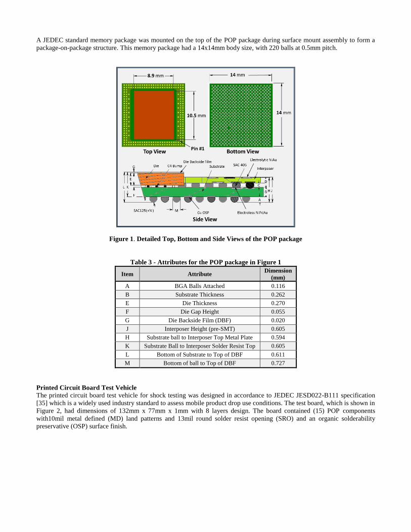
A JEDEC standard memory package was mounted on the top of the POP package during surface mount assembly to form a
package-on-package structure. This memory package had a 14x14mm body size, with 220 balls at 0.5mm pitch.
Figure 1. Detailed Top, Bottom and Side Views of the POP package
Table 3 - Attributes for the POP package in Figure 1
Item Attribute Dimension
(mm)
A BGA Balls Attached 0.116
B Substrate Thickness 0.262
E Die Thickness 0.270
F Die Gap Height 0.055
G Die Backside Film (DBF) 0.020
J Interposer Height (pre-SMT) 0.605
H Substrate ball to Interposer Top Metal Plate 0.594
K Substrate Ball to Interposer Solder Resist Top 0.605
L Bottom of Substrate to Top of DBF 0.611
M Bottom of ball to Top of DBF 0.727
Printed Circuit Board Test Vehicle
The printed circuit board test vehicle for shock testing was designed in accordance to JEDEC JESD022-B111 specification
[35] which is a widely used industry standard to assess mobile product drop use conditions. The test board, which is shown in
Figure 2, had dimensions of 132mm x 77mm x 1mm with 8 layers design. The board contained (15) POP components
with10mil metal defined (MD) land patterns and 13mil round solder resist opening (SRO) and an organic solderability
preservative (OSP) surface finish.
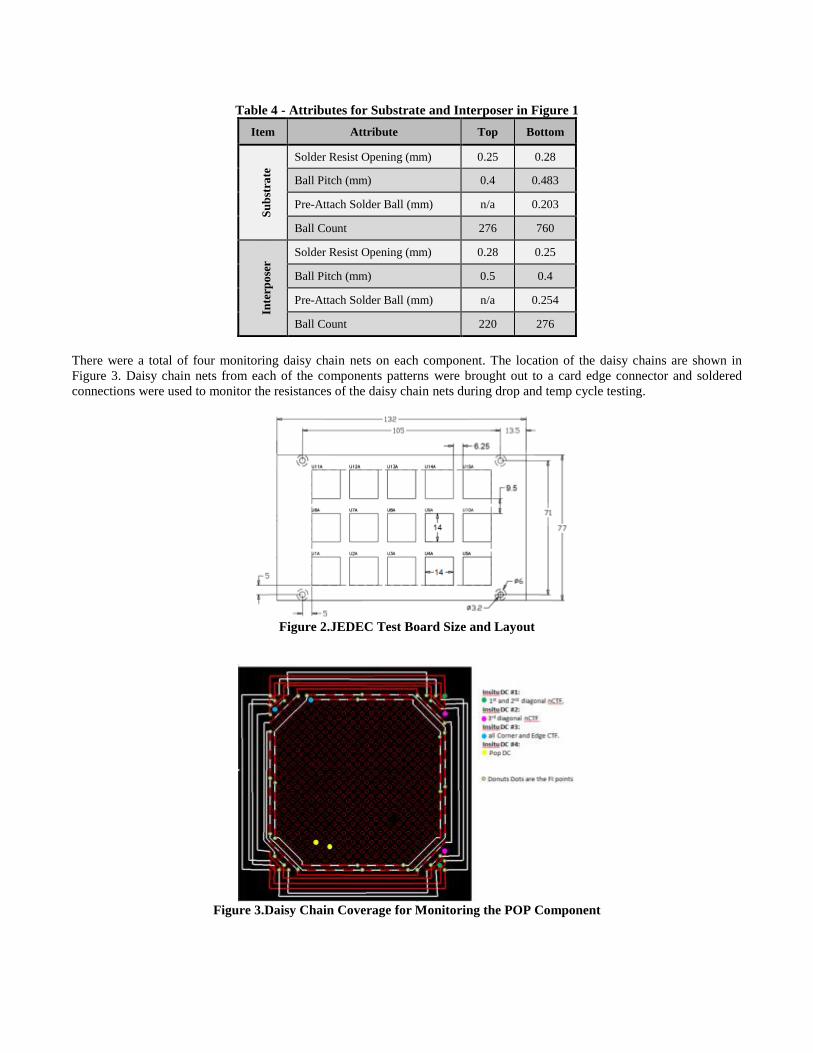
Table 4 - Attributes for Substrate and Interposer in Figure 1
Item Attribute Top Bottom
Su
bst
rate
Solder Resist Opening (mm) 0.25 0.28
Ball Pitch (mm) 0.4 0.483
Pre-Attach Solder Ball (mm) n/a 0.203
Ball Count 276 760
Inte
rpo
ser
Solder Resist Opening (mm) 0.28 0.25
Ball Pitch (mm) 0.5 0.4
Pre-Attach Solder Ball (mm) n/a 0.254
Ball Count 220 276
There were a total of four monitoring daisy chain nets on each component. The location of the daisy chains are shown in
Figure 3. Daisy chain nets from each of the components patterns were brought out to a card edge connector and soldered
connections were used to monitor the resistances of the daisy chain nets during drop and temp cycle testing.
Figure 2.JEDEC Test Board Size and Layout
Figure 3.Daisy Chain Coverage for Monitoring the POP Component

SJEM Descriptions
Various SJEMs were evaluated in this study. Table 5lists the designations used for identifying these SJEMs and an underfill
in this manuscript and distinguishes them based on the method of their application to the POP components.Dip2 and Dis1 are
the same material but are designated differently due to their different method of application. Descriptions of the method of
application are given in a later section. All these materials are available commercially.
Table 5 – Descriptions of Materials Evaluated
Designation Material Type Manufacturer Application Method
Dip1 SJEM A Dipping
Dip2 SJEM B Dipping
Dis1 SJEM A Dispensing
Dis2 SJEM B Dispensing
Dis3 SJEM A Dispensing
UF1 Underfill C Dispensing
Experimental Design
The main objective of this study is to evaluate different dispensing methods that can achieve optimized SJEM material
coverage for mechanical shock and temperature cycling reliability.
There were two main variables for the experimental design. One was the type of reliability test - mechanical shock and
temperature cycling. The other was the solder paste (or attachment material) used –the plan of record (POR) SAC305 solder
paste, and two different types of SJEM materials which were optimized for application by component dipping and application
by dispensing through a needle dispenser applications. The Experimental Design Matrix is given in Table 5. The sample sizes
for each leg are also listed in the table.
The two specific reliability tests were chosen since these are the two primary reliability tests that are required for all company
package platforms. SAC305 solder paste without any SJEM adhesive was used as the control leg, and three different SJEMs
from dipping to dispensing were used for comparison. One leg with corner glue was added since, presently, some BGA
components on product boards have corner fill adhesives applied after reflow soldering. This leg was tested under
temperature cycling to understand the relative impact on temperature cycling fatigue life. If the SJEM reinforced solder joints
showed improved or comparable shock and temp cycle requirements were comparable to those with underfill, then the
underfill step in production could be replaced by SJEM in the future for localized and focused applications on finer pitch
components.
Table 6 - Experimental Design Matrix
Leg # Reliability
Test
Solder Joint
Reinforcing
Material
Sample Size
Boards Components
T1
Temp Cycle
Dip1 3 45 (12 monitored)
T2 Dip2 3 45 (12 monitored)
T3 Dis1 3 45 (12 monitored)
T4 Dis2 3 45 (12 monitored)
T5 Dis3 3 45 (12 monitored)
T6 UF1 3 45 (12 monitored)
S1
Mechanical
Shock
Dip1 1 15
S2 Dip2 1 15
S3 Dis1 1 15
S4 Dis2 1 15
S5 Dis3 1 15
S6 UF1 1 15
Control
Both Shock
and Temp
Cycle
None
(SAC305 solder
Paste only)
4
(3 Shock, 1
Temp Cycle)
Shock: 45 (12 monitored)
Temp Cycle 15
The POP component area array solder joint stack up after reflow soldering varied for each of the legs depicted in Table 6.
Figure 4 shows a cross-sectional diagram of the POP assembly as well as a close up of an individual solder joint in the corner
region of the POP array, for each of the legs in Table 6.
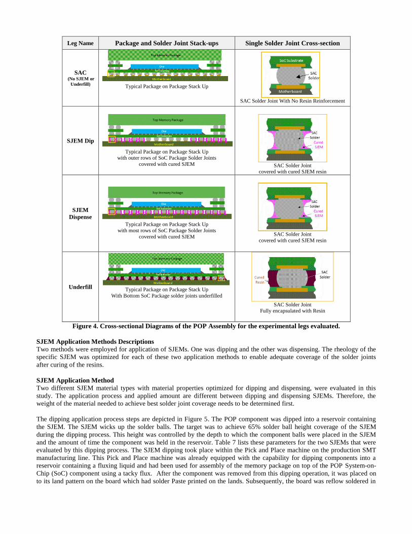
Leg Name Package and Solder Joint Stack-ups Single Solder Joint Cross-section
SAC (No SJEM or
Underfill) Typical Package on Package Stack Up
SAC Solder Joint With No Resin Reinforcement
SJEM Dip
Typical Package on Package Stack Up with outer rows of SoC Package Solder Joints
covered with cured SJEM
SAC Solder Joint
covered with cured SJEM resin
SJEM
Dispense
Typical Package on Package Stack Up
with most rows of SoC Package Solder Joints
covered with cured SJEM
SAC Solder Joint
covered with cured SJEM resin
Underfill Typical Package on Package Stack Up
With Bottom SoC Package solder joints underfilled
SAC Solder Joint Fully encapsulated with Resin
Figure 4. Cross-sectional Diagrams of the POP Assembly for the experimental legs evaluated.
SJEM Application Methods Descriptions
Two methods were employed for application of SJEMs. One was dipping and the other was dispensing. The rheology of the
specific SJEM was optimized for each of these two application methods to enable adequate coverage of the solder joints
after curing of the resins.
SJEM Application Method
Two different SJEM material types with material properties optimized for dipping and dispensing, were evaluated in this
study. The application process and applied amount are different between dipping and dispensing SJEMs. Therefore, the
weight of the material needed to achieve best solder joint coverage needs to be determined first.
The dipping application process steps are depicted in Figure 5. The POP component was dipped into a reservoir containing
the SJEM. The SJEM wicks up the solder balls. The target was to achieve 65% solder ball height coverage of the SJEM
during the dipping process. This height was controlled by the depth to which the component balls were placed in the SJEM
and the amount of time the component was held in the reservoir. Table 7 lists these parameters for the two SJEMs that were
evaluated by this dipping process. The SJEM dipping took place within the Pick and Place machine on the production SMT
manufacturing line. This Pick and Place machine was already equipped with the capability for dipping components into a
reservoir containing a fluxing liquid and had been used for assembly of the memory package on top of the POP System-on-
Chip (SoC) component using a tacky flux. After the component was removed from this dipping operation, it was placed on
to its land pattern on the board which had solder Paste printed on the lands. Subsequently, the board was reflow soldered in

an in-line oven using a typical reflow profile for SAC305 solder paste. During this reflow soldering step, the SJEM cured and
encapsulated the solder joints of the components
Figure 5. SJEM Dipping Process
Table 7 - Dip Materials and Process Comparison
Material Material/ Parameter Comparison
Viscosity Cure
Profile Dipping Height Others
Dip1 5-20k cps (Production
Viscometer, 0.5 rpm) SAC305
0.075mm (65% solder
ball hgt post SMT)
Part is held for 0.5 secs at placement
before nozzle release
Dip2 1050cps (Production Viscometer, 20 rpm)
SAC305 0.075mm (65% solder
ball hgt post SMT) Part is held for 0.35 secs at placement
before nozzle release
One issue was discovered during the dipping process development. The SoC substrate was warped slightly at room
temperature due to the presence of the silicon chip on the substrate. When the POP components were dipped into the
reservoir, the covered of the SJEM across all the rows was not uniform due to this substrate warpage. Figure 6 illustrates this
issue. The outer rows were covered adequately with the SJEM but the central rows were devoid of the SJEM after the dipping
operation. Dipping the component deeper into the SJEM reservoir would lead to excessive application of the SJEM on the
other rows and would sometimes even make it difficult to pull the component out of the reservoir. Therefore, the dipping
process acceptance limit was changed to ensure that at least three outer rows of solder balls were covered to the target limit
by the SJEM on each side of the package, as shown in Figure 6.
Figure 6 - Preferred Dipping SJEM material area coverage
The dispensing application process steps employed in this study are shown in Figure 7. The first three steps are identical to
that of a typical SMT process, and include printing of the solder paste on the lands, placement of the component on the land
pattern site and reflow soldering. The next step is to dispense the SJEM on one side of the package edge and then reflow
solder the board once again. This process step is similar to that for applying and underfilling. However, there are two key
differences. One is that the underfill requires a batch oven cure at a specific temperature and time. The other is that the SJEM
flows during its curing process, which is the reflow cycle. When dispensing underfill, time has to be set aside for the underfill
to flow into the gap between the package substrate and the board before it can be cured.
The dispensing process described above was chosen for this study after investigation of some other alternative process steps
for the dispensing application option. Initially, as recommended by the SJEM suppliers, the SJEM was dispensed on to each
individual land of the package. However, there were three unacceptable drawbacks to this method.
Firstly, due to the large number of lands for the POP component (220), the time taken to individually dispense each land was
deemed to be unacceptably long for a high volume production environment. Jetting of the SJEMs could alleviate this issue
since the jetting process is quicker than the needle dispensing process, but there was no jetting equipment on the SMT
manufacturing line at the time this study was being conducted.
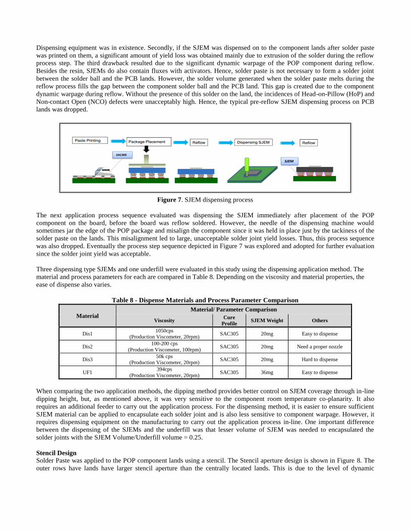
Dispensing equipment was in existence. Secondly, if the SJEM was dispensed on to the component lands after solder paste
was printed on them, a significant amount of yield loss was obtained mainly due to extrusion of the solder during the reflow
process step. The third drawback resulted due to the significant dynamic warpage of the POP component during reflow.
Besides the resin, SJEMs do also contain fluxes with activators. Hence, solder paste is not necessary to form a solder joint
between the solder ball and the PCB lands. However, the solder volume generated when the solder paste melts during the
reflow process fills the gap between the component solder ball and the PCB land. This gap is created due to the component
dynamic warpage during reflow. Without the presence of this solder on the land, the incidences of Head-on-Pillow (HoP) and
Non-contact Open (NCO) defects were unacceptably high. Hence, the typical pre-reflow SJEM dispensing process on PCB
lands was dropped.
Figure 7. SJEM dispensing process
The next application process sequence evaluated was dispensing the SJEM immediately after placement of the POP
component on the board, before the board was reflow soldered. However, the needle of the dispensing machine would
sometimes jar the edge of the POP package and misalign the component since it was held in place just by the tackiness of the
solder paste on the lands. This misalignment led to large, unacceptable solder joint yield losses. Thus, this process sequence
was also dropped. Eventually the process step sequence depicted in Figure 7 was explored and adopted for further evaluation
since the solder joint yield was acceptable.
Three dispensing type SJEMs and one underfill were evaluated in this study using the dispensing application method. The
material and process parameters for each are compared in Table 8. Depending on the viscosity and material properties, the
ease of dispense also varies.
Table 8 - Dispense Materials and Process Parameter Comparison
Material Material/ Parameter Comparison
Viscosity Cure
Profile SJEM Weight Others
Dis1 1050cps
(Production Viscometer, 20rpm) SAC305 20mg Easy to dispense
Dis2 100-200 cps
(Production Viscometer, 100rpm) SAC305 20mg Need a proper nozzle
Dis3 50k cps
(Production Viscometer, 20rpm) SAC305 20mg Hard to dispense
UF1 394cps
(Production Viscometer, 20rpm) SAC305 36mg Easy to dispense
When comparing the two application methods, the dipping method provides better control on SJEM coverage through in-line
dipping height, but, as mentioned above, it was very sensitive to the component room temperature co-planarity. It also
requires an additional feeder to carry out the application process. For the dispensing method, it is easier to ensure sufficient
SJEM material can be applied to encapsulate each solder joint and is also less sensitive to component warpage. However, it
requires dispensing equipment on the manufacturing to carry out the application process in-line. One important difference
between the dispensing of the SJEMs and the underfill was that lesser volume of SJEM was needed to encapsulated the
solder joints with the SJEM Volume/Underfill volume = 0.25.
Stencil Design
Solder Paste was applied to the POP component lands using a stencil. The Stencil aperture design is shown in Figure 8. The
outer rows have lands have larger stencil aperture than the centrally located lands. This is due to the level of dynamic
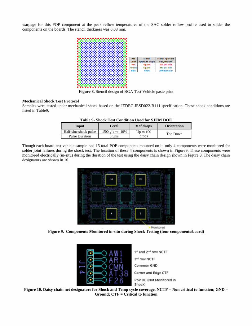
warpage for this POP component at the peak reflow temperatures of the SAC solder reflow profile used to solder the
components on the boards. The stencil thickness was 0.08 mm.
Figure 8. Stencil design of BGA Test Vehicle paste print
Mechanical Shock Test Protocol
Samples were tested under mechanical shock based on the JEDEC JESD022-B111 specification. These shock conditions are
listed in Table9.
Table 9- Shock Test Condition Used for SJEM DOE
Input Level # of drops Orientation
Half-sine shock pulse 1500 g’s +/- 10% Up to 100
drops Top Down
Pulse Duration 0.5ms
Though each board test vehicle sample had 15 total POP components mounted on it, only 4 components were monitored for
solder joint failures during the shock test. The location of these 4 components is shown in Figure9. These components were
monitored electrically (in-situ) during the duration of the test using the daisy chain design shown in Figure 3. The daisy chain
designators are shown in 10.
Figure 9. Components Monitored in-situ during Shock Testing (four components/board)
Figure 10. Daisy chain net designators for Shock and Temp cycle coverage. NCTF = Non critical to function; GND =
Ground; CTF = Critical to function

The shock test samples were setup with the board placed in a fixture in the top down orientation on a High-G shock table.
This setup is shown in Figure 11.
Figure 11. Shock Test Setup
Temperature Cycling Test Protocol
The temperature cycling test profile is shown in Figure 12. It entailed dwell temperatures of -40C and 125C, with a 5min
soak at each dwell temperature and a 15C/min ramp between the dwell temperatures. The total cycle time was ~32min/cycle.
Temp cycle data collection was carried out per the JEDEC JESD22-A104E specification. The component is deemed failed
when the resistance of the daisy chains being monitored exceeded 1 MΩ.
Figure 12. Temp Cycle Test Profile
A production thermal shock ramp tester was used was used to conduct the experiment. All 15 assembled POP components on
the test board were monitored for solder joint failures. These 15 locations are shown in Figure 13.
Figure 13: Components monitored in-situ during Temp Cycle testing
Results and Discussion
SJEM Assembly Results
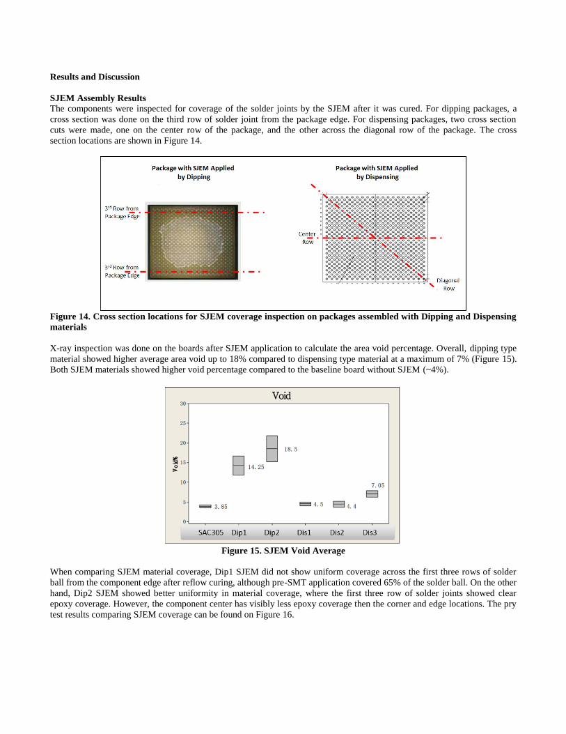
The components were inspected for coverage of the solder joints by the SJEM after it was cured. For dipping packages, a
cross section was done on the third row of solder joint from the package edge. For dispensing packages, two cross section
cuts were made, one on the center row of the package, and the other across the diagonal row of the package. The cross
section locations are shown in Figure 14.
Figure 14. Cross section locations for SJEM coverage inspection on packages assembled with Dipping and Dispensing
materials
X-ray inspection was done on the boards after SJEM application to calculate the area void percentage. Overall, dipping type
material showed higher average area void up to 18% compared to dispensing type material at a maximum of 7% (Figure 15).
Both SJEM materials showed higher void percentage compared to the baseline board without SJEM (~4%).
Figure 15. SJEM Void Average
When comparing SJEM material coverage, Dip1 SJEM did not show uniform coverage across the first three rows of solder
ball from the component edge after reflow curing, although pre-SMT application covered 65% of the solder ball. On the other
hand, Dip2 SJEM showed better uniformity in material coverage, where the first three row of solder joints showed clear
epoxy coverage. However, the component center has visibly less epoxy coverage then the corner and edge locations. The pry
test results comparing SJEM coverage can be found on Figure 16.
Figure 16. SJEM Dipping Material Coverage (Left: SJEM Dip1; Right: SJEM Dip2)
Dispensing type SJEM material showed more epoxy encapsulation around the solder joints overall compared to dipping type
material. The localized dispensing offered more material coverage. Dis1 and Dis2 SJEM both showed full material coverage
on all solder balls across the package after curing (Figure 17). Pry test was unsuccessful on Dis3 samples after five attempts
due to strong adhesion to the PCB, so the coverage amount is unknown. This observation also indicated that Dis3 material
processability and reworkability could be a potential challenge.
Figure 17. SJEM Dispensing Material Coverage (Left: Dis1; Right: Dis2)
In addition to the pry test, cross sectioning was also done on both dipping and dispensing samples on material coverage
following the cross section location in Figure 14. No material coverage was found on the first row of solder balls on Dip1,
which supported the non-uniformity found from the pry test. For Dip2, some voiding was found near the package, but
material coverage can be found up to the thrid row of solder balls, showing better uniformity (Figure 18 and 19).
Figure 18. SJEM Dip1 cross section on the first row of package edge
Figure 19. SJEM Dip2 cross section on the third row of package edge
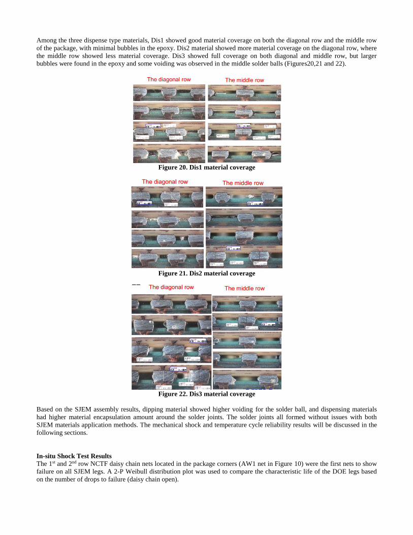
Among the three dispense type materials, Dis1 showed good material coverage on both the diagonal row and the middle row
of the package, with minimal bubbles in the epoxy. Dis2 material showed more material coverage on the diagonal row, where
the middle row showed less material coverage. Dis3 showed full coverage on both diagonal and middle row, but larger
bubbles were found in the epoxy and some voiding was observed in the middle solder balls (Figures20,21 and 22).
Figure 20. Dis1 material coverage
Figure 21. Dis2 material coverage
Figure 22. Dis3 material coverage
Based on the SJEM assembly results, dipping material showed higher voiding for the solder ball, and dispensing materials
had higher material encapsulation amount around the solder joints. The solder joints all formed without issues with both
SJEM materials application methods. The mechanical shock and temperature cycle reliability results will be discussed in the
following sections.
In-situ Shock Test Results
The 1st and 2nd row NCTF daisy chain nets located in the package corners (AW1 net in Figure 10) were the first nets to show
failure on all SJEM legs. A 2-P Weibull distribution plot was used to compare the characteristic life of the DOE legs based
on the number of drops to failure (daisy chain open).

The 2-P Weibull distribution data plots for the 1st and 2nd row NCTF are shown in Figure 23. Table 10 lists these results in
terms of the characteristics lives of the data, i.e., number of drops for 63.2% failure rate. In summary, both SJEM showed
improved shock performance over bare component without SJEM (Control Leg). Dip1 and Dip2 material showed comparable
characteristic lives, but Dip1 material has a larger data variation, which can be attributed to the coverage uniformity observed
from Dip1 assembly results. Both Dis1 and Dis2 material showed comparable shock performance compared to dipping
material, while Dis3 is the only SJEM that did not show in-situ shock failures. Underfill (UF1) material also performed better
than most SJEM, with only 1 failed samples among a total of 45 samples. Based on the results, SJEM still has room for
improvement to achieve shock performance parity to replace underfill material.
Figure 23: Weibull 2-P distribution of Net AW1 (1st and 2nd row NCTF) comparing Dipping SJEM, Dispensing SJEM,
and Blank Board. Green: Blank; Black: Dis1; Yellow: Dis2; Pink: Dip1; Blue: Dip2
Table 10 - Shock Characteristic Life comparison for Various DOE Legs
DOE Leg Characteristic Life (63.2% fail) in Number of Drops
for the AW1 Net (1st &2nd Outer Rows)
Blank (Control) 37
Dip1 112
Dip2 101
Dis1 60
Dis2 97
Dis3 No Fail
UF1 No Fail
Overall, Dis1 material showed the lowest number of drops to failure when compared to the rest of the SJEMs evaluated. But
it still showed a 62% improvement over boards without SJEM. The two dipping materials showed marginally better shock
performance than two of the three dispensing materials. This can be attributed a larger amount of material around the solder
joint, but this effect needs further study.
In general, these results highlight the necessity of additional work to optimize SJEM rheological properties and curing
kinetics and ensure that the coverage of the SJEM cured resins is more uniform. Cured resin adhesion and cohesive properties
also need improve to enable solder joints encapsulated with SJEMs have comparable shock resistance to underfilled solder
joints.

Temperature Cycle Test Results
The temperature cycle test was carried out to 500 cycles, with intermittent readouts taken at every 100cycles. Failure was
observed on bare board, underfill and dispensing SJEM legs on the first two monitored daisy chain nets.
A 2-P Weibull distribution using Maximum Likelihood (MLE) method was used to analyze the intermittent resistance data
collected per the JEDEC JESD22-A104-B specification. From the Weibull distribution shown in Figure 24, and Table 11,
which lists the characteristic life for all legs, dipping material showed overall best temp cycle performance.
Figure 24. Weibull 2-P distribution of Blank versus SJEM Dispensing versus Underfill on AW1 (1st and 2nd row
NCTF). Dipping leg is not plotted because no failures were detected (Black: UF1; Green: Dis1; Yellow: Dis2; Blue:
Bare Board; Pink: Dis3)
The Weibull results showed that the reliability of SJEM boards can be material property and epoxy coverage dependent.
Although dipping SJEM boards has less material coverage, the temperature cycle reliability is better than the dispensing
material. The resin encapsulation amount surrounding the solder joint can play an important role on thermal cycle fatigue
failure especially when the material properties such as Tg or CTE is not optimized for the temperature use condition.
Accelerated temperature cycle test shows early failure due to CTE mismatch and exceeding the glass transition temperature.
More will be discussed in the failure analysis section in this paper as we compare the failure location on different SJEM
materials.
Table 12 lists the temperature cycle failures after each 100 cycle readout for each of the legs tested. Based on the results from
this study, both SJEM material type showed at least 1.9x better temperature cycle reliability than underfill material. The
underfill material evaluated in this study showed worse reliability than blank boards.
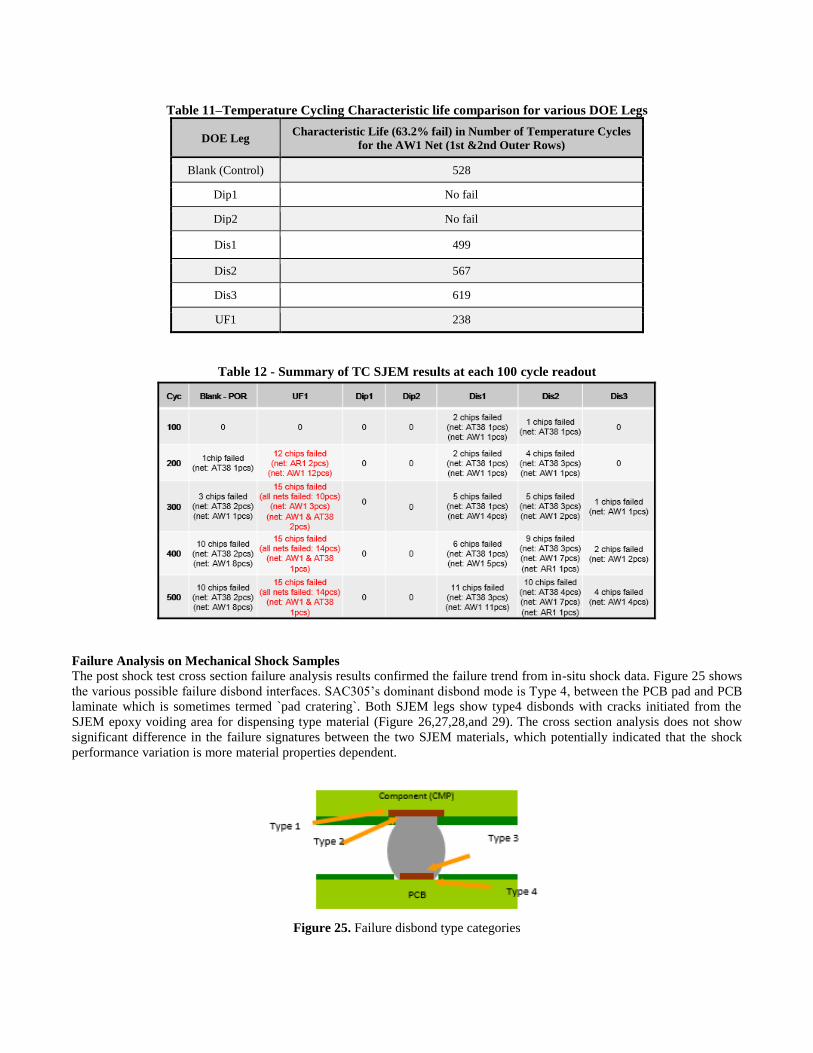
Table 11–Temperature Cycling Characteristic life comparison for various DOE Legs
DOE Leg Characteristic Life (63.2% fail) in Number of Temperature Cycles
for the AW1 Net (1st &2nd Outer Rows)
Blank (Control) 528
Dip1 No fail
Dip2 No fail
Dis1 499
Dis2 567
Dis3 619
UF1 238
Table 12 - Summary of TC SJEM results at each 100 cycle readout
Failure Analysis on Mechanical Shock Samples
The post shock test cross section failure analysis results confirmed the failure trend from in-situ shock data. Figure 25 shows
the various possible failure disbond interfaces. SAC305’s dominant disbond mode is Type 4, between the PCB pad and PCB
laminate which is sometimes termed `pad cratering`. Both SJEM legs show type4 disbonds with cracks initiated from the
SJEM epoxy voiding area for dispensing type material (Figure 26,27,28,and 29). The cross section analysis does not show
significant difference in the failure signatures between the two SJEM materials, which potentially indicated that the shock
performance variation is more material properties dependent.
Figure 25. Failure disbond type categories

Figure 26. Post Mechanical Shock Cross section failure interface for All Experimental Legs
Figure 27. Evidence of Dis1 material crack initiation site in the SJEM cured Resin
Figure 28.Evidence of Dis2 material crack initiation site in the SJEM cured Resin
Figure 29. Evidence of Dis3 material crack initiation site in the SJEM cured Resin
Failure Analysis on Temperature Cycle Samples
Cross sections were done immediately after reflow soldering (i.e., pre temperature cycling) on package locations shown in
Figures18,19,20,21, and22 in the earlier section of this paper to determine the extent of resin encapsulation height on the
solder joints. More material coverage was found on corner/edge package location compared to package center on dipping
material, whereas dispensing type material showed full coverage around all solder joints regardless of location on the
package. This variation in resin coverage also lead to the temp cycle characteristic life margin differences observed on SJEM
and SAC305 at 1st and 2nd NCTF net. More details will be discussed in the section below.
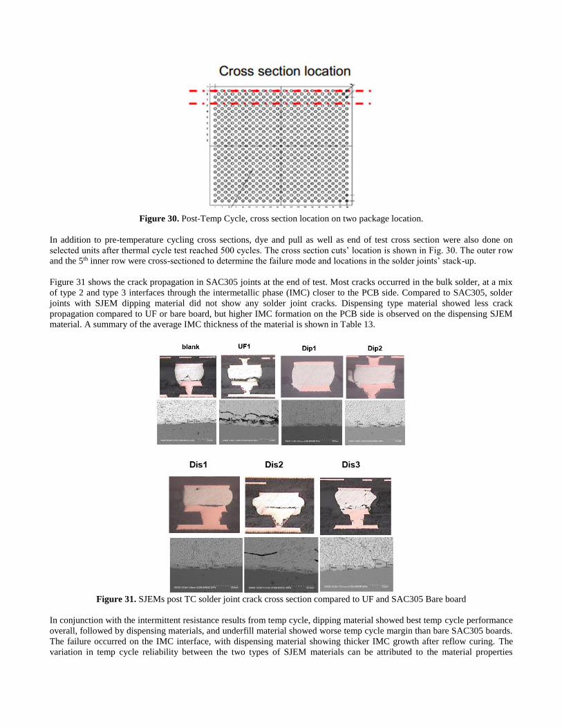
Figure 30. Post-Temp Cycle, cross section location on two package location.
In addition to pre-temperature cycling cross sections, dye and pull as well as end of test cross section were also done on
selected units after thermal cycle test reached 500 cycles. The cross section cuts’ location is shown in Fig. 30. The outer row
and the 5th inner row were cross-sectioned to determine the failure mode and locations in the solder joints’ stack-up.
Figure 31 shows the crack propagation in SAC305 joints at the end of test. Most cracks occurred in the bulk solder, at a mix
of type 2 and type 3 interfaces through the intermetallic phase (IMC) closer to the PCB side. Compared to SAC305, solder
joints with SJEM dipping material did not show any solder joint cracks. Dispensing type material showed less crack
propagation compared to UF or bare board, but higher IMC formation on the PCB side is observed on the dispensing SJEM
material. A summary of the average IMC thickness of the material is shown in Table 13.
Figure 31. SJEMs post TC solder joint crack cross section compared to UF and SAC305 Bare board
In conjunction with the intermittent resistance results from temp cycle, dipping material showed best temp cycle performance
overall, followed by dispensing materials, and underfill material showed worse temp cycle margin than bare SAC305 boards.
The failure occurred on the IMC interface, with dispensing material showing thicker IMC growth after reflow curing. The
variation in temp cycle reliability between the two types of SJEM materials can be attributed to the material properties
differences where dipping material has more desirable CTE and Tg that will minimize temp cycle reliability risk. With
dispensing material, although there was more material coverage, the properties might not be optimized for temp cycle
reliability, which subsequently led to negative impact on temp cycle margin due to thicker IMC growth and worse CTE
mismatch.
Table 13 - Post temp cycle IMC thickness comparison between SJEMs, UF, and SAC305
DOE Average IMC thickness (μm) Reflow Cycles Exposure
Blank (Control) 2.64 1
Dip1 2.65 1
Dip2 2.52 1
Dis1 3.81 2
Dis2 3.95 2
Dis3 3.06 2
UF1 2.45 1
CONCLUSIONS
This study set out to determine the processability, mechanical and temperature cycle reliability of SAC BGA solder joints
reinforced by encapsulation using SJEMs. A total of 5 different SJEMs from two suppliers were evaluated. Three of these
SJEMS were applied by dipping the BGA package balls into a reservoir containing these SJEMs and two others were applied
by dispensing along one edge the package after it was initially reflow soldered. The solder joint reliability enhancement
provided by the SJEMs was compared to a selected underfill material.
From the process assembly results, all SJEMs types can be successfully applied and cured with a typical SAC305 reflow
process without solder joint defects. When comparing the two application methods, the dipping method provided a better
control on SJEM coverage through in-line dipping height, but the number of solder balls covered by the SJEM in the BGA
array was very sensitive to the room temperature coplanarity of the component. The dipping method requires an additional
feeder to carry out the application process. The dispensing method ensured sufficient SJEM material coverage each solder
joint and was less sensitive to component warpage. However, this method requires additional dispensing equipment to carry
out the application process. The SJEMs covered solder joints formed by the dipping method contained slightly higher voiding
when compared to the SJEM covered solder joints formed by the dispensing method. The dispensing method resulted in more
volume of SJEM around the solder joints as well as better uniformity of this volume across the solder joint array for a
package. However, this larger volume of SJEMs surrounding the solder joint can potentially make reworking the component
more difficult.
Based on in-situ failures recorded during the shock event which the POP components were subjected to, solder joints
reinforced with all SJEMs showed better mechanical shock margin when compared to the solder joints without any SJEMs
(the control leg). This confirmed that use of SJEMs do enhance the shock reliability of POP components. Among the various
SJEM materials evaluated, the Dis3 SJEM and the underfill material, performed the best and did not show any in-situ shock
failures. SJEMs applied by the dipping method showed slightly better margin than those applied by the dispensing method.
Based on the observed characteristic life on the1st and 2nd row NCTF nets, the ranking of the SJEMs according to the shock
resistance of the solder joints formed when using them is: Bare board < Dis1 < Dis2 =< Dip2 < Dip1 <Dis3 & UF.
Based on in-situ failures recorded during temperature cycling of the POP components, solder joints at the package corners
formed when using dipping SJEMs showed improved temperature cycle performance then the control sample which had no
SJEM reinforcement (the control leg). But, solder joints applied with dispensing SJEMs, did not show any significant
difference when compared to the control leg. The underfill material evaluated in this study showed a negative impact to temp
cycle reliability, with the failure occurring even before the control leg. Based on the observed characteristic life on the 1st
and 2nd row corner NCTF nets, the ranking of the SJEMs according to the enhancement they provide in improving the solder
joint temp cycle failure resistance is: Dipping > Dispensing ≥ Bare Board > UF. Dispensing SJEMs showed thicker IMC
formation on the PCB side compared to the rest of the DOE legs.
From these results, all SJEM materials evaluated exhibited feasibility to be applied, reflowed, and cured with SAC305 solder
paste. The dipping method is sensitive to package coplanarity, but resulted in better reliability in mechanical shock and
temperature cycle. The dispensing method provides more material coverage, but this does not translate to better shock or
temp cycle reliability. The material properties of the cured SJEM resins and IMC thickness and morphology of the solder
joints both play a role in optimizing reliability performance. Hence, further work is necessary to understand the effect of resin
properties and the amount of resin coverage of the solder joints on their reliability performance. When comparing SJEM
materials to underfills, though temp cycle reliability is shown to be equivalent or better for SJEMs, there is still room for
enhancing the mechanical shock reliability.
In summary, the weighted matrix comparing all the DOE legs for various characteristics is shown in Table 14 below. From
this table, dipping SJEM is the most favorable solution from this study, which showed improved reliability margin over bare
boards. It can also be a potential solution to replace traditional underfill material to provide solder joint reinforcement as
component pitch size decreases and body size increases.
Table 14 - Overall matrix comparison: 6 – Most desirable; 1 – least desirable
Polymeric
Reinforcement
Ease of Processing and
Solder Joint Yield
Temperature
Cycling Reliability
Drop shock
reliability
Mfg Line
Loading level Cost Total
Control (Blank) 6 1 1 6 6 20
Underfill UF1 4 0.45 6 1 1 12.45
SJEM Dis1 4 1.07 1.6 4 4 14.67
SJEM Dis2 4 1 2.6 4 4 15.6
SJEM Dis3 2 2.4 6 4 4 18.4
SJEM Dip1 2 6 3 5.5 5.5 22
SJEM Dip2 4 6 2.7 5 5 22.7
ACKNOWLEDGEMENTS
The authors would like to acknowledge Russ Brown, and Quanta reliability test lab for their contributions and support to
SMT, testing, and failure analysis shared in this paper. The authors would also like to acknowledge their management for the
valuable guidance and inputs during the course of this year long work, without which this would not have been possible.
References
[1] “Solder joint reliability prediction of flip chip packages under shock
loading environment", W. K. Loh, Proc. InterPACK'05 Conf., San Francisco, CA, Jul. 17-25, 2005.
[2] "The effect of corner glue on BGA package temperature cycling
performance: A modeling study", M. Pei, R. Han, Y. Ge, S. Goyal, V. Rajarathinam, M. Mukadam, IEEE ECTC, pp.
1494-1499, 2013.
[3] “A Rapidly Changing Test Landscape”, Brian Swiggett, 13th European
Manufacturing Test Conference (EMTC), 2014
[4] “The Future of Packaging and Assembly Technology”, Jan Vardaman,
Techsearch International, Presentation given to Central-Texas SMTA Chapter Meeting, 2016.
[5] “The Application of Bi-based Solders for Low Temperature Reflow to
Reduce Cost while Improving SMT Yields in Client Computing Systems”, S. Mokler, Presentation given at 2016 SMTA
International Conference, Chicago, IL.
[6] “iNEMI Technology Roadmaps”, B. Bader, Presentation given at the
ICEP Kyoto Conference, April 16, 2015.”
[7] “Mechanical Properties of Metals”, Martin Tarr,
http://www.mtarr.co.uk/courses/topics/0123_mpm/index.html.
[8] “Underfill Encapsulants and Edge bond Adhesives for Enhancing of
Board Level Reliability”, S. Chang, E. S. Ibe, and K. I. Loh, Proceedings of the SMTA International Conference, 2013.
[9] “Next Generation Board Level Underfill (BLUF) for Fine Pitch BGA and
POP”, S.M.Yeo, C.S.Tay, C.C. Chong, J.S. Beh, Proceedings of the SMTA International Conference, 2010.
[10] “A Comprehensive Analysis of the Thermal Cycling Reliability of Lead
Free Chip Scale Package Assemblies with Various Reworkable Board-Level Polymeric Strategies”, H. Shi, C. Tian, D.
Yu and T. Ueda, 2012 International Conference on Electronic Packaging Technology and High Density Packaging,
2012, pp 959-970.
[11] “WLCSP and BGA Reworkable Underfill Evaluation and Reliability”, F.
Xie, H. Wu, D.F. Baldwin, S. Bhattacharya, and K. Hodge, Proceedings of the SMTA International Conference, 2015.
[12] “Manufacturability Assessments of Board Level Adhesives on Fine Pitch
Ball Grid Array Components”, V. Rajarathinam, J. Wade, A. Donaldson, R. Aspandiar, D. Chelladurai and S. Mokler,
Proceedings of the SMTA International Conference, 2013.
[13] “Board-Level Shear, Bend, Drop and Thermal Cycling Reliability of
Lead-Free Chip Scale Packages with Partial Underfill: A Low-Cost Alternative to Full Underfill”, H. Shi, C. Tian, M.
Pecht, and T. Ueda, Proceedings of the 2012 IEEE 14th Electronics Packaging Technology Conference, pp. 774-785.
[14] “Underfill Flow as Viscous Flow Between Parallel Plates Driven by
Capillary Action”, M. K. Schwiebert and W.H. Leong, IEEE Transactions On Components, Packaging, and
Manufacturing Technology,Part C, Vol. 19, No. 2, April 1996
[15] “Material Issues in Area Array Packaging”, D.R.Frear, JOM, Vol. 51,
No. 3, 1999.
[16] “Influence of Gap Height in Flip Chip Underfill Process with Non-
Newtonian Flow between Two Parallel Plates”, C. Y. Khor, M. Z. Abdullah, M. Abdul Mujeebu, Journal of Electronic
Packaging, Vol. 134, March, 2012.
[17] “A Theoretical Analysis of the Concept of Critical Clearance Toward a
Design Methodology for the Flip-Chip Package”, J.W.Wan, W.J Zhang, D.W. Bergstrom, Journal of Electronic
Packaging, Vol. 129, March, 2007, 473-478.
[18] “Capillary Underfill Physical Limitations for Future Packages”, H.
Quinones and T. Ratledge, Proceedings of the Pan Pacific Conference, 2010, Hawaii.
[19] “The Chemistry and Physics of Underfill”, K. Gilleo, Proceedings of
NEPCON West, March 1998, pp. 280-292.
[20] “Evaluation of High Reliability Reworkable Edge Bond Adhesives for
BGA Applications”, F. Xie, H. Wu, D. F. Baldwin, S. Bhattacharya, K. Hodge and Q. Ji, Proceedings of the SMTA
International Conference, 2015
[21] “Factors Impacting Solder Extrusion in Reworkable Underfills”, N.
Poole, Proceedings of the SMTA International Conference, 2013
[22] “New Underfill Materials Designed for Increasing Reliability of Fine-
Pitch Wafer Level Devices”, B. J. Toleno, S. Hu, H. Yoo, and R. Zhang, Proceedings of the SMTA South East Asia
Conference, 2014, Penang, Malaysia.
[23] “Effects of Edge and Corner Bond Adhesives on the Drop Reliability of
Package-on-Package Bottom Package Assemblies”, H.Shi and T Ueda, Proceedings of the 3rd International Conference
on Computer Research and Development, 2011, pp. 416-420.
[24] “Negative Impact of Certain Adhesive Configurations on Solder Joint
Reliability of Package on Package Architecture: A Comprehensive Experimental and Numerical Study”, S. Tripathi, R.
Han, and M. Vujosevic, 15th IEEE Intersociety Conference on Thermal and Thermomechanical Phenomena in
Electronic Systems (ITherm), 2016, pp.871-876.
[25] “Accessing Adhesive Induced Risk for BGAs in Temperature Cycling”,
G. Arakere, M. Vujosevic and M. Pei, Proceedings of the IEEE 64th Electronic Components and Technology
Conference (ECTC), 2014, pp. 395 - 403,
[26] “A First Individual Solder Joint Encapsulant Adhesive”, M. Liu and W.
Yin, Proceedings of 2010 IMAPS, Raleigh, NC
[27] “Solder Joint Encapsulation and Reliability using Dippable Underfill”,
Y.C Yeo, M. Huang, F.X. Che, S.C. Chong, K.C.S. Lim, S.Thew, N.S. Vasarla and S. Gao, Proceedings of the 12th
Electronic Packaging Technology Conference, 2010
[28] “Epoxy Flux Bridges the Gap to Low Cost No-Clean Flip Chip Assembly”, W.Yin, G. Beckwith, H-S Hwang, L.
Kresge, N-C, Lee, Proceedings of the SMTA International Conference, 2012.
[29] “Epoxy Fluxes: DIP Assembly Process Issues and Reliability”, P.
Kondos, M. Meilunas and M. Anselm, Proceedings of the SMTA International Conference, 2012.
[30] “A Novel Epoxy Flux On Solder Paste For Assembling Thermally
Warped POP”, N-C. Lee, Proceedings of 2013 IMAPS, Orlando, FL.
[31] “Epoxy Flux Material and Process for Enhancing Electrical
Interconnections”, N. Poole, E Vasquez, and B. Toleno, Proceedings of the SMTA International Conference, 2015.
[32] “Epoxy Flux Technology – Tacky Flux with Value Added Benefits”, B.
Chan, Q. Ji, M. Currie, N. Poole, C.T. Tu, Proceedings of the 59th Electronic Components and Technology Conf
(ECTC), 2009, pp. 188-190.
[33] “Reflow-Curable Polymer Fluxes For Flip Chip Assembly”, R. W.
Johnson, M. A. Capote, Z. M. Zhou, S. Chu, and L. Zhou, Proceedings of the Surface Mount International (SMI)
Conference, 1997,pp.267-272.
[34] “Processing of Fluxing Underfills for Flip Chip-on-Laminate Assembly”,
R. Zhao, R. W. Johnson, G.Jones, E. Yaeger, M. Konarski,P. Krug, and L. L. Crane, IEEE Transactions on Electronics
Packaging Manufacturing, Vol. 26, No. 1, 2003.
[35] “Board Level Drop Test Methods for Handheld Electronics”, JESD22-B111, JEDEC, 2003.
[36] “Temperature Cycling”, JESD22-A104E, JEDEC, October 2014.