Embed Size (px)
Citation preview
APPENDIX A
SHORT QUESTIONS AND ANSWERS
Unit – I
Boolean Algebra and Logic Gates
Part - A
1. Define binary logic?
Binary logic consists of binary variables and logical operations. The variables
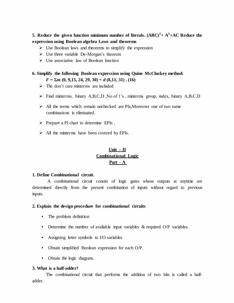
are designated by the alphabets such as A, B, C, x, y, z, etc., with each variable having
only two distinct values: 1 and 0. There are three basic logic operations: AND, OR, and
NOT.
2. What are the basic digital logic gates?
The three basic logic gates are
AND gate
OR gate
NOT gate
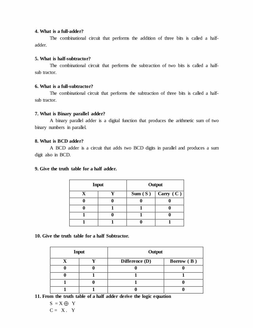
3. What is a Logic gate?
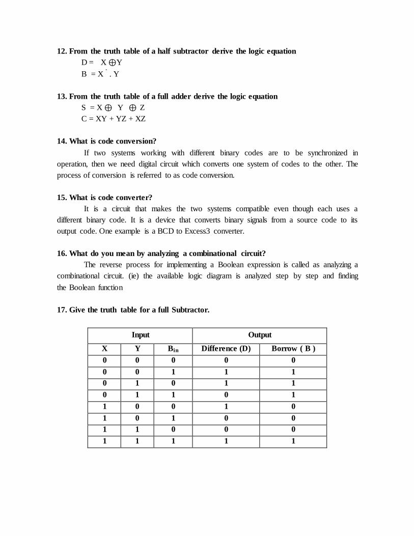
Logic gates are the basic elements that make up a digital system. The electronic
gate is a circuit that is able to operate on a number of binary inputs in order to perform a
particular logical function.
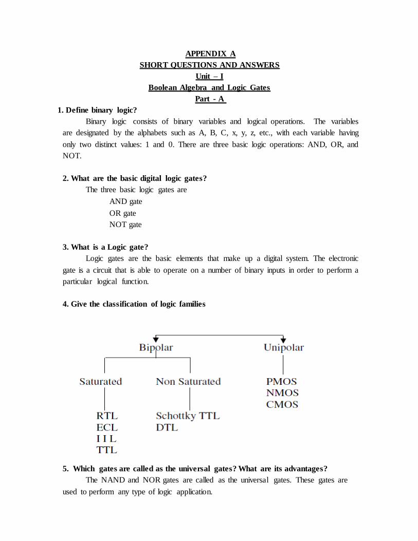
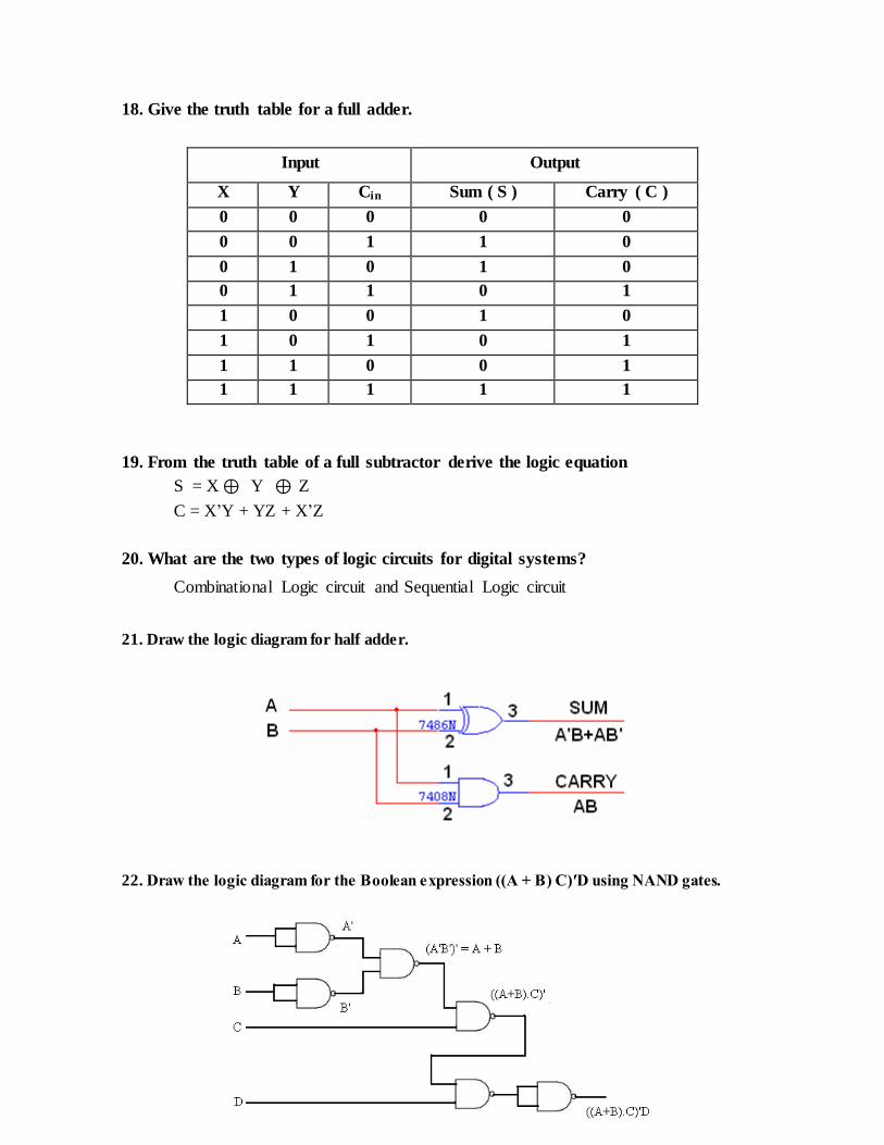
4. Give the classification of logic families
5. Which gates are called as the universal gates? What are its advantages?
The NAND and NOR gates are called as the universal gates. These gates are
used to perform any type of logic application.
6. Classify the logic family by operation?
The Bipolar logic family is classified into
Saturated logic
Unsaturated logic.
The RTL, DTL, TTL, I2L, HTL logic comes under the saturated logic family.
The Schottky TTL, and ECL logic comes under the unsaturated logic family.
7. Define Fan-out?
Fan out specifies the number of standard loads that the output of the gate can
drive without impairment of its normal operation.
8. Define power dissipation?
Power dissipation is measure of power consumed by the gate when fully driven
by all its inputs.
9. What is propagation delay?
Propagation delay is the average transition delay time for the signal to propagate
from input to output when the signals change in value. It is expressed in ns.
10. Define noise margin?
It is the maximum noise voltage added to an input signal of a digital circuit that
does not cause an undesirable change in the circuit output. It is expressed in volts.
11. Define fan in?
Fan in is the number of inputs connected to the gate without any degradation
in the voltage level.
12. What is Operating temperature?
All the gates or semiconductor devices are temperature sensitive in nature.
The temperature in which the performance of the IC is effective is called as
operating temperature. Operating temperature of the IC vary from 00 C to 700 c.
13. What is High Threshold Logic?
Some digital circuits operate in environments, which produce very high noise
signals. For operation in such surroundings there is available a type of DTL gate
which possesses a high threshold to noise immunity. This type of gate is called HTL
logic or High Threshold Logic.
14. Which gate is equal to AND-invert Gate?
NAND gate.
15. Which gate is equal to OR-invert Gate?
NOR gate.
16. Bubbled OR gate is equal to NAND gate
17. Bubbled AND gate is equal to NOR gate
18. Define the term digital.
The term digital refers to any process that is accomplished using discrete units
19. What is meant by bit?
A binary digit is called bit
20. What is the best example of digital system?
Digital computer is the best example of a digital system.
21. Define byte?
A group of 8 bits.
22. List the number systems?
i) Decimal Number system
ii) Binary Number system
iii) Octal Number system
iv) Hexadecimal Number system
23. State the sequence of operator precedence in Boolean expression?
i) Parenthesis
ii) NOT
iii) AND
iv) OR
24. What is the abbreviation of ASCII and EBCDIC code?
ASCII-American Standard Code for Information Interchange. EBCDIC-Extended
Binary Coded Decimal Information Code.
25. What are the different types of number complements?
i) 1‟sComplement (r-1‟s complement)
ii) 2‟s Complement (r‟s complement)
26. Why complementing a number representation is needed?
Complementing a number becomes as in digital computer for simplifying the
subtraction operation and for logical manipulation complements are used.
27. How to represent a positive and negative sign in computers?
Positive (+) sign by 0
Negative (-) sign by 1.
28. What is meant by Map method?
The map method provides a simple straightforward procedure for minimizing
Boolean function.
29. What is meant by two variable map?
Two variable map have four minterms for two variables, hence the map consists of
four squares, one for each minterm
30. What is meant by three variable map?
Three variable map have 8 minterms for three variables, hence the map consists of 8
squares, one for each minterm
31. What is the use of Don’t care conditions?
Any digital circuit using this code operates under the assumption that these unused
combinations will never occur as long as the system
32. Express the function f(x, y, z)=1 in the sum of minterms and a product of
maxterms?
Minterms=∑ (0,1,2,3,4,5,6,7)
Maxterms=Nomaxterms.
33. What is the algebraic function of Exclusive-OR gate and Exclusive-NOR gate?
F=xy‟+x‟y
F=xy +x‟y‟
34. What are the methods adopted to reduce Boolean function?
i) Karnaugh map
ii) Tabular method or Quine mccluskey method
iii) Variable entered map technique.
35. Why we go in for tabulation method?
This method can be applied to problems with many variables and has the advantage
of being suitable for machine computation.
36. State the limitations of Karnaugh map.
i) Generally it is limited to six variable map (i.e.) more than six variable involving
expressions are not reduced.
ii) The map method is restricted in its capability since they are useful for simplifying
only Boolean expression represented in standard form.
37. What is tabulation method?
A method involving an exhaustive tabular search method for the minimum
expression to solve a Boolean equation is called as a tabulation method.
38. What are prime-implicants?
The terms remained unchecked are called prime-implicants. They cannot be reduced
further.
40. Explain or list out the advantages and disadvantages of K-map method?
The advantages of the K-map method are
i. It is a fast method for simplifying expression up to four variables.
ii. It gives a visual method of logic simplification.
iii. Prime implicants and essential prime implicants are identified fast.
iv. Suitable for both SOP and POS forms of reduction.
The disadvantages of the K-map method are
i. It is not suitable for computer reduction.
ii. K-maps are not suitable when the number of variables involved exceed four.
iii. Care must be taken to fill in every cell with the relevant entry, such as a 0, 1 (or)
don‟t care terms.
41. List out the advantages and disadvantages of Quine-Mc Cluskey method?
The advantages are,
a. This is suitable when the number of variables exceed four.
b. Digital computers can be used to obtain the solution fast.
c. Essential prime implicants, which are not evident in K-map, can be clearly seen in the
final results.
The disadvantages are,
a. Lengthy procedure than K-map.
b. Requires several grouping and steps as compared to K-map.
c. It is much slower.
d. No visual identification of reduction process.
e. The Quine Mc Cluskey method is essentially a computer reduction method.
42. Define Positive Logic.
When high voltage or more positive voltage level is associated with binary „1‟ and
while the low or less positive level is associated with binary „0‟ then the system adhering to
this is called positive logic.
43. Define Negative Logic.
When high voltage level is associated with binary „0‟ and whiles the low level is
associated with binary „1‟ then the system adhering to this is called negative logic.
44. List the characteristics of digital Ics
i) propagation delay
ii) power dissipation
iii) Fan-in
iv) Fan-out
v) Noise margin
45. Why parity checker is needed?
Parity checker is required at the receiver side to check whether the expected parity
is equal to the calculated parity or not. If they are not equal then it is found that the received
data has error.
46. What is meant by parity bit?
Parity bit is an extra bit included with a binary message to make the number of 1‟s
either odd or even. The message, including the parity bit is transmitted and then checked at
the receiving and for errors.
47. Why parity generator necessary?
Parity generator is essential to generate parity bit in the transmitter.
48. What is IC?
An integrated circuit is a small silicon semiconductor crystal called a chip
containing electrical components such as transistors, diodes, resistors and capacitors. The
various components are interconnected inside the chip to form an electronic circuit.
49. What are the needs for binary codes?
a. Code is used to represent letters, numbers and punctuation marks.
b. Coding is required for maximum efficiency in single transmission.
c. Binary codes are the major components in the synthesis (artificial generation) of
speech and video signals.
d. By using error detecting codes, errors generated in signal transmission can be
detected.
e. Codes are used for data compression by which large amounts of data are
transmitted in very short duration of time.
50. Mention the different type of binary codes?
The various types of binary codes are,
a. BCD code (Binary Coded decimal).
b. Self-complementing code. h. The excess-3 (X‟s-3) code. i. Gray code.
c. Binary weighted code.
d. Alphanumeric code.
e. The ASCII code.
f. Extended binary-coded decimal interchange code (EBCDIC).
g. Error-detecting and error-correcting code.
h. Hamming code.
51. List the advantages and disadvantages of BCD code?
The advantages of BCD code are
a. Any large decimal number can be easily converted into corresponding binary number
b. A person needs to remember only the binary equivalents of decimal number from 0 to 9.
c. Conversion from BCD into decimal is also very easy.
The disadvantages of BCD code are
a. The code is least efficient. It requires several symbols to represent even small numbers.
b. Binary addition and subtraction can lead to wrong answer.
c. Special codes are required for arithmetic operations.
d. This is not a self-complementing code.
e. Conversion into other coding schemes requires special methods.
52. What is meant by self-complementing code?
A self-complementing code is the one in which the members of the number system
complement on themselves. This requires the following two conditions to be satisfied.
a. The complement of the number should be obtained from that number by replacing 1s with
0s and 0s with 1s.
b. The sum of the number and its complement should be equal to decimal 9. Example of a
self-complementing code is
i. 2-4-2-1 code.
ii. Excess-3 code.
53. Mention the advantages of ASCII code?
The following are the advantages of ASCII code
a. There are 27 =128 possible combinations. Hence, a large number of symbols, alphabets
etc.., can be easily represented.
b. There is a definite order in which the alphabets, etc.., are assigned to each code word.
c. The parity bits can be added for error-detection and correction.
54. What are the disadvantages of ASCII code?
The disadvantages of ASCII code are
a. The length of the code is larger and hence more bandwidth is required for transmission.
b. With more characters and symbols to represent, this is not completely sufficient.
55. What is the truth table?
A truth table lists all possible combinations of inputs and the corresponding outputs.
56. Define figure of merit?
Figure of merits is defined as the product of speed and power. The speed is specified
in terms of propagation delay time expressed in nano seconds. Figure of merits=Propagation
delay time (ns)* Power (mw). It is specified in pico joules (ns*mw=PJ).
Part - B
1. Simplify the following Boolean function by using Tabulation method
F (w, x, y, z) =Σ(0,1,2,8,10,11,14,15)
Determination of Prime Implicants
Selection of prime Implicants
2. Simplify the following Boolean functions by using K’Map in SOP & POS.
F (w, x, y, z) =Σ(1,3,4,6,9,11,12,14)
Find the Number of variable map
Draw the Map
Simplification of SOP & POS
3. Simplify the following Boolean functions by using K-Map in SOP & POS.
F (w, x, y, z) =Σ(1,3,7,11,15) + d(0,2,5)
Find the Number of variable map
Don‟t care treat as variable X.
Draw the Map
Simplification of SOP & POS
4. Reduce the given expression. [(AB)’ + A’ +AB] using Boolean algebra Laws and
theorems.
Use Boolean laws and theorems to simplify the expression
Use De-Morgan‟s theorem
Use associative law of Boolean function
5. Reduce the given function minimum number of literals. (ABC)1+ A1+AC Reduce the
expression using Boolean algebra Laws and theorems
Use Boolean laws and theorems to simplify the expression
Use three variable De-Morgan‟s theorem
Use associative law of Boolean function
6. Simplify the following Boolean expression using Quine McCluskey method:
F = Σm (0, 9,15, 24, 29, 30) + d (8,11, 31) . (16)
The don‟t care minterms are included
Find minterms, binary A,B,C,D ,No of 1‟s , minterms group, index, binary A,B,C,D
All the terms which remain unchecked are PIs,Moreover one of two same
combinations is eliminated.
Prepare a PI chart to determine EPIs .
All the minterms have been covered by EPIs.
Unit – II
Combinational Logic
Part - A
1. Define Combinational circuit.
A combinational circuit consist of logic gates whose outputs at anytime are
determined directly from the present combination of inputs without regard to previous
inputs.
2. Explain the design procedure for combinational circuits
• The problem definition
• Determine the number of available input variables & required O/P variables.
• Assigning letter symbols to I/O variables
• Obtain simplified Boolean expression for each O/P.
• Obtain the logic diagram.
3. What is a half-adder?
The combinational circuit that performs the addition of two bits is called a half-
adder.
4. What is a full-adder?
The combinational circuit that performs the addition of three bits is called a half-
adder.
5. What is half-subtractor?
The combinational circuit that performs the subtraction of two bits is called a half-
sub tractor.
6. What is a full-subtractor?
The combinational circuit that performs the subtraction of three bits is called a half-
sub tractor.
7. What is Binary parallel adder?
A binary parallel adder is a digital function that produces the arithmetic sum of two
binary numbers in parallel.
8. What is BCD adder?
A BCD adder is a circuit that adds two BCD digits in parallel and produces a sum
digit also in BCD.
9. Give the truth table for a half adder.
Input Output
X Y Sum ( S ) Carry ( C )
0 0 0 0
0 1 1 0
1 0 1 0
1 1 0 1
10. Give the truth table for a half Subtractor.
Input Output
X Y Difference (D) Borrow ( B )
0 0 0 0
0 1 1 1
1 0 1 0
1 1 0 0
11. From the truth table of a half adder derive the logic equation
S = X⊕ Y
C = X . Y
12. From the truth table of a half subtractor derive the logic equation
D = X ⊕Y
B = X ‟ . Y
13. From the truth table of a full adder derive the logic equation
S = X⊕ Y ⊕ Z
C = XY + YZ + XZ
14. What is code conversion?
If two systems working with different binary codes are to be synchronized in
operation, then we need digital circuit which converts one system of codes to the other. The
process of conversion is referred to as code conversion.
15. What is code converter?
It is a circuit that makes the two systems compatible even though each uses a
different binary code. It is a device that converts binary signals from a source code to its
output code. One example is a BCD to Excess3 converter.
16. What do you mean by analyzing a combinational circuit?
The reverse process for implementing a Boolean expression is called as analyzing a
combinational circuit. (ie) the available logic diagram is analyzed step by step and finding
the Boolean function
17. Give the truth table for a full Subtractor.
Input Output
X Y Bin Difference (D) Borrow ( B )
0 0 0 0 0
0 0 1 1 1
0 1 0 1 1
0 1 1 0 1
1 0 0 1 0
1 0 1 0 0
1 1 0 0 0
1 1 1 1 1
18. Give the truth table for a full adder.
Input Output
X Y Cin Sum ( S ) Carry ( C )
0 0 0 0 0
0 0 1 1 0
0 1 0 1 0
0 1 1 0 1
1 0 0 1 0
1 0 1 0 1
1 1 0 0 1
1 1 1 1 1
19. From the truth table of a full subtractor derive the logic equation
S = X⊕ Y ⊕ Z
C = X‟Y + YZ + X‟Z
20. What are the two types of logic circuits for digital systems?
Combinational Logic circuit and Sequential Logic circuit
21. Draw the logic diagram for half adder.
22. Draw the logic diagram for the Boolean expression ((A + B) C)′D using NAND gates.

23. With block diagram show how a full adder can be designed by using two half adders and
one OR gate.
24. List the modeling techniques available in HDL.
Structural Modeling
Dataflow Modeling
Behavioural Modeling
25. Realize the half adder using equal number of OR and AND gates.
In half adder Sum =A XOR B=(AB‟+BA‟)
Carry = (A‟+B‟)‟
PART B
1. Design a combinational logic circuit to convert the Gray code into Binary code
Draw the truth table for Gray code to binary code
For Each and every output draw the Karnaugh map
Simplify the Karnaugh map and get the output Boolean function
Draw the Logic Diagram

2. Draw the truth table and logic diagram for full-Adder
Draw the truth table for full adder
For Sum and Carry, draw the Karnaugh map
Simplify the Karnaugh map and get the output Boolean function
Draw the Logic Diagram
3. Draw the truth table and logic diagram for full-Subtractor
Draw the truth table for full subtractor
For Difference and Borrow output draw the Karnaugh map
Simplify the Karnaugh map and get the output Boolean function
Draw the Logic Diagram
4. Explain Binary parallel adder.
Draw the 4 bit binary adder as an example for parallel adder
Explain the function of parallel adder using full adder
Give example input and output
5. Design a combinational logic circuit to convert the BCD to Binary code
Draw the truth table for BCD code to binary code
For Each and every output draw the Karnaugh map
Simplify the Karnaugh map and get the output Boolean function
Draw the Logic Diagram
6. Design a 4-bit binary adder/subtractor circuit.
Basic equations Comparison of equations
Design using twos complement Circuit diagram
7. Design and explain a comparator to compare two identical words.
Two numbers represented by A = A3A2A1A0 & B = B3B2B1B0
Draw the truth table for A & B as input and A=B, A>B, A<B as outputs
For Each and every output draw the Karnaugh map
Simplify the Karnaugh map and get the output Boolean function
Draw the Logic Diagram
8. Explain in detail the look ahead carry generator.
Draw the Block diagram of look ahead carry adder
Explain the function of look ahead carry adder
Give example inputs and outputs
Explain the way the output is generated
Unit – III
Design With MSI Devices
Part - A
1. Give the function of Multiplexer.
Multiplexing means transmitting a large number of information units over a smaller
number of channels or lines.
2. What is priority encoder?
A priority encoder is an encoder that includes the priority function. The operation
of the priority encoder is such that if two or more inputs are equal to 1 at the same time, the
input having the highest priority will take precedence.
3. Mention the uses of Demultiplexer.
i) It finds its application in Data transmission system with error detection.
ii) One simple application is binary to Decimal decoder.
4. Give the function of Demultiplexer.
Demultiplexer is used in computers when a same message has to be sent to different
receivers. Not only in computers, but any time information from one source can be fed to
several places.
5. What is the function of the enable input in a Multiplexer?
The function of the enable input in a MUX is to control the operation of the unit.
6. Can a decoder function as a Demultiplexer?
Yes. A decoder with enable can function as a Demultiplexer if the enable line E is
taken as a data input line A and B are taken as selection lines.
7. List out the applications of multiplexer?
The various applications of multiplexer are
a. Data routing.
b. Logic function generator.
c. Control sequencer.
d. Parallel-to-serial converter.
8. List out the applications of decoder?
The applications of decoder are
a. Decoders are used in counter system.
b. They are used in analog to digital converter.
c. Decoder outputs can be used to drive a display system.
9. List out the applications of comparators?
The following are the applications of comparator
a. Comparators are used as a part of the address decoding circuitry in computers to select a
specific input/output device for the storage of data.
b. They are used to actuate circuitry to drive the physical variable towards the reference
value.
c. They are used in control applications.
10. What are the applications of seven segment displays?
The seven segment displays are used in
a. LED displays
b. LCD displays
11. List the types of ROM.
i) Programmable ROM (PROM)
ii) Erasable ROM (EPROM)
iii) Electrically Erasable ROM (EEROM)
12. Differentiate ROM & PLD’s ROM (Read Only Memory)
PLD‟s (Programmable Logic Array)
1.It is a device that includes both the decoder and the OR gates within a single IC package
2. It is a device that includes both AND and OR gates within a single IC package
3.ROM does not full decoding of the variables and does generate all the minterms
4. PLD‟s does not provide full decoding of the variable and does not generate all the
minterms
13. What are the different types of RAM?
The different types of RAM are
a. NMOS RAM (Nitride Metal Oxide Semiconductor RAM)
b. CMOS RAM (Complementary Metal Oxide Semiconductor RAM)
c. Schottky TTL RAM
d. ELL RAM.
14. What are the types of arrays in RAM?
RAM has two type of array namely,
a. Linear array
b. Coincident array

15. Explain DRAM?
The dynamic RAM (DRAM) is an operating mod, which stores the binary
information in the form of electric charges on capacitors. The capacitors are provided inside
the chip by MOS transistors. DRAM cell Storage capacitor Column (sense line) Row
(control line)
16. Explain SRAM?
Static RAM (SRAM) consists of internal latches that store the binary information.
The stored information remains valid as long as the power is applied to the unit. SRAM is
easier to use and has shorter read and write cycle. The memory capacity of a static RAM
varies from 64 bit to 1 mega bit.
17. What are the terms that determine the size of a PAL?
The size of a PLA is specified by the
a. Number of inputs
b. Number of products terms
c. Number of outputs
18. What are the advantages of RAM?
The advantages of RAM are
a. Non-destructive read out
b. Fast operating speed
c. Low power dissipation
d. Compatibility
e. Economy
19. What is VHDL?
VHDL is a hardware description language that can be used to model a digital
system at many level of abstraction, ranging from the algorithmic level to the gate level.
The VHDL language as a combination of the following language.
a. Sequential language
b. Concurrent language
c. Net-list language
d. Timing specification
e. Waveform generation language.
20. What are the features of VHDL?
The features of VHDL are
a. VHDL has powerful constructs.
b. VHDL supports design library.
c. The language is not case sensitive.
21. Define entity?
Entity gives the specification of input/output signals to external circuitry. An entity
is modeled using an entity declaration and at least one architecture body. Entity gives
interfacing between device and others peripherals.
22. List out the different elements of entity declaration?
The different elements of entity declaration are:
1. entity_name
2. signal_name
3. mode
4. in:
5. out:
6. input
7. buffer
8. signal_type
23. Give the syntax of entity declaration?
ENTITY
entity_name is
PORT (signal_name: mode signal_type;
signal_names: mode signal_type;
signal_names: mode signal_type;
END entity_name;
24. What do you meant by concurrent statement?
Architecture contains only concurrent statements. It specifies behavior,
functionality, interconnections or relationship between inputs and outputs.
25. What are operates used in VDHL language?
There are different types of operators used in VHDL language
Logical operators: AND, OR, NOT, XOR, etc.,
Relational operator : equal to, <less than etc.,
Shift operators : SLL- Shift Left Logical, ROR- Rotate Right Logical etc.,
Arithmetic operators: Addition, subtraction etc.,
Miscellaneous operators: <= assign to etc.,
26. Define VHDL package?
A VHDL, package is a file containing definitions of objects which can be used in
other programs. A package may include objects such as signals, type, constant, function,
procedure and component declarations
27. What is meant by memory decoding?
The memory IC used in a digital system is selected or enabled only for the range of
addresses assigned to it.
28. What is access and cycle time?
The access time of the memory is the time to select word and read it. The cycle time
of a memory is a time required to complete a write operation.
29. Give other name for Multiplexer and Demultiplexer.
Multiplexer is otherwise called as Data selector.
Demultiplexer is otherwise called as Data distributor.
30. What is Magnitude Comparator?
A Magnitude Comparator is a combinational circuit that compares two numbers, A
and B and determines their relative magnitudes.
31. What is decoder?
A decoder is a combinational circuit that converts binary information from „n‟ input
lines to a maximum of 2n unique output lines.
32. What is encoder?
A decoder is a combinational circuit that converts binary information from 2nInput
lines to a maximum of „n‟ unique output lines.
33. List basic types of programmable logic devices.
• Read only memory
• Programmable logic Array
• Programmable Array Logic
34. Explain ROM
A read only memory (ROM) is a device that includes both the decoder and the OR
gates within a single IC package. It consists of n input lines and m output lines.
Each bit combination of the input variables is called an address. Each bit combination
that comes out of the output lines is called a word. The number of distinct addresses
possible with n input variables is 2n.
35. Define address and word:
In a ROM, each bit combination of the input variable is called on address.
Each bit combination that comes out of the output lines is called a word.
36. State the types of ROM
• Masked ROM.
• Programmable Read only Memory
• Erasable Programmable Read only memory.
• Electrically Erasable Programmable Read only Memory.
37. What is programmable logic array? How it differs from ROM?
In some cases the number of don‟t care conditions is excessive, it is more
economical to use a second type of LSI component called a PLA. A PLA is similar
to a ROM in concept; however it does not provide full decoding of the variables
and does not generates all the minterms as in the ROM.
38. Explain PROM.
• PROM (Programmable Read Only Memory)
It allows user to store data or program. PROMs use the fuses with material
like nichrome and polycrystalline. The user can blow these fuses by
passing around 20 to 50 mA of current for the period 5 to 20µs.The
blowing of fuses is called programming of ROM. The PROMs are one
time programmable. Once programmed, the information is stored
permanent.
39. Explain EPROM.
• EPROM (Erasable Programmable Read Only Memory)
EPROM use MOS circuitry. They store 1‟s and 0‟s as a packet of charge in a
buried layer of the IC chip. We can erase the stored data in the EPROMs by
exposing the chip to ultraviolet light via its quartz window for 15 to 20 minutes. It is
not possible to erase selective information. The chip can be reprogrammed.
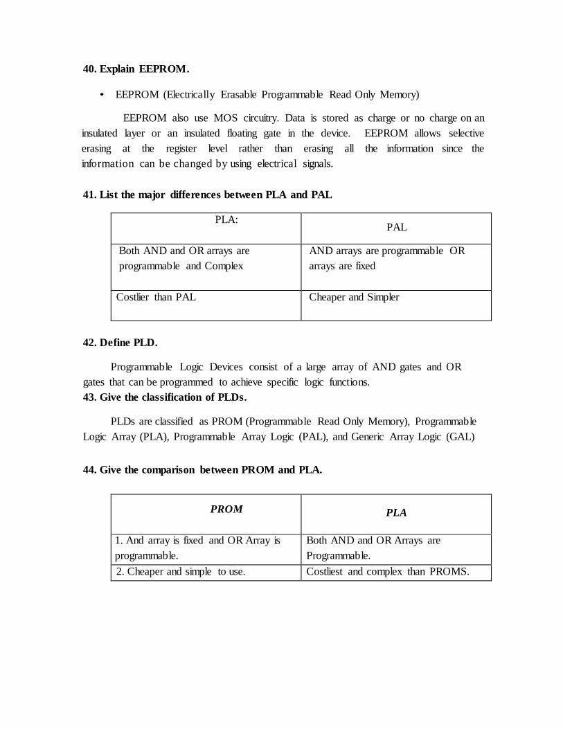
40. Explain EEPROM.
• EEPROM (Electrically Erasable Programmable Read Only Memory)
EEPROM also use MOS circuitry. Data is stored as charge or no charge on an
insulated layer or an insulated floating gate in the device. EEPROM allows selective
erasing at the register level rather than erasing all the information since the
information can be changed by using electrical signals.
41. List the major differences between PLA and PAL
PLA:
PAL
Both AND and OR arrays are
programmable and Complex
AND arrays are programmable OR
arrays are fixed
Costlier than PAL
Cheaper and Simpler
42. Define PLD.
Programmable Logic Devices consist of a large array of AND gates and OR
gates that can be programmed to achieve specific logic functions.
43. Give the classification of PLDs.
PLDs are classified as PROM (Programmable Read Only Memory), Programmable
Logic Array (PLA), Programmable Array Logic (PAL), and Generic Array Logic (GAL)
44. Give the comparison between PROM and PLA.
PROM
PLA
1. And array is fixed and OR Array is
programmable.
Both AND and OR Arrays are
Programmable.
2. Cheaper and simple to use. Costliest and complex than PROMS.
PART B
1. Implement the following function using PLA.
A (x, y, z) =Σm (1, 2, 4, 6)
B (x, y, z) =Σm (0, 1, 6, 7)
C (x, y, z) =Σm (2, 6)
Simplify all the expression using Karnaugh map
Draw the PLA table containing all the minterms
From the PLA table draw the logic diagram of the function
2. Implement the following function using PAL.
W (A, B, C, D) =Σm (2, 12, 13)
X (A, B, C, D) =Σm (7, 8, 9, 10, 11, 12, 13, 14, 15)
Y (A, B, C, D) =Σm (0, 2, 3, 4, 5, 6, 7, 8, 10, 11, 15)
Z (A, B, C, D) =Σm (1, 2, 8, 12, 13)
Simplify all the expression using Karnaugh map
Draw the PAL table containing all the minterms
From the PAL table draw the logic diagram of the function
3. Implement the given function using multiplexer F(A,B,C,D)=∑(1,3,5,6)
Draw the truth table of the given function
Convert the truth table as Implementation table
Select the required type of multiplexer.
Multiplexer Implementation
4. Explain about Encoder and Decoder?
Define the encoder and decoder
Draw the truth table of encoder and decoder
Draw the Logic Diagram of encoder and decoder
Types of encoder
Applications of encoder and decoder
6. Explain in detail about PLA and PAL.
Logic difference between PROM & PLA
Logic diagram implementing a function
Logic difference between PROM & PAL
Logic diagram implementing a function
8. Implement F(A,B,C,D)= (1,3,4,11,12,13,14,15) using multiplexer.
Draw the truth table of the given function
Convert the truth table as Implementation table
Select the required type of multiplexer.
Multiplexer Implementation
9. Implement W(A,B,C,D) = Σ (2,12,13)
X(A,B,C,D) = Σ (7,8,9,10,11,12,13,14,15)
Y(A,B,C,D) = Σ(0,2,3,4,5,6,7,8,10,11,15)
Z (A,B,C,D) = Σ (1,2,8,12,13) using PAL
Simplify all the expression using Karnaugh map
Draw the PAL table containing all the minterms
From the PAL table draw the logic diagram of the function
Unit – IV
Synchronous Sequential Logic
Part - A
1. What is sequential circuit?
Sequential circuit is a broad category of digital circuit whose logic states depend on
a specified time sequence. A sequential circuit consists of a combinational circuit to which
memory elements are connected to form a feedback path.
2. List the classifications of sequential circuit.
i) Synchronous sequential circuit.
ii) Asynchronous sequential circuit.
3. What is Synchronous sequential circuit?
A Synchronous sequential circuit is a system whose behavior can be defined from
the knowledge of its signal at discrete instants of time.
4. What is a clocked sequential circuit?
Synchronous sequential circuit that use clock pulses in the inputs of memory
elements are called clocked sequential circuit. One advantage as that they don‟t cause
instability problems.
5. What is called latch?
Latch is a simple memory element, which consists of a pair of logic gates with their
inputs and outputs inter connected in a feedback arrangement, which permits a single bit to
be stored.
6. List different types of flip-flops.
i) SR flip-flop
ii) Clocked RS flip-flop
iii) D flip-flop
iv) T flip-flop
v) JK flip-flop
vi) JK master slave flip-flop
7. What do you mean by triggering of flip-flop.
The state of a flip-flop is switched by a momentary change in the input signal. This
momentary change is called a trigger and the transition it causes is said to trigger the flip-
flop
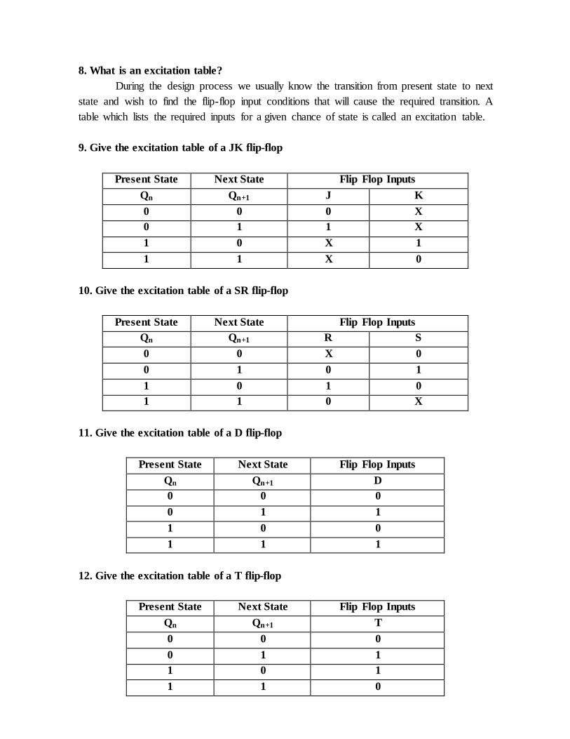
8. What is an excitation table?
During the design process we usually know the transition from present state to next
state and wish to find the flip-flop input conditions that will cause the required transition. A
table which lists the required inputs for a given chance of state is called an excitation table.
9. Give the excitation table of a JK flip-flop
Present State Next State Flip Flop Inputs
Qn Qn+1 J K
0 0 0 X
0 1 1 X
1 0 X 1
1 1 X 0
10. Give the excitation table of a SR flip-flop
Present State Next State Flip Flop Inputs
Qn Qn+1 R S
0 0 X 0
0 1 0 1
1 0 1 0
1 1 0 X
11. Give the excitation table of a D flip-flop
Present State Next State Flip Flop Inputs
Qn Qn+1 D
0 0 0
0 1 1
1 0 0
1 1 1
12. Give the excitation table of a T flip-flop
Present State Next State Flip Flop Inputs
Qn Qn+1 T
0 0 0
0 1 1
1 0 1
1 1 0
13. What is a characteristic table?
A characteristic table defines the logical property of the flip-flop and completely
characteristic its operation.
14. Give the characteristic equation of a SR flip-flop.
Q(t+1)=S+R‟Q
15. Give the characteristic equation of a D flip-flop.
Q(t+1)=D
16. Give the characteristic equation of a JK flip-flop.
Q(t+1)=JQ‟+K‟Q
17. Give the characteristic equation of a T flip-flop.
Q(t+1)=TQ‟+T‟Q
18. What is the difference between truth table and excitation table?
i) An excitation table is a table that lists the required inputs for a given change of state.
ii) A truth table is a table indicating the output of a logic circuit for various input states.
19. What is counter?
A counter is used to count pulse and give the output in binary form.
20. What is synchronous counter?
In a synchronous counter, the clock pulse is applied simultaneously to all flip-flops.
The output of the flip-flops change state at the same instant. The speed of operation is high
compared to an asynchronous counter
21. What is Asynchronous counter?
In a Asynchronous counter, the clock pulse is applied to the first flip-flops. The
change of state in the output of this flip-flop serves as a clock pulse to the next flip-flop and
so on. Here all the flip-flops do not change state at the same instant and hence speed is less.
22. What is the difference between synchronous and asynchronous counter?
Synchronous counter
1. Clock pulse is applied simultaneously Clock pulse is applied to the first flip-flop, the
change of output is given as clock to next flip-flop.
2. Speed of operation is low.
Asynchronous counter
1. Clock pulse is applied to the first flip-flop, the change of output is given as clock to
next flip-flop
2. Speed of operation is high.
23. Name the different types of counter.
a) Synchronous counter
b) Asynchronous counter
i) Up counter
ii) Down counter
iii) Modulo – N counter
iv) Up/Down counter
24. What is up counter?
A counter that increments the output by one binary number each time a clock pulse
is applied.
25. What is down counter?
A counter that decrements the output by one binary number each time a clock pulse
is applied.
26. What is up/down counter?
A counter, which is capable of operating as an up counter or down counter,
depending on a control lead.
27. What is a ripple counter?
A ripple counter is nothing but an asynchronous counter, in which the output of the
flip-flop changes state like a ripple in water.
28. What are the uses of a counter?
i) The digital clock
ii) Auto parking control
iii) Parallel to serial data conversion.
29. What is meant by modulus of a counter?
By the term modulus of a counter we say it is the number of states through which a
counter can progress.
30. What is meant by natural count of a counter?
By the term natural count of a counter we say that the maximum number of states
through which a counter can progress.
31. The number of flip-flops required for modulo-18 counter is---- ---
Ans: n2 T. Therefore 5 flip flops required.
32. What is a ring counter?
A counter formed by circulating a „bit‟ in a shift register whose serial output has
been connected to its serial input.
33. What is BCD counter?
A BCD counter counts in binary coded decimal from0000 to 1001 and back to0000.
Because of the return to0000 after a count of 1001, a BCD counter does not have a regular
pattern as in a straight binary counter.
34. What is a register?
Memory elements capable of storing one binary word. It consists of a group of flip-
flops, which store the binary information.
35. What is a shift register?
In digital circuits, data are needed to be moved into a register (shift in) or moved
out of a register (shift out). A group of flip-flops having either or both of these facilities is
called a shift register.
36. What is serial shifting?
In a shift register, if the data is moved 1 bit at a time in a serial fashion, then the
technique is called serial shifting.
37. Define state of sequential circuit?
The binary information stored in the memory elements at any given time defines the
“state” of sequential circuits.
38. Define state diagram.
A graphical representation of a state table is called a state diagram.
39. What is the use of state diagram?
i) Behavior of a state machine can be analyzed rapidly.
ii) It can be used to design a machine from a set of specification.
40. What is state table?
A table, which consists time sequence of inputs, outputs and flip-flop states, is
called state table. Generally it consists of three section present state, next state and output.
41. What are the different types of shift type?
There are five types. They are,
Serial In Serial Out Shift Register
Serial In Parallel Out Shift Register
Parallel In Serial Out Shift Register
Parallel In Parallel Out Shift Register
Bidirectional Shift Register
42. Give the comparison between combinational circuits and sequential circuits.
Combinational circuits Sequential circuits
Memory unit is not required Memory unity is required
Parallel adder is a combinational
circuit
Serial adder is a sequential circuit
PART B
1. Design a counter with the following repeated binary sequence:0, 1, 2, 3, 4, 5, 6. Use
JK Flip-flop.
Draw the State diagram from the given specifications
Draw the Excitation State table from state diagram
Using K‟Map, Simplify the output and state equation
Draw the Logic diagram of the obtained Boolean function
2. Describe the operation of SR flip-flop
Draw the Logic Diagram of SR flip flop
Draw the Graphical Symbol of SR flip flop
Draw the Characteristics table of SR flip flop
Write the Characteristics equation of SR flip flop
Explain the function of SR flip flop
3. The count has a repeated sequence of six states, with flip flops B and C repeating the
binary count 00, 01, 10 while flip flop A alternates between 0 and 1 every three counts.
Designs with JK flip-flop
Draw the State diagram from the given specifications
Draw the Excitation State table from state diagram
Using K‟Map, Simplify the output and state equation
Draw the Logic diagram of the obtained Boolean function
4. Design a 3-bit T flip-flop counter
Draw the State diagram from the given specifications
Draw the Excitation State table from state diagram
Using K‟Map, Simplify the output and state equation
Draw the Logic diagram of the obtained Boolean function
5. Explain the working of BCD Ripple Counter with the help of state diagram and
logic diagram.
BCD Ripple Counter Count sequence
Truth Table
State diagram representing the Truth Table
Truth Table for the J-K Flip Flop
Logic Diagram
6. Design a sequential detector which produces an output 1 every time the input
sequence 1011 is detected.
Construct state diagram
Obtain the flow table
Obtain the flow table & output table
Transition table Select flip flop Excitation table Logic diagram
7. Explain in detail about serial in serial out shift register.
Block diagram Theoretical explanation
Logic diagram
Working principle
Unit – V
Asynchronous Sequential Logic
Part - A
1. What is flow table?
During the design of asynchronous sequential circuits, it is more convenient to name
the states by letter symbols without making specific reference to their binary values. Such
table is called Flow table.
2. What is primitive flow table?
A flow table is called Primitive flow table because it has only one stable state in
each row.
3. Define race condition.
A race condition is said to exist in asynchronous sequential circuit when two or
more binary state variables change, the race is called non-critical race.
4. Define critical & non-critical race with example.
The final stable state that the circuit reaches does not depend on the order in which
the state variables change, the race is called non-critical race. The final stable state that the
circuit reaches depends on the order in which the state variables change, the race is called
critical race.
5. How can a race be avoided?
Races can be avoided by directing the circuit through intermediate unstable states
with a unique state – variable change.
6. Define cycle and merging?
When a circuit goes through a unique sequence of unstable states, it is said to have a
cycle. The grouping of stable states from separate rows into one common row is called
merging.
7. Give state – reduction procedure.
The state – reduction procedure for completely specified state tables is based on the
algorithm that two states in a state table can be combined in to one if they can be shown to
be equivalent.
8. Define hazards.
Hazards are unwanted switching transients that may appear at the output of a circuit
because different paths exhibit different propagation delays.
9. Does Hazard occur in sequential circuit? If so what is the problem caused?
Yes, Hazards occur in sequential circuit that is Asynchronous sequential circuit. It
may result in a transition to a wrong state.
10. Give the procedural steps for determining the compatibles used for the purpose of
merging a flow table.
The purpose that must be applied in order to find a suitable group of compatibles
for the purpose of merging a flow table can be divided into 3 procedural steps.
i. Determine all compatible pairs by using the implication table.
ii. Find the maximal compatibles using a Merger diagram
iii. Find a minimal collection of compatibles that covers all the states and is closed.
11. What are the types of hazards?
The 3 1) Static – 0 hazards
2) Static – 1 hazard
3) Dynamic hazards
12. What is mealy and Moore circuit?
Mealy circuit is a network where the output is a function of both present state and
input. Moore circuit is a network where the output is function of only present state.
13. Differentiate Moore circuit and Mealy circuit?
Moore circuit
Mealy circuit
a. It is output is a function of present state
only.
a. It is output is a function of present state as
well as the present input.
b. Input changes do not affect the output. b. Input changes may affect the output of the
circuit.
c. Moore circuit requires more number of
states for implementing same function.
c. It requires less numbers of states for
implementing same function.
14. How can the hazards in combinational circuit be removed?
Hazards in the combinational circuits can be removed by covering any two min
terms that may produce a hazard with a product term common to both. The removal of
hazards requires the addition of redundant gates to the circuit.
15. How does an essential hazard occur?
An essential hazard occurs due to unequal delays along two or more paths that
originate from the same input. An excessive delay through an inverter circuit in comparison
to the delay associated with the feedback path causes essential hazard.
16. What is Timing diagram?
Timing diagrams are frequently used in the analysis of sequential network. These
diagrams show various signals in the network as a function of time.
17. What is setup and hold time?
The definite time in which the input must be maintained at a constant value prior to
the application of the pulse is setup time. The definite time is which the input must not
change after the application of the positive or negative going transition of the pulse based
on the triggering of the pulse.
18. Define equivalent state.
If a state machine is started from either of two states and identical output sequences
are generated from every possible set of sequences, then the two states are said to be
equivalent.
19. What is gate delay?
If the change in output is delayed by a time ε with respect to the input. We say that
the gate has a propagation delay of ε. normally propagation delay for 0 to 1 output (ε1) may
be different than the delay for 1 to 0 changes (ε2).
20. Define state reduction algorithm.
State reduction algorithm is stated as “Two states are said to be equivalent if, for
each member of the set of inputs they give the same output and send the circuit either to the
same state or to an equivalent state. When two states are equivalent, one of them can be
removed without altering the input-output relation.
21. What is meant by level triggering?
In level triggering the output of the flip-flop changes state or responds only when the
clock pulse is present.
22. What are the problems involved in asynchronous circuits?
The asynchronous sequential circuits have three problems namely,
a. Cycles
b. Races
c. Hazards
23. Give t h e c o mp a r i s o n b e t w e e n s y n c h r o n o u s & s y n c h ro n o u s
s e q u e n t i a l circuits?
Synchronous sequential circuits Asynchronous sequential circuits.
Memory elements are clocked flip-
Flops
Memory elements are either unlocked
flip - flops or time delay elements.
Easier to design More difficult to design
24. What is fundamental mode sequential circuit?
input variables changes if the circuit is stable
inputs are levels, not pulses
only one input can change at a given time
25. What is pulse mode circuit?
inputs are pulses
widths of pulses are long for circuit to respond to the input
pulse width must not be so long that it is still present after the
new state is reached
26. What is the significance of state assignment?
In synchronous circuits-state assignments are made with the objective of
circuit reduction. Asynchronous circuits- its objective is to avoid critical races
27. What is SM chart?
Just as flow charts are useful in software design, flow charts are useful in the
hardware design of digital systems. These flow charts are called as State Machine Flow
Charts or SM charts. SM charts are also called as ASMC (Algorithmic State machine chart).
ASM chart describes the sequential operation in a digital system.
28. What are the three principal components of SM charts?
The 3 principal components of SM charts are state box, decision box & Conditional
output box.
29. What is decision box?
A diamond shaped symbol with true or false branches represents a decision box. The
condition placed in the box is a Boolean expression that is evaluated to determine which
branch to take in SM chart.
30. What is link path? How many entrance paths & exit paths are there in SM block?
A path through an SM block from entrance to exit is referred to as link path.
An SM block has one entrance and exit path.
31. Differentiate ASM chart and conventional flow chart?
A conventional Flow chart describes the sequence of procedural steps and decision
paths for an algorithm without concern for their time relationship. The ASM chart describes
the sequence of events as well as the timing relationships between the states of a sequential
controller and the events that occur while going from one state to the next.
PART B
1. Design an Asynchronous sequential circuit using SR latch with two inputs A and B and
one output y. B is the control input which, when equal to 1, transfers the input A to
output y. when B is 0, the output does not change, for any change in input.
State Table
Primitive Flow Table
Formal Reduction (Implication Method)
Merging
Reduced Table
K‟Map Simplification
Logic Diagram
2. Give hazard free relation for the following Boolean function.
F (A, B, C, D) =Σm (0, 2, 6, 7, 8, 10, 12)
K‟Map simplification
Create Hazard free link
3. Explain about Hazards?
Explain Static Hazard
Explain Dynamic Hazard
4. Explain about Races?
Explain Critical Race
Explain Non-Critical Race
5. Design T Flip flop from Asynchronous Sequential circuit?
State Table
Primitive Flow Table
Formal Reduction (Implication Method)
Merging
Reduced Table
K‟Map Simplification
Logic Diagram
6. Explain with neat diagram the different hazards and the way to eliminate them.
Classification of hazards
Static hazard & Dynamic hazard definitions
K map for selected functions Method of elimination Essential hazards
7. State with a neat example the method for the minimization of primitive flow
table.
Consider a state diagram
Obtain the flow table
Using implication table reduce the flow table Using merger graph obtain maximal
compatibles Verify closed & covered conditions
Plot the reduced flow table
8. Design a asynchronous sequential circuit with 2 inputs T and C. The output
attains a value of 1 when T = 1 & c moves from 1 to 0. Otherwise the output is 0.
Obtain the state diagram
Obtain the flow table
Using implication table reduce the flow table Using merger graph obtain maximal
compatibles Verify closed & covered conditions
Plot the reduced flow table
Obtain transition table
Excitation table
Logic diagram
9. Explain in detail about Races.
Basics of races
Problem created due to races
Classification of races Remedy for races cycles
10. Explain the different methods of state assignment
Three row state assignment Shared row state assignment
Four row flow table
Multiple row state assignment
Prevention of races.
ADDITIONAL QUESTIONS
Unit – I Boolean algebra and Logic Gates
Part A
1. Find the hexadecimal equivalent of the decimal number 256.
2. Find the octal equivalent of the decimal number 64.
3. What is meant by weighted and non-weighted coding?
4. Convert A3BH and 2F3H into binary and octal respectively.
1. Find the decimal equivalent of (123)9.
2. Find the octal equivalent of the hexadecimal number ABC.D
3. Encode the ten decimal digits in the 2 out of 5 code.
4. Show that the Excess – 3 code is self –complementing.
5. Find the hexadecimal equivalent of the octal number 153.4.
6. Find the decimal equivalent of (346)7.
7. A hexadecimal counter capable of counting up to at least (10,000)10 is to be
constructed.What is the minimum number of hexadecimal digits that the counter must have?
8. Convert the decimal number 214 to hexadecimal.
9. Convert 231.3 4 to base 7.
10. Give an example of a switching function that contains only cyclic prime implicant.
11. Give an example of a switching function that for which the MSP from is not unique.
12. Express x+yz as the sum of minterms.
13. What is prime implicant?
14. Find the value of X = A B C (A+D) if A=0; B=1; C=1 and D=1.
15. What are „minterms‟ and „maxterms‟?
16. State and prove Demorgan‟s theorem.
17. Find the complement of x+yz.
18. Define the following: minterm and term.
19. State and prove Consensus theorem.
20. What theorem is used when two terms in adjacent squares of K map are combined?
21. How will you use a 4 input NAND gate as a 2 input NAND gate?
22. How will you use a 4 input NOR gate as a 2 input NOR gate?
23. Show that the NAND connection is not associative.
24. What happens when all the gates is a two level AND-OR gate network are replaced
by NOR gates?
25. What is meant by multilevel gates networks?
26. Show that the NAND gate is a universal building block.
27. Show that a positive logic NAND gate is the same as a negative logic NOT gate.
28. Distinguish between positive logic and negative logic.
29. Implement AND gate and OR gate using NAND gate.
30. What is the exact number of bytes in a system that contains (a) 32K byte, (b) 64M
bytes, and (c) 6.4G byte?
31. List the truth table of the function: F = x y + x y‟ + y ‟z
Part B
1. (a) Explain how you will construct an (n+1) bit Gray code from an n bit Gray code.
(b) Show that the Excess – 3 code is self –complementing.
2. (a) Prove that (x1+x2).(x1‟. x3‟+x3) (x2‟ + x1.x3) =x1‟x2
(b) Simplify using K-map to obtain a minimum POS expression:
(A‟ + B‟+C+D) (A+B‟+C+D) (A+B+C+D‟) (A+B+C‟+D‟)
(A‟+B+C‟+D‟) (A+B+C‟+D)
3. Reduce the following equation using Quine McClucky method of minimization
F (A,B,C,D) = ∑m(0,1,3,4,5,7,10,13,14,15)
4. (a) State and Prove idempotent laws of Boolean algebra.
(b) using a K-Map ,Find the MSP from of F= ∑(0,4,8,12,3,7,11,15) +∑d(5).
5. (a) With the help of a suitable example, explain the meaning of an redundant
prime implicant.
(b) Using a K-Map, Find the MSP form of F= ∑ (0-3, 12-15) + ∑d (7, 11).
6. (a) Simplify the following using the Quine – McClusky minimization technique
f(a,b,c,d) = ∑ (0,1,2,3,6,7,8,9,14,15).Does Quine –McClusky take care of don‟t
care conditions? In the above problem, will you consider any don‟t care
conditions? Justify your answer.
(b) List also the prime implicants and essential prime implicants for the above case.
7. (a) Determine the MSP and MPS focus of F= ∑ (0, 2, 6, 8, 10, 12, 14, 15).
(b) State and Prove Demorgan‟s theorem
8. Determine the MSP form of the Switching function
F = ∑ ( 0,1,4,5,6,11,14,15,16,17,20- 22,30,32,33,36,37,48,49,52,53,56,63).
9. (a) Determine the MSP form of the Switching function F( a,b,c,d) =∑(0,2,4,6,8) +
∑d(10,11,12,13,14,15).
(b) Find the Minterm expansion of f(a,b,c,d) = a‟(b‟+d) + acd‟.
10. Simplify the following Boolean function by using the Tabulation Method
F= ∑ (0, 1, 2, 8, 10, 11, 14, 15).
11. S ta te and Prove the postulates of Boolean algebra.
12. (a) Find a Min SOP and Min POS for f = b‟c‟d + bcd + acd‟ + a‟b‟c + a‟bc‟d.
13. F ind an expression for the following function usingQuine McCluscky method
F= ∑ (0, 2, 3,5,7,9 ,11,13,14,16,18,24,26,28,30) .
14. S ta te and Prove the theorems of Boolean algebra with illustration.
15. F ind the MSP representation for
F(A,B,C,D,E) = ∑m(1,4,6,10,20,22,24,26) + ∑d (0,11,16,27) using K-Map method.
Draw the circuit of the minimal expression using only NAND gates.
16. (a) Show that if all the gates in a two – level AND-OR gate networks are replaced by
NAND gates the output function does not change.
(b) Why does a good logic designer minimize the use of NOT gates?
17. Simplify the Boolean function F(A,B,C,D) = ∑ m (1,3,7,11,15) + ∑d (0,2,5). If
don‟t care conditions are not taken care, What is the simplified Boolean function?
What are your comments on it? Implement both circuits.
18. (a) Show that if all the gate in a two – level OR-AND gate network are replaced by
NOR gate, the output function does not change.
(b) Implement Y = (A+C) (A+D‟) ( A+B+C‟) using NOR gates only
19. (a) F3 = f(a,b,c,d) = ∑ (2,4,5,6) F2 = f(a,b,c,d) = ∑ (2,3,,6,7)
F1 = f(a,b,c,d) = ∑ (2,5,6,7) .Implement the above Boolean functions.
(i) When each is treated separately and
(ii) When sharing common term
(b) Convert a NOR with an equivalent AND gate.
20. Implement the Switching function whose octal designation is 274 using NAND gates only.
21. Implement the Switching function whose octal designation is 274 using NOR gates only.
22. (a) Show that the NAND operation is not distributive over the AND operation
(b) Find a network of AND and OR gate to realize f(a,b,c,d) = ∑ m (1,5,6,10,13,14) What
is the advantage of using tabulation method?
(c) Determine the prime implicants of the following function using tabulation
method. F( W,X,Y,Z) = ∑(1,4,6,7,8,9,10,11,15)
23. (a) Explain about common postulates used to formulate various algebraic structures.
(b) Given the following Boolean function F= A”C + A‟B + AB‟C + BC Express it in sum
of minterms & Find the minimal SOP expression.
Unit – II Combinational Logic
Part A
1. How will you build a full adder using 2 half adders and an OR gate?
2. Implement the switching function Y= BC‟ + A‟B + D.
3. Draw 4 bit binary parallel adder.
4. Write down the truth table of a full adder.
5. Write down the truth table of a full sub tractor.
6. Write down the truth table of a half sub tractor.
7. Find the syntax errors in the following declarations (note that names for primitive
gates are optional):
module Exmp1-3(A, B, C, D, F)
inputs A,B,C,
output F;
and g1(A,B,D);
not (D,B,A);
OR (F,B,C);
endmodule ;
8. Draw the logic diagram of the digital circuit specified by
module circt (A,B,C,D,F);
input A,B,C,D;
output F;
wire x,y,z,a,d;
and (x,B,C,d);
and (y,a,C);
and (w,z,B);
or (z,y,A);
or (F,x,w);
not (a,A);
not (d,D);
endmodule
9. Define Combinational circuits.
10. Define Half and Full adder.
11. Give the four elementary operations for addition and subtraction.
12. Design the combinational circuit with 3 inputs and 1 output. The output is 1 when
the binary value of the inputs is less than 3.The output is 0 otherwise.
13. Define HDL.
14. What do you mean by carry propagation delay?
15. What is code converter?
16. Give short notes on Logic simulation and Logic synthesis
17. What do you mean by functional and timing simulation?
18. What do you mean by test bench?
19. Give short notes on simulation versus synthesis.
20. Define half sub tractor and full sub tractor.
Part B
1. Design a 4 bit magnitude comparator to compare two 4 bit number.
2. Construct a combinational circuit to convert given binary coded decimal number
into an Excess 3 code for example when the input to the gate is 0110 then the
circuit should generate output as 1001.
3. Design a combinational logic circuit whose outputs are F1 = a‟bc + ab‟c and
F2 = a‟ + b‟c + bc‟.
4. (a) Draw the logic diagram of a *-bit 7483 adder.
(b) Using a single 7483, Draw the logic diagram of a 4 bit adder/sub tractor.
5. (a) Draw a diode ROM, which translates from BCD 8421 to Excess 3 code.
(b) Distinguish between Boolean addition and Binary addition.
6. Realize a BCD to Excess 3 code conversion circuit starting from its truth table.
7. (a) Design a full sub tractor.
(b) How to it differ from a full sub tractor.
8. Design a combinational circuit which accepts 3 bit binary number and converts its
equivalent excess 3 codes.
9. Derive the simplest possible expression for driving segment “a” through „g‟ in an
8421 BCD to seven segment decoder for decimal digits 0 through 9 .Output should
be active high (Decimal 6 should be displayed as 6 and decimal 9 as 9).
10. Write the HDL description of the circuit specified by the following Boolean
function.
(i) Y= (A+B+C) (A‟+B‟+C‟)
(ii) F= (AB‟ + A‟B) (CD‟+C‟D)
(iii) Z = ABC + AB‟ + A(D+B)
(iv) T= [(A+B} {B‟+C‟+D‟)]
11. Design 16 bit adder using 4 7483 ICs
Unit – III Design with MSI Devices
Part A
1. What is a decoder and obtain the relation between the number of inputs „n‟ and
outputs „m‟ of a decoder?
2. Distinguish between a decoder and a demultiplexer.
3. Using a single IC 7485 ; draw the logic diagram of a 4 bit comparator.
4. What is decoder?
5. What do you mean by encoder?
6. Write the short notes on priority encoder.
7. What is multiplexer? Draw the logic diagram of8 to 1 line multiplexer.
8. What do you mean by comparator?
9. Write the HDL description of the circuit specified by the following Boolean
function X=AB+ACD+BC‟.
10. How does ROM retain information?
11. Distinguish between PAL and PLA.
12. Give the classification of memory.
13. What is refreshing? How it is done?
14. What is Hamming code?
15. Write a short note on memory decoding.
16. List the basic types of programmable logic devices.
17. What is PAL? How it differ from PROM and PLA?
18. Write short notes on – PROM, EPROM, EEPROM.
19. How many parity bits are required to form Hamming code if massage bits are 6?
20. How to find the location of parity bits in the Hamming code?
21. Generate the even parity hamming codes for the following binary data.
a. 1101, 1001
22. A seven bit Hamming code is received as 11111101. What is the correct code?
23. Compare static RAMs and dynamic RAMs.
24. Define Priority encoder.
25. Define PLDs.
Part B
1. Implement the switching function F= ∑(0,1,3,4,7) using a 4 input MUX and explain.
2. Explain how will build a 64 input MUX using nine 8 input MUXs.
3. State the advantages of complex MSI devices over SSI gates.
4. Implement the switching function F(A,B,C) = ∑ ( ,2,4,5) using the DEMUX 74156.
5. Implement the switching function F= ∑(0,1,3,4,12,14,15) using an 8 input MUX.
6. Explain how will build a 16 input MUX using only 4 input MUXs.
7. Explain the operation of 4 to 10 line decoder with necessary logic diagram.
8. Draw a neat sketch showing implementation of Z1 = ab‟d‟e + a‟b‟c‟e‟ + bc + de ,
Z2 = a‟c‟e, Z3 = bc +de+c‟d‟e‟+bd and Z4 = a‟c‟e +ce using a 5*8*4 PLA.
9. Implement the switching functions:
Z1 = ab‟d‟e + a‟b‟c‟e‟ + bc + e
Z2 = a‟c‟e,
Z3 = bc +de+c‟d‟e‟+bd and
Z4 = a‟c‟e +ce Using a 5*8*4 PLA
10. Design a switching circuit that converts a 4 bit binary code into a 4 bit Gray code using
ROM array.
11. Design a combinational circuit using a ROM ,that accepts a 3- bit number and generates
an output binary number equal to the square of the given input number.
Unit – IV Synchronous Sequential Logic
Part A
1. Derive the characteristic equation of a D flip flop.
2. Distinguish between combinational and sequential logic circuits.
3. What are the various types of triggering of flip-flops?
4. Derive the characteristic equation of a T flip flop.
5. Derive the characteristic equation of a SR flip flop.
6. What is race round condition? How it is avoided?
7. List the functions of asynchronous inputs.
8. Define Master slave flip flop.
9. Draw the state diagram of „T‟ FF, „D‟ FF.
10. Define Counter.
11. What is the primary disadvantage of an asynchronous counter?
12. How synchronous counters differ from asynchronous counters?
13. Write a short note on counter applications.
14. Compare Moore and Mealy models.
15. When is a counter said to suffer from lock out?
16. What is the minimum number of flip flops needed to build a counter of modulus z 8?
17. State the relative merits of series and parallel counters.
18. What are Mealy and Moore machines?
19. When is a counter said to suffer from lockout?
20. What is the difference between a Mealy machine and a Moore Machines?
21. Distinguish between synchronous and asynchronous sequential logic circuits.
22. Derive the characteristic equation of a JK flip flop.
23. How will you convert a JK flip flop into a D flip flop?
24. What is mean by the term „edge triggered‟?
25. What are the principle differences between synchronous and asynchronous networks?
26. What is lockout? How it is avoided?
27. What is the pulse mode operation of asynchronous sequential logic circuits not very
popular?
28. What are the advantages of shift registers?
29. What are the applications of a shift register?
30. How many flip –flops are needed to build an 8 bit shift register?
31. A shift register comprises of JK flip-flops. How will you complement of the
counters of the register?
32. List the basic types of shift registers in terms of data movement.
33. Write short notes on PRBS generator.
34. Give the HDL dataflow description for T flip – flop.
35. Give the HDL dataflow description for JK flip – flop.
Part B
1. Draw the state diagram and characteristics equation of T FF, D FF and JK FF.
2. (a) What is race around condition? How is it avoided?
(b) Draw the schematic diagram of Master slave JK FF and input and output
waveforms.Discuss how it prevents race around condition.
3. Explain the operation of JK and clocked JK flip-flops with suitable diagrams.
4. Draw the state diagram of a JK flip- flop and D flip – flop.
5. Design and explain the working of a synchronous mod – 3 counter.
6. Design and explain the working of a synchronous mod – 7 counter.
7. Design a synchronous counter with states 0,1, 2,3,0,1 …………. Using JK FF.
8. Using SR flip flops, design a parallel counter which counts in the sequence
a. 000,111,101,110,001,010,000
9. Using JK flip flops, design a parallel counter which counts in the sequence
a. 000,111,101,110,001,010,000
10. ( a) Discuss a decade counter and its working principle.
(b) Draw as asynchronous 4 bit up-down counter and explain its working.
11. (a) How is the design of combinational and sequential logic circuits possible with
PLA?
(b) Mention the two models in a sequential circuit and distinguish between them.
12. D e s ign a modulo 5 synchronous counter using JK FF and implement it.
Construct its timing diagram.
13. A sequential machine has one input line where 0‟s and 1‟s are being incident. The
machine has to produce a output of 1 only when exactly two 0‟s are followed by a
„1‟ or exactly two 1‟s are followed by a „0‟.Using any state assignment and JK
flipflop,synthesize the machine
14. Using D flip –flop ,design a synchronous counter which counts in the sequence
a. 000, 001, 010, 011, 100, 1001,110,111,000
15. U s i n g JK flip-flops, design a synchronous sequential circuit having one and one
output. the output of the circuit is a 1 whenever three consecutive 1‟s are observed.
Otherwise the output is zero.
16. Design a binary counter using T flip – flops to count in the following sequences:
(i) 000,001,010,011,100,101,110,111,000
(ii) 000,100,111,010,011,000
17. (a) Design a synchronous binary counter using T flip – flops.
(b) Derive the state table of a serial binary adder.
18. Design a 3 bit binary Up-Down counter.
19. (i) Summarize the design procedure for synchronous sequential circuit
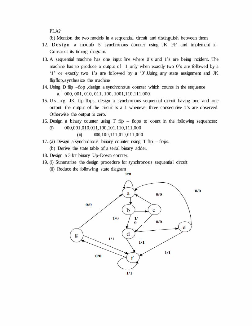
(ii) Reduce the following state diagram
Unit – V Asynchronous Sequential Logic
Part A
1. Distinguish between fundamental mode and pulse mode operation of asynchronous
sequential circuits.
2. What is meant by Race?
3. What is meant by critical race?
4. What is meant by race condition in digital circuit?
5. Define the critical rate and non critical rate.
6. What are races and cycles?
7. What is the significance of state assignment?
8. What are the steps for the analysis of asynchronous sequential circuit?
9. What are the steps for the design of asynchronous sequential circuit?
10. Write short notes on (a) Shared row state assignment.
(b) One hot state assignment.
11. What are Hazards?
12. What is a static 1 hazard?
13. What is a static 0 hazard?
14. What is dynamic hazard?
15. Define static 1 hazard, static 0 hazards, and dynamic hazard.
16. Describe how to detect and eliminate hazards from an asynchronous network.
17. What is static hazard?
18. List the types of hazards.
19. How to eliminate the hazard?
20. Draw the wave forms showing static 1 hazard.
Part B
1. What is the objective of state assignment in asynchronous circuit? Give hazard – free
realization for the following Boolean function f(A,B,C,D) = ∑M(0,2,6,7,8,10,12).
2. Summarize the design procedure for asynchronous sequential circuit. Discuss on
Hazards and races.
3. What do you know on hardware descriptive languages?
4. Design an asynchronous sequential circuit with 2 inputs X and Y and with one
output Z Wherever Y is 1, input X is transferred to Z .When Y is 0; the output does
not change for any change in X.Use SR latch for implementation of the circuit.
5. Develop the state diagram and primitive flow table for a logic system that has 2
inputs x and y and an output z. Reduce primitive flow table. The behavior of the
circuit is stated as follows. Initially x=y=0. Whenever x=1 and y = 0 then z=1,
whenever x = 0 and y = 1 then z = 0.When x=y=0 or x=y=1 no change in z output
remains in the previous state. The logic system has edge triggered inputs without
having a clock. The logic system changes state on the rising edges of the 2 inputs.
Static input values are not to have any effect in changing the Z output .
6. Design an asynchronous sequential circuit with two inputs X and Y and with one
output Z. Whenever Y is 1, input X is transferred to Z.When Y is 0, and the output
does not change for any change in X.
7. Obtain the primitive flow table for an asynchronous circuit that has two inputs x,y
and one output Z. An output z =1 is to occur only during the input state xy = 01 and
then if the only if the input state xy =01 is preceded by the input sequence.
8. A pulse mode asynchronous machine has two inputs. It produces an output whenever
two consecutive pulses occur on one input line only .The output remains at „1‟ until a
pulse has occurred on the other input line. Draw the state table for the machine.
9. (a) How will you minimize the number of rows in the primitive state table of an
incompletely specified sequential machine.
(b) State the restrictions on the pulse width in a pulse mode asynchronous sequential
machine.
10. Construct the state diagram and primitive flow table for an asynchronous network
that has two inputs and one output. The input sequence X1X2 = 00,01,11 causes the
output to become 1.The next input change then causes the output to return to 0. No
other inputs will produce a 1 output.
APPENDIX B
ANNA UNIVERSITY QUESTIONS
B.E./B.Tech. DEGREE EXAMINATION, NOVEMBER/DECEMBER 2009.
Third Semester
(Regulation 2004)
Computer Science and Engineering
CS 1202 - DIGITAL PRINCIPLES AND SYSTEMS DESIGN
(Common to B.Tech. Information Technology)
(Common to B.E. (Part-Time) Second Semester Regulation 2005)
Time: Three hours Maximum: 100 marks
Answer ALL questions.
PART A - (10 x 2 = 20 marks)
1. State and prove De-Morgan's law.
2. Name the various types of number systems with their bases and give an
example for each.
3. What are the advantages of tri-state gates?
4. What is HDL?
5. Distinguish between a decoder and a demultiplexer.
6. How is division operation performed using a subtractor?
7. Give any two applications of a Shift Register.
8. What is Triggering? What is the need for a trigger in a flip-flop?
9. What are Race free assignments?
10. What is a hazard free network?
PART B - (5 x 16 = 80 marks)
11. (a) (i) Use Boolean theorems and simplify the following:
(1) A'BC'+ABC+A'B'C'+A'B'C+AB'C'+A'BC'.
(2) (A + B' +C)(A' +B' +C)(A + B +C)(A' + B +C').
(ii) State and prove the various Boolean Theorems.
Or

(b) Simplify the following expression.
y =m1+m3 +m4+m5+m8+m9+ml0+m11 +m12+ m14 using
(i) Karnaugh map. (8)
(ii) Quine Mcluskey method. (8)
12. (a) What are Universal gates? Represent all the gate operations with
universal gates. (16)
Or
(b) What is a Combinational circuit? Explain with various circuits of
how arithmetic operations are performed. (16)
13. (a) Design a full adder and a full subtract or and implement it with a
suitable decoder. (16)
Or
(b) (i) Explain how HDL is used for combinational circuits. (8)
(ii) Explain the functionality of a multiplexer to get 12 outputs. (8)
14. (a) Design and explain an asynchronous master slave JK-flip-flop and
give its truth table. (16)
Or
(b) Explain how shift registers are useful in performing arithmetic
operations (16)
15. (a) Explain how state reduction in flow tables IS performed using
asynchronous sequential circuits.(16)
Or
(b) Design and explain Fundamental mode and pulse mode sequential
circuits.
B.E./B.Tech. DEGREE EXAMINATION, APRIL/MAY 2008.
Third Semester
(Regulation 2004)
Computer Science and Engineering
CS 1202 - DIGITAL PRINCIPLES AND SYSTEMS DESIGN
(Common to B.Tech. Information Technology)
(Common to B.E. (Part-Time) Second Semester Regulation 2005)
Time: Three hours Maximum: 100 marks
Answer ALL questions.
PART A - (10 x 2 = 20 marks)
1. What are minterms?
2. Convert the following function into sum of product form.
(AB+C)(B+C‟D)
3. Convert the following number from one base to other (65.342)8 = ( )7.
4. What is priority encoder?
5. What is a demultiplexer?
6. Draw the logic diagram of T flip flop.
7. What is the maximum range of a memory that can be accessed by using
10 address lines?
8. What is modulo – N counter?
9. What is a hazard in combinational circuits?
10. What are the assumptions that must be made for fundamental mode
circuit?
PART B - (5 x 16 = 80 marks)
11. (a) Using tabulation method simplify the Boolean function
F (V, W, X, Y, Z) = Σ (0, 1, 8, 11, 12, 15, 20, 21, 22, 24, 29, 31) which
has the don‟t care conditions d (9, 18, 30). (16)
Or
(b) (i) Simplify the Boolean function using map method:
F (w, x, y, z) = Σ (0, 2, 4, 6, 8, 10, 12, 14) (10)
(ii) Perform subtraction on the following numbers using the 9‟s
complement of the subtrahend.
(1) 5763 – 3145
(2) 59 – 9876
(3) 5200 – 561. (6)
12. (a) (i) Design a combinational circuit to convert gray code to BCD. (12)
(ii) What are the design procedures of combinational circuit? (4)
Or
(b) (i) Design a combinational circuit to convert BCD code to excess-3
code. (12)
(ii) Design a 3 bit adder. (4)
13. (a) (i) Implement the Boolean function using 4:1 multiplexer.
F (W, X, Y, Z) = Σ (1, 2, 3, 6, 7, 8, 11, 12, 14) (8)
(ii) A combinational circuit is defined by the functions
F1 = Σ (1, 3, 5)
F2 = Σ (5, 6, 7)
Implement the circuit with a PLA having 3 inputs, 3 product
terms and two outputs. (8)
Or
(b) Construct BCD adder circuit and write a HDL program module for
the same. (16)
14. (a) Explain the different types of shift registers with neat diagram. (16)
Or
(b) Design a sequence detector to detect the sequence 101011. (16)
15. (a) An asynchronous sequential circuit is described by the following
excitation and output function.
X = (Y1Z1‟W2)X + (Y1‟Z1W2‟)
S = X‟
(i) Draw the logic diagram of the circuit.
(ii) Derive the transition table and output map.
(iii) Describe the behavior of the circuit. (16)
Or
(b) Explain essential, static and dynamic hazards in digital circuit. Give
hazard free realization of the following Boolean function.
F (I, J, K, L) = Σm (1, 3, 4, 5, 6, 7, 9, 11, 15) (16)