Embed Size (px)
Citation preview
Appendix A The carrier distribution through a BJT in the active region of operation
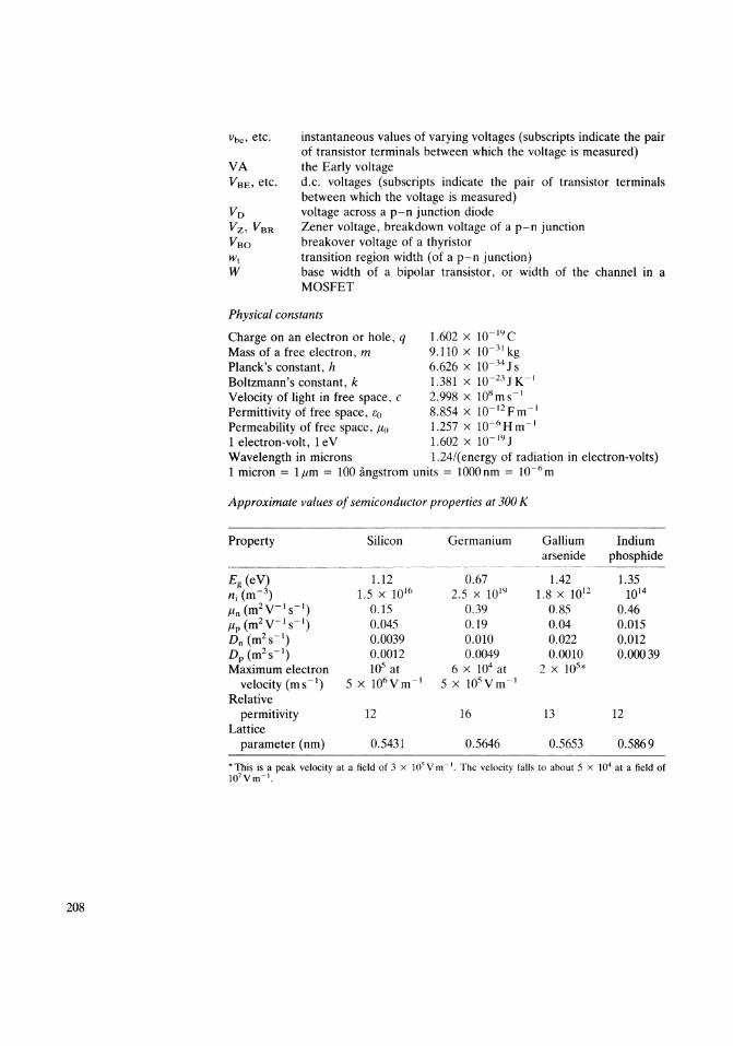
It was explained in Chapter 2 that the minority carrier densities just next to a reverse-biased p-n junction which is carrying a current cannot be as given by Equation 2.28. A reverse bias of -2 V implies a density of about 10-23 m - 3 which could not possibly carry a current of milliamperes. The error in arriving at Equation 2.28 was shown to be due to there being a maximum velocity at which electrons and holes can move, so that at high fields the mobility of electrons and
Emitter-base transition region
Collector-base Emitter I Base Collector region region transition region region ~ ~
10" I I I I
1023 I I I
1022 n-type p·type n-type ~
Relative ' .s 10" current ~ levels ·;;; c -Electrons "' 10" "0 c g 100 (.) 10" "' a; I 0 10 ., 10" /), 0 I
I I 1.0 10" I ...-1
I / I 0.1 10" t/ /)
/1 I x(pm) 10"
0 2 3 4 5 6 7 8 9
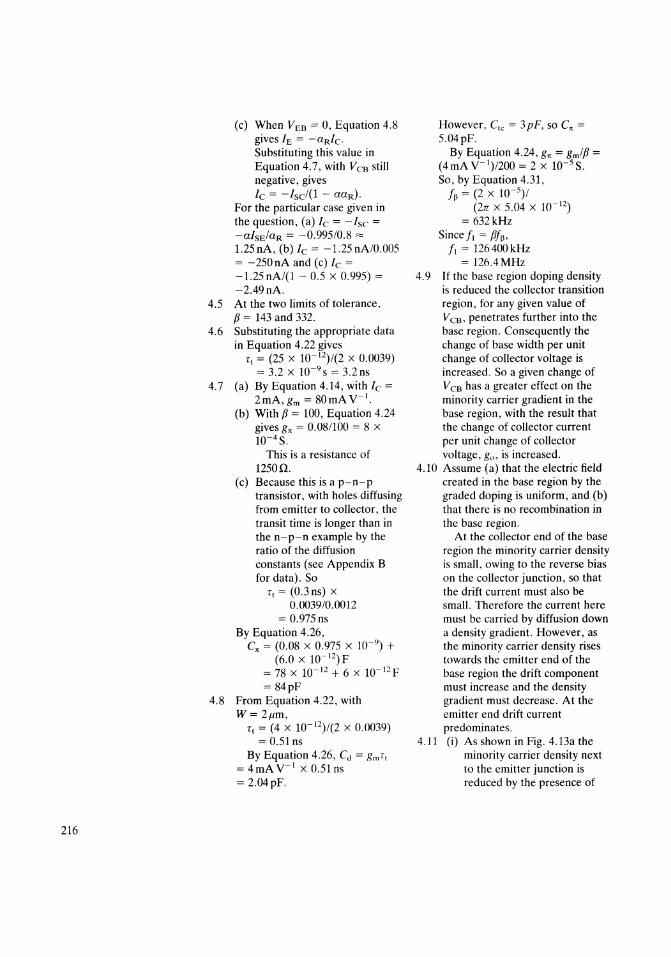
Fig. A.1 Hole and electron distributions for an idealized model of an n-p-n transistor with uniformly doped regions. The collector has a constant reverse bias but the emitter is forward biased to produce four different current levels. Note (a) that the linear minority carrier density gradients in the emitter and base regions appear curved on the log-linear graph and (b) that the electron density at the collector end of the base region is determined by the current level, rather than by the magnitude of the collector-base voltage, as
explained in the text.
205
206
holes can no longer be regarded as a constant in the drift-diffusion equations. This means that towards the collector end of the base region a different kind of solution has to be introduced. That is, when electrons are travelling at about their maximum velocity the electron density is simply proportional to the current flowing. The consequence of this modification to the simple theory presented in Chapter 4 is illustrated by the computed carrier densities in an n-p-n transistor shown Fig. A.l.
In this transistor the emitter donor density is 1024 m-3 , the base acceptor density is uniformly 1021 m - 3 and the collector donor density is 1023 m - 3 . The solid lines show the electron density distributions for four collector currents differing from each other by factors of 10. The actual currents are dependent on the junction area which is not specified, but could refer to milliamperes.
It is worth adding at this point that this finite velocity of carriers through the collector junction of a transistor adds an extra time delay to the base region transit time r1 discussed in Chapter 4. The maximum velocity for electrons in silicon is about 105 m s- 1, so, for a transition region 2 ,urn thick, there will be an extra delay of 0.02ns.
The general conclusion to be drawn from these further comments about the behaviour of p-n junctions is that, as the current density through the junction increases, there is a progressive departure from the condition of space charge neutrality, although for most operating conditions of practical devices, space charge neutrality is a good approximation to use because it leads to quite accurate results even when it is not easy to justify!
Appendix B List of symbols; physical constants and other data
List of symbols for variables
!t, TF, TR
Tn, !p
If/ w a Ct(Ctc, Ctc) cd c,, c~ d E(Ex) g,, g~, go gm hfc
ic, etc.
lc, etc.
/H, lso In, Jp ln, lp L Ln, Lr me, me
M n, n0
Nd, Na p,po Qs, Qss ro, etc. t
normal and reverse common base current gain normal and reverse base-input current gain emitter efficiency permittivity of free space, relative permittivity channel length modulation factor resistivity or charge density conductivity transit time; forward, reverse transit time of transistor minority carrier life times of electrons, of holes contact potential of a p-n junction angular frequency grading factor in a graded p-n junction transition region capacitance (of emitter, collector) diffusion capacitance capacitances in the hybrid 11 equivalent circuit depth of the channel in a MOSFET electric field (in the x direction) conductances in the hybrid 11 equivalent circuit transconductance (and in the hybrid 11 equivalent circuit) small-signal current gain of a BJT instantaneous value of varying current (subscript indicates the transistor terminal through which the current flows) direct currents (subscript indicates the transistor terminal through which the current flows); / 0 also stands for diode current holding current and breakover current in a thyristor current density of electrons, holes length of the n-region, p-region in a BJT length of channel in MOSFET diffusion length of electrons, holes exponent in empirical expression for emitter, collector p-n junction capacitance avalanche multiplication factor electron density, electron density in equilibrium donor, acceptor densities hole density, hole density in equilibrium base charge, saturation base charge small-signal resistances time or oxide thickness in a MOSFET
207
208
instantaneous values of varying voltages (subscripts indicate the pair of transistor terminals between which the voltage is measured) the Early voltage d.c. voltages (subscripts indicate the pair of transistor terminals between which the voltage is measured) voltage across a p-n junction diode Zener voltage, breakdown voltage of a p-n junction breakover voltage of a thyristor transition region width (of a p-n junction) base width of a bipolar transistor, or width of the channel in a MOSFET
Physical constants
Charge on an electron or hole, q Mass of a free electron, m Planck's constant, h Boltzmann's constant, k Velocity of light in free space, c Permittivity of free space, r.0
Permeability of free space, Jlo 1 electron-volt, 1 eV
1.602 X 10- 19 C 9.110 x w-' 1 kg 6.626 x w- 34 J s 1.381 x 10⁻²³ 1 K- 1
2.998 x 10⁸ m s- 1 8.854 X 10- 12 Fm-l 1.257 X 10⁻⁶ Hm- 1 1.602 x w-IY 1
Wavelength in microns 1.24/(energy of radiation in electron-volts) 1 micron = 1 Jim = 100 angstrom units = 1000 nm = 10-6m
Approximate values of semiconductor properties at 300 K
Property Silicon Germanium Gallium Indium arsenide phosphide
------~-~ ---- -· ------ -- - ---- --- --- ---
Eg (eV) 1.12 0.67 1.42 1.35 ni (m-3) 1.5 X 10¹⁶ 2.5 X 10¹⁹ 1.8 X 10¹² 1014 Jin (mzv-1 s-1) 0.15 0.39 0.85 0.46 Jip(m2v-ls-l) 0.045 0.19 0.04 0.015 Dn (m2 s- 1) 0.0039 0.010 0.022 0.012 DP (m2 s- 1) 0.0012 0.0049 0.0010 0.00039 Maximum electron 105 at 6 x 10⁴ at 2 X 10⁵*
velocity (ms- 1) 5 x 10⁶ Vm- 1 5 x to5 vm- 1
Relative permitivity 12 16 13 12
Lattice parameter ( nm) 0.5431 0.5646 0.5653 0.5869
*This is a peak velocity at a field of 3 x 10⁵ V m 1• The velocity falls to about 5 x 10⁴ at a field of to7vm-l
Answers to exercises
1.1 If Tis the temperature rise, then decreases as the temperature 1.5 X 1016 X (1.08)T rises.
= 2.5 X 10 19 1.4 In silicon, n; = 1.5 x 10¹⁶ m -3, So and since Nd = 1020 m-3 it follows
T = 96.4 degrees. thatp0 = 2.25 x 10¹² m-3 .
1.2 Assuming the density of thermally Adapting Equation 1.10 to the generated carriers is negligible case of hole recombination: compared with Nd, n0 = Nd and Pc(O) = 1018 m-3
p0 = n;2INJ. So in germanium, (since p0 is negligible) n0 = 1021 m-3 and Po= 6.25 X and 1017 m- 3. More accurately, let Pc(t) = 2.25 X 10¹² m-3
there be a density C of thermally so generated holes and electrons, so 2.25 X 10-6 = exp(-t/2.0f1S) that p0 = C and n 0 = NJ + C; and then for electrons in germanium, t = 26.0 flS.
. 2 smce n 0p 0 = n; , 1.5 With a forward bias voltage of (NJ + C) X c = 6.25 X 1038 0.2 V, qV0 /kT = 8, so
So, with Nct = 1021 , lo = /sexp8 C =Po = 6.246 X 10 17 In silicon, Is = 10- 13 so
= 6.25 x 10¹⁷ m-3 / 0 = 0.298nA, and in So, even in germanium at 300 K, germanium, with this doping density, the Is= 10-6 so / 0 = 2.98mA. density of thermally generated The silicon diode remains carriers is negligible. In silicon it virtually cut -off even with a is even more negligible: with forward bias of 0.2 V. (However, no= 1021 what counts as cut-off depends on
p 0 = 2.25 x 10¹¹ m- 3 the application.) 1.3 When Po= NJ then 2N/ = n?. 1.6 The slope of the load line is - R
However, NJ = 1021 m-3 , son;= which, in this case, gives 1.41 x 10²¹ m-3. R = (0.4 V)/(2.5 rnA) = 160 Q.
In silicon, n; = 1.5 x 10¹⁶ m-3 at The power delivered to the load is 300 K and dn;ldT = 1.08, so, if T VI = (0.4 V) x (2.5 rnA) =
is the temperature rise, l.OmW. 1.5 X 1016 X (1.08) T The load resistance that draws
= 1.41 X 10²¹ maximum power from the cell, So with the given level of
T = 149 degrees. illumination, is represented by the In germanium, n; = 2.5 x load line that intersects the 1019 m-3 at 300K and dn;ldT = characteristic at the point which 1.05, so T = 82.6 degrees. subtends the largest area Note that both these figures are rectangle within the fourth underestimates because dn;ldT quadrant. In this case the point of
209
210
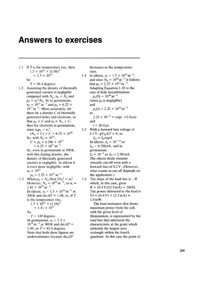
/0 (mAI
0.4 +----+---+-------,1-----+--Vos = 6V
V05 = 1V
-4 -3 -2 -1 0
n-channel JFET
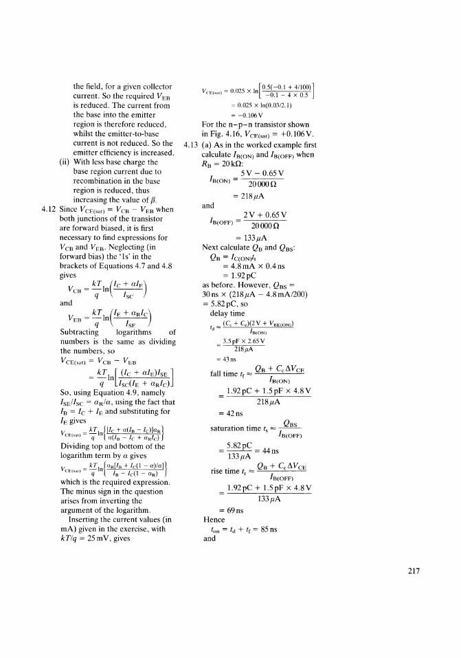
Fig. A.2 Graphs of drain current versus gate voltage for an n-channel JFET. See Exercise 1. 7.
intersection is about 0.505 V and -2.2mA, giving a resistance of 230n and a power output of l.llmW.
1. 7 The required graph is shown in Fig. A.2. The values of transconductance required are the slopes of the two curves at the specified operating points. (a) In the linear region (i.e. when V0 s = 1 Vand Vas> -3V) the value of gm is constant, namely 40 ,uA v- 1• (b) In the saturation region, with Vos = 6 V, gm varies with Vas· When 10 = 0.15mA the slope of the graph gives gm = 100,uA v- 1•
1.8 The slope at point X in Fig. 1.14 is go"" 0.05/10V = 5 X 10⁻⁶, or ro = 200kn. At/0 = 0.24mA and V0 s = 2V, g0 ""0.21 mA/3 V = 7 X 10⁻⁵, or ro = 14kn.
1.9 The net load resistance is 10kn in parallel with 40 kn, namely 8 kn.
SoAv = gmRL = (400,uA v-1) X 8 kil = 3.2. Av(max) = gmro = 16.
1.10 First calculate gm (using Equation 1.20). gm = qlclkT = 40mA y-l X 5 = 200mA y- 1.
Then calculate r" (using Equation 1.21). '" = {Jfgm = 150/200mA v- 1 = 750il. Substituting these values in Equation 1.23 gives
A _ 75on v- 100 + 75on
200mAV- 1
X 5 X 10 5 + 2 X 10 3
= 86 If rb = 0 the first fraction can be ignored and Av = 97.5.
2.1 First calculate the conductivity using Equation 2.7.
a= 1.602 X 10- 19(0.15 X 10²⁰
+ 0.045 X 2.25 X 1012)
The contribution of hole conduction in this case is clearly negligible. So a = 2.4 S m - 1•
Therefore resistivity p = have yet to become economically 0.417Qm. viable.
2.2 Using Equation 2.23 for the 2.4 The equation for Is can be silicon p-n junction, derived from Equations 2.31 and
exp(qlfl/kT) 2.26. At 300 K, in the n-region = (2.25 X 1032)/1044 withNct = l023 m-3,p0 o2.25 X
so 109, so the hole current is qljllkT = -26.8 proportional to DpPnolln =
0.0012 X 2.25 X 109/20 X 10-6 = so if qlkT = 40 v- 1 1.35 x 10¹¹ .
If/= -0.671 v Similarly, in the p-region with For the germanium junction, Na = l022 m-3 , npo = 2.25 X
exp(qlfllkT) 1010 m - 3 , so the electron current = ( 6.25 X 1038)/1044 is proportional to Dnnp(/lp =
so 0.0039 X 2.25 X 1010/20 X 10-6 = qlfllkT = -12.0 43.9 X 10¹¹ .
1f1 = -0.3V The more heavily doped n-type 2.3 A forward current does not region has producted the greater
produce a refrigerating effect, contribution to the current. even though the current is flowing Is is the sum of these two up an electrical potential gradient quantities multiplied by A X q, so in the transition region, because Is= (10-8 m2)(1.6 X 10⁻¹⁹ C) X
any energy absorbed by carriers (1.35 + 43.9) X 1011 = 7.24 X
climbing the potential barrier is w-ls A. balanced by the energy dissipated 2.5 Since the diode is significantly by the diffusion process. forward biased, the '-1' in Refrigeration can, however, occur Equation 2.26 can neglected. So if when large reverse currents can I0 = Isexp(qV0 /kT), then be made to flow through junctions 10I0 = fsexp[q(V0 + ~Vo)lkT] in which there is a high where ~ V 0 is the extra voltage generation-recombination rate. needed to produce a 10-fold Thus, when a reverse current increase in the current I0 .
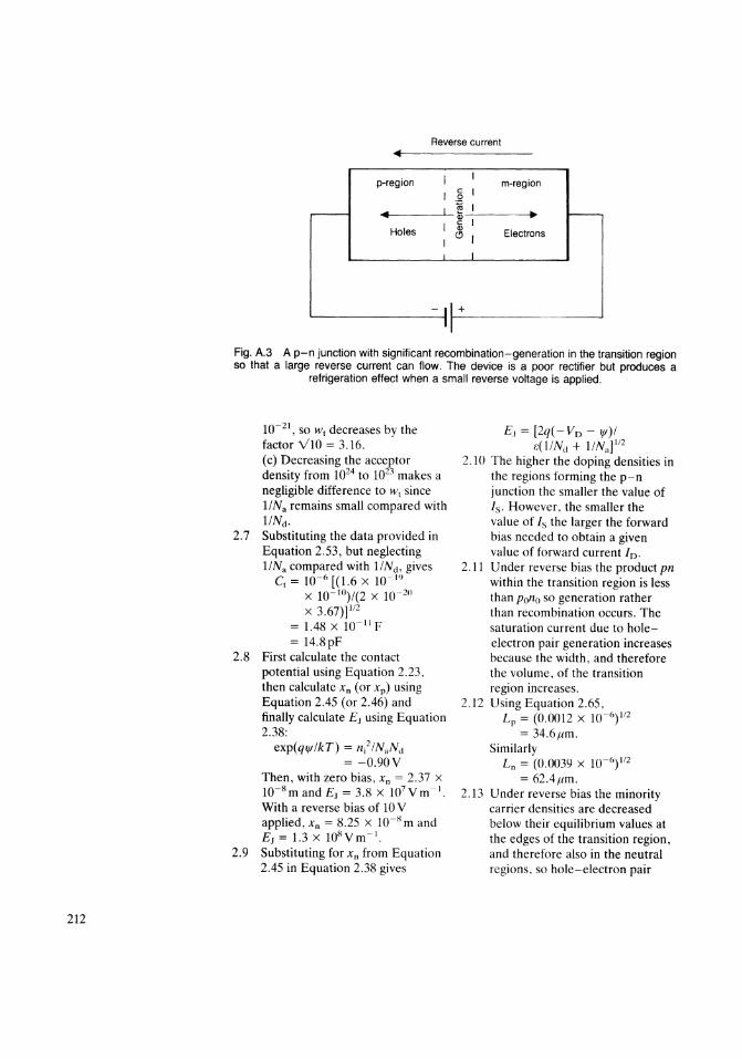
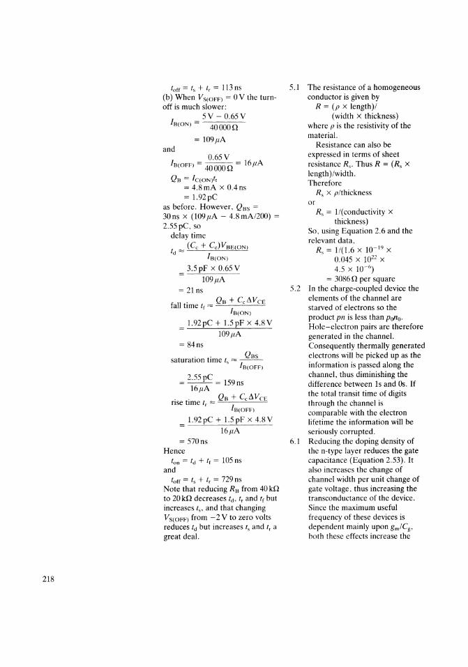
flows, holes and electrons leave Dividing one of these equations the transition region, as shown in by the other gives Fig. A.3, implying that hole- 10 = exp(q ~ V0 /kT) electron pair generation must be = exp(40V- 1 X ~Vo) occurring there. However, every So time a hole-electron pair is ~V0 = 57.5mV. created an energy, Eg (eV), must 2.6 This exercise demonstrates the be taken out of the surrounding dependence of w1 on various environment, cooling it down and variables. producing a refrigerating effect. (a) Increasing the reverse bias to Evidently then, refrigerating 10 V increases w1 by the factor junctions must be poor rectifiers. (10.67/3.67)112 = 1.705. Normal silicon p-n junctions do (b) In the expression 1/Na + liNd not make good refrigerating the more lightly doped region devices. Other semiconducting dominates. In this case increasing materials are to be preferred, but, N ct from 1020 to 1021 still leaves as solid state refrigerators, they l!Na negligible compared with
211
212
Reverse current
p-region t: 0
m-region
e __... ~~-H-ol-es---J-~-:----E-1-ec-t:•ons -
I
Fig. A.3 A p-n junction with significant recombination-generation in the transition region so that a large reverse current can flow. The device is a poor rectifier but produces a
refrigeration effect when a small reverse voltage is applied.
10-21 , SO W1 decreases by the factor v'10 = 3.16. (c) Decreasing the acceptor density from 1024 to 1023 makes a negligible difference to w1 since liN. remains small compared with liN ct.
2.7 Substituting the data provided in Equation 2.53, but neglecting liN. compared with 1/Nd, gives
C1 = 10-6 [(1.6 x 10- 19
x 10-10)/(2 x 10-20
X 3.67)]112
= 1.48 X 10- 11 F = 14.8pF
2.8 First calculate the contact potential using Equation 2.23, then calculate Xn (or xp) using Equation 2.45 (or 2.46) and finally calculate E1 using Equation 2.38:
exp(ql/flkT) = n?IN.Nd = -0.90V
Then, with zero bias, Xn = 2.37 x 10⁻⁸ mand£1 = 3.8 X 10⁷ Vm- 1.
With a reverse bias of 10 V applied, Xn = 8.25 X 10⁻⁸ m and E1 = 1.3 X 10⁸ Vm- 1•
2.9 Substituting for Xn from Equation 2.45 in Equation 2.38 gives
E1 = [2q(-V0 - 'If)/ r.(l!Nd + 11N.P12
2.10 The higher the doping densities in the regions forming the p-n junction the smaller the value of Is. However, the smaller the value of Is the larger the forward bias needed to obtain a given value of forward current / 0 .
2.11 Under reverse bias the product pn within the transition region is less than p0n0 so generation rather than recombination occurs. The saturation current due to holeelectron pair generation increases because the width, and therefore the volume, of the transition region increases.
2.12 Using Equation 2.65, LP = (0.0012 X 10⁻⁶ ) 112
= 34.6pm. Similarly
Ln = (0.0039 X 10⁻⁶ ) 112
= 62.4pm. 2.13 Under reverse bias the minority
carrier densities are decreased below their equilibrium values at the edges of the transition region, and therefore also in the neutral regions, so hole-electron pair
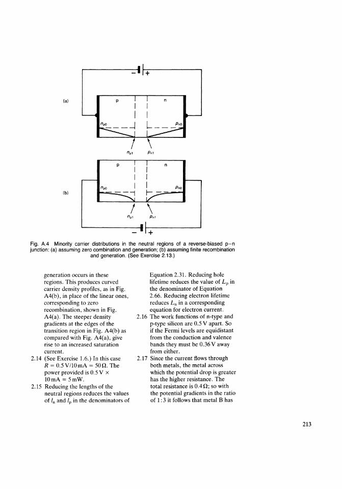
+
(a) p n
n., Pn1
p n
Pn0 (b)
n., Pn1
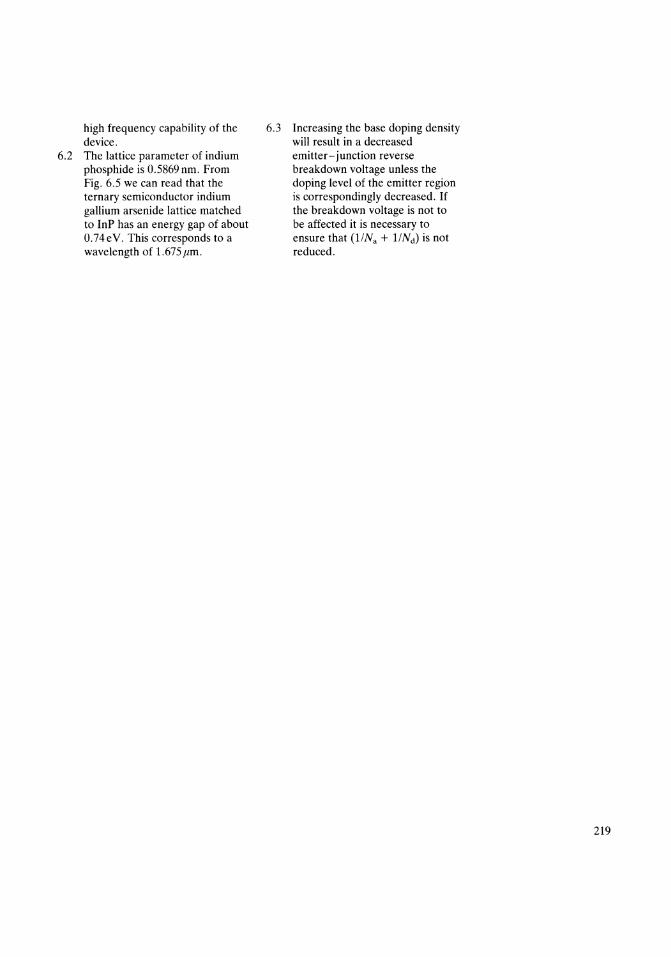
+ Fig. A.4 Minority carrier distributions in the neutral regions of a reverse-biased p-n junction: (a) assuming zero combination and generation; (b) assuming finite recombination
and generation. (See Exercise 2.13.)
generation occurs in these regions. This produces curved carrier density profiles, as in Fig. A4(b), in place of the linear ones, corresponding to zero recombination, shown in Fig. A4(a). The steeper density gradients at the edges of the transition region in Fig. A4(b) as compared with Fig. A4(a), give rise to an increased saturation current.
2.14 (See Exercise 1.6.) In this case R = 0.5V/10mA = 500. The power provided is 0.5 V x lOrnA= 5mW.
2.15 Reducing the lengths of the neutral regions reduces the values of ln and lp in the denominators of
Equation 2.31. Reducing hole lifetime reduces the value of Lp in the denominator of Equation 2.66. Reducing electron lifetime reduces Ln in a corresponding equation for electron current.
2.16 The work functions of n-type and p-type silicon are 0.5 V apart. So if the Fermi levels are equidistant from the conduction and valence bands they must be 0.36 V away from either.
2.17 Since the current flows through both metals, the metal across which the potential drop is greater has the higher resistance. The total resistance is 0.40; so with the potential gradients in the ratio of 1 : 3 it follows that metal B has
213
214
resistance of 0.3 n and metal A has a resistance of 0.1 n.
2.18 Substituting the given values in the diode equation (neglecting the - 1 in the brackets) gives
w-3 A = w-9 A x exp(V0 /0.025V)
or In 106 = V0 /0.025
so V0 = 13.8 X 0.025 = 0.345 V
3.1 From Equation 3.14,
so
lo g = _ __!:.._
0 Vos + 1/}.
0.0075A go= 9V + 40V
= 1.53 x w-4 n- 1
or r o = 6.5 k!l. From Equation 3.12, at pinch-off,
gm = 2loss(1 + Vas) Vp Vp
= 0.4 X 12.5 rnA X (1 - 1/5)
= 4mA v- 1
However, as V os is increased above pinch-off gm increases according to Equation 3.15;
gm lo
gm(at pinch-off) fo(at pinch-off)
Vos + 1/.lc Vp +Vas+ 1/.lc
So, at the stated operating point, gm = 4mA y-l X 49/44 = 4.45 rnA v- 1, and the maximum available voltage gain is gmlg" = o.00445/1.53 x w-4 = 29.
3.2 Consider an n-channel MOSFET with Vos = 0, whose gate is made sufficiently positive for a channel to be created (i.e. Vas> VT)- As V0 s is made more positive a point will be reached at which the drain-gate voltage will become less than VT, so that one might expect that no mobile carriers would be induced into the drain
end of the channel and 10 would be cut off. However, if that were the case there would be no IR voltage drop along the channel and all points along the channel would remain at the source voltage thus ensuring that the channel would not be cut off! This contradiction can only be resolved by the channel becoming 'pinched off leaving just sufficient channel to allow the saturation current to flow as V os is increased further.
3.3 Ann-channel MOSFET with a negative threshold voltage is a depletion mode device. The channel is just pinched off when Vos =Vas- VT, so in this case V os = 5 V; when V os > 5 V the gate is negative with respect to the drain by more than 2 V.
3.4 At any point along the broken line in Fig. 3.8a V05 =Vas- VT. Substituting for Vas - V T in Equation 3.22 gives
lo = PVos212 So, for example, when V0 s = 3V,l0 = 25 X 4.5J1A = 112.5 JLA. This result applies to both graphs. Taking other values of V os confirms that the current axes have linear scales. From the points of intersection between the broken line and the characteristic curves it follows that, for Fig. 3.8a, VT = 2 V, implying an enhancement-mode device. Similarly, for Fig. 3.8b, VT = -3 V, implying a depletion-mode device.
3.5 First calculate Cox from Equation 3.25:
Cox = (8.85 X 10- 12
X 4Fm- 1)/
(0.2 X 10⁻⁶ m) = 1.77 X 10⁻⁴ Fm-2•
Substituting this value in Equation 3.23, when W/L = 3, gives
fJ = 3 X 0.07 X 1.77 X 10-4 However, /E = Ie + JB, so = 37.2pA v-2 (/e + IB)Ile = lla
3.6 The region of silicon just under or the gate, looked at along they 1 + /Bile = 1/a dimension, is simply a portion of However, from Equation 4.2, a transition region in equilibrium. /Bile= 1/fJ; so 1 + 11/3 = 1/a So, according to Equation 2.25, This can be rewritten as the product of the hole and fJ = a/(1 - a) or as electron densities is everywhere a = fJ/(1 + fJ) equal ton?. 4.2 If a = 0.98 then fJ = 0.98/0.02 =
3.7 Figure 3.15 demonstrates that, in 49. Similarly, if a = 0.99 then a p-channel device, donors fJ = 99. increase the magnitude of the 4.3 In an n-p-n transistor fJ is the threshold voltage of an ratio of the emitter-to-base enhancement-mode FET. In an electron current and the base-n-channel MOSFET, therefore, to-emitter hole current. In any donors will bias the threshold given transistor these currents voltage towards depletion mode are proportional to npe and operation. Pne• respectively (by Equations
3.8 The separation between the 4.3 and 4.4, assuming npo and curves in Fig. 3.17, when Vos = Pno are negligible). However, npe 1 V, is about 0.04mA, so gm = and Pne are both proportional 40 pA v-1. When V os = 6 V the to exp(qVBE/kT). So as VBE separation is about 0.1 rnA, so varies, thus varying the collector gm = 100pA v-1• The same current, the value of fJ should results are obtained by not alter. (Note: we will see later calculation. how a more accurate model
In the linear region, where of the behaviour of the base gm = 40pA v-1 when V08 = 1 V, region explains why fJ, in fact, it follows from Equation 3.30 that increases with increasing Ie over fJ = 40,uA v-2 . quite a large range of current
In the saturation region densities.) Equation 3.31 applies. We found 4.4 (a) When JE = 0 and VeB is that when V0 s = 6V and Vas= negative, Ie = - lse, by 4.5V, gm = lOO,uA v-1• So, by Equation 4.7. Equation 3.31, (b) When /B = 0, Ie + /E = 0.
lOO,uA v-1 = f3(4.5V- 2V} (Note that with the Hence fJ = 40pA v- 2 (as before). convention adopted by the
3.9 From Equation 3.32, using the Ebers-Moll equations, in data given and with which forward biasing fJ = 40,uA v- 2 , currents and voltages are
gds = 40,uA y-2 regarded as positive, Ie and x(5V-2V-1V) JE both flow inwards (for
= 80 x w-6 s p-n-p) or outwards (for n-This is to be compared with your p-n), SO JB = JE + Jc). measurement of the slope of the Putting -le in place of JE in graph at the specified operating Equation 4.7, with Ve8 still point in the linear region. negative, gives
4.1 From Equation 4.1, JE//e = 1/a. le = -lsef (1 - a).
215
216
(c) When VEB = 0, Equation 4.8 gives IE = -aRic. Substituting this value in Equation 4.7, with Vc8 still negative, gives Ic = -/5c/(1 - aaR).
For the particular case given in the question, (a) Ic = -lsc = -alsEiaR = -0.995/0.8 = 1.25 nA, (b) /c = -1.25 nA/0.005 = -250nA and (c) Ic = -1.25 nA/(1 - 0.5 X 0.995) = -2.49nA.
4.5 At the two limits of tolerance, fJ = 143 and 332.
4.6 Substituting the appropriate data in Equation 4.22 gives
r1 = (25 X 10- 12)/(2 X 0.0039) = 3.2 X 10⁻⁹ s = 3.2ns
4.7 (a) By Equation 4.14, with lc = 2mA, gm =SOmA v- 1.
(b) With fJ = 100, Equation 4.24 gives g" = 0.08/100 = 8 X
w-4 s. This is a resistance of
1250Q. (c) Because this is a p-n-p
transistor, with holes diffusing from emitter to collector, the transit time is longer than in the n-p-n example by the ratio of the diffusion constants (see Appendix B for data). So
r, = (0.3 ns) x 0.0039/0.0012
= 0.975 ns By Equation 4.26,
Crr = (0.08 X 0.975 X 10- 9) + (6.0 X 10- 12) F
= 78 X 10-12 + 6 X 10- 12 F = 84pF
4.8 From Equation 4.22, with W= 2Jlm,
r, = (4 X 10-12)/(2 X 0.0039) = 0.51 ns
By Equation 4.26, Cct = gm r, = 4mA v- 1 x 0.51 ns = 2.04pF.
However, C~e = 3pF, soC"= 5.04pF.
By Equation 4.24, grr = gmlfl = (4mA v- 1)/200 = 2 x w-ss. So, by Equation 4.31,
/p = (2 x w-5)1 (2n X 5.04 X 10- 12)
=632kHz Since / 1 = {J[p,
/ 1 = 126400kHz = 126.4MHz
4.9 If the base region doping density is reduced the collector transition region, for any given value of V cs. penetrates further into the base region. Consequently the change of base width per unit change of collector voltage is increased. So a given change of V cs has a greater effect on the minority carrier gradient in the base region, with the result that the change of collector current per unit change of collector voltage, g0 , is increased.
4.10 Assume (a) that the electric field created in the base region by the graded doping is uniform, and (b) that there is no recombination in the base region.
At the collector end of the base region the minority carrier density is small, owing to the reverse bias on the collector junction, so that the drift current must also be small. Therefore the current here must be carried by diffusion down a density gradient. However, as the minority carrier density rises towards the emitter end of the base region the drift component must increase and the density gradient must decrease. At the emitter end drift current predominates.
4.11 (i) As shown in Fig. 4.13a the minority carrier density next to the emitter junction is reduced by the presence of
the field, for a given collector current. So the required VEB is reduced. The current from the base into the emitter region is therefore reduced, whilst the emitter-to-base current is not reduced. So the emitter efficiency is increased.
(ii) With less base charge the base region current due to recombination in the base region is reduced, thus increasing the value of p.
4.12 Since VcE(sat) = Vcs- VEB when both junctions of the transistor are forward biased, it is first necessary to find expressions for Vc8 and VEB· Neglecting (in forward bias) the '1s' in the brackets of Equations 4.7 and 4.8 gives
V CB = kT ln(/c + a/E) q fsc
and
VEB = kTln(IE + aR/c) q lsE
Subtracting logarithms of numbers is the same as dividing the numbers, so VcE(sat) = Vcs- VEB
= kTln[ (Ic + a/E)/sE] q lsc(IE + aR/c)
So, using Equation 4.9, namely lsEilsc = aRia, using the fact that / 8 = lc + IE and substituting for IE gives V _ kT1 {[lc + a(la- Jc)]aR}
CE(.at) - q n a(Ia - Ic + aR/c)
Dividing top and bottom of the logarithm term by a gives V _ kT1 {aR[Ia + /c(l -a)/a]}
CE(-.tl - q n Ia Ic(! - aR)
which is the required expression. The minus sign in the question arises from inverting the argument of the logarithm.
Inserting the current values (in rnA) given in the exercise, with kT/q = 25mV, gives
- [0.5( -0.1 + 4/100)] V CE(.at) - 0.025 X In 0.1 4 X 0.5
= 0.025 x ln(0.03/2.1)
= -0.106V For the n-p-n transistor shown in Fig. 4.16, VcE(sat) = +0.106V.
4.13 (a) As in the worked example first calculate Is( ON) and Is( OFF) when R8 = 20kn:
5V- 0.65V /B(ON) = 20000!1
= 218p.A and
2V + 0.65V /B(OFF) = 20000!1
= 133p.A Next calculate Q8 and Qss:
Qs = lqoN)tt = 4.8mA X 0.4ns = 1.92 pC
as before. However, Q8 s = 30 ns x (218 p.A - 4.8 mA/200) = 5.82pC, so
delay time ld = (Cc + Ce)(2V + VBE(ON))
JB(ON)
_ 3.5pF X 2.65V - 218pA
= 43ns
f II . Qs + CcLiVcE a time tr"" 1 B(ON)
1.92 pC + 1.5 pF X 4.8 v 218p.A
= 42ns . . Qss
saturatiOn time t. "" -1-B(OFF) _ 5.82pC _ 44 - 133p.A- ns
. . Qs + CcLiVcE nse time tr "" 1 B(OFF)
_ 1.92pC + 1.5pF X 4.8V - 133p.A
= 69ns Hence
ton = td + tr = 85 ns and
217
toff = t, + tr = 113 ns 5.1 The resistance of a homogeneous (b) When Vs(oFF) = OV the turn- conductor is given by off is much slower: R = (p x length)/
/B(ON) = 5V-0.65V (width x thickness)
40000!1 where p is the resistivity of the
= 109f1A material.
and Resistance can also be
0.65V expressed in terms of sheet /B(OFF) = 40000!1 = 16f1A resistance R,. Thus R = (R. x
Qs = lqoN)tt length)/width. Therefore
= 4.8mA x 0.4ns R, x p/thickness
= 1.92 pC as before. However, Q8 s =
or
30ns x (109f1A- 4.8mA/200) = R, = 1/( conductivity X
2.55pC, so thickness)
delay time So, using Equation 2.6 and the
_ (Cc + Ce)VBE(ON) relevant data,
td- R, = 1/(1.6 x 10-19 x /B(ON) 0.045 X 1022 X
3.5 pF X 0.65 V 4.5 x 10⁻⁶)
109J1A = 3086 n per square
= 21ns 5.2 In the charge-coupled device the
Qs + Cc~VcE elements of the channel are fall time ft =
/B(ON) starved of electrons so the product pn is less than pon0 .
1.92pC + 1.5pF X 4.8V Hole-electron pairs are therefore 109flA generated in the channel.
= 84ns Consequently thermally generated . . Qss electrons will be picked up as the
saturatwn time t, = -1 -- information is passed along the B(OFF)
= 2.55 pC = 159 channel, thus diminishing the
16f1A ns difference between 1s and Os. If
Qs + Cc~VcE the total transit time of digits rise time t, =
/B(OFF) through the channel is comparable with the electron
1.92 pC + 1.5 pF X 4.8 V lifetime the information will be 16f1A seriously corrupted.
= 570ns 6.1 Reducing the doping density of Hence the n-type layer reduces the gate
ton = td + ft = 105 ns capacitance (Equation 2.53). It and also increases the change of
toff = t, + tr = 729ns channel width per unit change of Note that reducing R8 from 40 kn gate voltage, thus increasing the to 20kn decreases td, tr and ft but transconductance of the device. increases t,, and that changing Since the maximum useful Vs(OFF) from -2 V to zero volts frequency of these devices is reduces td but increases t, and tr a dependent mainly upon gm!Cg, great deal. both these effects increase the
218
high frequency capability of the device.
6.2 The lattice parameter of indium phosphide is 0.5869 nm. From Fig. 6.5 we can read that the ternary semiconductor indium gallium arsenide lattice matched to InP has an energy gap of about 0.74eV. This corresponds to a wavelength of 1.675 Jlm.
6.3 Increasing the base doping density will result in a decreased emitter-junction reverse breakdown voltage unless the doping level of the emitter region is correspondingly decreased. If the breakdown voltage is not to be affected it is necessary to ensure that (liN. + l!Nct) is not reduced.
219
220
References
Beaufoy, R. and Sparkes, J.J. (1957) The junction transistor as a charge-controlled device. ATE Journal, 13, 310-27.
Bradley, D. (1987) Power Electronics, Van Nostrand Reinhold, New York. Crecraft, D., Gorham, D. and Sparkes, J.J. (1993) Electronics. Chapman & Hall, London. Early, J.M. (1952) Effect of space charge layer widening in junction transistors. Proceedings
of the IRE, 40, 1401-13. Ebers, J.J. and Moll, J.L. (1954) Large-signal behaviour of junction transistors. Proceedings
of the IRE, 42, 1761-72. Giacoletto, L.J. (1954) Study of pnp alloy junction transistors from de through medium
frequencies. RCA Review, 15, 506-62. Gowar, J. (1984) Optical Communications Systems, Wiley, New York. Hodges, D.A. and Jackson, H. G. (1983) Analysis and Design of Digital Integrated Circuits,
McGraw-Hill, New York. Horowitz, P. and Hill, W. (1980) The Art of Electronics. Cambridge University Press,
Cambridge. Mavor, J., Jack, M.A. and Denyer. P.B. (1983) Introduction to MOS LSI Design, Addison
Wesley, Reading, MA. Millman, J. (1979) Microelectronics, McGraw-Hill, New York. Nagel, N.W. (1975) SPICE2, a computer program to simulate semiconductor circuits. ERL
Memorandum ERL-M520, University of California, Berkeley, CA. Open University (1985a) Electronic Materials and Devices (T393), Block 1: Resistors,
Resistivity and Wafers, Open University Press. Open University (1985b) Electronic Materials and Devices (T393 ). Block 2: Semiconductor
Junctions, Open University Press. Open University (1985c) Electronic Materials and Devices (T393), Block 3: Optoele
ctronics, Open University Press. Open University (1985d) Electronic Materials and Devices (7:193), Bipolar Devices and
Integration, Open University Press. Open University (1985e) Electronic Materials and Devices (T393), Field Effect Devices and
VLSI, Open University Press. Open University (1985f) Electronic Materials and Devices (T393). New Technologies, Open
University Press. Ritchie, G.J. (1993) Transistor Circuit Techniques, 3rd edn, Van Nostrand Reinhold,
London. Seymour, J. (1986) Electronic Devices and Components. Pitman, London. Shockley, W. (1949) Theory of pn junctions in semiconductors and pn junction transistors.
Bell Systems Technical Journal, 28, 435-89. Shockley, W. (1952) A unipolar field-effect transistor. Proceedings of the IRE, 40, 1365. Sparkes, J.J. (1959) The measurement of transistor transient switching parameters. Proc
eedings of the lEE, Part B, Supplement 15, 106, 562-9. Sparkes, J.J. (1960) A study of the charge-control parameters of junction transistors.
Proceedings of the IRE, 48, 1696-1705. Sparkes, J.J. (1969) Transistor Switching and Sequential Circuits, Pergamon, Oxford. Sze, S.M. (1981) The Physics of Semiconductor Devices, Wiley, New York. Sze, S.M. (ed.) (1983) VLSI Technology, McGraw-Hill. New York. Till, W.C. and Luxon, J.T. (1982) Integrated Circuits: Materials, Devices and Fabrication,
Prentice-Hall, Englewood Cliffs, NJ.
Index
(Note: the letter M after a page number refers to a margin comment)
Acceptors 6, 13 Active region of operation of a BJT
30-6,205 Amplification 27-9,200 Aspect ratio (of MOSFET) 117 Avalanche effect 75, 167
Band-gap diodes 75-7 Band model of a semiconductor
comparison with bond model 64-5 description 4M, 10M, 48-9 metal-silicon junctions 92-5 p-n junction 49-50
Base region of a BIT base charge, QB 138-42, 144 152 154
158, 170 , , , base resistance, rb 142, 151, 169, 171 base width, W 134, 139-41, 148, 170 graded doping 151-3, 170 saturation base charge, OBs 157-64
170, 172 , Binary III-V compounds 189-93 BJT (Bipolar junction transistor
construction 149-51, 174-8 d.c. characteristics 30-3, 137-8 Ebers and Moll equations 134-6
136M ' integrated circuits 174-8 response times 140, 159-63 small-signal amplifier 34-6 small-signal equivalent circuit 33-4,
142-9 switching properties 35-6, 154-64 theory of operation 132-42
Bond model of a semiconductor comparison with band model 64-5 description 3-7 p-n junction characteristics 61-7 silicon 2-3
Breakdown diode 24, 73-5 see also Band-gap diodes
Breakover voltage (of a thyristor), VBo 39, 166
Buried layer 174-5
Capacitance diffusion or storage, cd
p-n junction 87 BIT 144-5, 171
gate in MOSFETs 115, 125 transition-region, C,
BITs 143-5, 149, 154, 158-60, 162 169, 171 ,
p-n junction 68M, 71-3 90 100 Carrier densities ' '
BITs 132-6, 139, 205-6 channel of MOSFET 118-23 p-n junction diodes 58-62, 79-81
86-7 , silicon and germanium 4-7, 208
Channel length modulation factor, A. 106, 126-7
Channel stopper 186 Charge control principle 138, 142 Charge-coupled devices 119, 186-7 Charge storage 84-7, 157-64 CMOS 29, 182-3 Collector region of a BJT
gold doping 10, 160M resistance rc 143, 169
Collector transition-region capacitance C 143, 149, 158-60, 162, 169, 171 ' tc
Compensated semiconductor 6 13 Conduction band 4, 10M, 13, 9'0-7 Conductivity of a semiconductor, cr 53 Contact potential, IJI 48-9, 59, 70-3 124 . 169, 171 , ,
Covalent bond 2 Current flow
BJTs 138-'42 drift 51-3', 55-67 diffusion 53-67 JFETs 101-9 majority carrier 11, 51-3 minority carrier 53-67 MOSFETs 115-16 p-njunction 61-7 Schottky diode 94-6
Current gain of a BIT d.c., ~ 30, 31-2, 129-31, 138, 169, 170 dependence on d. c. current 153 dependence of hre on frequency 145-7 reverse current gain, aR 134-6 156-7
161 , ,
small-signal, hre 138, 138M, 145-7
221
222
Cut-off current of BJT 135-7, 153, 156, 169-72
d.c. characteristics BJT 30-3 JFET 24-6 MOSFET 26, 113-17, 126 photodiode 20-2, 82-4 rectifier diode 16-22, 42 solar cell 20-2, 82-4 thyristor 36-40, 164-7
Delay time, tct, see Response times Depletion layer approximation 60, 67 Depletion-mode MOSFET 28, 112-14.
183-4 Diffusion
as a method of doping 45-8, 150 minority carriers 53-67,80-1, 134,
139, 152 Diffusion capacitance, Cct 87, 144-5, 154,
169, 171 Diffusion constant, DP or Dn 54-5,
80-1, 139, 140 Diffusion length, LP or Ln 81-2 Diodes
integrated circuit 179 photo-diodes 20-2, 82-4 p-njunction 16-22,44-100
Donors 5, 14 Doping 5, 14, 45, 132 Drift of mobile carriers 51-3, 58-63, 111
Early effect 147-8 Early voltage, VA 148, 169 Ebers and Moll equations 134-6, 136M,
156-7 Einstein's relation 56 Electric field
graded-base BJTs 151, 154 MOSFETs 117-23, 186 p-n junctions 56-61, 68-9
Electron density, 11 4, 14 Emission coefficient 78, 89, 98, 137M,
179 Emitter efficiency, y 134, 148 Emitter region 133, 202 Emitter resistance r c 143 Emitter transition-region capacitance
144-5, 154, 169, 171 Energy gap, Eg 4, 10, 14, 42, 171, 190 Enhancement-mode MOSFET 28, 112-
14, 183-4 Epitaxy, epitaxial layer 45, 175, 192 Equilibrium
p-n junction 56-61 semiconductor 4-7
Equivalent circuits BJT 142-9, 156, 158
diode 89-90 JFET 108 MOSFET 125-7
Fall time, see Response times Fermi- Dirac statistics 7 Fermi level, EF 7-9, 14,48-9,90-7 Field effect transistors, see JFETs or
MOSFETs or MESFETs Four-layer diode 38 Frequency dependence of h1c 145-7
Gain-bandwidth product, fT 147, 153 Gain factor, p, of an FET 116, 125-6,
128 Gallium arsenide 12, 189-93, 194, 208 Generation of hole-electron pairs 4, 14,
20-2,42,78-9,83,190 Germanium 5, 190, 194, 208 Graded base region of a BJT 151-3, 170,
l7l Graded p-n junction 73, 99, 171
Heterojunctions 198-200 Heterojunction bipolar transistors 202 Heterostructures 194-6 hte of a BJT 138, 138M. 145-7 Hole density, p 4, 14 Hole-electron pair generation 4, 14,
20-2, 42, 78-9, 83, 190 Holes 3-4 Hot electrons 117 Hybrid rr equivalent circuit 34-6, 142-9
Impurity density, Na or Nct 5-6, 13, 14 Infinite recombination 12 Input resistance/conductance 144, 170 Input capacitance
BJT 144-6, 171 MOSFET 117, 125
Integrated circuits (ICs) capacitors 180 MOSFETs 181-6 n-p-n transistors 174-7 p-n junction diodes 179 p- n- p transistors 177-8 resistors 179-80 Schottky diodes 181
Intrinsic carrier density, T]; 4, 14, 208 Intrinsic semiconductor 4 Inversion layer 111, 186 Ion implantation 122, 128, 184
JFETs (Junction field-effect transistors) d.c. characteristics 24-6, 105-8 theory of operation 101-9
Lasers 200-2 Lateral p-n-p transistors 177·-8
Lattice parameter 194 Law of mass action 4, 56-60 Lifetime, see Recombination Light-emitting diodes 82, 196-200 Linear region of a MOSFET 116, 116M
Majority carriers definition 6, 14, 15 density 8, 65, 71-3 drift 51-3, 102
Maxwell-Boltzmann statistics 9 Metal-metal junctions 91 MESFETs (Metal-semiconductor FETs)
192 Metal-silicon junctions 92-5 Metallurgical junction 45-6 MOSFETs (Metal-oxide silicon FETs)
d.c. characteristics 26, 113 integrated circuits 181-6 small-signal equivalent circuit 27 theory of operation 114-27
Minority carriers definition 6, 14, 15 density 7, 10-11, 65 diffusion 53-67, 132-4, 139-41, 151 drift 111, 115M lifetime, see Recombination recombination, see Recombination
Mobility of carriers, J.l data 191-2, 208 definition 4, 14 field dependence 52M, 192 gallium arsenide 192, 208 germanium 208 MOSFETs 117 silicon 51-3, 192, 208
Neutral regions 62, 65, 68 n-type semiconductors 6, 14 NMOS 184-7 n-P junction 198-202
Ohmic contact 12, 14, 93, 94 Ohmic region of operation of JFET 105 Output resistance/conductance
BIT 147-8, 171 JFET 109 MOSFET 126-7
p-channel JFETs 102 p-channel MOSFETs 117-21 p-type semiconductor 6, 15 Photo-diodes 20-2, 82-4 Planar process 173 Pinch-off 103, 112 p-n junction 44-100
abrupt 46, 68-73 equilibrium 56-61
graded 73 p-N junction 198-202 p-n product in equilibrium
p-n junction 56-60 semiconductor 4, 8, 10, 15
Poisson's equation 55, 70 Power generation in solar cells 20-2,
82-4 Principle of detailed balancing 57 Punch-through 151
Quaternary semiconductors 193-203
Recombination BJTs 152-3 neutral regions 10-13, 79-82, 153 silicon 4, 10-12, 15 transition regions 78-9, 153
Rectifier diodes 16 Resistivity, see Conductivity of a
semiconductor Resistors in integrated circuits 179-80 Response times of a BJT 140, 159-63 Reverse current gain, aR 161 Reverse transfer conductance, g~ 149,
153, 171 Rise time, see Response times
Saturation base charge, Oss 157-64, 172 Saturation current of a p-n junction, Is
16-18,50,64,81,98 Saturation region of operation
BIT 43, 156-7 JFET 105 MOSFET 113, 127
Saturation time constant, 't, 161-72 Saturation voltage, VcE(sat) 155-9 Schottky diode
operation 93,94-6,100 production in ICs 181 use with BJTs 163
Sheet resistivity 179 Shockley, W. 37M, 103 Sign conventions 16, 135, 157 Silicon 2, 190-1, 194, 208 Silicon dioxide 46, 109, 176 Small-signal equivalent circuits, see
Equivalent circuits Solar cells 20-2 Space-charge neutrality
BITs 138 definition 7, 15 p-n jnnctions 55-7, 62, 84
SPICE BITs 168-72 diodes 73M, 98-100
Storage time, see Response times Stored charge 84-7,157-64,172
223
224
Substrate transistor 178 Surface states 121-3
Ternary semiconductors 193-203 Temperature dependence of carrier
densities 5, 7 Temperature compensation
band-gap diodes 76 voltage reference diodes 75
Threshold voltage of a MOSFET, VT 112-16, 117-24
Thyristors 36-40, 164-8 Transconductance, gm
BJT 30-6, 137, 143 JFET 26-8, 108 MOSFET 26-8, 125, 128
Transient response BJT 36, 140, 159-63 diode 20-1,85-7
Transit time, t, BJT 139-41, 169, 171, 206
general 87 Transition region of a p-n junction
capacitance C, 143-5, 149, 154, 158-60, 162, 169, 171
definition 7, 48-9 recombination/generation 78-9, 153 width, w, 69-71, 87
Tunnel diode 74, 96-7 Tunnelling 12, 74 Turn-on, turn-off times, t0 n, ton 36,
159-63
Valence band 4, 10M, 15, 90-7 Vertical transistor 174 Voltage reference diodes
band-gap diodes 75-7 Zener diodes 22-4
Work function Q> 90, 119, 124
Zener diodes 22-4. 73-5