Embed Size (px)
Citation preview
Abracon Corporation. 30332 Esperanza, Rancho Santa Margarita, California 92688 Ph 949.546.8000 | Fx 949.546.8001 | www.abracon.com | [email protected]
ABRACON IS ISO 9001 / QS 9000
CERTIFIED
GLOSSARY OF TERMS
Nominal frequency (Fn): The nominal values of the centerfrequency F0 and is used as the reference frequency of relatedstandard. Unit of nominal frequency is in MHz.
Insertion Loss (IL): The logarithmic ratio of the powerdelivered to the load impedance before the filter is inserted to thepower delivered to the load impedance after the filter is inserted.Unit of Insertion loss in is dB.
Pass Bandwidth (BWp): The frequency interval in which therelative attenuation (the attenuation from the minimum insertionloss) is equal to the specified value 3dB.
Stop Bandwidth (BWr): The frequency interval in which therelative attenuation (the attenuation from the minimum insertionloss) is equal to the specified value of "A" dB.
Group Delay Ripple (GDR): The difference between themaximum and minimum value of the group delay in thespecified range of the pass band. Unit in μs.
Pass band Ripple (AR): The difference between the minimumpeak attenuation and the maximum peak attenuation within apass band. Unit is in dB.
Terminating Impedance (Zt): Impedance presented to thefilter by the source or by the load.
HANDLING PRECAUTIONS
1. Use the SAW product within its maximum ratings.
2. Never apply voltage higher than the maximum rating since high level voltage could accelerate deterioration of the SAW characteristics.
3. The shield grounding condition should be determined so that electrical coupling between input and output may be minimized before using the device. Coupling between input and output will cause ripples in the passband amplitude and group delay.
4. Storage temperature shall not exceed 85°C.
5. Be careful when using ultrasonic cleaning SAW products since device material and construction issensitive to ultrasonic vibration.
6. Do not apply sudden or excessive thermal or mechanical shock to the SAW products since it could worsen or deteriorate the SAW characteristics.
ENVIRONMENTAL AND MECHANICAL SPECIFICATIONS
Shock (Drop test): Natural drop on a hardwood board at 1.0m,3 times. The specimens shall meet the electrical specifications.
Vibration: Frequency with an amplitude of 1.5mm sweepingbetween 10Hz to 55Hz within 1 minute for 2 hours minimum oneach axis on three (3) mutually perpendicular axes. Thespecimens shall meet the electrical specifications.
Resistance to solder heat: Immerse the leads or terminals insoldering bath at 245° ±5°C for 5 ±0.5 s. 75% or more of theimmersed surface shall be covered with solder.
Temperature characteristics: Specimens shall be measuredwithin -40°C to +85°C temperature range. The specimens shallmeet the electrical specifications.
Dry heat (aging test): Temperature 125°C ±2°C for 250 hours.The specimens shall meet the electrical specifications.
Cold resistance: Temperature - 40°C ±3°C. Duration 96 hours.The specimens shall meet the electrical specifications.
Thermal shock: Heat cycle conditions -55°C (30 minutes), 25°C(5 minutes), +85°C (30 minutes) for 5 cycles. The specimensshall meet the electrical specifications.
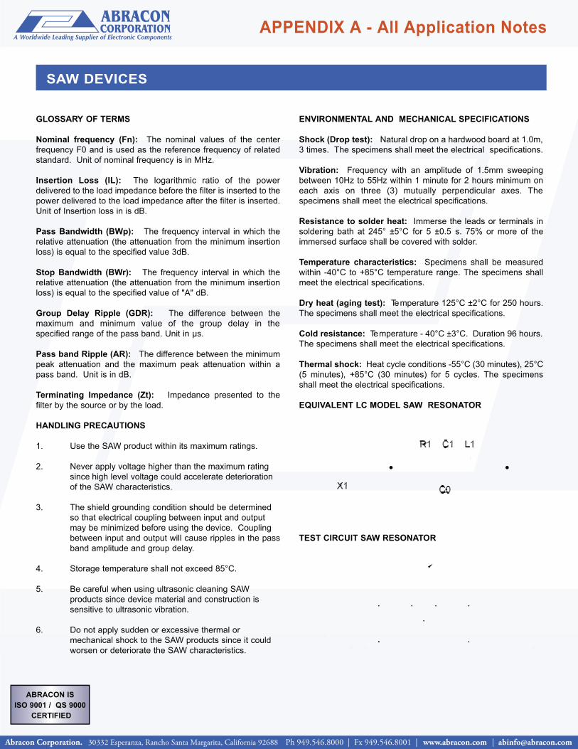
EQUIVALENT LC MODEL SAW RESONATOR
TEST CIRCUIT SAW RESONATOR
APPENDIX A - All Application Notes
SAW DEVICES
Abracon Corporation. 30332 Esperanza, Rancho Santa Margarita, California 92688 Ph 949.546.8000 | Fx 949.546.8001 | www.abracon.com | [email protected]
ABRACON IS ISO 9001 / QS 9000
CERTIFIED
APPLICATION NOTES
SAW DEVICES
Definition of SAW: Surface Acoustic Wave (SAW) is a wave propagating along thesurface of an elastic substrate. Frequency of SAW is:
VF=
Where V is the velocity of SAW ( ~ 3,100m/s)Is the IDT period.
Frequency range of SAW products is 10MHz to 3GHz.
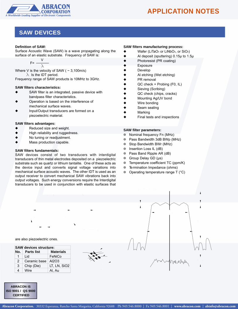
SAW filters characteristics: SAW filter is an integrated, passive device withbandpass filter characteristics.Operation is based on the interference of mechanical surface waves.Input/Output transducers are formed on a piezoelectric material.
SAW filters advantages:Reduced size and weight.High reliability and ruggedness.No tuning or readjustment.Mass production capable.
SAW filters fundamentals:SAW devices consist of two transducers with interdigitaltransducers of thin metal electrodes deposited on a piezoelectricsubstrate such as quartz or lithium tantalite. One of these acts asthe device input and converts signal voltage variations intomechanical surface acoustic waves. The other IDT is used as anoutput receiver to convert mechanical SAW vibrations back intooutput voltages. Such energy conversions require the Interdigitaltransducers to be used in conjunction with elastic surfaces that
are also piezoelectric ones.
SAW devices structure:No. Parts list Materials
1 Lid FeNiCo2 Ceramic base Al2O33 Chip (Die) LT, LN, SiO24 Wire Al, Au
SAW filters manufacturing process:Wafer (LiTaO3 or LiNbO3, or SiO2)Al deposit (sputtering) 0.15μ to 1.5μPhotoresist (PR coating)ExposureDevelopAl etching (Wet etching)PR removalQC check + Probing (F0, IL)Sieving (Scribing)QC check (chips, cracks)Mounting Ag/UV bondWire bondingSeam sealing MarkingFinal tests and inspections
SAW filter parameters: Nominal frequency Fn (MHz)
Pass Bandwidth 3dB BWp (MHz)Stop Bandwidth BWr (MHz)Insertion Loss IL (dB)Pass Band Ripple AR (dB)Group Delay GD (μs)Temperature coefficient TC (ppm/K)Termination Impedance (ohms)Operating temperature range T (°C)
Abracon Corporation. 30332 Esperanza, Rancho Santa Margarita, California 92688 Ph 949.546.8000 | Fx 949.546.8001 | www.abracon.com | [email protected]
ABRACON IS ISO 9001 / QS 9000
CERTIFIED
APPLICATION NOTES
QUARTZ CRYSTAL GLOSSARY OF TERMS
Nominal frequency: The specified center frequency of the crystal. Unitof frequency is Hertz (Hz). Quartz crystals are specified in kHz or MHz.
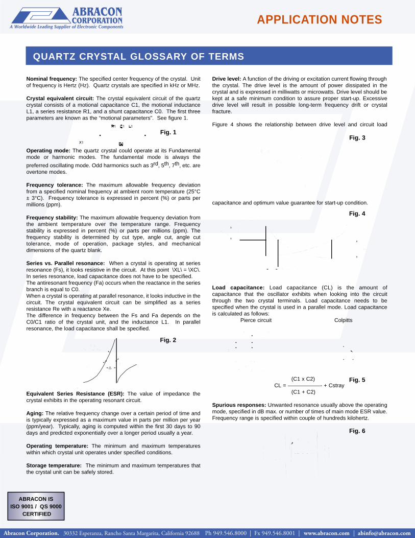
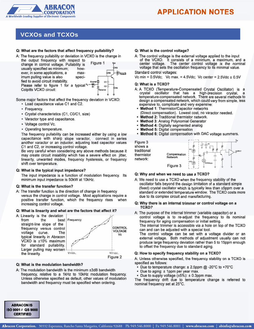
Crystal equivalent circuit: The crystal equivalent circuit of the quartzcrystal consists of a motional capacitance C1, the motional inductanceL1, a series resistance R1, and a shunt capacitance C0. The first threeparameters are known as the “motional parameters”. See figure 1.
Operating mode: The quartz crystal could operate at its Fundamentalmode or harmonic modes. The fundamental mode is always thepreferred oscillating mode. Odd harmonics such as 3rd, 5th, 7th, etc. areovertone modes.
Frequency tolerance: The maximum allowable frequency deviationfrom a specified nominal frequency at ambient room temperature (25°C± 3°C). Frequency tolerance is expressed in percent (%) or parts permillions (ppm).
Frequency stability: The maximum allowable frequency deviation fromthe ambient temperature over the temperature range. Frequencystability is expressed in percent (%) or parts per millions (ppm). Thefrequency stability is determined by cut type, angle cut, angle cuttolerance, mode of operation, package styles, and mechanicaldimensions of the quartz blank.
Series vs. Parallel resonance: When a crystal is operating at seriesresonance (Fs), it looks resistive in the circuit. At this point \XL\ = \XC\.In series resonance, load capacitance does not have to be specified. The antiresonant frequency (Fa) occurs when the reactance in the seriesbranch is equal to C0. When a crystal is operating at parallel resonance, it looks inductive in thecircuit. The crystal equivalent circuit can be simplified as a seriesresistance Re with a reactance Xe.The difference in frequency between the Fs and Fa depends on theC0/C1 ratio of the crystal unit, and the inductance L1. In parallelresonance, the load capacitance shall be specified.
Equivalent Series Resistance (ESR): The value of impedance thecrystal exhibits in the operating resonant circuit.
Aging: The relative frequency change over a certain period of time andis typically expressed as a maximum value in parts per million per year(ppm/year). Typically, aging is computed within the first 30 days to 90days and predicted exponentially over a longer period usually a year.
Operating temperature: The minimum and maximum temperatureswithin which crystal unit operates under specified conditions.
Storage temperature: The minimum and maximum temperatures thatthe crystal unit can be safely stored.
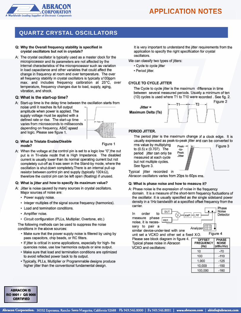
Drive level: A function of the driving or excitation current flowing throughthe crystal. The drive level is the amount of power dissipated in thecrystal and is expressed in milliwatts or microwatts. Drive level should bekept at a safe minimum condition to assure proper start-up. Excessivedrive level will result in possible long-term frequency drift or crystalfracture.
Figure 4 shows the relationship between drive level and circuit load
capacitance and optimum value guarantee for start-up condition.
Load capacitance: Load capacitance (CL) is the amount ofcapacitance that the oscillator exhibits when looking into the circuitthrough the two crystal terminals. Load capacitance needs to bespecified when the crystal is used in a parallel mode. Load capacitanceis calculated as follows:
Pierce circuit Colpitts
(C1 x C2)CL = ——————- + Cstray
(C1 + C2)
Spurious responses: Unwanted resonance usually above the operatingmode, specified in dB max. or number of times of main mode ESR value.Frequency range is specified within couple of hundreds kilohertz.
Fig. 1
Fig. 2
Fig. 3
Fig. 4
Fig. 6
Fig. 5
Abracon Corporation. 30332 Esperanza, Rancho Santa Margarita, California 92688 Ph 949.546.8000 | Fx 949.546.8001 | www.abracon.com | [email protected]
ABRACON IS ISO 9001 / QS 9000
CERTIFIED
APPLICATION NOTES
QUARTZ CRYSTAL GLOSSARY OF TERMS
Crystal cuts: A blank wafer is obtained by cutting the quartz barat specific angles to the various axes. The choice of axis andangle cut determines the physical and electrical parameters ofthe resonator. Figure 7 shows combinations of X, Y, and Zrotational cuts which are labeled in industry as AT, BT, CT, DTcut, etc. The most two common cuts in Abracon crystals are ATand BT-cuts. There are differences in temperature coefficients ofthe two cuts.
Vibration modes: The crystal vibrates and produces a steadysignal when it is excited with a voltage. The mode of vibrationdepends on crystal cuts such as thickness shear for AT and BTcuts, length-width flexure for tuning fork, Face shear for CT, DTcuts, etc. Figure 8 shows a thickness-shear mode.
Shunt capacitance C0: The static capacitance between theelectrodes (Ce) together with holder capacitance (Ch).
Co = Ce + ChCh varies between 0.6pF to 0.8pF depending on mountingmethod.Motional capacitance C1: The capacitance of the nominal armof the equivalent circuit. C1 results from the elasticity of thequartz blank.
C1 (pF) = 0.22 x A (m2) x F (Hz) / 1670Where A = area of electrode in m2
Quality factor Q: The factor that represents the sharpness of theresonant curve. Quartz crystal has a very high Q compared toother resonators typically in 10,000 to 100,000s.
2 * ππ ∗∗ Fs * L1 1Q = =
R1 2 * ππ ∗∗ Fs * C1 * R1Pullability: When a crystal is operating at parallel resonance, itlooks inductive in the circuit. As the reactance changes, thefrequency changes correspondingly, thus change the pullabilityof the crystal. The difference in frequency between the Fs andFa depends on the C0/C1 ratio of the crystal unit and the loadcapacitance CL.Delta F from series resonant to parallel resonant in ppm:
FL – Fs ΔΔF C1= =
Fs Fs 2 (C0 + CL)Pullability can be expressed in terms of load sensitivity (TS) inppm/pF.
106 * C1TS (ppm/pF) =
2 (C0 + CL)2
Negative resistance (-R): Negative resistance is used to evalu-ate circuit oscillation allowance. Lack of negative resistancecould lead to initial circuit start-up and and unstable oscillationat steady state.Procedure:1. Connect the external resistance Ri in series with the crystal.2. Adjust Ri value until oscillation stops.3. Record Ri value.4. Negative resistance –R = Ri + R15. Recommended - R value to be at least 5 to 10 times greater
than Re.
See figure 9.Frequency vs. temperature characteristics: Figure 10 showsthe frequency – temperature characteristics for a thickness-shear AT cut crystal. The AT-cut curve has an S-shapesymmetrical to room temperature.Quartz crystals manufacturing process: Quartz crystals are
manufactured in a clean environment to assure high-precision.Highlights of the major steps in manufacturing process of the AT-Cut crystal are described below:
As grown quartz bars – Lumbering – Cutting – Measurement ofangle – Precision lapping – Beveling – Etching and Cleaning –Base coating – Mounting – Fine frequency adjusting – Annealing– Sealing – Aging – Final tests and Inspections.
Crystal mounting methods: Quartz blank unit is mounted onholder mounts with conductive epoxy or solder (tuning fork).Precise amount of silver epoxy is applied with automounter
Fig. 7
Fig. 9
Fig. 10
Fig. 11
Fig. 8
Abracon Corporation. 30332 Esperanza, Rancho Santa Margarita, California 92688 Ph 949.546.8000 | Fx 949.546.8001 | www.abracon.com | [email protected]
ABRACON IS ISO 9001 / QS 9000
CERTIFIED
APPLICATION NOTES
QUARTZ CRYSTALS
The following considerations must be well studied in order to select the right crystal for your applications:1) ASIC CHARACTERISTICS:
• Negative resistance.• Small-signal gain analysis.• Input and output resistance.• Propagation delay between input and output of inverter.• Gain-phase analysis.• Supply voltage operational margin.• Circuit configuration.• Feedback resistor value (if integrated within the ASIC).• Built-in load capacitance on X1 and X2 ports.• Sensitivity of inverter operation versus stray inductance or
capacitance due to layout or attachment methods.
2) CRYSTAL CHARACTERISTICS:
• Mode of Operation (Fundamental -vs.- Overtone).• Series -vs.- Parallel.• If Parallel: State “Load Capacitance”.• If Overtone: specify design without inductor or conventional
tuning tank LC Circuit.• Maximum Resistance.• Drive Level dependency.• Operating Temperature.• Frequency Accuracy at 25°C.• Frequency Stability over Temperature.• Aging.• Pulling Characteristics.• Spurious Responses.
3) CIRCUIT CONSIDERATIONS:
• Select the best value for Rf (feedback resistor).Recommend Value:
Low kHz Range: between 10 MΩ to 20 MΩMHz Range: between 100kΩ to 1 MΩ
• Select Series Resistance Value (Rd) for impedance matching. Rd selection varies with ASIC negative resistance, output resistance and load impedance. Typical Value for Rd:
0 Ω (Short) to 1 k Ω from 4 MHz to 30 MHz. • Study the Voltage Gain from output to input Vi / Vo = C2 / C1.
It is very common to select equal values of C1 and C2 in thecircuit, but sometimes it is necessary to make the output loadcapacitance (C2) higher to compensate for the signal losses through the crystal and feed back loop.
• Maximum Crystal Resistance Allowed. Low resistance isdesirable for better operational margin and stability. However,crystal resistance varies with frequency, blank size. Low crystalresistance could affect yield and therefore cost.
• Typical Crystal Aging: ± 5 ppm per year maximum. Aging over10 years: ± 10 ppm to ± s15 ppm maximum. Tighter aging (up to±1 ppm per year max.) is available. Tighter aging requires extremely high design, manufacturing and additional post-tests.
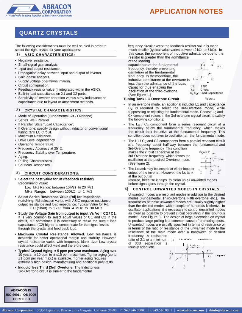
• Inductorless Third (3rd) Overtone: The Inductorless3rd-Overtone circuit is similar to the fundamental
frequency circuit except the feedback resistor value is made much smaller (typical value varies between 2 kΩ to 6 kΩ). Inthis case, the component of inductive admittance due to theresistor is greater than the admittance of the loading capacitance at the fundamental frequency, thereby preventing oscillation at the fundamental frequency. In themeantime, the inductive admittance at the overtone is less than the admittance of the LoadCapacitor thus enabling the oscillation at the third-overtone. (See figure 1.)
Tuning Tank LC Overtone Circuit• In an overtone mode, an additional inductor L1 and capacitance
Cc is required to select the 3rd-Overtone mode, whilesuppressing or rejecting the fundamental mode. Choose Lc and Cc component values in the 3rd-overtone crystal circuit to satisfythe following conditions:
• The Lc / Cc component form a series resonant circuit at afrequency below the fundamental frequency, which makesthe circuit look inductive at the fundamental frequency. Thiscondition does not favor to oscillation at the fundamental mode.
• The L1 / Cc and C2 components form a parallel resonant circuitat a frequency about half-way between the fundamental and3rd-Overtone frequency. This condition makes the circuit capacitive at the 3rd-Overtone frequency, which favors the oscillation at the desired Overtone mode. (See figure 2).
• The Lc tank may be located at either input oroutput of the inverter. However, the Lc tank at the out put is referred, because it helps to clean up all unwanted modes before signal goes through the crystal.
4) CONTROL UNWANTED MODES IN CRYSTALS:Unwanted modes are resonant modes in addition to the desiredmodes (Fundamental, Third-Overtone, Fifth overtone, etc.). Thefrequencies of these unwanted modes are usually slightly higherthan the desired modes within couple of hundreds kilohertz. Inoscillator applications, it is necessary to control unwanted modesas lower as possible to prevent circuit oscillating in the "spuriousmode". See Figure 3. The design of large electrodes on crystalto produce large pulling is a common cause of promoting spurs.Unwanted modes are usually specified in terms of resistance orin terms of the ratio of resistance of the unwanted mode to theresistance of the main mode over a bandwidth of desiredfrequency. A resistanceratio of 2:1 or a minimumof 3dB separation isusually adequate.
U1: ASICY1: CrystalC1 C2: Load Capacitance
Figure 1
Figure 2
Abracon Corporation. 30332 Esperanza, Rancho Santa Margarita, California 92688 Ph 949.546.8000 | Fx 949.546.8001 | www.abracon.com | [email protected]
ABRACON IS ISO 9001 / QS 9000
CERTIFIED
APPLICATION NOTES
QUARTZ CRYSTALS
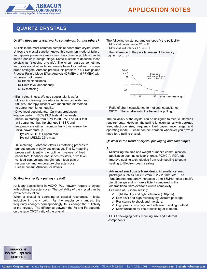
Q: Why does my crystal works sometimes, but not others?
A: This is the most common complaint heard from crystal users.Unless the crystal supplier knows this common mode of failure,and applies preventive measures, this common problem can besolved earlier in design stage. Some customers describe thesecrystals as “sleeping crystals”. The circuit start-up sometimesand does not at other times, unless been touched with a scopeprobe or fingers. Abracon predicts this problem in our Design andProcess Failure Mode Effect Analysis (DFMEA and PFMEA) withtwo main root causes:
a) Blank cleanliness. b) Drive level dependency.c) IC matching.
• Blank cleanliness: We use special blank wafer ultrasonic cleaning procedure in De-ionized water and 99.99% Isopropyl Alcohol with modulated air method to guarantee highest quality.
• Drive level dependency: On most production lots, we perform 100% DLD tests at five levels
minimum starting from 1μW to 500μW. The DLD test will guarantee that the changes in ESR and frequency are within maximum limits thus assure the initial power start-up.
Typical ΔFDLD: ± 5ppm max.Typical ΔRDLD: 25% max.
• IC matching: Abracon offers IC matching process toour customers in early design stage. The IC matching process will identify the optimum values of load capacitors, feedback and series resistors, drive level vs. load cap, voltage margin, open-loop gain at resonance, and temperature characteristics. Please consult Abracon for details.
Q: How to specify a pulling crystal?
A: Many applications in VCXO, PLL network require a crystalwith pulling characteristics. The pullability of the crystal can beexplained as follow:When a crystal is operating at parallel resonance, it looksinductive in the circuit. As the reactance changes, thefrequency changes correspondingly, thus change the pullabilityof the crystal. The difference between the Fs and Fa dependson the ratio C0/C1 ratio of the crystal.
The following crystal parameters specify the pullability:• Motional capacitance C1 in fF.• Motional inductance L1 in mH• The difference of the parallel resonant frequency ΔF = FL2 – FL1
• Ratio of shunt capacitance to motional capacitance C0/C1. The smaller ratio the better the pulling.
The pullability of the crystal can be designed to meet customer’srequirements. However, the pulling function varies with packagesize, electrode size, frequency, load capacitance range, andoperating mode. Please contact Abracon whenever you have aneed for a pulling crystal.
Q: What is the trend of crystal packaging and advantages?
A: • Minimizing the size and weight of mobile communication
application such as cellular phones, PCMCIA, PDA, etc.• Improve sealing technologies from resin sealing to seam
sealing to Electron beam sealing.
• Advanced small quartz blank design in smaller ceramic packages such as 5.0 x 3.2mm, 3.2 x 2.5mm, etc. The fundamental frequency increases up to 66MHz helps simplifycircuit design and is more efficient compared to the old traditional third-overtone circuit complexity.
• Features of E-Beam sealing: Tight stability and tight tolerance (±10ppm). Low ESR and high reliability by vacuum package. Resistance to shock and moisture. High productivity captured with seam sealing method. Miniaturization by fine processing of E-Beam.
• LTCC packaging helps reducing size and external components.
Abracon Corporation. 30332 Esperanza, Rancho Santa Margarita, California 92688 Ph 949.546.8000 | Fx 949.546.8001 | www.abracon.com | [email protected]
ABRACON IS ISO 9001 / QS 9000
CERTIFIED
APPLICATION NOTES
ULTRA LOW NOISE SPREAD-SPECTRUM CRYSTAL OSCILLATORS
EMI Protection and Spread-SpectrumTechnology:
The FCC and the European Community (under CEMark EMC Directive) require electronic devices to comply with appropriate radiation emission standards.Other international communities such as Asia andAustralia are also following the same rules. Practicallyevery electric device and equipment generateunintended electromagnetic radiation, which will getworse as technology advances, especially with evenfaster electrical signals required in PC, digital devicesand equipment.
With the recent advance in semiconductor and computing technology, (faster clock speeds, lower voltage/power, etc.), coupled with the explosion of thewireless technologies, it is easy to understand whyEMC is becoming one of the most important standardrequirements in the new-technology world.
In the past, shielding and filtering were the most prevalent method used to control EMI. This method ofshielding and filtering can get very expensive. As frequency increases, the effects of transmission lineand ground impedance will amplify the radiation, and atthe same time wavelength decreases, making shieldingand filtering less effective.
The present trend is to control EMI at the source, thesingle clock oscillator using spread-spectrumtechnology.
THEORY:
Spread-spectrum is, more or less, frequency modulating the clock signal with a unique waveform.In the frequency domain, this is equivalent to reducing the peak by distributing the energy of eachfundamental and harmonic over a wide range. Thespread-spectrum method must be controlled andslow compared to the clock rate to guarantee thatthe change in the clock rate is transparent to thesystem. Essentially, spread-spectrum is a modulation method where the modulation is measured as a percentage.
For example, a 0.5 percent modulation means that a100MHz clock is modulated between 99.5MHz and100.5MHz. This is called a center 0.5 percent modulation, since the 100MHz fundamental frequency remains the center frequency. The designer must keep in mind that both cycle-to-cycleand pea-to-peak jitter must remain within the system’s specifications.
Another important factor is the modulation frequency,which is usually in the kilohertz range. This is basically a measure of the rate at which the frequency is swept between 99.5 and 100.5. The linear sweep is predictable and most prevalent.
Overall, the spread spectrum method has allowedsystem performance to increase without compromising EMI. Using Abracon spread-spectrumclock oscillators will not only reduce packaging,shielding, and design-cycle costs, but also expeditetime-to-market of products which therwise may failregulatory EMI limits and standards. Abracon ultralow noise series oscillators provide an economicalsolution to expensive EMI problems.
Abracon Corporation. 30332 Esperanza, Rancho Santa Margarita, California 92688 Ph 949.546.8000 | Fx 949.546.8001 | www.abracon.com | [email protected]
ABRACON IS ISO 9001 / QS 9000
CERTIFIED
APPLICATION NOTES
LOW EMI CRYSTAL CLOCK OSCILLATORS
Spread Spectrum Technology used to reduce EMI has been integrated into industry standard 8 and 14 pin DIPpackages and surface mount versions as small as 5 X 7 mm. These products are perfect drop-in replacement clockoscillators where EMI reduction of up to 20 dB is needed.
Typical system designs start out with some fundamental clock source, such as a crystal, ceramic or can oscillator,at some frequency, lets say 48 MHz, which drives a processor, memory, serial/USB interfaces and some front panelcontrols. The 48 MHz clock is changed into other timing components such as clock multipliers found in PLL basedprocessors, memory controllers, and interface controllers. The original 48 MHz clock quickly becomes 96 MHz or24 MHz to drive a serial interface. These fundamental and harmonic frequencies can make it very difficult for com-pliance engineers to achieve certification.During the design phase, if the proper package and frequency is chosen for the clock source, the flexibility in futuremodifications is increased. Even after the design phase is done, there will always be hot spots that will require someform of filtering or shielding. If all that is needed is to slow down the rise time of one or two specific nets, but thisis not usually the case. If, however, the EMC engineer sees that the agency limits have been exceeded by 10 dBin several higher frequency harmonics, production must wait until compliance is achieved. When this happens,there are 3 possible ways to solve the problem, re-design in an attempt reduce EMI, filter and shield every net thatis offending compliance or change the bill of material to call out a Low EMI Clock Oscillator.
SSC takes advantage of the fact that a frequency-modulated carrier will have lower peak energy than a non-mod-ulated carrier. By frequency modulating the carrier, the energy is spread out over a wider range of frequencies,thereby reducing the peak energy contained in any one frequency. Comparing a modulated clock to a non-modu-lated clock on a spectrum analyzer, it can be seen that the peaks of the modulated clock and harmonic frequen-cies are lower in relative strength. The difference in relative strength of the energy of the clock is measured in dB.Sweeping the frequency of the fundamental clock back and forth at some rate will cause a reduction in peak ener-gy. The wider the spread the greater the peak energy reduction. To determine how much spread you need for agiven application use the simple formula below to calculate the necessary dB reduction. This formula assumes anideal clock with a 50% duty cycle and only predicts the EMI reduction of odd harmonics. Calculation for dB reduction:
dB = 6.5 + 9(Log10(F)) + 9(Log10(BW))
Where; F = Frequency in MHz and BW = total % spread (2.5% = .025)
Using a 96 and 480 MHz clock with a 2.5% spread, the theoretical dB reduction would be;dB @ 96 MHz (Fund) = 6.5 + 17.84 – 14.4 = 9.92dB @ 480 MHz (5th) = 6.5 + 24.13 – 14.4 = 16.21
Regulatory agencies control the maximum amount of radiated RF energy. Unwanted RF energy is considered EMI,which causes interference in local receiving equipment such as television, radio, cell phones and pagers.
Agencies, such as the Federal Communications Commission, regulate the amount of radiated energy in terms ofvoltage, distance and frequency. The FCC has two classes of radiation levels, stated as Class A and Class B.Class A devices are digital devices intended for use in commercial, industrial or businesses and not intended foruse by the general public or in the home. Class B digital devices are intended to be used in the home but couldalso be used elsewhere. In gereral, Class B levels are more difficult to meet than Class A.
Abracon Corporation. 30332 Esperanza, Rancho Santa Margarita, California 92688 Ph 949.546.8000 | Fx 949.546.8001 | www.abracon.com | [email protected]
ABRACON IS ISO 9001 / QS 9000
CERTIFIED
APPLICATION NOTES
LOW EMI CRYSTAL CLOCK OSCILLATORS
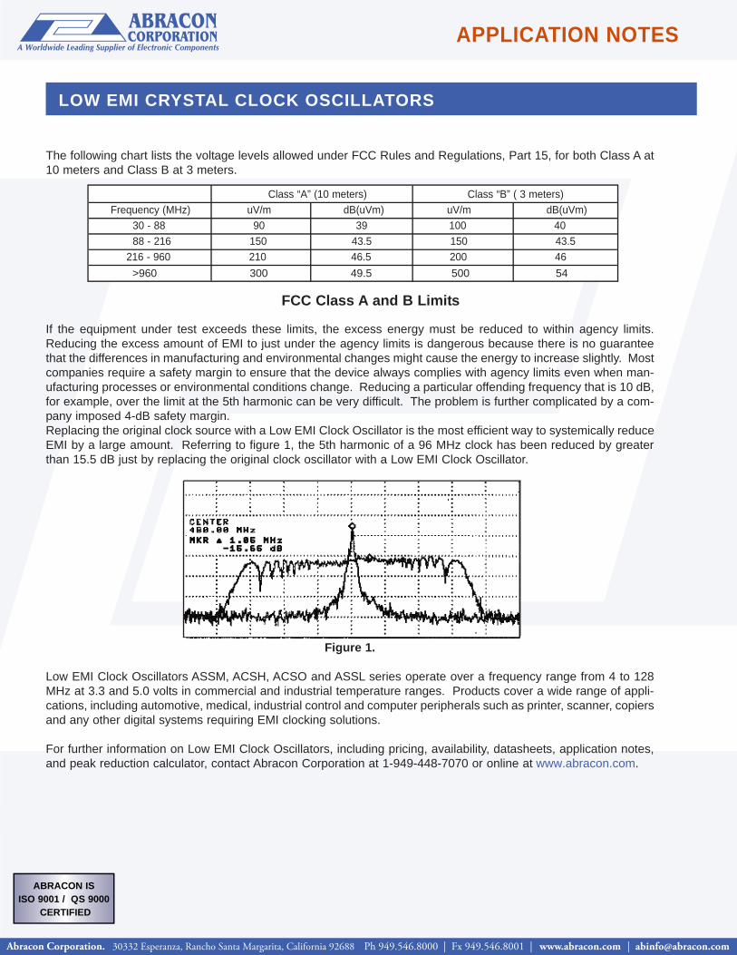
The following chart lists the voltage levels allowed under FCC Rules and Regulations, Part 15, for both Class A at10 meters and Class B at 3 meters.
FCC Class A and B Limits
If the equipment under test exceeds these limits, the excess energy must be reduced to within agency limits.Reducing the excess amount of EMI to just under the agency limits is dangerous because there is no guaranteethat the differences in manufacturing and environmental changes might cause the energy to increase slightly. Mostcompanies require a safety margin to ensure that the device always complies with agency limits even when man-ufacturing processes or environmental conditions change. Reducing a particular offending frequency that is 10 dB,for example, over the limit at the 5th harmonic can be very difficult. The problem is further complicated by a com-pany imposed 4-dB safety margin. Replacing the original clock source with a Low EMI Clock Oscillator is the most efficient way to systemically reduceEMI by a large amount. Referring to figure 1, the 5th harmonic of a 96 MHz clock has been reduced by greaterthan 15.5 dB just by replacing the original clock oscillator with a Low EMI Clock Oscillator.
Figure 1.
Low EMI Clock Oscillators ASSM, ACSH, ACSO and ASSL series operate over a frequency range from 4 to 128MHz at 3.3 and 5.0 volts in commercial and industrial temperature ranges. Products cover a wide range of appli-cations, including automotive, medical, industrial control and computer peripherals such as printer, scanner, copiersand any other digital systems requiring EMI clocking solutions.
For further information on Low EMI Clock Oscillators, including pricing, availability, datasheets, application notes,and peak reduction calculator, contact Abracon Corporation at 1-949-448-7070 or online at www.abracon.com.
Class “A” (10 meters) Class “B” ( 3 meters)Frequency (MHz) uV/m dB(uVm) uV/m dB(uVm)
30 - 88 90 39 100 4088 - 216 150 43.5 150 43.5
216 - 960 210 46.5 200 46>960 300 49.5 500 54
FCC Class A and B Limits
Abracon Corporation. 30332 Esperanza, Rancho Santa Margarita, California 92688 Ph 949.546.8000 | Fx 949.546.8001 | www.abracon.com | [email protected]
ABRACON IS ISO 9001 / QS 9000
CERTIFIED
APPLICATION NOTES
LOW EMI CRYSTAL CLOCK OSCILLATORS
MODULATION FREQUENCY
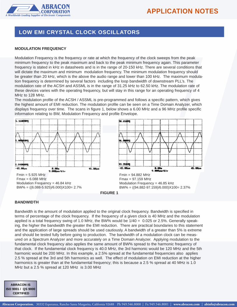
Modulation Frequency is the frequency or rate at which the frequency of the clock sweeps from the peakminimum frequency to the peak maximum and back to the peak minimum frequency again. This parameterfrequency is stated in kHz in datasheets and is in the range of 20-150 kHz. There are several conditions thatwill dictate the maximum and minimum modulation frequency. The minimum modulation frequency shouldbe greater than 20 kHz, which is the above the audio range and lower than 100 kHz. The maximum modula-tion frequency is determined by several factors including the loop bandwidth of downstream PLL’s. Themodulation rate of the ACSH and ASSML is in the range of 31.25 kHz to 62.50 kHz. The modulation rate ofthese devices varies with the operating frequency, but will stay in this range for an operating frequency of 4MHz to 128 MHz.The modulation profile of the ACSH / ASSML is pre-programmed and follows a specific pattern, which givesthe highest amount of EMI reduction. The modulation profile can be seen on a Time Domain Analyzer, whichdisplays frequency over time. The scans in figure 1, below shows a 6.00 MHz and a 96 MHz profile specificinformation relating to BW, Modulation Frequency and profile Envelope.
FIGURE 1
BANDWIDTH
Bandwidth is the amount of modulation applied to the original clock frequency. Bandwidth is specified interms of percentage of the clock frequency. If the frequency of a given clock is 40 MHz and the modulationapplied is a total frequency swing of 1.0 MHz, the BW% would be 1/40 = 0.025 or 2.5%. Generally speak-ing, the higher the bandwidth the greater the EMI reduction. There are practical boundaries to this statementand the application of large spreads should be used cautiously. A bandwidth of a greater than 5% is extremeand should be tested fully before going to production. The bandwidth of a modulation clock can be meas-ured on a Spectrum Analyzer and more accurately on a Time Domain Analyzer. Applying modulation to thefundamental clock frequency also applies the same amount of BW% spread to the harmonic frequency ofthat clock. If the fundamental clock frequency is 40.0 MHz, the 3rd harmonic would be 120 MHz and the 5thharmonic would be 200 MHz. In this example, a 2.5% spread at the fundamental frequencies also applies2.5 % spread at the 3rd and 5th harmonics as well. The effect of modulation on EMI reduction at the higherharmonics is greater than at the fundamental frequency; this is because a 2.5 % spread at 40 MHz is 1.0MHz but a 2.5 % spread at 120 MHz is 3.00 MHz
Fmin = 5.925 MHzFmax = 6.088 MHzModulation Frequency = 46.84 kHzBW% = ((6.088-5.925)/6.000)X100= 2.7%
Fmin = 94.882 MHzFmax = 97.159 MHzModulation Frequency = 46.85 kHzBW% = ((94.882-97.159)/6.000)X100= 2.37%
Abracon Corporation. 30332 Esperanza, Rancho Santa Margarita, California 92688 Ph 949.546.8000 | Fx 949.546.8001 | www.abracon.com | [email protected]
ABRACON IS ISO 9001 / QS 9000
CERTIFIED
APPLICATION NOTES
CERAMIC RESONATORS
Why Ceramic Resonators? Ceramic resonators stand betweenquartz crystals and LC/RC oscillators in regard to accuracy.They offer low cost and high reliability timing devices withimproved start-up time to quartz crystals.
Package styles: Abracon offers a wide variety of packagestyles for ceramic resonators. They come with two or threeterminals leaded type or surface-mount type. We also offer thewashable industrial grade ceramic resonators with gold flash ter-minals on the surface-mount types (AWSCR, AWSZT).
Properties: The oscillation of ceramic resonators isdependent upon mechanical resonance associated with theirpiezoelectric crystal structure. These materials (usually BariumTitanate or Lead-Zirconium Titanate) have large dipolemovement, which causes the distortion or growth of the wafer byan applied electric field.
Oscillation mode: The ceramic resonator oscillates inthickness-shear vibration mode for Fundamental frequencies(typical less or equal than 8MHz) and thickness-longitudinalvibration mode for third-overtone mode (above 8MHz to 50MHz).
Frequency range: The available frequency range varies from182kHz to 50MHz.
Frequency tolerance at 25°C: The maximum allowablefrequency deviation from the nominal frequency at roomtemperature. Frequency tolerance is expressed in percent.Typical frequency tolerance is ± 0.5% max. Frequencytolerance can be controlled tighter on built-in capacitance type.
Frequency stability: The maximum allowable deviationcompared to the measured frequency at 25°C over thetemperature window, i.e. –20°C to +80°C or –40°C to +125°C.Standard frequency stability is ± 0.3%.
Resonant Impedance: The net impedance of the ceramicresonator at resonant frequency. Ceramic resonators havesuperior resonant impedance than quartz crystal, which offermuch better start-up time.
Aging: The relative frequency change over 10 years period. Theaging is ± 0.3% max. over 10 years.
Load capacitance CL: Since ceramic resonators have verylarge parallel resonance area and frequency is very sensitive toload capacitance, exact value of load capacitance must bespecified. This process is usually been done through ICmatching and characterization. Please contact Abracon fordetails.
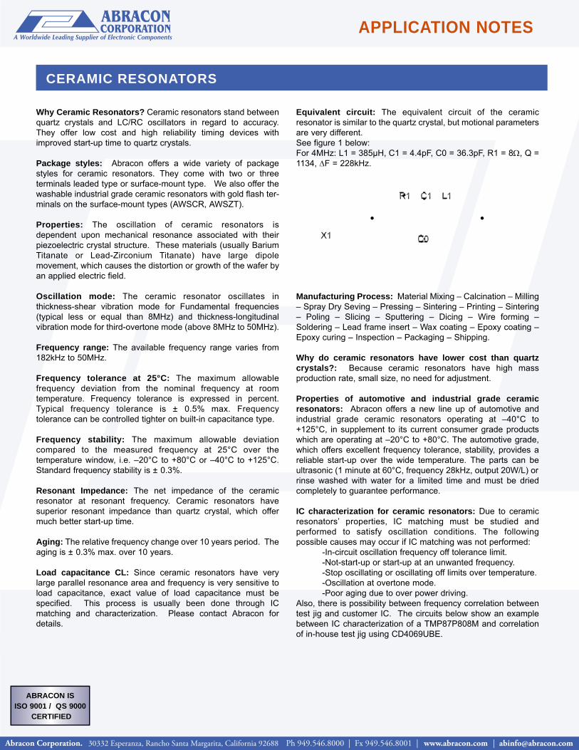
Equivalent circuit: The equivalent circuit of the ceramicresonator is similar to the quartz crystal, but motional parametersare very different.See figure 1 below:For 4MHz: L1 = 385μH, C1 = 4.4pF, C0 = 36.3pF, R1 = 8Ω, Q =1134, ΔF = 228kHz.
Manufacturing Process: Material Mixing – Calcination – Milling– Spray Dry Seving – Pressing – Sintering – Printing – Sintering– Poling – Slicing – Sputtering – Dicing – Wire forming –Soldering – Lead frame insert – Wax coating – Epoxy coating –Epoxy curing – Inspection – Packaging – Shipping.
Why do ceramic resonators have lower cost than quartzcrystals?: Because ceramic resonators have high massproduction rate, small size, no need for adjustment.
Properties of automotive and industrial grade ceramicresonators: Abracon offers a new line up of automotive andindustrial grade ceramic resonators operating at –40°C to+125°C, in supplement to its current consumer grade productswhich are operating at –20°C to +80°C. The automotive grade,which offers excellent frequency tolerance, stability, provides areliable start-up over the wide temperature. The parts can beultrasonic (1 minute at 60°C, frequency 28kHz, output 20W/L) orrinse washed with water for a limited time and must be driedcompletely to guarantee performance.
IC characterization for ceramic resonators: Due to ceramicresonators’ properties, IC matching must be studied andperformed to satisfy oscillation conditions. The followingpossible causes may occur if IC matching was not performed:
-In-circuit oscillation frequency off tolerance limit.-Not-start-up or start-up at an unwanted frequency.-Stop oscillating or oscillating off limits over temperature.-Oscillation at overtone mode.-Poor aging due to over power driving.
Also, there is possibility between frequency correlation betweentest jig and customer IC. The circuits below show an examplebetween IC characterization of a TMP87P808M and correlationof in-house test jig using CD4069UBE.
Abracon Corporation. 30332 Esperanza, Rancho Santa Margarita, California 92688 Ph 949.546.8000 | Fx 949.546.8001 | www.abracon.com | [email protected]
ABRACON IS ISO 9001 / QS 9000
CERTIFIED
APPLICATION NOTES
CERAMIC RESONATORS
IC characterization steps:Frequency correlation between customer’s IC and standard ICtested.Temperature characteristics of oscillating frequency.Temperature characteristics of oscillating voltage.Rise time vs. Vdd characteristics.Oscillating frequency vs. Vdd characteristics.Oscillating voltage vs. Vdd characteristics.Oscillating frequency vs. C1 values (C2 constant)Oscillating frequency vs. C2 values (C1 constant)Oscillating voltage vs. C1 values (C2 constant)Oscillating voltage vs. C2 values (C1 constant)Oscillating frequency vs. CL value (C1 = C2)Oscillating voltage vs. CL value (C1 = C2)Rise time vs. CL characteristics (C1 = C2)Starting voltage vs. CL characteristics (C1 = C2)
Polarization on ceramic resonators: Both quartz crystals andceramic resonators do not have polarity since leads can bemounted interchangeably. However, since ceramic resonator hasmuch wider trim sensitivity vs. load capacitors value ± 20%, werecommend mounting in the same way as we do thecharacterization.
IC characterization request: Abracon will offer our customer, inmost cases, IC characterization at no cost. It is very important tohave this process done in early stage of design and boardevaluation. However, please allow us extra time to complete andsubmit the report. We need the following information to sendalong when submitting a request:
Application. Please be specific either automotive or consumergrade applications. Package style (leaded or surface-mount).Electrical parameters.Estimate annual usage.Pilot run and production date.IC part number and manufacturerApplied voltage and tolerance, e.g. 12Vdc ± 10%Operating temperature.2 to 5 bulk IC samples or the actual PCB with components
mounted in oscillator section. The PCB is preferred so that parasiticeffects on the board can be taken into account.A top view pin assignment for the package of the IC samples.Attached schematic shown values of components values such asRd, Rf, C1, C2, etc.Specify date needed.Name and E-mail contact.
As soon as we received the complete information and materials asspecified, we will submit the report and recommendations within 4to 6 weeks.
LAYOUT HINTS:When you design circuit on a PCB, please take the followingconsiderations:
Please design the trace length as short as possible.Try to avoid thin line on resonator traces (< 0.010”). Design aswide as possible.If noise occurs, please insert EMI filter with serial mode betweenXOUT pin and resonator or between capacitor and GND.
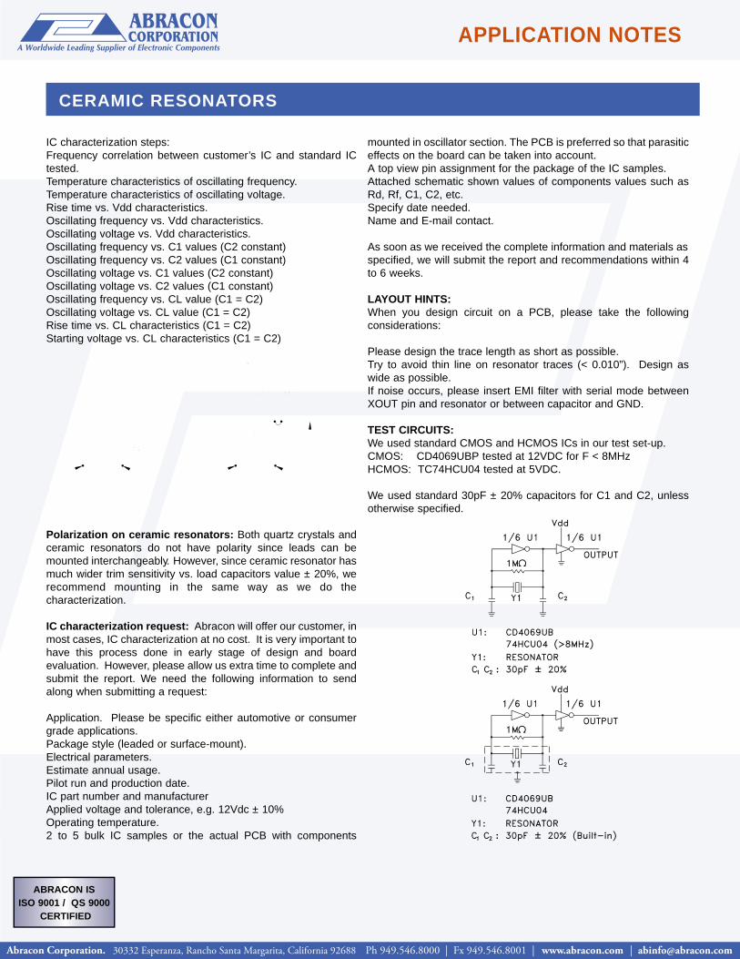
TEST CIRCUITS:We used standard CMOS and HCMOS ICs in our test set-up. CMOS: CD4069UBP tested at 12VDC for F < 8MHzHCMOS: TC74HCU04 tested at 5VDC.
We used standard 30pF ± 20% capacitors for C1 and C2, unlessotherwise specified.

Abracon Corporation. 30332 Esperanza, Rancho Santa Margarita, California 92688 Ph 949.546.8000 | Fx 949.546.8001 | www.abracon.com | [email protected]
ABRACON IS ISO 9001 / QS 9000
CERTIFIED
APPLICATION NOTES
QUARTZ CRYSTAL OSCILLATORS GLOSSARY OF TERMS
Nominal frequency: The center or nominal output frequency of acrystal oscillator.Package: Crystal oscillators are packaged in various styles from leadthrough holes to surface-mount types. Various sizes and functions aresuitable for different applications.Frequency tolerance: The deviation from the nominal frequency interms of parts per millions (ppm) at room temperature. (25° ± 5°C)Frequency range: The frequency band that the oscillator type ormodel can be offered.Frequency stability: The maximum allowable frequency deviationcompared to the measured frequency at 25 °C over the temperaturewindow, i.e., 0° C to +70° C. Typical stability is ± 0.01% ( ±100 ppm).Operating temperature: Temperature range within which outputfrequency and other electrical, environmental characteristics meet thespecifications.Aging: The relative frequency change over a certain period of time.This rate of change of frequency is normally exponential in character.Typically, aging is ± 5ppm over 1 year maximum.Storage Temperature: The temperature range where the unit issafely stored without damaging or changing the performance of theunit.Frequency vs. Power Supply Variation: Maximum frequency changeallowed when the power supply voltage is changed within its specifiedlimits (typical ± 10% in VCC or ± 5% change).Supply Voltage (Vdd max): The maximum voltage which can safelybe applied to the Vcc terminal with respect to ground. Maximumsupply voltage for TTL is 5.5V and for HCMOS is 7V.Input Voltage (VIN): The maximum voltage that can be safely appliedto any input terminal of the oscillator.Output HIGH voltage (VOH): The minimum voltage at an output ofthe oscillator under proper loading.Output LOW voltage (V0H): The maximum voltage at an output ofthe oscillator under proper loading.Input HIGH voltage (VIH): The minimum voltage to guaranteethreshold trigger at the input of the oscillator.Input LOW voltage (VIL): The maximum voltage to guarantee thethreshold trigger at the input of the oscillator.Supply Current (lcc): The current flowing into Vcc terminal withrespect to ground. Typical supply current is measured without load.Symmetry or Duty Cycle: The symmetry of the output waveform atthe specified level (at 1.4V for TTL, at 1/2 Vcc for HCMOS, or 1/2waveform peak level for ECL).See Fig. 1SYM = tH x 100 (%)T
Fan Out: The measure of driving ability of an oscillator, expressedas the number of inputs that can be driven by a single output. It canbe represented by an equivalent load capacitance (CL) or a TTL loadcircuit consisting of diodes, load resistor, and a capacitor.
Rise Time (Tr ): Waveform rise time from Low to High transition,measured at the specified level
10% to 90% for HCMOS, 20% to 80% for ECL0.4V to 2.4V for TTL.
Fall Time (Tf ): The waveform fall time from High to Low transition,measured at the specified level
90% to 10% for HCMOS, 80% to % for ECL2.4V to 0.4V for TTL.
Jitter: The modulation in phase or frequency of oscillator output.HCMOS / TTL Compatible: The oscillator is designed with ACMOSlogic with driving capability of TTL and HCMOS loads whilemaintaining minimum logic HIGH of the HCMOS.Tristate Enable: When the input is left OPEN or tied to logic “1”, thenormal oscillation occurs. When the input is Grounded (tied to logic“0”), the output is in high impedance state. The input has an internalpull-up resistor thus allowing the input to be left open.Output Logic: The output of an oscillator is designed to meetvarious specified logic states, such as TTL, HCMOS, ECL, Sine,Clipped-Sine (DC cut).Harmonic Distortion: The non-linear distortion due to unwantedharmonic spectrum component related with target signal frequency.Each harmonic component is the ratio of electric power againstdesired signal output electric power and is expressed in terms of dBc,i.e. -20dBc. Harmonic distortion specification is important especiallyin sine output when a clean and less distorted signal is required.Phase Noise: The measure of the short-term frequency fluctuations of the oscillator. It is usually specified as the single sideband (SSB) power density in a 1Hz bandwidth at a specified offsetfrequency from the carrier. It is measured in dBc/Hz.
Stand By: A function that temporary turns off the oscillator and otherdividers to save power. Logic “0” will enable stand by mode. Thedisable current at stand by mode varies from a few micro-amperes totens of micro-amperes (5μA typical). Because oscillation is halted,there is a maximum of 10 ms (same amount of start-up time) beforeoutput stabilizes.
Figure 1.

Abracon Corporation. 30332 Esperanza, Rancho Santa Margarita, California 92688 Ph 949.546.8000 | Fx 949.546.8001 | www.abracon.com | [email protected]
ABRACON IS ISO 9001 / QS 9000
CERTIFIED
APPLICATION NOTES
QUARTZ CRYSTAL OSCILLATORS
Q: Introduction to Abracon Programmable Oscillators:A: Abracon offers quick-turn programmable oscillators in four differentpackage styles; the ceramic package 7.0 x 5.0 x 1.6 mm, plasticmolded package similar to Epson SG-8002, and the 14 pin and 8 pindip packages. The single PLL architecture with EPROMprogrammable generates a custom frequency derived from an internalcrystal between 10MHz to 25MHz. The main advantages of theprogrammable oscillators are:
Easy customization and fast turnaround.Wide frequency ranges 1MHz to 133MHz.Programming accuracy > 6 digits.Output control Synchronous or Asynchronous.Output levels CMOS or TTL.Fast rise and fall times.Fast programming time < 5 seconds per unit.Low skew, low jitter, high accuracy outputs.Enables design flexibility and easy of use.Powerdown and output enable options available.Configurable 5V or 3.3VDC operation in seconds.Reprogrammable for quick design changes (applied to blank only).Extended temperature -40°C to +85°C with good frequency vs. temperature characteristics.
Q: What is PLL technology?A: A PLL allows a frequency to be generated from any otherfrequency, where:
REF. CLK * P/QCLK OUT =
Post-Divider
Q: What is jitter?A: Jitter is the uncertainty or short-term variations of a digital waveformtiming from their ideal positions in time.The waveform transition could be too early or too late compared to theideal waveform timing.
Q: How to measure jitter?A: We use LeCroy digitizing oscilloscope with jitter timing software forjitter measurement and analysis. The scope must have thebandwidth at least five times the frequency of the waveform since thewaveform jitter is measured as each rising cycle crosses thethreshold voltage. The larger number of continuous cycles the moreaccurate is the jitter distribution. Jitter is measured in cycle-to-cycle
(or absolute jitter) or one sigma jitter (rms.) using the histogramanalysis. Unit of jitter is ps.
Q: Can phase noise be improved in designs?A: Yes. Crystal oscillators can be designed to minimize their phasenoise characteristics. Special applications such as wireless requirebest phase noise both at far-end and close-end. Crystal parametersand mounting methods directly affect close-end phase noise 300Hzoffset from carrier. The oscillator front-end and output buffer
Abracon Corporation. 30332 Esperanza, Rancho Santa Margarita, California 92688 Ph 949.546.8000 | Fx 949.546.8001 | www.abracon.com | [email protected]
ABRACON IS ISO 9001 / QS 9000
CERTIFIED
APPLICATION NOTES
QUARTZ CRYSTAL OSCILLATORS
h 4 46 | 4 46 | b | b f b
APPLICATION A NOTES
QUARTZ CRYSTAL OSCILLATORS

Abracon Corporation. 30332 Esperanza, Rancho Santa Margarita, California 92688 Ph 949.546.8000 | Fx 949.546.8001 | www.abracon.com | [email protected]
ABRACON IS ISO 9001 / QS 9000
CERTIFIED
APPLICATION NOTES
QUARTZ CRYSTAL OSCILLATORS
APPLICATION A NOTES
QUARTZ CRYSTAL OSCILLATORS
Abracon Corporation. 30332 Esperanza, Rancho Santa Margarita, California 92688 Ph 949.546.8000 | Fx 949.546.8001 | www.abracon.com | [email protected]
ABRACON IS ISO 9001 / QS 9000
CERTIFIED
APPLICATION NOTES
VCXOs and TCXOs
APPLICATION A NOTES
VCXOs and TCXOs
racon Corporation. 30332 Esperanza, Rancho Santa Margarita, California 92688 Ph 949.546.8000 | Fx 949.546.8001 | wwwww .abracon.comww | [email protected]
Abracon Corporation. 30332 Esperanza, Rancho Santa Margarita, California 92688 Ph 949.546.8000 | Fx 949.546.8001 | www.abracon.com | [email protected]
ABRACON IS ISO 9001 / QS 9000
CERTIFIED
APPLICATION NOTES
MONOLITHIC QUARTZ CRYSTAL FILTERS
Holder: A case housing a thin piece of quartz crystal withvacuum-evaporated metal electrodes and terminals for connections.
Nominal Frequency: Normally this refers to the nominal value ofthe center frequency given in the specifications, to which otherfrequencies may be referred. Nominal frequency usually indicatesthe Center Frequency (Fo) and Carrier Frequency (Fc).
Pass Bandwidth: The pass bandwidth in which the attenuation isequal to or less than a specified value insertion loss.
Stop Bandwidth: The stop bandwidth in which the attenuationsare equal to or greater than specified values in the stop bandattenuation.
Ripple: The ripple (in pass band) is the difference between themaximum and minimum attenuation within a passband.
Insertion Loss: The logarithmic ratio of the power delivered to theload impedance before insertion of the filter to the power deliveredto the load impedance after insertion of the filter.
Attenuation Bandwidth: The frequency width at the value thatassures the relative attenuation is of the same value or higher thanthe specified attenuation.
Attenuation Guaranteed: The maximum attenuation guaranteedat the specified frequency range.
Termination Impedance: Either of the impedance presented tothe filter by the source or by the load, and described the resistiveportion (Rt) and the parallel capacitive portion (Ct) including straycapacitance.
Spurious Response: Minimum attenuation caused byextraordinary response in the stopband. Spurious responseusually appears at a frequency higher than the center frequency.
Group Delay distortion: The difference between the maximumand minimum group delay within pass bandwidth unless otherwisespecified.
Balanced Type and Unbalanced Type: A balanced type is one inwhich a pair of terminals is not connected to the case. Anunbalanced type is one in which one of a pair of terminals isconnected to the case.
Figure 1
CRYSTAL FILTERS TEST SET-UPThe termination impedance presented by the source or by the loadis either represented by a resistor and a capacitor (capacitivetype) or by a resistor and a “negative” capacitor (inductive type).For a capacitive type, specified value of capacitor as given in tablecan be used in the test circuit. For an inductive type(“negative capacitance”), a L-C network is required to compensatethe negative capacitance.
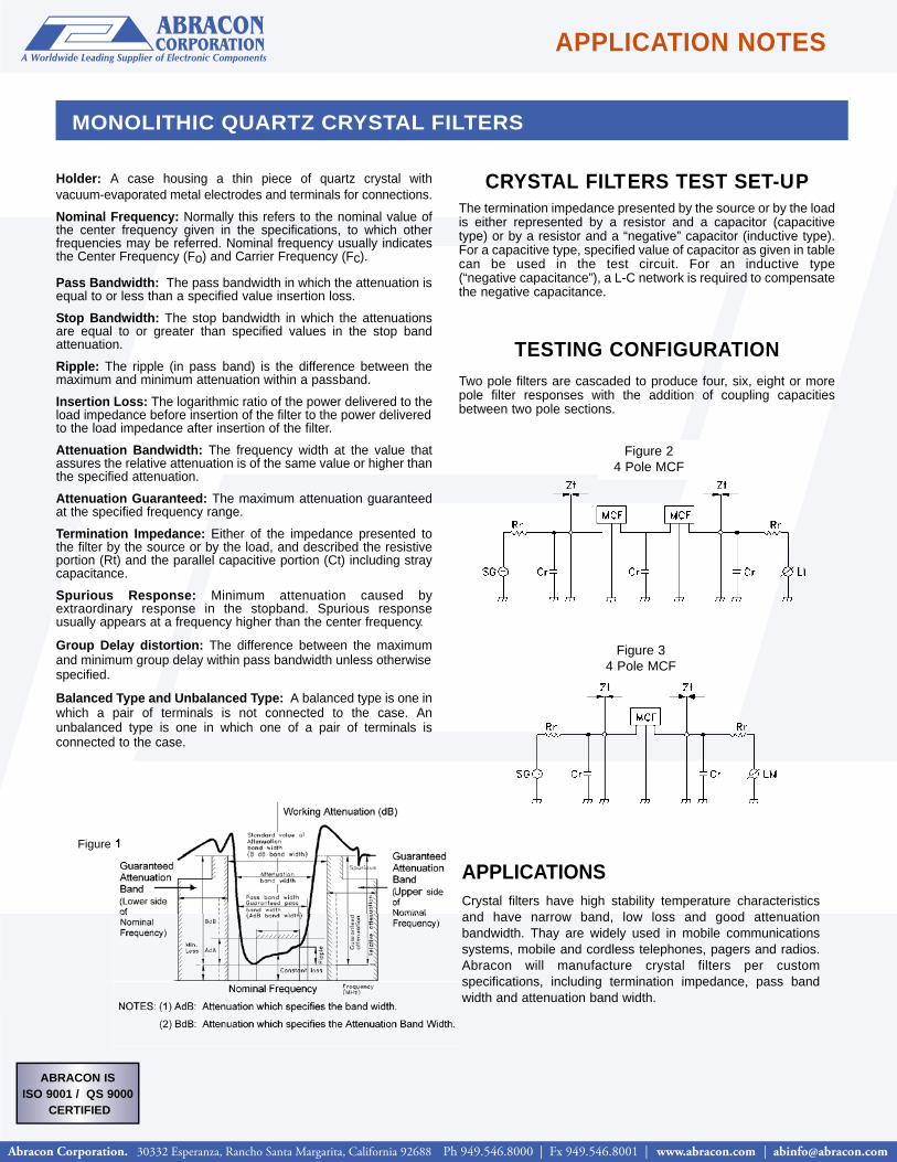
TESTING CONFIGURATIONTwo pole filters are cascaded to produce four, six, eight or morepole filter responses with the addition of coupling capacitiesbetween two pole sections.
APPLICATIONSCrystal filters have high stability temperature characteristicsand have narrow band, low loss and good attenuationbandwidth. Thay are widely used in mobile communicationssystems, mobile and cordless telephones, pagers and radios.Abracon will manufacture crystal filters per customspecifications, including termination impedance, pass bandwidth and attenuation band width.
Figure 24 Pole MCF
Figure 34 Pole MCF