Embed Size (px)
Citation preview
8-bit Microcontroller with 2K/4K Bytes In-SystemProgrammable Flash
ATtiny24AATtiny44A
Appendix A
Rev. 8183D-Appendix A–AVR–08/11
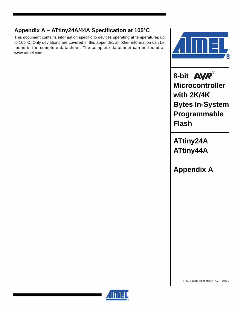
Appendix A – ATtiny24A/44A Specification at 105°CThis document contains information specific to devices operating at temperatures upto 105°C. Only deviations are covered in this appendix, all other information can befound in the complete datasheet. The complete datasheet can be found atwww.atmel.com.
1. Memories
1.1 EEPROM Data MemoryThe EEPROM has an endurance of at least 50,000 write/erase cycles.
28183D-Appendix A–AVR–08/11
ATtiny24A/44A
ATtiny24A/44A
2. Electrical Characteristics
2.1 Absolute Maximum Ratings*
2.2 DC Characteristics
Operating Temperature.................................. -55°C to +125°C *NOTICE: Stresses beyond those listed under “Absolute Maximum Ratings” may cause permanent dam-age to the device. This is a stress rating only and functional operation of the device at these or other conditions beyond those indicated in the operational sections of this specification is not implied. Exposure to absolute maximum rating conditions for extended periods may affect device reliability.
Storage Temperature ..................................... -65°C to +150°C
Voltage on any Pin except RESETwith respect to Ground ................................-0.5V to VCC+0.5V
Voltage on RESET with respect to Ground......-0.5V to +13.0V
Maximum Operating Voltage ............................................ 6.0V
DC Current per I/O Pin ............................................... 40.0 mA
DC Current VCC and GND Pins ................................ 200.0 mA
Table 2-1. DC Characteristics. TA = -40°C to +105°C
Symbol Parameter Condition Min Typ(1) Max Units
VIL
Input Low VoltageVCC = 1.8V - 2.4V -0.5 0.2VCC
(3) V
VCC = 2.4V - 5.5V -0.5 0.3VCC(3) V
Input Low Voltage,RESET Pin as Reset (4) VCC = 1.8V - 5.5 -0.5 0.2VCC
(3)
VIH
Input High-voltageExcept RESET pin
VCC = 1.8V - 2.4V 0.7VCC(2) VCC +0.5 V
VCC = 2.4V - 5.5V 0.6VCC(2) VCC +0.5 V
Input High-voltageRESET pin as Reset (4) VCC = 1.8V to 5.5V 0.9VCC
(2) VCC +0.5 V
VOLOutput Low Voltage(5)
Except RESET pin(7)
IOL = 10 mA, VCC = 5V 0.6 V
IOL = 5 mA, VCC = 3V 0.5 V
VOHOutput High-voltage(6)
Except RESET pin(7)
IOH = -10 mA, VCC = 5V 4.3 V
IOH = -5 mA, VCC = 3V 2.5 V
ILILInput LeakageCurrent I/O Pin
Vcc = 5.5V, pin low(absolute value)
< 0.05 1 (8) µA
ILIHInput LeakageCurrent I/O Pin
Vcc = 5.5V, pin high(absolute value)
< 0.05 1 (8) µA
RPU
Pull-up Resistor, I/O Pin VCC = 5.5V, input low 20 50 kΩ
Pull-up Resistor, Reset Pin VCC = 5.5V, input low 30 60 kΩ
38183D-Appendix A–AVR–08/11
Notes: 1. Typical values at 25°C.
2. “Min” means the lowest value where the pin is guaranteed to be read as high.
3. “Max” means the highest value where the pin is guaranteed to be read as low.
4. Not tested in production.
5. Although each I/O port can sink more than the test conditions (10 mA at VCC = 5V, 5 mA at VCC = 3V) under steady state conditions (non-transient), the sum of all IOL (for all ports) should not exceed 60 mA. If IOL exceeds the test conditions, VOL may exceed the related specification. Pins are not guaranteed to sink current greater than the listed test condition.
6. Although each I/O port can source more than the test conditions (10 mA at VCC = 5V, 5 mA at VCC = 3V) under steady state conditions (non-transient), the sum of all IOH (for all ports) should not exceed 60 mA. If IOH exceeds the test condition, VOH may exceed the related specification. Pins are not guaranteed to source current greater than the listed test condition.
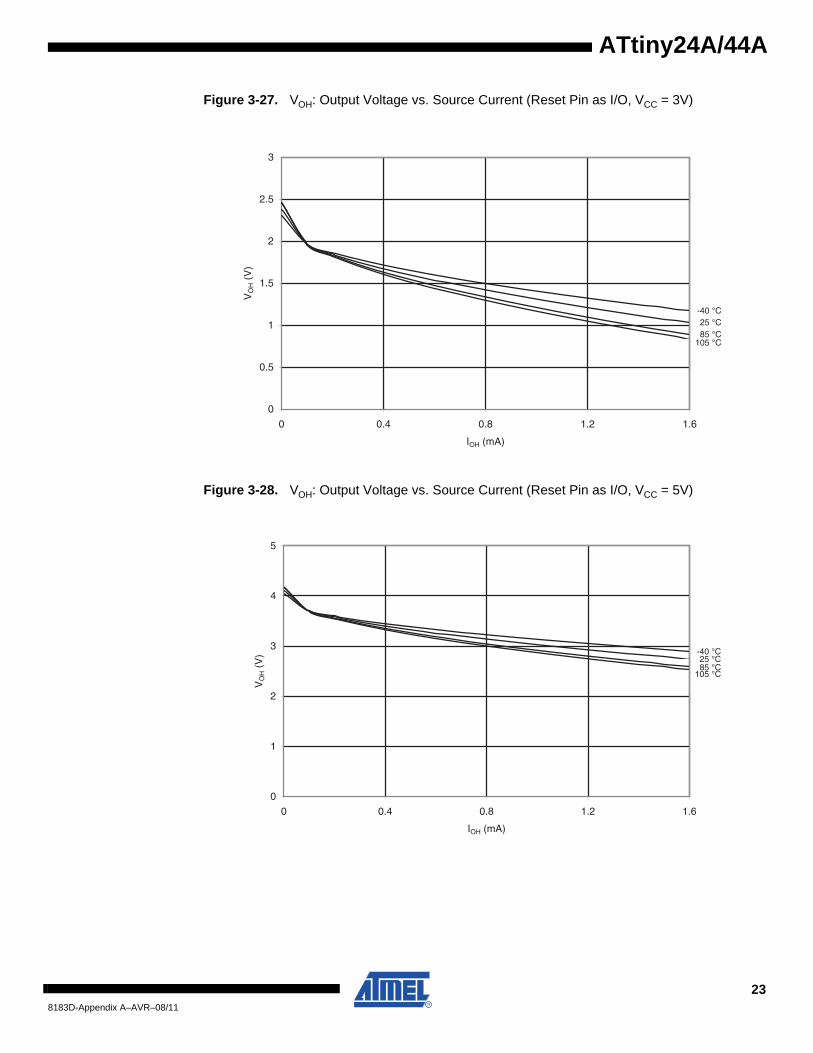
7. The RESET pin must tolerate high voltages when entering and operating in programming modes and, as a consequence, has a weak drive strength as compared to regular I/O pins. See Figure 3-25, Figure 3-26, Figure 3-27, and Figure 3-28 (starting on page 22).
8. These are test limits, which account for leakage currents of the test environment. Actual device leakage currents are lower.
9. Values are with external clock using methods described in “Minimizing Power Consumption”. Power reduction is enabled (PRR = 0xFF) and there is no I/O drive.
10. BOD disabled.
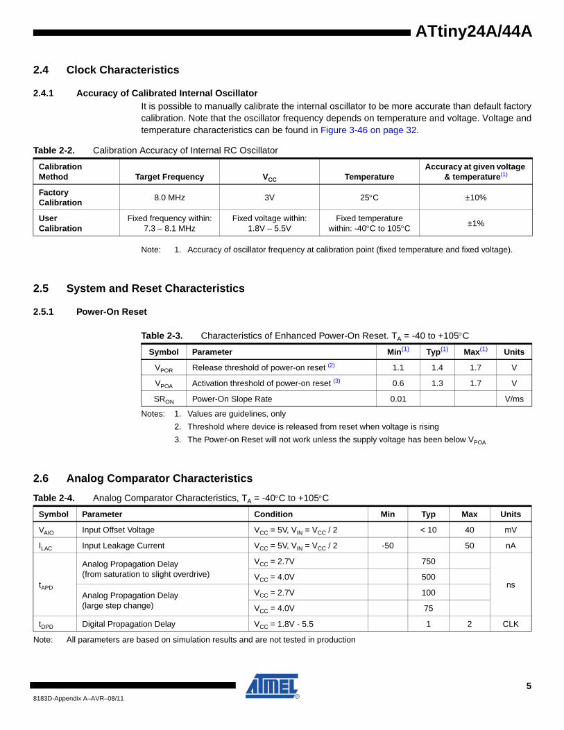
2.3 SpeedThe maximum operating frequency of the device depends on VCC. As shown in Figure 2-1, therelationship between maximum frequency and VCC is linear in the region 1.8V < VCC < 4.5V.
Figure 2-1. Maximum Frequency vs. VCC. TA = -40°C to +105°C
ICC
Supply Current,Active Mode (9)
f = 1MHz, VCC = 2V 0.25 0.5 mA
f = 4MHz, VCC = 3V 1.2 2 mA
f = 8MHz, VCC = 5V 4.4 7 mA
Supply Current,Idle Mode (9)
f = 1MHz, VCC = 2V 0.04 0.2 mA
f = 4MHz, VCC = 3V 0.25 0.6 mA
f = 8MHz, VCC = 5V 1.3 2 mA
Supply Current,Power-Down Mode (10)
WDT enabled, VCC = 3V 4 20 µA
WDT disabled, VCC = 3V 0.2 10 µA
Table 2-1. DC Characteristics. TA = -40°C to +105°C (Continued)
Symbol Parameter Condition Min Typ(1) Max Units
4 MHz
1.8V 5.5V4.5V
20 MHz
48183D-Appendix A–AVR–08/11
ATtiny24A/44A
ATtiny24A/44A
2.4 Clock Characteristics
2.4.1 Accuracy of Calibrated Internal OscillatorIt is possible to manually calibrate the internal oscillator to be more accurate than default factorycalibration. Note that the oscillator frequency depends on temperature and voltage. Voltage andtemperature characteristics can be found in Figure 3-46 on page 32.
Note: 1. Accuracy of oscillator frequency at calibration point (fixed temperature and fixed voltage).
2.5 System and Reset Characteristics
2.5.1 Power-On Reset
Notes: 1. Values are guidelines, only
2. Threshold where device is released from reset when voltage is rising
3. The Power-on Reset will not work unless the supply voltage has been below VPOA
2.6 Analog Comparator Characteristics
Note: All parameters are based on simulation results and are not tested in production
Table 2-2. Calibration Accuracy of Internal RC Oscillator
CalibrationMethod Target Frequency VCC Temperature
Accuracy at given voltage & temperature(1)
FactoryCalibration
8.0 MHz 3V 25°C ±10%
UserCalibration
Fixed frequency within:7.3 – 8.1 MHz
Fixed voltage within:1.8V – 5.5V
Fixed temperature within: -40°C to 105°C ±1%
Table 2-3. Characteristics of Enhanced Power-On Reset. TA = -40 to +105°C
Symbol Parameter Min(1) Typ(1) Max(1) Units
VPOR Release threshold of power-on reset (2) 1.1 1.4 1.7 V
VPOA Activation threshold of power-on reset (3) 0.6 1.3 1.7 V
SRON Power-On Slope Rate 0.01 V/ms
Table 2-4. Analog Comparator Characteristics, TA = -40°C to +105°C
Symbol Parameter Condition Min Typ Max Units
VAIO Input Offset Voltage VCC = 5V, VIN = VCC / 2 < 10 40 mV
ILAC Input Leakage Current VCC = 5V, VIN = VCC / 2 -50 50 nA
tAPD
Analog Propagation Delay(from saturation to slight overdrive)
VCC = 2.7V 750
nsVCC = 4.0V 500
Analog Propagation Delay(large step change)
VCC = 2.7V 100
VCC = 4.0V 75
tDPD Digital Propagation Delay VCC = 1.8V - 5.5 1 2 CLK
58183D-Appendix A–AVR–08/11
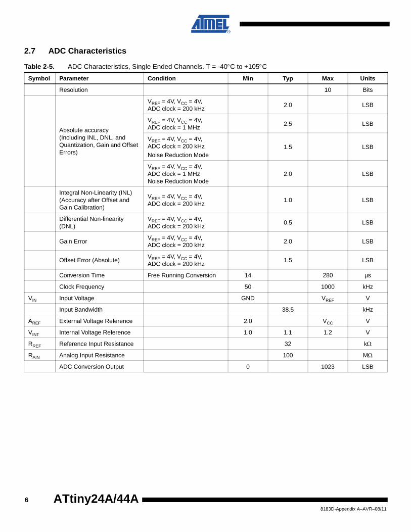
2.7 ADC Characteristics
Table 2-5. ADC Characteristics, Single Ended Channels. T = -40°C to +105°C
Symbol Parameter Condition Min Typ Max Units
Resolution 10 Bits
Absolute accuracy(Including INL, DNL, and Quantization, Gain and Offset Errors)
VREF = 4V, VCC = 4V,ADC clock = 200 kHz
2.0 LSB
VREF = 4V, VCC = 4V,ADC clock = 1 MHz
2.5 LSB
VREF = 4V, VCC = 4V,ADC clock = 200 kHz
Noise Reduction Mode1.5 LSB
VREF = 4V, VCC = 4V,ADC clock = 1 MHzNoise Reduction Mode
2.0 LSB
Integral Non-Linearity (INL)(Accuracy after Offset and Gain Calibration)
VREF = 4V, VCC = 4V,ADC clock = 200 kHz
1.0 LSB
Differential Non-linearity (DNL)
VREF = 4V, VCC = 4V,ADC clock = 200 kHz
0.5 LSB
Gain ErrorVREF = 4V, VCC = 4V,ADC clock = 200 kHz
2.0 LSB
Offset Error (Absolute)VREF = 4V, VCC = 4V,ADC clock = 200 kHz
1.5 LSB
Conversion Time Free Running Conversion 14 280 µs
Clock Frequency 50 1000 kHz
VIN Input Voltage GND VREF V
Input Bandwidth 38.5 kHz
AREF External Voltage Reference 2.0 VCC V
VINT Internal Voltage Reference 1.0 1.1 1.2 V
RREF Reference Input Resistance 32 kΩ
RAIN Analog Input Resistance 100 MΩ
ADC Conversion Output 0 1023 LSB
68183D-Appendix A–AVR–08/11
ATtiny24A/44A
ATtiny24A/44A
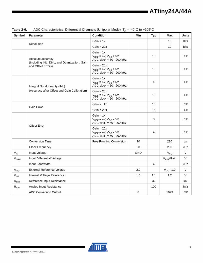
Table 2-6. ADC Characteristics, Differential Channels (Unipolar Mode), TA = -40°C to +105°C
Symbol Parameter Condition Min Typ Max Units
ResolutionGain = 1x 10 Bits
Gain = 20x 10 Bits
Absolute accuracy(Including INL, DNL, and Quantization, Gain and Offset Errors)
Gain = 1xVREF = 4V, VCC = 5VADC clock = 50 - 200 kHz
10 LSB
Gain = 20xVREF = 4V, VCC = 5VADC clock = 50 - 200 kHz
15 LSB
Integral Non-Linearity (INL)
(Accuracy after Offset and Gain Calibration)
Gain = 1xVREF = 4V, VCC = 5VADC clock = 50 - 200 kHz
4 LSB
Gain = 20xVREF = 4V, VCC = 5VADC clock = 50 - 200 kHz
10 LSB
Gain ErrorGain = 1x 10 LSB
Gain = 20x 15 LSB
Offset Error
Gain = 1xVREF = 4V, VCC = 5VADC clock = 50 - 200 kHz
3 LSB
Gain = 20xVREF = 4V, VCC = 5VADC clock = 50 - 200 kHz
4 LSB
Conversion Time Free Running Conversion 70 280 µs
Clock Frequency 50 200 kHz
VIN Input Voltage GND VCC V
VDIFF Input Differential Voltage VREF/Gain V
Input Bandwidth 4 kHz
AREF External Reference Voltage 2.0 VCC - 1.0 V
VINT Internal Voltage Reference 1.0 1.1 1.2 V
RREF Reference Input Resistance 32 kΩ
RAIN Analog Input Resistance 100 MΩ
ADC Conversion Output 0 1023 LSB
78183D-Appendix A–AVR–08/11
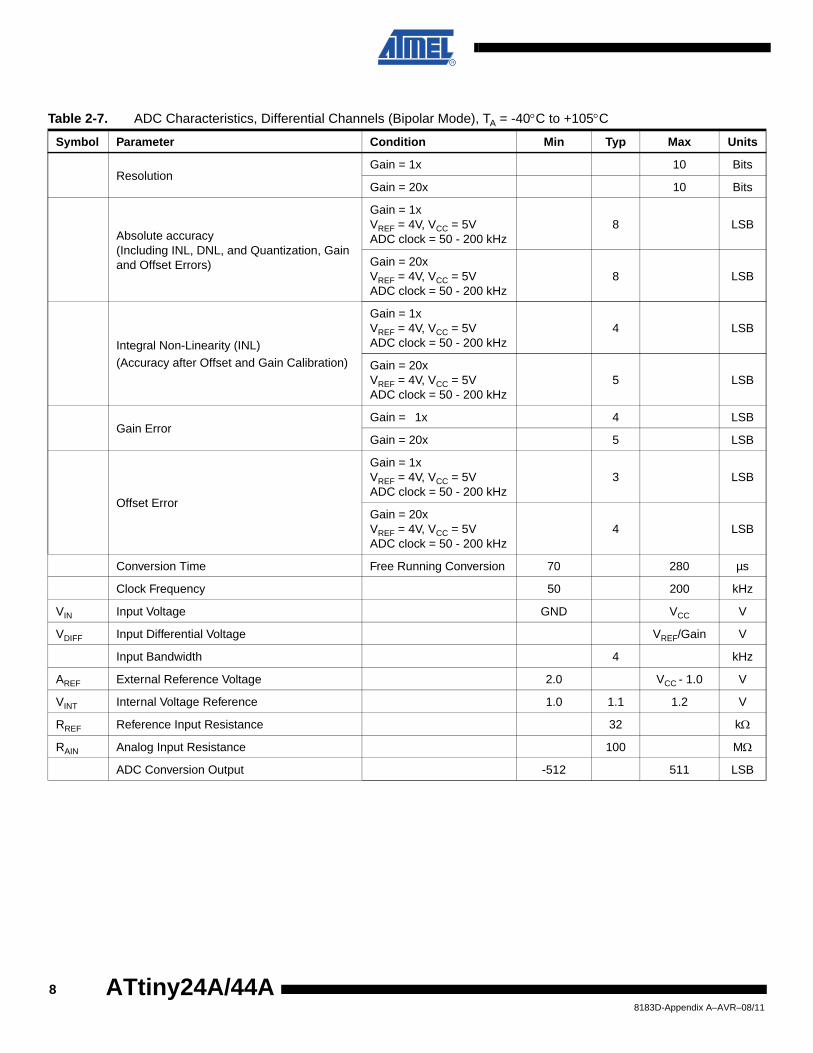
Table 2-7. ADC Characteristics, Differential Channels (Bipolar Mode), TA = -40°C to +105°C
Symbol Parameter Condition Min Typ Max Units
ResolutionGain = 1x 10 Bits
Gain = 20x 10 Bits
Absolute accuracy(Including INL, DNL, and Quantization, Gain and Offset Errors)
Gain = 1xVREF = 4V, VCC = 5VADC clock = 50 - 200 kHz
8 LSB
Gain = 20xVREF = 4V, VCC = 5VADC clock = 50 - 200 kHz
8 LSB
Integral Non-Linearity (INL)
(Accuracy after Offset and Gain Calibration)
Gain = 1xVREF = 4V, VCC = 5VADC clock = 50 - 200 kHz
4 LSB
Gain = 20xVREF = 4V, VCC = 5VADC clock = 50 - 200 kHz
5 LSB
Gain ErrorGain = 1x 4 LSB
Gain = 20x 5 LSB
Offset Error
Gain = 1xVREF = 4V, VCC = 5VADC clock = 50 - 200 kHz
3 LSB
Gain = 20xVREF = 4V, VCC = 5VADC clock = 50 - 200 kHz
4 LSB
Conversion Time Free Running Conversion 70 280 µs
Clock Frequency 50 200 kHz
VIN Input Voltage GND VCC V
VDIFF Input Differential Voltage VREF/Gain V
Input Bandwidth 4 kHz
AREF External Reference Voltage 2.0 VCC - 1.0 V
VINT Internal Voltage Reference 1.0 1.1 1.2 V
RREF Reference Input Resistance 32 kΩ
RAIN Analog Input Resistance 100 MΩ
ADC Conversion Output -512 511 LSB
88183D-Appendix A–AVR–08/11
ATtiny24A/44A
ATtiny24A/44A
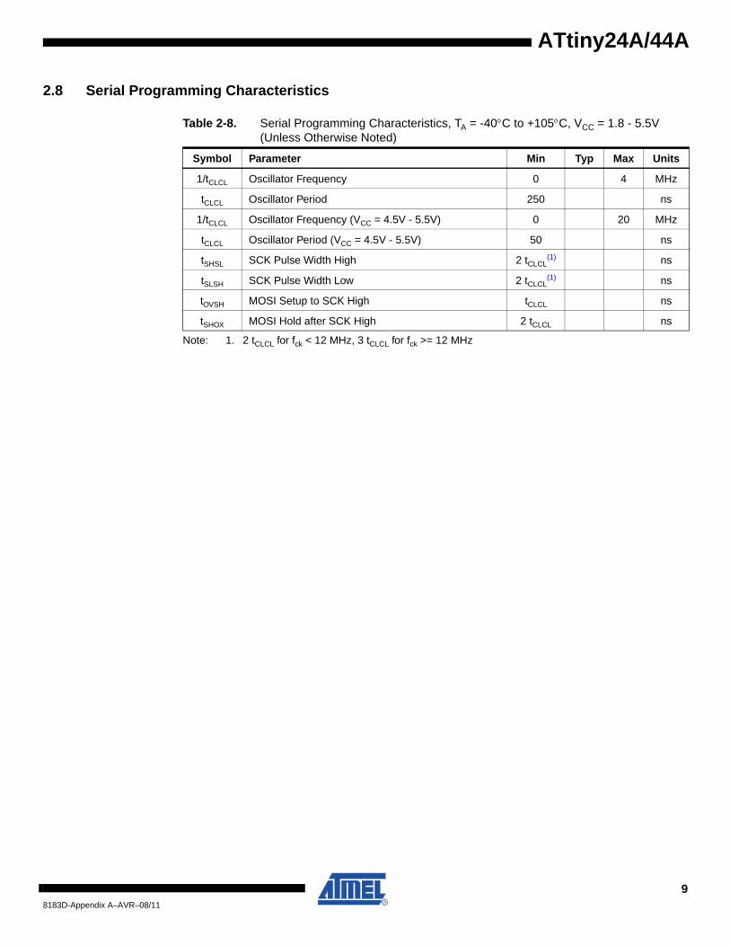
2.8 Serial Programming Characteristics
Note: 1. 2 tCLCL for fck < 12 MHz, 3 tCLCL for fck >= 12 MHz
Table 2-8. Serial Programming Characteristics, TA = -40°C to +105°C, VCC = 1.8 - 5.5V (Unless Otherwise Noted)
Symbol Parameter Min Typ Max Units
1/tCLCL Oscillator Frequency 0 4 MHz
tCLCL Oscillator Period 250 ns
1/tCLCL Oscillator Frequency (VCC = 4.5V - 5.5V) 0 20 MHz
tCLCL Oscillator Period (VCC = 4.5V - 5.5V) 50 ns
tSHSL SCK Pulse Width High 2 tCLCL(1) ns
tSLSH SCK Pulse Width Low 2 tCLCL(1) ns
tOVSH MOSI Setup to SCK High tCLCL ns
tSHOX MOSI Hold after SCK High 2 tCLCL ns
98183D-Appendix A–AVR–08/11
3. Typical Characteristics
3.1 ATtiny24A
3.1.1 Current Consumption in Active Mode
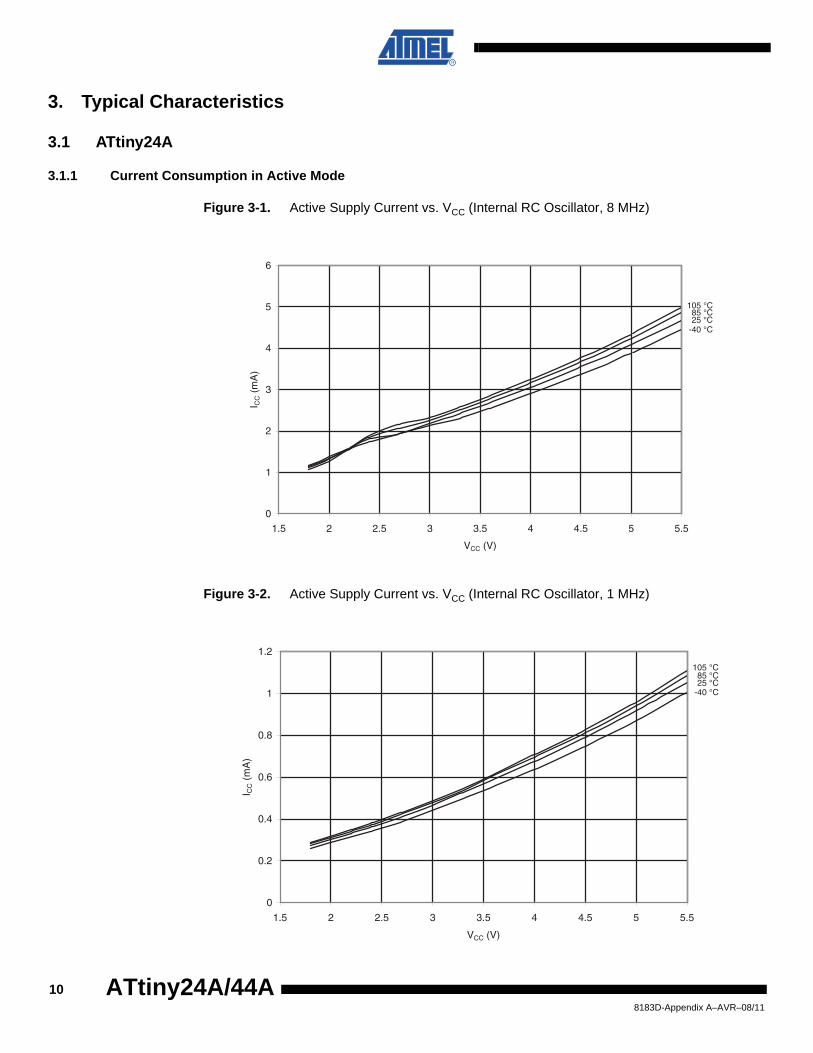
Figure 3-1. Active Supply Current vs. VCC (Internal RC Oscillator, 8 MHz)
Figure 3-2. Active Supply Current vs. VCC (Internal RC Oscillator, 1 MHz)
105 °C85 °C25 °C
-40 °C
0
1
2
3
4
5
6
1.5 2 2.5 3 3.5 4 4.5 5 5.5
VCC (V)
I CC (
mA
)
105 °C85 °C25 °C
-40 °C
0
0.2
0.4
0.6
0.8
1
1.2
1.5 2 2.5 3 3.5 4 4.5 5 5.5
VCC (V)
I CC (
mA
)
108183D-Appendix A–AVR–08/11
ATtiny24A/44A
ATtiny24A/44A
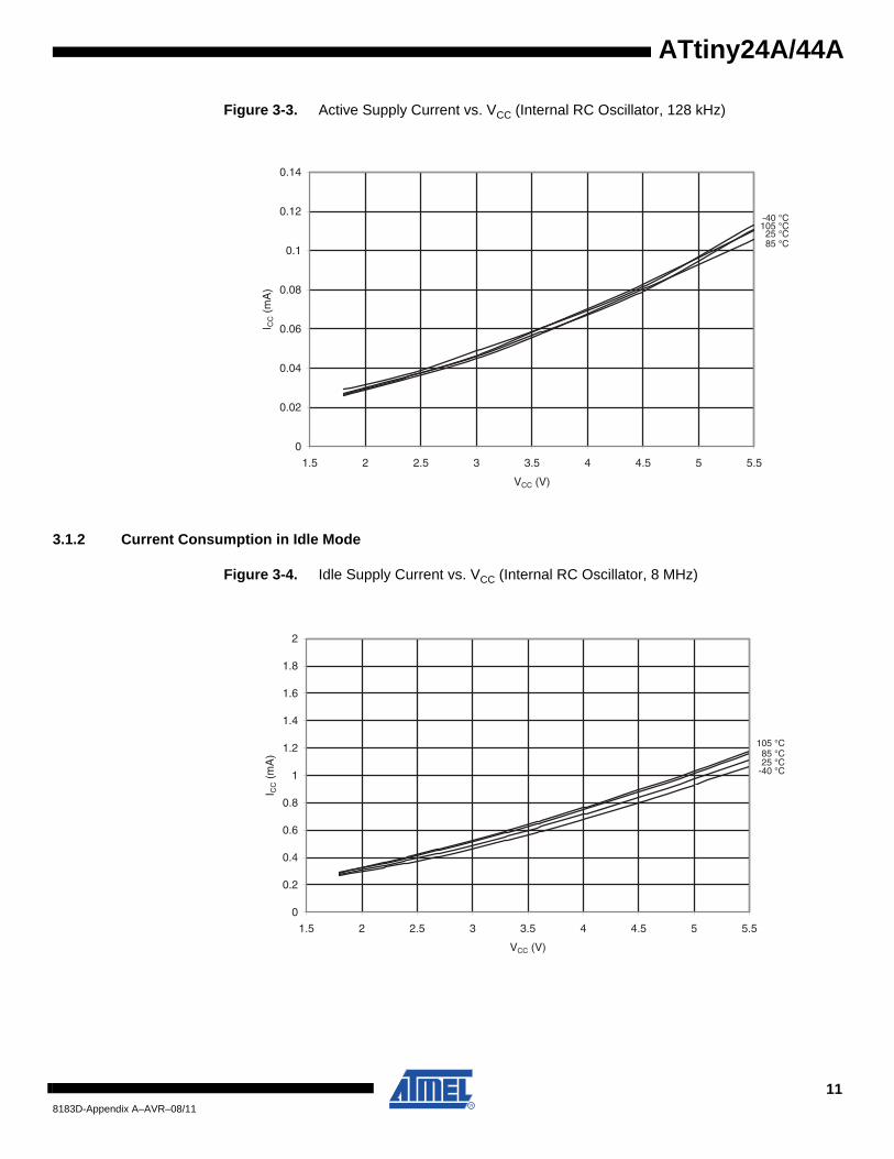
Figure 3-3. Active Supply Current vs. VCC (Internal RC Oscillator, 128 kHz)
3.1.2 Current Consumption in Idle Mode
Figure 3-4. Idle Supply Current vs. VCC (Internal RC Oscillator, 8 MHz)
105 °C
85 °C25 °C
-40 °C
0
0.02
0.04
0.06
0.08
0.1
0.12
0.14
1.5 2 2.5 3 3.5 4 4.5 5 5.5
VCC (V)
I CC (
mA
)
105 °C85 °C25 °C
-40 °C
0
0.2
0.4
0.6
0.8
1
1.2
1.4
1.6
1.8
2
1.5 2 2.5 3 3.5 4 4.5 5 5.5
VCC (V)
I CC (
mA
)
118183D-Appendix A–AVR–08/11
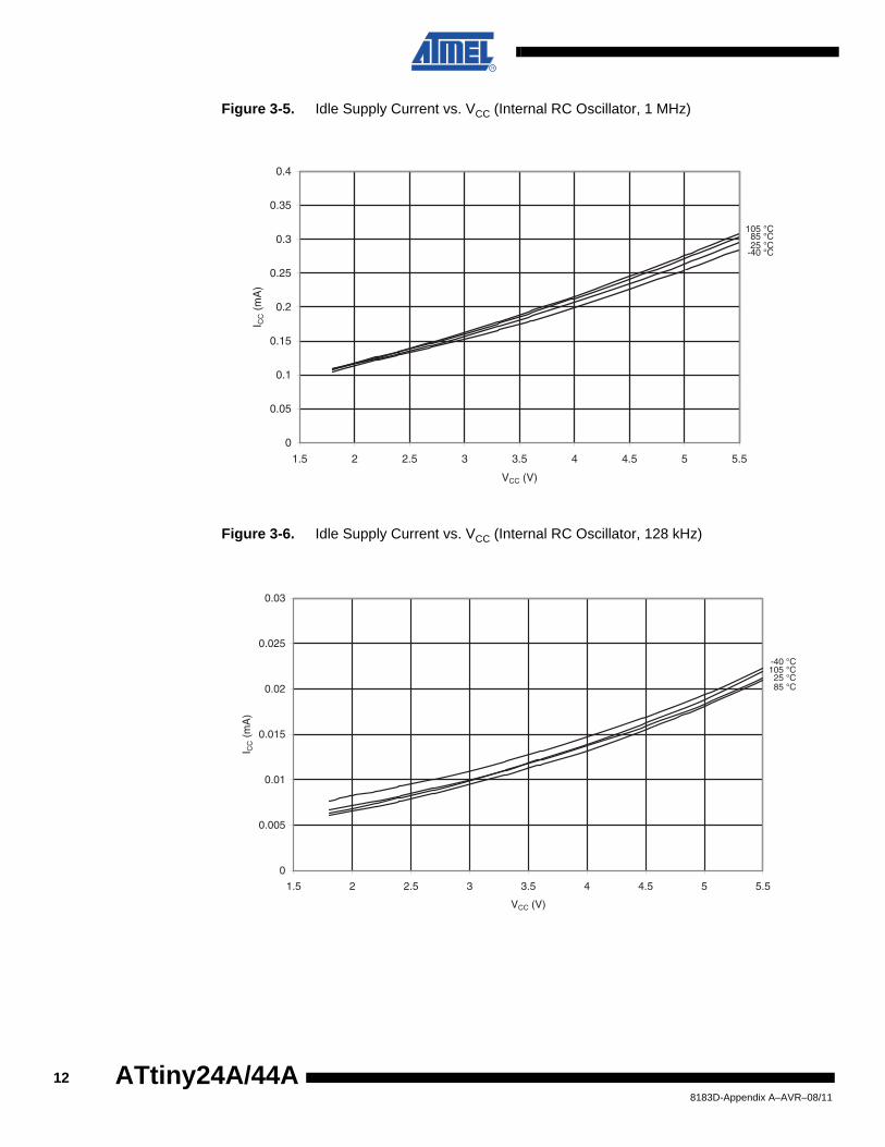
Figure 3-5. Idle Supply Current vs. VCC (Internal RC Oscillator, 1 MHz)
Figure 3-6. Idle Supply Current vs. VCC (Internal RC Oscillator, 128 kHz)
105 °C85 °C25 °C
-40 °C
0
0.05
0.1
0.15
0.2
0.25
0.3
0.35
0.4
1.5 2 2.5 3 3.5 4 4.5 5 5.5
VCC (V)
I CC (
mA
)
105 °C
85 °C25 °C
-40 °C
0
0.005
0.01
0.015
0.02
0.025
0.03
1.5 2 2.5 3 3.5 4 4.5 5 5.5
VCC (V)
I CC (
mA
)
128183D-Appendix A–AVR–08/11
ATtiny24A/44A
ATtiny24A/44A
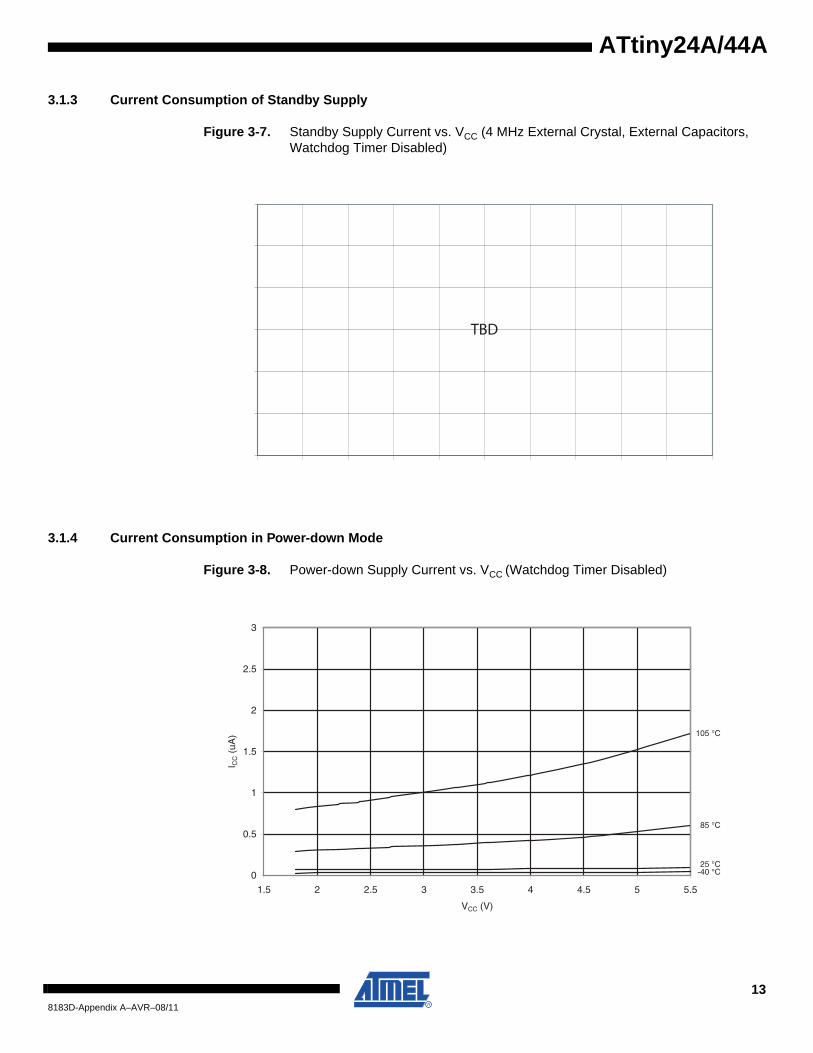
3.1.3 Current Consumption of Standby Supply
Figure 3-7. Standby Supply Current vs. VCC (4 MHz External Crystal, External Capacitors, Watchdog Timer Disabled)
3.1.4 Current Consumption in Power-down Mode
Figure 3-8. Power-down Supply Current vs. VCC (Watchdog Timer Disabled)
TBD
105 °C
85 °C
25 °C-40 °C0
0.5
1
1.5
2
2.5
3
1.5 2 2.5 3 3.5 4 4.5 5 5.5
VCC (V)
I CC (
uA)
138183D-Appendix A–AVR–08/11
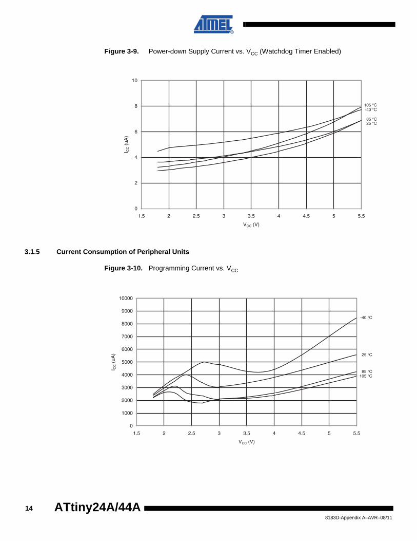
Figure 3-9. Power-down Supply Current vs. VCC (Watchdog Timer Enabled)
3.1.5 Current Consumption of Peripheral Units
Figure 3-10. Programming Current vs. VCC
105 °C
85 °C25 °C
-40 °C
0
2
4
6
8
10
1.5 2 2.5 3 3.5 4 4.5 5 5.5
VCC (V)
I CC (
uA)
105 °C85 °C
25 °C
-40 °C
0
1000
2000
3000
4000
5000
6000
7000
8000
9000
10000
1.5 2 2.5 3 3.5 4 4.5 5 5.5
VCC (V)
I CC (
uA)
148183D-Appendix A–AVR–08/11
ATtiny24A/44A
ATtiny24A/44A
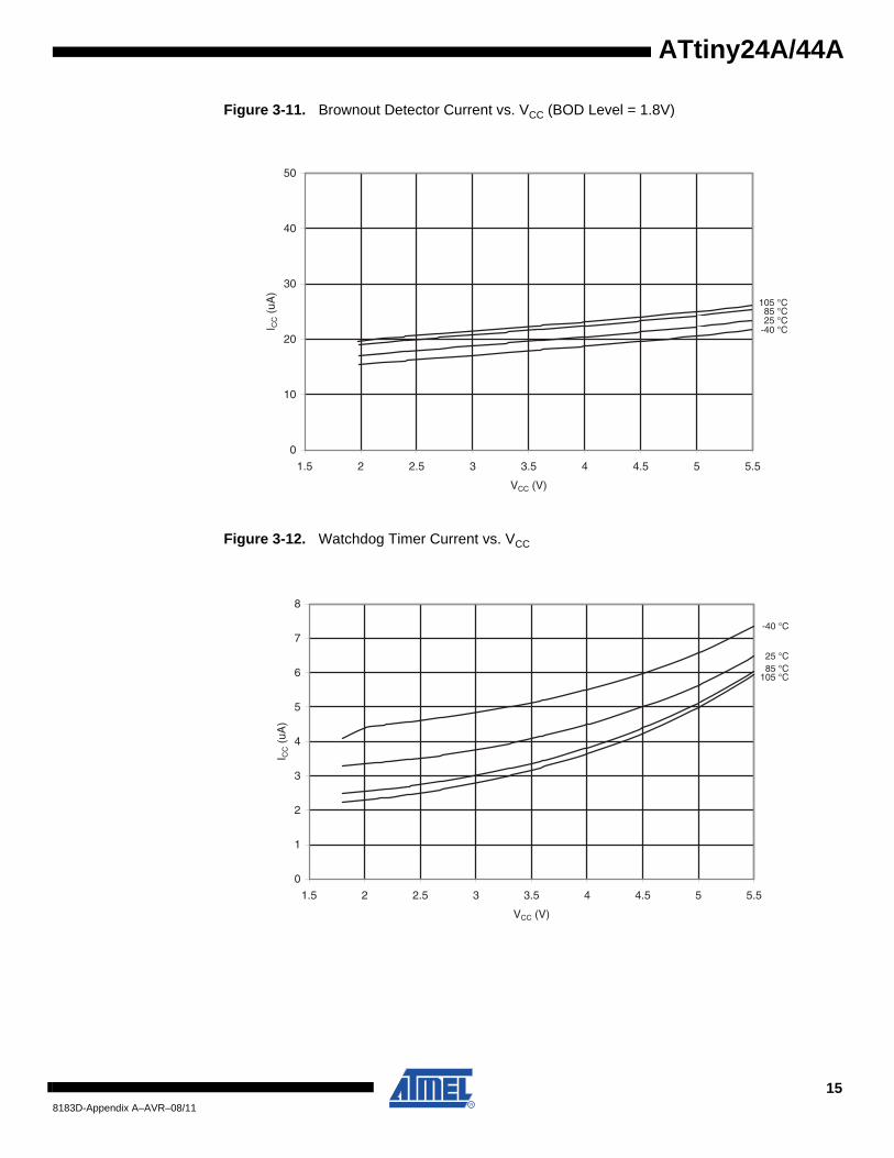
Figure 3-11. Brownout Detector Current vs. VCC (BOD Level = 1.8V)
Figure 3-12. Watchdog Timer Current vs. VCC
105 °C85 °C25 °C
-40 °C
0
10
20
30
40
50
1.5 2 2.5 3 3.5 4 4.5 5 5.5
VCC (V)
I CC (
uA)
105 °C85 °C25 °C
-40 °C
0
1
2
3
4
5
6
7
8
1.5 2 2.5 3 3.5 4 4.5 5 5.5
VCC (V)
I CC (
uA)
158183D-Appendix A–AVR–08/11
3.1.6 Pull-up Resistors
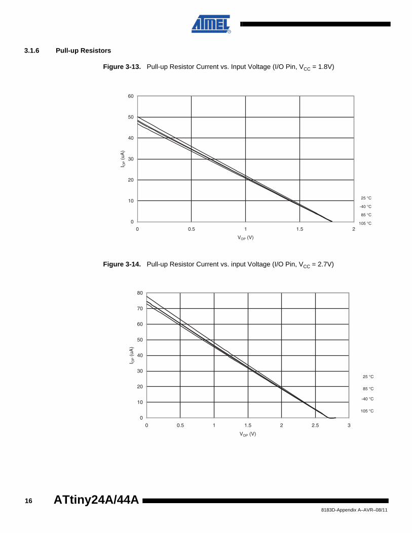
Figure 3-13. Pull-up Resistor Current vs. Input Voltage (I/O Pin, VCC = 1.8V)
Figure 3-14. Pull-up Resistor Current vs. input Voltage (I/O Pin, VCC = 2.7V)
105 °C
85 °C
25 °C
0
10
20
30
40
50
60
0 0.5 1 1.5 2
VOP (V)
I OP (
uA)
-40 °C
85 °C
25 °C
0
10
20
30
40
50
60
70
80
0 0.5 1 1.5 2 2.5 3
VOP (V)
I OP (
uA)
105 °C
-40 °C
168183D-Appendix A–AVR–08/11
ATtiny24A/44A
ATtiny24A/44A
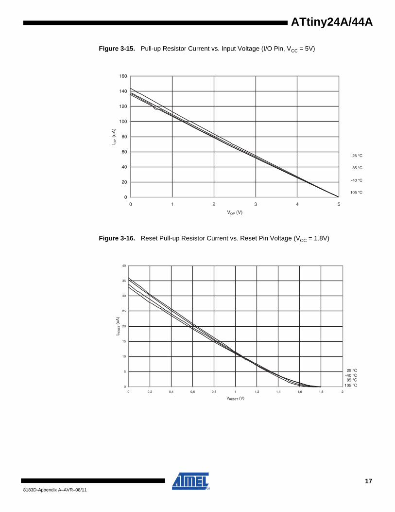
Figure 3-15. Pull-up Resistor Current vs. Input Voltage (I/O Pin, VCC = 5V)
Figure 3-16. Reset Pull-up Resistor Current vs. Reset Pin Voltage (VCC = 1.8V)
85 °C
25 °C
0
20
40
60
80
100
120
140
160
0 1 2 3 4 5
VOP (V)
I OP (
uA)
105 °C
-40 °C
105 °C85 °C
25 °C-40 °C
0
5
10
15
20
25
30
35
40
0 0,2 0,4 0,6 0,8 1 1,2 1,4 1,6 1,8 2
VRESET (V)
I RE
SE
T (
uA)
178183D-Appendix A–AVR–08/11
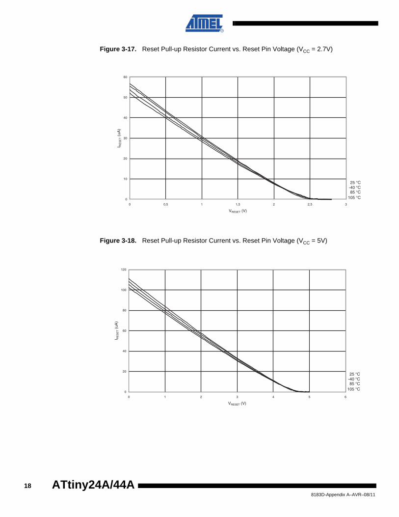
Figure 3-17. Reset Pull-up Resistor Current vs. Reset Pin Voltage (VCC = 2.7V)
Figure 3-18. Reset Pull-up Resistor Current vs. Reset Pin Voltage (VCC = 5V)
105 °C85 °C
25 °C-40 °C
0
10
20
30
40
50
60
35,225,115,00
VRESET (V)
I RE
SE
T (
uA)
105 °C85 °C
25 °C-40 °C
0
20
40
60
80
100
120
6543210
VRESET (V)
I RE
SE
T (
uA)
188183D-Appendix A–AVR–08/11
ATtiny24A/44A
ATtiny24A/44A
3.1.7 Output Driver Strength
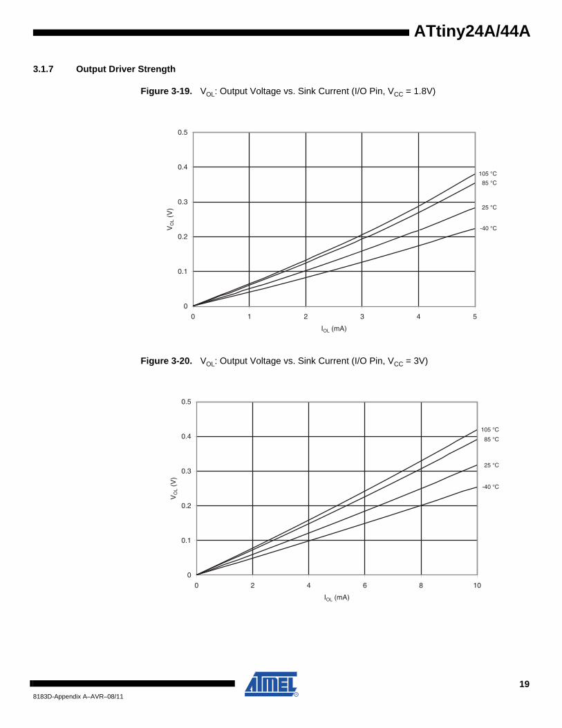
Figure 3-19. VOL: Output Voltage vs. Sink Current (I/O Pin, VCC = 1.8V)
Figure 3-20. VOL: Output Voltage vs. Sink Current (I/O Pin, VCC = 3V)
105 °C
85 °C
25 °C
-40 °C
0
0.1
0.2
0.3
0.4
0.5
0 1 2 3 4 5
IOL (mA)
VO
L (V
)
105 °C
85 °C
25 °C
-40 °C
0
0.1
0.2
0.3
0.4
0.5
0 2 4 6 8 10
IOL (mA)
VO
L (V
)
198183D-Appendix A–AVR–08/11
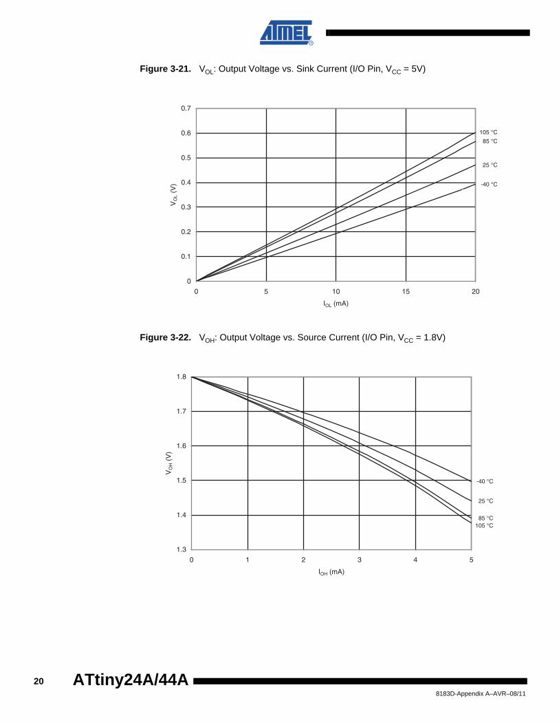
Figure 3-21. VOL: Output Voltage vs. Sink Current (I/O Pin, VCC = 5V)
Figure 3-22. VOH: Output Voltage vs. Source Current (I/O Pin, VCC = 1.8V)
105 °C
85 °C
25 °C
-40 °C
0
0.1
0.2
0.3
0.4
0.5
0.6
0.7
0 5 10 15 20
IOL (mA)
VO
L (V
)
105 °C85 °C
25 °C
-40 °C
1.3
1.4
1.5
1.6
1.7
1.8
0 1 2 3 4 5
IOH (mA)
VO
H (
V)
208183D-Appendix A–AVR–08/11
ATtiny24A/44A
ATtiny24A/44A
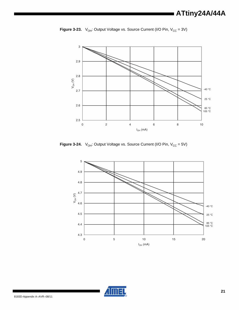
Figure 3-23. VOH: Output Voltage vs. Source Current (I/O Pin, VCC = 3V)
Figure 3-24. VOH: Output Voltage vs. Source Current (I/O Pin, VCC = 5V)
105 °C85 °C
25 °C
-40 °C
2.5
2.6
2.7
2.8
2.9
3
0 2 4 6 8 10
IOH (mA)
VO
H (
V)
105 °C85 °C
25 °C
-40 °C
4.3
4.4
4.5
4.6
4.7
4.8
4.9
5
0 5 10 15 20
IOH (mA)
VO
H (
V)
218183D-Appendix A–AVR–08/11
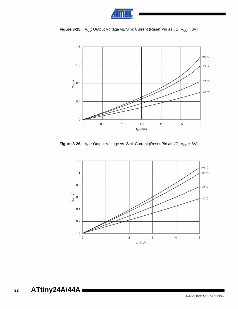
Figure 3-25. VOL: Output Voltage vs. Sink Current (Reset Pin as I/O, VCC = 3V)
Figure 3-26. VOL: Output Voltage vs. Sink Current (Reset Pin as I/O, VCC = 5V)
-40 °C
25 °C
85 °C
105 °C
0
0.4
0.8
1.2
1.6
0 0.5 1 1.5 2 2.5 3
IOL (mA)
VO
L (V
)
-40 °C
25 °C
85 °C
105 °C
0
0.2
0.4
0.6
0.8
1
1.2
0 1 2 3 4 5
IOL (mA)
VO
L (V
)
228183D-Appendix A–AVR–08/11
ATtiny24A/44A
ATtiny24A/44A
Figure 3-27. VOH: Output Voltage vs. Source Current (Reset Pin as I/O, VCC = 3V)
Figure 3-28. VOH: Output Voltage vs. Source Current (Reset Pin as I/O, VCC = 5V)
-40 °C25 °C85 °C
105 °C
0
0.5
1
1.5
2
2.5
3
0 0.4 0.8 1.2 1.6
IOH (mA)
VO
H (
V)
-40 °C25 °C85 °C
105 °C
0
1
2
3
4
5
0 0.4 0.8 1.2 1.6
IOH (mA)
VO
H (
V)
238183D-Appendix A–AVR–08/11
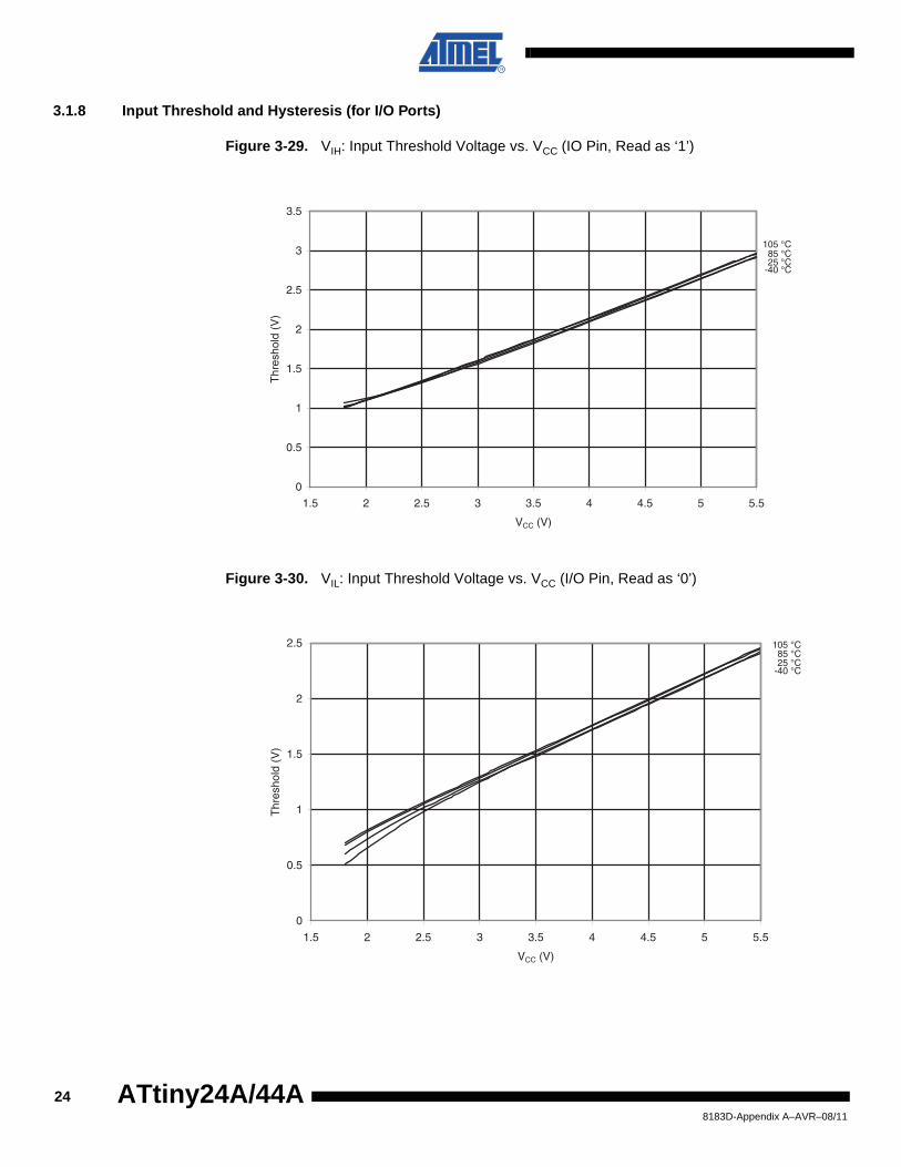
3.1.8 Input Threshold and Hysteresis (for I/O Ports)
Figure 3-29. VIH: Input Threshold Voltage vs. VCC (IO Pin, Read as ‘1’)
Figure 3-30. VIL: Input Threshold Voltage vs. VCC (I/O Pin, Read as ‘0’)
105 °C85 °C25 °C
-40 °C
0
0.5
1
1.5
2
2.5
3
3.5
1.5 2 2.5 3 3.5 4 4.5 5 5.5
VCC (V)
Thr
esho
ld (
V)
105 °C85 °C25 °C
-40 °C
0
0.5
1
1.5
2
2.5
1.5 2 2.5 3 3.5 4 4.5 5 5.5
VCC (V)
Thr
esho
ld (
V)
248183D-Appendix A–AVR–08/11
ATtiny24A/44A
ATtiny24A/44A
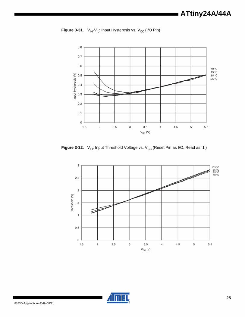
Figure 3-31. VIH-VIL: Input Hysteresis vs. VCC (I/O Pin)
Figure 3-32. VIH: Input Threshold Voltage vs. VCC (Reset Pin as I/O, Read as ‘1’)
105 °C85 °C25 °C
-40 °C
0
0.1
0.2
0.3
0.4
0.5
0.6
0.7
0.8
1.5 2 2.5 3 3.5 4 4.5 5 5.5
VCC (V)
Inpu
t Hys
tere
sis
(V)
105 °C85 °C25 °C
-40 °C
0
0.5
1
1.5
2
2.5
3
1.5 2 2.5 3 3.5 4 4.5 5 5.5
VCC (V)
Thr
esho
ld (
V)
258183D-Appendix A–AVR–08/11
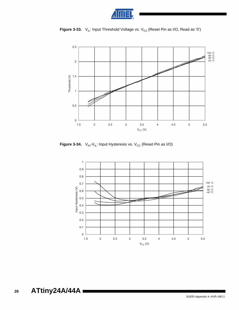
Figure 3-33. VIL: Input Threshold Voltage vs. VCC (Reset Pin as I/O, Read as ‘0’)
Figure 3-34. VIH-VIL: Input Hysteresis vs. VCC (Reset Pin as I/O)
85 °C
25 °C-40 °C
0
0.5
1
1.5
2
2.5
1.5 2 2.5 3 3.5 4 4.5 5 5.5
VCC (V)
Thr
esho
ld (
V)
105 °C
85 °C25 °C
-40 °C
0
0.1
0.2
0.3
0.4
0.5
0.6
0.7
0.8
0.9
1
1.5 2 2.5 3 3.5 4 4.5 5 5.5
VCC (V)
Inpu
t Hys
tere
sis
(V)
105 °C
268183D-Appendix A–AVR–08/11
ATtiny24A/44A
ATtiny24A/44A
3.1.9 BOD and Bandgap
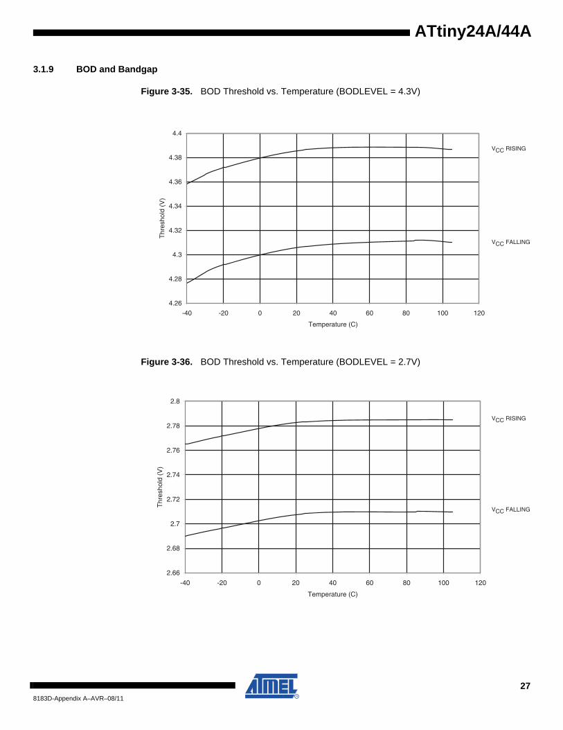
Figure 3-35. BOD Threshold vs. Temperature (BODLEVEL = 4.3V)
Figure 3-36. BOD Threshold vs. Temperature (BODLEVEL = 2.7V)
VCC RISING
VCC FALLING
4.26
4.28
4.3
4.32
4.34
4.36
4.38
4.4
-40 -20 0 20 40 60 80 100 120
Temperature (C)
Thr
esho
ld (
V)
VCC RISING
VCC FALLING
2.66
2.68
2.7
2.72
2.74
2.76
2.78
2.8
-40 -20 0 20 40 60 80 100 120
Temperature (C)
Thr
esho
ld (
V)
278183D-Appendix A–AVR–08/11
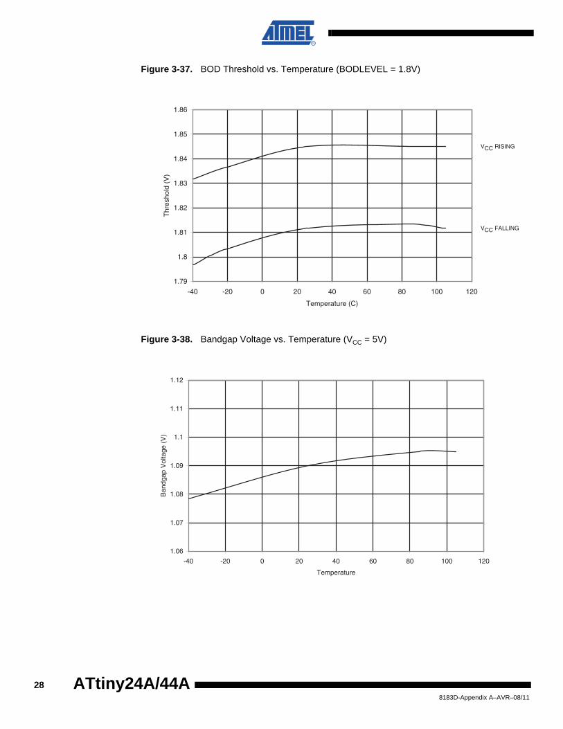
Figure 3-37. BOD Threshold vs. Temperature (BODLEVEL = 1.8V)
Figure 3-38. Bandgap Voltage vs. Temperature (VCC = 5V)
VCC RISING
VCC FALLING
1.79
1.8
1.81
1.82
1.83
1.84
1.85
1.86
-40 -20 0 20 40 60 80 100 120
Temperature (C)
Thr
esho
ld (
V)
1.06
1.07
1.08
1.09
1.1
1.11
1.12
-40 -20 0 20 40 60 80 100 120
Temperature
Ban
dgap
Vol
tage
(V
)
288183D-Appendix A–AVR–08/11
ATtiny24A/44A
ATtiny24A/44A
Figure 3-39. VIH: Input Threshold Voltage vs. VCC (Reset Pin, Read as ‘1’)
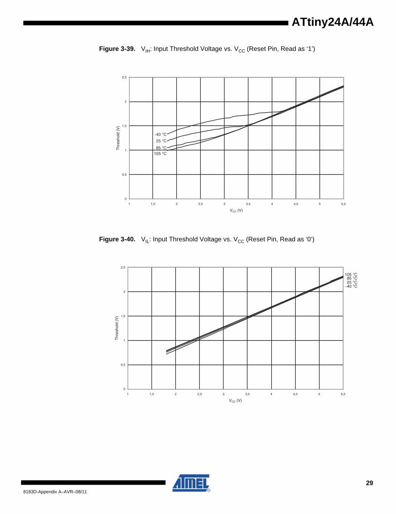
Figure 3-40. VIL: Input Threshold Voltage vs. VCC (Reset Pin, Read as ‘0’)
105 °C85 °C
25 °C
-40 °C
0
0,5
1
1,5
2
2,5
1 1,5 2 2,5 3 3,5 4 4,5 5 5,5
VCC (V)
Thr
esho
ld (
V)
105 °C85 °C25 °C
-40 °C
0
0,5
1
1,5
2
2,5
1 1,5 2 2,5 3 3,5 4 4,5 5 5,5
VCC (V)
Thr
esho
ld (
V)
298183D-Appendix A–AVR–08/11
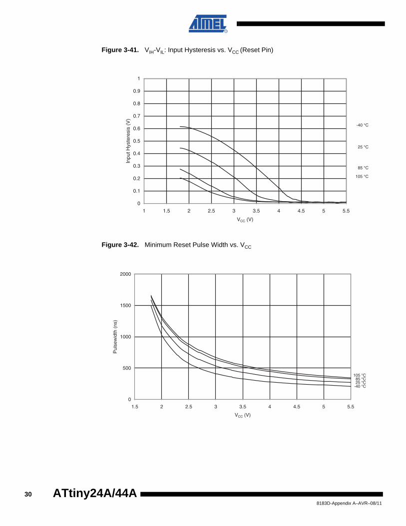
Figure 3-41. VIH-VIL: Input Hysteresis vs. VCC (Reset Pin)
Figure 3-42. Minimum Reset Pulse Width vs. VCC
105 °C
85 °C
25 °C
-40 °C
0
0.1
0.2
0.3
0.4
0.5
0.6
0.7
0.8
0.9
1
1 1.5 2 2.5 3 3.5 4 4.5 5 5.5
VCC (V)
Inpu
t Hys
tere
sis
(V)
105 °C85 °C25 °C
-40 °C
0
500
1000
1500
2000
1.5 2 2.5 3 3.5 4 4.5 5 5.5
VCC (V)
Pul
sew
idth
(ns
)
308183D-Appendix A–AVR–08/11
ATtiny24A/44A
ATtiny24A/44A
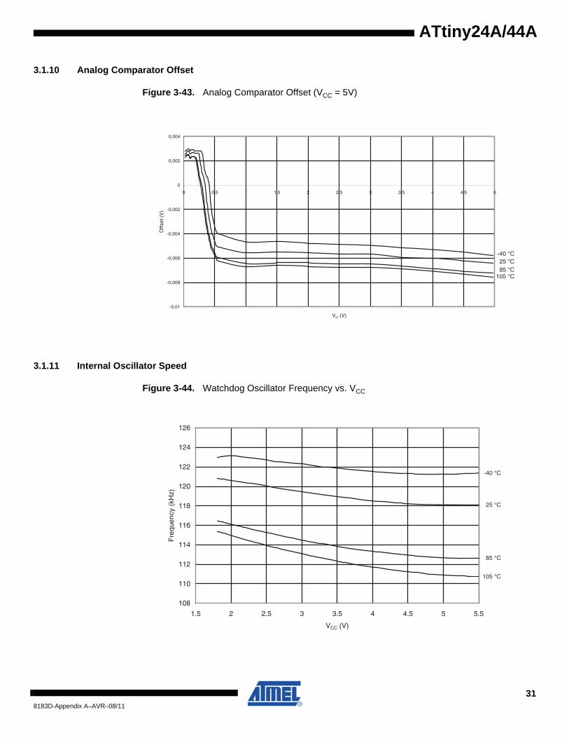
3.1.10 Analog Comparator Offset
Figure 3-43. Analog Comparator Offset (VCC = 5V)
3.1.11 Internal Oscillator Speed
Figure 3-44. Watchdog Oscillator Frequency vs. VCC
105 °C85 °C25 °C
-40 °C
-0,01
-0,008
-0,006
-0,004
-0,002
0
0,002
0,004
0 0,5 1 1,5 2 2,5 3 3,5 4 4,5 5
Vin (V)
Offs
et (
V)
105 °C
85 °C
25 °C
-40 °C
108
110
112
114
116
118
120
122
124
126
1.5 2 2.5 3 3.5 4 4.5 5 5.5
VCC (V)
Fre
quen
cy (
kHz)
318183D-Appendix A–AVR–08/11
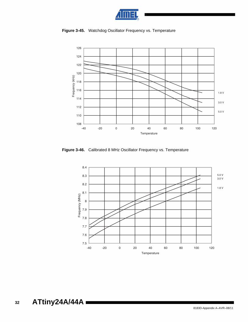
Figure 3-45. Watchdog Oscillator Frequency vs. Temperature
Figure 3-46. Calibrated 8 MHz Oscillator Frequency vs. Temperature
5.0 V
3.0 V
1.8 V
108
110
112
114
116
118
120
122
124
126
-40 -20 0 20 40 60 80 100 120
Temperature
Fre
quen
cy (
kHz)
5.0 V3.0 V
1.8 V
7.5
7.6
7.7
7.8
7.9
8
8.1
8.2
8.3
8.4
-40 -20 0 20 40 60 80 100 120
Temperature
Fre
quen
cy (
MH
z)
328183D-Appendix A–AVR–08/11
ATtiny24A/44A
ATtiny24A/44A
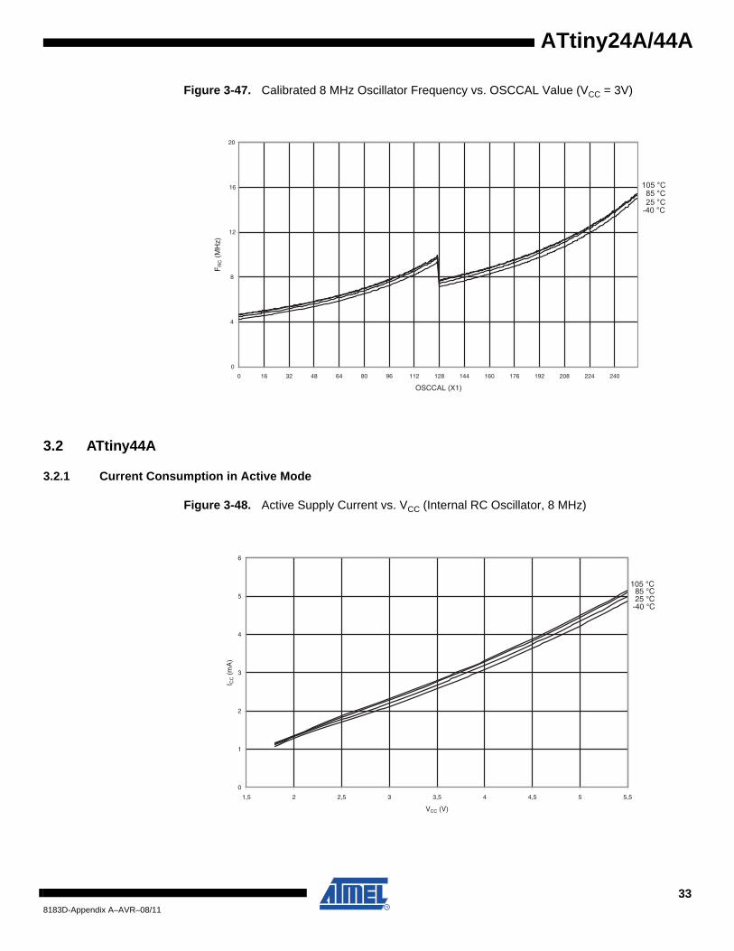
Figure 3-47. Calibrated 8 MHz Oscillator Frequency vs. OSCCAL Value (VCC = 3V)
3.2 ATtiny44A
3.2.1 Current Consumption in Active Mode
Figure 3-48. Active Supply Current vs. VCC (Internal RC Oscillator, 8 MHz)
105 °C85 °C25 °C
-40 °C
0
4
8
12
16
20
0 16 32 48 64 80 96 112 128 144 160 176 192 208 224 240
OSCCAL (X1)
FR
C (
MH
z)
105 °C85 °C25 °C
-40 °C
0
1
2
3
4
5
6
1,5 2 2,5 3 3,5 4 4,5 5 5,5
VCC (V)
I CC (
mA
)
338183D-Appendix A–AVR–08/11
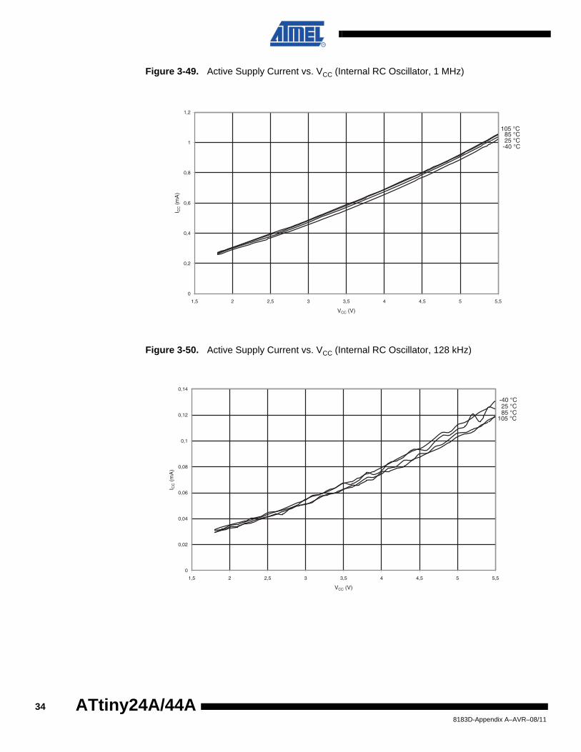
Figure 3-49. Active Supply Current vs. VCC (Internal RC Oscillator, 1 MHz)
Figure 3-50. Active Supply Current vs. VCC (Internal RC Oscillator, 128 kHz)
105 °C85 °C25 °C
-40 °C
0
0,2
0,4
0,6
0,8
1
1,2
1,5 2 2,5 3 3,5 4 4,5 5 5,5
VCC (V)
I CC (
mA
)
105 °C85 °C25 °C
-40 °C
0
0,02
0,04
0,06
0,08
0,1
0,12
0,14
1,5 2 2,5 3 3,5 4 4,5 5 5,5
VCC (V)
I CC (
mA
)
348183D-Appendix A–AVR–08/11
ATtiny24A/44A
ATtiny24A/44A
3.2.2 Current Consumption in Idle Mode
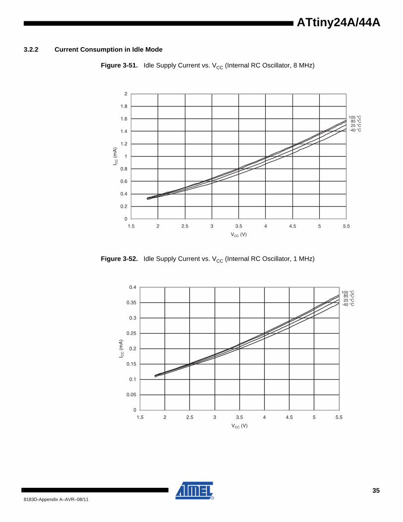
Figure 3-51. Idle Supply Current vs. VCC (Internal RC Oscillator, 8 MHz)
Figure 3-52. Idle Supply Current vs. VCC (Internal RC Oscillator, 1 MHz)
105 °C85 °C25 °C
-40 °C
0
0.2
0.4
0.6
0.8
1
1.2
1.4
1.6
1.8
2
1.5 2 2.5 3 3.5 4 4.5 5 5.5
VCC (V)
I CC (
mA
)
105 °C85 °C25 °C
-40 °C
0
0.05
0.1
0.15
0.2
0.25
0.3
0.35
0.4
1.5 2 2.5 3 3.5 4 4.5 5 5.5
VCC (V)
I CC (
mA
)
358183D-Appendix A–AVR–08/11
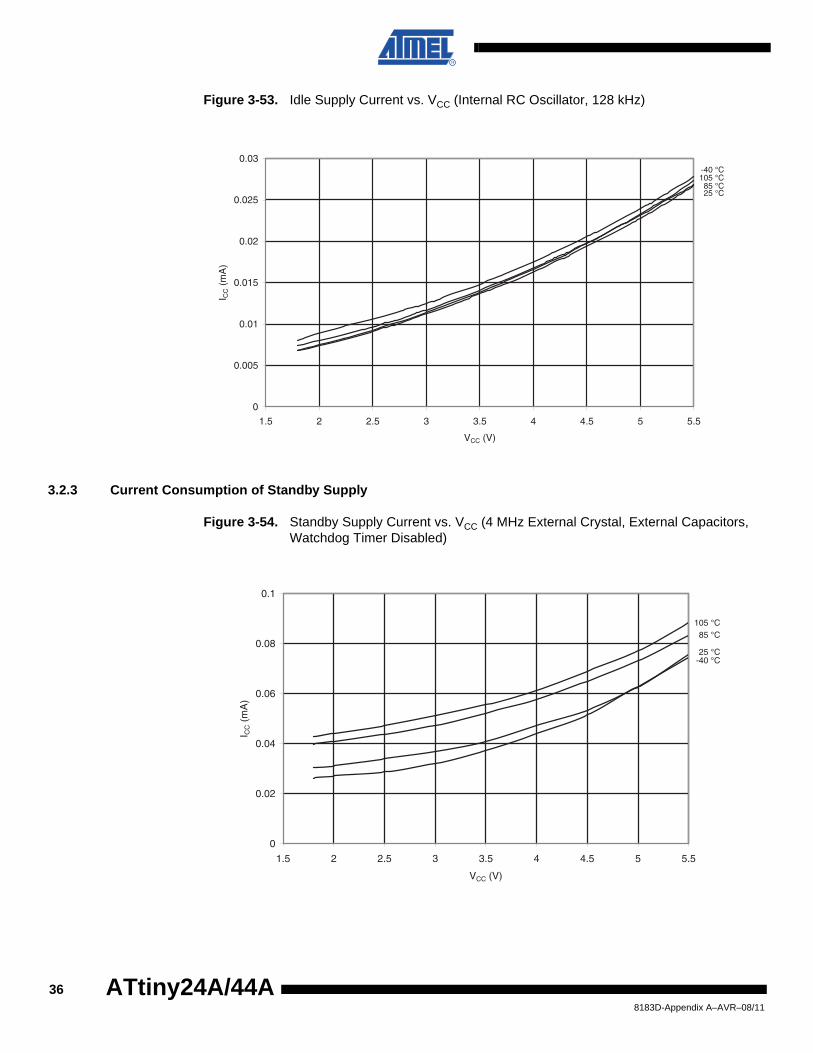
Figure 3-53. Idle Supply Current vs. VCC (Internal RC Oscillator, 128 kHz)
3.2.3 Current Consumption of Standby Supply
Figure 3-54. Standby Supply Current vs. VCC (4 MHz External Crystal, External Capacitors, Watchdog Timer Disabled)
105 °C85 °C25 °C
-40 °C
0
0.005
0.01
0.015
0.02
0.025
0.03
1.5 2 2.5 3 3.5 4 4.5 5 5.5
VCC (V)
I CC (
mA
)
105 °C85 °C
25 °C-40 °C
0
0.02
0.04
0.06
0.08
0.1
1.5 2 2.5 3 3.5 4 4.5 5 5.5
VCC (V)
I CC (
mA
)
368183D-Appendix A–AVR–08/11
ATtiny24A/44A
ATtiny24A/44A
3.2.4 Current Consumption in Power-down Supply Mode
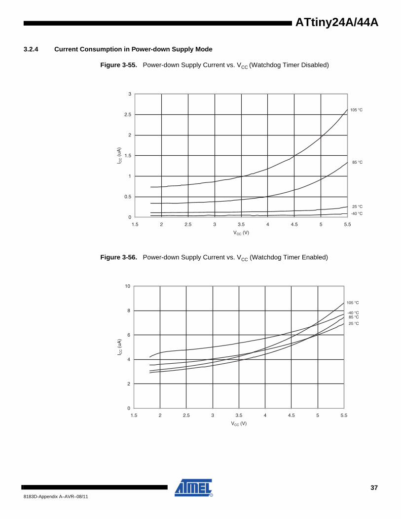
Figure 3-55. Power-down Supply Current vs. VCC (Watchdog Timer Disabled)
Figure 3-56. Power-down Supply Current vs. VCC (Watchdog Timer Enabled)
105 °C
85 °C
25 °C
-40 °C0
0.5
1
1.5
2
2.5
3
1.5 2 2.5 3 3.5 4 4.5 5 5.5
VCC (V)
I CC (
uA)
105 °C
85 °C
25 °C
-40 °C
0
2
4
6
8
10
1.5 2 2.5 3 3.5 4 4.5 5 5.5
VCC (V)
I CC (
uA)
378183D-Appendix A–AVR–08/11
3.2.5 Current Consumption of Peripheral Units
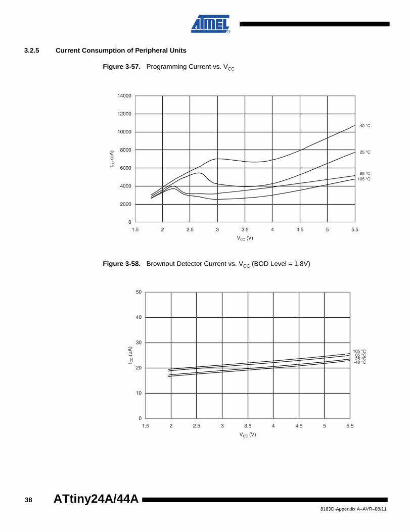
Figure 3-57. Programming Current vs. VCC
Figure 3-58. Brownout Detector Current vs. VCC (BOD Level = 1.8V)
105 °C85 °C
25 °C
-40 °C
0
2000
4000
6000
8000
10000
12000
14000
1.5 2 2.5 3 3.5 4 4.5 5 5.5
VCC (V)
I CC (
uA)
105 °C85 °C25 °C
-40 °C
0
10
20
30
40
50
1.5 2 2.5 3 3.5 4 4.5 5 5.5
VCC (V)
I CC (
uA)
388183D-Appendix A–AVR–08/11
ATtiny24A/44A
ATtiny24A/44A
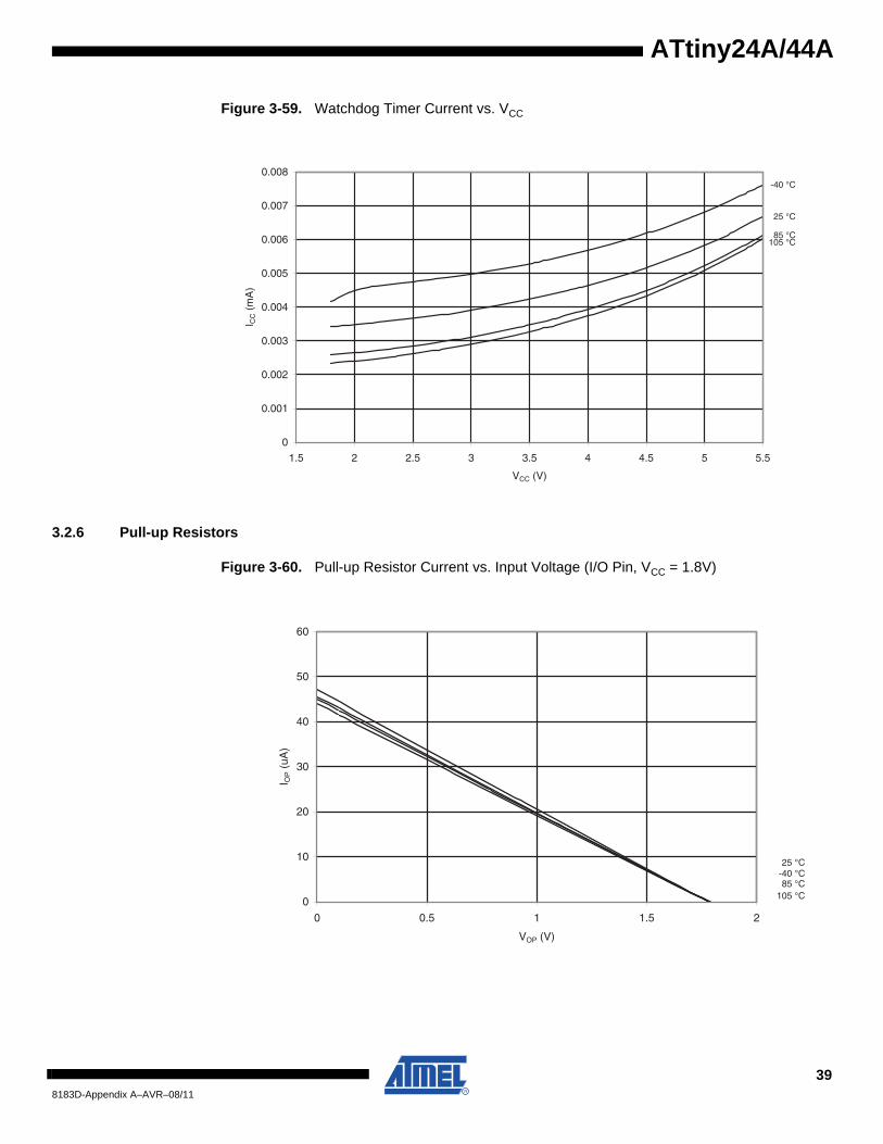
Figure 3-59. Watchdog Timer Current vs. VCC
3.2.6 Pull-up Resistors
Figure 3-60. Pull-up Resistor Current vs. Input Voltage (I/O Pin, VCC = 1.8V)
105 °C85 °C
25 °C
-40 °C
0
0.001
0.002
0.003
0.004
0.005
0.006
0.007
0.008
1.5 2 2.5 3 3.5 4 4.5 5 5.5
VCC (V)
I CC (
mA
)
0
10
20
30
40
50
60
0 0.5 1 1.5 2
VOP (V)
I OP (
uA)
105 °C85 °C
25 °C-40 °C
398183D-Appendix A–AVR–08/11
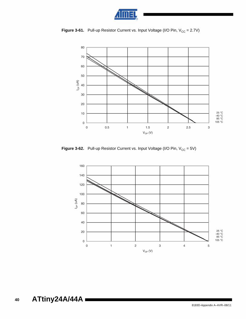
Figure 3-61. Pull-up Resistor Current vs. Input Voltage (I/O Pin, VCC = 2.7V)
Figure 3-62. Pull-up Resistor Current vs. Input Voltage (I/O Pin, VCC = 5V)
105 °C85 °C
25 °C-40 °C
0
10
20
30
40
50
60
70
80
0 0.5 1 1.5 2 2.5 3
VOP (V)
I OP (
uA)
105 °C85 °C
25 °C-40 °C
0
20
40
60
80
100
120
140
160
0 1 2 3 4 5
VOP (V)
I OP (
uA)
408183D-Appendix A–AVR–08/11
ATtiny24A/44A
ATtiny24A/44A
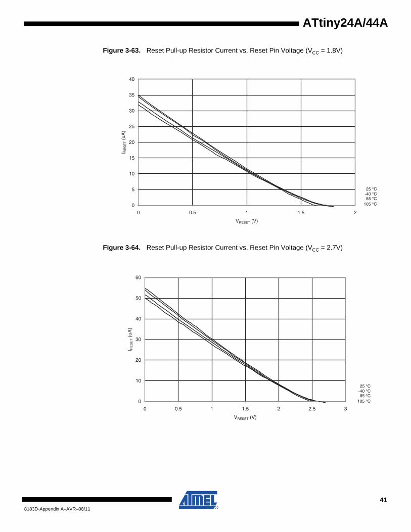
Figure 3-63. Reset Pull-up Resistor Current vs. Reset Pin Voltage (VCC = 1.8V)
Figure 3-64. Reset Pull-up Resistor Current vs. Reset Pin Voltage (VCC = 2.7V)
0
5
10
15
20
25
30
35
40
0 0.5 1 1.5 2
VRESET (V)
I RE
SE
T (
uA)
105 °C85 °C
25 °C-40 °C
105 °C85 °C
25 °C-40 °C
0
10
20
30
40
50
60
0 0.5 1 1.5 2 2.5 3
VRESET (V)
I RE
SE
T (
uA)
418183D-Appendix A–AVR–08/11
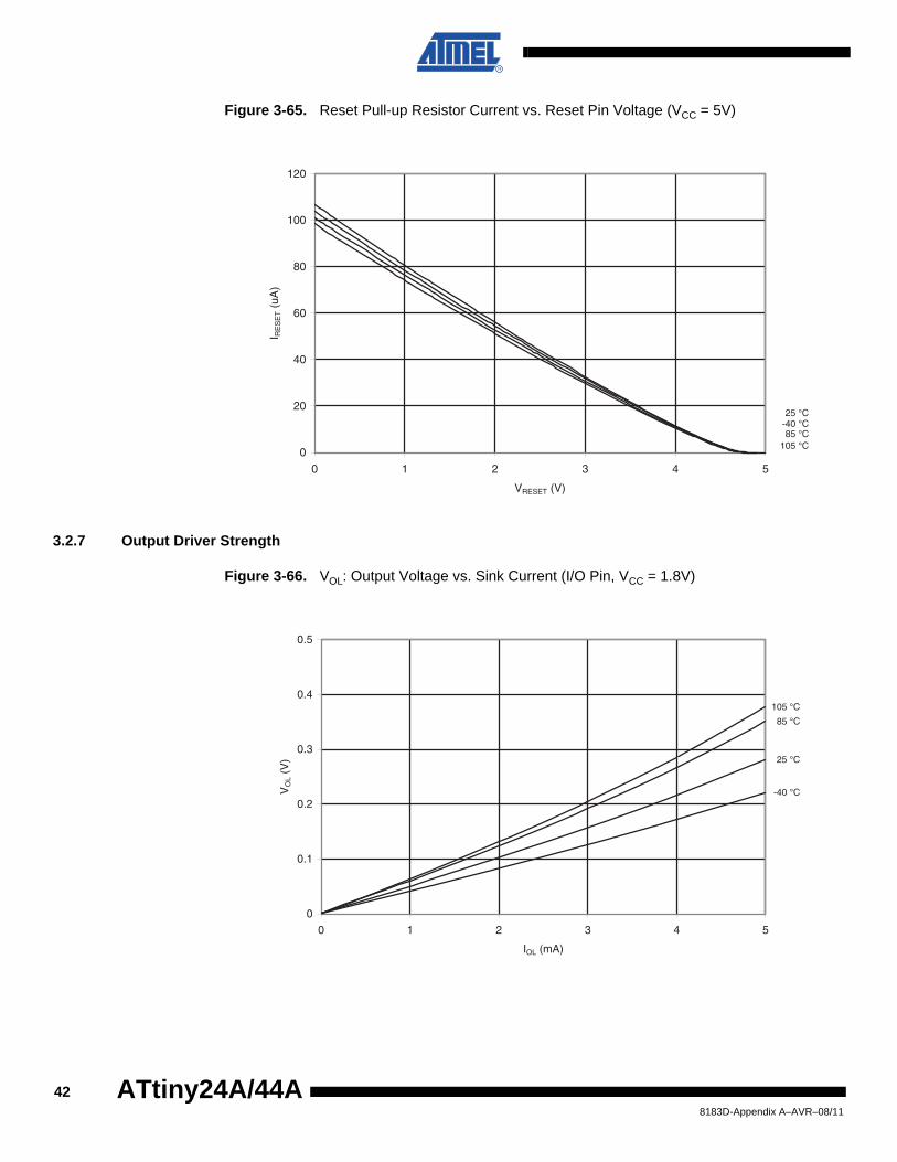
Figure 3-65. Reset Pull-up Resistor Current vs. Reset Pin Voltage (VCC = 5V)
3.2.7 Output Driver Strength
Figure 3-66. VOL: Output Voltage vs. Sink Current (I/O Pin, VCC = 1.8V)
105 °C85 °C
25 °C-40 °C
0
20
40
60
80
100
120
0 1 2 3 4 5
VRESET (V)
I RE
SE
T (
uA)
105 °C
85 °C
25 °C
-40 °C
0
0.1
0.2
0.3
0.4
0.5
0 1 2 3 4 5
IOL (mA)
VO
L (V
)
428183D-Appendix A–AVR–08/11
ATtiny24A/44A
ATtiny24A/44A
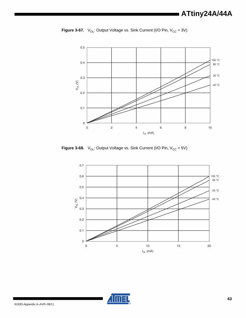
Figure 3-67. VOL: Output Voltage vs. Sink Current (I/O Pin, VCC = 3V)
Figure 3-68. VOL: Output Voltage vs. Sink Current (I/O Pin, VCC = 5V)
105 °C
85 °C
25 °C
-40 °C
0
0.1
0.2
0.3
0.4
0.5
0 2 4 6 8 10
IOL (mA)
VO
L (V
)
105 °C
85 °C
25 °C
-40 °C
0
0.1
0.2
0.3
0.4
0.5
0.6
0.7
0 5 10 15 20
IOL (mA)
VO
L (V
)
438183D-Appendix A–AVR–08/11
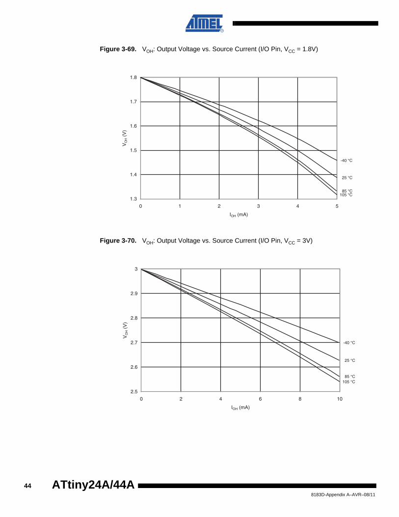
Figure 3-69. VOH: Output Voltage vs. Source Current (I/O Pin, VCC = 1.8V)
Figure 3-70. VOH: Output Voltage vs. Source Current (I/O Pin, VCC = 3V)
105 °C85 °C
25 °C
-40 °C
1.3
1.4
1.5
1.6
1.7
1.8
0 1 2 3 4 5
IOH (mA)
VO
H (
V)
105 °C85 °C
25 °C
-40 °C
2.5
2.6
2.7
2.8
2.9
3
0 2 4 6 8 10
IOH (mA)
VO
H (
V)
448183D-Appendix A–AVR–08/11
ATtiny24A/44A
ATtiny24A/44A
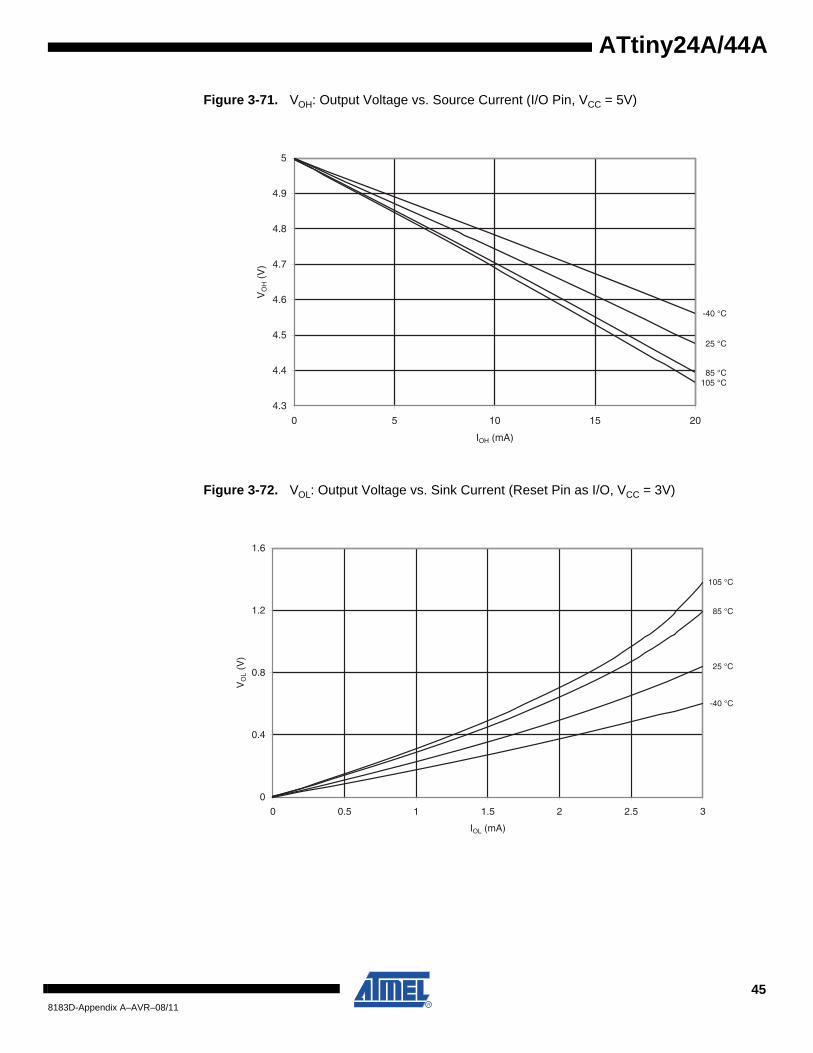
Figure 3-71. VOH: Output Voltage vs. Source Current (I/O Pin, VCC = 5V)
Figure 3-72. VOL: Output Voltage vs. Sink Current (Reset Pin as I/O, VCC = 3V)
105 °C85 °C
25 °C
-40 °C
4.3
4.4
4.5
4.6
4.7
4.8
4.9
5
0 5 10 15 20
IOH (mA)
VO
H (
V)
105 °C
85 °C
25 °C
-40 °C
0
0.4
0.8
1.2
1.6
0 0.5 1 1.5 2 2.5 3
IOL (mA)
VO
L (V
)
458183D-Appendix A–AVR–08/11
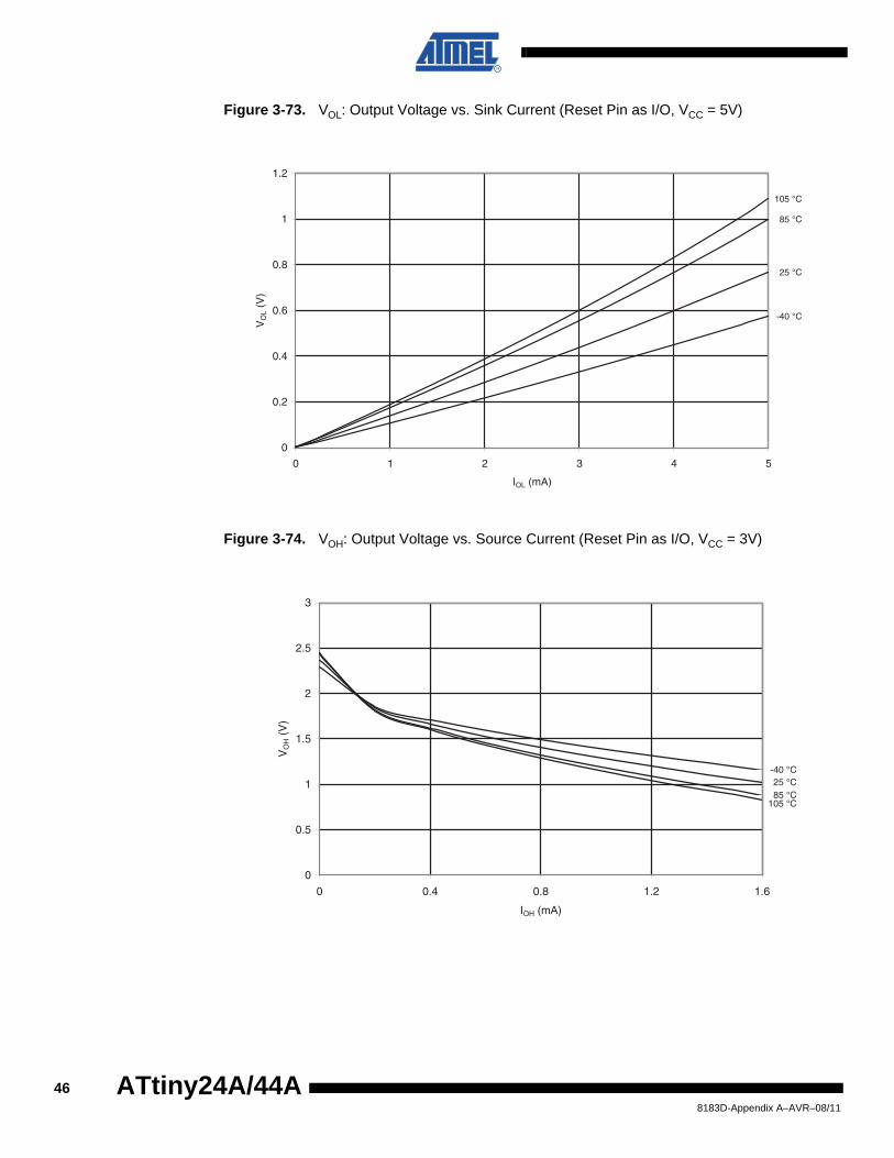
Figure 3-73. VOL: Output Voltage vs. Sink Current (Reset Pin as I/O, VCC = 5V)
Figure 3-74. VOH: Output Voltage vs. Source Current (Reset Pin as I/O, VCC = 3V)
105 °C
85 °C
25 °C
-40 °C
0
0.2
0.4
0.6
0.8
1
1.2
0 1 2 3 4 5
IOL (mA)
VO
L (V
)
105 °C85 °C25 °C
-40 °C
0
0.5
1
1.5
2
2.5
3
0 0.4 0.8 1.2 1.6
IOH (mA)
VO
H (
V)
468183D-Appendix A–AVR–08/11
ATtiny24A/44A
ATtiny24A/44A
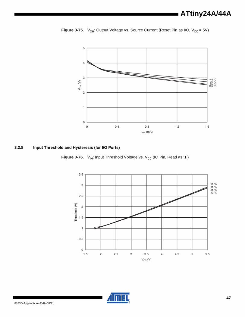
Figure 3-75. VOH: Output Voltage vs. Source Current (Reset Pin as I/O, VCC = 5V)
3.2.8 Input Threshold and Hysteresis (for I/O Ports)
Figure 3-76. VIH: Input Threshold Voltage vs. VCC (IO Pin, Read as ‘1’)
105 °C85 °C25 °C
-40 °C
0
1
2
3
4
5
0 0.4 0.8 1.2 1.6
IOH (mA)
VO
H (
V)
105 °C85 °C25 °C
-40 °C
0
0.5
1
1.5
2
2.5
3
3.5
1.5 2 2.5 3 3.5 4 4.5 5 5.5
VCC (V)
Thr
esho
ld (
V)
478183D-Appendix A–AVR–08/11
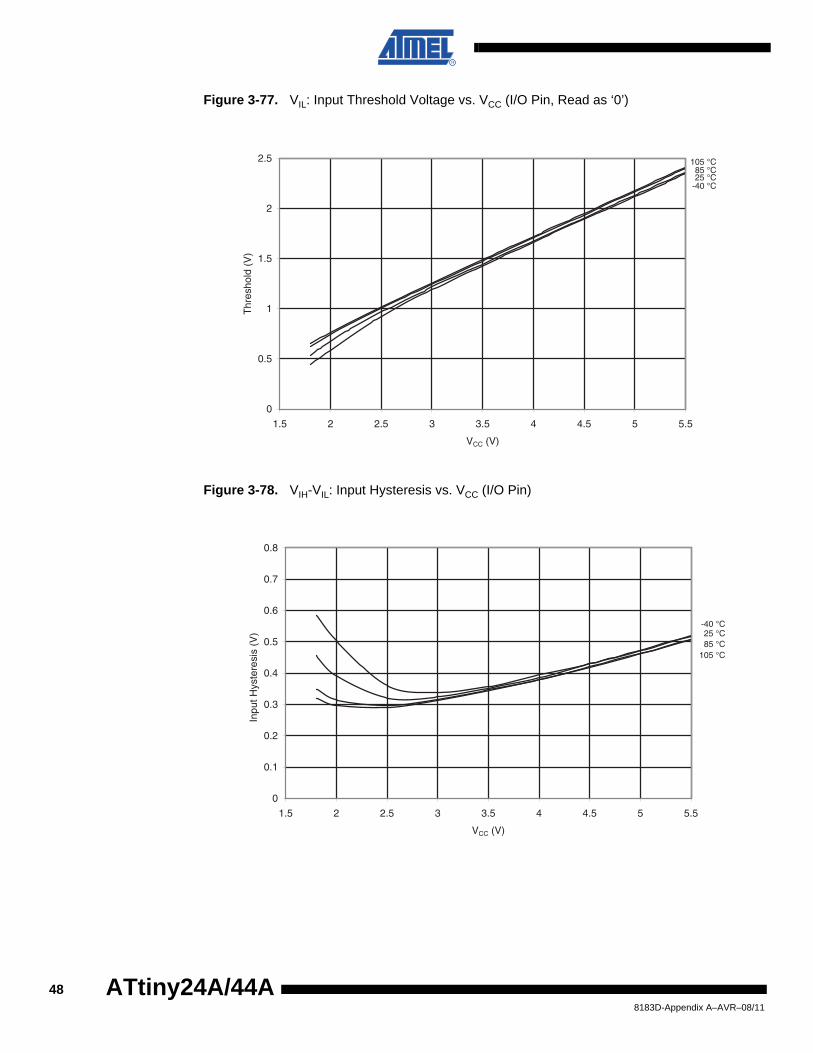
Figure 3-77. VIL: Input Threshold Voltage vs. VCC (I/O Pin, Read as ‘0’)
Figure 3-78. VIH-VIL: Input Hysteresis vs. VCC (I/O Pin)
105 °C85 °C25 °C
-40 °C
0
0.5
1
1.5
2
2.5
1.5 2 2.5 3 3.5 4 4.5 5 5.5
VCC (V)
Thr
esho
ld (
V)
105 °C85 °C25 °C
-40 °C
0
0.1
0.2
0.3
0.4
0.5
0.6
0.7
0.8
1.5 2 2.5 3 3.5 4 4.5 5 5.5
VCC (V)
Inpu
t Hys
tere
sis
(V)
488183D-Appendix A–AVR–08/11
ATtiny24A/44A
ATtiny24A/44A
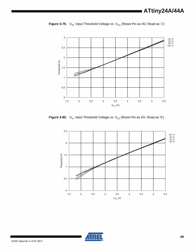
Figure 3-79. VIH: Input Threshold Voltage vs. VCC (Reset Pin as I/O, Read as ‘1’)
Figure 3-80. VIL: Input Threshold Voltage vs. VCC (Reset Pin as I/O, Read as ‘0’)
105 °C85 °C25 °C
-40 °C
0
0.5
1
1.5
2
2.5
3
1.5 2 2.5 3 3.5 4 4.5 5 5.5
VCC (V)
Thr
esho
ld (
V)
105 °C85 °C25 °C
-40 °C
0
0.5
1
1.5
2
2.5
1.5 2 2.5 3 3.5 4 4.5 5 5.5
VCC (V)
Thr
esho
ld (
V)
498183D-Appendix A–AVR–08/11
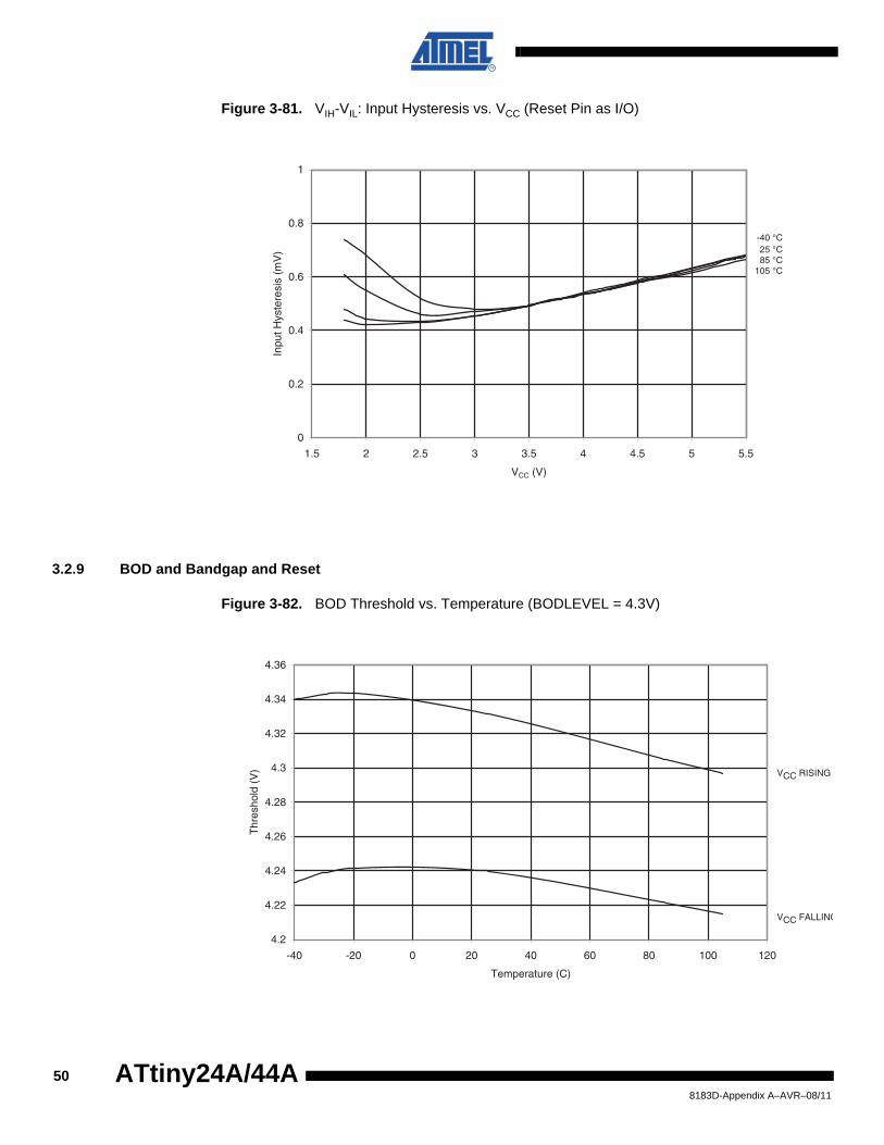
Figure 3-81. VIH-VIL: Input Hysteresis vs. VCC (Reset Pin as I/O)
3.2.9 BOD and Bandgap and Reset
Figure 3-82. BOD Threshold vs. Temperature (BODLEVEL = 4.3V)
105 °C85 °C25 °C
-40 °C
0
0.2
0.4
0.6
0.8
1
1.5 2 2.5 3 3.5 4 4.5 5 5.5
VCC (V)
Inpu
t Hys
tere
sis
(mV
)
4.2
4.22
4.24
4.26
4.28
4.3
4.32
4.34
4.36
-40 -20 0 20 40 60 80 100 120
Temperature (C)
Thr
esho
ld (
V) VCC RISING
VCC FALLING
508183D-Appendix A–AVR–08/11
ATtiny24A/44A
ATtiny24A/44A
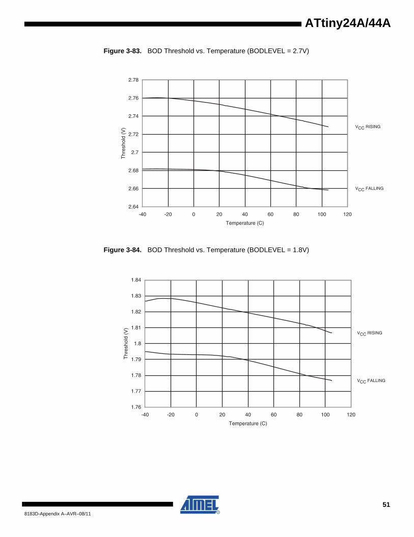
Figure 3-83. BOD Threshold vs. Temperature (BODLEVEL = 2.7V)
Figure 3-84. BOD Threshold vs. Temperature (BODLEVEL = 1.8V)
2.64
2.66
2.68
2.7
2.72
2.74
2.76
2.78
-40 -20 0 20 40 60 80 100 120
Temperature (C)
Thr
esho
ld (
V) VCC RISING
VCC FALLING
VCC RISING
VCC FALLING
1.76
1.77
1.78
1.79
1.8
1.81
1.82
1.83
1.84
-40 -20 0 20 40 60 80 100 120
Temperature (C)
Thr
esho
ld (
V)
518183D-Appendix A–AVR–08/11
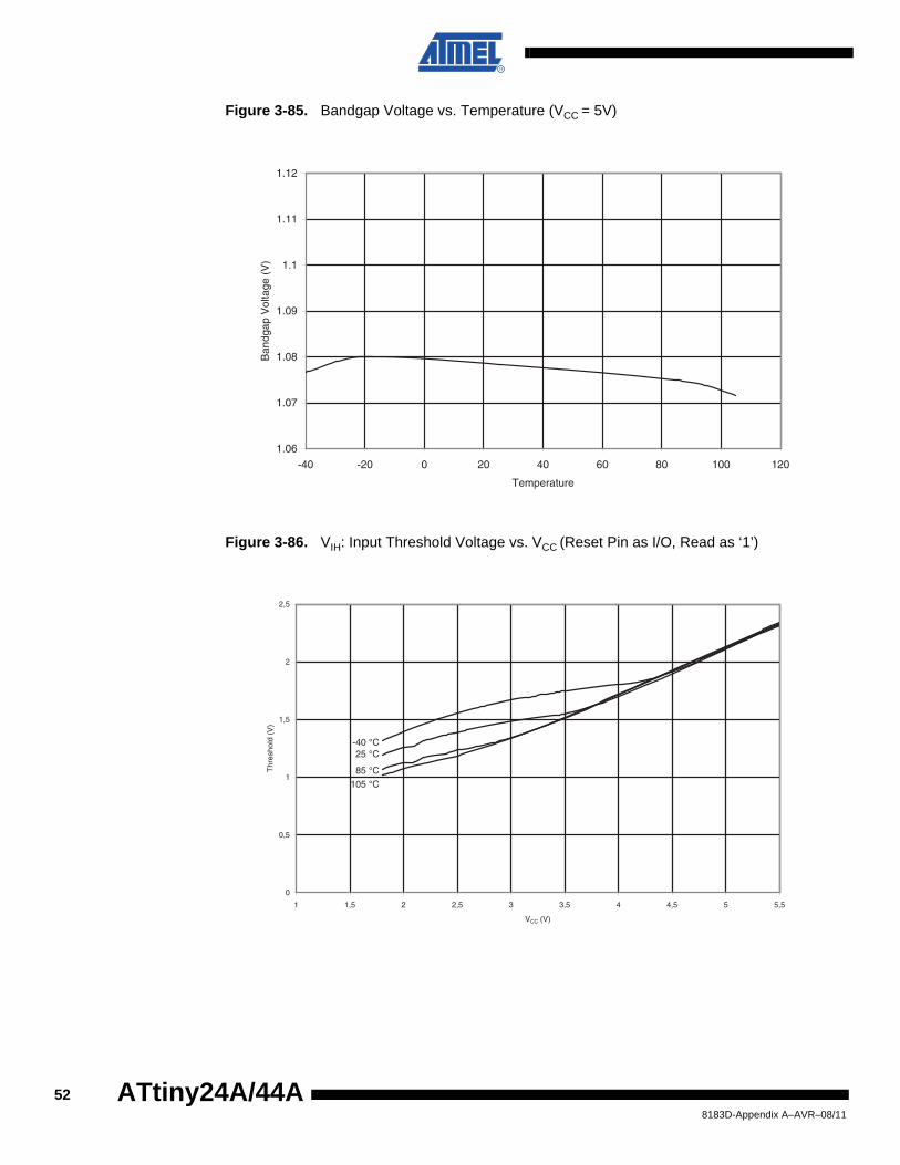
Figure 3-85. Bandgap Voltage vs. Temperature (VCC = 5V)
Figure 3-86. VIH: Input Threshold Voltage vs. VCC (Reset Pin as I/O, Read as ‘1’)
1.06
1.07
1.08
1.09
1.1
1.11
1.12
-40 -20 0 20 40 60 80 100 120
Temperature
Ban
dgap
Vol
tage
(V
)
105 °C
85 °C
25 °C-40 °C
0
0,5
1
1,5
2
2,5
1 1,5 2 2,5 3 3,5 4 4,5 5 5,5
VCC (V)
Thr
esho
ld (
V)
528183D-Appendix A–AVR–08/11
ATtiny24A/44A
ATtiny24A/44A
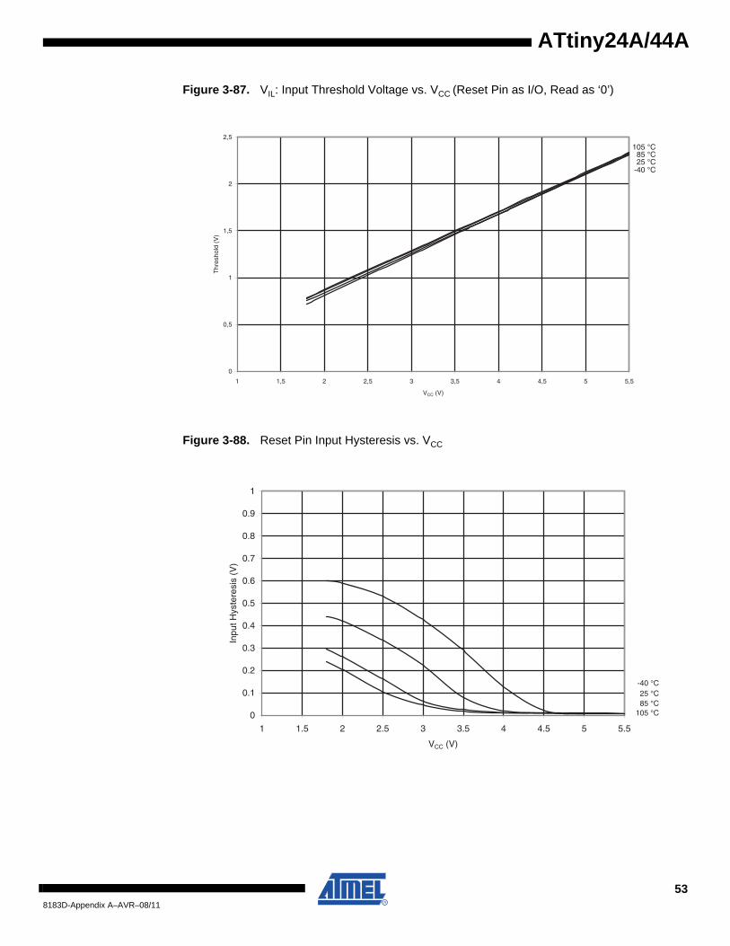
Figure 3-87. VIL: Input Threshold Voltage vs. VCC (Reset Pin as I/O, Read as ‘0’)
Figure 3-88. Reset Pin Input Hysteresis vs. VCC
105 °C85 °C25 °C
-40 °C
0
0,5
1
1,5
2
2,5
1 1,5 2 2,5 3 3,5 4 4,5 5 5,5
VCC (V)
Thr
esho
ld (
V)
105 °C85 °C25 °C
-40 °C
0
0.1
0.2
0.3
0.4
0.5
0.6
0.7
0.8
0.9
1
1 1.5 2 2.5 3 3.5 4 4.5 5 5.5
VCC (V)
Inpu
t Hys
tere
sis
(V)
538183D-Appendix A–AVR–08/11
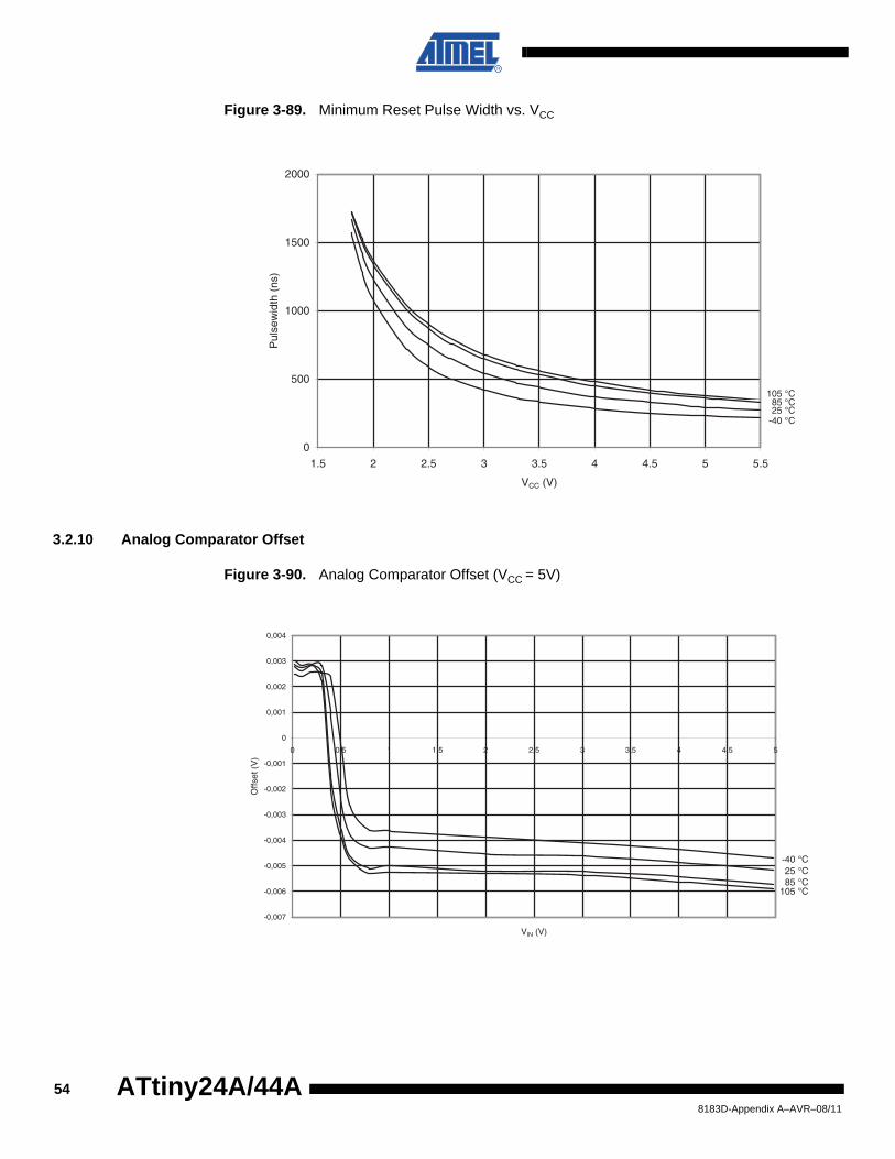
Figure 3-89. Minimum Reset Pulse Width vs. VCC
3.2.10 Analog Comparator Offset
Figure 3-90. Analog Comparator Offset (VCC = 5V)
105 °C85 °C25 °C
-40 °C
0
500
1000
1500
2000
1.5 2 2.5 3 3.5 4 4.5 5 5.5
VCC (V)
Pul
sew
idth
(ns
)
105 °C85 °C25 °C
-40 °C
-0,007
-0,006
-0,005
-0,004
-0,003
-0,002
-0,001
0
0,001
0,002
0,003
0,004
0 0,5 1 1,5 2 2,5 3 3,5 4 4,5 5
VIN (V)
Offs
et (
V)
548183D-Appendix A–AVR–08/11
ATtiny24A/44A
ATtiny24A/44A
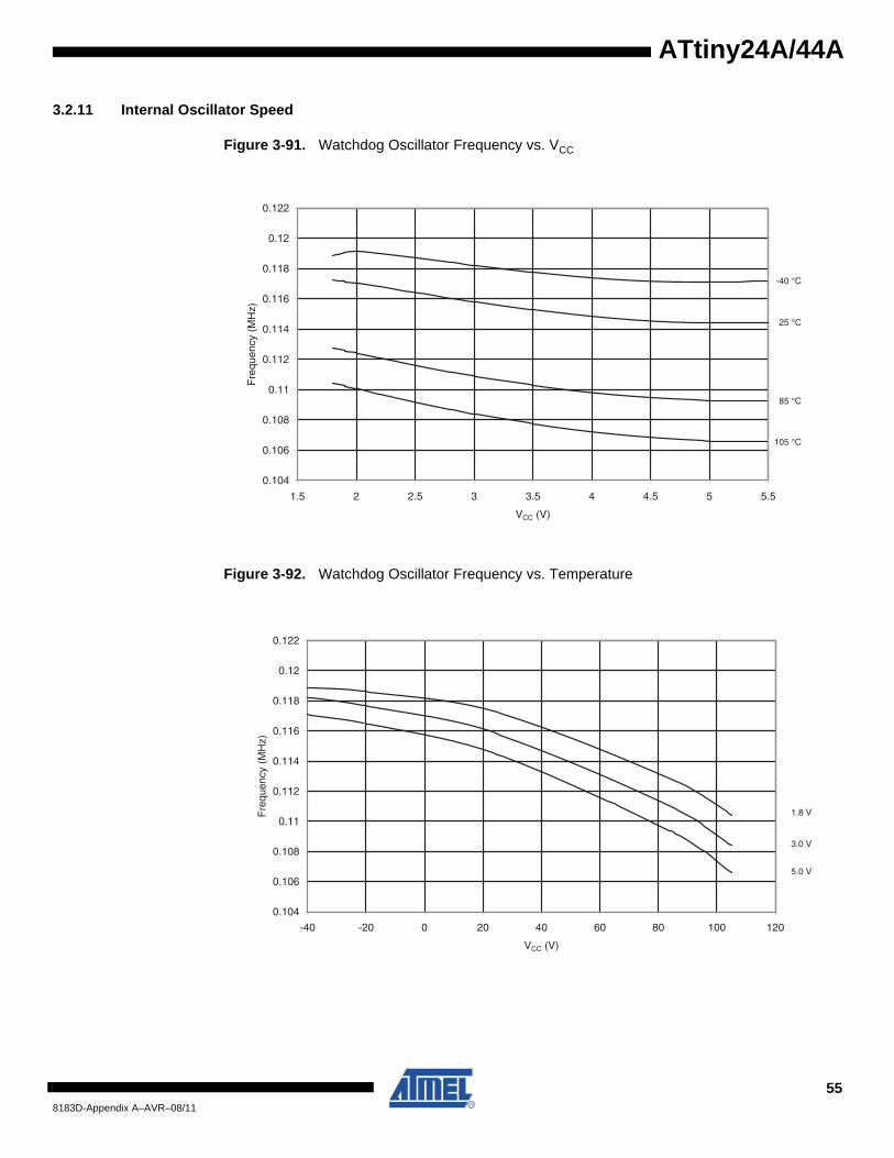
3.2.11 Internal Oscillator Speed
Figure 3-91. Watchdog Oscillator Frequency vs. VCC
Figure 3-92. Watchdog Oscillator Frequency vs. Temperature
105 °C
85 °C
25 °C
-40 °C
0.104
0.106
0.108
0.11
0.112
0.114
0.116
0.118
0.12
0.122
1.5 2 2.5 3 3.5 4 4.5 5 5.5
VCC (V)
Fre
quen
cy (
MH
z)
1.8 V
3.0 V
5.0 V
0.104
0.106
0.108
0.11
0.112
0.114
0.116
0.118
0.12
0.122
-40 -20 0 20 40 60 80 100 120
VCC (V)
Fre
quen
cy (
MH
z)
558183D-Appendix A–AVR–08/11
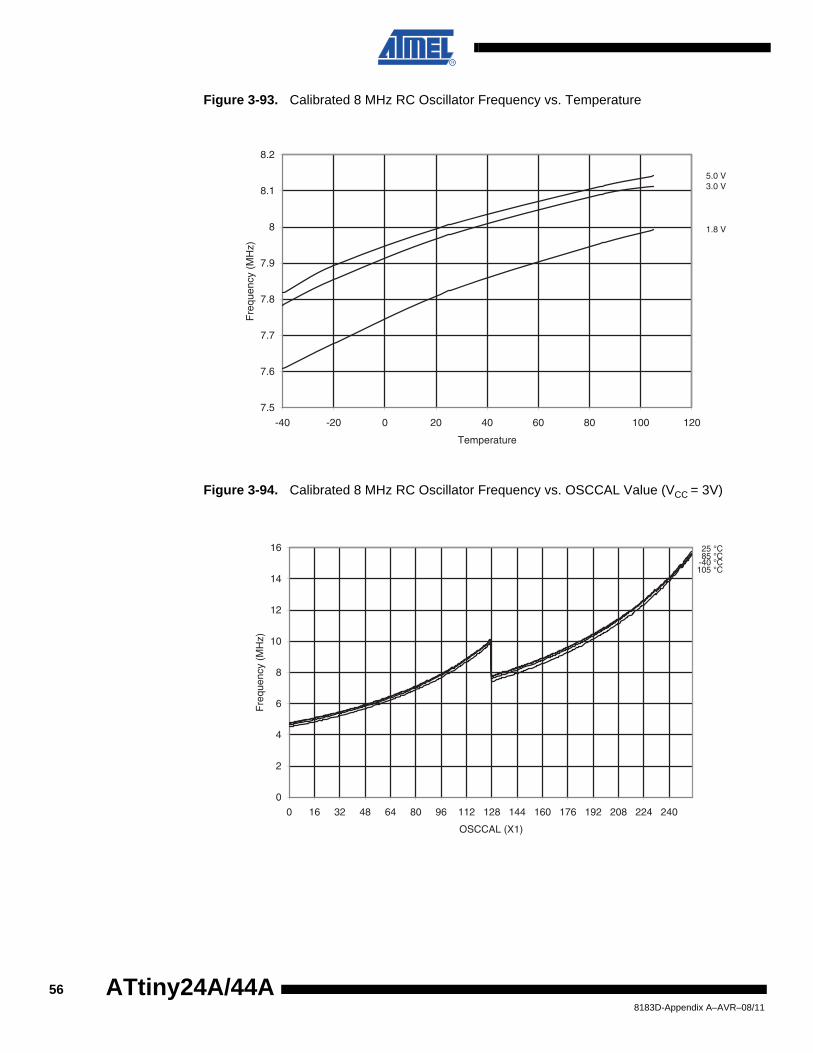
Figure 3-93. Calibrated 8 MHz RC Oscillator Frequency vs. Temperature
Figure 3-94. Calibrated 8 MHz RC Oscillator Frequency vs. OSCCAL Value (VCC = 3V)
5.0 V3.0 V
1.8 V
7.5
7.6
7.7
7.8
7.9
8
8.1
8.2
-40 -20 0 20 40 60 80 100 120
Temperature
Fre
quen
cy (
MH
z)
105 °C
85 °C25 °C
-40 °C
0
2
4
6
8
10
12
14
16
0 16 32 48 64 80 96 112 128 144 160 176 192 208 224 240
OSCCAL (X1)
Fre
quen
cy (
MH
z)
568183D-Appendix A–AVR–08/11
ATtiny24A/44A
ATtiny24A/44A
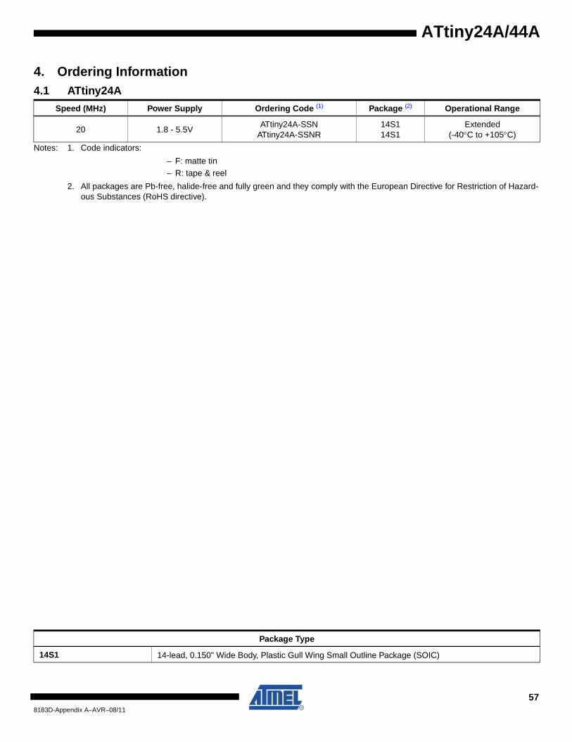
4. Ordering Information
Notes: 1. Code indicators:
– F: matte tin– R: tape & reel
2. All packages are Pb-free, halide-free and fully green and they comply with the European Directive for Restriction of Hazard-ous Substances (RoHS directive).
4.1 ATtiny24A
Speed (MHz) Power Supply Ordering Code (1) Package (2) Operational Range
20 1.8 - 5.5VATtiny24A-SSN
ATtiny24A-SSNR14S114S1
Extended(-40°C to +105°C)
Package Type
14S1 14-lead, 0.150" Wide Body, Plastic Gull Wing Small Outline Package (SOIC)
578183D-Appendix A–AVR–08/11
Notes: 1. Code indicators:
– F: matte tin
– R: tape & reel
2. All packages are Pb-free, halide-free and fully green and they comply with the European Directive for Restriction of Hazard-ous Substances (RoHS directive).
4.2 ATtiny44A
Speed (MHz) Power Supply Ordering Code (1) Package (2) Operational Range
20 1.8 - 5.5VATtiny44A-SSNATtiny44A-SSNR
14S114S1
Extended(-40°C to +105°C)
Package Type
14S1 14-lead, 0.150" Wide Body, Plastic Gull Wing Small Outline Package (SOIC)
588183D-Appendix A–AVR–08/11
ATtiny24A/44A
ATtiny24A/44A
5. Revision History
Revision No. History
8183A–Appendix A–AVR–12/10 Initial revision
8183D–Appendix A–AVR–08/11 Added ordering codes for tape&reel
598183D-Appendix A–AVR–08/11
8183D-Appendix A–AVR–08/11
Headquarters International
Atmel Corporation2325 Orchard ParkwaySan Jose, CA 95131USATel: (+1)(408) 441-0311Fax: (+1)(408) 487-2600
Atmel Asia LimitedUnit 01-5 & 16, 19FBEA Tower, Millennium City 5418 Kwun Tong RoadKwun Tong, KowloonHONG KONGTel: (+852) 2245-6100Fax: (+852) 2722-1369
Atmel Munich GmbHBusiness CampusParkring 4D-85748 Garching b. MunichGERMANYTel: (+49) 89-31970-0 Fax: (+49) 89-3194621
Atmel Japan9F, Tonetsu Shinkawa Bldg.1-24-8 ShinkawaChuo-ku, Tokyo 104-0033JAPANTel: (+81)(3) 3523-3551Fax: (+81)(3) 3523-7581
Product Contact
Web Sitewww.atmel.com
Technical [email protected]
Sales Contactwww.atmel.com/contacts
Literature Requestswww.atmel.com/literature
Disclaimer: The information in this document is provided in connection with Atmel products. No license, express or implied, by estoppel or otherwise, to anyintellectual property right is granted by this document or in connection with the sale of Atmel products. EXCEPT AS SET FORTH IN ATMEL’S TERMS AND CONDI-TIONS OF SALE LOCATED ON ATMEL’S WEB SITE, ATMEL ASSUMES NO LIABILITY WHATSOEVER AND DISCLAIMS ANY EXPRESS, IMPLIED OR STATUTORYWARRANTY RELATING TO ITS PRODUCTS INCLUDING, BUT NOT LIMITED TO, THE IMPLIED WARRANTY OF MERCHANTABILITY, FITNESS FOR A PARTICULARPURPOSE, OR NON-INFRINGEMENT. IN NO EVENT SHALL ATMEL BE LIABLE FOR ANY DIRECT, INDIRECT, CONSEQUENTIAL, PUNITIVE, SPECIAL OR INCIDEN-TAL DAMAGES (INCLUDING, WITHOUT LIMITATION, DAMAGES FOR LOSS OF PROFITS, BUSINESS INTERRUPTION, OR LOSS OF INFORMATION) ARISING OUT OFTHE USE OR INABILITY TO USE THIS DOCUMENT, EVEN IF ATMEL HAS BEEN ADVISED OF THE POSSIBILITY OF SUCH DAMAGES. Atmel makes norepresentations or warranties with respect to the accuracy or completeness of the contents of this document and reserves the right to make changes to specificationsand product descriptions at any time without notice. Atmel does not make any commitment to update the information contained herein. Unless specifically providedotherwise, Atmel products are not suitable for, and shall not be used in, automotive applications. Atmel’s products are not intended, authorized, or warranted for useas components in applications intended to support or sustain life.
© 2011 Atmel Corporation. All rights reserved.
Atmel®, logo and combinations thereof, and others are registered trademarks or trademarks of Atmel Corporation or its subsidiaries. Other termsand product names may be trademarks of others.


![ATtiny24A/44A Datasheet Summary - Farnell element14 · 2012. 5. 18. · 0x27 (0x47) DWDR DWDR[7:0] Page 151 0x26 (0x46) CLKPR CLKPCE – – – CLKPS3 CLKPS2 CLKPS1 CLKPS0 Page 30](https://img.pdfslide.us/doc/110x75/60be801c3ef8237243479d2c/attiny24a44a-datasheet-summary-farnell-element14-2012-5-18-0x27-0x47-dwdr.jpg)


![ATtiny24A, ATtiny44A, ATtiny84Aww1.microchip.com/downloads/en/DeviceDoc/Atmel-8183-AVR...ATtiny24A/44A/84A [DATASHEET APPENDIX B] 5 8183H–AVR–10/2013 2.3 Speed 2.3.1 ATtiny24A](https://img.pdfslide.us/doc/110x75/60ae66b91bc26245a80fdd7c/attiny24a-attiny44a-attiny24a44a84a-datasheet-appendix-b-5-8183haavra102013.jpg)
![ATtiny24A, ATtiny44A, ATtiny84A · 2018. 8. 17. · ATtiny24A/44A/84A [DATASHEET APPENDIX B] 5 8183H–AVR–10/2013 2.3 Speed 2.3.1 ATtiny24A and ATtiny44A The maximum operating](https://img.pdfslide.us/doc/110x75/606ee5f536c3b81d810e4d6e/attiny24a-attiny44a-attiny84a-2018-8-17-attiny24a44a84a-datasheet-appendix.jpg)