Embed Size (px)
Citation preview

Slide 14
Appendix 0: Main Body SupportReferences and Further Investigation• J. Moore, M. McLean, “FPGA Single Chip Cryptographic Solution”, Proceedings of the 2006
SDR Technical Conference and Product Exhibition http://www.sdrforum.org/pages/sdr06/sdr06_papers/1.3/1.3-04.pdf
– More on SCC: http://www.xilinx.com/products/silicon_solutions/market_specific_devices/aero_def/capabilities/crypto.htm
• C. Carmicael, J. George, G. Miller, G. Swift, G. Allen, CW Tseng, “Static Upset Characteristics of the 90nm Virtex-4QV FPGAs”, Proceedings of the 2008 NSREC Technical Conference
– More on Virtex-4QV and mitigation http://www.xilinx.com/products/silicon_solutions/aero_def/4qv_promo.htm
• XAPP988 Correcting SEUs in Virtex-4 Platform FPGA Configuration Memory• XAPP989 Correcting SEUs with a Self-Hosting Configuration Management Core • XAPP1004 Single-Event Upset Mitigation Design Flow for Xilinx FPGA PowerPC Systems• XAPP962 : Single-Event Upset Mitigation for Xilinx FPGA Block Memories• XAPP1051 : Single Event Upset Mitigation Design Flow for Xilinx FPGA MicroBlaze
Systems

Slide 15
MAPLD Applications Section -Secure SDR in Space Abstract
Software Defined Radio (SDR) has now become a common practice. What was the subject of debate and dreams a decade ago has now become reality in as small a form factor as hand-held radios for soldiers and in micro-satellites. Many of these communications transmit sensitive information for government, military or financial applications. Thus, they require the data to be encrypted. Of course, SDR in space is an extra challenge because it requires high-performance computing in a radiation-intensive environment. In this session, we discuss the architecture of a card which can provide secure SDR in space. Then, we look into a software flow for how this application can be implemented with modern high-performance, radiation-tolerant and reprogrammable FPGAs. This flow combines a unique methodology for secure communications which has multiple independent levels of security and isolation of the channels along with intellectual property made redundant by using a software tool that automates the process of triple modular redundancy. This discussion will consider the large variety of waveforms and cryptographic algorithms which can be performed by an FPGA, even looking at how one might change waveforms through partial reconfiguration with the satellite while in service. Finally, we will discuss some good design practices for intellectual property and the overall board subsystem in space.

Slide 16
Software Flows: Tool Elements
• Basic Hardware Flow– Block-level generation– Design / Code Entry – Simulation– Synthesis / physical
synthesis– Simulation– Place and route– Timing closure/back
annotation– Bitstream Generation
• Other useful tools– DSP System & Simulation
• Accelchip (DSP synthesis)• Simulink / System Generator
– MPU SW Development• Platform Studio• Embedded Development Kit
– PlanAhead (Floorplanner)– Chipscope (Debug / Probe)

Slide 17
XPS / TMR Tool Design Flow
System DesignXPS
Netlist Creation
TMR Tool
NGDBuild
MAP
PAR
BitGen / BitInit
Design EntryEDK/ISE
XTMR ConversionTMR Tool
ImplementationISE
.ngc
.bmm
.elf
.edf
(Manual edit).ucf
.ngo
BRAM Macro Replacement
PPC Converge
“C” Compiler

Slide 18
Mitigation Considerations• Methods are application & orbit dependant
– SWAP constraints– Processing performance– Reliability requirements– Design schedule– Type of data and peripherals– Latency constraints
• Weigh factors before implementing an approach• Designs often use multiple mitigation methods Pr
oces
sing
Perfo
rman
cepe
r unit
of S
WAP
Effort
Proc
essin
gPe
rform
ance
per u
nit of
SW
AP
Reliability
V4-RCC Board Supports Wide Range of SEE Mitigation Approaches
Courtesy of SEAKR Engineering

Slide 19
Virtex-4QV Orbital Rates
Configuration Memory Cells
Upsets/Device-DayTypical Solar Conditions
XQR4VSX55 0.76 7.43 5.12 20.0 4.20
XQR4VFX60 0.80 7.79 5.36 20.9 4.40
XQR4VFX140 - - - - -
XQR4VLX200 2.15 21.0 14.5 56.5 11.9
Functional Interrupts (All Virtex-4)
Upsets/Device-DayTypical Solar Conditions
0°65.0°98.7°22.0°51.6°
36,0001,200833800400
GEOCONST.POLARLEOLEOOrbit
Altitude (km)
Inclination
10313.35336412All SEFIs (Combined)
Device-Years Between Event
4.87E-066.47E-051.57E-052.41E-051.57E-06GSIG
9.46E-066.71E-051.69E-052.45E-052.25E-06SMAP+FAR
1.21E-057.36E-051.85E-052.73E-052.83E-06POR
Notes: 1) Unmitigated Device Performance2) Reference: Gary Swift et al. – NSREC Poster Presentation; Static Upset Characteristics of the 90nm Virtex-4QV FPGAs
Robust

Slide 20
SEE Mitigation Effectiveness
Implementing triple modular redundancy allows a design to operate correctly in spite of any single upset or transient in either the configuration memory or user resources. Constant monitoring andscrubbing of the configuration fixes upsets as they happen. Together they can lower the system error rate due to multiple upsets to well below the SEFI rate of once per century in geosynchronous orbit. Adding SEFI detection allows a quick reconfiguration, thus maximizing system availability. For example, if detecting a SEFI, reconfiguring, and resetting can be done in a leisurely ten seconds, then availability is better than eight nines (or ten seconds outage in over 3 billion cycles of correct operation in GEO).
Reference: Gary Swift et al. – NSREC Poster PresentationStatic Upset Characteristics of the 90nm Virtex-4QV FPGAs

Slide 21
Fault Injection Test Setup

Slide 22
IP Considerations• Minimum deliverables with Intellectual Property
– Core, testbench, Documentation, Development boards• Better IP will have
– Design and verification to requirements, understanding of ‘designer reuse’ and/or heritage
• Space Considerations– Fail safe state machines– 100% code and functional coverage– Document error messages/anomolies– 3rd-party review of code

Slide 23
Appendix 1: C to FPGA• Following slides and slides in the main body on this
subject are courtesy of ImpulseC

Slide 24
C to FPGA for SDRProject Vision
Develop key algorithm libraries for SDRDevelop key platform integration librariesPort reference designs to top 5 COTS platforms
Expected ResultsImprove productivity
Easier programming of SDR applicationsMore reusable, easily understood, C-based libraries and building blocksEasier interoperability with other tools through C input and VHDL/Verilog output
Increase portability via device independent designPreserve government investment in SDR building blocks

Slide 25
C to FPGA Current Use in Mil/Aero
This is a partial list

Slide 26
Target Gains for Offloading to FPGA
Fir Filters 2 – 10x
Encryption > 100x
Up/Down Decode > 10x
SDR System Elements: Partial List

Slide 2727 www.ImpulseC.com
The FPGA as an Accelerator• Compile C code into a
processor-attached accelerator
• Processor may be embedded within the FPGA, or external
– PowerPC– MicroBlaze– Intel– AMD
Note: a processor is not required to use Impulse C
H/W accelerator
Processor
PERIPHERALS
FPGA bus
MEM
ORY
FPGA
H/W accelerator
IP Cores
Host interface
MEM
ORY
FPGA
HostProcessor
For embedded processing…
For co‐processing…
Slide 28
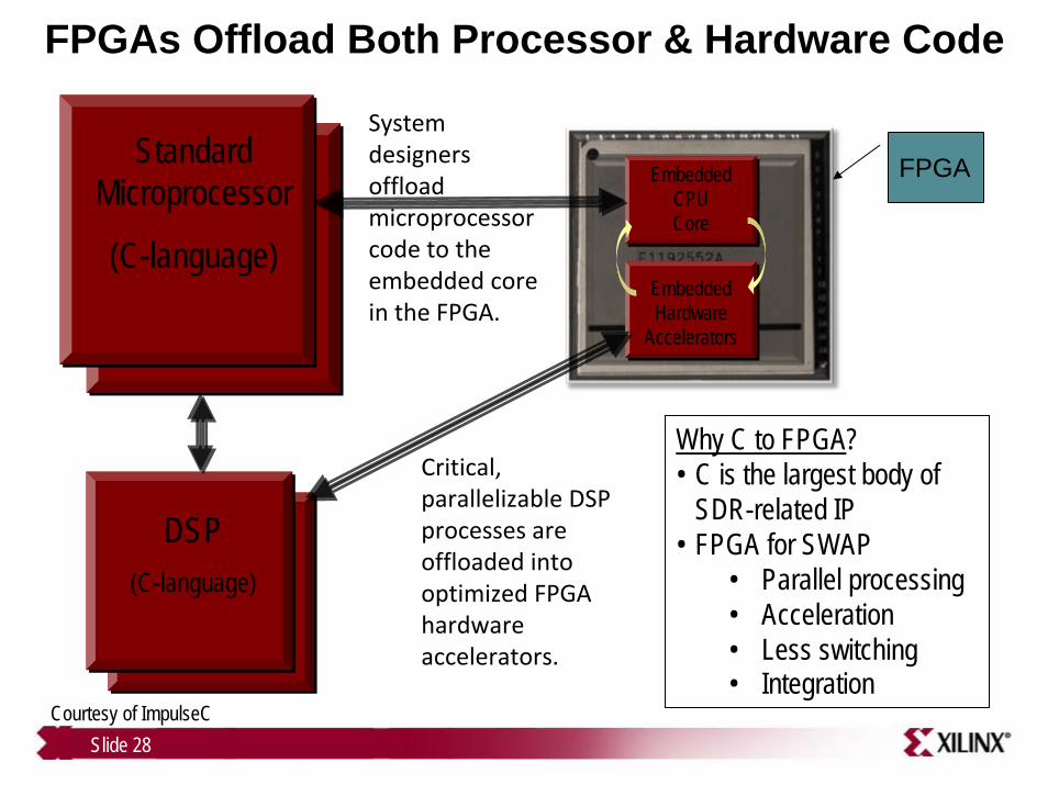
FPGAs Offload Both Processor & Hardware Code
DSP(C-language)
StandardMicroprocessor
(C-language)EmbeddedHardware
Accelerators
EmbeddedCPUCore
Critical, parallelizable DSP processes are offloaded into optimized FPGA hardware accelerators.
FPGA
System designers offload microprocessor code to the embedded core in the FPGA.
Why C to FPGA? • C is the largest body of
SDR-related IP • FPGA for SWAP
• Parallel processing• Acceleration• Less switching• Integration
Courtesy of ImpulseC

Slide 29
SDR with Processors IntegratedAll can be programmed in ANSI C.
Device: MicroprocessorStrength: Single or dual channel processing with high memory access SDR Uses: Protocol management
Low-frequency waveform processing Transmit and Receive management
Device: DSP Strength: Single channel, higher performance signal manipulationSDR Uses: Mod/Demod
FEC Low and medium speed I/O processing
Device: FPGAStrength: High I/O, multi-process, with optimized logic elementsSDR Uses: Incoming signal, data (e.g. encryption) or image processing
Up/Down conversion Signal Filters

Slide 30
Each Device Has I/O & Speed Strength
Power also increases with speed and # of processes
I/O
Speed
Microprocessor
DSP
FPGA

Slide 31
FPGAs Parallelize in Time or # of Processes to Achieve Performance at
Lower Power
CSpatialparallelism
Temporalparallelism
(system‐level pipelining)
C
C
C
C
C
C
C
C

Slide 32
FPGA C Programming Model
Communicating C-Language ProcessesBuffered communication channels to implement data streamsSupports dataflow and message-based communicationsSupports parallelism at the application level and at the level of individual processes
S/W process
H/W process
H/W process
S/W process
H/W process
H/W accelerator
Processor
PERIPHERALS
FPGA bus
Impulse Ccompiler
Impulse Ccompiler
MEM
ORY
CC
C
CC

Slide 33
FPGA Co-Processing Partitioning Options
C-to-HDLHardwareModule
ApplicationHardware
Accelerator
HostProcessor
1
EmbeddedHardware
Accelerators
EmbeddedCPUCore
Accelerate an embedded CPUCreate a hardware module
Accelerate anexternal/host CPU
Option Option
2
3
Option

Slide 34
PowerPC 405(VxWorks)
PowerPC 405(VxWorks)
TEMACTEMAC
FCB_0FCB_0
IDCTIDCTYUV ColorYUV Color
Image FilterImage Filter
FCB_1FCB_1
APU_1APU_1
PowerPC 405(standalone)
PowerPC 405(standalone)
APU_0APU_0
PLB_
1PL
B_1
PLB_
0PL
B_0
TFTTFT
INTCINTC
BRAMBRAM
DDR2DDR2
UARTUART
GPIOGPIO
INTCINTC
BRAMBRAM
DDR2DDR2
UARTUART
SysACESysACE
Web serverand TFTdisplaycontrol
MPEG2decodingand filtering
Dual PowerPC Embedded Computing
Dual PowerPC AccelerationEmbedded web server, camera interface and accelerated filteringTwo PowerPC processors, both with Impulse C accelerationFeaturing the Xilinx ML410 development board and Virtex-4 FX60 FPGA

Slide 35
FCB_0FCB_0
Custom DSP FilterCustom DSP Filter
PowerPC 440PowerPC 440
APU_0APU_0 PLB_
0PL
B_0
GPIOGPIO
INTCINTC
BRAMBRAM
DDR2DDR2
UARTUART
SysACESysACE
DSP filterfunctionacceleratedUsing an FPGAcoprocessor
FPGA/DSP Co-Design Example MPEG2

Slide 36
FCB_0FCB_0
IDCTIDCTYUV ColorYUV Color
PowerPC 440PowerPC 440
APU_0APU_0
PLB_
0PL
B_0
TFTTFT
GPIOGPIO
INTCINTC
BRAMBRAM
DDR2DDR2
UARTUART
SysACESysACEMPEG2decodingand display
PowerPC Embedded Computing

Slide 37slide 37WWW.XILINX.COM Embedded World 2008 37
Accelerated Process Library Example Showing Simple DoublingMPEG Process Accelerated 2 – 8X Over CPU
Frame rate doubled by offloading critical computations to the FPGA

Slide 3838 www.ImpulseC.com
Example: FPGA Embedded SystemUsing Xilinx Virtex‐5 with MicroBlaze soft processor
JTAG BlockJTAG Block
System Reset
System Reset
Dual PortBlock RAMDual Port
Block RAMInstruction‐Side Local
Memory BusData‐Side Local Memory Bus
MACMACUSBUSBGPIOGPIOMulti Channel
MemoryController
Multi Channel MemoryController
DDR SDRAMDDR SDRAM
UARTUART
MicroBlaze
Custom h/waccelerator
Custom h/wacceleratorFSL
Inst LMB
Inst LMB
Data LM
BData LM
B
On‐Chip Peripheral Bus ‐ OPB
void img_proc(co_stream pixels_in, co_stream piint nPixel;. . .do {co_stream_open(pixels_in, O_RDONLY, INTco_stream_open(pixels_out, O_WRONLY, INwhile ( co_stream_read(pixels_in, &nPixel, si
. . .// Do a filtering operation here using standa. . .
co_stream_write(pixels_out, &nPixel, sizeo} co_stream_close(pixels_in);co_stream_close(pixels_out);
} while(1); // Run forever
}

Slide 3939 www.ImpulseC.com
Embedded Processor Acceleration
Streamingfilter
attachedto embedded
processor
Streamcomponent
Signalcomponent
“Port”interfaces
Generated bus interface
Generated bus interface
C codecompiled to
HDL
Memory I/Ointerfaces
GeneratedHardware
Component
Generated hardware module/peripheral
Embedded PowerPCor MicroBlaze processorrunning user application(includes Impulse C API)
co_streamco_signal
co_memory
C‐to‐FPGA
FPGAfilter
PowerPC
C softwareapplication
APU
Virtex‐4 FX
Other I/O

Slide 4040 www.ImpulseC.com
Host Processor Acceleration
Host processoracceleration
example
Streamcomponent
Signalcomponent
Generated host interface
Generated host interface
C codecompiled to
HDLMemory I/Ointerfaces
GeneratedHardwareComponent
Windows or Linuxhost computer
running user application(includes Impulse C API)
co_streamco_signal
co_memory
C‐to‐FPGA
FPGAaccelerator
Host computer
C softwareapplication
PCIe,PCI‐Xetc.
FPGA
H/Wdriverlayer

Slide 41
Impulse Flow
Familiar IDE Interface
Desktop simulationUsing standard C programming methods
Dataflow analysisIdentify bottlenecks
Graphical optimization analysis
Balance size and speed to meet performance goals
41www.ImpulseC.com

Slide 42 www.ImpulseC.com
void img_proc(co_stream pixels_in, co_stream pixels_out) {int nPixel;. . .do {co_stream_open(pixels_in, O_RDONLY, INT_TYPE(32));co_stream_open(pixels_out, O_WRONLY, INT_TYPE(32));while ( co_stream_read(pixels_in, &nPixel, sizeof(int)) == 0 ) {
. . .// Do a filtering operation here using standard C…. . .
co_stream_write(pixels_out, &nPixel, sizeof(int));} co_stream_close(pixels_in);co_stream_close(pixels_out);
} while(1); // Run forever}
Impulse C Streaming Process
Impulse CstreamingAPI functionscompileautomaticallyto generateprocessor busInterfaces.

Slide 43slide 4343 www.ImpulseC.com
Impulse C API Functions
co_memory_createco_memory_ptrco_memory_readblockco_memory_writeblock
co_process_configco_process_create
co_register_createco_register_getco_register_putco_register_readco_register_write
co_semaphore_createco_semaphore_releaseco_semaphore_wait
co_signal_createco_signal_postco_signal_wait
co_stream_closeco_stream_createco_stream_eosco_stream_openco_stream_readco_stream_read_nbco_stream_writeco_stream_write_nb
cosim_logwindow_createcosim_logwindow_fwritecosim_logwindow_initcosim_logwindow_write

Slide 4444 www.ImpulseC.com
void img_proc(co_signal start, co_memory datamem, co_signal done) {double A[ARRAYSIZE];double B[ARRAYSIZE];int32 status;int32 offset = 0;. . .do {co_signal_wait(start, (int32*)&status);co_memory_readblock(datamem, offset, A, ARRAYSIZE * sizeof(double));
. . .// Do some kind of computation here, perhaps calculating A[] into B[]. . .
co_memory_writeblock(datamem, offset, B, ARRAYSIZE * sizeof(double));co_signal_post(done, 0);
} while(1);}
Impulse C Shared Memory Process

Slide 45
Device Independent Libraries w/ SDRQuicker Results
Tie into C, the biggest body of IPEnsure that new libraries are portableOpen up the world of COTS FPGA/DSP/uP platforms to software engineers
Reduced RiskPreserve the value of the government’s investment in IPMake it much easier to jump to better hardware components as they emergeC as input and VHDL or Verilog as output links to wide array of tools
More Cooperation Between GroupsChips away at hardware incompatibility by linking to a compelling, standard body of IPIncreases COTS hardware compatibilityDefer hardware dependencies to later in the process and onto thehardware manufacturers

Slide 46
Embedded Computing for SDRCombine embedded processors with custom C-language accelerators
Example: FPGA with soft processor
Easily partition your application between the embedded processor and FPGA logic
Verify using standard C debugging tools
Optimize your application for high performance
Instruction‐Side Local Memory Bus
Data‐Side Local Memory Bus
MACMACUSBUSBGPIOGPIO MemoryControllerMemory
ControllerUARTUART
FSL
Inst L
MBIns
t LMB
Data
LMB
Data
LMB
On-Chip BusOn-Chip Bus
CustomC-languagehardwareFIR filter
CustomC-languagehardwareFIR filter
Dual PortBlock RAMDual Port
Block RAM
DDR SDRAMDDR SDRAM
Embedded processor

Slide 47
FPGA-Based PlatformsHow to match a platform to your project?
TYPE OF FPGAWhat resources are available for computation?
HOST PROCESSOREmbedded within the FPGA, discrete, or none at all?
BUS ARCHITECTUREHow is the FPGA connected to the processor?
OTHER PERIPHERALSWhat devices will the FPGA application be communicating with?
OPERATING SYSTEMFor the host processor?
How many types of platforms are there?UNLIMITED!
For embedded computingFor desktop prototypingFor high performance computingCustomized for specific applications
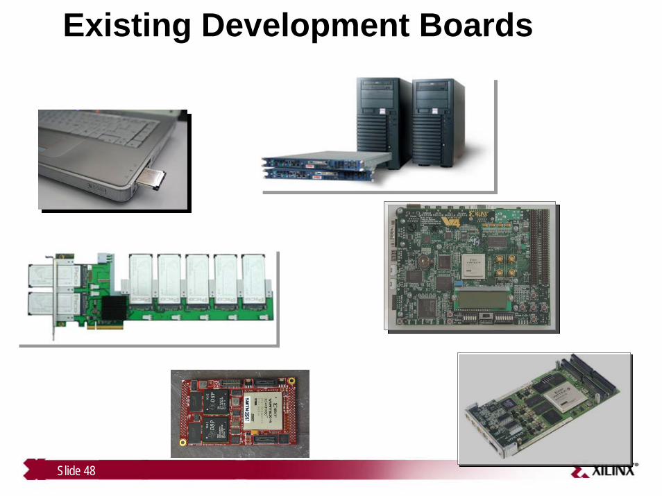
Slide 48
Existing Development Boards

Slide 49
Appendix 2: In-flight SDR• Slides Courtesy of SEAKR Engineering• Uses SRAM FPGAs
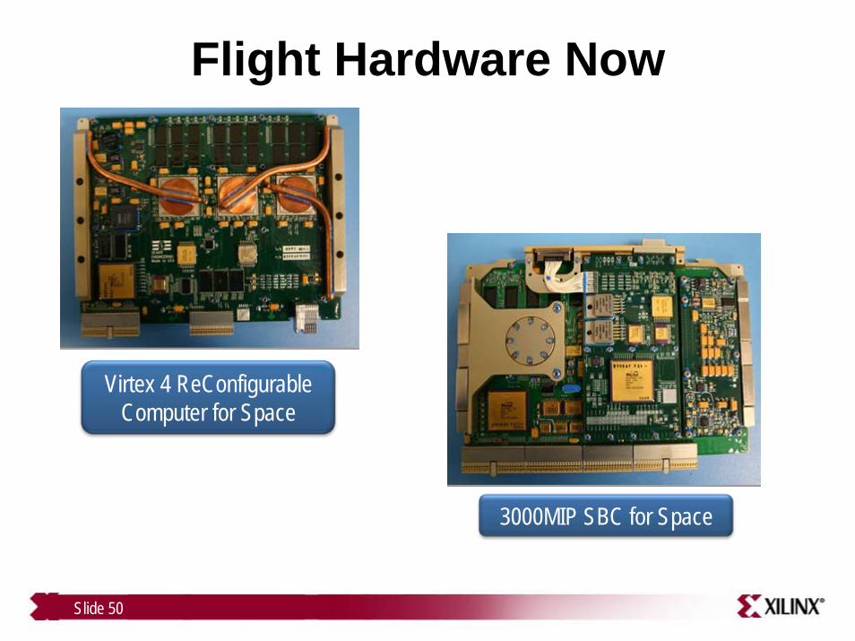
Slide 50
Flight Hardware Now
Virtex 4 ReConfigurableComputer for Space
3000MIP SBC for Space

Slide 51
Flight Hardware Now

Slide 52
RA-RCC Block Diagram
COP AXilinx V4 LX160
SRAM
FlashFlashFlash
PCI-PCIBridge / Config
LVDS I/O
PCI
DDR IISDRAMDDR II
SDRAMDDR IISDRAMDDR II
SDRAMDDR IISDRAMDDR II
SDRAM
SelectMap
256MB
cPCI High Speed Serial Network
COP BXilinx V4 LX160
DDR IISDRAMDDR II
SDRAMDDR IISDRAMDDR II
SDRAMDDR IISDRAMDDR II
SDRAM256MB
COP CXilinx V4 LX160
DDR IISDRAMDDR II
SDRAMDDR IISDRAMDDR II
SDRAMDDR IISDRAMDDR II
SDRAM256MB
LVDS I/O
LVDS I/O
High Speed Mezzanine
High Speed Mezzanine
High Speed Mezzanine
SRAMSDRAM

Slide 53
High Level Block Diagram
RC Processing
RC ProcessingRC
ProcessingRC
ProcessingRC Processing
RC ProcessingRC
ProcessingRC
Processing
GPPProcessing
GPPProcessingGPP
ProcessingGPP
ProcessingGPPProcessing
GPPProcessingGPP
ProcessingGPP
Processing
SEE Mitigation
RF OutRF In

Slide 54
SEE Mitigation, External TMR
• Pros:– SEFI Immune– SEU Immune (or very low)– “Brute force” approach, easy to
implement at the FPGA level– Protection for all internal resources
(macos, dcms, I/O)• Cons:
– Requires external device for majority voting
– Large SWAP increase– Requires design mods to eliminate
persistence and provide resynchronization logic FPGA B
ConfigBridge
FPGA BFPGA B
I/O Mezzanine
RCC
MajorityVoter
Non-TMRApplication
Non-TMRApplication
Non-TMRApplication

Slide 55
SEE Mitigation,Internal TMR Configuration
• Pros:– Fault tolerant design can be
implemented in a single FPGA• Reduce system SWAP
• Cons:– Difficult to implement– Design grows 3.4 to 6x– Speed decrease 5% to 20%– Power increase > 3x– Difficult/impossible to TMR some
embedded elements (PPC 405, SERDES)
– Not immune to SEFI’s– Has susceptible cross-section– MBUs may break internal TMR Config
Bridge
FPGA BFPGA B
RCC
FPGA BTMRApplication
TMRApplication
TMRApplication
DACADC DACADC DACADC
Slide 56
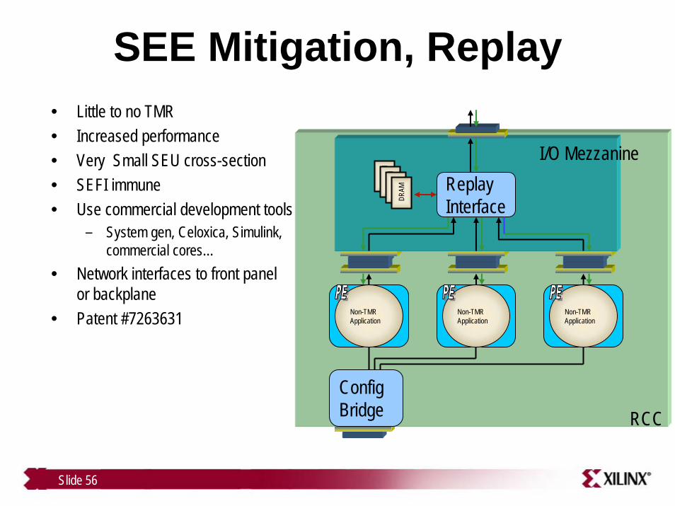
SEE Mitigation, Replay• Little to no TMR• Increased performance • Very Small SEU cross-section• SEFI immune• Use commercial development tools
– System gen, Celoxica, Simulink, commercial cores…
• Network interfaces to front panel or backplane
• Patent #7263631 FPGA B
ConfigBridge
FPGA BFPGA B
I/O Mezzanine
RCC
ReplayInterface
DRAM
DRAM
DRAM
DRAM
Non-TMRApplication
Non-TMRApplication
Non-TMRApplication

Slide 57
SEE Mitigation, Partial TMR
• Use selective TMR to remove persistence
• Data comes in through PCI or Mezzanine
• High processing performance
• Use commercial development tools
– System gen, Celoxica, Simulink, commercial cores…
– Designs require modification to remove persistence
ConfigBridge RCC
DACADC DACADC DACADC
PartialTMR
PartialTMR
PartialTMR
PartialTMR
PartialTMR
PartialTMR

Slide 58
SEE Mitigation, Hybrid TMR Configuration
• Non-TMR applications in all three FPGAs
• Third FPGA has a TMR’d Voter and TMR output
• Very small SEU cross-section
ConfigBridge
FPGA BFPGA B
RCC
TMRFPGA B
ADC ADC ADC
Non-TMRApplication
Non-TMRApplication
Non-TMRApplication

Slide 59
Space RCC Roadmap
1998 1999 2000 2001 2002 2003 2004 2005 2006 2007 2008 2009 2010
V1 RCC4M GatesVirtex 1 FPGABaseline RCC architecture
Perfo
rman
ce
V5-RCCVirtex 5TFlop ProcessingHSIO
AIP ProcessorVirtex 4Full or partial TMRDDRII SDRAM
V2 RCCVirtex 2DDRIINICMezzanine
SBR OBPVirtex 2 ProRIO NetworkNICQDR/DDR memory
Roadmap subject to change without notice
HRV RCCVirtex 2SDRAMMezzanine

Slide 60
Space SBC Roadmap
1998 1999 2000 2001 2002 2003 2004 2005 2006 2007 2008 2009 2010
MightySat IITI Quad C40250 MFLOP OBPHSI Cloud Detection
Perfo
rman
ce
Next GenerationTFlop ProcessingMulti GFLOPS/WattIn development
Athena ProcessorPowerPC Processor5.3 Gbyte/S memory bandwidth3000 MIPSECC on internal cache
SEAKR G4PowerPC Gen4800 MIPS2 GFLOPScPCISEAKR 603
PowerPC603e100 MIPSVME
Roadmap subject to change without notice


![317959 Mobile Opportunistic Traffic Offloading D5.1.2 ... · [A.2] D2.2.1 – General Architecture of the Mobile Offloading System [A.3] D3.1 – Initial results on offloading foundations](https://img.pdfslide.us/doc/110x75/5f0a455a7e708231d42ad72e/317959-mobile-opportunistic-traffic-offloading-d512-a2-d221-a-general.jpg)