Embed Size (px)
Citation preview
APPENDIX E
app00005 Dizi690 Demo Board
Chapter OutlineE.1. Circuit Design 397
E.2. Schematic Edit 398
E.3. Program Edit 401
E.4. Circuit Simulation 402
E.5. PCB Design 406
E.6. Package Assignment 407
E.7. Layout Edit 409
E.8. Output Files 411
E.9. PCB Fabrication 413
p0010 This appendix describes the process of developing a test board based on the PIC� 16F690
microcontroller (MCU), as used in the Microchip LPC (low pin count) demonstration board.
The design stages are:
• schematic capture with Labcenter ISIS
• interactive simulation with Labcenter Proteus VSM
• printed circuit board (PCB) design using Labcenter ARES
• PCB manufacture using Galaad Percival CNC software.
p0035 Proteus VSM has been used throughout this book as a design and debugging tool for PIC
microcontroller designs. Currently, a demonstration version may be downloaded which only
allows sample applications to be tested. For developing new designs, or testing those described in
this book, a suitable bundle containing PIC 16 models must be purchased from Labcenter
Electronics. For current product and demonstration software availability, refer towww.labcenter.
com. The design files for this test board can be downloaded from www.picmicros.org.uk.
s0010 E.1. Circuit Design
p0040 A target system was required which allowed basic PIC programming principles, as well as the
hardware development process, to be demonstrated. The following features are required:
• two push-button inputs (tactile switches, two inputs)
• 4-bit binary switched input (DIP switch, four inputs)
397
• one analogue input (manual pot, one analogue input)
• one-digit seven-segment display (LED, eight outputs including decimal point)
• sounder output (piezo transducer, one output).
In total, 16 input and output pins are required to meet this specification, and the number and
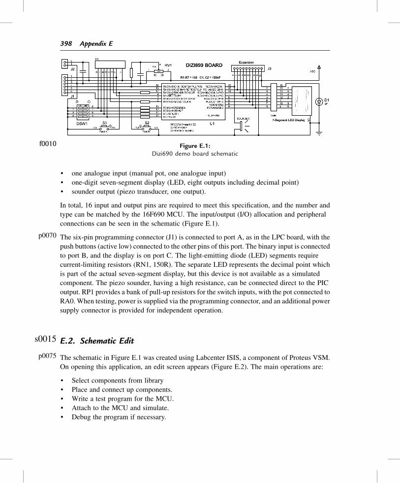
type can be matched by the 16F690 MCU. The input/output (I/O) allocation and peripheral
connections can be seen in the schematic (Figure E.1).
p0070 The six-pin programming connector (J1) is connected to port A, as in the LPC board, with the
push buttons (active low) connected to the other pins of this port. The binary input is connected
to port B, and the display is on port C. The light-emitting diode (LED) segments require
current-limiting resistors (RN1, 150R). The separate LED represents the decimal point which
is part of the actual seven-segment display, but this device is not available as a simulated
component. The piezo sounder, having a high resistance, can be connected direct to the PIC
output. RP1 provides a bank of pull-up resistors for the switch inputs, with the pot connected to
RA0. When testing, power is supplied via the programming connector, and an additional power
supply connector is provided for independent operation.
s0015 E.2. Schematic Edit
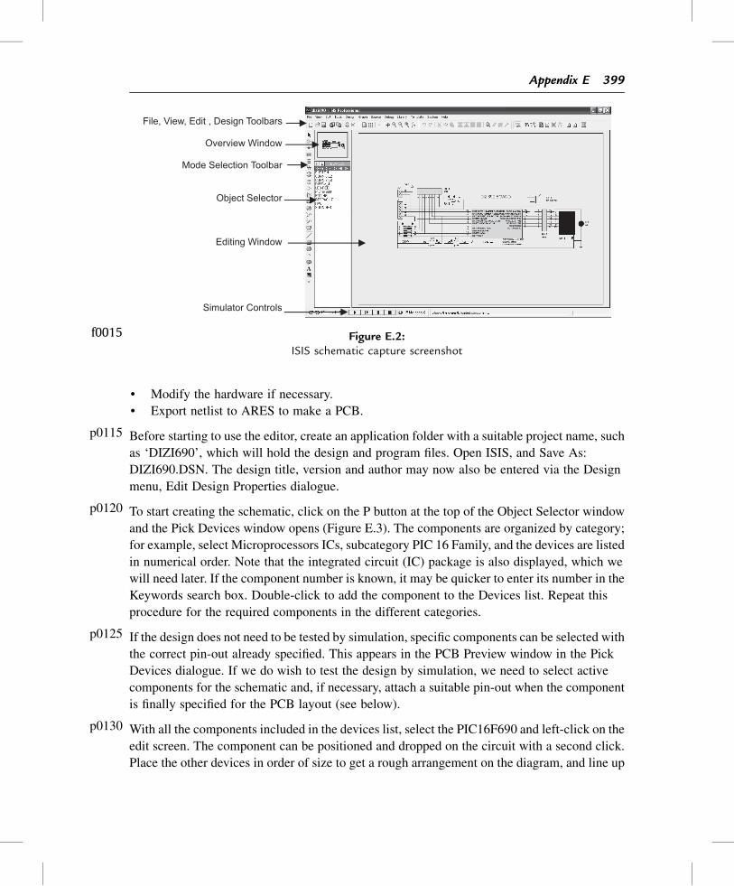
p0075 The schematic in Figure E.1 was created using Labcenter ISIS, a component of Proteus VSM.
On opening this application, an edit screen appears (Figure E.2). The main operations are:
• Select components from library
• Place and connect up components.
• Write a test program for the MCU.
• Attach to the MCU and simulate.
• Debug the program if necessary.
f0010 Figure E.1:Dizi690 demo board schematic
398 Appendix E
• Modify the hardware if necessary.
• Export netlist to ARES to make a PCB.
p0115 Before starting to use the editor, create an application folder with a suitable project name, such
as ‘DIZI690’, which will hold the design and program files. Open ISIS, and Save As:
DIZI690.DSN. The design title, version and author may now also be entered via the Design
menu, Edit Design Properties dialogue.
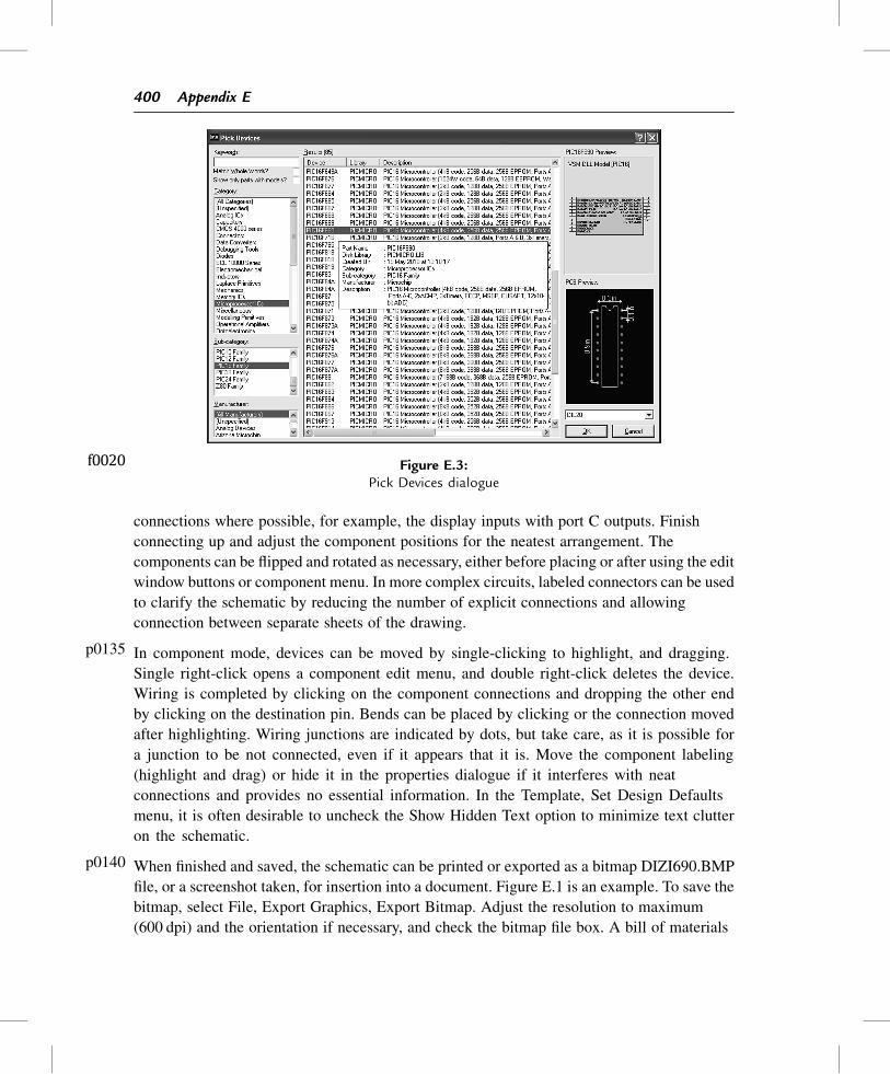
p0120 To start creating the schematic, click on the P button at the top of the Object Selector window
and the Pick Devices window opens (Figure E.3). The components are organized by category;
for example, select Microprocessors ICs, subcategory PIC 16 Family, and the devices are listed
in numerical order. Note that the integrated circuit (IC) package is also displayed, which we
will need later. If the component number is known, it may be quicker to enter its number in the
Keywords search box. Double-click to add the component to the Devices list. Repeat this
procedure for the required components in the different categories.
p0125 If the design does not need to be tested by simulation, specific components can be selected with
the correct pin-out already specified. This appears in the PCB Preview window in the Pick
Devices dialogue. If we do wish to test the design by simulation, we need to select active
components for the schematic and, if necessary, attach a suitable pin-out when the component
is finally specified for the PCB layout (see below).
p0130 With all the components included in the devices list, select the PIC16F690 and left-click on the
edit screen. The component can be positioned and dropped on the circuit with a second click.
Place the other devices in order of size to get a rough arrangement on the diagram, and line up
File, View, Edit , Design Toolbars
Overview Window
Mode Selection Toolbar
Object Selector
Editing Window
Simulator Controls
f0015 Figure E.2:ISIS schematic capture screenshot
Appendix E 399
connections where possible, for example, the display inputs with port C outputs. Finish
connecting up and adjust the component positions for the neatest arrangement. The
components can be flipped and rotated as necessary, either before placing or after using the edit
window buttons or component menu. In more complex circuits, labeled connectors can be used
to clarify the schematic by reducing the number of explicit connections and allowing
connection between separate sheets of the drawing.
p0135 In component mode, devices can be moved by single-clicking to highlight, and dragging.
Single right-click opens a component edit menu, and double right-click deletes the device.
Wiring is completed by clicking on the component connections and dropping the other end
by clicking on the destination pin. Bends can be placed by clicking or the connection moved
after highlighting. Wiring junctions are indicated by dots, but take care, as it is possible for
a junction to be not connected, even if it appears that it is. Move the component labeling
(highlight and drag) or hide it in the properties dialogue if it interferes with neat
connections and provides no essential information. In the Template, Set Design Defaults
menu, it is often desirable to uncheck the Show Hidden Text option to minimize text clutter
on the schematic.
p0140 When finished and saved, the schematic can be printed or exported as a bitmap DIZI690.BMP
file, or a screenshot taken, for insertion into a document. Figure E.1 is an example. To save the
bitmap, select File, Export Graphics, Export Bitmap. Adjust the resolution to maximum
(600 dpi) and the orientation if necessary, and check the bitmap file box. A bill of materials
f0020 Figure E.3:Pick Devices dialogue
400 Appendix E
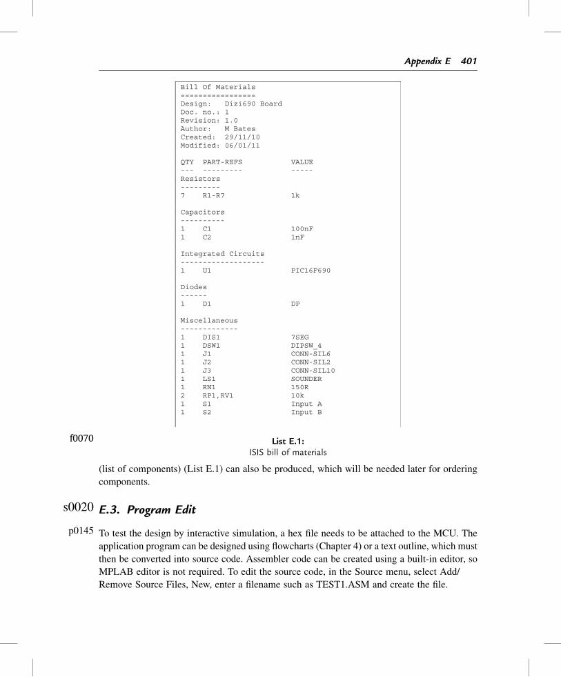
(list of components) (List E.1) can also be produced, which will be needed later for ordering
components.
s0020 E.3. Program Edit
p0145 To test the design by interactive simulation, a hex file needs to be attached to the MCU. The
application program can be designed using flowcharts (Chapter 4) or a text outline, which must
then be converted into source code. Assembler code can be created using a built-in editor, so
MPLAB editor is not required. To edit the source code, in the Source menu, select Add/
Remove Source Files, New, enter a filename such as TEST1.ASM and create the file.
Bill Of Materials ================= Design: Dizi690 Board Doc. no.: 1 Revision: 1.0 Author: M Bates Created: 29/11/10 Modified: 06/01/11
QTY PART-REFS VALUE --- --------- ----- Resistors --------- 7 R1-R7 1k
Capacitors ---------- 1 C1 100nF 1 C2 1nF
Integrated Circuits ------------------- 1 U1 PIC16F690
Diodes ------ 1 D1 DP
Miscellaneous ------------- 1 DIS1 7SEG 1 DSW1 DIPSW_4 1 J1 CONN-SIL6 1 J2 CONN-SIL2 1 J3 CONN-SIL10 1 LS1 SOUNDER 1 RN1 150R 2 RP1,RV1 10k 1 S1 Input A 1 S2 Input B
f0070 List E.1:ISIS bill of materials
Appendix E 401
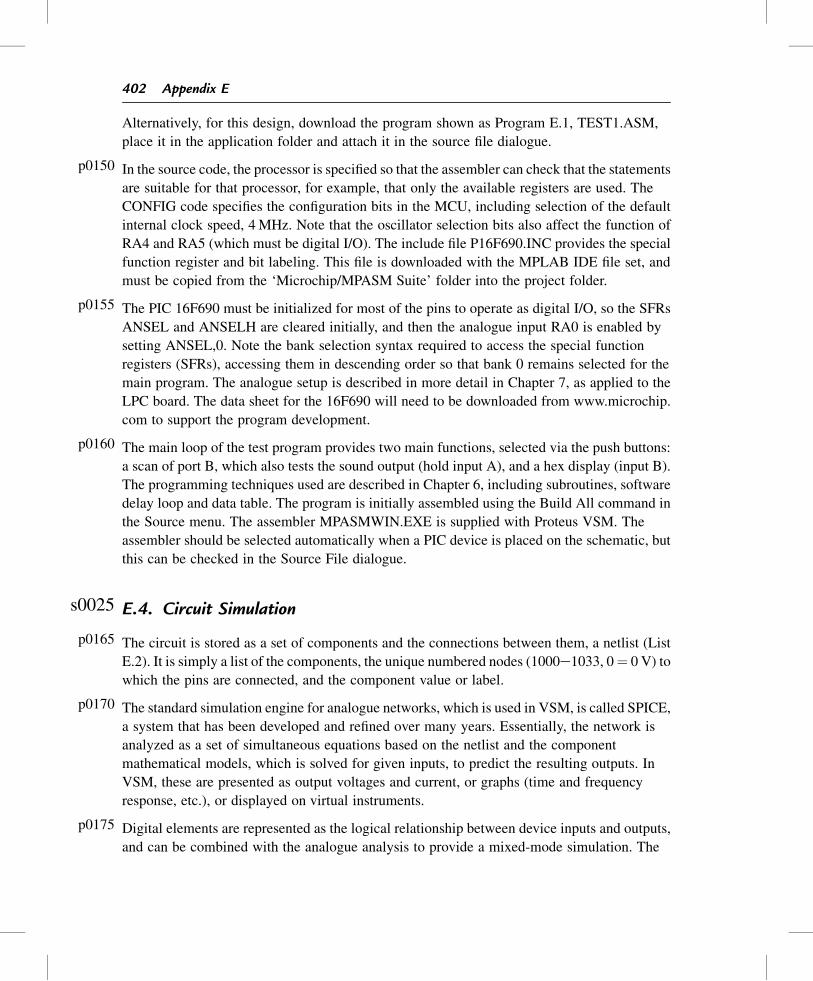
Alternatively, for this design, download the program shown as Program E.1, TEST1.ASM,
place it in the application folder and attach it in the source file dialogue.
p0150 In the source code, the processor is specified so that the assembler can check that the statements
are suitable for that processor, for example, that only the available registers are used. The
CONFIG code specifies the configuration bits in the MCU, including selection of the default
internal clock speed, 4 MHz. Note that the oscillator selection bits also affect the function of
RA4 and RA5 (which must be digital I/O). The include file P16F690.INC provides the special
function register and bit labeling. This file is downloaded with the MPLAB IDE file set, and
must be copied from the ‘Microchip/MPASM Suite’ folder into the project folder.
p0155 The PIC 16F690 must be initialized for most of the pins to operate as digital I/O, so the SFRs
ANSEL and ANSELH are cleared initially, and then the analogue input RA0 is enabled by
setting ANSEL,0. Note the bank selection syntax required to access the special function
registers (SFRs), accessing them in descending order so that bank 0 remains selected for the
main program. The analogue setup is described in more detail in Chapter 7, as applied to the
LPC board. The data sheet for the 16F690 will need to be downloaded from www.microchip.
com to support the program development.
p0160 The main loop of the test program provides two main functions, selected via the push buttons:
a scan of port B, which also tests the sound output (hold input A), and a hex display (input B).
The programming techniques used are described in Chapter 6, including subroutines, software
delay loop and data table. The program is initially assembled using the Build All command in
the Source menu. The assembler MPASMWIN.EXE is supplied with Proteus VSM. The
assembler should be selected automatically when a PIC device is placed on the schematic, but
this can be checked in the Source File dialogue.
s0025 E.4. Circuit Simulation
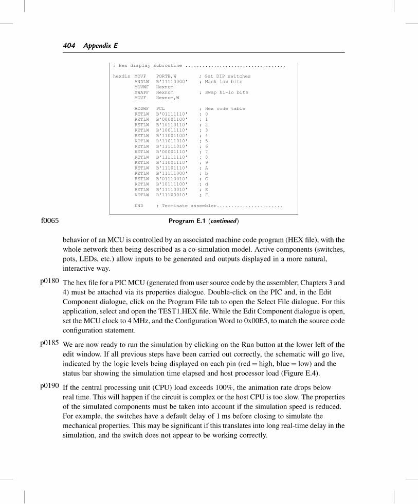
p0165 The circuit is stored as a set of components and the connections between them, a netlist (List
E.2). It is simply a list of the components, the unique numbered nodes (1000e1033, 0¼ 0 V) to
which the pins are connected, and the component value or label.
p0170 The standard simulation engine for analogue networks, which is used in VSM, is called SPICE,
a system that has been developed and refined over many years. Essentially, the network is
analyzed as a set of simultaneous equations based on the netlist and the component
mathematical models, which is solved for given inputs, to predict the resulting outputs. In
VSM, these are presented as output voltages and current, or graphs (time and frequency
response, etc.), or displayed on virtual instruments.
p0175 Digital elements are represented as the logical relationship between device inputs and outputs,
and can be combined with the analogue analysis to provide a mixed-mode simulation. The
402 Appendix E
;************************************************************; TEST1.ASM MPB Ver 1.0 ; Test program for DIZI690 demo board ; Status: Tested OK 6-1-11 ;;************************************************************
PROCESSOR 16F690 ; Specify MCU for assembler __CONFIG 00E5 ; MCU configuration bits ; PWRT on, MCLR enabled ; Internal Clock (default 4MHz) INCLUDE "P16F690.INC" ; Standard register labels
Loco EQU 20 ; Low count register Hico EQU 21 ; High count register Hexnum EQU 22 ; Hex table offset
; Initialise registers.......................................
BANKSEL ANSEL ; Select Bank 2 CLRF ANSEL ; Ports digital I/O BSF ANSEL,0 ; except AN0 Analogue input CLRF ANSELH ; Ports digital I/O
BANKSEL TRISC ; Select Bank 1 CLRF TRISC ; Port C for output MOVLW B'00010000' ; A/D clock setup code MOVWF ADCON1 ; A/D clock = fosc/8
BANKSEL PORTC ; Select bank 0 CLRF PORTC ; Clear display outputs MOVLW B'00000001' ; Analogue input setup code MOVWF ADCON0 ; Left justify, Vref=5V, ; Select RA0, done, enable A/D
; Main loop .................................................
buta BTFSC PORTA,2 ; Check button A GOTO butb ; ..and button B if off CLRF PORTC ; Clear display BSF PORTC,0 ; Switch on LSB
rotdis RLF PORTC ; Rotate segment CALL vardel ; Run variable delay BTFSS PORTA,2 ; Check button A again GOTO rotdis ; ..and continue if on
butb BTFSC PORTA,5 ; Else check button B GOTO buta ; ..and repeat if off CALL hexdis ; Get display code MOVWF PORTC ; Show it GOTO buta ; and repeat always
; Delay subroutine...........................................
vardel BSF ADCON0,1 ; start ADC.. wait BTFSC ADCON0,1 ; ..and wait for finish GOTO wait MOVF ADRESH,W ; Store result high byte MOVWF Hico INCF Hico ; Avoid zero count
slow CLRF Loco ; use result in delay fast DECFSZ Loco GOTO fast DECFSZ Hico GOTO slow RETURN ; done
f0065 Program E.1:Test program for Dizi690 board
Appendix E 403
behavior of an MCU is controlled by an associated machine code program (HEX file), with the
whole network then being described as a co-simulation model. Active components (switches,
pots, LEDs, etc.) allow inputs to be generated and outputs displayed in a more natural,
interactive way.
p0180 The hex file for a PICMCU (generated from user source code by the assembler; Chapters 3 and
4) must be attached via its properties dialogue. Double-click on the PIC and, in the Edit
Component dialogue, click on the Program File tab to open the Select File dialogue. For this
application, select and open the TEST1.HEX file. While the Edit Component dialogue is open,
set the MCU clock to 4MHz, and the Configuration Word to 0x00E5, to match the source code
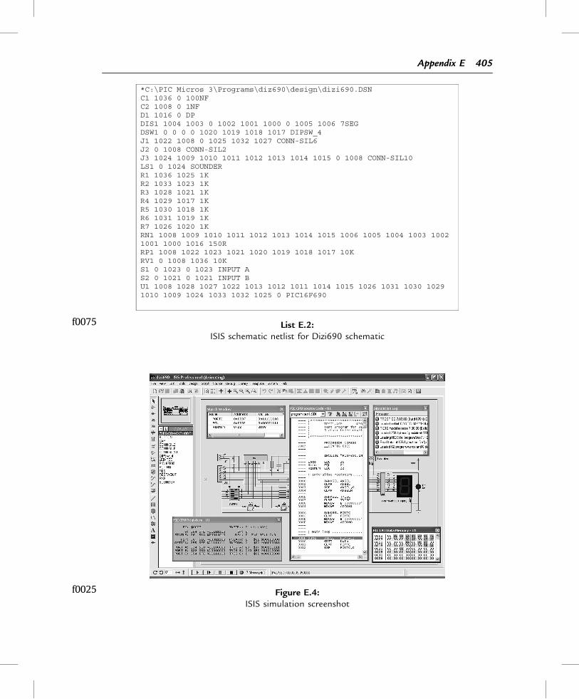
configuration statement.
p0185 We are now ready to run the simulation by clicking on the Run button at the lower left of the
edit window. If all previous steps have been carried out correctly, the schematic will go live,
indicated by the logic levels being displayed on each pin (red¼ high, blue¼ low) and the
status bar showing the simulation time elapsed and host processor load (Figure E.4).
p0190 If the central processing unit (CPU) load exceeds 100%, the animation rate drops below
real time. This will happen if the circuit is complex or the host CPU is too slow. The properties
of the simulated components must be taken into account if the simulation speed is reduced.
For example, the switches have a default delay of 1 ms before closing to simulate the
mechanical properties. This may be significant if this translates into long real-time delay in the
simulation, and the switch does not appear to be working correctly.
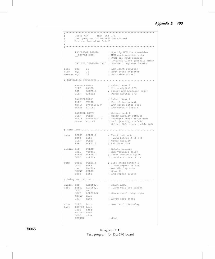
; Hex display subroutine ...................................
hexdis MOVF PORTB,W ; Get DIP switches ANDLW B'11110000' ; Mask low bits MOVWF Hexnum SWAPF Hexnum ; Swap hi-lo bits MOVF Hexnum,W
ADDWF PCL ; Hex code table RETLW B'01111110' ; 0 RETLW B'00001100' ; 1 RETLW B'10110110' ; 2 RETLW B'10011110' ; 3 RETLW B'11001100' ; 4 RETLW B'11011010' ; 5 RETLW B'11111010' ; 6 RETLW B'00001110' ; 7 RETLW B'11111110' ; 8 RETLW B'11001110' ; 9 RETLW B'11101110' ; A RETLW B'11111000' ; b RETLW B'01110010' ; C RETLW B'10111100' ; d RETLW B'11110010' ; E RETLW B'11100010' ; F
END ; Terminate assembler.......................
f0065 Program E.1 (continued)
404 Appendix E
*C:\PIC Micros 3\Programs\diz690\design\dizi690.DSN C1 1036 0 100NF C2 1008 0 1NF D1 1016 0 DP DIS1 1004 1003 0 1002 1001 1000 0 1005 1006 7SEG DSW1 0 0 0 0 1020 1019 1018 1017 DIPSW_4 J1 1022 1008 0 1025 1032 1027 CONN-SIL6 J2 0 1008 CONN-SIL2 J3 1024 1009 1010 1011 1012 1013 1014 1015 0 1008 CONN-SIL10 LS1 0 1024 SOUNDER R1 1036 1025 1K R2 1033 1023 1K R3 1028 1021 1K R4 1029 1017 1K R5 1030 1018 1K R6 1031 1019 1K R7 1026 1020 1K RN1 1008 1009 1010 1011 1012 1013 1014 1015 1006 1005 1004 1003 1002 1001 1000 1016 150R RP1 1008 1022 1023 1021 1020 1019 1018 1017 10K RV1 0 1008 1036 10K S1 0 1023 0 1023 INPUT A S2 0 1021 0 1021 INPUT B U1 1008 1028 1027 1022 1013 1012 1011 1014 1015 1026 1031 1030 1029 1010 1009 1024 1033 1032 1025 0 PIC16F690
f0075 List E.2:ISIS schematic netlist for Dizi690 schematic
f0025 Figure E.4:ISIS simulation screenshot
Appendix E 405

p0195 Stop resets the program simulation and Pause allows access to the debug menu options. The
CPU options are the most frequently used; the CPU source code, registers, data memory and
watch window are most useful (Figure E.4).
p0200 The source code window provides run, step and breakpoint controls. Step Into means execute
all instructions in sequence, Step Over means run subroutines below the current level at full
speed and Step Out allows us to leave a subroutine at full speed. Breakpoints are set by simply
double-clicking on the source code line, and the program will stop there. Using these controls,
the program sequence can be checked and particular sections scrutinized.
p0205 Register changes can be tracked via the register, data or a watch window; the latter has the
advantage that it remains visible during program execution at full speed. Registers to be
monitored are selected by right-clicking on the watch window. SFRs can be selected by
name, and user registers by number (user labels, unfortunately, are not recognized by the
debugger).
p0210 The animated schematic buttons can be operated in transient or toggle mode by clicking on the
button or the red dot control. The dual in-line (DIL) switches similarly can be controlled
individually or collectively. The pot is adjusted up and down via theþ and� dots. The sounder
outputs via the host sound card, and the display illuminates to demonstrate correct program
operation.
p0215 There are some components that have no simulation model, for example the connectors J1 and
J2. An error message will be displayed to this effect. The solution is to exclude them from the
simulation via their properties dialogue. Similarly, the discrete LED can be excluded from the
PCB layout because its function will be performed by the decimal point of the hardware
version of the component.
p0220 The main purpose of the simulation is software debugging. The relevant techniques are
outlined in Chapter 9. Normally, the source code window will be kept open during debugging
to make any changes necessary. After editing and saving any corrections, the program is
reassembled automatically when the Run button is pressed.
p0225 The interactive components provide a much more intuitive interface than the tabular output in
MPLAB, while the range of debugging and project management tools is fewer in Proteus VSM.
Normally, the hardware will be designed based on the application specification, then the
software, but it may be necessary to revisit the hardware in the light of program debugging.
s0030 E.5. PCB Design
p0230 When the circuit design has been completed in ISIS and firmware has been successfully tested,
the schematic netlist can be exported to the PCB layout package ARES.
406 Appendix E
p0235 To create a layout, a physical pin arrangement is needed for each component. The electrical
connections in the schematic have to be mapped onto the physical pins of the selected
component. This means that the real component must be selected and its pin-out specified both
electrically and physically. Some major components may need to be selected from a supplier’s
catalogue at this stage and the data sheet studied for this information.
p0240 Some pin-outs are already attached because the choice of package is limited to the available
component packages selected from the library. For example, the PIC 16F690 is only available
in a standard dual in-line (DIL), through-hole package, or one of three surface-mount
packages. For prototyping, the DIL package will be used, with a view to converting the PCB to
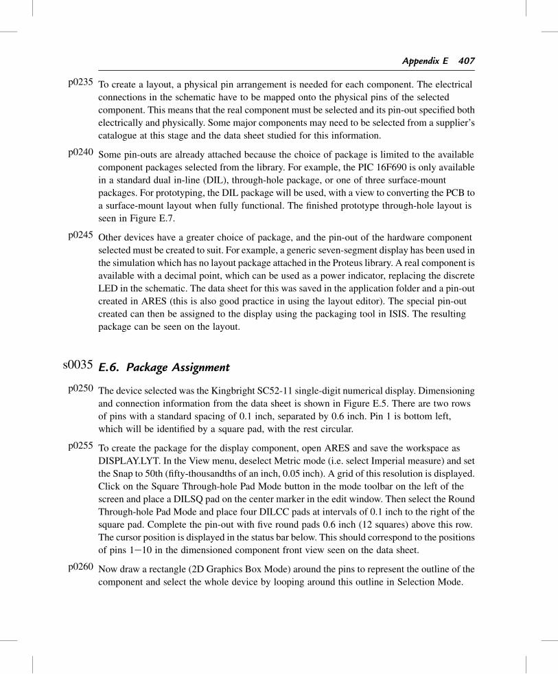
a surface-mount layout when fully functional. The finished prototype through-hole layout is
seen in Figure E.7.
p0245 Other devices have a greater choice of package, and the pin-out of the hardware component
selected must be created to suit. For example, a generic seven-segment display has been used in
the simulation which has no layout package attached in the Proteus library. A real component is
available with a decimal point, which can be used as a power indicator, replacing the discrete
LED in the schematic. The data sheet for this was saved in the application folder and a pin-out
created in ARES (this is also good practice in using the layout editor). The special pin-out
created can then be assigned to the display using the packaging tool in ISIS. The resulting
package can be seen on the layout.
s0035 E.6. Package Assignment
p0250 The device selected was the Kingbright SC52-11 single-digit numerical display. Dimensioning
and connection information from the data sheet is shown in Figure E.5. There are two rows
of pins with a standard spacing of 0.1 inch, separated by 0.6 inch. Pin 1 is bottom left,
which will be identified by a square pad, with the rest circular.
p0255 To create the package for the display component, open ARES and save the workspace as
DISPLAY.LYT. In the View menu, deselect Metric mode (i.e. select Imperial measure) and set
the Snap to 50th (fifty-thousandths of an inch, 0.05 inch). A grid of this resolution is displayed.
Click on the Square Through-hole Pad Mode button in the mode toolbar on the left of the
screen and place a DILSQ pad on the center marker in the edit window. Then select the Round
Through-hole Pad Mode and place four DILCC pads at intervals of 0.1 inch to the right of the
square pad. Complete the pin-out with five round pads 0.6 inch (12 squares) above this row.
The cursor position is displayed in the status bar below. This should correspond to the positions
of pins 1e10 in the dimensioned component front view seen on the data sheet.
p0260 Now draw a rectangle (2D Graphics Box Mode) around the pins to represent the outline of the
component and select the whole device by looping around this outline in Selection Mode.
Appendix E 407
Right-click on the highlighted package and Make Package. Give it a suitable name in the
dialogue (e.g. 7SEGDIS), and select the Package Category: Miscellaneous and Package Type:
Through Hole. It will be placed in the USERPKG library.
p0265 Now switch back to ISIS and assign packages to the other components where necessary. In the
case of the PIC, it is preassigned in the Proteus library. In the case of others, such as the pot and
tactile (push-button) switches, study the physical properties in component data sheet. A
suitable pin-out may, or may not, be found in the libraries, but it is relatively simple to make
one as described above for the display. The pin-out for the pot is fairly standard for a finger pot,
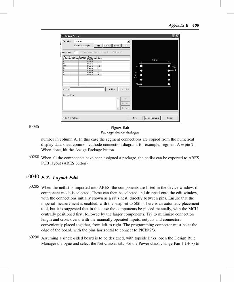
but the package for the switches had to be created.
p0270 If a component is placed in ISIS and the pins are already numbered, it implies that a package is
already attached (e.g. U1, J1, J2, J3, DSW1, RP1, RN1). If not, a package must be assigned, or
manufactured in ARES. It is attached by right-clicking on the component and selecting the
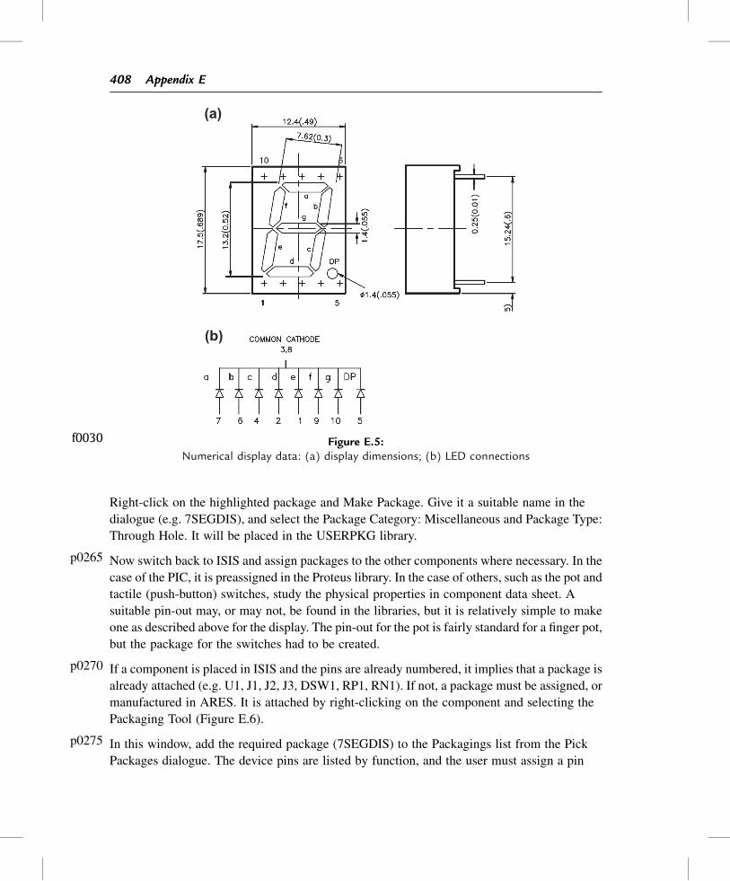
Packaging Tool (Figure E.6).
p0275 In this window, add the required package (7SEGDIS) to the Packagings list from the Pick
Packages dialogue. The device pins are listed by function, and the user must assign a pin
(a)
(b)
f0030 Figure E.5:Numerical display data: (a) display dimensions; (b) LED connections
408 Appendix E
number in column A. In this case the segment connections are copied from the numerical
display data sheet common cathode connection diagram, for example, segment A¼ pin 7.
When done, hit the Assign Package button.
p0280 When all the components have been assigned a package, the netlist can be exported to ARES
PCB layout (ARES button).
s0040 E.7. Layout Edit
p0285 When the netlist is imported into ARES, the components are listed in the device window, if
component mode is selected. These can then be selected and dropped onto the edit window,
with the connections initially shown as a rat’s nest, directly between pins. Ensure that the
imperial measurement is enabled, with the snap set to 50th. There is an automatic placement
tool, but it is suggested that in this case the components be placed manually, with the MCU
centrally positioned first, followed by the larger components. Try to minimize connection
length and cross-overs, with the manually operated inputs, outputs and connectors
conveniently placed together, from left to right. The programming connector must be at the
edge of the board, with the pins horizontal to connect to PICkit2/3.
p0290 Assuming a single-sided board is to be designed, with topside links, open the Design Rule
Manager dialogue and select the Net Classes tab. For the Power class, change Pair 1 (Hoz) to
f0035 Figure E.6:Package device dialogue
Appendix E 409
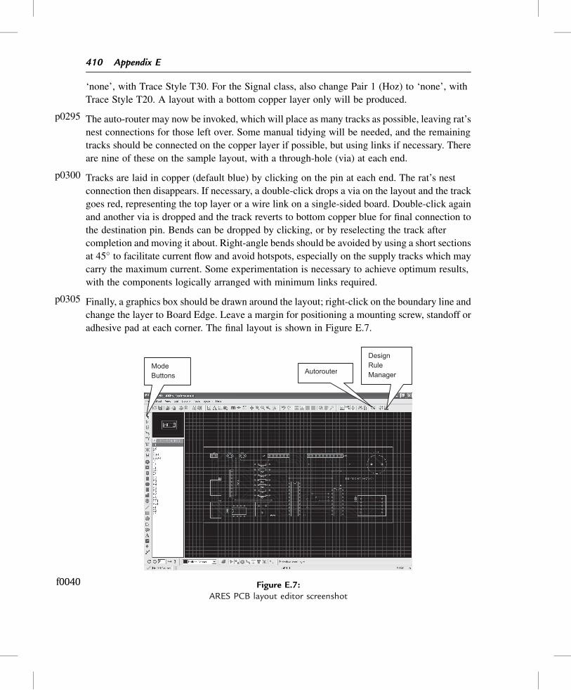
‘none’, with Trace Style T30. For the Signal class, also change Pair 1 (Hoz) to ‘none’, with
Trace Style T20. A layout with a bottom copper layer only will be produced.
p0295 The auto-router may now be invoked, which will place as many tracks as possible, leaving rat’s
nest connections for those left over. Some manual tidying will be needed, and the remaining
tracks should be connected on the copper layer if possible, but using links if necessary. There
are nine of these on the sample layout, with a through-hole (via) at each end.
p0300 Tracks are laid in copper (default blue) by clicking on the pin at each end. The rat’s nest
connection then disappears. If necessary, a double-click drops a via on the layout and the track
goes red, representing the top layer or a wire link on a single-sided board. Double-click again
and another via is dropped and the track reverts to bottom copper blue for final connection to
the destination pin. Bends can be dropped by clicking, or by reselecting the track after
completion and moving it about. Right-angle bends should be avoided by using a short sections
at 45� to facilitate current flow and avoid hotspots, especially on the supply tracks which may
carry the maximum current. Some experimentation is necessary to achieve optimum results,
with the components logically arranged with minimum links required.
p0305 Finally, a graphics box should be drawn around the layout; right-click on the boundary line and
change the layer to Board Edge. Leave a margin for positioning a mounting screw, standoff or
adhesive pad at each corner. The final layout is shown in Figure E.7.
Design Rule Manager Autorouter
Mode Buttons
f0040 Figure E.7:ARES PCB layout editor screenshot
410 Appendix E
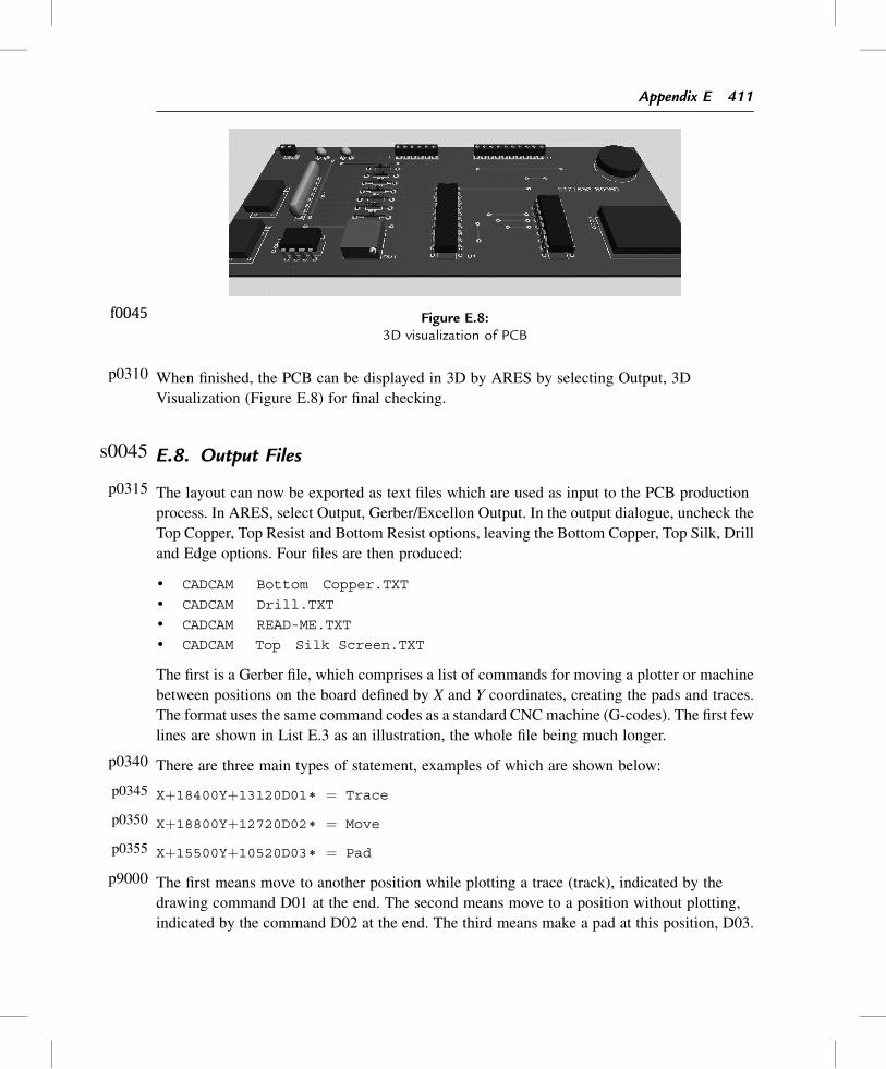
p0310 When finished, the PCB can be displayed in 3D by ARES by selecting Output, 3D
Visualization (Figure E.8) for final checking.
s0045 E.8. Output Files
p0315 The layout can now be exported as text files which are used as input to the PCB production
process. In ARES, select Output, Gerber/Excellon Output. In the output dialogue, uncheck the
Top Copper, Top Resist and Bottom Resist options, leaving the Bottom Copper, Top Silk, Drill
and Edge options. Four files are then produced:
• CADCAM Bottom Copper.TXT
• CADCAM Drill.TXT
• CADCAM READ-ME.TXT
• CADCAM Top Silk Screen.TXT
The first is a Gerber file, which comprises a list of commands for moving a plotter or machine
between positions on the board defined by X and Y coordinates, creating the pads and traces.
The format uses the same command codes as a standard CNC machine (G-codes). The first few
lines are shown in List E.3 as an illustration, the whole file being much longer.
p0340 There are three main types of statement, examples of which are shown below:
p0345 Xþ18400Yþ13120D01) ¼ Trace
p0350 Xþ18800Yþ12720D02) ¼ Move
p0355 Xþ15500Yþ10520D03) ¼ Pad
p9000 The first means move to another position while plotting a trace (track), indicated by the
drawing command D01 at the end. The second means move to a position without plotting,
indicated by the command D02 at the end. The third means make a pad at this position, D03.
f0045 Figure E.8:3D visualization of PCB
Appendix E 411
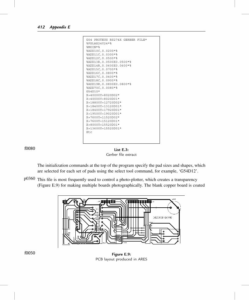
The initialization commands at the top of the program specify the pad sizes and shapes, which
are selected for each set of pads using the select tool command, for example, ‘G54D12’.
p0360 This file is most frequently used to control a photo-plotter, which creates a transparency
(Figure E.9) for making multiple boards photographically. The blank copper board is coated
G04 PROTEUS RS274X GERBER FILE* %FSLAX24Y24*% %MOIN*% %ADD10C,0.0200*% %ADD11C,0.0300*% %ADD12C,0.0500*% %ADD13R,0.0500X0.0500*% %ADD14R,0.0600X0.0600*% %ADD15C,0.0700*% %ADD16C,0.0800*% %ADD17C,0.0400*% %ADD18C,0.0900*% %ADD19R,0.0800X0.0800*% %ADD70C,0.0080*% G54D10* X+40000Y+8020D02* X+40000Y+8020D01* X+18800Y+12720D02* X+18400Y+13120D01* X+18400Y+17920D01* X+19500Y+19020D01* X+7600Y+11520D02* X+7600Y+15120D01* X+8000Y+15520D01* X+13600Y+15520D01* Etc
f0080 List E.3:Gerber file extract
f0050 Figure E.9:PCB layout produced in ARES
412 Appendix E

with an etch-resistant layer, which is photosensitive. When exposed to ultraviolet light through
the transparency, the exposed etch resist can be dissolved away, and the board developed by
etching away the copper in an acid solution where it has been exposed. This leaves the copper
traces and pads behind.
p0365 A cheaper way of achieving the same result is to send the layout as a bit map to a laser printer,
and print onto translucent drafting film. This can then be used as the photo-resist masking
image for the chemical etching process. This is the traditional method for hobbyists and
educational purposes. Note that the layout must be reversed for exposure.
p0370 An alternative process is to use the same file to control a milling machine, which will isolate
the tracks by machining around them with an engraving tool. This has the advantage of being
chemical (hazard) free, but is not as precise. However, it does have the major advantage that the
drilling operations (through holes) and milling (board edge) can be carried out on the same
machine by replacing the engraving tool with a drill or milling tool. The machining option is
probably best suited to making prototypes and small numbers of less complex boards. Such
machines are now available at lower cost for the hobby and education markets.
p0375 The Excellon format drill file is similar to the Gerber file, consisting principally of a list of X,Y
coordinates for each drill hole, with the drill sizes specified in the initialization code. The Top
Silk file also contains a list of coordinates, which control the plotting of the alphanumeric
characters to form the labeling of the components and connectors on the component (top) side
of the board. The Read-Me file has information about the file list, formatting options and
design information, since there is some variation in file formats and machine compatibility.
Since all these files are plain text, they can be opened in any text editor and the control codes
analyzed.
s0050 E.9. PCB Fabrication
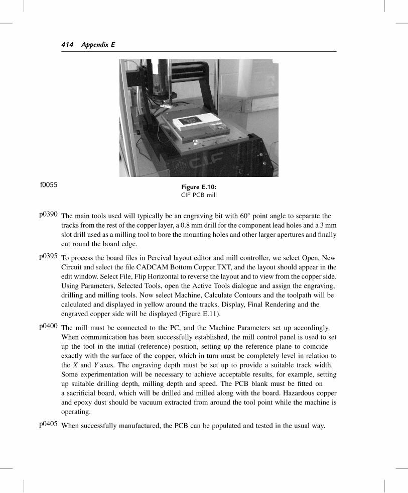
p0380 Low-cost 2.5D milling machines are now available which make the mechanical route to
a prototype PCB more attractive. They are basically an inexpensive drill attached to an XeY
plotter. Limited vertical movement (Z) is also needed to lift the engraving tool and implement
drilling operations. The software used here is Galaad Percival (www.galaad.net), designed to
control a CIF mill (Figure E.10). A demo version of the software can be downloaded for
experimentation; a dongle must be purchased to enable the machine interface.
p0385 Percival is loaded onto the host computer, which is attached to the mill via an RS232 link. It
takes the ARES output files, displays the layout and calculates the engraving tool path required
to make the PCB connections, and carry out the additional milling and drilling operations. This
will leave most of the copper in place, as a ground plane. Centering holes can be added at each
corner for mounting the board, if required.
Appendix E 413
p0390 The main tools used will typically be an engraving bit with 60� point angle to separate the
tracks from the rest of the copper layer, a 0.8 mm drill for the component lead holes and a 3 mm
slot drill used as a milling tool to bore the mounting holes and other larger apertures and finally
cut round the board edge.
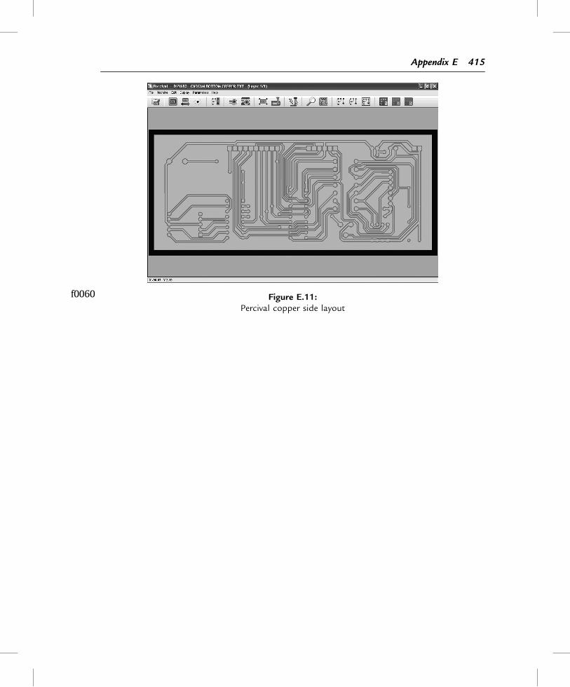
p0395 To process the board files in Percival layout editor and mill controller, we select Open, New
Circuit and select the file CADCAM Bottom Copper.TXT, and the layout should appear in the
edit window. Select File, Flip Horizontal to reverse the layout and to view from the copper side.
Using Parameters, Selected Tools, open the Active Tools dialogue and assign the engraving,
drilling and milling tools. Now select Machine, Calculate Contours and the toolpath will be
calculated and displayed in yellow around the tracks. Display, Final Rendering and the
engraved copper side will be displayed (Figure E.11).
p0400 The mill must be connected to the PC, and the Machine Parameters set up accordingly.
When communication has been successfully established, the mill control panel is used to set
up the tool in the initial (reference) position, setting up the reference plane to coincide
exactly with the surface of the copper, which in turn must be completely level in relation to
the X and Y axes. The engraving depth must be set up to provide a suitable track width.
Some experimentation will be necessary to achieve acceptable results, for example, setting
up suitable drilling depth, milling depth and speed. The PCB blank must be fitted on
a sacrificial board, which will be drilled and milled along with the board. Hazardous copper
and epoxy dust should be vacuum extracted from around the tool point while the machine is
operating.
p0405 When successfully manufactured, the PCB can be populated and tested in the usual way.
f0055 Figure E.10:CIF PCB mill
414 Appendix E
f0060 Figure E.11:Percival copper side layout
Appendix E 415


Non Print Items
Dizi690 Demo Board
Abstract: This appendix describes the process of developing a test board based on the
PIC 16F690 microcontroller, as used in the Microchip LPC demonstration board. Basic
PIC programming principles, as well as the hardware development process, are
demonstrated. The design stages are: schematic capture with Labcenter ISIS; inter-
active simulation with Labcenter Proteus VSM; printed circuit board (PCB) design
using Labcenter ARES; and PCB manufacture using Galaad Percival CNC software.
The layout can be exported as text files which are used as inputs to the PCB production
process. Once manufactured, the PCB can be populated and tested in the usual way.
Proteus VSM has been used throughout this book as a design and debugging tool for
PIC microcontroller designs. A demonstration version can be downloaded which
allows sample applications to be tested.
Key Words: circuit design; circuit layout; circuit simulation; Dizi690 demo board;
PCB design; PCB fabrication; PIC 16F690; program edit; schematic edit