Embed Size (px)
Citation preview
Data Sheet
APDS-9251-001Digital RGB, IR, and Ambient Light Sensor
Description
The Broadcom® APDS-9251-001 device uses four individual channels of red, green, blue, and IR (RGB+IR) in a specially designed matrix arrangement. This allows the device to have optimal angular response and accurate RGB spectral response with high lux accuracy over various light sources. APDS-9251-001 supports the I2C interface and has a programmable interrupt controller that frees up micro-controller resources.
The device detects light intensity under a variety of lighting conditions and through a variety of attenuation materials, including dark glass. APDS-9251-001 could be configured as ambient light sensor and RGB+IR Sensor. The color-sensing feature is useful in applications, such as LED RGB backlight control, solid-state lighting, reflected LED color sampler, or fluorescent light color temperature detection. The integrated IR blocking filter makes this device an excellent ambient light sensor and color temperature monitor sensor together with the temperature compensation that allows output to have less variation over the temperature.
Ordering Information
Features
RGB and ambient light sensing (RGB and ALS)
– Accuracy of correlated color temperature (CCT)
– Individual channels for red, green, blue, and infared
– Approximates human eye response with green channel
– Red, green, blue, infrared, and ALS sensing
– High sensitivity in low lux condition – ideally suited for operation behind dark glass
– Wide dynamic range: 18,000,000: 1
– Up to 20-bit resolution
Power management
– Low active current
– Low standby current
I2C-bus fast mode compatible interface
– Up to 400 kHz (I2C fast-mode)
– Dedicated interrupt pin
Small package L 2.0 mm × W 2.0 mm × H 0.65 mm
Applications OLED display control
RGB LED backlight control
Ambient light color temperature sensing
Part Number Packaging Quantity
APDS-9251-001 Tape and Reel 2500 per reel
Broadcom APDS-9251-001-DS101March 12, 2019
APDS-9251-001 Data Sheet Digital RGB, IR, and Ambient Light Sensor
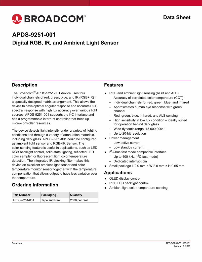
Functional Block Diagram
Description
The APDS-9251-001 device contains multiple photodiodes for light sensor (R, G, B, IR channel) that are designed in a matrix placement to achieve optimal angular response at the fall of incident light angle.
The device provides on-chip multiple diodes, ADCs, state machine, nonvolatile memory, and an I2C interface.
Integration of all color sensing channels occurs simultaneously. Upon completion of the conversion cycle, the conversion result is transferred to the corresponding data registers. Communication with the device is accomplished through a fast (up to 400 kHz), two-wire I2C serial bus for easy connection to a microcontroller or embedded controller.
The APDS-9251-001 provides a separate pin for interrupts. When interrupts are enabled and a preset value is exceeded, the interrupt pin is asserted and remains asserted until cleared by the controlling firmware. The interrupt feature simplifies and improves system efficiency by eliminating the need to poll a sensor for a light intensity. An interrupt is generated after completion of new conversion of the light sensor channels where the light sensor interrupt
source can work on any of the red, green, blue, or IR channels. Additionally, a programmable interrupt persistence feature allows the user to determine how many consecutive exceeded thresholds are necessary to trigger an interrupt.
I/O Pins Configuration
Pin Name Type Description
1 NC No connect
2 VDD Supply Power supply voltage
3 GND Ground Power supply ground. All voltages are referenced to GND
4 NC No connect
5 SCL I I2C serial clock input terminal. Clock
signal for I2C serial data.
6 SDA I/O Serial data I/O for I2C
7 INT O Interrupt. Open drain.
8 NC No connect
Broadcom APDS-9251-001-DS1012
APDS-9251-001 Data Sheet Digital RGB, IR, and Ambient Light Sensor
Absolute Maximum Ratings
Over operating free-air temperature range (see Note).
NOTE: Stresses beyond those listed under Absolute Maximum Ratings may cause permanent damage to the device. These are stress ratings only and functional operation of the device at these or any other conditions beyond those indicated under Recommended Operating Conditionsis not implied. Exposure to absolute-maximum-rated conditions for extended periods may affect device reliability.
Recommended Operating Conditions
Operating Characteristics
VDD = 2.8V, TA = 25°C (unless otherwise noted).
Parameter Symbol Min. Max. Units Conditions
Power Supply Voltagea
a. All voltages are with respect to GND.
VDD — 3.8 V
Digital Voltage Range –0.5 3.8 V
Storage Temperature Range Tstg –40 85 °C
Parameter Symbol Min. Typ. Max. Units
Operating Ambient Temperature TA –40 — 85 °C
Supply Voltage VDD 1.7 — 3.6 V
Supply Voltage Accuracy, VDD total error
including transients
–3 — 3 %
Parameter Symbol Min. Typ. Max. Units Test Conditions
Active Mode Current ICS — 130 — µA VDD = 2.8V, Gain Mode 3
Standby Current ISTBY — 1 2 µA In Standby Mode. No
active I2C communication
SCL, SDA Input High Voltage VIH 1.5 — VDD V
SCL, SDA Input Low Voltage VIL 0 — 0.4 V
VOL INT, Output Low Voltage VOL 0 — 0.4 V
ILEAK Leakage Current, SDA, SCL, INT
Pins
ILEAK –5 — 5 µA
Broadcom APDS-9251-001-DS1013
APDS-9251-001 Data Sheet Digital RGB, IR, and Ambient Light Sensor
Optical Characteristics
VDD = 2.8V, TA = 25°C (unless otherwise noted).
RGB Characteristics
VDD = 2.8V, TA = 25°C (unless otherwise noted).
ALS Characteristics
VDD = 2.8V, TA = 25°C (unless otherwise noted).
ParameterTest Condition
RED Channel Green Channel Blue Channel IR Channel
UnitMin. Max. Min. Max. Min. Max. Min. Max.
Irradiance Response
= 465a
a. The 465 nm input irradiance is supplied by an InGaN light-emitting diode with the following characteristics:dominant wavelength D = 465 nm, spectral halfwidth ½ = 22 nm.
0 5 6 20 80 120 0 4 %b
b. The percentage shown represents the ratio of the respective red, green, or blue channel value to the IR channel value.
= 525c
c. The 525 nm input irradiance is supplied by an InGaN light-emitting diode with the following characteristics: dominant wavelength D = 525 nm, spectral halfwidth ½ = 35 nm.
3 10 80 120 10 30 0 3
= 625d
d. The 625 nm input irradiance is supplied by a AlInGaP light-emitting diode with the following characteristics: dominant wavelength D = 625 nm, spectral halfwidth ½ = 15 nm.
80 120 18 37 0 3 0 3
= 850e
e. The 850 nm input irradiance is supplied by a AlInGaP light-emitting diode with the following characteristics: dominant wavelength D = 850 nm, spectral halfwidth ½ = 40 nm.
0 3 0 3 0 3 80 120
Parameter Min. Typ. Max. Units Test Conditions
Dark Count 0 — 3 counts
ADC Integration Time 2.97 3.125 3.28 ms
Full Scale ADC Counts Per Step — 8192 — counts 13 bit
Full Scale ADC Count Value — — 262,143 counts 18 bit, 100 ms, G = 1×
Parameter Symbol Min. Typ. Max. Units Test Conditions
Peak Wavelength P — 550 — nm
Min. Integration Time Tintmin1 — 3.125 — ms
Tintmin2 — 50 — ms With 50 Hz/60 Hz rejection
Max. Integration Time Tintmax — 400 — ms With 50 Hz/60 Hz rejection
Output Resolution RESALS 13 18 20 bit Programmable
ADC Count Value (Red) — 1000 — counts = 530 nm, 50 ms, Gain=3×,
Ee=62 µW/cm2
Broadcom APDS-9251-001-DS1014
APDS-9251-001 Data Sheet Digital RGB, IR, and Ambient Light Sensor
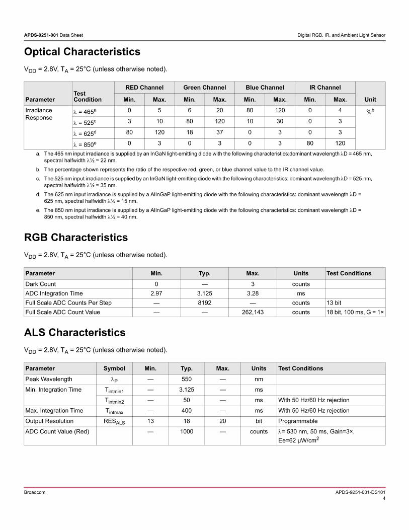
Figure 1: Normalized ALS PD Angular Response Figure 2: Nomalized PD Spectral Response
0
0.1
0.2
0.3
0.4
0.5
0.6
0.7
0.8
0.9
1
1.1
-90 -80 -70 -60 -50 -40 -30 -20 -10 0 10 20 30 40 50 60 70 80 90
NO
RM
ALI
ZED
RES
PO
NSI
VIT
Y
ANGULAR DISPLACEMENT (DEGREE)
0
0.1
0.2
0.3
0.4
0.5
0.6
0.7
0.8
0.9
1
300 400 500 600 700 800 900 1000 1100
REL
ATI
VE
RES
PO
NSE
WAVELENGTH (nm)
REDGREENBLUEIR
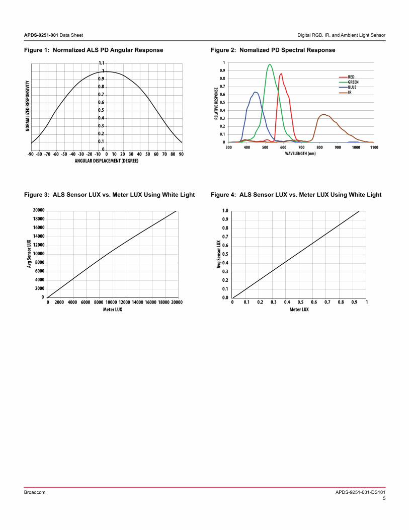
Figure 3: ALS Sensor LUX vs. Meter LUX Using White Light Figure 4: ALS Sensor LUX vs. Meter LUX Using White Light
0
2000
4000
6000
8000
10000
12000
14000
16000
18000
20000
0 2000 4000 6000 8000 10000 12000 14000 16000 18000 20000
Avg
Sen
sor
LUX
Meter LUX
0.0
0.1
0.2
0.3
0.4
0.5
0.6
0.7
0.8
0.9
1.0
0 0.1 0.2 0.3 0.4 0.5 0.6 0.7 0.8 0.9 1
Avg
Sen
sor
LUX
Meter LUX
Broadcom APDS-9251-001-DS1015
APDS-9251-001 Data Sheet Digital RGB, IR, and Ambient Light Sensor
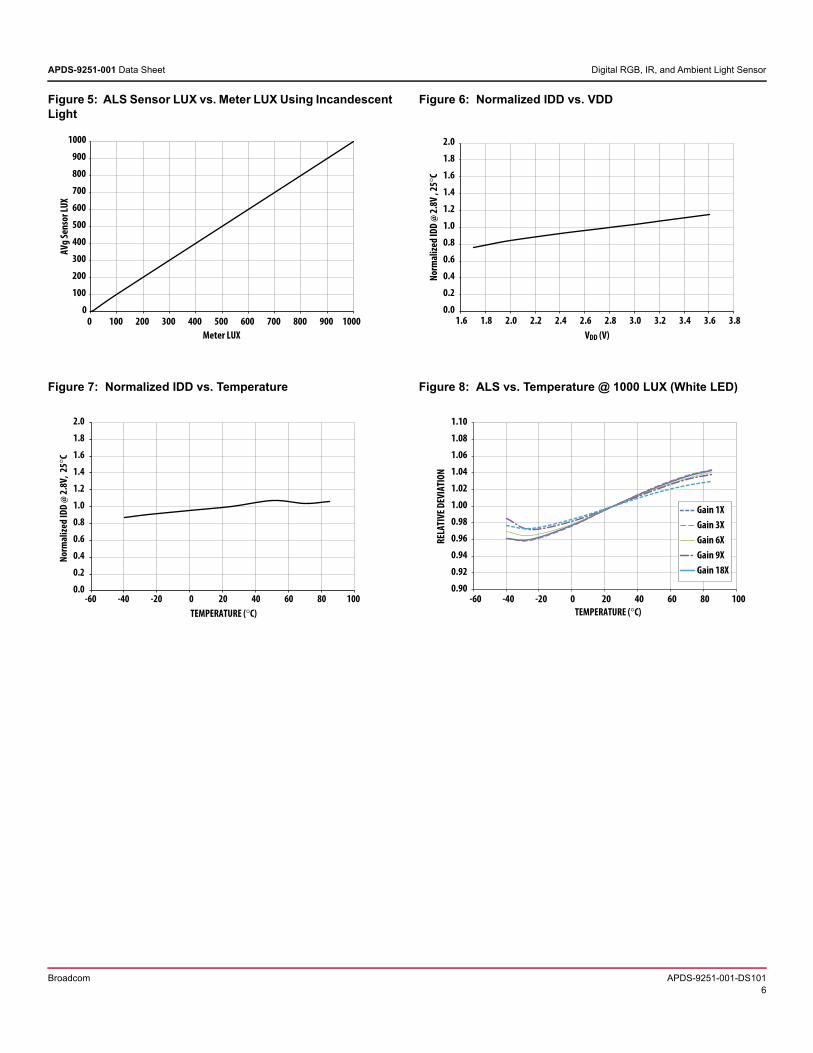
Figure 5: ALS Sensor LUX vs. Meter LUX Using Incandescent Light
Figure 6: Normalized IDD vs. VDD
0
100
200
300
400
500
600
700
800
900
1000
0 100 200 300 400 500 600 700 800 900 1000
AV
g Se
nso
r LU
X
Meter LUX
0.0
0.2
0.4
0.6
0.8
1.0
1.2
1.4
1.6
1.8
2.0
1.6 1.8 2.0 2.2 2.4 2.6 2.8 3.0 3.2 3.4 3.6 3.8
Nor
mal
ized
IDD
@ 2
.8V
, 25
C
VDD (V)
Figure 7: Normalized IDD vs. Temperature Figure 8: ALS vs. Temperature @ 1000 LUX (White LED)
0.0
0.2
0.4
0.6
0.8
1.0
1.2
1.4
1.6
1.8
2.0
-60 -40 -20 0 20 40 60 80 100
Nor
mal
ized
IDD
@ 2
.8V
, 25
C
TEMPERATURE ( C)
0.90
0.92
0.94
0.96
0.98
1.00
1.02
1.04
1.06
1.08
1.10
-60 -40 -20 0 20 40 60 80 100
REL
ATI
VE
DEV
IATI
ON
TEMPERATURE ( C)
Gain 1X
Gain 3X
Gain 6X
Gain 9X
Gain 18X
Broadcom APDS-9251-001-DS1016
APDS-9251-001 Data Sheet Digital RGB, IR, and Ambient Light Sensor
Principles of Operation for Light Sensor
System State Machine
Start Up after Power-On or Software Reset
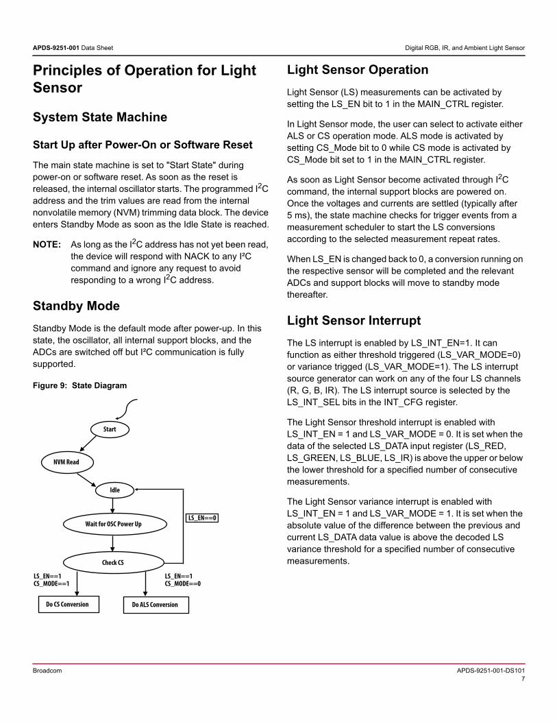
The main state machine is set to "Start State" during power-on or software reset. As soon as the reset is released, the internal oscillator starts. The programmed I2C address and the trim values are read from the internal nonvolatile memory (NVM) trimming data block. The device enters Standby Mode as soon as the Idle State is reached.
NOTE: As long as the I2C address has not yet been read, the device will respond with NACK to any I²C command and ignore any request to avoid responding to a wrong I2C address.
Standby Mode
Standby Mode is the default mode after power-up. In this state, the oscillator, all internal support blocks, and the ADCs are switched off but I²C communication is fully supported.
Figure 9: State Diagram
Light Sensor Operation
Light Sensor (LS) measurements can be activated by setting the LS_EN bit to 1 in the MAIN_CTRL register.
In Light Sensor mode, the user can select to activate either ALS or CS operation mode. ALS mode is activated by setting CS_Mode bit to 0 while CS mode is activated by CS_Mode bit set to 1 in the MAIN_CTRL register.
As soon as Light Sensor become activated through I2C command, the internal support blocks are powered on. Once the voltages and currents are settled (typically after 5 ms), the state machine checks for trigger events from a measurement scheduler to start the LS conversions according to the selected measurement repeat rates.
When LS_EN is changed back to 0, a conversion running on the respective sensor will be completed and the relevant ADCs and support blocks will move to standby mode thereafter.
Light Sensor Interrupt
The LS interrupt is enabled by LS_INT_EN=1. It can function as either threshold triggered (LS_VAR_MODE=0) or variance trigged (LS_VAR_MODE=1). The LS interrupt source generator can work on any of the four LS channels (R, G, B, IR). The LS interrupt source is selected by the LS_INT_SEL bits in the INT_CFG register.
The Light Sensor threshold interrupt is enabled with LS_INT_EN = 1 and LS_VAR_MODE = 0. It is set when the data of the selected LS_DATA input register (LS_RED, LS_GREEN, LS_BLUE, LS_IR) is above the upper or below the lower threshold for a specified number of consecutive measurements.
The Light Sensor variance interrupt is enabled with LS_INT_EN = 1 and LS_VAR_MODE = 1. It is set when the absolute value of the difference between the previous and current LS_DATA data value is above the decoded LS variance threshold for a specified number of consecutive measurements.
Start
NVM Read
Idle
Wait for OSC Power Up
Check CS
Do CS Conversion Do ALS Conversion
LS_EN==0
LS_EN==1CS_MODE==0
LS_EN==1CS_MODE==1
Broadcom APDS-9251-001-DS1017
APDS-9251-001 Data Sheet Digital RGB, IR, and Ambient Light Sensor
I2C Protocol
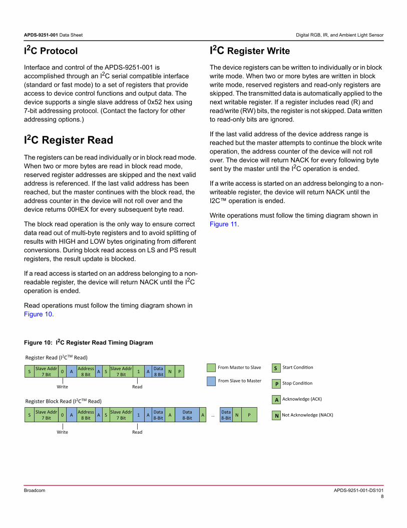
Interface and control of the APDS-9251-001 is accomplished through an I2C serial compatible interface (standard or fast mode) to a set of registers that provide access to device control functions and output data. The device supports a single slave address of 0x52 hex using 7-bit addressing protocol. (Contact the factory for other addressing options.)
I2C Register Read
The registers can be read individually or in block read mode. When two or more bytes are read in block read mode, reserved register addresses are skipped and the next valid address is referenced. If the last valid address has been reached, but the master continues with the block read, the address counter in the device will not roll over and the device returns 00HEX for every subsequent byte read.
The block read operation is the only way to ensure correct data read out of multi-byte registers and to avoid splitting of results with HIGH and LOW bytes originating from different conversions. During block read access on LS and PS result registers, the result update is blocked.
If a read access is started on an address belonging to a non-readable register, the device will return NACK until the I2C operation is ended.
Read operations must follow the timing diagram shown in Figure 10.
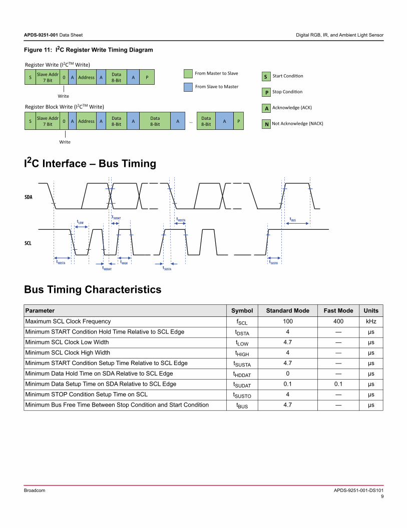
I2C Register Write
The device registers can be written to individually or in block write mode. When two or more bytes are written in block write mode, reserved registers and read-only registers are skipped. The transmitted data is automatically applied to the next writable register. If a register includes read (R) and read/write (RW) bits, the register is not skipped. Data written to read-only bits are ignored.
If the last valid address of the device address range is reached but the master attempts to continue the block write operation, the address counter of the device will not roll over. The device will return NACK for every following byte sent by the master until the I2C operation is ended.
If a write access is started on an address belonging to a non-writeable register, the device will return NACK until the I2C™ operation is ended.
Write operations must follow the timing diagram shown in Figure 11.
Figure 10: I2C Register Read Timing Diagram
Register Read (I2CTM Read)
S Slave Addr7 Bit 0 A Address
8 Bit A S Slave Addr7 Bit 1 A Data
8 Bit N P
S Slave Addr7 Bit 0 A Address
8 Bit A S Slave Addr7 Bit 1 A Data
8-Bit A Data 8-Bit A … Data
8-Bit N P
From Master to Slave
From Slave to Master
S
P
A
N
Start Condi on
Stop Condi on
Acknowledge (ACK)
Not Acknowledge (NACK)
ReadWrite
ReadWrite
Register Block Read (I2CTM Read)
Broadcom APDS-9251-001-DS1018
APDS-9251-001 Data Sheet Digital RGB, IR, and Ambient Light Sensor
Figure 11: I2C Register Write Timing Diagram
I2C Interface – Bus Timing
Bus Timing Characteristics
Parameter Symbol Standard Mode Fast Mode Units
Maximum SCL Clock Frequency fSCL 100 400 kHz
Minimum START Condition Hold Time Relative to SCL Edge tDSTA 4 — µs
Minimum SCL Clock Low Width tLOW 4.7 — µs
Minimum SCL Clock High Width tHIGH 4 — µs
Minimum START Condition Setup Time Relative to SCL Edge tSUSTA 4.7 — µs
Minimum Data Hold Time on SDA Relative to SCL Edge tHDDAT 0 — µs
Minimum Data Setup Time on SDA Relative to SCL Edge tSUDAT 0.1 0.1 µs
Minimum STOP Condition Setup Time on SCL tSUSTO 4 — µs
Minimum Bus Free Time Between Stop Condition and Start Condition tBUS 4.7 — µs
S Slave Addr7 Bit 0 A Address A Data
8-Bit A P
S Slave Addr7 Bit 0 A Address A Data
8-Bit A Data 8-Bit A … Data
8-Bit A P
Write
Write
Register Write (I2CTM Write)From Master to Slave
From Slave to Master
S
P
A
N
Start Condi on
Stop Condi on
Acknowledge (ACK)
Not Acknowledge (NACK)
Register Block Write (I2CTM Write)
SDA
SCL
tLOW
tHDSTA
tBUStHDSTAtSUDAT
tSUSTO
tSUSTA
tHIGH
tHDDAT
Broadcom APDS-9251-001-DS1019
APDS-9251-001 Data Sheet Digital RGB, IR, and Ambient Light Sensor
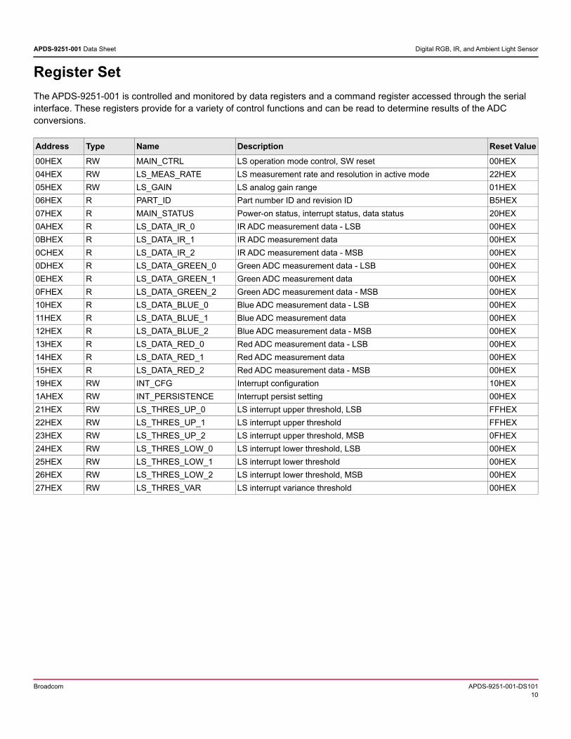
Register Set
The APDS-9251-001 is controlled and monitored by data registers and a command register accessed through the serial interface. These registers provide for a variety of control functions and can be read to determine results of the ADC conversions.
Address Type Name Description Reset Value
00HEX RW MAIN_CTRL LS operation mode control, SW reset 00HEX
04HEX RW LS_MEAS_RATE LS measurement rate and resolution in active mode 22HEX
05HEX RW LS_GAIN LS analog gain range 01HEX
06HEX R PART_ID Part number ID and revision ID B5HEX
07HEX R MAIN_STATUS Power-on status, interrupt status, data status 20HEX
0AHEX R LS_DATA_IR_0 IR ADC measurement data - LSB 00HEX
0BHEX R LS_DATA_IR_1 IR ADC measurement data 00HEX
0CHEX R LS_DATA_IR_2 IR ADC measurement data - MSB 00HEX
0DHEX R LS_DATA_GREEN_0 Green ADC measurement data - LSB 00HEX
0EHEX R LS_DATA_GREEN_1 Green ADC measurement data 00HEX
0FHEX R LS_DATA_GREEN_2 Green ADC measurement data - MSB 00HEX
10HEX R LS_DATA_BLUE_0 Blue ADC measurement data - LSB 00HEX
11HEX R LS_DATA_BLUE_1 Blue ADC measurement data 00HEX
12HEX R LS_DATA_BLUE_2 Blue ADC measurement data - MSB 00HEX
13HEX R LS_DATA_RED_0 Red ADC measurement data - LSB 00HEX
14HEX R LS_DATA_RED_1 Red ADC measurement data 00HEX
15HEX R LS_DATA_RED_2 Red ADC measurement data - MSB 00HEX
19HEX RW INT_CFG Interrupt configuration 10HEX
1AHEX RW INT_PERSISTENCE Interrupt persist setting 00HEX
21HEX RW LS_THRES_UP_0 LS interrupt upper threshold, LSB FFHEX
22HEX RW LS_THRES_UP_1 LS interrupt upper threshold FFHEX
23HEX RW LS_THRES_UP_2 LS interrupt upper threshold, MSB 0FHEX
24HEX RW LS_THRES_LOW_0 LS interrupt lower threshold, LSB 00HEX
25HEX RW LS_THRES_LOW_1 LS interrupt lower threshold 00HEX
26HEX RW LS_THRES_LOW_2 LS interrupt lower threshold, MSB 00HEX
27HEX RW LS_THRES_VAR LS interrupt variance threshold 00HEX
Broadcom APDS-9251-001-DS10110
APDS-9251-001 Data Sheet Digital RGB, IR, and Ambient Light Sensor
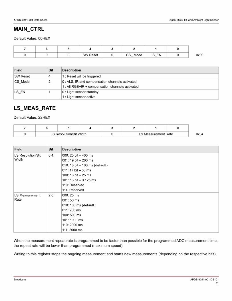
MAIN_CTRL
Default Value: 00HEX
LS_MEAS_RATE
Default Value: 22HEX
When the measurement repeat rate is programmed to be faster than possible for the programmed ADC measurement time, the repeat rate will be lower than programmed (maximum speed).
Writing to this register stops the ongoing measurement and starts new measurements (depending on the respective bits).
7 6 5 4 3 2 1 0
0 0 0 SW Reset 0 CS_ Mode LS_EN 0 0x00
Field Bit Description
SW Reset 4 1 : Reset will be triggered
CS_Mode 2 0 : ALS, IR and compensation channels activated
1 : All RGB+IR + compensation channels activated
LS_EN 1 0 : Light sensor standby
1 : Light sensor active
7 6 5 4 3 2 1 0
0 LS Resolution/Bit Width 0 LS Measurement Rate 0x04
Field Bit Description
LS Resolution/Bit Width
6:4 000: 20 bit – 400 ms
001: 19 bit – 200 ms
010: 18 bit – 100 ms (default)
011: 17 bit – 50 ms
100: 16 bit – 25 ms
101: 13 bit – 3.125 ms
110: Reserved
111: Reserved
LS Measurement Rate
2:0 000: 25 ms
001: 50 ms
010: 100 ms (default)
011: 200 ms
100: 500 ms
101: 1000 ms
110: 2000 ms
111: 2000 ms
Broadcom APDS-9251-001-DS10111
APDS-9251-001 Data Sheet Digital RGB, IR, and Ambient Light Sensor
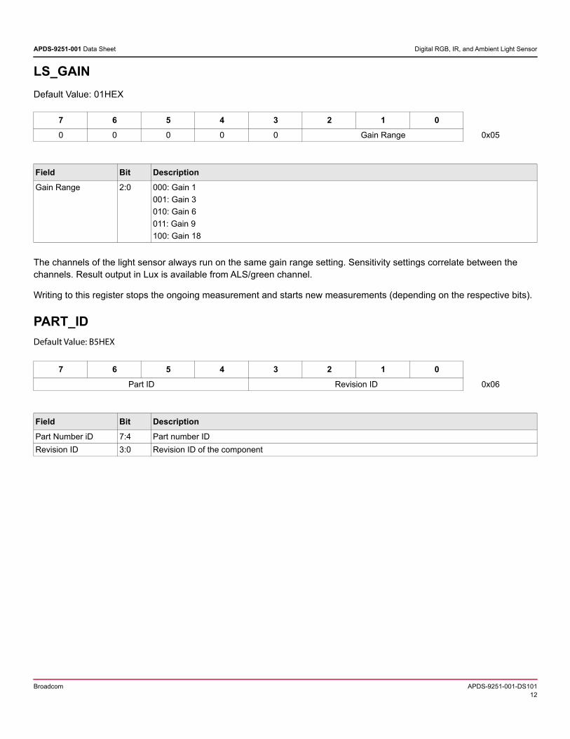
LS_GAIN
Default Value: 01HEX
The channels of the light sensor always run on the same gain range setting. Sensitivity settings correlate between the channels. Result output in Lux is available from ALS/green channel.
Writing to this register stops the ongoing measurement and starts new measurements (depending on the respective bits).
PART_ID
Default Value: B5HEX
7 6 5 4 3 2 1 0
0 0 0 0 0 Gain Range 0x05
Field Bit Description
Gain Range 2:0 000: Gain 1
001: Gain 3
010: Gain 6
011: Gain 9
100: Gain 18
7 6 5 4 3 2 1 0
Part ID Revision ID 0x06
Field Bit Description
Part Number iD 7:4 Part number ID
Revision ID 3:0 Revision ID of the component
Broadcom APDS-9251-001-DS10112
APDS-9251-001 Data Sheet Digital RGB, IR, and Ambient Light Sensor
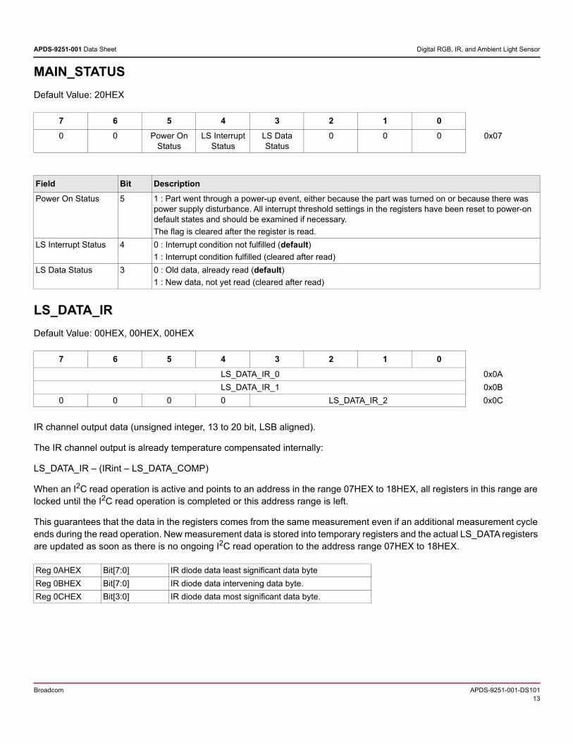
MAIN_STATUS
Default Value: 20HEX
LS_DATA_IR
Default Value: 00HEX, 00HEX, 00HEX
IR channel output data (unsigned integer, 13 to 20 bit, LSB aligned).
The IR channel output is already temperature compensated internally:
LS_DATA_IR – (IRint – LS_DATA_COMP)
When an I2C read operation is active and points to an address in the range 07HEX to 18HEX, all registers in this range are locked until the I2C read operation is completed or this address range is left.
This guarantees that the data in the registers comes from the same measurement even if an additional measurement cycle ends during the read operation. New measurement data is stored into temporary registers and the actual LS_DATA registers are updated as soon as there is no ongoing I2C read operation to the address range 07HEX to 18HEX.
7 6 5 4 3 2 1 0
0 0 Power On Status
LS Interrupt Status
LS Data Status
0 0 0 0x07
Field Bit Description
Power On Status 5 1 : Part went through a power-up event, either because the part was turned on or because there was power supply disturbance. All interrupt threshold settings in the registers have been reset to power-on default states and should be examined if necessary.
The flag is cleared after the register is read.
LS Interrupt Status 4 0 : Interrupt condition not fulfilled (default)
1 : Interrupt condition fulfilled (cleared after read)
LS Data Status 3 0 : Old data, already read (default)
1 : New data, not yet read (cleared after read)
7 6 5 4 3 2 1 0
LS_DATA_IR_0 0x0A
LS_DATA_IR_1 0x0B
0 0 0 0 LS_DATA_IR_2 0x0C
Reg 0AHEX Bit[7:0] IR diode data least significant data byte
Reg 0BHEX Bit[7:0] IR diode data intervening data byte.
Reg 0CHEX Bit[3:0] IR diode data most significant data byte.
Broadcom APDS-9251-001-DS10113
APDS-9251-001 Data Sheet Digital RGB, IR, and Ambient Light Sensor
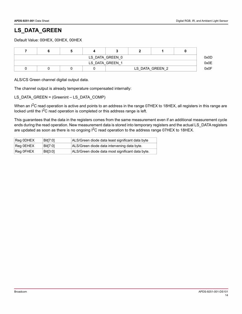
LS_DATA_GREEN
Default Value: 00HEX, 00HEX, 00HEX
ALS/CS Green channel digital output data.
The channel output is already temperature compensated internally:
LS_DATA_GREEN = (Greenint – LS_DATA_COMP)
When an I2C read operation is active and points to an address in the range 07HEX to 18HEX, all registers in this range are locked until the I2C read operation is completed or this address range is left.
This guarantees that the data in the registers comes from the same measurement even if an additional measurement cycle ends during the read operation. New measurement data is stored into temporary registers and the actual LS_DATA registers are updated as soon as there is no ongoing I2C read operation to the address range 07HEX to 18HEX.
7 6 5 4 3 2 1 0
LS_DATA_GREEN_0 0x0D
LS_DATA_GREEN_1 0x0E
0 0 0 0 LS_DATA_GREEN_2 0x0F
Reg 0DHEX Bit[7:0] ALS/Green diode data least significant data byte
Reg 0EHEX Bit[7:0] ALS/Green diode data intervening data byte.
Reg 0FHEX Bit[3:0] ALS/Green diode data most significant data byte.
Broadcom APDS-9251-001-DS10114
APDS-9251-001 Data Sheet Digital RGB, IR, and Ambient Light Sensor
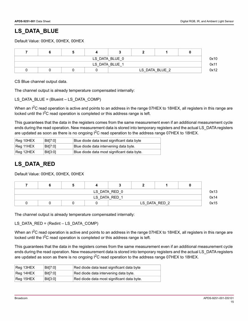
LS_DATA_BLUE
Default Value: 00HEX, 00HEX, 00HEX
CS Blue channel output data.
The channel output is already temperature compensated internally:
LS_DATA_BLUE = (Blueint – LS_DATA_COMP)
When an I2C read operation is active and points to an address in the range 07HEX to 18HEX, all registers in this range are locked until the I2C read operation is completed or this address range is left.
This guarantees that the data in the registers comes from the same measurement even if an additional measurement cycle ends during the read operation. New measurement data is stored into temporary registers and the actual LS_DATA registers are updated as soon as there is no ongoing I2C read operation to the address range 07HEX to 18HEX.
LS_DATA_RED
Default Value: 00HEX, 00HEX, 00HEX
The channel output is already temperature compensated internally:
LS_DATA_RED = (Redint – LS_DATA_COMP)
When an I2C read operation is active and points to an address in the range 07HEX to 18HEX, all registers in this range are locked until the I2C read operation is completed or this address range is left.
This guarantees that the data in the registers comes from the same measurement even if an additional measurement cycle ends during the read operation. New measurement data is stored into temporary registers and the actual LS_DATA registers are updated as soon as there is no ongoing I2C read operation to the address range 07HEX to 18HEX.
7 6 5 4 3 2 1 0
LS_DATA_BLUE_0 0x10
LS_DATA_BLUE_1 0x11
0 0 0 0 LS_DATA_BLUE_2 0x12
Reg 10HEX Bit[7:0] Blue diode data least significant data byte
Reg 11HEX Bit[7:0] Blue diode data intervening data byte.
Reg 12HEX Bit[3:0] Blue diode data most significant data byte.
7 6 5 4 3 2 1 0
LS_DATA_RED_0 0x13
LS_DATA_RED_1 0x14
0 0 0 0 LS_DATA_RED_2 0x15
Reg 13HEX Bit[7:0] Red diode data least significant data byte
Reg 14HEX Bit[7:0] Red diode data intervening data byte.
Reg 15HEX Bit[3:0] Red diode data most significant data byte.
Broadcom APDS-9251-001-DS10115
APDS-9251-001 Data Sheet Digital RGB, IR, and Ambient Light Sensor
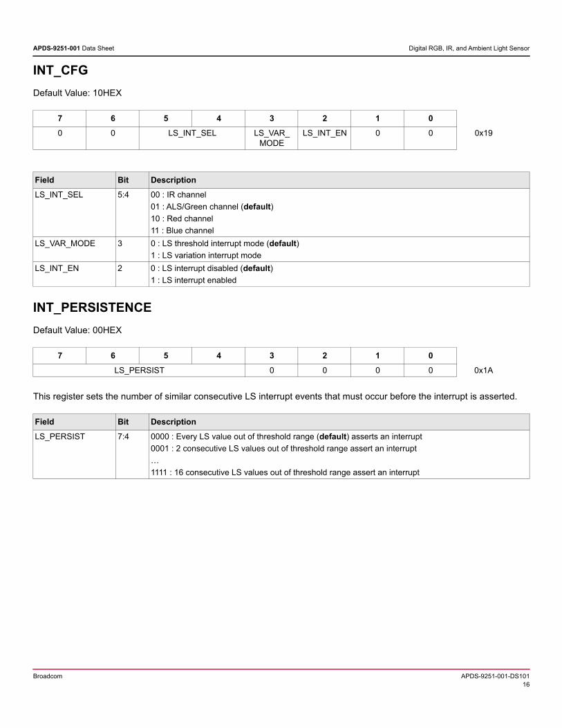
INT_CFG
Default Value: 10HEX
INT_PERSISTENCE
Default Value: 00HEX
This register sets the number of similar consecutive LS interrupt events that must occur before the interrupt is asserted.
7 6 5 4 3 2 1 0
0 0 LS_INT_SEL LS_VAR_ MODE
LS_INT_EN 0 0 0x19
Field Bit Description
LS_INT_SEL 5:4 00 : IR channel
01 : ALS/Green channel (default)
10 : Red channel
11 : Blue channel
LS_VAR_MODE 3 0 : LS threshold interrupt mode (default)
1 : LS variation interrupt mode
LS_INT_EN 2 0 : LS interrupt disabled (default)
1 : LS interrupt enabled
7 6 5 4 3 2 1 0
LS_PERSIST 0 0 0 0 0x1A
Field Bit Description
LS_PERSIST 7:4 0000 : Every LS value out of threshold range (default) asserts an interrupt
0001 : 2 consecutive LS values out of threshold range assert an interrupt
…
1111 : 16 consecutive LS values out of threshold range assert an interrupt
Broadcom APDS-9251-001-DS10116
APDS-9251-001 Data Sheet Digital RGB, IR, and Ambient Light Sensor
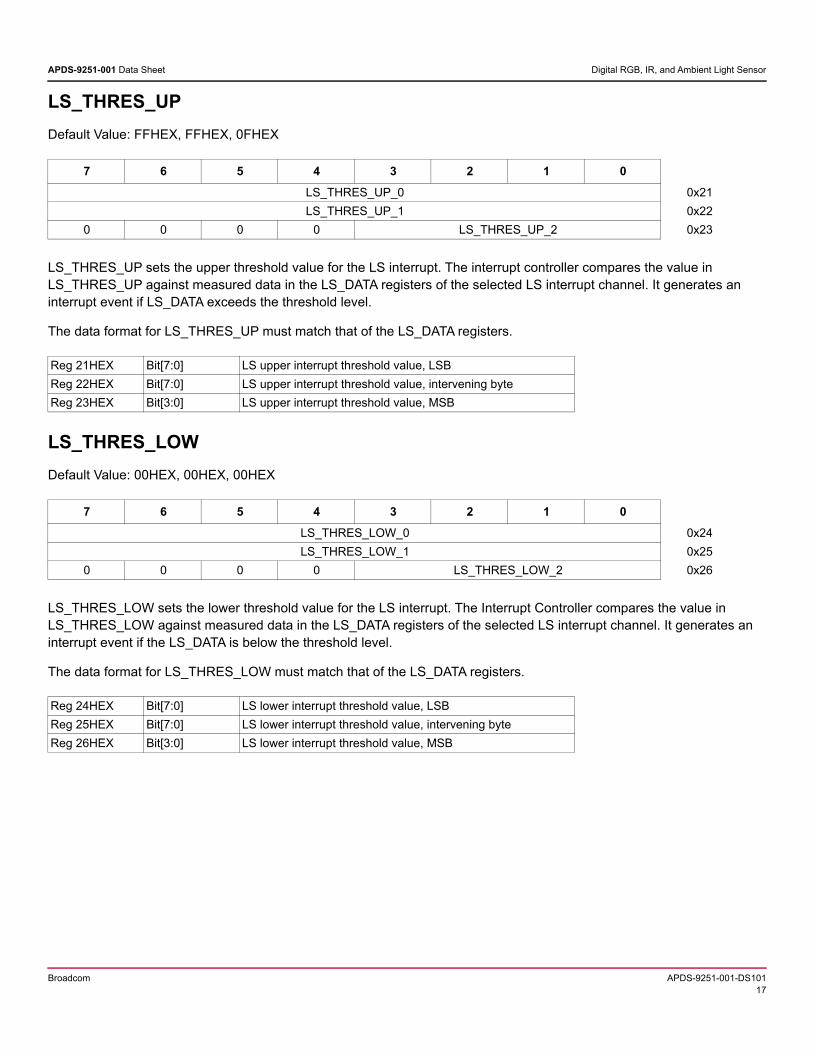
LS_THRES_UP
Default Value: FFHEX, FFHEX, 0FHEX
LS_THRES_UP sets the upper threshold value for the LS interrupt. The interrupt controller compares the value in LS_THRES_UP against measured data in the LS_DATA registers of the selected LS interrupt channel. It generates an interrupt event if LS_DATA exceeds the threshold level.
The data format for LS_THRES_UP must match that of the LS_DATA registers.
LS_THRES_LOW
Default Value: 00HEX, 00HEX, 00HEX
LS_THRES_LOW sets the lower threshold value for the LS interrupt. The Interrupt Controller compares the value in LS_THRES_LOW against measured data in the LS_DATA registers of the selected LS interrupt channel. It generates an interrupt event if the LS_DATA is below the threshold level.
The data format for LS_THRES_LOW must match that of the LS_DATA registers.
7 6 5 4 3 2 1 0
LS_THRES_UP_0 0x21
LS_THRES_UP_1 0x22
0 0 0 0 LS_THRES_UP_2 0x23
Reg 21HEX Bit[7:0] LS upper interrupt threshold value, LSB
Reg 22HEX Bit[7:0] LS upper interrupt threshold value, intervening byte
Reg 23HEX Bit[3:0] LS upper interrupt threshold value, MSB
7 6 5 4 3 2 1 0
LS_THRES_LOW_0 0x24
LS_THRES_LOW_1 0x25
0 0 0 0 LS_THRES_LOW_2 0x26
Reg 24HEX Bit[7:0] LS lower interrupt threshold value, LSB
Reg 25HEX Bit[7:0] LS lower interrupt threshold value, intervening byte
Reg 26HEX Bit[3:0] LS lower interrupt threshold value, MSB
Broadcom APDS-9251-001-DS10117
APDS-9251-001 Data Sheet Digital RGB, IR, and Ambient Light Sensor
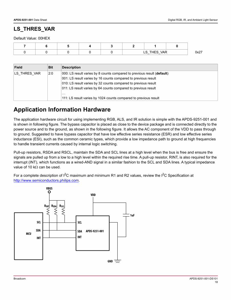
LS_THRES_VAR
Default Value: 00HEX
Application Information Hardware
The application hardware circuit for using implementing RGB, ALS, and IR solution is simple with the APDS-9251-001 and is shown in following figure. The bypass capacitor is placed as close to the device package and is connected directly to the power source and to the ground, as shown in the following figure. It allows the AC component of the VDD to pass through to ground. Suggested to have bypass capacitor that have low effective series resistance (ESR) and low effective series inductance (ESI), such as the common ceramic types, which provide a low impedance path to ground at high frequencies to handle transient currents caused by internal logic switching.
Pull-up resistors, RSDA and RSCL, maintain the SDA and SCL lines at a high level when the bus is free and ensure the signals are pulled up from a low to a high level within the required rise time. A pull-up resistor, RINT, is also required for the interrupt (INT), which functions as a wired-AND signal in a similar fashion to the SCL and SDA lines. A typical impedance value of 10 k can be used.
For a complete description of I2C maximum and minimum R1 and R2 values, review the I2C Specification at http://www.semiconductors.philips.com.
7 6 5 4 3 2 1 0
0 0 0 0 0 LS_THES_VAR 0x27
Field Bit Description
LS_THRES_VAR 2:0 000: LS result varies by 8 counts compared to previous result (default)
001: LS result varies by 16 counts compared to previous result
010: LS result varies by 32 counts compared to previous result
011: LS result varies by 64 counts compared to previous result
…
111: LS result varies by 1024 counts compared to previous result
MCU
SCL
SDA
INT
APDS-9251-001
SCL
SDA
INT
VDD
VBUS
RSDA RSCLRINT
GND
1uF
Broadcom APDS-9251-001-DS10118
APDS-9251-001 Data Sheet Digital RGB, IR, and Ambient Light Sensor
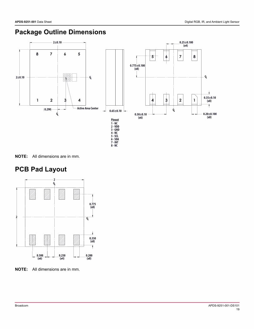
Package Outline Dimensions
NOTE: All dimensions are in mm.
PCB Pad Layout
NOTE: All dimensions are in mm.
2±0.10
2±0.10
0.290 Active Area Center
CL
CL 0.65±0.10
0.20±0.100(x8)
0.35±0.10(x8)
0.775±0.100(x8)
0.25±0.100(x4)
0.50±0.10(x6)
CL
CL
Pinout1 - NC2 - VDD3 - GND4 - NC5 - SCL6 - SDA7 - INT8 - NC
0.200(x8)
0.350(x8)
2
2
0.500(x6)
0.250(x4)
0.775(x8)
CL
CL
Broadcom APDS-9251-001-DS10119
APDS-9251-001 Data Sheet Digital RGB, IR, and Ambient Light Sensor
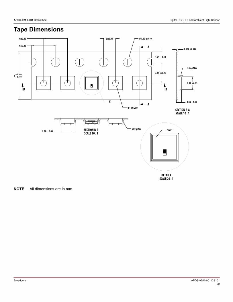
Tape Dimensions
NOTE: All dimensions are in mm.
8+-
0.3000.100
4 ±0.10
4 ±0.10 2 ±0.05 Ø 1.50 ±0.10
1.75 ±0.10
3.50 ±0.05
Ø 1 ±0.250
2.18 ±0.05 SECTION B-BSCALE 10 : 1
5 Deg Max
0.200 ±0.200
0.83 ±0.05
2.18 ±0.05
SECTION A-ASCALE 10 : 1
5 Deg Max
DETAIL CSCALE 20 : 1
Pin #1
BB
A
AC
Broadcom APDS-9251-001-DS10120
APDS-9251-001 Data Sheet Digital RGB, IR, and Ambient Light Sensor
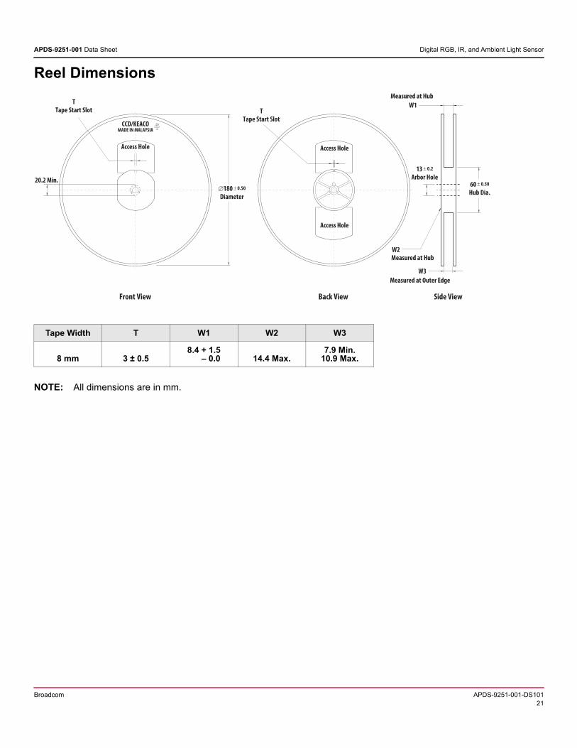
Reel Dimensions
NOTE: All dimensions are in mm.
Tape Width T W1 W2 W3
8 mm 3 ± 0.58.4 + 1.5
– 0.0 14.4 Max.7.9 Min.
10.9 Max.
13 0.2
Arbor Hole
W3
W1
180 0.50
Diameter
60 0.50
Hub Dia.
Access HoleAccess Hole
TTape Start Slot
TTape Start Slot
Access Hole
Measured at Outer Edge
W2Measured at Hub
Measured at Hub
20.2 Min.
CCD/KEACOMADE IN MALAYSIA
Front View Back View Side View
Broadcom APDS-9251-001-DS10121
APDS-9251-001 Data Sheet Digital RGB, IR, and Ambient Light Sensor
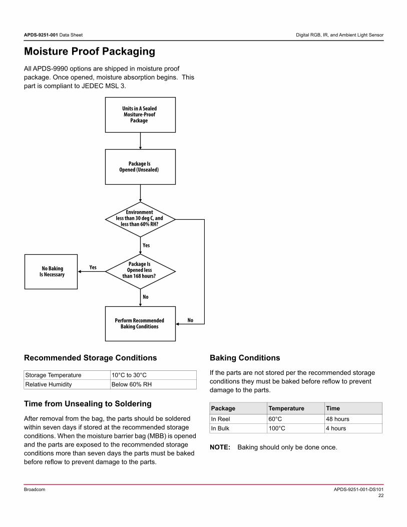
Moisture Proof Packaging
All APDS-9990 options are shipped in moisture proof package. Once opened, moisture absorption begins. This part is compliant to JEDEC MSL 3.
Recommended Storage Conditions
Time from Unsealing to Soldering
After removal from the bag, the parts should be soldered within seven days if stored at the recommended storage conditions. When the moisture barrier bag (MBB) is opened and the parts are exposed to the recommended storage conditions more than seven days the parts must be baked before reflow to prevent damage to the parts.
Baking Conditions
If the parts are not stored per the recommended storage conditions they must be baked before reflow to prevent damage to the parts.
NOTE: Baking should only be done once.
Units in A SealedMositure-Proof
Package
Package IsOpened (Unsealed)
Environmentless than 30 deg C, and
less than 60% RH?
Package IsOpened less
than 168 hours?
Perform RecommendedBaking Conditions
No BakingIs Necessary
No
Yes
No
Yes
Storage Temperature 10°C to 30°C
Relative Humidity Below 60% RH
Package Temperature Time
In Reel 60°C 48 hours
In Bulk 100°C 4 hours
Broadcom APDS-9251-001-DS10122
APDS-9251-001 Data Sheet Digital RGB, IR, and Ambient Light Sensor
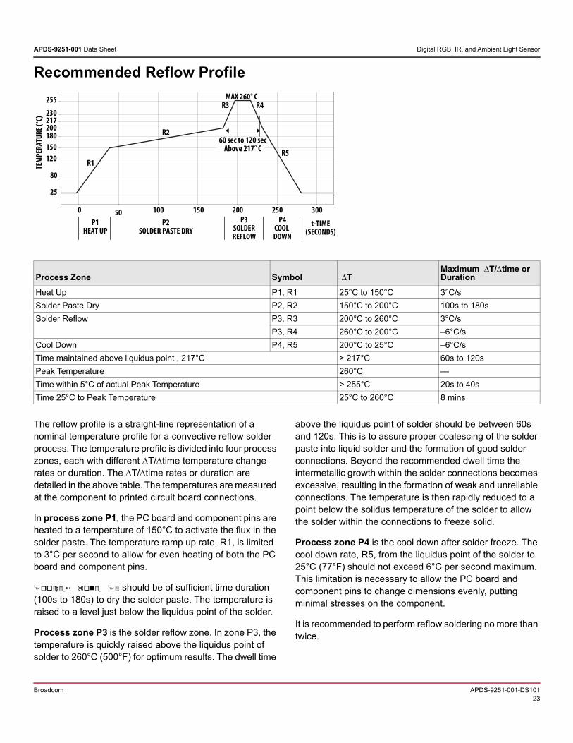
Recommended Reflow Profile
The reflow profile is a straight-line representation of a nominal temperature profile for a convective reflow solder process. The temperature profile is divided into four process zones, each with different T/time temperature change rates or duration. The T/time rates or duration are detailed in the above table. The temperatures are measured at the component to printed circuit board connections.
In process zone P1, the PC board and component pins are heated to a temperature of 150°C to activate the flux in the solder paste. The temperature ramp up rate, R1, is limited to 3°C per second to allow for even heating of both the PC board and component pins.
should be of sufficient time duration (100s to 180s) to dry the solder paste. The temperature is raised to a level just below the liquidus point of the solder.
Process zone P3 is the solder reflow zone. In zone P3, the temperature is quickly raised above the liquidus point of solder to 260°C (500°F) for optimum results. The dwell time
above the liquidus point of solder should be between 60s and 120s. This is to assure proper coalescing of the solder paste into liquid solder and the formation of good solder connections. Beyond the recommended dwell time the intermetallic growth within the solder connections becomes excessive, resulting in the formation of weak and unreliable connections. The temperature is then rapidly reduced to a point below the solidus temperature of the solder to allow the solder within the connections to freeze solid.
Process zone P4 is the cool down after solder freeze. The cool down rate, R5, from the liquidus point of the solder to 25°C (77°F) should not exceed 6°C per second maximum. This limitation is necessary to allow the PC board and component pins to change dimensions evenly, putting minimal stresses on the component.
It is recommended to perform reflow soldering no more than twice.
50 100 150 200 250 300
t-TIME(SECONDS)
25
80
120
150
180200
230
255
0
TEM
PER
ATU
RE
(°C)
R1
R2
R3 R4
R5
217
MAX 260° C
P1HEAT UP
P2SOLDER PASTE DRY
P3SOLDERREFLOW
P4COOL DOWN
60 sec to 120 secAbove 217° C
Process Zone Symbol TMaximum T/time or Duration
Heat Up P1, R1 25°C to 150°C 3°C/s
Solder Paste Dry P2, R2 150°C to 200°C 100s to 180s
Solder Reflow P3, R3 200°C to 260°C 3°C/s
P3, R4 260°C to 200°C –6°C/s
Cool Down P4, R5 200°C to 25°C –6°C/s
Time maintained above liquidus point , 217°C > 217°C 60s to 120s
Peak Temperature 260°C —
Time within 5°C of actual Peak Temperature > 255°C 20s to 40s
Time 25°C to Peak Temperature 25°C to 260°C 8 mins
Broadcom APDS-9251-001-DS10123

Broadcom, the pulse logo, Connecting everything, Avago Technologies, Avago, and the A logo are among the trademarks of Broadcom and/or its affiliates in the United States, certain other countries and/or the EU.
Copyright © 2018–2019 Broadcom. All Rights Reserved.
The term “Broadcom” refers to Broadcom Inc. and/or its subsidiaries. For more information, please visit www.broadcom.com.
Broadcom reserves the right to make changes without further notice to any products or data herein to improve reliability, function, or design. Information furnished by Broadcom is believed to be accurate and reliable. However, Broadcom does not assume any liability arising out of the application or use of this information, nor the application or use of any product or circuit described herein, neither does it convey any license under its patent rights nor the rights of others.
![Theoretical Analysis of InGaAs/InAlAs Single-Photon ......based APDs have high-electron mobility, leads to faster response times than that of InP-based APDs [16]. More-over, ionization](https://img.pdfslide.us/doc/110x75/60a9c8a12cb26c328b5f2fb4/theoretical-analysis-of-ingaasinalas-single-photon-based-apds-have-high-electron.jpg)

![[MS-APDS]: Authentication Protocol Domain Support · Security (TLS), and Digest authentication. APDS is used by NT LAN Manager (NTLM) and the APDS is used by NT LAN Manager (NTLM)](https://img.pdfslide.us/doc/110x75/5fe60c7971901a24cb29f5b7/ms-apds-authentication-protocol-domain-support-security-tls-and-digest-authentication.jpg)