Embed Size (px)
Citation preview
Chapter 8
Diffusion
Professor Paul K. Chu
City University of Hong Kong
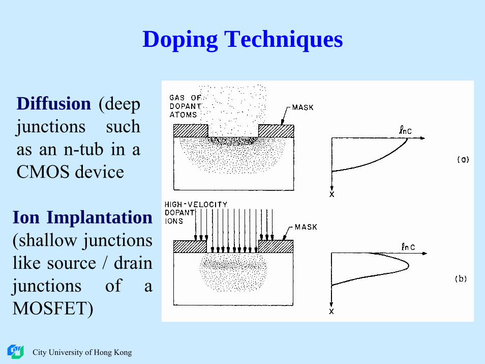
Doping Techniques
Diffusion (deep junctions such as an n-tub in a CMOS device
Ion Implantation(shallow junctions like source / drain junctions of a MOSFET)
City University of Hong Kong
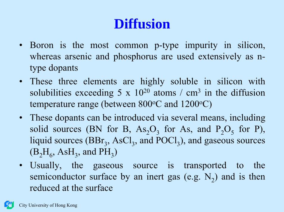
Diffusion• Boron is the most common p-type impurity in silicon,
whereas arsenic and phosphorus are used extensively as n-type dopants
• These three elements are highly soluble in silicon with solubilities exceeding 5 x 10²⁰ atoms / cm3 in the diffusion temperature range (between 800oC and 1200oC)
• These dopants can be introduced via several means, including solid sources (BN for B, As2O3 for As, and P2O5 for P), liquid sources (BBr3, AsCl3, and POCl3), and gaseous sources (B2H6, AsH3, and PH3)
• Usually, the gaseous source is transported to the semiconductor surface by an inert gas (e.g. N2) and is then reduced at the surface
City University of Hong Kong
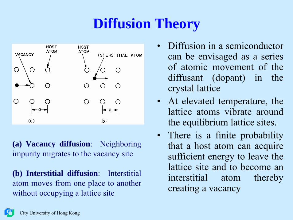
Diffusion Theory• Diffusion in a semiconductor
can be envisaged as a series of atomic movement of the diffusant (dopant) in the crystal lattice
• At elevated temperature, the lattice atoms vibrate around the equilibrium lattice sites.
• There is a finite probability that a host atom can acquire sufficient energy to leave the lattice site and to become an interstitial atom thereby creating a vacancy
(a) Vacancy diffusion: Neighboringimpurity migrates to the vacancy site
(b) Interstitial diffusion: Interstitial atom moves from one place to another without occupying a lattice site
City University of Hong Kong
The basic diffusion process of impurity atoms is similar to thatof charge carriers. F, the flux of dopant atoms traversing through a unit area in a unit time, is
xCDF∂∂
−=
where D is the diffusion coefficient, C is the dopantconcentration, and x is the distance in one dimension. The equation imparts that the main driving force of the diffusion process is the concentration gradient, .
xC∂∂
The flux is proportional to the concentration gradient, and the dopant atoms will diffuse from a high-concentration region toward a low-concentration region. The negative sign on the right-hand-side of the equation states that matters flow in the direction of decreasing dopant concentration, that is, the concentration gradient is negative.City University of Hong Kong
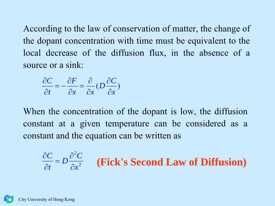
According to the law of conservation of matter, the change of the dopant concentration with time must be equivalent to the local decrease of the diffusion flux, in the absence of a source or a sink:
)(xCD
xxF
tC
∂∂
∂∂
=∂∂
−=∂∂
When the concentration of the dopant is low, the diffusion constant at a given temperature can be considered as a constant and the equation can be written as
2
2
xCD
tC
∂∂
=∂∂
(Fick's Second Law of Diffusion)
City University of Hong Kong
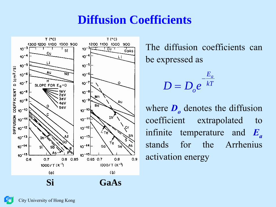
Diffusion Coefficients
The diffusion coefficients can be expressed as
where Do denotes the diffusion coefficient extrapolated to infinite temperature and Eastands for the Arrheniusactivation energy
kTE
o
a
eDD−
=
Si GaAs
City University of Hong Kong
• For interstitial diffusion, Ea is related to the energy required to move a dopant atom from one interstitial site to another
• The values of Ea are between 0.5 to 1.5 eV in both Si and GaAs
• For vacancy diffusion, Ea is related to both the energies of motion and formation of vacancies
• Ea for vacancy diffusion is larger than that for interstitial diffusion and is usually between 3 to 5 eV
• For fast diffusing species such as Cu, the measured activation energy is less than 2 eV, implying that interstitial atomic movement is the dominant diffusion mechanism
• For slow diffusing species like As, Ea is higher than 3 eV, and vacancy diffusion is naturally the dominant mechanism
City University of Hong Kong
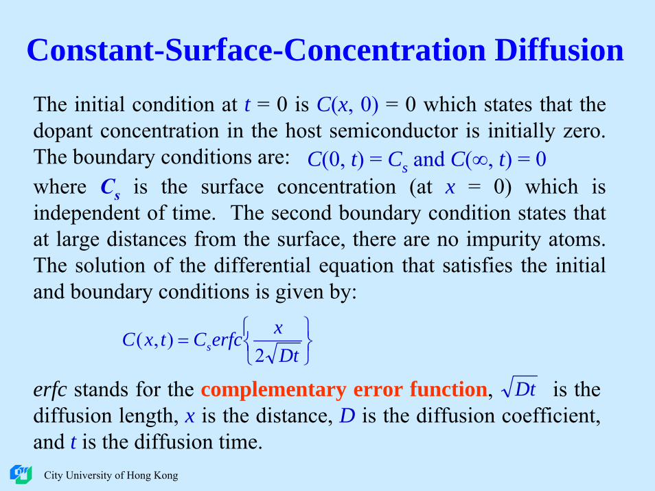
Constant-Surface-Concentration DiffusionThe initial condition at t = 0 is C(x, 0) = 0 which states that the dopant concentration in the host semiconductor is initially zero. The boundary conditions are: C(0, t) = Cs and C(∞, t) = 0where Cs is the surface concentration (at x = 0) which is independent of time. The second boundary condition states that at large distances from the surface, there are no impurity atoms. The solution of the differential equation that satisfies the initial and boundary conditions is given by:
⎭⎬⎫
⎩⎨⎧=
DtxerfcCtxC s 2
),(
erfc stands for the complementary error function, is the diffusion length, x is the distance, D is the diffusion coefficient, and t is the diffusion time.
Dt
City University of Hong Kong
Constant-Surface-Concentration Diffusion
• The total number of dopants per unit area of the semiconductor, Q(t), is given by integrating C(x, t)from x = 0 to x = ∞:
• The gradient of the diffusion, , can be obtained by differentiating:
DtCDtCtQ ss )13.1(2)( ≅=π
⎭⎬⎫
⎩⎨⎧−
−=Dtx
DtC
dxdC s
4exp
2
π
dxdC
City University of Hong Kong
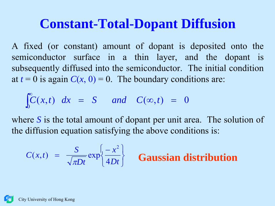
Constant-Total-Dopant DiffusionA fixed (or constant) amount of dopant is deposited onto the semiconductor surface in a thin layer, and the dopant is subsequently diffused into the semiconductor. The initial condition at t = 0 is again C(x, 0) = 0. The boundary conditions are:
0),(),(0
=∞=∫∞
tCandSdxtxC
where S is the total amount of dopant per unit area. The solution of the diffusion equation satisfying the above conditions is:
⎭⎬⎫
⎩⎨⎧−
=Dtx
DtStxC
4exp),(
2
π Gaussian distribution
City University of Hong Kong
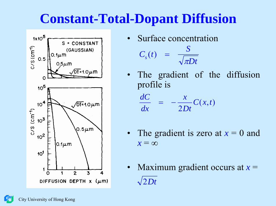
Constant-Total-Dopant Diffusion• Surface concentration
• The gradient of the diffusion profile is
• The gradient is zero at x = 0 and x = ∞
• Maximum gradient occurs at x =
DtStCs π
=)(
),(2
txCDtx
dxdC
−=
Dt2
City University of Hong Kong
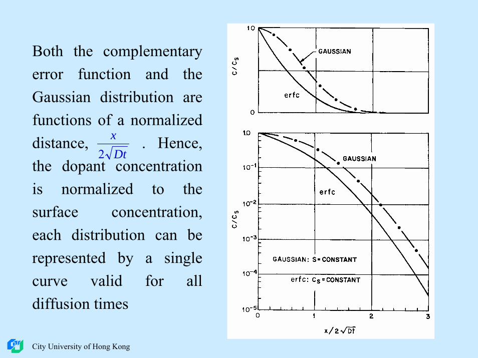
Both the complementary error function and the Gaussian distribution are functions of a normalized distance, . Hence, the dopant concentration is normalized to the surface concentration, each distribution can be represented by a single curve valid for all diffusion times
Dtx
2
City University of Hong Kong
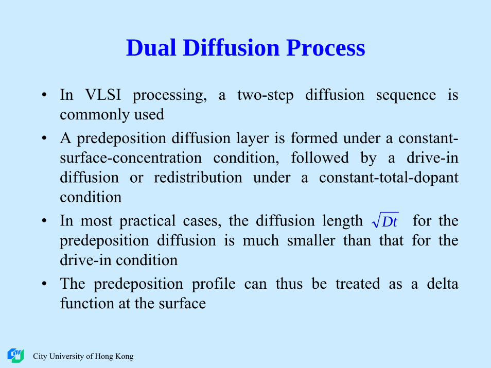
Dual Diffusion Process
• In VLSI processing, a two-step diffusion sequence is commonly used
• A predeposition diffusion layer is formed under a constant-surface-concentration condition, followed by a drive-in diffusion or redistribution under a constant-total-dopantcondition
• In most practical cases, the diffusion length for the predeposition diffusion is much smaller than that for the drive-in condition
• The predeposition profile can thus be treated as a delta function at the surface
Dt
City University of Hong Kong
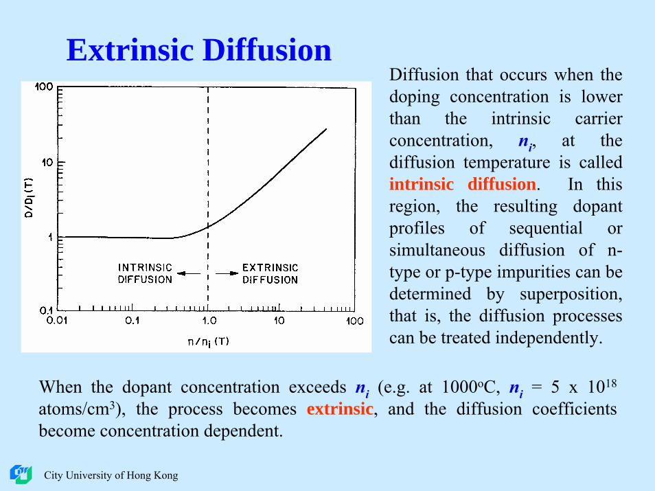
Extrinsic DiffusionDiffusion that occurs when the doping concentration is lower than the intrinsic carrier concentration, ni, at the diffusion temperature is called intrinsic diffusion. In this region, the resulting dopantprofiles of sequential or simultaneous diffusion of n-type or p-type impurities can be determined by superposition, that is, the diffusion processes can be treated independently.
When the dopant concentration exceeds ni (e.g. at 1000oC, ni = 5 x 10¹⁸
atoms/cm3), the process becomes extrinsic, and the diffusion coefficients become concentration dependent.
City University of Hong Kong
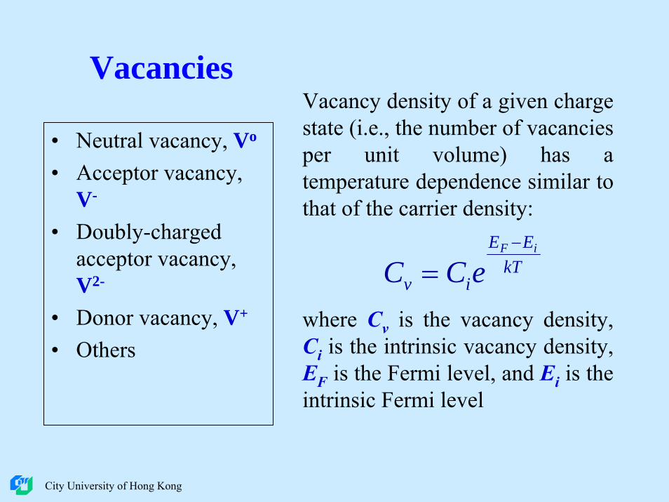
VacanciesVacancy density of a given charge state (i.e., the number of vacancies per unit volume) has a temperature dependence similar to that of the carrier density:
kTEE
iv
iF
eCC−
=
• Neutral vacancy, Vo
• Acceptor vacancy, V-
• Doubly-charged acceptor vacancy, V2-
• Donor vacancy, V+
• Otherswhere Cv is the vacancy density, Ci is the intrinsic vacancy density, EF is the Fermi level, and Ei is the intrinsic Fermi level
City University of Hong Kong
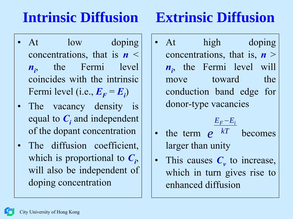
Intrinsic Diffusion Extrinsic Diffusion• At low doping
concentrations, that is n < ni, the Fermi level coincides with the intrinsic Fermi level (i.e., EF = Ei)
• The vacancy density is equal to Ci and independent of the dopant concentration
• The diffusion coefficient, which is proportional to Ci, will also be independent of doping concentration
• At high doping concentrations, that is, n > ni, the Fermi level will move toward the conduction band edge for donor-type vacancies
• the term becomes larger than unity
• This causes Cv to increase, which in turn gives rise to enhanced diffusion
kTEE iF
e−
City University of Hong Kong
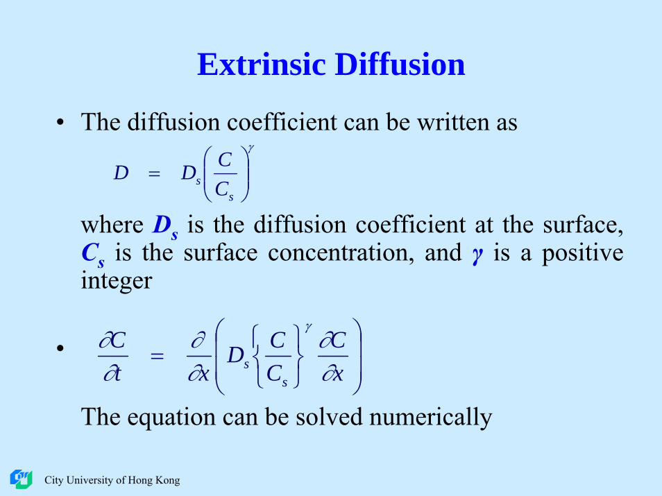
Extrinsic Diffusion
• The diffusion coefficient can be written as
where Ds is the diffusion coefficient at the surface, Cs is the surface concentration, and γ is a positive integer
•
The equation can be solved numerically
γ
⎟⎟⎠
⎞⎜⎜⎝
⎛=
ss C
CDD
⎟⎟
⎠
⎞
⎜⎜
⎝
⎛
⎭⎬⎫
⎩⎨⎧
=xC
CCD
xtC
ss ∂
∂∂∂
∂∂
γ
City University of Hong Kong
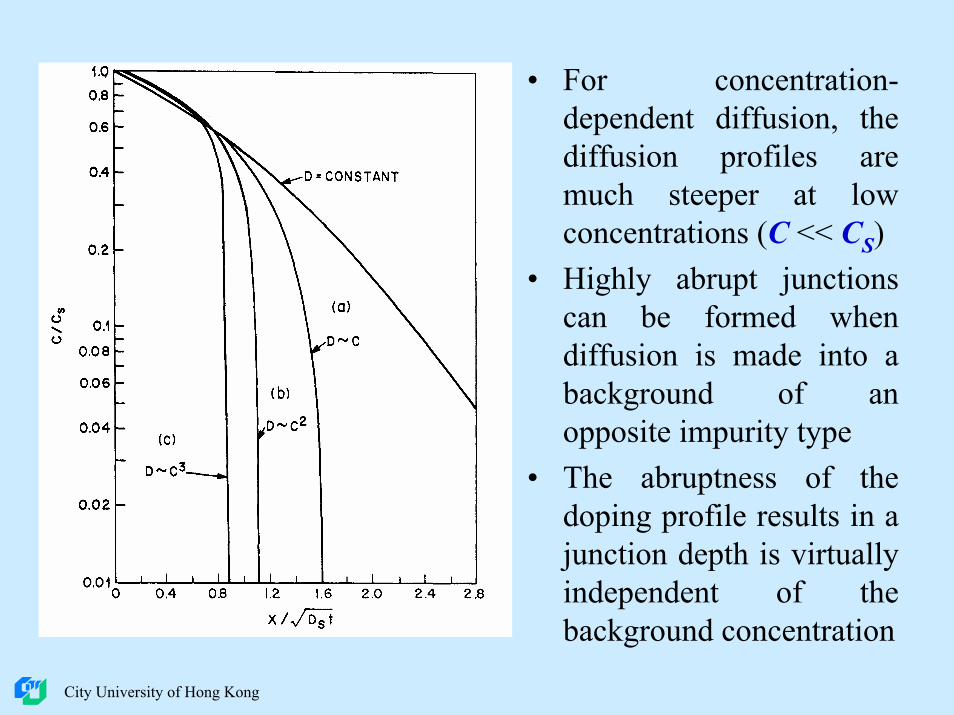
• For concentration-dependent diffusion, the diffusion profiles are much steeper at low concentrations (C << CS)
• Highly abrupt junctions can be formed when diffusion is made into a background of an opposite impurity type
• The abruptness of the doping profile results in a junction depth is virtually independent of the background concentration
City University of Hong Kong
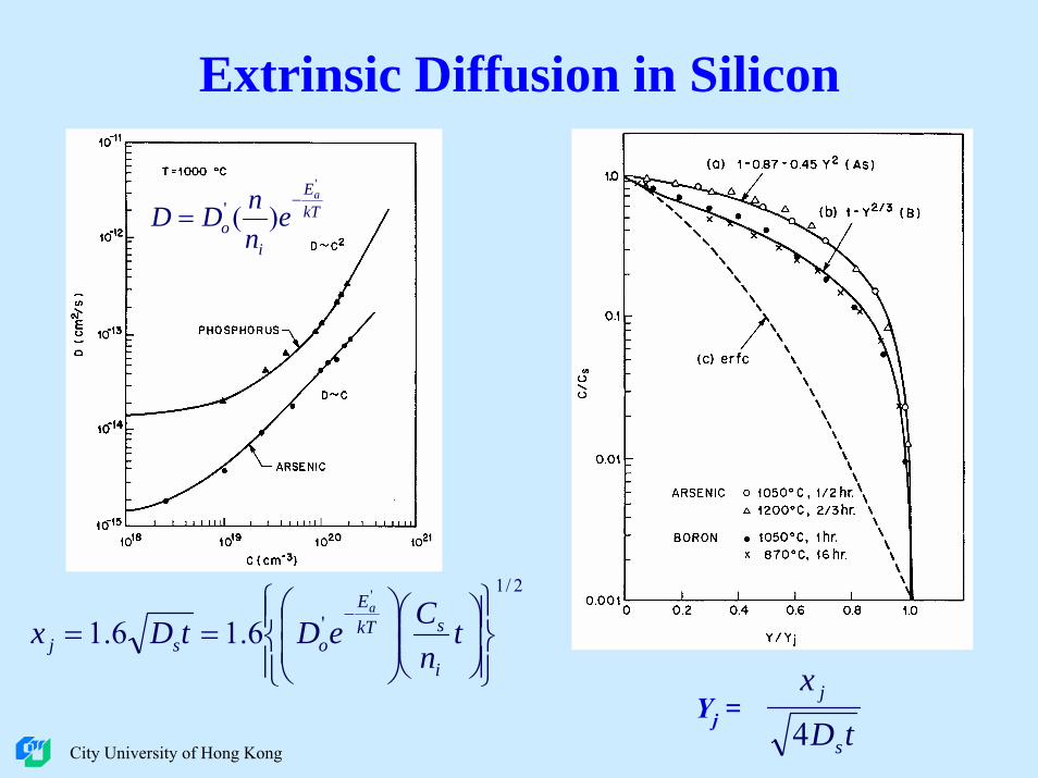
Extrinsic Diffusion in Silicon
Yj = tD
x
s
j
4
kTE
io
a
ennDD
'
)(' −=
2/1
''
6.16.1⎪⎭
⎪⎬⎫
⎪⎩
⎪⎨⎧
⎟⎟⎠
⎞⎜⎜⎝
⎛⎟⎟⎠
⎞⎜⎜⎝
⎛==
−t
nCeDtDx
i
skTE
osj
a
City University of Hong Kong
Phosphorus Diffusion in Silicon
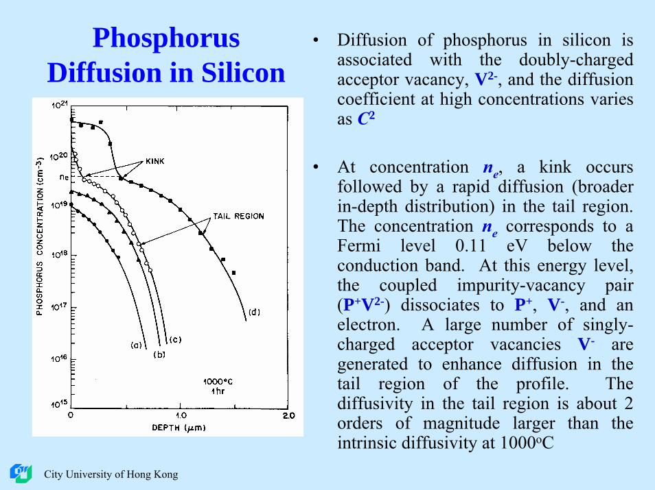
• Diffusion of phosphorus in silicon is associated with the doubly-charged acceptor vacancy, V2-, and the diffusion coefficient at high concentrations varies as C2
• At concentration ne, a kink occurs followed by a rapid diffusion (broader in-depth distribution) in the tail region. The concentration ne corresponds to a Fermi level 0.11 eV below the conduction band. At this energy level, the coupled impurity-vacancy pair (P+V2-) dissociates to P+, V-, and an electron. A large number of singly-charged acceptor vacancies V- are generated to enhance diffusion in the tail region of the profile. The diffusivity in the tail region is about 2 orders of magnitude larger than the intrinsic diffusivity at 1000oC
City University of Hong Kong
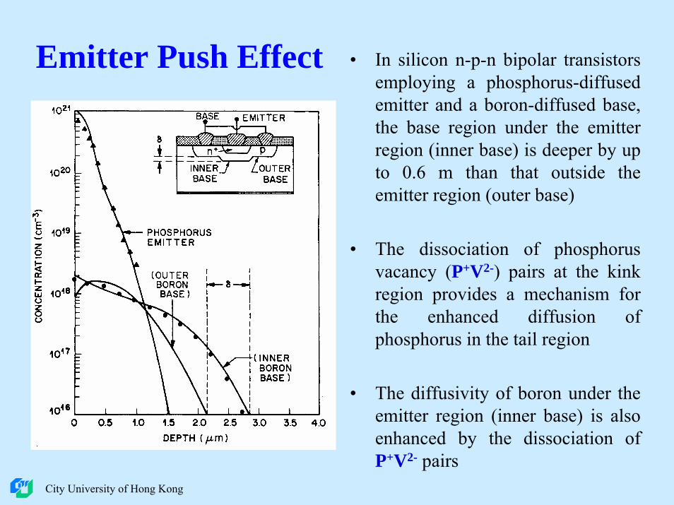
Emitter Push Effect • In silicon n-p-n bipolar transistors employing a phosphorus-diffused emitter and a boron-diffused base, the base region under the emitter region (inner base) is deeper by up to 0.6 m than that outside the emitter region (outer base)
• The dissociation of phosphorus vacancy (P+V2-) pairs at the kink region provides a mechanism for the enhanced diffusion of phosphorus in the tail region
• The diffusivity of boron under the emitter region (inner base) is also enhanced by the dissociation of P+V2- pairs
City University of Hong Kong
Diffusion Parameters
• Junction depth – Staining, Spreading Resistance Profiling (SRP), Secondary Ion Mass Spectrometry (SIMS), Capacitance –Voltage (C-V) Measurement
• Sheet resistance – Four-Point Probe• Dopant profile – SRP, SIMS, Differential
C-V Measurement
City University of Hong Kong
Staining• Junction depths are commonly measured on an angle-lapped
(1o to 5o) sample chemically stained by a mixture of 100 c.c. HF (49%) and a few drops of HNO3
• If the sample is subjected to strong illumination for one to twominutes, the p-type region will be stained darker than the n-type region, as a result of a reflectivity difference of the twoetched surfaces
• The location of the stained junction depends on the p-type concentration level and sometimes on the concentration gradient. In general, the stain boundary corresponds to a concentration level in the range of mid-1017 atoms/cm3
City University of Hong Kong
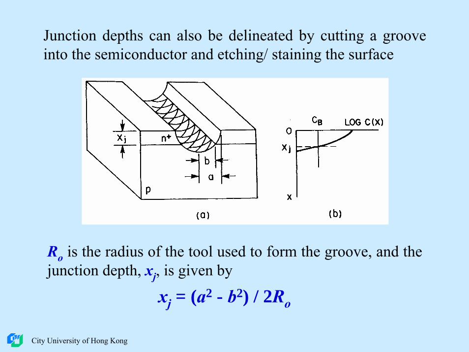
Junction depths can also be delineated by cutting a groove into the semiconductor and etching/ staining the surface
xj = (a2 - b2) / 2Ro
Ro is the radius of the tool used to form the groove, and the junction depth, xj, is given by
City University of Hong Kong
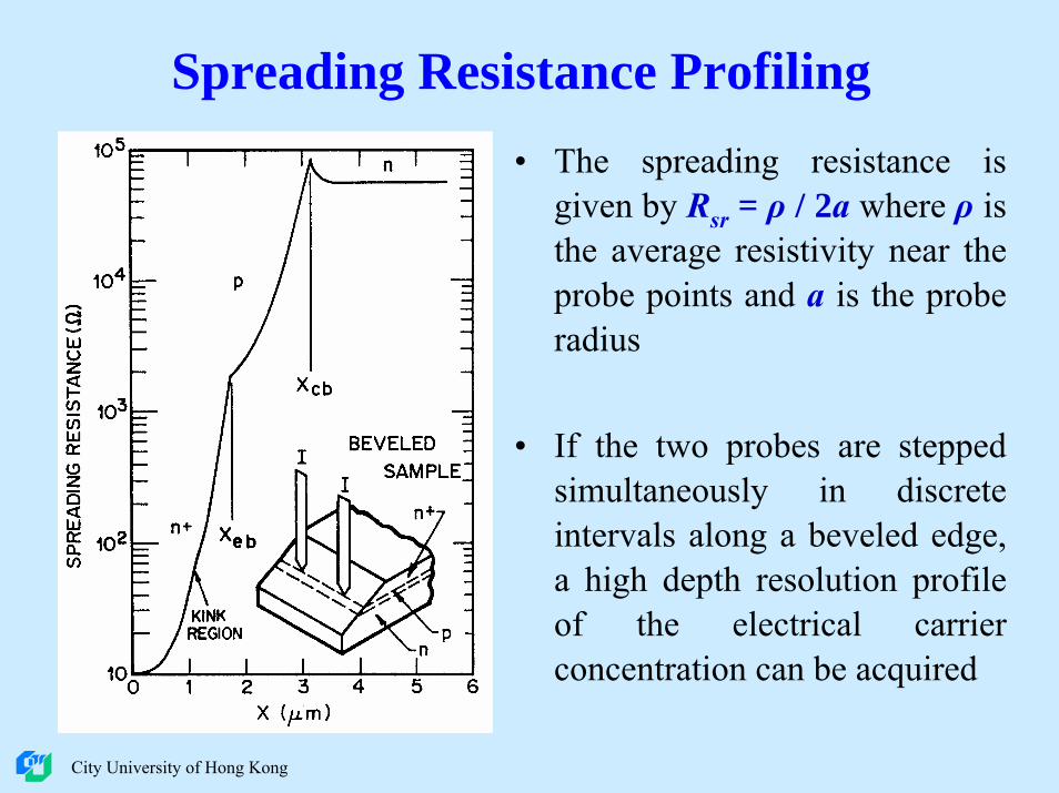
Spreading Resistance Profiling• The spreading resistance is
given by Rsr = ρ / 2a where ρ is the average resistivity near the probe points and a is the probe radius
• If the two probes are stepped simultaneously in discrete intervals along a beveled edge, a high depth resolution profile of the electrical carrier concentration can be acquired
City University of Hong Kong
Secondary Ion Mass Spectrometry
• Sputtering technique using typically an oxygen or cesium ion beam
• Excellent depth resolution (1 – 20 nm)• High sensitivity (“parts per million” to “parts per
billion” detection limits)• SIMS provides elemental (atomic) information
whereas electrical techniques such as SRP reveal electrical carrier concentration
• If a dopant is 100% activated (ionized), the SIMS and SRP results should theoretically agree
City University of Hong Kong
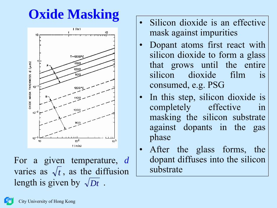
Oxide Masking• Silicon dioxide is an effective
mask against impurities• Dopant atoms first react with
silicon dioxide to form a glass that grows until the entire silicon dioxide film is consumed, e.g. PSG
• In this step, silicon dioxide is completely effective in masking the silicon substrate against dopants in the gas phase
• After the glass forms, the dopant diffuses into the silicon substrate
For a given temperature, dvaries as , as the diffusion length is given by .Dt
t
City University of Hong Kong
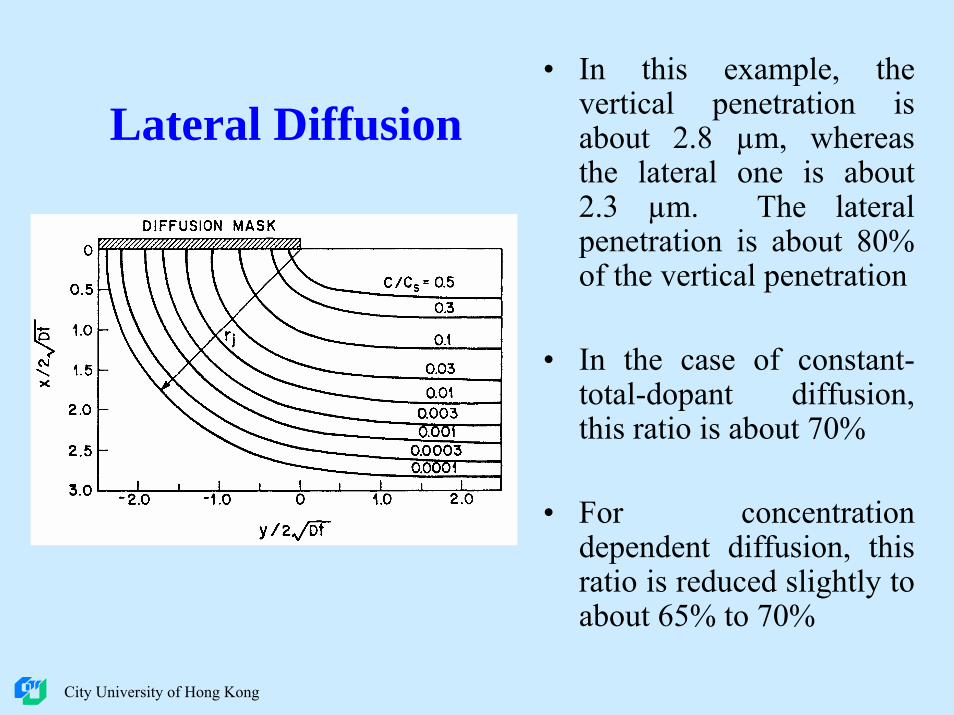
Lateral Diffusion• In this example, the
vertical penetration is about 2.8 µm, whereas the lateral one is about 2.3 µm. The lateral penetration is about 80% of the vertical penetration
• In the case of constant-total-dopant diffusion, this ratio is about 70%
• For concentration dependent diffusion, this ratio is reduced slightly to about 65% to 70%
City University of Hong Kong
Fast Diffusants
• Groups I and VII elements and some heavy metals like Au, Cu, Pt, are fast diffusants in silicon
• They are undesirable contaminants in VLSI and are usually gettered away from the active device regions by internal gettering techniques, that is, using SiOx clusters in the bulk of the wafer to trap impurities
City University of Hong Kong
Diffusion in Polysilicon
• Since the gate electrode is over a thin oxide (15 nm to 150 nm thick), dopant atoms in the polysilicon gate must be guarded against diffusing through the gate oxide
• Polysilicon films are usually deposited at a low temperature without doping elements
• After the gate region is defined, the polysiliconfilm is doped by diffusion (from a doped-oxide source or gas source) or by ion implantation
City University of Hong Kong
• Impurity diffusion in polysilicon film can be explained qualitatively by a grain-boundary model.
• The diffusivity of impurity atoms that migrate along grain boundaries can be up to 100 times larger than that in a single crystal lattice.
• Impurity atoms inside each crystallite have diffusivities eithercomparable to or a factor of 10 larger than those found in the single crystal
• The diffusivity in a polysilicon film depends strongly upon the structure (grain size, etc.) and texture that are in turn functions of the film deposition temperature, rate of deposition, thickness, and composition of the substrate
• It is difficult to predict diffusion profiles in polysilicon. Diffusivities are typically estimated from junction depths and surface concentrations are determined experimentally
City University of Hong Kong
![AP4120 Microelectronic Materials & Processing · 2017. 2. 6. · The effective density of states in the conduction band N C is equal to 2[2πm n kT/h 2]3/.Similarly, the effective](https://img.pdfslide.us/doc/110x75/60f7823ade6f2b209b6a0aa6/ap4120-microelectronic-materials-2017-2-6-the-effective-density-of-states.jpg)


![City University of Hong Kong › phy › appkchu › Patents › Chinese Patent... · CN 102341132 B [0001 ] 1/7 [0002] 19 61/153, 840 2009 2 E 20 61/154, 278 [0003] [0005] R. 0](https://img.pdfslide.us/doc/110x75/5f1e8965bb06fe16303e0549/city-university-of-hong-a-phy-a-appkchu-a-patents-a-chinese-patent.jpg)