Embed Size (px)
Citation preview
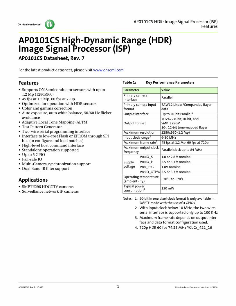
AP0101CS HDR: Image Signal Processor (ISP)Features
AP0101CS High-Dynamic Range (HDR) Image Signal Processor (ISP)AP0101CS Datasheet, Rev. 7
For the latest product datasheet, please visit www.onsemi.com
Features• Supports ON Semiconductor sensors with up to
1.2 Mp (1280x960)• 45 fps at 1.2 Mp, 60 fps at 720p • Optimized for operation with HDR sensors• Color and gamma correction• Auto exposure, auto white balance, 50/60 Hz flicker
avoidance• Adaptive Local Tone Mapping (ALTM)• Test Pattern Generator• Two-wire serial programming interface• Interface to low-cost Flash or EPROM through SPI
bus (to configure and load patches)• High-level host command interface• Standalone operation supported• Up to 5 GPIO• Fail-safe IO• Multi-Camera synchronization support• Dual Band IR filter support
Applications• SMPTE296 HDCCTV cameras• Surveillance network IP cameras
AP0101CS/D Rev. 7, 1/16 EN 1
Notes: 1. 20-bit in one pixel clock format is only available in SMPTE mode with the use of 4 GPIOs.
2. With input clock below 10 MHz, the two wire serial interface is supported only up to 100 KHz
3. Maximum frame rate depends on output inter-face and data format configuration used.
4. 720p HDR 60 fps 74.25 MHz YCbCr_422_16
Table 1: Key Performance Parameters
Parameter Value
Primary camera interface
Parallel
Primary camera input format
RAW12 Linear/Companded Bayer data
Output interface Up to 20-bit Parallel1
Output formatYUV422 8-bit,10-bit, and SMPTE296M10-, 12-bit tone-mapped Bayer
Maximum resolution 1280x960 (1.2 Mp)
Input clock range2 6-30 MHz
Maximum frame rate3 45 fps at 1.2 Mp, 60 fps at 720p
Maximum output clock frequency
Parallel clock up to 84 MHz
Supply voltage
VDDIO_S 1.8 or 2.8 V nominal
VDDIO_H 2.5 or 3.3 V nominal
VDD_REG 1.8V nominal
VDDIO_OTPM 2.5 or 3.3 V nominal
Operating temperature(ambient - TA)
–30°C to +70°C
Typical power consumption4 130 mW
©Semiconductor Components Industries, LLC 2016,
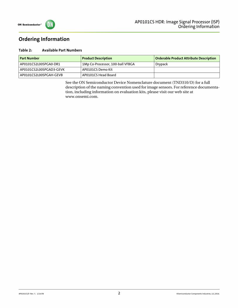
AP0101CS HDR: Image Signal Processor (ISP)Ordering Information
Ordering Information
See the ON Semiconductor Device Nomenclature document (TND310/D) for a full description of the naming convention used for image sensors. For reference documenta-tion, including information on evaluation kits, please visit our web site at www.onsemi.com.
Table 2: Available Part Numbers
Part Number Product Description Orderable Product Attribute Description
AP0101CS2L00SPGA0-DR1 1Mp Co-Processor, 100-ball VFBGA Drypack
AP0101CS2L00SPGAD3-GEVK AP0101CS Demo Kit
AP0101CS2L00SPGAH-GEVB AP0101CS Head Board
AP0101CS/D Rev. 7, 1/16 EN 2 ©Semiconductor Components Industries, LLC,2016.
AP0101CS/D Rev. 7, 1/16 EN 3 ©Semiconductor Components Industries, LLC,2016.
AP0101CS HDR: Image Signal Processor (ISP)Table of Contents
Table of Contents
Features . . . . . . . . . . . . . . . . . . . . . . . . . . . . . . . . . . . . . . . . . . . . . . . . . . . . . . . . . . . . . . . . . . . . . . . . . . . . . . . . . . . . . . . . . . . . . .1Applications . . . . . . . . . . . . . . . . . . . . . . . . . . . . . . . . . . . . . . . . . . . . . . . . . . . . . . . . . . . . . . . . . . . . . . . . . . . . . . . . . . . . . . . . . .1Ordering Information. . . . . . . . . . . . . . . . . . . . . . . . . . . . . . . . . . . . . . . . . . . . . . . . . . . . . . . . . . . . . . . . . . . . . . . . . . . . . . . . . .2General Description . . . . . . . . . . . . . . . . . . . . . . . . . . . . . . . . . . . . . . . . . . . . . . . . . . . . . . . . . . . . . . . . . . . . . . . . . . . . . . . . . . .4Functional Overview. . . . . . . . . . . . . . . . . . . . . . . . . . . . . . . . . . . . . . . . . . . . . . . . . . . . . . . . . . . . . . . . . . . . . . . . . . . . . . . . . . .4System Interfaces . . . . . . . . . . . . . . . . . . . . . . . . . . . . . . . . . . . . . . . . . . . . . . . . . . . . . . . . . . . . . . . . . . . . . . . . . . . . . . . . . . . . .4Multi-Camera Synchronization Support . . . . . . . . . . . . . . . . . . . . . . . . . . . . . . . . . . . . . . . . . . . . . . . . . . . . . . . . . . . . . . . .14Image Flow Processor. . . . . . . . . . . . . . . . . . . . . . . . . . . . . . . . . . . . . . . . . . . . . . . . . . . . . . . . . . . . . . . . . . . . . . . . . . . . . . . . .15Camera Control and Auto Functions . . . . . . . . . . . . . . . . . . . . . . . . . . . . . . . . . . . . . . . . . . . . . . . . . . . . . . . . . . . . . . . . . . .21AE Track Driver . . . . . . . . . . . . . . . . . . . . . . . . . . . . . . . . . . . . . . . . . . . . . . . . . . . . . . . . . . . . . . . . . . . . . . . . . . . . . . . . . . . . . .21Auto White Balance. . . . . . . . . . . . . . . . . . . . . . . . . . . . . . . . . . . . . . . . . . . . . . . . . . . . . . . . . . . . . . . . . . . . . . . . . . . . . . . . . . .22Dual Band IRCF . . . . . . . . . . . . . . . . . . . . . . . . . . . . . . . . . . . . . . . . . . . . . . . . . . . . . . . . . . . . . . . . . . . . . . . . . . . . . . . . . . . . . .22Exposure and White Balance Modes. . . . . . . . . . . . . . . . . . . . . . . . . . . . . . . . . . . . . . . . . . . . . . . . . . . . . . . . . . . . . . . . . . . .22Flicker Avoidance . . . . . . . . . . . . . . . . . . . . . . . . . . . . . . . . . . . . . . . . . . . . . . . . . . . . . . . . . . . . . . . . . . . . . . . . . . . . . . . . . . . .23Output Formatting . . . . . . . . . . . . . . . . . . . . . . . . . . . . . . . . . . . . . . . . . . . . . . . . . . . . . . . . . . . . . . . . . . . . . . . . . . . . . . . . . . .23Sensor Embedded Data . . . . . . . . . . . . . . . . . . . . . . . . . . . . . . . . . . . . . . . . . . . . . . . . . . . . . . . . . . . . . . . . . . . . . . . . . . . . . . .28Slave Two-Wire Serial Interface . . . . . . . . . . . . . . . . . . . . . . . . . . . . . . . . . . . . . . . . . . . . . . . . . . . . . . . . . . . . . . . . . . . . . . . .28Protocol . . . . . . . . . . . . . . . . . . . . . . . . . . . . . . . . . . . . . . . . . . . . . . . . . . . . . . . . . . . . . . . . . . . . . . . . . . . . . . . . . . . . . . . . . . . . .28Usage Modes . . . . . . . . . . . . . . . . . . . . . . . . . . . . . . . . . . . . . . . . . . . . . . . . . . . . . . . . . . . . . . . . . . . . . . . . . . . . . . . . . . . . . . . .33Host Command Interface . . . . . . . . . . . . . . . . . . . . . . . . . . . . . . . . . . . . . . . . . . . . . . . . . . . . . . . . . . . . . . . . . . . . . . . . . . . . .34Electrical Specifications. . . . . . . . . . . . . . . . . . . . . . . . . . . . . . . . . . . . . . . . . . . . . . . . . . . . . . . . . . . . . . . . . . . . . . . . . . . . . . .35Two-Wire Serial Register Interface . . . . . . . . . . . . . . . . . . . . . . . . . . . . . . . . . . . . . . . . . . . . . . . . . . . . . . . . . . . . . . . . . . . . .39Package and Die Options. . . . . . . . . . . . . . . . . . . . . . . . . . . . . . . . . . . . . . . . . . . . . . . . . . . . . . . . . . . . . . . . . . . . . . . . . . . . . .41
AP0101CS HDR: Image Signal Processor (ISP)General Description
General DescriptionThe ON Semiconductor AP0101CS is a high-performance, ultra-low power in-line, digital image processor optimized for use with High Dynamic Range (HDR) sensors. The AP0101CS provides full auto-functions support (AWB and AE) and Adaptive Local Tone Mapping (ALTM) to enhance HDR images and advanced noise reduction which enables excellent low-light performance.
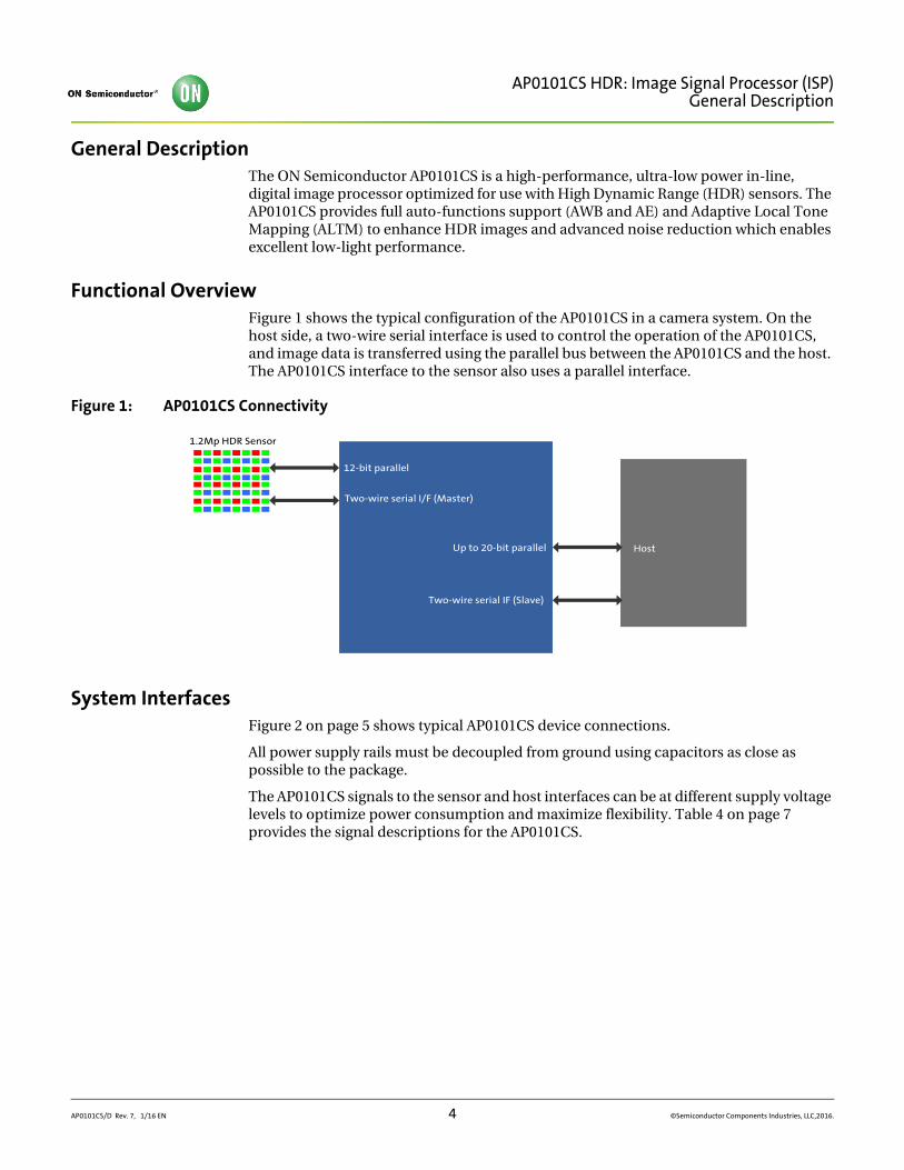
Functional OverviewFigure 1 shows the typical configuration of the AP0101CS in a camera system. On the host side, a two-wire serial interface is used to control the operation of the AP0101CS, and image data is transferred using the parallel bus between the AP0101CS and the host. The AP0101CS interface to the sensor also uses a parallel interface.
Figure 1: AP0101CS Connectivity
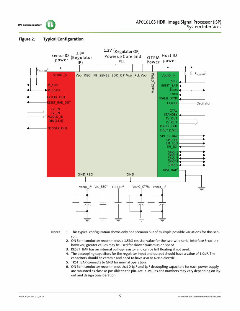
System InterfacesFigure 2 on page 5 shows typical AP0101CS device connections.
All power supply rails must be decoupled from ground using capacitors as close as possible to the package.
The AP0101CS signals to the sensor and host interfaces can be at different supply voltage levels to optimize power consumption and maximize flexibility. Table 4 on page 7 provides the signal descriptions for the AP0101CS.
1.2Mp HDR Sensor
12-bit parallel
HostUp to 20-bit parallel
Two-wire serial I/F (Master)
Two-wire serial IF (Slave)
AP0101CS/D Rev. 7, 1/16 EN 4 ©Semiconductor Components Industries, LLC,2016.
AP0101CS HDR: Image Signal Processor (ISP)System Interfaces
Figure 2: Typical Configuration
Notes: 1. This typical configuration shows only one scenario out of multiple possible variations for this sen-sor.
2. ON Semiconductor recommends a 1.5kresistor value for the two-wire serial interface RPULL-UP; however, greater values may be used for slower transmission speed.
3. RESET_BAR has an internal pull-up resistor and can be left floating if not used.4. The decoupling capacitors for the regulator input and output should have a value of 1.0uF. The
capacitors should be ceramic and need to have X5R or X7R dielectric.5. TRST_BAR connects to GND for normal operation.6. ON Semiconductor recommends that 0.1F and 1F decoupling capacitors for each power supply
are mounted as close as possible to the pin. Actual values and numbers may vary depending on lay-out and design consideration
VDDIO_OTPMLDO_OP4VDD_REG4VDDIO_S6
VDDIO _S VDDIO _H
S ensor IO pow er
H ost IO pow er
M_SCLK
M_SDATA
EXTCLK_OUT
RESET_BAR_OUT
FV_INLV_IN
PIXCLK _INDIN [11:0]
TRIGGER_OUT
VDD _REG FB _SENSE LDO_O P VDD _PLL
1.8V (R egulator
IP )
VDD
1.2V (R egulator OP)P ower up C ore and
P LL
G ND_REG
FV_OUTLV_OUT
PIXCLK_OUTDOUT [15:0]
SCLK
SDATA
SADDR
EXTCLK
XTAL
SPI_CS_BARSPI_CLKSPI_SDOSPI_SDI
GPIO_1
TRST_BAR5
VD
DIO
_O
TPM
O T P M P ow er
VDDIO_H6
G ND
RPULL-UP2
RPULL-UP2
RESET_BAR3
GPIO_2GPIO_3GPIO_4GPIO_5
FRAME_SYNC
STANDBY
Oscillator
AP0101CS/D Rev. 7, 1/16 EN 5 ©Semiconductor Components Industries, LLC,2016.
AP0101CS HDR: Image Signal Processor (ISP)System Interfaces
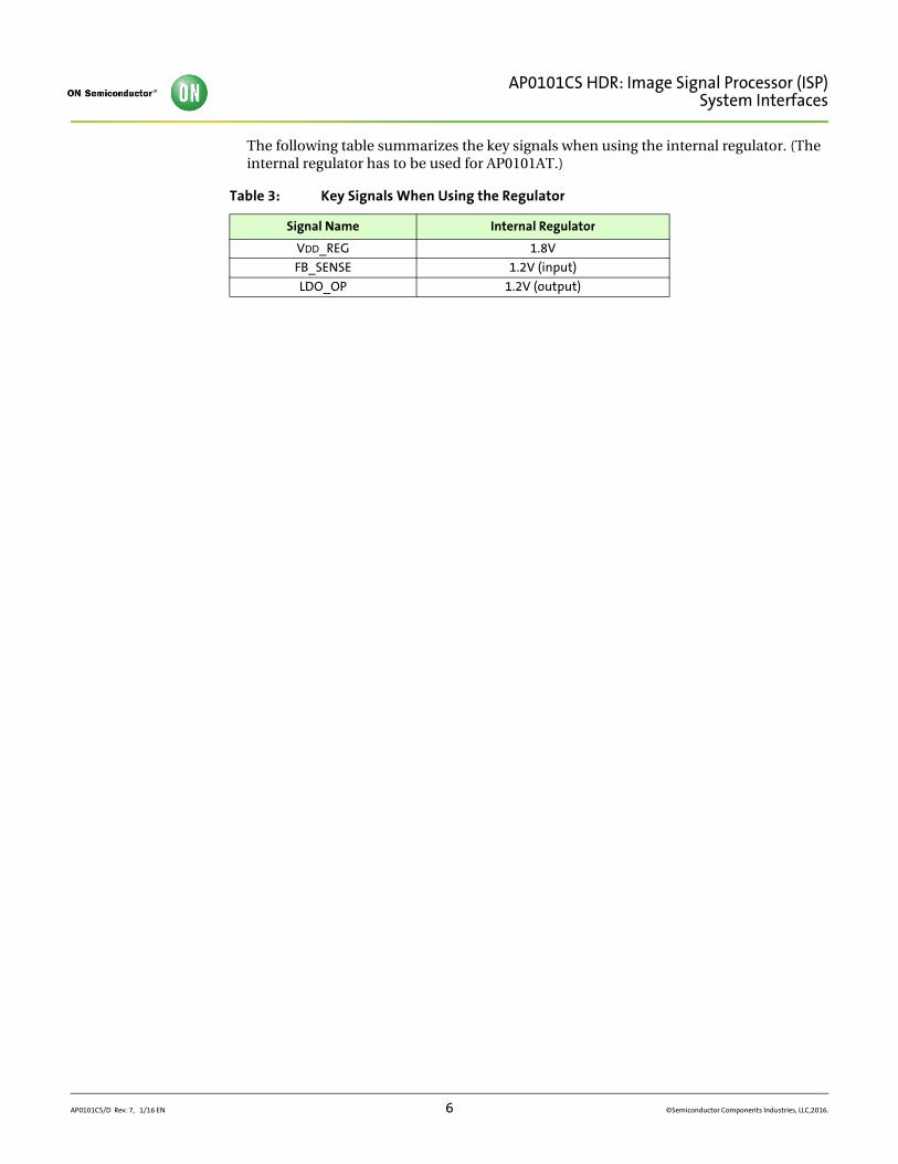
The following table summarizes the key signals when using the internal regulator. (The internal regulator has to be used for AP0101AT.)
Table 3: Key Signals When Using the Regulator
Signal Name Internal Regulator
VDD_REG 1.8V
FB_SENSE 1.2V (input)
LDO_OP 1.2V (output)
AP0101CS/D Rev. 7, 1/16 EN 6 ©Semiconductor Components Industries, LLC,2016.
AP0101CS HDR: Image Signal Processor (ISP)System Interfaces
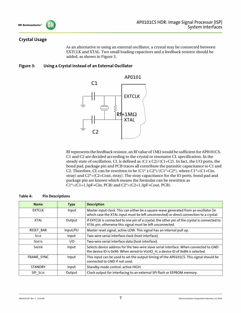
Crystal Usage
As an alternative to using an external oscillator, a crystal may be connected between EXTCLK and XTAL. Two small loading capacitors and a feedback resistor should be added, as shown in Figure 3.
Figure 3: Using a Crystal Instead of an External Oscillator
Rf represents the feedback resistor, an Rf value of 1M would be sufficient for AP0101CS. C1 and C2 are decided according to the crystal or resonator CL specification. In the steady state of oscillation, CL is defined as (C1 x C2)/(C1+C2). In fact, the I/O ports, the bond pad, package pin and PCB traces all contribute the parasitic capacitance to C1 and C2. Therefore, CL can be rewritten to be (C1* x C2*)/(C1*+C2*), where C1*=(C1+Cin, stray) and C2*=(C2+Cout, stray). The stray capacitance for the IO ports, bond pad and package pin are known which means the formulas can be rewritten as C1*=(C1+1.5pF+Cin, PCB) and C2*=(C2+1.3pF+Cout, PCB).
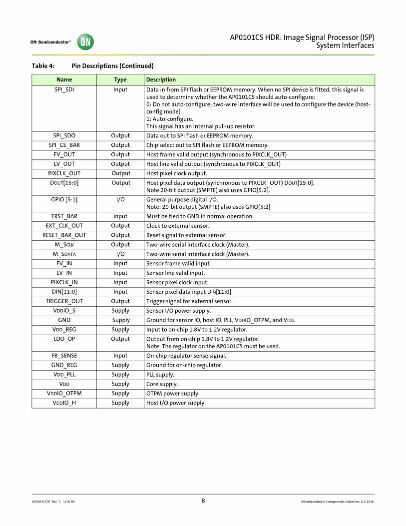
Table 4: Pin Descriptions
Name Type Description
EXTCLK Input Master input clock. This can either be a square-wave generated from an oscillator (in which case the XTAL input must be left unconnected) or direct connection to a crystal.
XTAL Output If EXTCLK is connected to one pin of a crystal, the other pin of the crystal is connected to XTAL pin; otherwise this signal must be left unconnected.
RESET_BAR Input/PU Master reset signal, active LOW. This signal has an internal pull up.
SCLK Input Two-wire serial interface clock (host interface).
SDATA I/O Two-wire serial interface data (host interface).
SADDR Input Selects device address for the two-wire slave serial interface. When connected to GND the device ID is 0x90. When wired to VDDIO_H, a device ID of 0xBA is selected.
FRAME_SYNC Input This input can be used to set the output timing of the AP0101CS. This signal should be connected to GND if not used.
STANDBY Input Standby mode control, active HIGH.
SPI_SCLK Output Clock output for interfacing to an external SPI flash or EEPROM memory.
EXTCLK
XTAL
AP0101C1
C2
Rf=1MΩ
AP0101CS/D Rev. 7, 1/16 EN 7 ©Semiconductor Components Industries, LLC,2016.
AP0101CS HDR: Image Signal Processor (ISP)System Interfaces
SPI_SDI Input Data in from SPI flash or EEPROM memory. When no SPI device is fitted, this signal is used to determine whether the AP0101CS should auto-configure:0: Do not auto-configure; two-wire interface will be used to configure the device (host-config mode)1: Auto-configure.This signal has an internal pull-up resistor.
SPI_SDO Output Data out to SPI flash or EEPROM memory.
SPI_CS_BAR Output Chip select out to SPI flash or EEPROM memory.
FV_OUT Output Host frame valid output (synchronous to PIXCLK_OUT)
LV_OUT Output Host line valid output (synchronous to PIXCLK_OUT)
PIXCLK_OUT Output Host pixel clock output.
DOUT[15:0] Output Host pixel data output (synchronous to PIXCLK_OUT) DOUT[15:0].Note 20-bit output (SMPTE) also uses GPIO[5:2].
GPIO [5:1] I/O General purpose digital I/O. Note: 20-bit output (SMPTE) also uses GPIO[5:2]
TRST_BAR Input Must be tied to GND in normal operation.
EXT_CLK_OUT Output Clock to external sensor.
RESET_BAR_OUT Output Reset signal to external sensor.
M_SCLK Output Two-wire serial interface clock (Master).
M_SDATA I/O Two-wire serial interface clock (Master).
FV_IN Input Sensor frame valid input.
LV_IN Input Sensor line valid input.
PIXCLK_IN Input Sensor pixel clock input.
DIN[11:0] Input Sensor pixel data input DIN[11:0]
TRIGGER_OUT Output Trigger signal for external sensor.
VDDIO_S Supply Sensor I/O power supply.
GND Supply Ground for sensor IO, host IO, PLL, VDDIO_OTPM, and VDD.
VDD_REG Supply Input to on-chip 1.8V to 1.2V regulator.
LDO_OP Output Output from on-chip 1.8V to 1.2V regulator.Note: The regulator on the AP0101CS must be used.
FB_SENSE Input On-chip regulator sense signal.
GND_REG Supply Ground for on-chip regulator
VDD_PLL Supply PLL supply.
VDD Supply Core supply.
VDDIO_OTPM Supply OTPM power supply.
VDDIO_H Supply Host I/O power supply.
Table 4: Pin Descriptions (Continued)
Name Type Description
AP0101CS/D Rev. 7, 1/16 EN 8 ©Semiconductor Components Industries, LLC,2016.
AP0101CS HDR: Image Signal Processor (ISP)System Interfaces
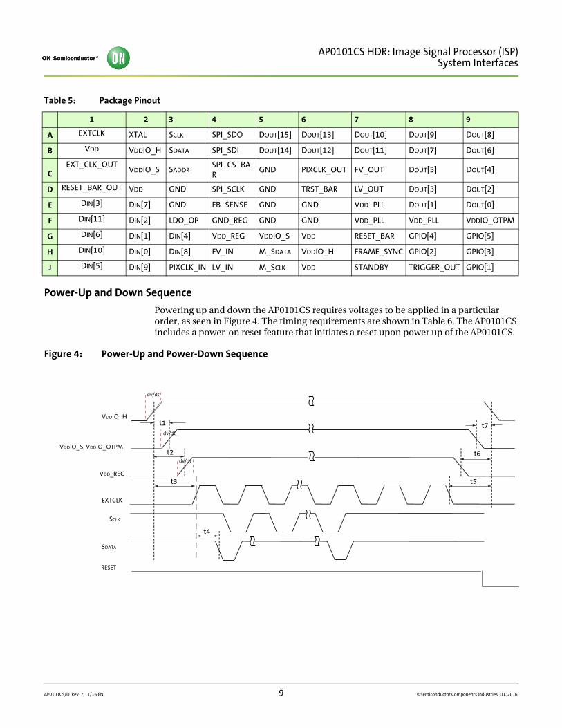
Power-Up and Down Sequence
Powering up and down the AP0101CS requires voltages to be applied in a particular order, as seen in Figure 4. The timing requirements are shown in Table 6. The AP0101CS includes a power-on reset feature that initiates a reset upon power up of the AP0101CS.
Figure 4: Power-Up and Power-Down Sequence
Table 5: Package Pinout
1 2 3 4 5 6 7 8 9
A EXTCLK XTAL SCLK SPI_SDO DOUT[15] DOUT[13] DOUT[10] DOUT[9] DOUT[8]
B VDD VDDIO_H SDATA SPI_SDI DOUT[14] DOUT[12] DOUT[11] DOUT[7] DOUT[6]
C EXT_CLK_OUT
VDDIO_S SADDRSPI_CS_BAR
GND PIXCLK_OUT FV_OUT DOUT[5] DOUT[4]
D RESET_BAR_OUT VDD GND SPI_SCLK GND TRST_BAR LV_OUT DOUT[3] DOUT[2]
E DIN[3] DIN[7] GND FB_SENSE GND GND VDD_PLL DOUT[1] DOUT[0]
F DIN[11] DIN[2] LDO_OP GND_REG GND GND VDD_PLL VDD_PLL VDDIO_OTPM
G DIN[6] DIN[1] DIN[4] VDD_REG VDDIO_S VDD RESET_BAR GPIO[4] GPIO[5]
H DIN[10] DIN[0] DIN[8] FV_IN M_SDATA VDDIO_H FRAME_SYNC GPIO[2] GPIO[3]
J DIN[5] DIN[9] PIXCLK_IN LV_IN M_SCLK VDD STANDBY TRIGGER_OUT GPIO[1]
VDDIO_H
VDD_REGt3 t5
EXTCLK
SCLK
t4
SDATA
t1
t2
t7
t6VDDIO_S, VDDIO_OTPM
dv/dt
dv/dt
dv/dt
RESET
AP0101CS/D Rev. 7, 1/16 EN 9 ©Semiconductor Components Industries, LLC,2016.
AP0101CS HDR: Image Signal Processor (ISP)System Interfaces
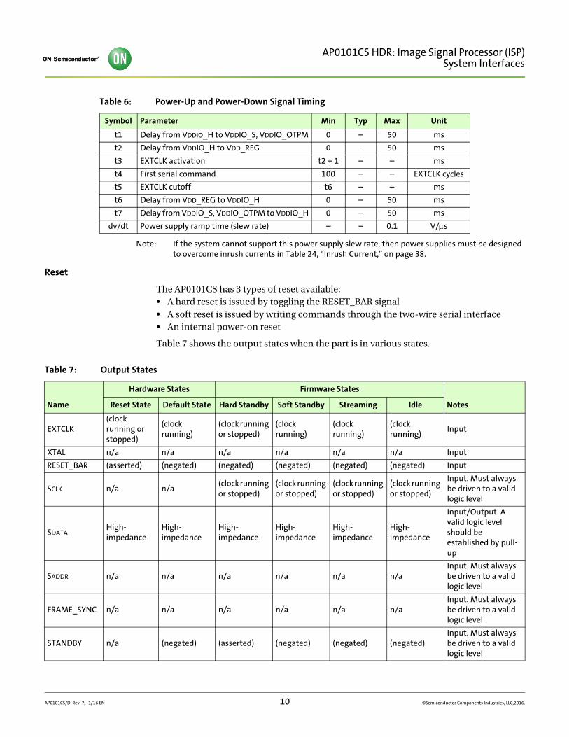
Note: If the system cannot support this power supply slew rate, then power supplies must be designed to overcome inrush currents in Table 24, “Inrush Current,” on page 38.
Reset
The AP0101CS has 3 types of reset available:• A hard reset is issued by toggling the RESET_BAR signal• A soft reset is issued by writing commands through the two-wire serial interface• An internal power-on reset
Table 7 shows the output states when the part is in various states.
Table 6: Power-Up and Power-Down Signal Timing
Symbol Parameter Min Typ Max Unit
t1 Delay from VDDIO_H to VDDIO_S, VDDIO_OTPM 0 – 50 ms
t2 Delay from VDDIO_H to VDD_REG 0 – 50 ms
t3 EXTCLK activation t2 + 1 – – ms
t4 First serial command 100 – – EXTCLK cycles
t5 EXTCLK cutoff t6 – – ms
t6 Delay from VDD_REG to VDDIO_H 0 – 50 ms
t7 Delay from VDDIO_S, VDDIO_OTPM to VDDIO_H 0 – 50 ms
dv/dt Power supply ramp time (slew rate) – – 0.1 V/s
Table 7: Output States
Name
Hardware States Firmware States
NotesReset State Default State Hard Standby Soft Standby Streaming Idle
EXTCLK(clock running or stopped)
(clock running)
(clock running or stopped)
(clock running)
(clock running)
(clock running)
Input
XTAL n/a n/a n/a n/a n/a n/a Input
RESET_BAR (asserted) (negated) (negated) (negated) (negated) (negated) Input
SCLK n/a n/a(clock running or stopped)
(clock running or stopped)
(clock running or stopped)
(clock running or stopped)
Input. Must always be driven to a valid logic level
SDATAHigh-impedance
High-impedance
High-impedance
High-impedance
High-impedance
High-impedance
Input/Output. A valid logic level should be established by pull-up
SADDR n/a n/a n/a n/a n/a n/aInput. Must always be driven to a valid logic level
FRAME_SYNC n/a n/a n/a n/a n/a n/aInput. Must always be driven to a valid logic level
STANDBY n/a (negated) (asserted) (negated) (negated) (negated)Input. Must always be driven to a valid logic level
AP0101CS/D Rev. 7, 1/16 EN 10 ©Semiconductor Components Industries, LLC,2016.
AP0101CS HDR: Image Signal Processor (ISP)System Interfaces
SPI_SCLKHigh-impedance
driven, logic 0 driven, logic 0 driven, logic 0 Output
SPI_SDIInternal pull-up enabled
Internal pull-up enabled
Internal pull-up enabled
internal pull-up enabled
Input. Internal pull-up permanently enabled.
SPI_SDOHigh-impedance
driven, logic 0 driven, logic 0 driven, logic 0 Output
SPI_CS_BARHigh-impedance
driven, logic 1 driven, logic 1 driven, logic 1 Output
EXT_CLK_OUTdriven, logic 0
driven, logic 0 driven, logic 0 driven, logic 0 Output
RESET_BAR_OUT
driven, logic 0
driven, logic 0 driven, logic 1 driven, logic 1Output. Firmware will release sensor reset
M_SCLKHigh-impedance
High-impedance
High-impedance
High-impedance
Input/Output. A valid logic level should be established by pull-up
M_SDATAHigh-impedance
High-impedance
High-impedance
High-impedance
Input/Output. A valid logic level should be established by pull-up
FV_IN ,LV_IN, PIXCLK_IN, DIN[11:0]
n/a n/a n/a n/a n/aInput. Must always be driven to a valid logic level
FV_OUT, LV_OUT, PIXCLK_OUT, DOUT[15:0]
High-impedance
Varied Driven if used Driven if used Driven if used Driven if usedOutput. Default state dependent on configuration
GPIO[5:2]High-impedance
Input, then high-impedance
Driven if used Driven if used Driven if used Driven if used
Input/Output. After reset these pins are sampled as inputs as part of auto-configuration.
GPIO1 High-impedance
High-impedance
High-impedance
High-impedance
High-impedance
High-impedance
TRIGGER_OUTHigh-impedance
High-impedance
Driven if used Driven if used Driven if used Driven if used
TRST_BAR n/a n/a (negated) (negated) (negated) (negated)Input. Must always be driven to a valid logic level.
Table 7: Output States
Name
Hardware States Firmware States
NotesReset State Default State Hard Standby Soft Standby Streaming Idle
AP0101CS/D Rev. 7, 1/16 EN 11 ©Semiconductor Components Industries, LLC,2016.
AP0101CS HDR: Image Signal Processor (ISP)System Interfaces
Hard Reset
The AP0101CS enters the reset state when the external RESET_BAR signal is asserted LOW, as shown in Figure 5. All the output signals will be in High-Z state.
Figure 5: Hard Reset Operation
Note: This assumes auto-config.
Soft Reset
A soft reset sequence to the AP0101CS can be activated by writing to a register through the two-wire serial interface.
Hard Standby Mode
The AP0101CS can enter hard standby mode by using the external STANDBY signal, as shown in Figure 6.
Entering Standby Mode
1. Assert STANDBY signal HIGH.
Exiting Standby Mode
1. De-assert STANDBY signal LOW.
Table 8: Hard Reset
Symbol Definition Min Typ Max Unit
t1 RESET_BAR pulse width 50 – –EXTCLK cycles
t2 Active EXTCLK required after RESET_BAR asserted 10 – –
t3 Active EXTCLK required before RESET_BAR de-asserted
10 – –
t4 First two-wire serial interface communication after RESET_BAR is HIGH
100 – –
EXTCLK
Reset
RESET_BAR
Mode
t2
t3
t1
Internal Initialization Time
SDATA
Enter streaming mode
t4
All Outputs
Data Active Data Active
AP0101CS/D Rev. 7, 1/16 EN 12 ©Semiconductor Components Industries, LLC,2016.
AP0101CS HDR: Image Signal Processor (ISP)System Interfaces
Figure 6: Hard Standby Operation
Table 9: Hard Standby Signal Timing
Symbol Parameter Min Typ Max Unitt1 Standby entry complete – – 2 Frames Linest2 Active EXTCLK required after going into STANDBY
mode10 – – EXTCLKs
t3 Active EXTCLK required before STANDBYde-asserted
10 – – EXTCLKs
EXTCLK
STANDBY
STANDBY Asserted
t1
STANDBYMode EXTCLK Disabled
t2 t3
EXTCLK EnabledMode
AP0101CS/D Rev. 7, 1/16 EN 13 ©Semiconductor Components Industries, LLC,2016.
AP0101CS HDR: Image Signal Processor (ISP)Multi-Camera Synchronization Support
Multi-Camera Synchronization SupportThe AP0101CS supports multi-camera synchronization via the FRAME_SYNC pin. The host (or controlling entity) 'broadcasts' a sync-pulse to all cameras within the system that triggers streaming start. The AP0101CS will propagate the signal to the TRIG-GER_OUT pin to the sensor's TRIGGER pin.
The AP0101CSsupports two different trigger modes. The first mode supported is 'single-shot'; this is when the trigger pulse will cause one frame to be output from the image sensor and AP0101CS (see Figure 7).
Figure 7: Single-Shot Mode
Table 10: Trigger Timing
Parameter Name Conditions Min Typ Max Unit
FRAME_SYNC to FV_OUT tFRMSYNC_FVH 8 lines+ exposure time + sensor delay
– – Lines
FRAME_SYNC to TRIGGER_OUT
tTRIGGER_PROP – – 9 ns
tFRAME_SYNC tFRAMESYNC 3 – – EXTCLK cycles
AP0101CS/D Rev. 7, 1/16 EN 14 ©Semiconductor Components Industries, LLC,2016.
AP0101CS HDR: Image Signal Processor (ISP)Image Flow Processor
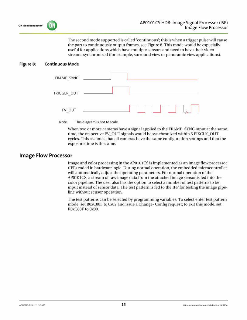
The second mode supported is called 'continuous'; this is when a trigger pulse will cause the part to continuously output frames, see Figure 8. This mode would be especially useful for applications which have multiple sensors and need to have their video streams synchronized (for example, surround view or panoramic view applications).
Figure 8: Continuous Mode
Note: This diagram is not to scale.
When two or more cameras have a signal applied to the FRAME_SYNC input at the same time, the respective FV_OUT signals would be synchronized within 5 PIXCLK_OUT cycles. This assumes that all cameras have the same configuration settings and that the exposure time is the same.
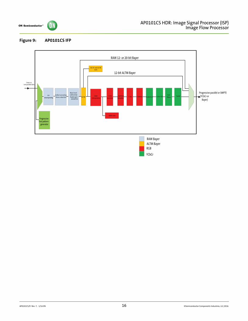
Image Flow ProcessorImage and color processing in the AP0101CS is implemented as an image flow processor (IFP) coded in hardware logic. During normal operation, the embedded microcontroller will automatically adjust the operating parameters. For normal operation of the AP0101CS, a stream of raw image data from the attached image sensor is fed into the color pipeline. The user also has the option to select a number of test patterns to be input instead of sensor data. The test pattern is fed to the IFP for testing the image pipe-line without sensor operation.
The test patterns can be selected by programming variables. To select enter test pattern mode, set R0xC88F to 0x02 and issue a Change- Config request; to exit this mode, set R0xC88F to 0x00.
FRAME_SYNC
TRIGGER_OUT
FV_OUT
AP0101CS/D Rev. 7, 1/16 EN 15 ©Semiconductor Components Industries, LLC,2016.
AP0101CS HDR: Image Signal Processor (ISP)Image Flow Processor
Figure 9: AP0101CS IFP
linear or com panded data
D efect correction, N oise reduction
R X decompanding
Black level subtraction,D igital gain
control PGA,
RAW 12- or 20-bit Bayer
AE, F D and ALT M stats
12-bit ALTM Bayer
C olor Interpolation
ALT MC olor
CorrectionAperture
CorrectionGamma R G B 2YU V
AW B stats
C olor KillYU V
filtersScalerC rop
ProgressiveTest pattern
generator
RAW BayerALTM BayerRGB
YCbCr
Progressive parallel or SMPTE(YCbCr or
Bayer)
AP0101CS/D Rev. 7, 1/16 EN 16 ©Semiconductor Components Industries, LLC,2016.
AP0101CS HDR: Image Signal Processor (ISP)Image Flow Processor
Test Patterns
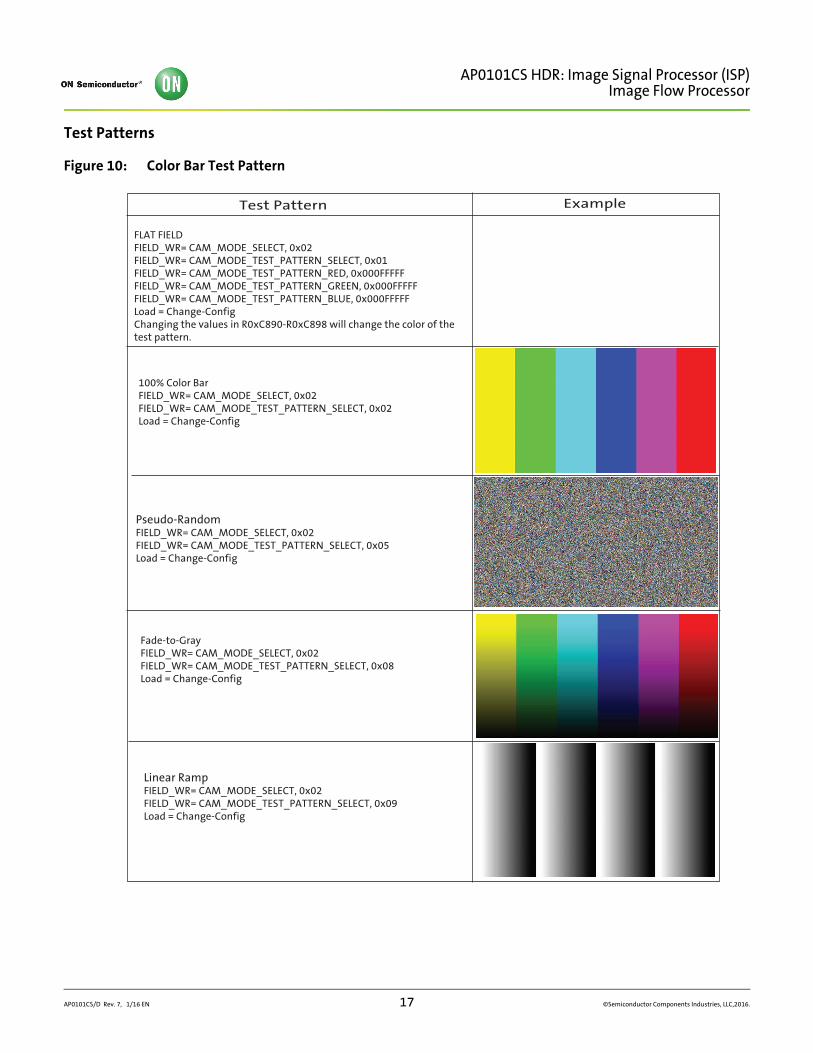
Figure 10: Color Bar Test Pattern
Test Pattern Example
FLAT FIELDFIELD_WR= CAM_MODE_SELECT, 0x02 FIELD_WR= CAM_MODE_TEST_PATTERN_SELECT, 0x01 FIELD_WR= CAM_MODE_TEST_PATTERN_RED, 0x000FFFFF FIELD_WR= CAM_MODE_TEST_PATTERN_GREEN, 0x000FFFFF FIELD_WR= CAM_MODE_TEST_PATTERN_BLUE, 0x000FFFFFLoad = Change-ConfigChanging the values in R0xC890-R0xC898 will change the color of the test pattern.
100% Color BarFIELD_WR= CAM_MODE_SELECT, 0x02 FIELD_WR= CAM_MODE_TEST_PATTERN_SELECT, 0x02Load = Change-Config
Pseudo-RandomFIELD_WR= CAM_MODE_SELECT, 0x02 FIELD_WR= CAM_MODE_TEST_PATTERN_SELECT, 0x05Load = Change-Confi g
Linear RampFIELD_WR= CAM_MODE_SELECT, 0x02 FIELD_WR= CAM_MODE_TEST_PATTERN_SELECT, 0x09Load = Change-Config
Fade-to-GrayFIELD_WR= CAM_MODE_SELECT, 0x02 FIELD_WR= CAM_MODE_TEST_PATTERN_SELECT, 0x08Load = Change-Config
AP0101CS/D Rev. 7, 1/16 EN 17 ©Semiconductor Components Industries, LLC,2016.
AP0101CS HDR: Image Signal Processor (ISP)Image Flow Processor
Defect Correction
After data decompanding the image stream processing starts with defect correction.
To obtain defect free images, the pixels marked defective during sensor readout and the pixels determined defective by the defect correction algorithms are replaced with values derived from the non-defective neighboring pixels. This image processing technique is called defect correction.
AdaCD (Adaptive Color Difference)
Automotive applications require good performance in extremely low light, even at high temperature conditions. In these stringent conditions the image sensor is prone to higher noise levels, and so efficient noise reduction techniques are required to circum-vent this sensor limitation and deliver a high quality image to the user.
The AdaCD Noise Reduction Filter is able to adapt its noise filtering process to local image structure and noise level, removing most objectionable color noise while preserving edge details.
Black Level Subtraction and Digital Gain
After noise reduction, the pixel data goes through black level subtraction and multiplica-tion of all pixel values by a programmable digital gain. Independent color channel digital gain can be adjusted with registers. Black level subtract (to compensate for sensor data pedestal) is a single value applied to all color channels. If the black level subtraction produces a negative result for a particular pixel, the value of this pixel is set to 0.
Positional Gain Adjustments (PGA)
Lenses tend to produce images whose brightness is significantly attenuated near the edges. There are also other factors causing fixed pattern signal gradients in images captured by image sensors. The cumulative result of all these factors is known as image shading. The AP0101CS has an embedded shading correction module that can be programmed to counter the shading effects on each individual R, Gb, Gr, and B color signal.
The Correction Function
The correction functions can then be applied to each pixel value to equalize the response across the image as follows:
(EQ 1)
where P are the pixel values and f is the color dependent correction functions for each color channel.
Pcorrected row, col Psensor row, col f(row, col)=
AP0101CS/D Rev. 7, 1/16 EN 18 ©Semiconductor Components Industries, LLC,2016.
AP0101CS HDR: Image Signal Processor (ISP)Image Flow Processor
Adaptive Local Tone Mapping (ALTM)
Real world scenes often have very high dynamic range (HDR) that far exceeds the elec-trical dynamic range of the imager. Dynamic range is defined as the luminance ratio between the brightest and the darkest object in a scene. In recent years many technolo-gies have been developed to capture the full dynamic range of real world scenes. For example, the multiple exposure method is a widely adopted method for capturing high dynamic range images, which combines a series of low dynamic range images of the same scene taken under different exposure times into a single HDR image.
Even though the new digital imaging technology enables the capture of the full dynamic range, low dynamic range display devices are the limiting factor. Today’s typical LCD monitor has contrast ratio around 1,000:1; however, it is not atypical for an HDR image having contrast ratio around 250,000:1. Therefore, in order to reproduce HDR images on a low dynamic range display device, the captured high dynamic range must be compressed to the available range of the display device. This is commonly called tone mapping.
Tone mapping methods can be classified into global tone mapping and local tone mapping. Global tone mapping methods apply the same mapping function to all pixels. While global tone mapping methods provide computationally simple and easy to use solutions, they often cause loss of contrast and detail. A local tone mapping is thus necessary in addition to global tone mapping for the reproduction of visually more appealing images that also reveal scene details that are important for automotive safety and surveillance applications. Local tone mapping methods use a spatially varying mapping function determined by the neighborhood of a pixel, which allows it to increase the local contrast and the visibility of some details of the image. Local methods usually yield more pleasing results because they exploit the fact that human vision is more sensitive to local contrast.
ON Semiconductor’s ALTM solution significantly improves the performance over global tone mapping. ALTM is directly applied to the Bayer domain to compress the dynamic range from 20-bit to 12-bit. This allows the regular color pipeline to be used for HDR image rendering.
Color Interpolation
In the raw data stream fed by the sensor core to the IFP, each pixel is represented by a 20- or 12-bit integer number, which can be considered proportional to the pixel's response to a one-color light stimulus, red, green, or blue, depending on the pixel's position under the color filter array. Initial data processing steps, up to and including ALTM, preserve the one-color-per-pixel nature of the data stream, but after ALTM it must be converted to a three-colors-per-pixel stream appropriate for standard color processing. The conversion is done by an edge-sensitive color interpolation module. The module pads the incomplete color information available for each pixel with information extracted from an appropriate set of neighboring pixels. The algorithm used to select this set and extract the information seeks the best compromise between preserving edges and filtering out high frequency noise in flat field areas. The edge threshold can be set through register settings.
Color Correction and Aperture Correction
To achieve good color fidelity of the IFP output, interpolated RGB values of all pixels are subjected to color correction. The IFP multiplies each vector of three pixel colors by a 3 x 3 color correction matrix. The three components of the resulting color vector are all sums of three 10-bit numbers. The color correction matrix can be either programmed by
AP0101CS/D Rev. 7, 1/16 EN 19 ©Semiconductor Components Industries, LLC,2016.
AP0101CS HDR: Image Signal Processor (ISP)Image Flow Processor
the user or automatically selected by the auto white balance (AWB) algorithm imple-mented in the IFP. Color correction should ideally produce output colors that are corrected for the spectral sensitivity and color crosstalk characteristics of the image sensor. The optimal values of the color correction matrix elements depend on those sensor characteristics and on the spectrum of light incident on the sensor. The color correction variables can be adjusted through register settings.
To increase image sharpness, a programmable 2D aperture correction (sharpening filter) is applied to color-corrected image data. The gain and threshold for 2D correction can be defined through register settings.
Gamma Correction
The gamma correction curve is implemented as a piecewise linear function with 33 knee points, taking 12-bit arguments and mapping them to 10-bit output. The abscissas of the knee points are fixed at 0, 8, 16, 24, 32, 40, 48, 56, 64, 80, 96, 112, 128, 160, 192, 224, 256, 320, 384, 448, 512, 640, 768, 896, 1024, 1280, 1536, 1792, 2048, 2560, 3072, 3584, and 4096. The 10-bit ordinates are programmable through variables.
The AP0101CS has the ability to calculate the 33-point knee points based on the tuning of cam_ll_gamma and cam_ll_contrast_gradient_bright. The other method is for the host to program the 33 knee point curve themselves.
Also included in this block is a Fade-to Black curve which sets all knee points to zero and causes the image to go black in extreme low light conditions.
Color Kill
To remove high-or low-light color artifacts, a color kill circuit is included. It affects only pixels whose luminance exceeds a certain preprogrammed threshold. The U and V values of those pixels are attenuated proportionally to the difference between their lumi-nance and the threshold.
YUV Color Filter
As an optional processing step, noise suppression by one-dimensional low-pass filtering of Y and/or UV signals is possible. A 3- or 5-tap filter can be selected for each signal.
AP0101CS/D Rev. 7, 1/16 EN 20 ©Semiconductor Components Industries, LLC,2016.
AP0101CS HDR: Image Signal Processor (ISP)Camera Control and Auto Functions
Camera Control and Auto Functions
Auto Exposure
The auto exposure algorithm optimizes scene exposure to minimize clipping and satu-ration in critical areas of the image. This is achieved by controlling exposure time and analog gains of the sensor core as well as digital gains applied to the image.
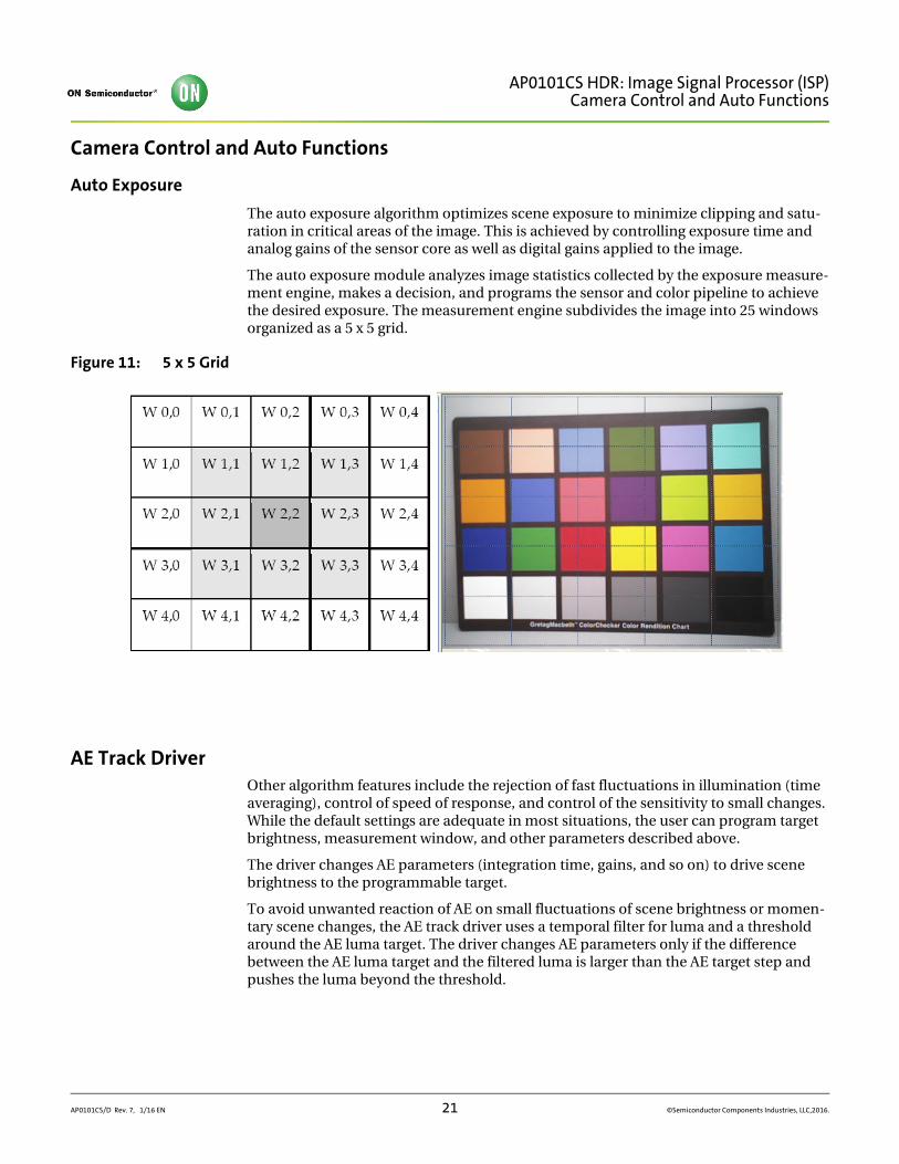
The auto exposure module analyzes image statistics collected by the exposure measure-ment engine, makes a decision, and programs the sensor and color pipeline to achieve the desired exposure. The measurement engine subdivides the image into 25 windows organized as a 5 x 5 grid.
Figure 11: 5 x 5 Grid
AE Track DriverOther algorithm features include the rejection of fast fluctuations in illumination (time averaging), control of speed of response, and control of the sensitivity to small changes. While the default settings are adequate in most situations, the user can program target brightness, measurement window, and other parameters described above.
The driver changes AE parameters (integration time, gains, and so on) to drive scene brightness to the programmable target.
To avoid unwanted reaction of AE on small fluctuations of scene brightness or momen-tary scene changes, the AE track driver uses a temporal filter for luma and a threshold around the AE luma target. The driver changes AE parameters only if the difference between the AE luma target and the filtered luma is larger than the AE target step and pushes the luma beyond the threshold.
AP0101CS/D Rev. 7, 1/16 EN 21 ©Semiconductor Components Industries, LLC,2016.
AP0101CS HDR: Image Signal Processor (ISP)Auto White Balance
Auto White BalanceThe AP0101CS has a built-in AWB algorithm designed to compensate for the effects of changing spectra of the scene illumination on the quality of the color rendition. The algorithm consists of two major parts: a measurement engine performing statistical analysis of the image and a driver performing the selection of the optimal color correc-tion matrix and IFP digital gain. While default settings of these algorithms are adequate in most situations, the user can reprogram base color correction matrices, place limits on color channel gains, and control the speed of both matrix and gain adjustments. The AP0101CS AWB displays the current AWB position in color temperature, the range of which will be defined when programming the CCM matrixes.
The region of interest can be controlled through the combination of an inclusion window and an exclusion window.
Dual Band IRCFFor some applications a day/night filter would be switched in/out, this option is an additional cost to the camera system. The AP0101CS supports the use of dual band IRCF, which removes the need for the switching day/night filter. Tuning support is provided for this usage case. Refer to the AP0101CS developer guide for details.
Exposure and White Balance ModesAP0101CS supports auto and manual exposure and white balance modes. In addition, it will operate within synchronized multi-camera systems. In this use case, one camera within the system will be the 'master', and the others 'slaves'. The master is used to calculate the appropriate exposure and white balance. This is then applied to all slaves concurrently under host control.
Auto Mode
In Auto Exposure mode the AE algorithm is responsible for calculating the appropriate exposure to keep the desired scene brightness, and for applying the exposure to the underlying hardware. In Auto White Balance mode the AWB algorithm is responsible for calculating the color temperature of the scene and applying the appropriate red and blue gains.
Triggered Auto mode
The Triggered Auto Exposure and Triggered Auto White Balance modes are intended for the multi-camera use cases, where a host is controlling the exposure and white balance of a number of cameras. The idea is that one camera is in triggered-auto mode (the master), and the others in host-controlled mode (slaves). The master camera must calculate the exposure and gains, the host then copies this to the slaves, and all changes are then applied at the same time.
Manual Mode
Manual mode is intended to allow simple manual exposure and white balance control by the host. The host needs to set the CAM_AET_EXPOSURE_TIME_MS, CAM_AET_EX-POSURE_GAIN and CAM_AWB_COLOR_TEMPERATURE controls, the camera will calculate the appropriate integration times and gains.
AP0101CS/D Rev. 7, 1/16 EN 22 ©Semiconductor Components Industries, LLC,2016.
AP0101CS HDR: Image Signal Processor (ISP)Flicker Avoidance
Host Controlled
The Host Controlled mode is intended to give the host full control over exposure and gains.
Flicker AvoidanceFlicker occurs when the integration time is not an integer multiple of the period of the light intensity. The AP0101CS can be programmed to avoid flicker for 50 or 60 Hertz. For integration times less than the light intensity period (10ms for 50Hz environment), flicker cannot be avoided. The AP0101CS supports an indoor AE mode, that will ensure flicker-free operation.
Output FormattingThe AP0101CS can output pixel data as an 8 or 10 bit word, over one or two clocks per pixel. AP0101AT supports parallel output & SMPTE modes.
Uncompressed YCbCr Data Ordering
The AP0101CS supports swapping YCbCr mode, as illustrated in Table 11.
The data ordering for the YCbCr output modes for AP0101CS are shown in Table 12 and Table 13:
Note: Odd means first cycle; even means second cycle.
Table 11: YCbCr Output Data Ordering
Mode Data Sequence
Default (no swap) Cbi Yi Cri Yi+1
Swapped CrCb Cri Yi Cbi Yi+1
Swapped YC Yi Cbi Yi+1 Cri
Swapped CrCb, YC Yi Cri Yi+1 Cbi
Table 12: YCbCr Output Modes (cam_port_parallel_msb_align=0x1, cam_port_parallel_swap_bytes = 0, cam_output_format_yuv_swap_red_blue = 0)
Mode Byte Pixel i Pixel i+1 Notes
YCbCr_422_8_8Odd (DOUT [15:8]) Cbi Cri Data range of 0-255 (Y=16-235 and C=16-240)
Even (DOUT [15:8]) Yi Yi+1
YCbCr_422_10_10Odd (DOUT [15:6]) Cbi Cri
Data range of 0-1023 (Y=64-940 and C=64-960)
Even (DOUT [15:6]) Yi Yi+1
YCbCr_422_16 Single (DOUT [15:0]) Cbi_Yi Cri_Yi+1 Data range of 0-255 (Y=16-235 and C=16-240)
Table 13: YCbCr Output Modes (cam_port_parallel_msb_align=0x0, cam_port_parallel_swap_bytes = 0, cam_output_format_yuv_swap_red_blue = 0)
Mode Byte Pixel i Pixel i+1 Notes
YCbCr_422_8_8Odd (DOUT[7 :0]) Cbi Cri Data range of 0-255 (Y=16-235 and C=16-240)
Even (DOUT [7:0] Yi Yi+1
AP0101CS/D Rev. 7, 1/16 EN 23 ©Semiconductor Components Industries, LLC,2016.
AP0101CS HDR: Image Signal Processor (ISP)Output Formatting
Figure 12: 8- bit YCbCr Output (YCbCr_422_8_8)
Note: cam_port_parallel_msb_align = 0cam_port_parallel_swap_bytes = 1cam_output_format_yuv_swap_red_blue = 0
YCbCr_422_10_10 Odd (DOUT [9:0]) Cbi Cri Data range of 0-1023 (Y=64-940 and C=64-960)"
Even (DOUT [9:0]) Yi Yi+1
YCbCr_422_16 Single (DOUT [15:0]) Cbi_Yi Cri_Yi+1 Data range of 0-255 (Y=16-235 and C=16-240)
Table 13: YCbCr Output Modes (cam_port_parallel_msb_align=0x0, cam_port_parallel_swap_bytes = 0, cam_output_format_yuv_swap_red_blue = 0)
Mode Byte Pixel i Pixel i+1 Notes
Active Video
Y C b Y C r Y C b Y C r Y C b Y C r Y C b Y C r
Im age Im ageH Blank H Blank H Blank
Vertical Blanking
Y Cb Y Cr
Vblank Im age
VblankY Cb Y Cr
Im age
Y Cb Y C r Y Cb Y Cr Y Cb Y Cr Y Cb Y Cr
Im age Im ageH Blank H Blank H Blank
00
00
00
00
C r
C r
C r
Line V alid
F ram e V alid
P ix el C loc k
Data[15:8]
Data[7:0]
Line V alid
F ram e V alid
P ix el C loc k
Data[15:8]
Data[7:0]
Line V alid
F ram e V alid
P ix el C loc k
Data[15:8]
Data[7:0]
Porch – 0-255 cycles
Line V alid
F ram e V alid
P ix el C loc k
Data[15:8]
Data[7:0]
Porch – 0-255 cycles
Porch – 0-255 cycles
Porch – 0-255 cycles
AP0101CS/D Rev. 7, 1/16 EN 24 ©Semiconductor Components Industries, LLC,2016.
AP0101CS HDR: Image Signal Processor (ISP)Output Formatting
Figure 13: 10-bit YCbCr Output (YCbCr_422_10_10)
Note: cam_port_parallel_msb_align = 1cam_port_parallel_swap_bytes = 1cam_output_format_yuv_swap_red_blue = 0
Active Video
Y Cb Y Cr Y C b Y C r Y Cb Y Cr Y Cb Y C r
Im age Im ageH Blank H Blank H Blank
Vertical Blanking
Y Cb Y Cr
Vblank Im age
VblankY Cb Y C r
Im age
Y Cb Y Cr Y Cb Y C r Y Cb Y Cr Y Cb Y C r
Im age Im ageH Blank H Blank H Blank
00
00
00
00
C r
C r
C r
Line V alid
F ram e V alid
P ix el C loc k
Data[5:0]
Data[15:6]
Line V alid
F ram e V alid
P ix el C loc k
Data[5:0]
Data[15:6]
Line V alid
F ram e V alid
P ix el C loc k
Data[5:0]
Data[15:6]
Line V alid
F ram e V alid
P ix el C loc k
Data[5:0]
Data[15:6]
Porch – 0-255 cycles
Porch – 0-255 cycles
Porch – 0-255 cycles
Porch – 0-255 cycles
AP0101CS/D Rev. 7, 1/16 EN 25 ©Semiconductor Components Industries, LLC,2016.
AP0101CS HDR: Image Signal Processor (ISP)Output Formatting
Figure 14: 16-bit YCbCr Output (YCbCr_422_16)
Note: cam_port_parallel_swap_bytes = 0cam_output_format_yuv_swap_red_blue = 0
Active Video
Cb Cr Cb C r Cb Cr Cb C r Cb Cr Cb Cr Cb Cr Cb C r
Im age Im ageH Blank H Blank H Blank
Vertical Blanking
C b C r C b C r
Vblank Im age
VblankC b C r C b C r
Im age
Im age Im ageH Blank H Blank H Blank
C r
C r
Y Y Y Y Y Y Y Y Y Y Y Y Y Y Y YY
Cb Cr Cb Cr Cb Cr Cb C r Cb Cr Cb C r Cb Cr Cb C rC r
Y Y Y Y Y Y Y Y Y Y Y Y Y Y Y YY
Y Y Y Y
Y Y Y YY
Line Valid
Frame Valid
Pixel Clock
Data[7:0]
Data[15:8]
Line Valid
Frame Valid
Pixel Clock
Data[7:0]
Data[15:8]
Line Valid
Frame Valid
Pixel Clock
Data[7:0]
Data[15:8]
Line Valid
Frame Valid
Pixel Clock
Data[7:0]
Data[15:0]
Porch – 0-255 cycles
Porch – 0-255 cycles
Porch – 0-255 cycles
Porch – 0-255 cycles
AP0101CS/D Rev. 7, 1/16 EN 26 ©Semiconductor Components Industries, LLC,2016.
AP0101CS HDR: Image Signal Processor (ISP)Output Formatting
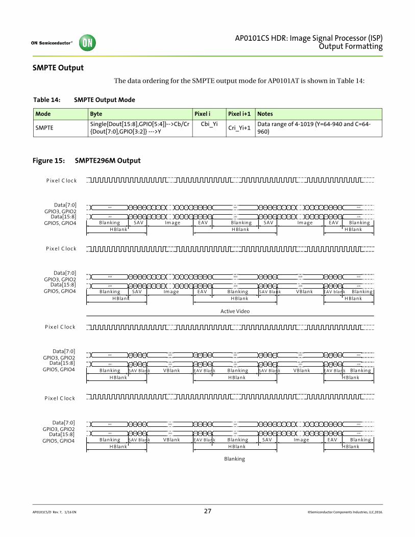
SMPTE Output
The data ordering for the SMPTE output mode for AP0101AT is shown in Table 14:
Figure 15: SMPTE296M Output
Table 14: SMPTE Output Mode
Mode Byte Pixel i Pixel i+1 Notes
SMPTESingle{Dout[15:8],GPIO[5:4]}-->Cb/Cr{Dout[7:0],GPIO[3:2]} --->Y
Cbi_YiCri_Yi+1
Data range of 4-1019 (Y=64-940 and C=64-960)
Active Video
C b C r C b C r C b C r C b C r 200 C b C r C b C r3F F 000 000 200200 3F F 000 000 274 3F F 000 000 200 C b C r C b C r 2003F F 000 000 274
SAV Im age EAV SAV Im age EAVH Blank H Blank
BlankingBlanking BlankingH Blank
SAV Im age EAV SAV Blank VBlank EAV blank
H Blank H BlankBlankingBlanking Blanking
H Blank
SAV Blank VBlank EAV Blank SAV Blank VBlank EAV Blank
H Blank H Blank
BlankingBlanking Blanking
H Blank
SAV Blank VBlank EAV Blank SAV Im age EAVH Blank H Blank
BlankingBlanking BlankingH Blank
Blanking
Y Y Y Y Y Y Y Y 040 Y Y Y Y3F F 000 000 200040 3F F 000 000 274 3F F 000 000 200 Y Y Y Y 0403F F 000 000 274
Y Y Y Y Y Y Y Y 040 0403FF 000 000 200040 000 000 274 000 000 040000 000 2D8
C b C r C b C r C b C r C b C r 200 200000 000 200200 000 000 274 000 000 200000 000
040 040 040000 000040 000 000 000 000 040000 000
200 200 200000 000200 000 000 000 000 2AC 200000 000
040 040 Y Y Y Y3F F 000 000 2AC040 3F F 000 000 2D8 3F F 000 000 200 Y Y Y Y 0403F F 000 000 274
200 200 C b C r C b C r3F F 000 000 2AC200 3F F 000 000 2D8 3F F 000 000 200 C b C r C b C r 2003F F 000 000 274
P ix el C loc k
Data[7:0]GPIO3, GPIO2
Data[15:8]GPIO5, GPIO4
P ix el C loc k
Data[7:0]GPIO3, GPIO2
Data[15:8]GPIO5, GPIO4
P ix el C loc k
Data[7:0]GPIO3, GPIO2
Data[15:8]GPIO5, GPIO4
P ix el C loc k
Data[7:0]GPIO3, GPIO2
Data[15:8]GPIO5, GPIO4
3FF
3FF
3FF
3FF
3FF
3FF
3FF 2D8
2D8
2D8
2AC
2AC
2AC
3FF
3FF
3FF
3FF
3FF
3FF
3FF
3FF 2AC
2AC 2D8
2D8
AP0101CS/D Rev. 7, 1/16 EN 27 ©Semiconductor Components Industries, LLC,2016.
AP0101CS HDR: Image Signal Processor (ISP)Sensor Embedded Data
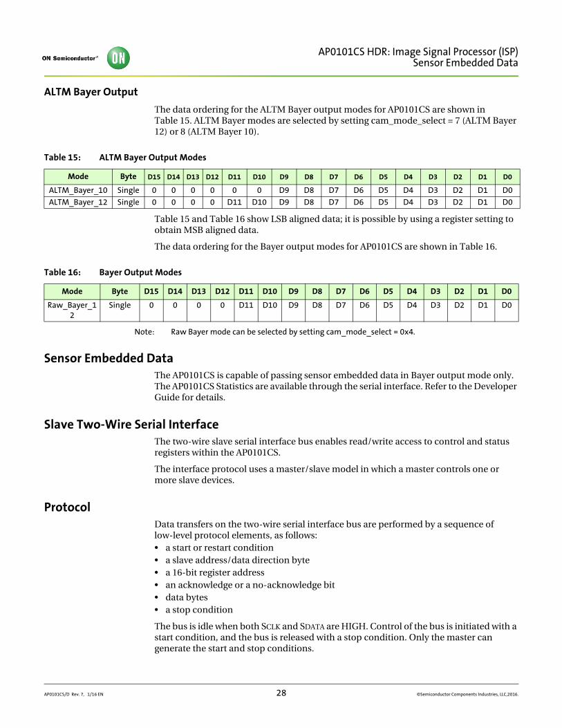
ALTM Bayer Output
The data ordering for the ALTM Bayer output modes for AP0101CS are shown in Table 15. ALTM Bayer modes are selected by setting cam_mode_select = 7 (ALTM Bayer 12) or 8 (ALTM Bayer 10).
Table 15 and Table 16 show LSB aligned data; it is possible by using a register setting to obtain MSB aligned data.
The data ordering for the Bayer output modes for AP0101CS are shown in Table 16.
Note: Raw Bayer mode can be selected by setting cam_mode_select = 0x4.
Sensor Embedded DataThe AP0101CS is capable of passing sensor embedded data in Bayer output mode only. The AP0101CS Statistics are available through the serial interface. Refer to the Developer Guide for details.
Slave Two-Wire Serial InterfaceThe two-wire slave serial interface bus enables read/write access to control and status registers within the AP0101CS.
The interface protocol uses a master/slave model in which a master controls one or more slave devices.
ProtocolData transfers on the two-wire serial interface bus are performed by a sequence of low-level protocol elements, as follows:• a start or restart condition• a slave address/data direction byte• a 16-bit register address• an acknowledge or a no-acknowledge bit • data bytes• a stop condition
The bus is idle when both SCLK and SDATA are HIGH. Control of the bus is initiated with a start condition, and the bus is released with a stop condition. Only the master can generate the start and stop conditions.
Table 15: ALTM Bayer Output Modes
Mode Byte D15 D14 D13 D12 D11 D10 D9 D8 D7 D6 D5 D4 D3 D2 D1 D0
ALTM_Bayer_10 Single 0 0 0 0 0 0 D9 D8 D7 D6 D5 D4 D3 D2 D1 D0
ALTM_Bayer_12 Single 0 0 0 0 D11 D10 D9 D8 D7 D6 D5 D4 D3 D2 D1 D0
Table 16: Bayer Output Modes
Mode Byte D15 D14 D13 D12 D11 D10 D9 D8 D7 D6 D5 D4 D3 D2 D1 D0
Raw_Bayer_12
Single 0 0 0 0 D11 D10 D9 D8 D7 D6 D5 D4 D3 D2 D1 D0
AP0101CS/D Rev. 7, 1/16 EN 28 ©Semiconductor Components Industries, LLC,2016.
AP0101CS HDR: Image Signal Processor (ISP)Protocol
The SADDR pin is used to select between two different addresses in case of conflict with another device. If SADDR is LOW, the slave address is 0x90; if SADDR is HIGH, the slave address is 0xBA. See Table 17 below. The user can change the slave address by changing a register value.
Start Condition
A start condition is defined as a HIGH-to-LOW transition on SDATA while SCLK is HIGH.
At the end of a transfer, the master can generate a start condition without previously generating a stop condition; this is known as a “repeated start” or “restart” condition.
Data Transfer
Data is transferred serially, 8 bits at a time, with the MSB transmitted first. Each byte of data is followed by an acknowledge bit or a no-acknowledge bit. This data transfer mechanism is used for the slave address/data direction byte and for message bytes. One data bit is transferred during each SCLK clock period. SDATA can change when SCLK is low and must be stable while SCLK is HIGH.
Slave Address/Data Direction Byte
Bits [7:1] of this byte represent the device slave address and bit [0] indicates the data transfer direction. A “0” in bit [0] indicates a write, and a “1” indicates a read. The default slave addresses used by the AP0101CS are 0x90 (write address) and 0x91 (read address). Alternate slave addresses of 0xBA (write address) and 0xBB (read address) can be selected by asserting the SADDR input signal.
Message Byte
Message bytes are used for sending register addresses and register write data to the slave device and for retrieving register read data. The protocol used is outside the scope of the two-wire serial interface specification.
Acknowledge Bit
Each 8-bit data transfer is followed by an acknowledge bit or a no-acknowledge bit in the SCLK clock period following the data transfer. The transmitter (which is the master when writing, or the slave when reading) releases SDATA. The receiver indicates an acknowl-edge bit by driving SDATA LOW. As for data transfers, SDATA can change when SCLK is LOW and must be stable while SCLK is HIGH.
No-Acknowledge Bit
The no-acknowledge bit is generated when the receiver does not drive SDATA low during the SCLK clock period following a data transfer. A no-acknowledge bit is used to termi-nate a read sequence.
Table 17: Two-Wire Interface ID Address Switching
SADDR Two-Wire Interface Address ID
0 0x90
1 0xBA
AP0101CS/D Rev. 7, 1/16 EN 29 ©Semiconductor Components Industries, LLC,2016.
AP0101CS HDR: Image Signal Processor (ISP)Protocol
Stop Condition
A stop condition is defined as a LOW-to-HIGH transition on SDATA while SCLK is HIGH.
Typical Operation
A typical READ or WRITE sequence begins by the master generating a start condition on the bus. After the start condition, the master sends the 8-bit slave address/data direction byte. The last bit indicates whether the request is for a READ or a WRITE, where a “0” indicates a WRITE and a “1” indicates a READ. If the address matches the address of the slave device, the slave device acknowledges receipt of the address by generating an acknowledge bit on the bus.
If the request was a WRITE, the master then transfers the 16-bit register address to which a WRITE will take place. This transfer takes place as two 8-bit sequences and the slave sends an acknowledge bit after each sequence to indicate that the byte has been received. The master will then transfer the 8-bit or 16-bit data, as one or two 8-bit sequences and the slave sends an acknowledge bit after each sequence to indicate that the byte has been received. The master stops writing by generating a (re)start or stop condition. If the request was a READ, the master sends the 8-bit write slave address/data direction byte and 16-bit register address, just as in the write request. The master then generates a (re)start condition and the 8-bit read slave address/data direction byte, and clocks out the register data, 8 bits at a time. The master generates an acknowledge bit after each 8-bit transfer. The data transfer is stopped when the master sends a no-acknowledge bit.
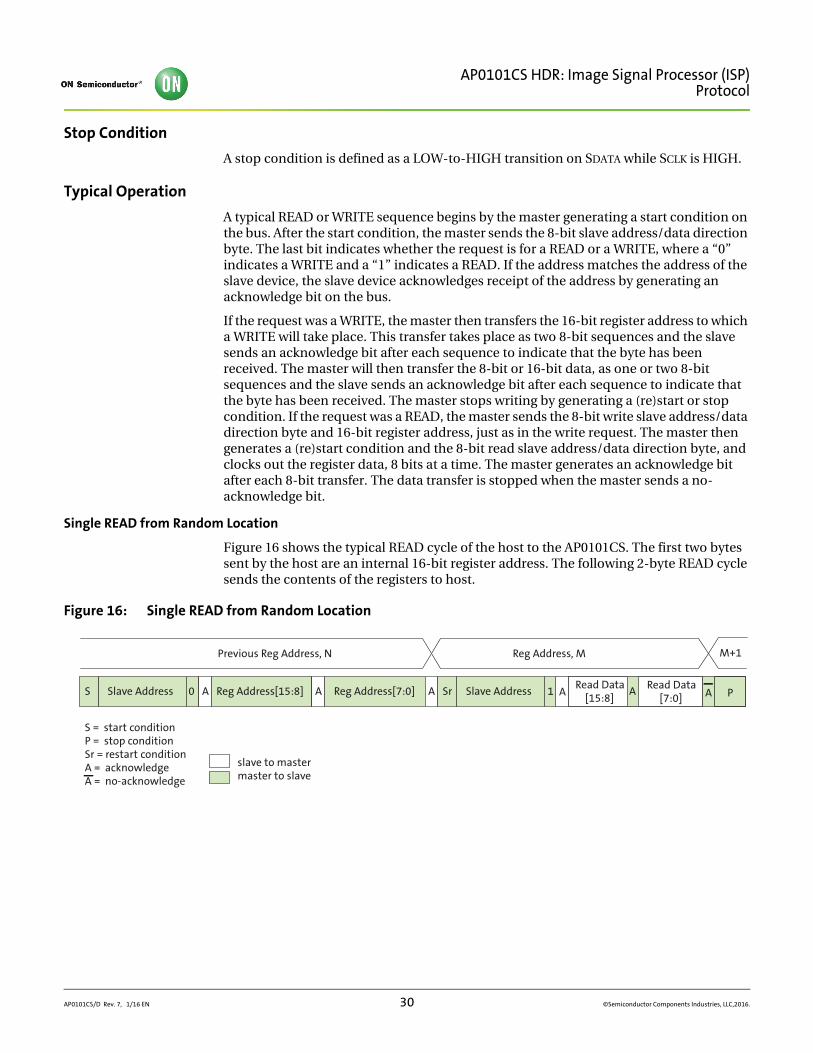
Single READ from Random Location
Figure 16 shows the typical READ cycle of the host to the AP0101CS. The first two bytes sent by the host are an internal 16-bit register address. The following 2-byte READ cycle sends the contents of the registers to host.
Figure 16: Single READ from Random Location
S = start conditionP = stop conditionSr = restart conditionA = acknowledgeA = no-acknowledge
slave to mastermaster to slave
Slave Address 0S A Reg Address[15:8] A Reg Address[7:0] Slave Address AA 1SrRead Data
[15:8] P
Previous Reg Address, N Reg Address, M M+1
ARead Data
[7:0]A
AP0101CS/D Rev. 7, 1/16 EN 30 ©Semiconductor Components Industries, LLC,2016.
AP0101CS HDR: Image Signal Processor (ISP)Protocol
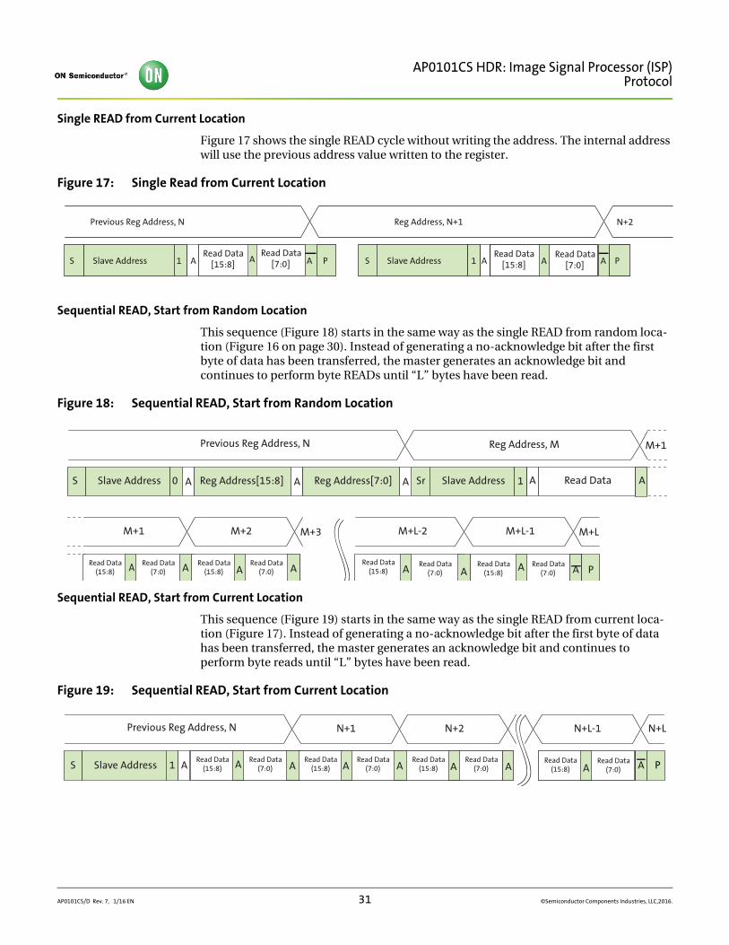
Single READ from Current Location
Figure 17 shows the single READ cycle without writing the address. The internal address will use the previous address value written to the register.
Figure 17: Single Read from Current Location
Sequential READ, Start from Random Location
This sequence (Figure 18) starts in the same way as the single READ from random loca-tion (Figure 16 on page 30). Instead of generating a no-acknowledge bit after the first byte of data has been transferred, the master generates an acknowledge bit and continues to perform byte READs until “L” bytes have been read.
Figure 18: Sequential READ, Start from Random Location
Sequential READ, Start from Current Location
This sequence (Figure 19) starts in the same way as the single READ from current loca-tion (Figure 17). Instead of generating a no-acknowledge bit after the first byte of data has been transferred, the master generates an acknowledge bit and continues to perform byte reads until “L” bytes have been read.
Figure 19: Sequential READ, Start from Current Location
Slave Address 1S ARead Data
[15:8] Slave Address A1SPRead Data
[15:8] P
Previous Reg Address, N Reg Address, N+1 N+2
AARead Data
[7:0]A Read Data[7:0]A
Read Data(15:8) A A Read Data
(15:8) A Read Data(7:0)
A
Slave Address 0S SrA Reg Address[15:8] A Reg Address[7:0] A Read DataSlave Address
Previous Reg Address, N Reg Address, M
M+1 M+2
M+1
M+3
A1
M+L-2 M+L-1 M+L
A P
A
Read Data(15:8) A Read Data
(7:0) A Read Data(15:8) A Read Data
(7:0) A Read Data(7:0)A A A A A A
ARead Data Read Data
Previous Reg Address, N N+1 N+2 N+L-1 N+L
ARead DataSlave Address AA1 AS PRead Data
(15:8) A Read Data(7:0) A Read Data
(15:8) A Read Data(7:0) A Read Data
(15:8) A Read Data(7:0) A
Read DataRead Data(15:8) A Read Data
(7:0)A A A A A A A
AP0101CS/D Rev. 7, 1/16 EN 31 ©Semiconductor Components Industries, LLC,2016.
AP0101CS HDR: Image Signal Processor (ISP)Protocol
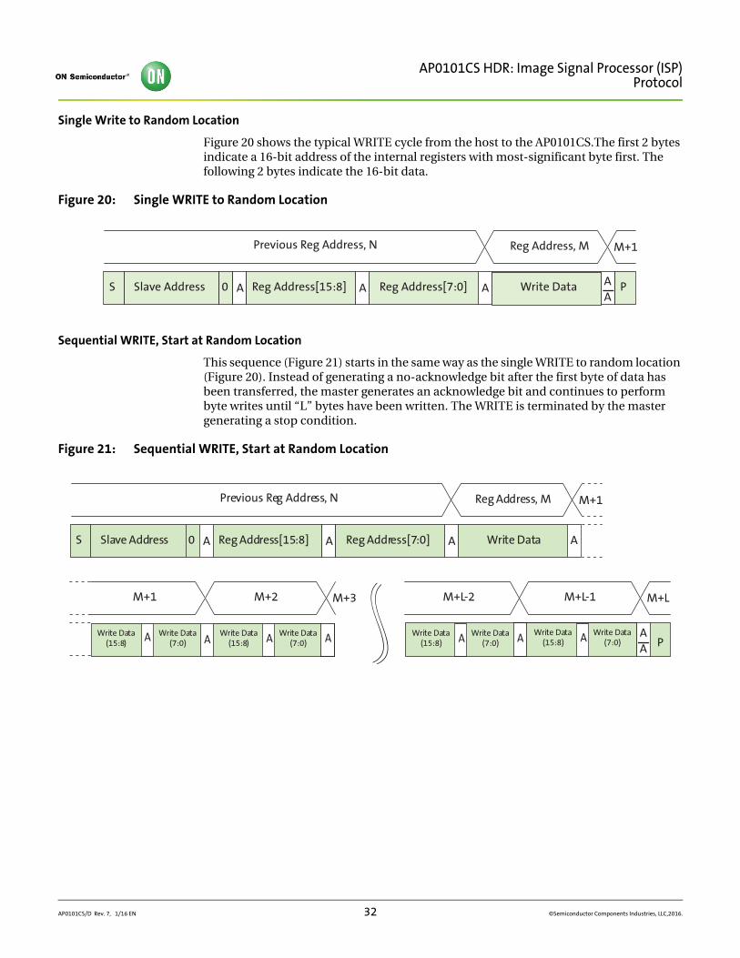
Single Write to Random Location
Figure 20 shows the typical WRITE cycle from the host to the AP0101CS.The first 2 bytes indicate a 16-bit address of the internal registers with most-significant byte first. The following 2 bytes indicate the 16-bit data.
Figure 20: Single WRITE to Random Location
Sequential WRITE, Start at Random Location
This sequence (Figure 21) starts in the same way as the single WRITE to random location (Figure 20). Instead of generating a no-acknowledge bit after the first byte of data has been transferred, the master generates an acknowledge bit and continues to perform byte writes until “L” bytes have been written. The WRITE is terminated by the master generating a stop condition.
Figure 21: Sequential WRITE, Start at Random Location
Slave Address 0S A Reg Address[15:8] A Reg Address[7:0] A P
Previous Reg Address, N Reg Address, M M+1
AA
Write Data
Slave Address 0S A Reg Address[15:8]
Write Data
A Reg Address[7:0] A Write Data
Previous Reg Address, N Reg Address, M
M+1 M+2
M+1
M+3
A
AA Write Data Write Data
M+L-2 M+L-1 M+L
AA P
Write Data(15:8)
Write Data(7:0)
Write Data(15:8) A Write Data
(7:0)A AA A Write Data AWrite Data
(15:8) A Write Data(7:0) A Write DataWrite Data
(15:8) A Write Data(7:0)
AP0101CS/D Rev. 7, 1/16 EN 32 ©Semiconductor Components Industries, LLC,2016.
AP0101CS HDR: Image Signal Processor (ISP)Usage Modes
Device Configuration and Usage Modes
After power is applied and the device is out of reset (either the power on reset, hard or soft reset), it will enter a boot sequence to configure its operating mode. There are essen-tially three configuration modes: Flash/EEPROM Config, Auto Config, and Host Config.
The AP0101CS firmware supports a System Configuration phase at start-up. This consists of four sub-phases of execution:1. Flash detection, then one of:
a. Flash Configb. Auto Configc. Host Config
The System Configuration phase is entered immediately following power-up or reset. Then the firmware performs Flash Detection.
Flash Detection attempts to detect the presence of an SPI Flash or EEPROM device:• If no device is detected, the firmware then samples the SPI_SDI pin state to determine
the next mode:– If SPI_SDI is low, then it enters the Host-Config mode.– If SPI_SDI is high, then it enters the Auto-Config mode.
• If a device is detected, the firmware switches to the Flash-Config mode.
In the Flash-Config mode, the firmware interrogates the device to determine if it contains valid configuration records:• If no records are detected, then the firmware enters the Auto-Config mode.• If records are detected, the firmware processes them. By default, when all Flash
records are processed the firmware switches to the Host-Config mode. However, the records encoded into the Flash can optionally be used to instruct the firmware to proceed to auto-config, or to start streaming (via a Change-Config).
In the Host-Config mode, the firmware performs no configuration, and remains idle waiting for configuration and commands from the host. The System Configuration phase is effectively complete and the AP0101CS will take no actions until the host issues commands.
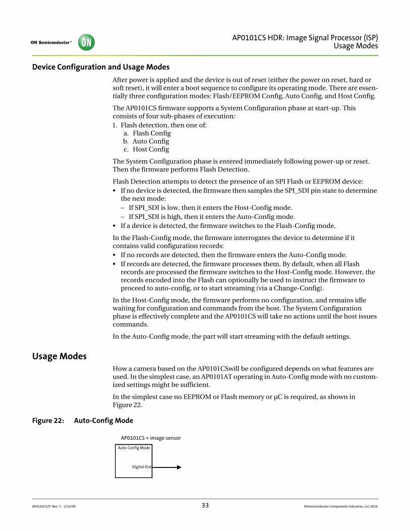
In the Auto-Config mode, the part will start streaming with the default settings.
Usage ModesHow a camera based on the AP0101CSwill be configured depends on what features are used. In the simplest case, an AP0101AT operating in Auto-Config mode with no custom-ized settings might be sufficient.
In the simplest case no EEPROM or Flash memory or µC is required, as shown in Figure 22.
Figure 22: Auto-Config Mode
Digital Out
Auto-Config Mode
AP0101CS + image sensor
AP0101CS/D Rev. 7, 1/16 EN 33 ©Semiconductor Components Industries, LLC,2016.
AP0101CS HDR: Image Signal Processor (ISP)Host Command Interface
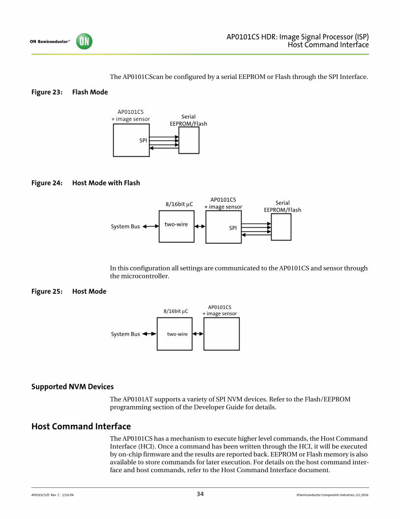
The AP0101CScan be configured by a serial EEPROM or Flash through the SPI Interface.
Figure 23: Flash Mode
Figure 24: Host Mode with Flash
In this configuration all settings are communicated to the AP0101CS and sensor through the microcontroller.
Figure 25: Host Mode
Supported NVM Devices
The AP0101AT supports a variety of SPI NVM devices. Refer to the Flash/EEPROM programming section of the Developer Guide for details.
Host Command InterfaceThe AP0101CS has a mechanism to execute higher level commands, the Host Command Interface (HCI). Once a command has been written through the HCI, it will be executed by on-chip firmware and the results are reported back. EEPROM or Flash memory is also available to store commands for later execution. For details on the host command inter-face and host commands, refer to the Host Command Interface document.
SerialEEPROM/Flash
SPI
AP0101CS+ image sensor
AP0101CS+ image sensor
SPI
8/16bit μC
two-wireSystem Bus
SerialEEPROM/Flash
8/16bit μC
two-wireSystem Bus
AP0101CS+ image sensor
AP0101CS/D Rev. 7, 1/16 EN 34 ©Semiconductor Components Industries, LLC,2016.
AP0101CS HDR: Image Signal Processor (ISP)Electrical Specifications
Electrical Specifications
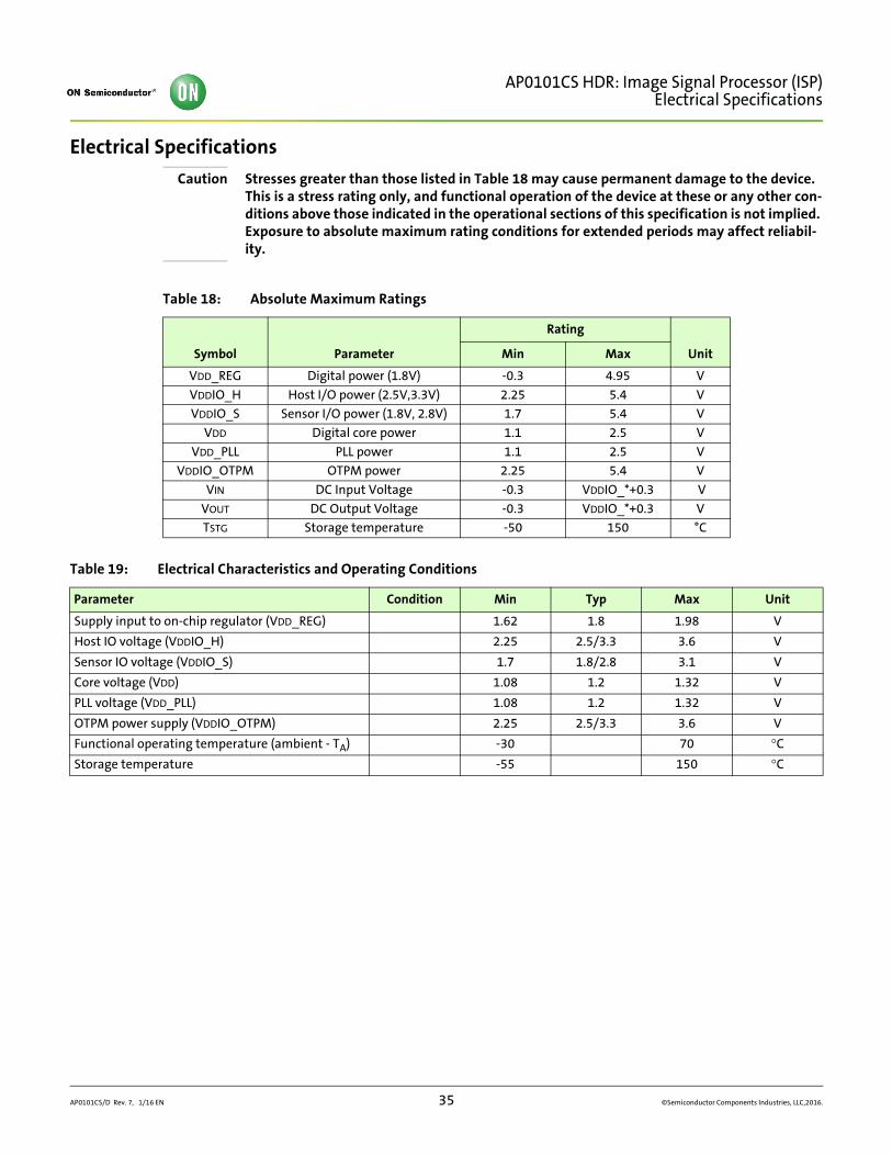
Caution Stresses greater than those listed in Table 18 may cause permanent damage to the device. This is a stress rating only, and functional operation of the device at these or any other con-ditions above those indicated in the operational sections of this specification is not implied. Exposure to absolute maximum rating conditions for extended periods may affect reliabil-ity.
Table 18: Absolute Maximum Ratings
Symbol Parameter
Rating
Unit Min Max
VDD_REG Digital power (1.8V) -0.3 4.95 V
VDDIO_H Host I/O power (2.5V,3.3V) 2.25 5.4 V
VDDIO_S Sensor I/O power (1.8V, 2.8V) 1.7 5.4 V
VDD Digital core power 1.1 2.5 V
VDD_PLL PLL power 1.1 2.5 V
VDDIO_OTPM OTPM power 2.25 5.4 V
VIN DC Input Voltage -0.3 VDDIO_*+0.3 V
VOUT DC Output Voltage -0.3 VDDIO_*+0.3 V
TSTG Storage temperature -50 150 °C
Table 19: Electrical Characteristics and Operating Conditions
Parameter Condition Min Typ Max Unit
Supply input to on-chip regulator (VDD_REG) 1.62 1.8 1.98 V
Host IO voltage (VDDIO_H) 2.25 2.5/3.3 3.6 V
Sensor IO voltage (VDDIO_S) 1.7 1.8/2.8 3.1 V
Core voltage (VDD) 1.08 1.2 1.32 V
PLL voltage (VDD_PLL) 1.08 1.2 1.32 V
OTPM power supply (VDDIO_OTPM) 2.25 2.5/3.3 3.6 V
Functional operating temperature (ambient - TA) -30 70 °C
Storage temperature -55 150 °C
AP0101CS/D Rev. 7, 1/16 EN 35 ©Semiconductor Components Industries, LLC,2016.
AP0101CS HDR: Image Signal Processor (ISP)Electrical Specifications
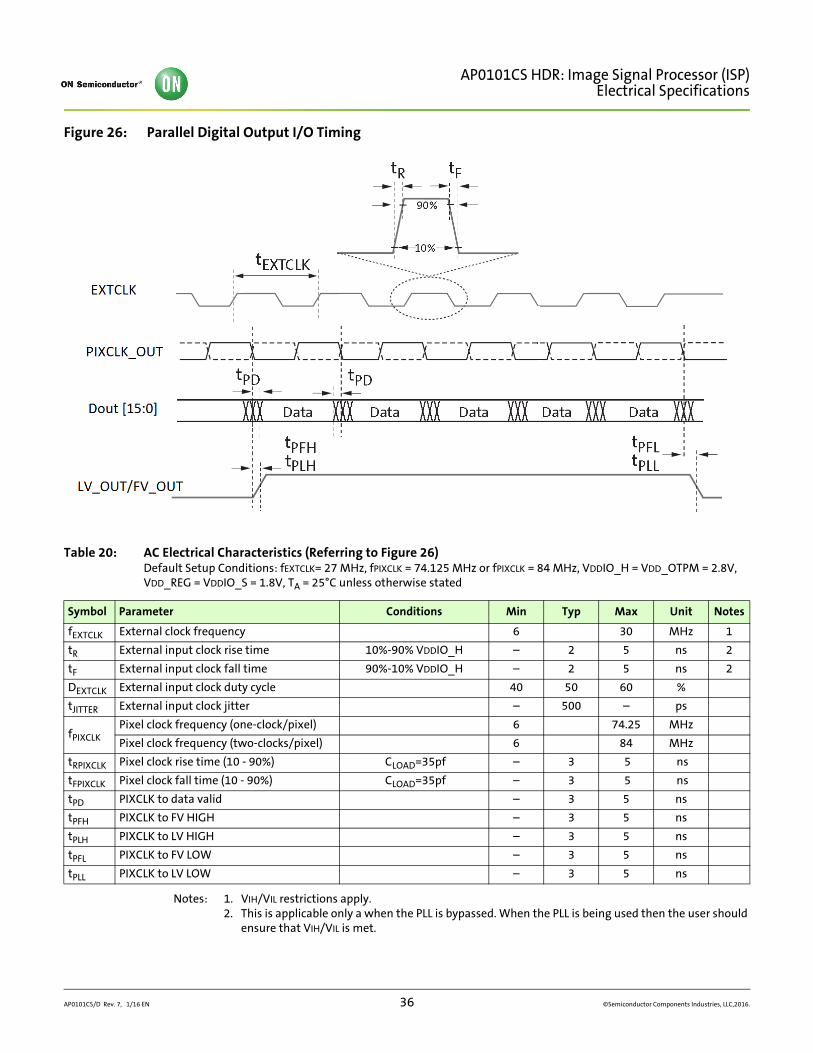
Figure 26: Parallel Digital Output I/O Timing
Notes: 1. VIH/VIL restrictions apply.2. This is applicable only a when the PLL is bypassed. When the PLL is being used then the user should
ensure that VIH/VIL is met.
Table 20: AC Electrical Characteristics (Referring to Figure 26)Default Setup Conditions: fEXTCLK= 27 MHz, fPIXCLK = 74.125 MHz or fPIXCLK = 84 MHz, VDDIO_H = VDD_OTPM = 2.8V, VDD_REG = VDDIO_S = 1.8V, TA = 25°C unless otherwise stated
Symbol Parameter Conditions Min Typ Max Unit Notes
fEXTCLK External clock frequency 6 30 MHz 1
tR External input clock rise time 10%-90% VDDIO_H – 2 5 ns 2
tF External input clock fall time 90%-10% VDDIO_H – 2 5 ns 2
DEXTCLK External input clock duty cycle 40 50 60 %
tJITTER External input clock jitter – 500 – ps
fPIXCLK Pixel clock frequency (one-clock/pixel) 6 74.25 MHz
Pixel clock frequency (two-clocks/pixel) 6 84 MHz
tRPIXCLK Pixel clock rise time (10 - 90%) CLOAD=35pf – 3 5 ns
tFPIXCLK Pixel clock fall time (10 - 90%) CLOAD=35pf – 3 5 ns
tPD PIXCLK to data valid – 3 5 ns
tPFH PIXCLK to FV HIGH – 3 5 ns
tPLH PIXCLK to LV HIGH – 3 5 ns
tPFL PIXCLK to FV LOW – 3 5 ns
tPLL PIXCLK to LV LOW – 3 5 ns
AP0101CS/D Rev. 7, 1/16 EN 36 ©Semiconductor Components Industries, LLC,2016.
AP0101CS HDR: Image Signal Processor (ISP)Electrical Specifications
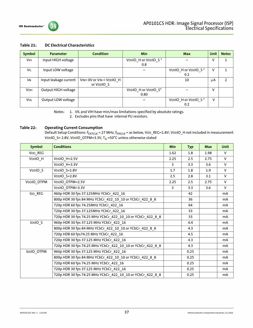
Notes: 1. VIL and VIH have min/max limitations specified by absolute ratings.2. Excludes pins that have internal PU resistors.
Table 21: DC Electrical Characteristics
Symbol Parameter Condition Min Max Unit Notes
VIH Input HIGH voltage VDDIO_H or VDDIO_S * 0.8
– V 1
VIL Input LOW voltage – VDDIO_H or VDDIO_S * 0.2
V 1
IIN Input leakage current VIN= 0V or VIN = VDDIO_H or VDDIO_S
10 A 2
VOH Output HIGH voltage VDDIO_H or VDDIO_S* 0.80
– V
VOL Output LOW voltage – VDDIO_H or VDDIO_S * 0.2
V
Table 22: Operating Current ConsumptionDefault Setup Conditions: fEXTCLK = 27 MHz, fPIXCLK = as below, VDD_REG=1.8V; VDDIO_H not included in measurementVDDIO_S= 2.8V, VDDIO_OTPM=3.3V, TA =50°C unless otherwise stated
Symbol Conditions Min Typ Max Unit
VDD_REG 1.62 1.8 1.98 V
VDDIO_H VDDIO_H=2.5V 2.25 2.5 2.75 V
VDDIO_H=3.3V 3 3.3 3.6 V
VDDIO_S VDDIO_S=1.8V 1.7 1.8 1.9 V
VDDIO_S=2.8V 2.5 2.8 3.1 V
VDDIO_OTPM VDDIO_OTPM=2.5V 2.25 2.5 2.75 V
VDDIO_OTPM=3.3V 3 3.3 3.6 V
IDD_REG 960p HDR 30 fps 37.125MHz YCbCr_422_16 42 mA
800p HDR 30 fps 84 MHz YCbCr_422_10_10 or YCbCr_422_8_8 36 mA
720p HDR 60 fps 74.25MHz YCbCr_422_16 64 mA
720p HDR 30 fps 37.125MHz YCbCr_422_16 33 mA
720p HDR 30 fps 74.25 MHz YCbCr_422_10_10 or YCbCr_422_8_8 33 mA
IDDIO_S 960p HDR 30 fps 37.125 MHz YCbCr_422_16 4.4 mA
800p HDR 30 fps 84 MHz YCbCr_422_10_10 or YCbCr_422_8_8 4.3 mA
720p HDR 60 fps74.25 MHz YCbCr_422_16 4.5 mA
720p HDR 30 fps 37.125 MHz YCbCr_422_16 4.3 mA
720p HDR 30 fps 74.25 MHz YCbCr_422_10_10 or YCbCr_422_8_8 4.3 mA
IDDIO_OTPM 960p HDR 30 fps 37.125 MHz YCbCr_422_16 0.25 mA
800p HDR 30 fps 84 MHz YCbCr_422_10_10 or YCbCr_422_8_8 0.25 mA
720p HDR 60 fps 74.25 MHz YCbCr_422_16 0.25 mA
720p HDR 30 fps 37.125 MHz YCbCr_422_16 0.25 mA
720p HDR 30 fps 74.25 MHz YCbCr_422_10_10 or YCbCr_422_8_8 0.25 mA
AP0101CS/D Rev. 7, 1/16 EN 37 ©Semiconductor Components Industries, LLC,2016.
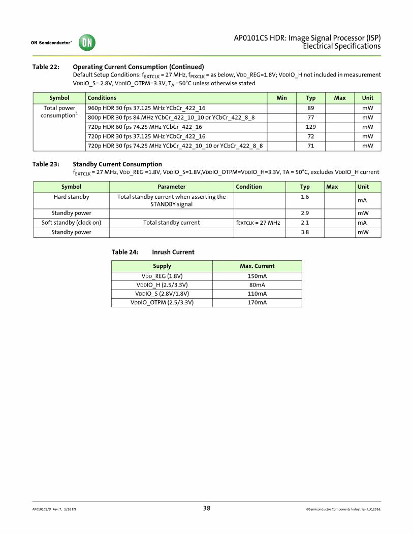
AP0101CS HDR: Image Signal Processor (ISP)Electrical Specifications
Total power consumption1
960p HDR 30 fps 37.125 MHz YCbCr_422_16 89 mW
800p HDR 30 fps 84 MHz YCbCr_422_10_10 or YCbCr_422_8_8 77 mW
720p HDR 60 fps 74.25 MHz YCbCr_422_16 129 mW
720p HDR 30 fps 37.125 MHz YCbCr_422_16 72 mW
720p HDR 30 fps 74.25 MHz YCbCr_422_10_10 or YCbCr_422_8_8 71 mW
Table 23: Standby Current ConsumptionfEXTCLK = 27 MHz, VDD_REG =1.8V, VDDIO_S=1.8V,VDDIO_OTPM=VDDIO_H=3.3V, TA = 50°C, excludes VDDIO_H current
Symbol Parameter Condition Typ Max Unit
Hard standby Total standby current when asserting the STANDBY signal
1.6 mA
Standby power 2.9 mW
Soft standby (clock on) Total standby current fEXTCLK = 27 MHz 2.1 mA
Standby power 3.8 mW
Table 24: Inrush Current
Supply Max. Current
VDD_REG (1.8V) 150mA
VDDIO_H (2.5/3.3V) 80mA
VDDIO_S (2.8V/1.8V) 110mA
VDDIO_OTPM (2.5/3.3V) 170mA
Table 22: Operating Current Consumption (Continued)Default Setup Conditions: fEXTCLK = 27 MHz, fPIXCLK = as below, VDD_REG=1.8V; VDDIO_H not included in measurementVDDIO_S= 2.8V, VDDIO_OTPM=3.3V, TA =50°C unless otherwise stated
Symbol Conditions Min Typ Max Unit
AP0101CS/D Rev. 7, 1/16 EN 38 ©Semiconductor Components Industries, LLC,2016.
AP0101CS HDR: Image Signal Processor (ISP)Two-Wire Serial Register Interface
Two-Wire Serial Register InterfaceThe electrical characteristics of the slave two-wire serial register interface (SCLK, SDATA) are shown in Figure 27 and Table 25.
Figure 27: Slave Two-Wire Serial Bus Timing Parameters (CCIS)
Notes: 1. All values referred to VIHmin = 0.9 VDD and VILmax = 0.1VDD levels. Sensor EXCLK = 27 MHz.2. A device must internally provide a hold time of at least 300 ns for the SDATA signal to bridge the
undefined region of the falling edge of SCLK.3. The maximum tHD;DAT has only to be met if the device does not stretch the LOW period (tLOW) of
the SCLK signal.4. Cb = total capacitance of one bus line in pF.
The electrical characteristics of the master two-wire serial register interface (M_SCLK, M_SDATA) are shown in Figure 28 and Table 26.
Table 25: Slave Two-Wire Serial Bus Characteristics (CCIS)Default Setup Conditions: fEXTCLK = 27 MHz, fPIXCLK = 74.125 MHz, VDDIO_H = VDD_OTPM = 2.8V, VDD_REG = VDDIO_S = 1.8V, Tj = 25°C unless otherwise stated
Parameter Symbol
Standard-Mode Fast-Mode
UnitMin Max Min Max
SCLK Clock Frequency fSCL 0 100 0 400 KHz
Hold time (repeated) START condition.
After this period, the first clock pulse is generated tHD;STA 4.0 - 0.6 - s
LOW period of the SCLK clock tLOW 4.7 - 1.3 - s
HIGH period of the SCLK clock tHIGH 4.0 - 0.6 - s
Set-up time for a repeated START condition tSU;STA 4.7 - 0.6 - s
Data hold time tHD;DAT 02 3.453 0 0.93 s
Data set-up time tSU;DAT 250 - 100 - ns
Rise time of both SDATA and SCLK signals tr - 1000 20 + 0.1Cb4 300 ns
Fall time of both SDATA and SCLK signals tf - 300 20 + 0.1Cb4 300 ns
Set-up time for STOP condition tSU;STO 4.0 - 0.6 - s
Bus free time between a STOP and START condition
tBUF 4.7 - 1.3 - s
Capacitive load for each bus line Cb - 400 - 400 pF
Serial interface input pin capacitance CIN_SI - 3.3 - 3.3 pF
SDATA max load capacitance CLOAD_SD - 30 - 30 pF
SDATA pull-up resistor RSD 1.5 4.7 1.5 4.7 K
S SrtSU;STOtSU;STAtHD;STA tHIGH
tLOW tSU;DAT
tHD;DAT
tf
SDATA
SCLK
P S
tBUFtrtftr tHD;STA
AP0101CS/D Rev. 7, 1/16 EN 39 ©Semiconductor Components Industries, LLC,2016.
AP0101CS HDR: Image Signal Processor (ISP)Two-Wire Serial Register Interface
Figure 28: Master Two-Wire Serial Bus Timing Parameters (CCIM)
Notes: 1. All values referred to VIHmin = 0.9 VDD and VILmax = 0.1VDD levels. Sensor EXCLK = 27 MHz.2. A device must internally provide a hold time of at least 300 ns for the M_SDATA signal to bridge the
undefined region of the falling edge of M_SCLK.3. The maximum tHD;DAT has only to be met if the device does not stretch the LOW period (tLOW) of
the M_SCLK signal.4. Cb = total capacitance of one bus line in pF.
Table 26: Master Two-Wire Serial Bus Characteristics (CCIM)Default Setup Conditions: fEXTCLK = 27 MHz, fPIXCLK = 74.125 MHz, VDDIO_H = VDD_OTPM = 2.8V, VDD_REG = VDDIO_S = 1.8V, Tj = 25°C unless otherwise stated
Parameter Symbol
Standard-Mode Fast-Mode
UnitMin Max Min Max
M_SCLK Clock Frequency fSCL 0 100 0 400 KHz
Hold time (repeated) START condition.
After this period, the first clock pulse is generated tHD;STA 4.0 - 0.6 - s
LOW period of the M_SCLK clock tLOW 4.7 - 1.2 - s
HIGH period of the M_SCLK clock tHIGH 4.0 - 0.6 - s
Set-up time for a repeated START condition tSU;STA 4.7 - 0.6 - s
Data hold time tHD;DAT 02 3.453 0 0.93 s
Data set-up time tSU;DAT 250 - 100 - ns
Rise time of both M_SDATA and M_SCLK signals tr - 1000 20 + 0.1Cb4 300 ns
Fall time of both M_SDATA and M_SCLK signals tf - 300 20 + 0.1Cb4 300 ns
Set-up time for STOP condition tSU;STO 4.0 - 0.6 - s
Bus free time between a STOP and START condition
tBUF 4.7 - 1.3 - s
Capacitive load for each bus line Cb - 400 - 400 pF
Serial interface input pin capacitance CIN_SI - 3.3 - 3.3 pF
M_SDATA max load capacitance CLOAD_SD - 30 - 30 pF
M_SDATA pull-up resistor RSD 1.5 4.7 1.5 4.7 K
S SrtSU;STOtSU;STAtHD;STA tHIGH
tLOW tSU;DAT
tHD;DAT
tf
SDATA
SCLK
P S
tBUFtrtftr tHD;STA
AP0101CS/D Rev. 7, 1/16 EN 40 ©Semiconductor Components Industries, LLC,2016.
AP0101CS HDR: Image Signal Processor (ISP)Package and Die Options
Package and Die Options
Figure 29: Package Diagram
VFBGA81 6.5x6.5CASE 138AG
ISSUE ODATE 30 DEC 2014
AP0101CS/D Rev. 7, 1/16 EN 41 ©Semiconductor Components Industries, LLC,2016.

AP0101CS HDR: Image Signal Processor (ISP)Package and Die Options
ON Semiconductor and the ON logo are registered trademarks of Semiconductor Components Industries, LLC (SCILLC) or its subsidiaries in the United States and/or other countries. SCILLC owns therights to a number of patents, trademarks, copyrights, trade secrets, and other intellectual property. A listing of SCILLC’s product/patent coverage may be accessed at www.onsemi.com/site/pdf/Patent-Marking.pdf. SCILLC reserves the right to make changes without further notice to any products herein. SCILLC makes no warranty, representation or guarantee regarding the suitability of itsproducts for any particular purpose, nor does SCILLC assume any liability arising out of the application or use of any product or circuit, and specifically disclaims any and all liability, includingwithout limitation special, consequential or incidental damages. “Typical” parameters which may be provided in SCILLC data sheets and/or specifications can and do vary in different applicationsand actual performance may vary over time. All operating parameters, including “Typicals” must be validated for each customer application by customer’s technical experts. SCILLC does not conveyany license under its patent rights nor the rights of others. SCILLC products are not designed, intended, or authorized for use as components in systems intended for surgical implant into the body,or other applications intended to support or sustain life, or for any other application in which the failure of the SCILLC product could create a situation where personal injury or death may occur.Should Buyer purchase or use SCILLC products for any such unintended or unauthorized application, Buyer shall indemnify and hold SCILLC and its officers, employees, subsidiaries, affiliates, anddistributors harmless against all claims, costs, damages, and expenses, and reasonable attorney fees arising out of, directly or indirectly, any claim of personal injury or death associated with suchunintended or unauthorized use, even if such claim alleges that SCILLC was negligent regarding the design or manufacture of the part. SCILLC is an Equal Opportunity/Affirmative Action Employer.This literature is subject to all applicable copyright laws and is not for resale in any manner.
AP0101CS/D Rev. 7, 1/16 EN 42 ©Semiconductor Components Industries, LLC,2016 .