Embed Size (px)
Citation preview
������������� ��������������������� ��������������������������������� ��
HMS Industrial Networks
Mailing address: Box 4126, 300 04 Halmstad, Sweden
Visiting address: Stationsgatan 37, Halmstad, Sweden
Connecting DevicesTM
E-mail: [email protected]
Web: www.anybus.com
Design Guide
Anybus®-ICDoc.Id. HMSI-168-7
Rev. 2.01

Important User Information
This document is intended to provide a good understanding of the software interface as well as the mechanical and electric properties of the Anybus-IC platform. It does not cover any of the network specific features offered by the various incarnations of the product; this information is instead available as separate documents (Fieldbus Ap-pendix).
The reader of this document is expected to be familiar with hardware design and communication systems in gen-eral.
Liability
Every care has been taken in the preparation of this manual. Please inform HMS Industrial Networks AB of any inaccuracies or omissions. The data and illustrations found in this document are not binding. We, HMS Industrial Networks AB, reserve the right to modify our products in line with our policy of continuous product development. The information in this document is subject to change without notice and should not be considered as a commit-ment by HMS Industrial Networks AB. HMS Industrial Networks AB assumes no responsibility for any errors that may appear in this document.
There are many application of this product. Those responsible for the use of this device must ensure that all the necessary steps have been taken to verify that the application meets all performance and safety requirements in-cluding any applicable laws, regulations, codes, and standards.
HMS Industrial Networks AB will under no circumstances assume liability or responsibility for any problems that may arise as a result from the use of undocumented features, timing, or functional side effects found outside the documented scope of this product. The effects caused by any direct or indirect use of such aspects of the product are undefined, and may include e.g. compatibility issues and stability issues.
The examples and illustrations in this document are included solely for illustrative purposes. Because of the many variables and requirements associated with any particular implementation, HMS Industrial Networks AB cannot assume responsibility for actual use based on these examples and illustrations.
Intellectual Property Rights
HMS Industrial Networks AB has intellectual property rights relating to technology embodied in the product de-scribed in this document. These intellectual property rights may include patents and pending patent applications in the US and other countries.
Trademark Acknowledgements
Anybus ® is a registered trademark of HMS Industrial Networks AB. All other trademarks are the property of their respective holders.
Warning: This is a class A product. In a domestic environment this product may cause radio interference in which case the user may be required to take adequate measures.
ESD Note: This product contains ESD (Electrostatic Discharge) sensitive parts that may be damaged if ESD control procedures are not followed. Static control precautions are required when handling the prod-uct. Failure to observe this may cause damage to the product.
Anybus-IC Design Guide
Rev 2.01
Copyright© HMS Industrial Networks AB
Feb 2013 Doc Id HMSI-168-7
Preface About This Document
Related Documents .................................................................................................................................. 8
Document History ................................................................................................................................... 9
Document Conventions ........................................................................................................................ 10
Sales and Support ................................................................................................................................... 11
Chapter 1 About the Anybus-IC
General ..................................................................................................................................................... 12
Features .................................................................................................................................................... 12
Overview.................................................................................................................................................. 13
Application Connector .......................................................................................................................... 14
Chapter 2 Tutorial
Introduction ............................................................................................................................................ 15
Step by Step Guide................................................................................................................................. 16
Automatic Baud Rate Detection .......................................................................................................... 17
Set Initialization Parameters ................................................................................................................. 17
Set Indata Parameters ............................................................................................................................ 18
Set Outdata Parameters ......................................................................................................................... 19
Set Operation Mode............................................................................................................................... 20
Chapter 3 MIF Interface
General Information .............................................................................................................................. 21
Communication Settings ....................................................................................................................... 22Baud rate ....................................................................................................................................... 22Communication Properties .............................................................................................................. 22
User Interface.......................................................................................................................................... 23General Information ....................................................................................................................... 23Main Menu ................................................................................................................................... 23‘Module Information’-menu ............................................................................................................ 23‘Parameters’-menu .......................................................................................................................... 24‘Monitor’-menu .............................................................................................................................. 24‘Firmware Upgrade’-menu.............................................................................................................. 24
Table of Contents
Table of Contents
Table of Contents IV
Chapter 4 SCI Channel
General Information .............................................................................................................................. 25
Modbus Implementation....................................................................................................................... 26Functions Codes ............................................................................................................................. 26Register Map.................................................................................................................................. 26Exception Codes ............................................................................................................................ 26
Communication Settings ....................................................................................................................... 27Baud Rate ..................................................................................................................................... 27Timeout ......................................................................................................................................... 27Communication Properties .............................................................................................................. 27Modbus RTU Address .................................................................................................................. 28
Interfacing to RS-232............................................................................................................................. 29
Interfacing to RS-422............................................................................................................................. 30
Interfacing to RS-485 (Multidrop) ....................................................................................................... 30
Chapter 5 SSC Channel
General Information .............................................................................................................................. 31
The Shift Register Loop ........................................................................................................................ 32
Basic Shift Register Circuit.................................................................................................................... 33
Fieldbus Specific Output Register (Output Register 0)................................................................................................................................. 34
General .......................................................................................................................................... 34LEDs (no External Drivers) ........................................................................................................ 34LEDs (External Driver Circuit)................................................................................................... 35
Fieldbus Specific Input Register (Input Register 0) .......................................................................... 36General .......................................................................................................................................... 36Binary Switches .............................................................................................................................. 36BCD-coded Switches ...................................................................................................................... 36
Sequence Diagrams ................................................................................................................................ 37Initialization Sequence (Startup Only)............................................................................................ 37Refresh Sequence (Normal Operation) ............................................................................................ 38
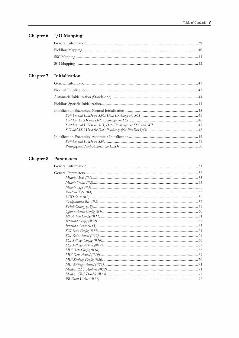
Table of Contents V
Chapter 6 I/O Mapping
General Information .............................................................................................................................. 39
Fieldbus Mapping ................................................................................................................................... 40
SSC Mapping........................................................................................................................................... 41
SCI Mapping ........................................................................................................................................... 42
Chapter 7 Initialization
General Information .............................................................................................................................. 43
Normal Initialization.............................................................................................................................. 43
Automatic Initialization (Standalone).................................................................................................. 44
Fieldbus Specific Initialization.............................................................................................................. 44
Initialization Examples, Normal Initialization ................................................................................... 45Switches and LEDs on SSC, Data Exchange via SCI ................................................................. 45Switches, LEDs and Data Exchange via SCI............................................................................... 46Switches and LEDs on SCI, Data Exchange via SSC and SCI ................................................... 47SCI and SSC Used for Data Exchange (No Fieldbus I/O) ......................................................... 48
Initialization Examples, Automatic Initialization .............................................................................. 49Switches and LEDs on SSC ......................................................................................................... 49Preconfigured Node Address, no LEDs ......................................................................................... 50
Chapter 8 Parameters
General Information .............................................................................................................................. 51
General Parameters ................................................................................................................................ 52Module Mode (#1) ........................................................................................................................ 53Module Status (#2) ....................................................................................................................... 54Module Type (#3) ......................................................................................................................... 55Fieldbus Type (#4)........................................................................................................................ 55LED State (#7) ........................................................................................................................... 56Configuration Bits (#8) ................................................................................................................. 57Switch Coding (#9) ....................................................................................................................... 59Offline Action Config (#10) .......................................................................................................... 60Idle Action Config (#11)............................................................................................................... 61Interrupt Config (#12) .................................................................................................................. 62Interrupt Cause (#13) ................................................................................................................... 63SCI Rate Config (#14) ................................................................................................................. 64SCI Rate Actual (#15) ................................................................................................................ 65SCI Settings Config (#16)............................................................................................................. 66SCI Settings Actual (#17)............................................................................................................ 67MIF Rate Config (#18) ................................................................................................................ 68MIF Rate Actual (#19) ............................................................................................................... 69MIF Settings Config (#20) ........................................................................................................... 70MIF Settings Actual (#21)........................................................................................................... 71Modbus RTU Address (#22) ....................................................................................................... 71Modbus CRC Disable (#23) ........................................................................................................ 72FB Fault Values (#27) ................................................................................................................ 72
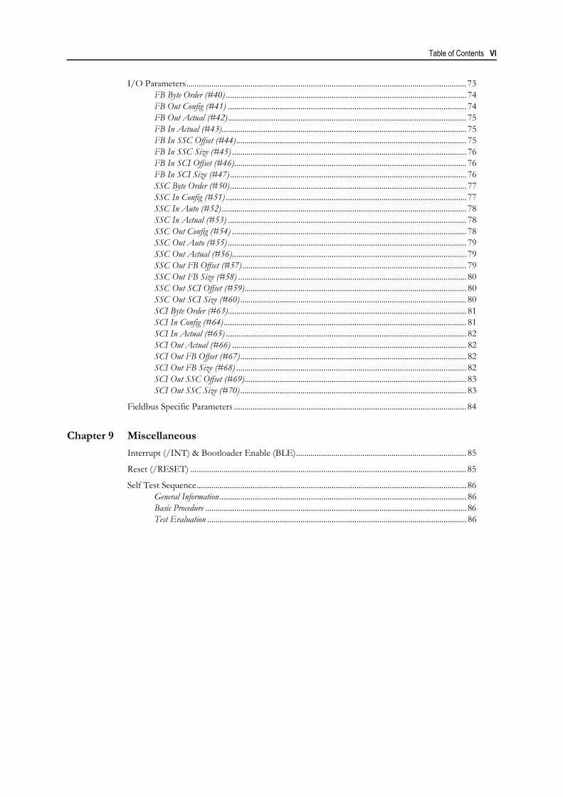
Table of Contents VI
I/O Parameters....................................................................................................................................... 73FB Byte Order (#40) .................................................................................................................... 74FB Out Config (#41) ................................................................................................................... 74FB Out Actual (#42)................................................................................................................... 75FB In Actual (#43)...................................................................................................................... 75FB In SSC Offset (#44)............................................................................................................... 75FB In SSC Size (#45) ................................................................................................................. 76FB In SCI Offset (#46)................................................................................................................ 76FB In SCI Size (#47) .................................................................................................................. 76SSC Byte Order (#50).................................................................................................................. 77SSC In Config (#51) .................................................................................................................... 77SSC In Auto (#52) ...................................................................................................................... 78SSC In Actual (#53) ................................................................................................................... 78SSC Out Config (#54) ................................................................................................................. 78SSC Out Auto (#55) ................................................................................................................... 79SSC Out Actual (#56)................................................................................................................. 79SSC Out FB Offset (#57) ............................................................................................................ 79SSC Out FB Size (#58) .............................................................................................................. 80SSC Out SCI Offset (#59)........................................................................................................... 80SSC Out SCI Size (#60) ............................................................................................................. 80SCI Byte Order (#63)................................................................................................................... 81SCI In Config (#64)..................................................................................................................... 81SCI In Actual (#65) .................................................................................................................... 82SCI Out Actual (#66) ................................................................................................................. 82SCI Out FB Offset (#67)............................................................................................................. 82SCI Out FB Size (#68) ............................................................................................................... 82SCI Out SSC Offset (#69)........................................................................................................... 83SCI Out SSC Size (#70) ............................................................................................................. 83
Fieldbus Specific Parameters ................................................................................................................ 84
Chapter 9 Miscellaneous
Interrupt (/INT) & Bootloader Enable (BLE).................................................................................. 85
Reset (/RESET) ..................................................................................................................................... 85
Self Test Sequence.................................................................................................................................. 86General Information ....................................................................................................................... 86Basic Procedure .............................................................................................................................. 86Test Evaluation ............................................................................................................................. 86
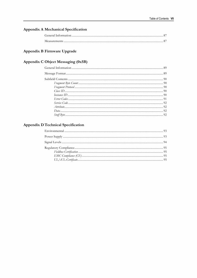
Table of Contents VII
Appendix A Mechanical Specification
General Information .............................................................................................................................. 87
Measurements ......................................................................................................................................... 87
Appendix B Firmware Upgrade
Appendix C Object Messaging (0x5B)
General Information .............................................................................................................................. 89
Message Format...................................................................................................................................... 89
Subfield Contents ................................................................................................................................... 90Fragment Byte Count ..................................................................................................................... 90Fragment Protocol .......................................................................................................................... 90Class ID........................................................................................................................................ 90Instance ID.................................................................................................................................... 90Error Codes ................................................................................................................................... 91Service Code ................................................................................................................................... 92Attribute........................................................................................................................................ 92Data .............................................................................................................................................. 92Stuff Byte ....................................................................................................................................... 92
Appendix D Technical Specification
Environmental ........................................................................................................................................ 93
Power Supply .......................................................................................................................................... 93
Signal Levels ............................................................................................................................................ 94
Regulatory Compliance.......................................................................................................................... 95Fieldbus Certification ..................................................................................................................... 95EMC Compliance (CE) ................................................................................................................ 95UL/cUL-Certificate...................................................................................................................... 95

Doc.Id. HMSI-168-7Anybus-IC Design GuideDoc.Rev. 2.01
Preface
P. About This Document
For more information, documentation etc., please visit the HMS website, ‘www.anybus.com’.
P.1 Related Documents
Document Author
Anybus-IC Profibus DP Appendix HMS
Anybus-IC DeviceNet Appendix HMS
Anybus-IC EtherNet/IP Appendix HMS
Anybus-IC Profinet IO Appendix HMS
Anybus-IC CANopen Appendix HMS
Modbus Protocol Reference Guide Modicon
- -
Preface 9
Doc.Id. HMSI-168-7Anybus-IC Design GuideDoc.Rev. 2.01
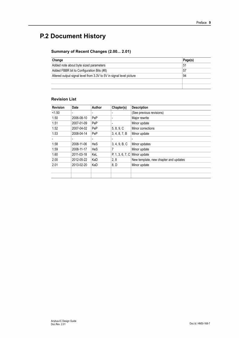
P.2 Document History
Summary of Recent Changes (2.00... 2.01)
Revision List
Change Page(s)
Added note about byte sized parameters 51
Added FBBR bit to Configuration Bits (#8) 57
Altered output signal level from 3.3V to 5V in signal level picture 94
Revision Date Author Chapter(s) Description
<1.50 - - - (See previous revisions)
1.50 2006-08-10 PeP - Major rewrite
1.51 2007-01-09 PeP - Minor update
1.52 2007-04-02 PeP 5, 8, 9, C Minor corrections
1.53 2008-04-14 PeP 3, 4, 8, 7, B Minor update
- - - - -
1.58 2008-11-06 HeS 3, 4, 9, B, C Minor updates
1.59 2008-11-17 HeS 7 Minor update
1.60 2011-03-18 KeL P, 1, 3, 6, 7, C Minor update
2.00 2012-05-22 KaD 2, 8 New template, new chapter and updates
2.01 2013-02-20 KaD 8, D Minor update
Preface 10
Doc.Id. HMSI-168-7Anybus-IC Design GuideDoc.Rev. 2.01
P.3 Document Conventions
The following conventions are used throughout this manual:
• Numbered lists provide sequential steps
• Bulleted lists provide information, not procedural steps
• The term ‘Anybus’ or ‘module’ is used when referring to the Anybus-IC.
• The terms ‘application’ is used when referring to the hardware that hosts the Anybus-IC
• Hexadecimal values are written in the format 0xNNNN, where NNNN is the hexadecimal value.
• Measurements expressed in this document have a tolerance of ±0.20 mm unless otherwise stated.
• Signals which are “pulled to NN” are connected to NN via a resistor.
• Signals which are “tied to NN” are directly connected to NN.
• Modbus register numbers are specified using the protocol convention (base 0), i.e. there is a 1:1 correlation between the register number specified in this document and the actual register value in the message frame.
Preface 11
Doc.Id. HMSI-168-7Anybus-IC Design GuideDoc.Rev. 2.01
P.4 Sales and Support
Sales Support
HMS Sweden (Head Office)
E-mail: [email protected] E-mail: [email protected]
Phone: +46 (0) 35 - 17 29 56 Phone: +46 (0) 35 - 17 29 20
Fax: +46 (0) 35 - 17 29 09 Fax: +46 (0) 35 - 17 29 09
Online: www.anybus.com Online: www.anybus.com
HMS North America
E-mail: [email protected] E-mail: [email protected]
Phone: +1-312 - 829 - 0601 Phone: +1-312-829-0601
Toll Free: +1-888-8-Anybus Toll Free: +1-888-8-Anybus
Fax: +1-312-629-2869 Fax: +1-312-629-2869
Online: www.anybus.com Online: www.anybus.com
HMS Germany
E-mail: [email protected] E-mail: [email protected]
Phone: +49 (0) 721-989777-000 Phone: +49 (0) 721-989777-000
Fax: +49 (0) 721-989777-010 Fax: +49 (0) 721-989777-010
Online: www.anybus.de Online: www.anybus.de
HMS Japan
E-mail: [email protected] E-mail: [email protected]
Phone: +81 (0) 45-478-5340 Phone: +81 (0) 45-478-5340
Fax: +81 (0) 45-476-0315 Fax: +81 (0) 45-476-0315
Online: www.anybus.jp Online: www.anybus.jp
HMS China
E-mail: [email protected] E-mail: [email protected]
Phone: +86 (0) 10-8532-3183 Phone: +86 (0) 10-8532-3023
Fax: +86 (0) 10-8532-3209 Fax: +86 (0) 10-8532-3209
Online: www.anybus.cn Online: www.anybus.cn
HMS Italy
E-mail: [email protected] E-mail: [email protected]
Phone: +39 039 59662 27 Phone: +39 039 59662 27
Fax: +39 039 59662 31 Fax: +39 039 59662 31
Online: www.anybus.it Online: www.anybus.it
HMS France
E-mail: [email protected] E-mail: [email protected]
Phone: +33 (0) 3 68 368 034 Phone: +33 (0) 3 68 368 033
Fax: +33 (0) 3 68 368 031 Fax: +33 (0) 3 68 368 031
Online: www.anybus.fr Online: www.anybus.fr
HMS UK & Eire
E-mail: [email protected] E-mail: [email protected]
Phone: +44 (0) 1926 405599 Phone: +46 (0) 35 - 17 29 20
Fax: +44 (0) 1926 405522 Fax: +46 (0) 35 - 17 29 09
Online: www.anybus.co.uk Online: www.anybus.com
HMS Denmark
E-mail: [email protected] E-mail: [email protected]
Phone: +45 (0) 35 38 29 00 Phone: +46 (0) 35 - 17 29 20
Fax: +46 (0) 35 17 29 09 Fax: +46 (0) 35 - 17 29 09
Online: www.anybus.com Online: www.anybus.com
HMS India
E-mail: [email protected] E-mail: [email protected]
Phone: +91 (0) 20 40111201 Phone: +91 (0) 20 40111201
Fax: +91 (0) 20 40111105 Fax: +91 (0) 20 40111105
Online: www.anybus.com Online: www.anybus.com
Doc.Id. HMSI-168-7Anybus-IC Design GuideDoc.Rev. 2.01
Chapter 1
1. About the Anybus-IC
1.1 General
The Anybus-IC network communication module is a high performance, low cost communication solu-tion for industrial field devices. Typical applications include I/O blocks, temperature controllers, meas-uring devices, and other devices where size is an issue.
A flexible application interface enables the module to operate either standalone or controlled by a mi-crocontroller. A range of communication channels allows fieldbus data exchange as well as internal dis-crete I/O. In addition, data can be mapped between the various channels in a flexible manner without any intervention by the host system.
The Anybus-IC software interface is designed to be network protocol independent, making it possible to support several networking systems using the same software driver. The host communication is based on Modbus RTU, a proven protocol which is easy to implement yet flexible enough to provide room for future expansion. This also allows for multidrop configurations where multiple Anybus-IC modules are interfaced to the same microcontroller.
1.2 Features
• Standard 32-pin dual in line footprint
• Requires only a single 5 V power supply
• Galvanically isolated fieldbus electronics
• Serial Communications Interface (SCI)
• Synchronous Serial Channel (SSC)
• Text based configuration- and monitoring interface (MIF)
• Up to 144 bytes of fieldbus I/O in each direction
• Up to 128 bytes of serial I/O in each direction (SCI)
• Up to 128 bits of I/O in each direction (SSC)
• Flexible mapping of data
• Standalone or microcontroller operation
Chapter 1 13
Doc.Id. HMSI-168-7Anybus-IC Design GuideDoc.Rev. 2.01
1.3 Overview
Internals
The figure below illustrates the basic properties of the Anybus-IC, on-board I/O, fieldbus interface etc.
Data Mapping
The module features a flexible data mapping scheme; data received on one communication channel can be mapped (i.e copied) to the other, and vice versa. This allows for not just fieldbus connectivity, but also for internal I/O in the application, by mapping SSC I/O to the SCI channel. By mapping fieldbus I/O to the SSC channel, SSC I/O can be accessed directly from the fieldbus.
Physical Network Layer
Isolation
Fieldbus Control
CPU Memory
Flash
SCI Tx Rx DE
SSC Dout Din1 Din2 LD CLK
MIF Tx Rx
Fieldbus
SSC
SCI
From FieldbusControl System
DigitalInputs
(Shift registers)
ApplicationIntelligence
(Microcontroller)
ApplicationIntelligence
(Microcontroller)
To FieldbusControl System
DigitalOutputs
(Shift registers)SSC
SCI
Fieldbus
Chapter 1 14
Doc.Id. HMSI-168-7Anybus-IC Design GuideDoc.Rev. 2.01
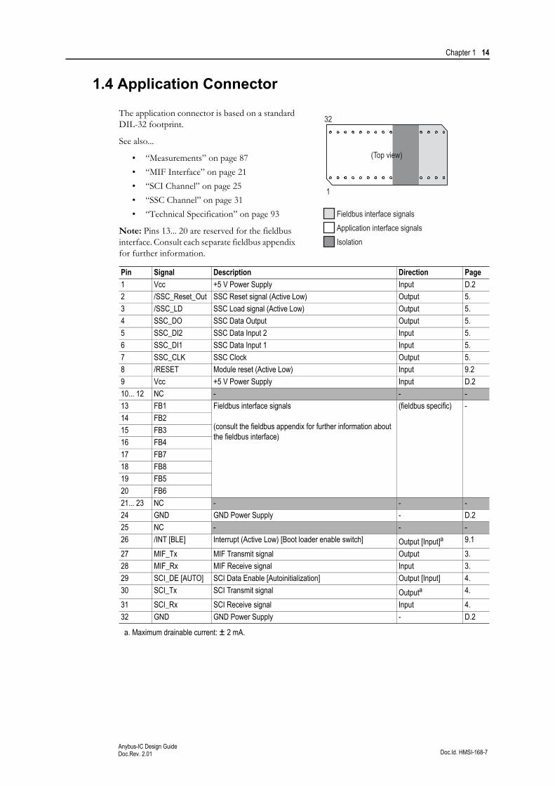
1.4 Application Connector
The application connector is based on a standard DIL-32 footprint.
See also...
• “Measurements” on page 87
• “MIF Interface” on page 21
• “SCI Channel” on page 25
• “SSC Channel” on page 31
• “Technical Specification” on page 93
Note: Pins 13... 20 are reserved for the fieldbus interface. Consult each separate fieldbus appendix for further information.
Pin Signal Description Direction Page
1 Vcc +5 V Power Supply Input D.2
2 /SSC_Reset_Out SSC Reset signal (Active Low) Output 5.
3 /SSC_LD SSC Load signal (Active Low) Output 5.
4 SSC_DO SSC Data Output Output 5.
5 SSC_DI2 SSC Data Input 2 Input 5.
6 SSC_DI1 SSC Data Input 1 Input 5.
7 SSC_CLK SSC Clock Output 5.
8 /RESET Module reset (Active Low) Input 9.2
9 Vcc +5 V Power Supply Input D.2
10... 12 NC - - -
13 FB1 Fieldbus interface signals
(consult the fieldbus appendix for further information about the fieldbus interface)
(fieldbus specific) -
14 FB2
15 FB3
16 FB4
17 FB7
18 FB8
19 FB5
20 FB6
21... 23 NC - - -
24 GND GND Power Supply - D.2
25 NC - - -
26 /INT [BLE] Interrupt (Active Low) [Boot loader enable switch] Output [Input]a
a. Maximum drainable current: ± 2 mA.
9.1
27 MIF_Tx MIF Transmit signal Output 3.
28 MIF_Rx MIF Receive signal Input 3.
29 SCI_DE [AUTO] SCI Data Enable [Autoinitialization] Output [Input] 4.
30 SCI_Tx SCI Transmit signal Outputa 4.
31 SCI_Rx SCI Receive signal Input 4.
32 GND GND Power Supply - D.2
(Top view)
1
32
Fieldbus interface signalsApplication interface signalsIsolation
Doc.Id. HMSI-168-7Anybus-IC Design GuideDoc.Rev. 2.01
Chapter 2
2. Tutorial
2.1 Introduction
This tutorial will describe how to map data between the three different communication channels (Field-bus, SSC, SCI) and how to communicate with the Anybus-IC using the SCI interface and a Modbus mas-ter. It is assumed that the Anybus-IC is socketed and ready, and that all pins and connectors are connected and ready for use.
The Anybus-IC has three possible modes of operation. For a detailed description of each operation mode, see “Initialization” on page 43. This tutorial will describe how to set up normal mode communi-cation, e.g. where the module shall be controlled by a microcontroller via the SCI channel.
As said above, the Anybus-IC features three possible communication channels:
• SSC (Synchronous Serial Channel)
Data to and from the digital outputs/inputs of the application, e.g. LEDs and switches.
• SCI (Serial Communications Interface)
Data coming from and going to the Modbus master of the host application.
• FB (Fieldbus)
Data coming from and going to the fieldbus side of the application. Data from the fieldbus to the Anybus-IC is called FB OUT, and data from the Anybus-IC to the fieldbus is called FB IN.
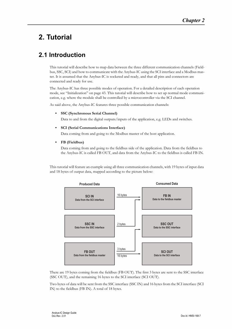
This tutorial will feature an example using all three communication channels, with 19 bytes of input data and 18 bytes of output data, mapped according to the picture below:
There are 19 bytes coming from the fieldbus (FB OUT). The first 3 bytes are sent to the SSC interface (SSC OUT), and the remaining 16 bytes to the SCI interface (SCI OUT).
Two bytes of data will be sent from the SSC interface (SSC IN) and 16 bytes from the SCI interface (SCI IN) to the fieldbus (FB IN). A total of 18 bytes.
SCI INData from the SCI interface
FB INData to the fieldbus master
SSC OUTData to the SSC interface
Produced Data Consumed Data
SSC INData from the SSC interface
FB OUTData from the fieldbus master
SCI OUTData to the SCI interface
16 bytes
2 bytes
3 bytes
16 bytes
Chapter 2 16
Doc.Id. HMSI-168-7Anybus-IC Design GuideDoc.Rev. 2.01
2.2 Step by Step Guide
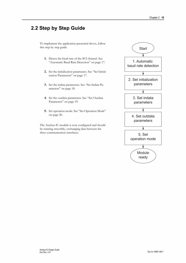
To implement the application presented above, follow this step by step guide.
1. Detect the baud rate of the SCI channel. See “Automatic Baud Rate Detection” on page 17.
2. Set the initialization parameters. See “Set Initial-ization Parameters” on page 17.
3. Set the indata parameters. See “Set Indata Pa-rameters” on page 18.
4. Set the outdata parameters. See “Set Outdata Parameters” on page 19.
5. Set operation mode. See “Set Operation Mode” on page 20.
The Anybus-IC module is now configured and should be running smoothly, exchanging data between the three communication interfaces.
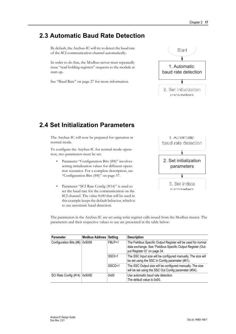
1. Automatic
baud rate detection
2. Set initialization
parameters
3. Set indata
parameters
4. Set outdata
parameters
5. Set
operation mode
Start
Module
ready
Chapter 2 17
Doc.Id. HMSI-168-7Anybus-IC Design GuideDoc.Rev. 2.01
2.3 Automatic Baud Rate Detection
By default, the Anybus-IC will try to detect the baud rate of the SCI communication channel automatically.
In order to do that, the Modbus server must repeatedly issue “read holding registers”-requests to the module at start-up.
See “Baud Rate” on page 27 for more information.
2.4 Set Initialization Parameters
The Anybus-IC will now be prepared for operation in normal mode.
To configure the Anybus-IC for normal mode opera-tion, two parameters must be set.
• Parameter “Configuration Bits (#8)” involves setting initialization values for different opera-tion scenarios. For a complete description, see “Configuration Bits (#8)” on page 57.
• Parameter “SCI Rate Config (#14)” is used to set the baud rate for the communication on the SCI channel. The value 0x00 that will be used in this example keeps the default behavior, which is to use automatic baud detection.
The parameters in the Anybus-IC are set using write register calls issued from the Modbus master. The parameters and their respective values to use are presented in the table below:
Parameter Modbus Address Setting Description
Configuration Bits (#8) 0x5008 FBLP=1 The Fieldbus Specific Output Register will be used for normal data exchange. See “Fieldbus Specific Output Register (Out-put Register 0)” on page 34.
SSCI=1 The SSC Input size will be configured manually. The size will be set using the SSC In Config parameter (#51).
SSCO=1 The SSC Output size will be configured manually. The size will be set using the SSC Out Config parameter (#54).
SCI Rate Config (#14) 0x500E 0x00 Use automatic baud rate detection. The default value is 0x00.
1. Automatic
baud rate detection
2. Set initialization
parameters
Start
1. Automatic
baud rate detection
2. Set initialization
parameters
3. Set indata
parameters
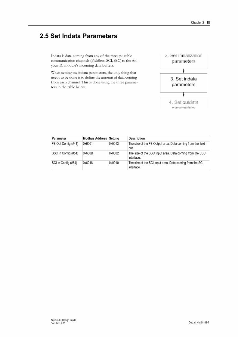
Chapter 2 18
Doc.Id. HMSI-168-7Anybus-IC Design GuideDoc.Rev. 2.01
2.5 Set Indata Parameters
Indata is data coming from any of the three possible communication channels (Fieldbus, SCI, SSC) to the An-ybus-IC module’s incoming data buffers.
When setting the indata parameters, the only thing that needs to be done is to define the amount of data coming from each channel. This is done using the three parame-ters in the table below.
Parameter Modbus Address Setting Description
FB Out Config (#41) 0x6001 0x0013 The size of the FB Output area. Data coming from the field-bus.
SSC In Config (#51) 0x600B 0x0002 The size of the SSC Input area. Data coming from the SSC interface.
SCI In Config (#64) 0x6018 0x0010 The size of the SCI Input area. Data coming from the SCI interface.
2. Set initialization
parameters
3. Set indata
parameters
4. Set outdata
parameters
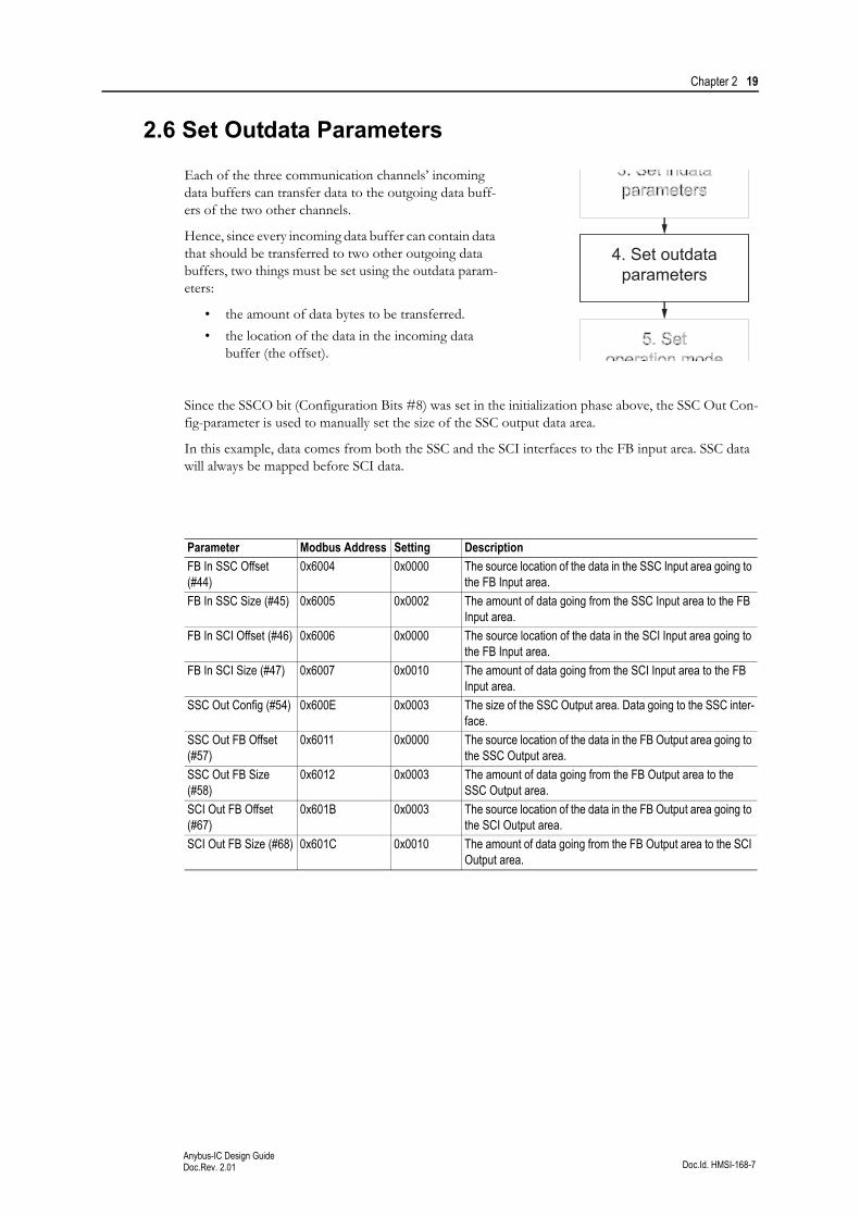
Chapter 2 19
Doc.Id. HMSI-168-7Anybus-IC Design GuideDoc.Rev. 2.01
2.6 Set Outdata Parameters
Each of the three communication channels’ incoming data buffers can transfer data to the outgoing data buff-ers of the two other channels.
Hence, since every incoming data buffer can contain data that should be transferred to two other outgoing data buffers, two things must be set using the outdata param-eters:
• the amount of data bytes to be transferred.
• the location of the data in the incoming data buffer (the offset).
Since the SSCO bit (Configuration Bits #8) was set in the initialization phase above, the SSC Out Con-fig-parameter is used to manually set the size of the SSC output data area.
In this example, data comes from both the SSC and the SCI interfaces to the FB input area. SSC data will always be mapped before SCI data.
Parameter Modbus Address Setting Description
FB In SSC Offset (#44)
0x6004 0x0000 The source location of the data in the SSC Input area going to the FB Input area.
FB In SSC Size (#45) 0x6005 0x0002 The amount of data going from the SSC Input area to the FB Input area.
FB In SCI Offset (#46) 0x6006 0x0000 The source location of the data in the SCI Input area going to the FB Input area.
FB In SCI Size (#47) 0x6007 0x0010 The amount of data going from the SCI Input area to the FB Input area.
SSC Out Config (#54) 0x600E 0x0003 The size of the SSC Output area. Data going to the SSC inter-face.
SSC Out FB Offset (#57)
0x6011 0x0000 The source location of the data in the FB Output area going to the SSC Output area.
SSC Out FB Size (#58)
0x6012 0x0003 The amount of data going from the FB Output area to the SSC Output area.
SCI Out FB Offset (#67)
0x601B 0x0003 The source location of the data in the FB Output area going to the SCI Output area.
SCI Out FB Size (#68) 0x601C 0x0010 The amount of data going from the FB Output area to the SCI Output area.
3. Set indata
parameters
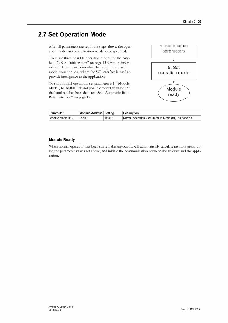
4. Set outdata
parameters
5. Set
operation mode
Chapter 2 20
Doc.Id. HMSI-168-7Anybus-IC Design GuideDoc.Rev. 2.01
2.7 Set Operation Mode
After all parameters are set in the steps above, the oper-ation mode for the application needs to be specified.
There are three possible operation modes for the Any-bus-IC. See “Initialization” on page 43 for more infor-mation. This tutorial describes the setup for normal mode operation, e.g. where the SCI interface is used to provide intelligence to the application.
To start normal operation, set parameter #1 (“Module Mode”) to 0x0001. It is not possible to set this value until the baud rate has been detected. See “Automatic Baud Rate Detection” on page 17.
Module Ready
When normal operation has been started, the Anybus-IC will automatically calculate memory areas, us-ing the parameter values set above, and initiate the communication between the fieldbus and the appli-cation.
Parameter Modbus Address Setting Description
Module Mode (#1) 0x5001 0x0001 Normal operation. See “Module Mode (#1)” on page 53.
4. Set outdata
parameters
5. Set
operation mode
Module
ready
Doc.Id. HMSI-168-7Anybus-IC Design GuideDoc.Rev. 2.01
Chapter 3
3. MIF Interface
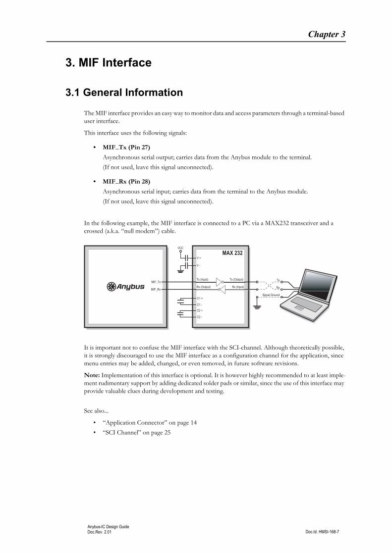
3.1 General Information
The MIF interface provides an easy way to monitor data and access parameters through a terminal-based user interface.
This interface uses the following signals:
• MIF_Tx (Pin 27)
Asynchronous serial output; carries data from the Anybus module to the terminal.
(If not used, leave this signal unconnected).
• MIF_Rx (Pin 28)
Asynchronous serial input; carries data from the terminal to the Anybus module.
(If not used, leave this signal unconnected).
In the following example, the MIF interface is connected to a PC via a MAX232 transceiver and a crossed (a.k.a. “null modem”) cable.
It is important not to confuse the MIF interface with the SCI-channel. Although theoretically possible, it is strongly discouraged to use the MIF interface as a configuration channel for the application, since menu entries may be added, changed, or even removed, in future software revisions.
Note: Implementation of this interface is optional. It is however highly recommended to at least imple-ment rudimentary support by adding dedicated solder pads or similar, since the use of this interface may provide valuable clues during development and testing.
See also...
• “Application Connector” on page 14
• “SCI Channel” on page 25
Tx (Input)
Rx (Output)
Tx (Output)
Rx (Input)
V +
V -
MAX 232
C1 +
C1 - C2 +
C2 -
VCC
MIF_Tx
MIF_RxSignal Ground
Rx
Tx
Chapter 3 22
Doc.Id. HMSI-168-7Anybus-IC Design GuideDoc.Rev. 2.01
3.2 Communication Settings
3.2.1 Baud rate
The MIF interface supports baud rates from 4.8 kbps to 57.6 kbps (default is 38.4 kbps). Unlike the SCI interface, automatic baud rate detection is not supported.
See also...
• “MIF Rate Config (#18)” on page 68
• “MIF Rate Actual (#19)” on page 69
3.2.2 Communication Properties
The interface supports 1 or 2 stop bits, none, odd or even parity. Default is 1 stop bit, no parity. The number of data bits is fixed to 8.
See also...
• “MIF Settings Config (#20)” on page 70
• “MIF Settings Actual (#21)” on page 71
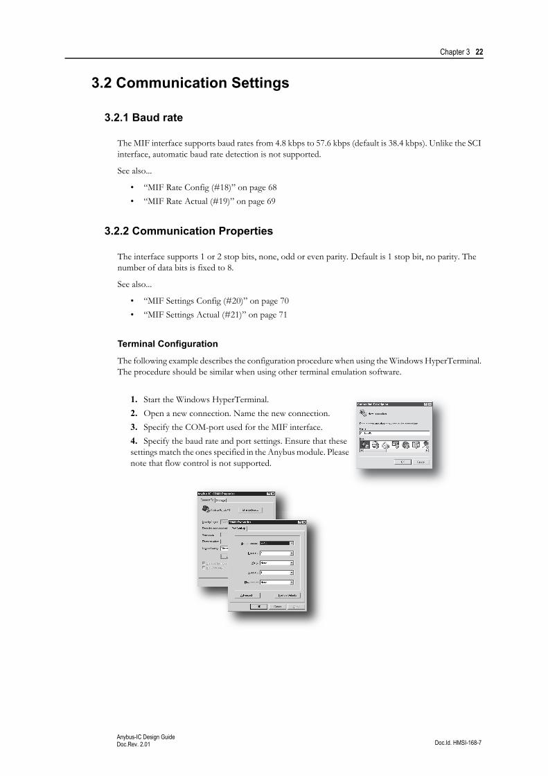
Terminal Configuration
The following example describes the configuration procedure when using the Windows HyperTerminal. The procedure should be similar when using other terminal emulation software.
1. Start the Windows HyperTerminal.
2. Open a new connection. Name the new connection.
3. Specify the COM-port used for the MIF interface.
4. Specify the baud rate and port settings. Ensure that these settings match the ones specified in the Anybus module. Please note that flow control is not supported.
Chapter 3 23
Doc.Id. HMSI-168-7Anybus-IC Design GuideDoc.Rev. 2.01
3.3 User Interface
3.3.1 General Information
The MIF interface features a menu-based user interface as follows:
• To enter a submenu or parameter, type the corresponding digit and press <Enter>.
• To enter a parameter value, enter the value and press <Enter>.
• To return to a previous menu, or cancel a parameter input, press <ESC>.
• To redraw the current menu, press <Enter>.
3.3.2 Main Menu
The main menu provides access to the various submenus. It also displays the fieldbus type.
------------------------------------------ Anybus-IC - Main Menu Profibus-DP------------------------------------------ 1 - Module Information 2 - Parameters 3 - Monitor 4 - Firmware Upgrade------------------------------------------>
See also...
• “‘Module Information’-menu” on page 23
• “‘Parameters’-menu” on page 24
• “‘Monitor’-menu” on page 24
• “‘Firmware Upgrade’-menu” on page 24
3.3.3 ‘Module Information’-menu
This menu features two additional submenus; ‘Software Versions’, which provides information about the current Anybus-IC firmware, and ‘Product Information’, which provides manufacturing information such as serial number and production date.
------------------------------------------ Anybus-IC - Information------------------------------------------ 1 - Software Versions 2 - Product Information------------------------------------------>
Chapter 3 24
Doc.Id. HMSI-168-7Anybus-IC Design GuideDoc.Rev. 2.01
3.3.4 ‘Parameters’-menu
This menu provides access to all parameters in the module.
------------------------------------------Anybus-IC - Parameters------------------------------------------ 1 - Anybus-IC 2 - FB I/O Settings 3 - SSC I/O Settings 4 - SCI I/O Settings 5 - Fieldbus Specific------------------------------------------>
See also...
• “Register Map” on page 26
• “Parameters” on page 51
3.3.5 ‘Monitor’-menu
All active I/O buffers can be monitored in this menu.
------------------------------------------ Anybus-IC - I/O Areas------------------------------------------ 1 - Fieldbus Out 2 - SSC In 3 - SCI In 4 - Fieldbus In 5 - SSC Out 6 - SCI Out------------------------------------------>
Example:
Monitoring of ‘Fieldbus In’-area (submenu #4):
-------------------------------- Anybus-IC - Fieldbus In-------------------------------- Byte # 0 1100 0011 0xc3 1 0000 0000 0x00-------------------------------->
Note: The information is not refreshed automatically. Press <Enter> to update the screen.
See also...
• “SCI Channel” on page 25
• “SSC Channel” on page 31
3.3.6 ‘Firmware Upgrade’-menu
This menu is used when upgrading the firmware of the module.
See also “Firmware Upgrade” on page 88.
Doc.Id. HMSI-168-7Anybus-IC Design GuideDoc.Rev. 2.01
Chapter 4
4. SCI Channel
4.1 General Information
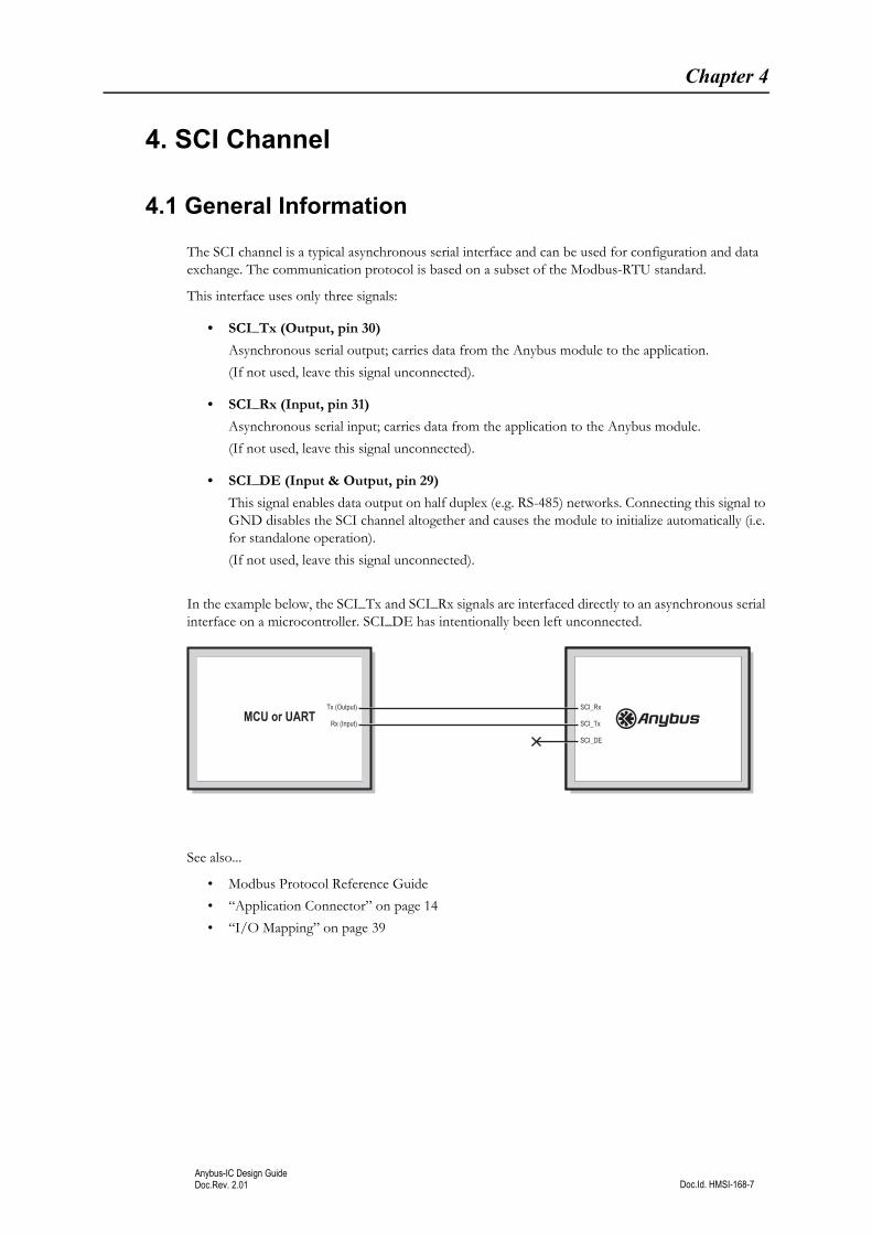
The SCI channel is a typical asynchronous serial interface and can be used for configuration and data exchange. The communication protocol is based on a subset of the Modbus-RTU standard.
This interface uses only three signals:
• SCI_Tx (Output, pin 30)
Asynchronous serial output; carries data from the Anybus module to the application.
(If not used, leave this signal unconnected).
• SCI_Rx (Input, pin 31)
Asynchronous serial input; carries data from the application to the Anybus module.
(If not used, leave this signal unconnected).
• SCI_DE (Input & Output, pin 29)
This signal enables data output on half duplex (e.g. RS-485) networks. Connecting this signal to GND disables the SCI channel altogether and causes the module to initialize automatically (i.e. for standalone operation).
(If not used, leave this signal unconnected).
In the example below, the SCI_Tx and SCI_Rx signals are interfaced directly to an asynchronous serial interface on a microcontroller. SCI_DE has intentionally been left unconnected.
See also...
• Modbus Protocol Reference Guide
• “Application Connector” on page 14
• “I/O Mapping” on page 39
Tx (Output)
Rx (Input)MCU or UART
SCI_Rx
SCI_Tx
SCI_DE
Chapter 4 26
Doc.Id. HMSI-168-7Anybus-IC Design GuideDoc.Rev. 2.01
4.2 Modbus Implementation
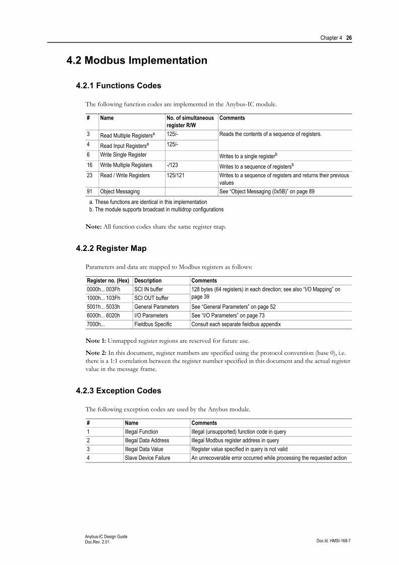
4.2.1 Functions Codes
The following function codes are implemented in the Anybus-IC module.
Note: All function codes share the same register map.
4.2.2 Register Map
Parameters and data are mapped to Modbus registers as follows:
Note 1: Unmapped register regions are reserved for future use.
Note 2: In this document, register numbers are specified using the protocol convention (base 0), i.e. there is a 1:1 correlation between the register number specified in this document and the actual register value in the message frame.
4.2.3 Exception Codes
The following exception codes are used by the Anybus module.
# Name No. of simultaneous register R/W
Comments
3 Read Multiple Registersa
a. These functions are identical in this implementation
125/- Reads the contents of a sequence of registers.
4 Read Input Registersa 125/-
6 Write Single Register Writes to a single registerb
b. The module supports broadcast in multidrop configurations
16 Write Multiple Registers -/123 Writes to a sequence of registersb
23 Read / Write Registers 125/121 Writes to a sequence of registers and returns their previous values
91 Object Messaging See “Object Messaging (0x5B)” on page 89
Register no. (Hex) Description Comments
0000h... 003Fh SCI IN buffer 128 bytes (64 registers) in each direction; see also “I/O Mapping” on page 391000h... 103Fh SCI OUT buffer
5001h... 5033h General Parameters See “General Parameters” on page 52
6000h... 6020h I/O Parameters See “I/O Parameters” on page 73
7000h... Fieldbus Specific Consult each separate fieldbus appendix
# Name Comments
1 Illegal Function Illegal (unsupported) function code in query
2 Illegal Data Address Illegal Modbus register address in query
3 Illegal Data Value Register value specified in query is not valid
4 Slave Device Failure An unrecoverable error occurred while processing the requested action
Chapter 4 27
Doc.Id. HMSI-168-7Anybus-IC Design GuideDoc.Rev. 2.01
4.3 Communication Settings
4.3.1 Baud Rate
The SCI channel supports baud rates from 4.8 kbps to 57.6 kbps. By de-fault, the module attempts to detect the baud rate automatically. This is not part of the Modbus RTU specification, and requires a special startup sequence (see flowchart).
• During start-up, the application must repeatedly issue ‘Read Holding Registers’-requests to slave address 0x01. Wait at least 10 ms before reissuing the request.
Example: read data from Modbus register 0x5001 by issuing “01h 03h 50h 01h 00h 01h C4h CAh”.
• The module responds when the correct baud rate has been es-tablished.
• Generally the module detects the baud rate within 20 attempts.
• In order for this functionality to work, the module must be con-figured to use slave address 0x01. This means that it is not pos-sible to use automatic baud rate detection in multidrop systems.
Note: Some Anybus IC modules support further baud rates. Please see “SCI Rate Config (#14)” on page 64”.
See also...
• “SCI Rate Actual (#15)” on page 65
4.3.2 Timeout
Under normal circumstances the Anybus-IC module will start to send a response within 50 ms of the receipt of a correct message. This time should be considered as a minimum timeout value.
4.3.3 Communication Properties
The number of data bits on the SCI channel is fixed to 8. The number of stop bits depends on the parity setting, which is accessed through parameter #16. Flow control is not supported.
Default settings are no parity / 2 stop bits.
See also...
• “SCI Settings Config (#16)” on page 66
• “SCI Settings Actual (#17)” on page 67
Note: If using automatic baud rate detection, these settings are detected by the module automatically.
Send ‘Read Multiple Registers’
in intervals of at least 10 ms
Start
Check for response
Did the module
send a valid response?
Baud rate detected
Yes
No

Chapter 4 28
Doc.Id. HMSI-168-7Anybus-IC Design GuideDoc.Rev. 2.01
4.3.4 Modbus RTU Address
The communication protocol allows multiple Anybus modules to be interfaced to the same microcon-troller (e.g. using a multi-drop RS-485 network). In such cases, each module must be assigned a unique Modbus RTU address.
See also...
• “Interfacing to RS-485 (Multidrop)” on page 30
• “Modbus RTU Address (#22)” on page 71
Chapter 4 29
Doc.Id. HMSI-168-7Anybus-IC Design GuideDoc.Rev. 2.01
4.4 Interfacing to RS-232
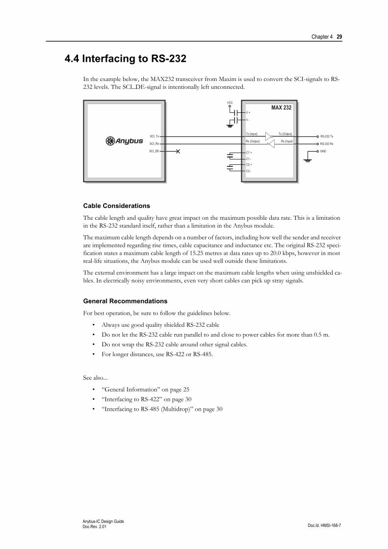
In the example below, the MAX232 transceiver from Maxim is used to convert the SCI-signals to RS-232 levels. The SCI_DE-signal is intentionally left unconnected.
Cable Considerations
The cable length and quality have great impact on the maximum possible data rate. This is a limitation in the RS-232 standard itself, rather than a limitation in the Anybus module.
The maximum cable length depends on a number of factors, including how well the sender and receiver are implemented regarding rise times, cable capacitance and inductance etc. The original RS-232 speci-fication states a maximum cable length of 15.25 metres at data rates up to 20.0 kbps, however in most real-life situations, the Anybus module can be used well outside these limitations.
The external environment has a large impact on the maximum cable lengths when using unshielded ca-bles. In electrically noisy environments, even very short cables can pick up stray signals.
General Recommendations
For best operation, be sure to follow the guidelines below.
• Always use good quality shielded RS-232 cable
• Do not let the RS-232 cable run parallel to and close to power cables for more than 0.5 m.
• Do not wrap the RS-232 cable around other signal cables.
• For longer distances, use RS-422 or RS-485.
See also...
• “General Information” on page 25
• “Interfacing to RS-422” on page 30
• “Interfacing to RS-485 (Multidrop)” on page 30
Tx (Input)
Rx (Output)
Tx (Output)
Rx (Input)
V +
V -
RS-232 Tx
RS-232 Rx
GND
MAX 232
C1 +
C1 - C2 +
C2 -
VCC
SCI_Tx
SCI_Rx
SCI_DE
Chapter 4 30
Doc.Id. HMSI-168-7Anybus-IC Design GuideDoc.Rev. 2.01
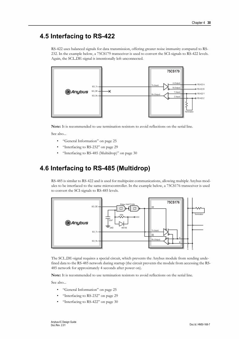
4.5 Interfacing to RS-422
RS-422 uses balanced signals for data transmission, offering greater noise immunity compared to RS-232. In the example below, a 75CS179 transceiver is used to convert the SCI-signals to RS-422 levels. Again, the SCI_DE-signal is intentionally left unconnected.
Note: It is recommended to use termination resistors to avoid reflections on the serial line.
See also...
• “General Information” on page 25
• “Interfacing to RS-232” on page 29
• “Interfacing to RS-485 (Multidrop)” on page 30
4.6 Interfacing to RS-485 (Multidrop)
RS-485 is similar to RS-422 and is used for multipoint communications, allowing multiple Anybus mod-ules to be interfaced to the same microcontroller. In the example below, a 75CS176 transceiver is used to convert the SCI-signals to RS-485 levels.
The SCI_DE-signal requires a special circuit, which prevents the Anybus module from sending unde-fined data to the RS-485 network during startup (the circuit prevents the module from accessing the RS-485 network for approximately 4 seconds after power on).
Note: It is recommended to use termination resistors to avoid reflections on the serial line.
See also...
• “General Information” on page 25
• “Interfacing to RS-232” on page 29
• “Interfacing to RS-422” on page 30
Tx (Input)
Rx (Output)
A (Output)
B (Output)
Y (Input)
Z (Input)
RS-422 A
RS-422 B
RS-422 Y
RS-422 Z
75CS179
Termination
SCI_Tx
SCI_DE
SCI_Rx
Tx (Input)
Rx (Output)
DE
REA
B
75CS176
SCI_Tx
SCI_Rx
SCI_DE
A B
Termination
IN4148
22uF
470kVCC
GND
Philips 74HCT132N
Doc.Id. HMSI-168-7Anybus-IC Design GuideDoc.Rev. 2.01
Chapter 5
5. SSC Channel
5.1 General Information
The SSC channel uses a synchronous serial interface similar to the Motorola SPI, intended for discrete I/O and fieldbus-specific input/output signals such as node address and LED indications.
The Anybus-IC expects that any circuitry that is wired to the SSC is 100% sequence- and timing-com-patible to the chain of 165/594 discrete shift registers mounted on the same circuit board as the module. The application designer using the SSC interface must make sure that their circuitry is, from a sequence and timing viewpoint, identical to a 165/594 shift register chain.
This interface uses 6 signals:
• /SSC_Reset_Out (Pin 2)
Active low signal used to reset the shift registers. The use of this signal is optional.
Note that this signal must not be confused with /RESET (pin 8).
If not used, leave this signal unconnected.
• /SSC_LD (Pin 3)
Shift register load. Loads the value of the shift register inputs on transition to low.
If not used, leave this signal unconnected.
• SSC_DO (Pin 4)
Serial data output. Valid on the falling edge of SSC_CLK.
If not used, leave this signal unconnected.
• SSC_DI2 (Pin 5)
Serial data input 1 from shift registers. Sampled on the rising edge of SSC_CLK.
If not used, leave this signal unconnected.
• SSC_DI1 (Pin 6)
Serial data input 2 from shift registers. Sampled on the rising edge of SSC_CLK.
- If only using Input Registers, connect this signal to SCC_DO.
- If only using Output Registers, connect this signal to SCC_DI2.
- If using both Input- and Output Registers, connect this signal to the serial data line between the Input- and Output Registers.
If not used, leave this signal unconnected.
• SSC_CLK (Pin 7)
Clock output.
If not used, leave this signal unconnected.
See also...
• “Application Connector” on page 14
• “I/O Mapping” on page 39
Chapter 5 32
Doc.Id. HMSI-168-7Anybus-IC Design GuideDoc.Rev. 2.01
5.2 The Shift Register Loop
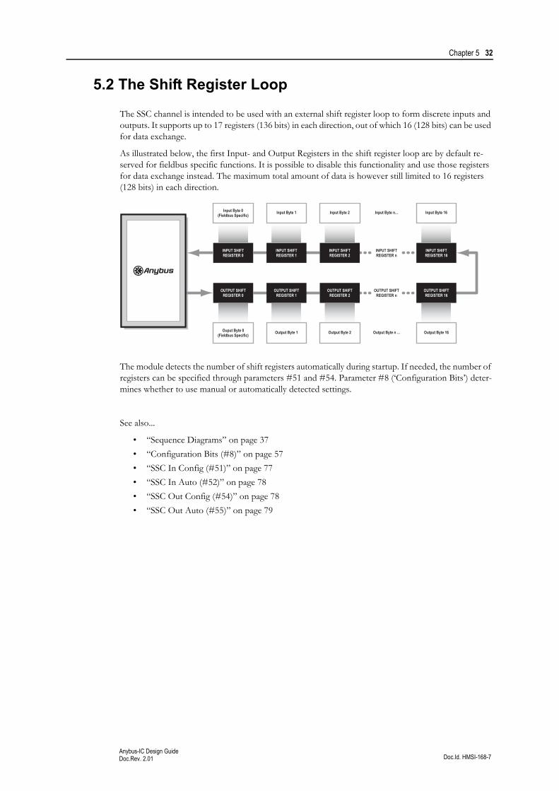
The SSC channel is intended to be used with an external shift register loop to form discrete inputs and outputs. It supports up to 17 registers (136 bits) in each direction, out of which 16 (128 bits) can be used for data exchange.
As illustrated below, the first Input- and Output Registers in the shift register loop are by default re-served for fieldbus specific functions. It is possible to disable this functionality and use those registers for data exchange instead. The maximum total amount of data is however still limited to 16 registers (128 bits) in each direction.
The module detects the number of shift registers automatically during startup. If needed, the number of registers can be specified through parameters #51 and #54. Parameter #8 (‘Configuration Bits’) deter-mines whether to use manual or automatically detected settings.
See also...
• “Sequence Diagrams” on page 37
• “Configuration Bits (#8)” on page 57
• “SSC In Config (#51)” on page 77
• “SSC In Auto (#52)” on page 78
• “SSC Out Config (#54)” on page 78
• “SSC Out Auto (#55)” on page 79
INPUT SHIFTREGISTER 16
Input Byte 16Input Byte n...
Output Byte 16Output Byte n ...
OUTPUT SHIFTREGISTER 16
INPUT SHIFTREGISTER 0
INPUT SHIFTREGISTER 1
INPUT SHIFTREGISTER 2
OUTPUT SHIFTREGISTER 0
OUTPUT SHIFTREGISTER 1
OUTPUT SHIFTREGISTER 2
INPUT SHIFTREGISTER n
Input Byte 0(Fieldbus Specific) Input Byte 1 Input Byte 2
Ouput Byte 0(Fieldbus Specific) Output Byte 1 Output Byte 2
OUTPUT SHIFTREGISTER n
Chapter 5 33
Doc.Id. HMSI-168-7Anybus-IC Design GuideDoc.Rev. 2.01
5.3 Basic Shift Register Circuit
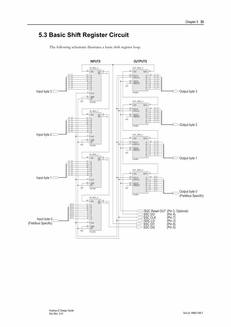
The following schematic illustrates a basic shift register loop.
RCLR
RCLR
RCLR
RCLR
SRCLR
SRCLR
SRCLR
PL
Q7
Q7Q7
Q7
Q7
CKE
CKE
I2 D4
BIT5
I1 D0
I3 D0
I3 D2
I1 D6
O2 D7
O1 D7
O3 D2
I2 D7
BIT1
BIT7
O1 D1
BIT3
O3 D5O3 D6
O1 D5
OUTPUTS
BIT6
I3 D7
O1 D3
I2 D2
O3 D3I3 D3
I1 D2
O3 D0
INPUTS
BIT6
O2 D5I2 D1
BIT3
O3 D4
I2 D3
O1 D2
BIT7
I1 D1
I3 D4
BIT4
BIT1
O2 D0
O1 D4
I2 D5
BIT0
I3 D6
BIT5BIT4
O2 D4
O2 D6
I1 D3
I2 D6
I1 D4
O2 D1O2 D2
I1 D5
BIT0
I3 D5
I3 D1
O2 D3
I1 D7
O1 D6
BIT2
O3 D7
I2 DO
O3 D1
BIT2
O1 D0
OUT_REG_3
74x594
9
1310
14
1112 15
1234567
SDOSDI
SRCLKRCLK A
BCDEFGH
OUT_REG_0
74x594
9
1310
+5V
14
1112 15
1234567
SDO
SRCLR
SDI
SRCLKRCLK A
BCDEFGH
OUT_REG_2
74x594
9
1310
14
1112 15
1234567
SDOSDI
SRCLKRCLK A
BCDEFGH
IN_REG_1
74x165
7910
2
151
111213143456
Q7SDI
CLK
PL
ABCDEFGH
IN_REG_0
74x165
7910
2
151
111213143456
Q7SDI
CLK
CKEPL
ABCDEFGH
IN_REG_2
74x165
7910
2
151
111213143456
SDI
CLK
PL
ABCDEFGH
OUT_REG_1
74x594
9
1310
14
1112 15
1234567
SDOSDI
SRCLKRCLK A
BCDEFGH
IN_REG_3
74x165
7910
2
151
111213143456
Q7SDI
CLK
CKE
ABCDEFGH
/SSC Reset OUT
Input byte 3
SSC DOInput byte 0
(Fieldbus Specific)SSC CLK
Output byte 2
Output byte 3
Output byte 0(Fieldbus Specific)
/SSC LDSSC DI1
Input byte 1
SSC DI2
(Pin 2, Optional)(Pin 4)(Pin 7)(Pin 3)(Pin 6)(Pin 5)
Input byte 2
Output byte 1+5V
+5V
+5V
Chapter 5 34
Doc.Id. HMSI-168-7Anybus-IC Design GuideDoc.Rev. 2.01
5.4 Fieldbus Specific Output Register (Output Register 0)
5.4.1 General
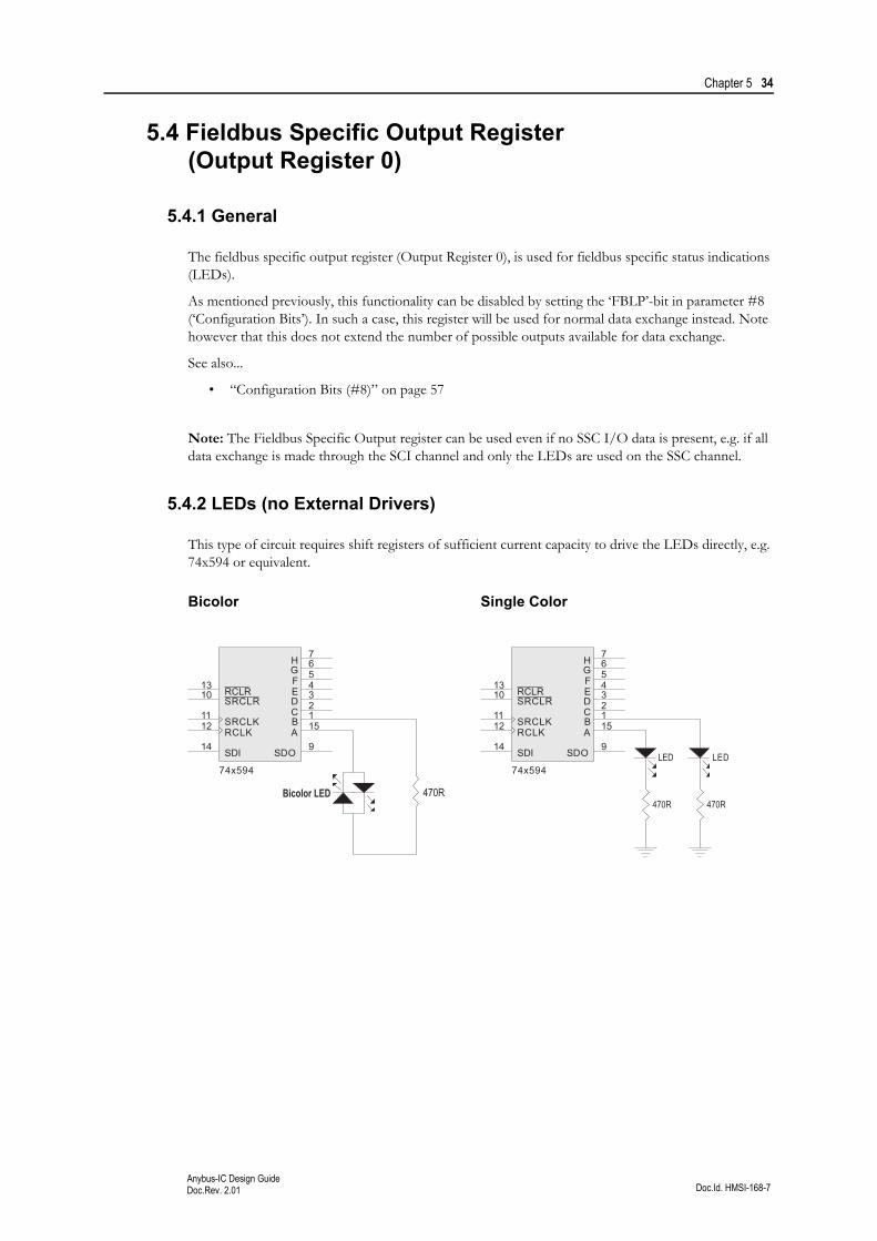
The fieldbus specific output register (Output Register 0), is used for fieldbus specific status indications (LEDs).
As mentioned previously, this functionality can be disabled by setting the ‘FBLP’-bit in parameter #8 (‘Configuration Bits’). In such a case, this register will be used for normal data exchange instead. Note however that this does not extend the number of possible outputs available for data exchange.
See also...
• “Configuration Bits (#8)” on page 57
Note: The Fieldbus Specific Output register can be used even if no SSC I/O data is present, e.g. if all data exchange is made through the SCI channel and only the LEDs are used on the SSC channel.
5.4.2 LEDs (no External Drivers)
This type of circuit requires shift registers of sufficient current capacity to drive the LEDs directly, e.g. 74x594 or equivalent.
SRCLR RCLR
74x594
9
10 13
14
11 12 15
1 2 3 4 5 6 7
SD O SDI
SRCLK RCLK A
B C D E F G H
470R Bicolor LED
SRCLR RCLR
74x594
9
10 13
14
11 12 15
1 2 3 4 5 6 7
SD O SDI
SRCLK RCLK A
B C D E F G H
LED
470R
LED
470R
Bicolor Single Color
Chapter 5 35
Doc.Id. HMSI-168-7Anybus-IC Design GuideDoc.Rev. 2.01
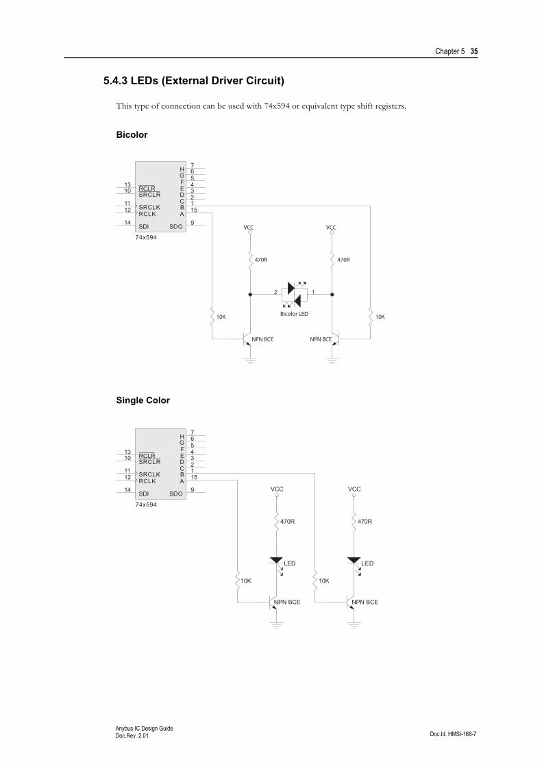
5.4.3 LEDs (External Driver Circuit)
This type of connection can be used with 74x594 or equivalent type shift registers.
Bicolor
Single Color
SRCLR RCLR
74x594
9
10 13
14
11 12 15
1 2 3 4 5 6 7
SD O SDI
SRCLK RCLK A
B C D E F G H
VCC VCC
12
10K10K
470R470R
NPN BCE NPN BCE
Bicolor LED
SRCLR RCLR
74x594
9
10 13
14
11 12 15
1 2 3 4 5 6 7
SD O SDI
SRCLK RCLK A
B C D E F G H
VCC VCC
LED LED
NPN BCE NPN BCE
470R 470R
10K 10K
Chapter 5 36
Doc.Id. HMSI-168-7Anybus-IC Design GuideDoc.Rev. 2.01
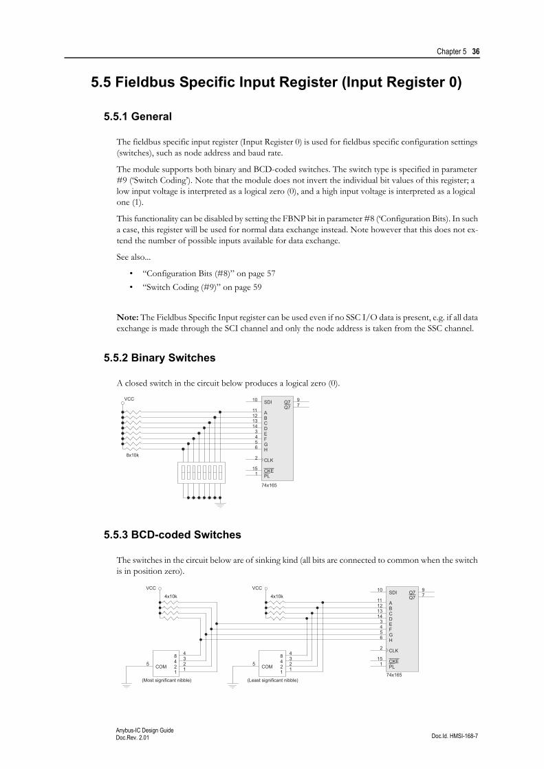
5.5 Fieldbus Specific Input Register (Input Register 0)
5.5.1 General
The fieldbus specific input register (Input Register 0) is used for fieldbus specific configuration settings (switches), such as node address and baud rate.
The module supports both binary and BCD-coded switches. The switch type is specified in parameter #9 (‘Switch Coding’). Note that the module does not invert the individual bit values of this register; a low input voltage is interpreted as a logical zero (0), and a high input voltage is interpreted as a logical one (1).
This functionality can be disabled by setting the FBNP bit in parameter #8 (‘Configuration Bits). In such a case, this register will be used for normal data exchange instead. Note however that this does not ex-tend the number of possible inputs available for data exchange.
See also...
• “Configuration Bits (#8)” on page 57
• “Switch Coding (#9)” on page 59
Note: The Fieldbus Specific Input register can be used even if no SSC I/O data is present, e.g. if all data exchange is made through the SCI channel and only the node address is taken from the SSC channel.
5.5.2 Binary Switches
A closed switch in the circuit below produces a logical zero (0).
5.5.3 BCD-coded Switches
The switches in the circuit below are of sinking kind (all bits are connected to common when the switch is in position zero).
Q7 Q7
PL
VCC
74x165
7 9 10
2
15 1
11 12 13 14
3 4 5 6
SDI
CLK
CKE
A B C D E F G H
8x10k
Q7 Q7
VCC
74x165
7 9 10
2
15 1
11 12 13 14
3 4 5 6
SDI
CLK
CKE PL
A B C D E F G H
4x10k
(Most significant nibble)
1 2 3 4
5
1 2 4 8
COM
(Least significant nibble)
1 2 3 4
5
1 2 4 8
COM
VCC
4x10k
Chapter 5 37
Doc.Id. HMSI-168-7Anybus-IC Design GuideDoc.Rev. 2.01
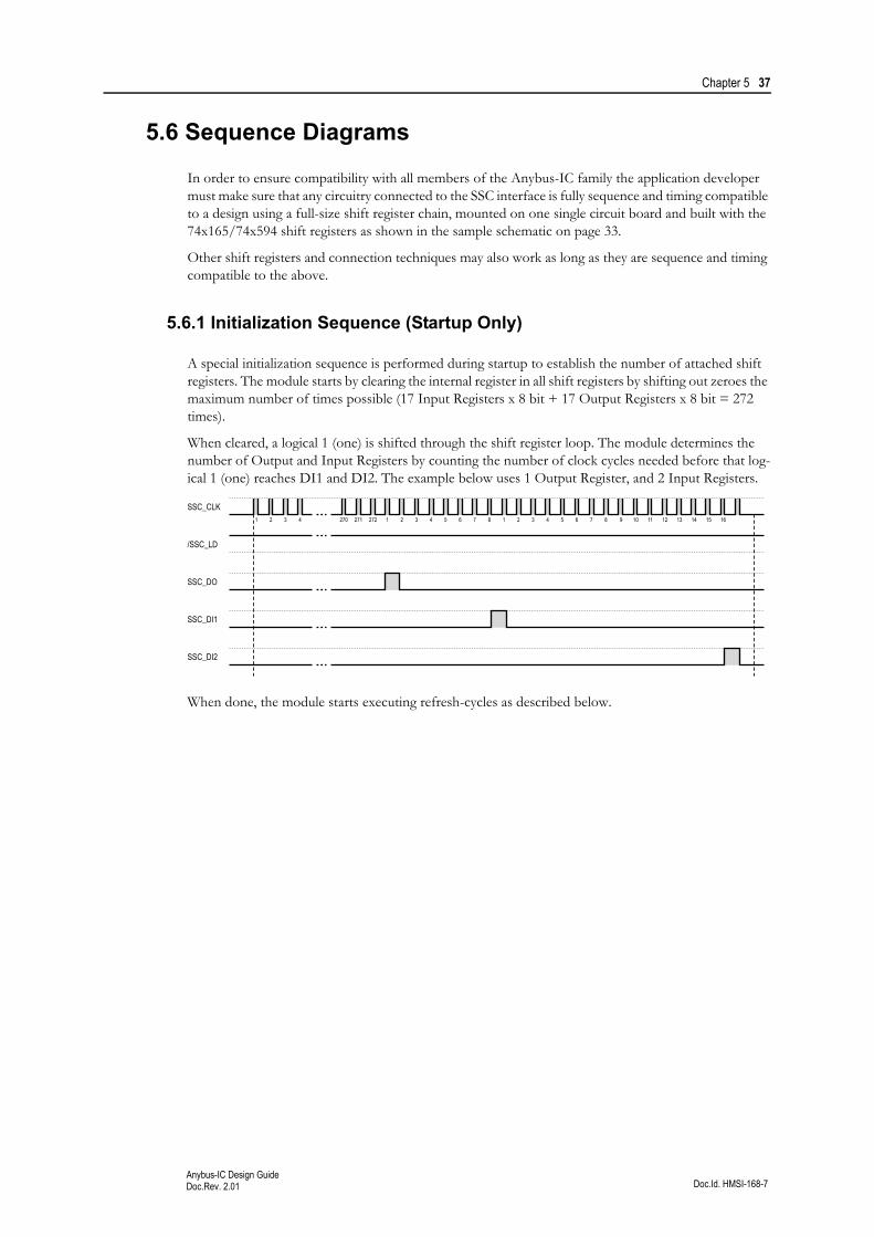
5.6 Sequence Diagrams
In order to ensure compatibility with all members of the Anybus-IC family the application developer must make sure that any circuitry connected to the SSC interface is fully sequence and timing compatible to a design using a full-size shift register chain, mounted on one single circuit board and built with the 74x165/74x594 shift registers as shown in the sample schematic on page 33.
Other shift registers and connection techniques may also work as long as they are sequence and timing compatible to the above.
5.6.1 Initialization Sequence (Startup Only)
A special initialization sequence is performed during startup to establish the number of attached shift registers. The module starts by clearing the internal register in all shift registers by shifting out zeroes the maximum number of times possible (17 Input Registers x 8 bit + 17 Output Registers x 8 bit = 272 times).
When cleared, a logical 1 (one) is shifted through the shift register loop. The module determines the number of Output and Input Registers by counting the number of clock cycles needed before that log-ical 1 (one) reaches DI1 and DI2. The example below uses 1 Output Register, and 2 Input Registers.
When done, the module starts executing refresh-cycles as described below.
SSC_CLK1 2 3 4 270 271 272 1 2 3 4 5 6 7 8 1 2 3 4 5 6 7 8 9 10 11 12 13 14 15 16
/SSC_LD
SSC_DO
SSC_DI1
SSC_DI2
Chapter 5 38
Doc.Id. HMSI-168-7Anybus-IC Design GuideDoc.Rev. 2.01
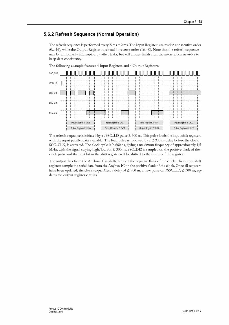
5.6.2 Refresh Sequence (Normal Operation)
The refresh sequence is performed every 5 ms ± 2 ms. The Input Registers are read in consecutive order (0... 16), while the Output Registers are read in reverse order (16... 0). Note that the refresh sequence may be temporarily interrupted by other tasks, but will always finish after the interruption in order to keep data consistency.
The following example features 4 Input Registers and 4 Output Registers.
The refresh sequence is initiated by a /SSC_LD pulse ≥ 300 ns. This pulse loads the input shift registers with the input parallel data available. The load pulse is followed by a ≥ 900 ns delay before the clock, SCC_CLK, is activated. The clock cycle is ≥ 660 ns, giving a maximum frequency of approximately 1,5 MHz, with the signal staying high/low for ≥ 300 ns. SSC_DI2 is sampled on the positive flank of the clock pulse and the next bit in the shift register will be shifted to the output of the register.
The output data from the Anybus-IC is shifted out on the negative flank of the clock. The output shift registers sample the serial data from the Anybus-IC on the positive flank of the clock. Once all registers have been updated, the clock stops. After a delay of ≥ 900 ns, a new pulse on /SSC_LD, ≥ 300 ns, up-dates the output register circuits.
Input Register 0: 0x03 Input Register 1: 0xC3 Input Register 2: 0x07 Input Register 3: 0x00
Output Register 3: 0x5A Output Register 2: 0x01 Output Register 1: 0x00 Output Register 0: 0xFF
SSC_CLK
/SSC_LD
SSC_DO
SSC_DI1
SSC_DI2
Doc.Id. HMSI-168-7Anybus-IC Design GuideDoc.Rev. 2.01
Chapter 6
6. I/O Mapping
6.1 General Information
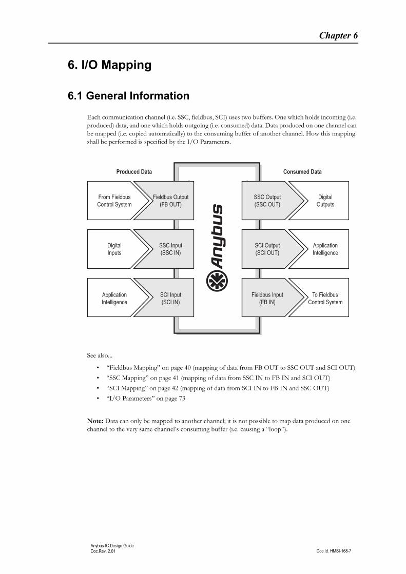
Each communication channel (i.e. SSC, fieldbus, SCI) uses two buffers. One which holds incoming (i.e. produced) data, and one which holds outgoing (i.e. consumed) data. Data produced on one channel can be mapped (i.e. copied automatically) to the consuming buffer of another channel. How this mapping shall be performed is specified by the I/O Parameters.
See also...
• “Fieldbus Mapping” on page 40 (mapping of data from FB OUT to SSC OUT and SCI OUT)
• “SSC Mapping” on page 41 (mapping of data from SSC IN to FB IN and SCI OUT)
• “SCI Mapping” on page 42 (mapping of data from SCI IN to FB IN and SSC OUT)
• “I/O Parameters” on page 73
Note: Data can only be mapped to another channel; it is not possible to map data produced on one channel to the very same channel’s consuming buffer (i.e. causing a “loop”).
Fieldbus Output(FB OUT)
SSC Input(SSC IN)
SCI Input(SCI IN)
From FieldbusControl System
DigitalInputs
ApplicationIntelligence
ApplicationIntelligence
To FieldbusControl System
DigitalOutputs
SSC Output(SSC OUT)
SCI Output(SCI OUT)
Fieldbus Input(FB IN)
Produced Data Consumed Data
Chapter 6 40
Doc.Id. HMSI-168-7Anybus-IC Design GuideDoc.Rev. 2.01
6.2 Fieldbus Mapping
Data written by the fieldbus control system resides in the FB OUT buffer. This data may be mapped, i.e. copied automatically, to SCC OUT and/or SCI OUT.
Related Parameters
Parameter Description
FB Out Actual (#42) Specifies the total size of the FB OUT buffer after initialization. The value specified here is the maximum amount of data that can be mapped to other channels.
SSC Out FB Offset (#57) Specifies the source offset (in the FB OUT buffer) for FB OUT to SCC OUT mapping.
SSC Out FB Size (#58) Specifies the number of bytes to copy from FB OUT to SSC OUT.
SCI Out FB Offset (#67) Specifies the source offset (in the FB OUT buffer) for FB OUT to SCI OUT mapping.
SCI Out FB Size (#68) Specifies the number of bytes to copy from FB OUT to SCI OUT.
FB OUT SSC OUT
SCI OUT
SSC out FB offset (#57)SSC out FB size (#58)
SCI out FB offset (#67)SCI out FB size (#68)FB
out A
ctual
(#42
)
SSC
out A
ctual
(#56
)SC
I out
Actua
l (#66
)
Produced Data Consumed Data
Chapter 6 41
Doc.Id. HMSI-168-7Anybus-IC Design GuideDoc.Rev. 2.01
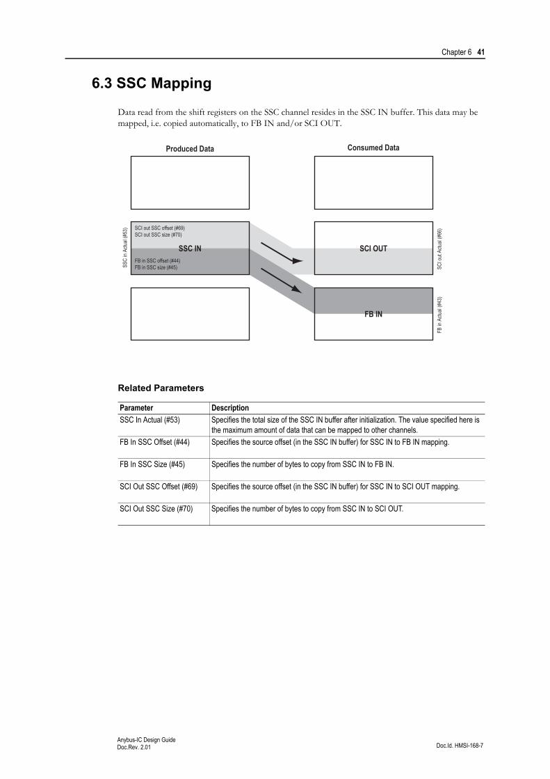
6.3 SSC Mapping
Data read from the shift registers on the SSC channel resides in the SSC IN buffer. This data may be mapped, i.e. copied automatically, to FB IN and/or SCI OUT.
Related Parameters
Parameter Description
SSC In Actual (#53) Specifies the total size of the SSC IN buffer after initialization. The value specified here is the maximum amount of data that can be mapped to other channels.
FB In SSC Offset (#44) Specifies the source offset (in the SSC IN buffer) for SSC IN to FB IN mapping.
FB In SSC Size (#45) Specifies the number of bytes to copy from SSC IN to FB IN.
SCI Out SSC Offset (#69) Specifies the source offset (in the SSC IN buffer) for SSC IN to SCI OUT mapping.
SCI Out SSC Size (#70) Specifies the number of bytes to copy from SSC IN to SCI OUT.
FB IN
FB in
Actu
al (#
43)
SSC IN
SCI out SSC offset (#69)SCI out SSC size (#70)
FB in SSC offset (#44)FB in SSC size (#45)SS
C in
Actua
l (#53
)
SCI OUT
SCI o
ut Ac
tual (#
66)
Produced Data Consumed Data
Chapter 6 42
Doc.Id. HMSI-168-7Anybus-IC Design GuideDoc.Rev. 2.01
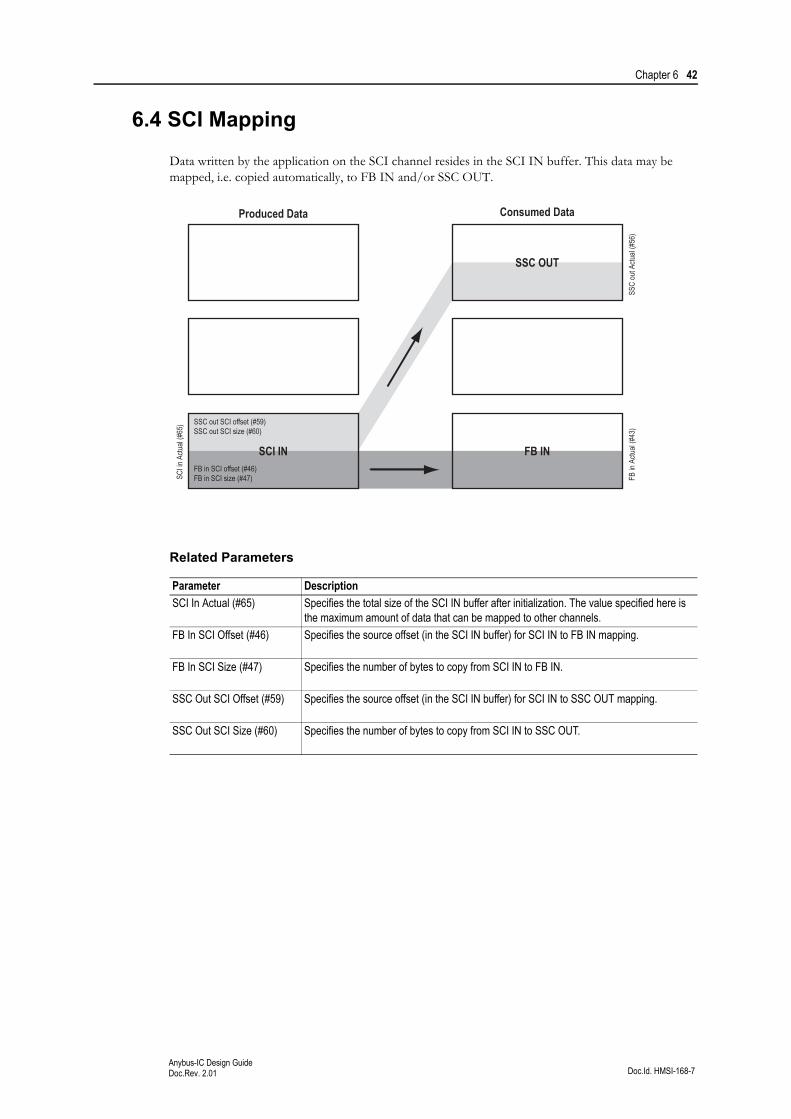
6.4 SCI Mapping
Data written by the application on the SCI channel resides in the SCI IN buffer. This data may be mapped, i.e. copied automatically, to FB IN and/or SSC OUT.
Related Parameters
Parameter Description
SCI In Actual (#65) Specifies the total size of the SCI IN buffer after initialization. The value specified here is the maximum amount of data that can be mapped to other channels.
FB In SCI Offset (#46) Specifies the source offset (in the SCI IN buffer) for SCI IN to FB IN mapping.
FB In SCI Size (#47) Specifies the number of bytes to copy from SCI IN to FB IN.
SSC Out SCI Offset (#59) Specifies the source offset (in the SCI IN buffer) for SCI IN to SSC OUT mapping.
SSC Out SCI Size (#60) Specifies the number of bytes to copy from SCI IN to SSC OUT.
SSC OUT
FB IN
FB in
Actu
al (#
43)
SCI IN
SSC out SCI offset (#59)SSC out SCI size (#60)
FB in SCI offset (#46)FB in SCI size (#47)SC
I in A
ctual
(#65
)
SSC
out A
ctual
(#56
)
Produced Data Consumed Data
Doc.Id. HMSI-168-7Anybus-IC Design GuideDoc.Rev. 2.01
Chapter 7
7. Initialization
7.1 General Information
The Anybus module features three modes of operation:
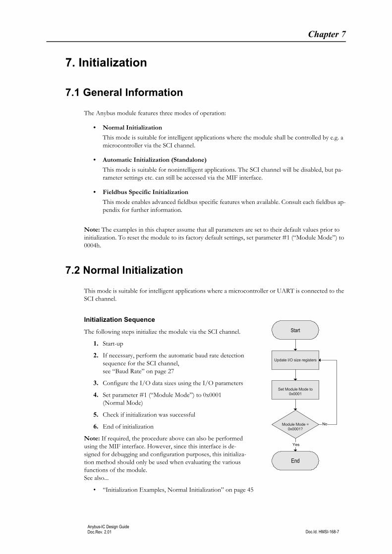
• Normal Initialization
This mode is suitable for intelligent applications where the module shall be controlled by e.g. a microcontroller via the SCI channel.
• Automatic Initialization (Standalone)
This mode is suitable for nonintelligent applications. The SCI channel will be disabled, but pa-rameter settings etc. can still be accessed via the MIF interface.
• Fieldbus Specific Initialization
This mode enables advanced fieldbus specific features when available. Consult each fieldbus ap-pendix for further information.
Note: The examples in this chapter assume that all parameters are set to their default values prior to initialization. To reset the module to its factory default settings, set parameter #1 (“Module Mode”) to 0004h.
7.2 Normal Initialization
This mode is suitable for intelligent applications where a microcontroller or UART is connected to the SCI channel.
Initialization Sequence
The following steps initialize the module via the SCI channel.
1. Start-up
2. If necessary, perform the automatic baud rate detection sequence for the SCI channel, see “Baud Rate” on page 27
3. Configure the I/O data sizes using the I/O parameters
4. Set parameter #1 (“Module Mode”) to 0x0001(Normal Mode)
5. Check if initialization was successful
6. End of initialization
Note: If required, the procedure above can also be performed using the MIF interface. However, since this interface is de-signed for debugging and configuration purposes, this initializa-tion method should only be used when evaluating the various functions of the module.See also...
• “Initialization Examples, Normal Initialization” on page 45
Yes
Start
End
Update I/O size registers
Set Module Mode to0x0001
Module Mode =0x0001?
No
Chapter 7 44
Doc.Id. HMSI-168-7Anybus-IC Design GuideDoc.Rev. 2.01
7.3 Automatic Initialization (Standalone)
Connecting SCI_DE [AUTO] (pin 29) to ground (GND) will cause the module to initialize itself auto-matically to run “standalone”. This mode is intended for nonintelligent applications such as valve termi-nals and modular I/O devices.
Automatic initialization affects the implementation as follows:
• The SCI channel will be completely disabled, and SCI related parameters will either be set to zero or ignored, depending on context. Parameters can however still be set via the MIF interface.
• SSC- and fieldbus related I/O parameters will be set automatically based on the shift register con-figuration. All SSC data will be mapped to the fieldbus and vice versa.
• The settings in parameter #8 (‘Configuration Bits’) will be set to reflect standalone operation.
Note: If parameter #8 “Configuration Bits” is set to a value different than zero (0000h), the au-tomatic initialization may not work as expected (e.g. if the SSCI bit is 1, the SSC Input data size will be taken from parameter #51 “SSC In Config” instead of the automatically detected size). To reset the module to its factory default settings, set parameter #1 (“Module Mode”) to 0004h.
See also...
• “Application Connector” on page 14 (pin 29)
• “MIF Interface” on page 21
• “SSC Channel” on page 31
• “Initialization Examples, Automatic Initialization” on page 49
• “General Parameters” on page 52 ( “Configuration Bits (#8)” on page 57)
• “I/O Parameters” on page 73
7.4 Fieldbus Specific Initialization
For advanced implementations, certain Anybus-IC versions feature special initialization modes which provide support for advanced fieldbus specific functions.
For more information, consult each separate fieldbus appendix.
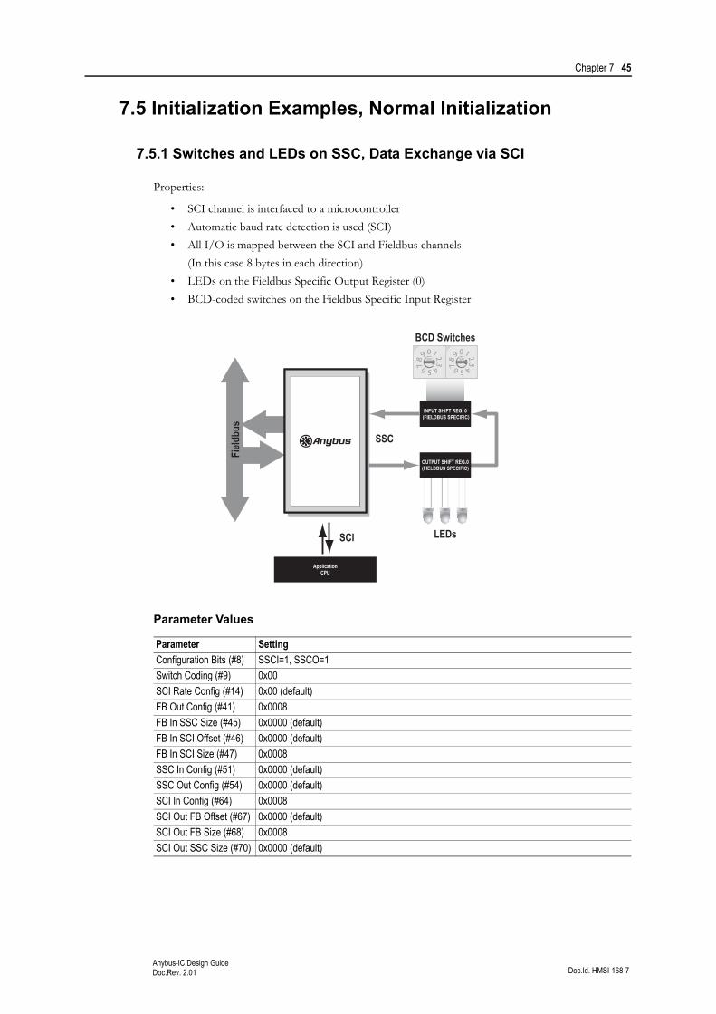
Chapter 7 45
Doc.Id. HMSI-168-7Anybus-IC Design GuideDoc.Rev. 2.01
7.5 Initialization Examples, Normal Initialization
7.5.1 Switches and LEDs on SSC, Data Exchange via SCI
Properties:
• SCI channel is interfaced to a microcontroller
• Automatic baud rate detection is used (SCI)
• All I/O is mapped between the SCI and Fieldbus channels
(In this case 8 bytes in each direction)
• LEDs on the Fieldbus Specific Output Register (0)
• BCD-coded switches on the Fieldbus Specific Input Register
Parameter Values
Parameter Setting
Configuration Bits (#8) SSCI=1, SSCO=1
Switch Coding (#9) 0x00
SCI Rate Config (#14) 0x00 (default)
FB Out Config (#41) 0x0008
FB In SSC Size (#45) 0x0000 (default)
FB In SCI Offset (#46) 0x0000 (default)
FB In SCI Size (#47) 0x0008
SSC In Config (#51) 0x0000 (default)
SSC Out Config (#54) 0x0000 (default)
SCI In Config (#64) 0x0008
SCI Out FB Offset (#67) 0x0000 (default)
SCI Out FB Size (#68) 0x0008
SCI Out SSC Size (#70) 0x0000 (default)
INPUT SHIFT REG. 0 (FIELDBUS SPECIFIC)
BCD Switches
LEDs
OUTPUT SHIFT REG.0(FIELDBUS SPECIFIC)
SSC
Field
bus
ApplicationCPU
SCI
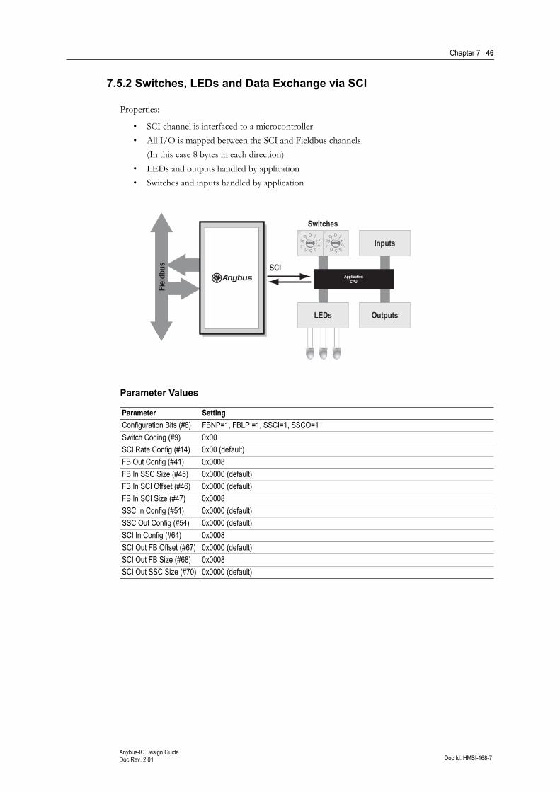
Chapter 7 46
Doc.Id. HMSI-168-7Anybus-IC Design GuideDoc.Rev. 2.01
7.5.2 Switches, LEDs and Data Exchange via SCI
Properties:
• SCI channel is interfaced to a microcontroller
• All I/O is mapped between the SCI and Fieldbus channels
(In this case 8 bytes in each direction)
• LEDs and outputs handled by application
• Switches and inputs handled by application
Parameter Values
Parameter Setting
Configuration Bits (#8) FBNP=1, FBLP =1, SSCI=1, SSCO=1
Switch Coding (#9) 0x00
SCI Rate Config (#14) 0x00 (default)
FB Out Config (#41) 0x0008
FB In SSC Size (#45) 0x0000 (default)
FB In SCI Offset (#46) 0x0000 (default)
FB In SCI Size (#47) 0x0008
SSC In Config (#51) 0x0000 (default)
SSC Out Config (#54) 0x0000 (default)
SCI In Config (#64) 0x0008
SCI Out FB Offset (#67) 0x0000 (default)
SCI Out FB Size (#68) 0x0008
SCI Out SSC Size (#70) 0x0000 (default)
Field
bus
LEDs
Switches
Outputs
Inputs
ApplicationCPU
SCI
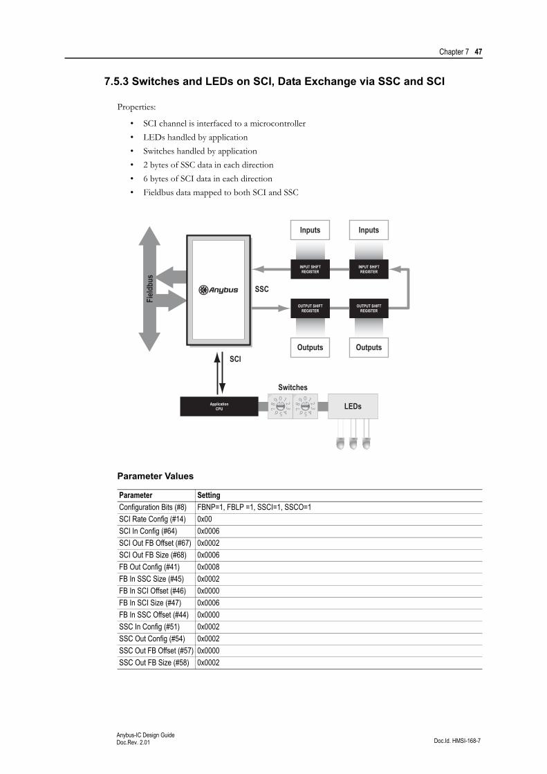
Chapter 7 47
Doc.Id. HMSI-168-7Anybus-IC Design GuideDoc.Rev. 2.01
7.5.3 Switches and LEDs on SCI, Data Exchange via SSC and SCI
Properties:
• SCI channel is interfaced to a microcontroller
• LEDs handled by application
• Switches handled by application
• 2 bytes of SSC data in each direction
• 6 bytes of SCI data in each direction
• Fieldbus data mapped to both SCI and SSC
Parameter Values
Parameter Setting
Configuration Bits (#8) FBNP=1, FBLP =1, SSCI=1, SSCO=1
SCI Rate Config (#14) 0x00
SCI In Config (#64) 0x0006
SCI Out FB Offset (#67) 0x0002
SCI Out FB Size (#68) 0x0006
FB Out Config (#41) 0x0008
FB In SSC Size (#45) 0x0002
FB In SCI Offset (#46) 0x0000
FB In SCI Size (#47) 0x0006
FB In SSC Offset (#44) 0x0000
SSC In Config (#51) 0x0002
SSC Out Config (#54) 0x0002
SSC Out FB Offset (#57) 0x0000
SSC Out FB Size (#58) 0x0002
Field
bus
LEDs
Switches
ApplicationCPU
SCI
INPUT SHIFTREGISTER
Inputs
Outputs
OUTPUT SHIFTREGISTER
INPUT SHIFTREGISTER
OUTPUT SHIFTREGISTER
SSC
Inputs
Outputs
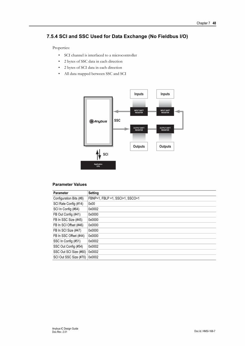
Chapter 7 48
Doc.Id. HMSI-168-7Anybus-IC Design GuideDoc.Rev. 2.01
7.5.4 SCI and SSC Used for Data Exchange (No Fieldbus I/O)
Properties:
• SCI channel is interfaced to a microcontroller
• 2 bytes of SSC data in each direction
• 2 bytes of SCI data in each direction
• All data mapped between SSC and SCI
Parameter Values
Parameter Setting
Configuration Bits (#8) FBNP=1, FBLP =1, SSCI=1, SSCO=1
SCI Rate Config (#14) 0x00
SCI In Config (#64) 0x0002
FB Out Config (#41) 0x0000
FB In SSC Size (#45) 0x0000
FB In SCI Offset (#46) 0x0000
FB In SCI Size (#47) 0x0000
FB In SSC Offset (#44) 0x0000
SSC In Config (#51) 0x0002
SSC Out Config (#54) 0x0002
SSC Out SCI Size (#60) 0x0002
SCI Out SSC Size (#70) 0x0002
ApplicationCPU
SCI
INPUT SHIFTREGISTER
Inputs
Outputs
OUTPUT SHIFTREGISTER
INPUT SHIFTREGISTER
OUTPUT SHIFTREGISTER
SSC
Inputs
Outputs
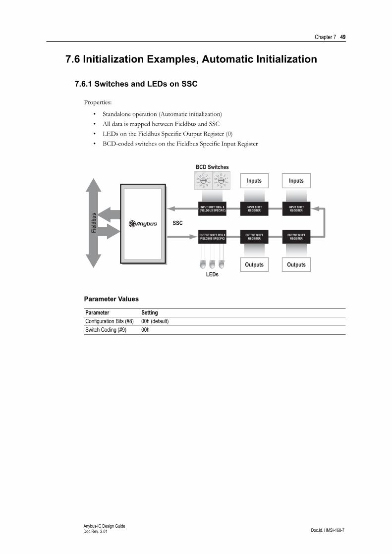
Chapter 7 49
Doc.Id. HMSI-168-7Anybus-IC Design GuideDoc.Rev. 2.01
7.6 Initialization Examples, Automatic Initialization
7.6.1 Switches and LEDs on SSC
Properties:
• Standalone operation (Automatic initialization)
• All data is mapped between Fieldbus and SSC
• LEDs on the Fieldbus Specific Output Register (0)
• BCD-coded switches on the Fieldbus Specific Input Register
Parameter Values
Parameter Setting
Configuration Bits (#8) 00h (default)
Switch Coding (#9) 00h
Field
bus
INPUT SHIFTREGISTER
Inputs
Outputs
OUTPUT SHIFTREGISTER
INPUT SHIFT REG. 0 (FIELDBUS SPECIFIC)
INPUT SHIFTREGISTER
OUTPUT SHIFTREGISTER
BCD Switches
SSC
Inputs
LEDsOutputs
OUTPUT SHIFT REG.0(FIELDBUS SPECIFIC)
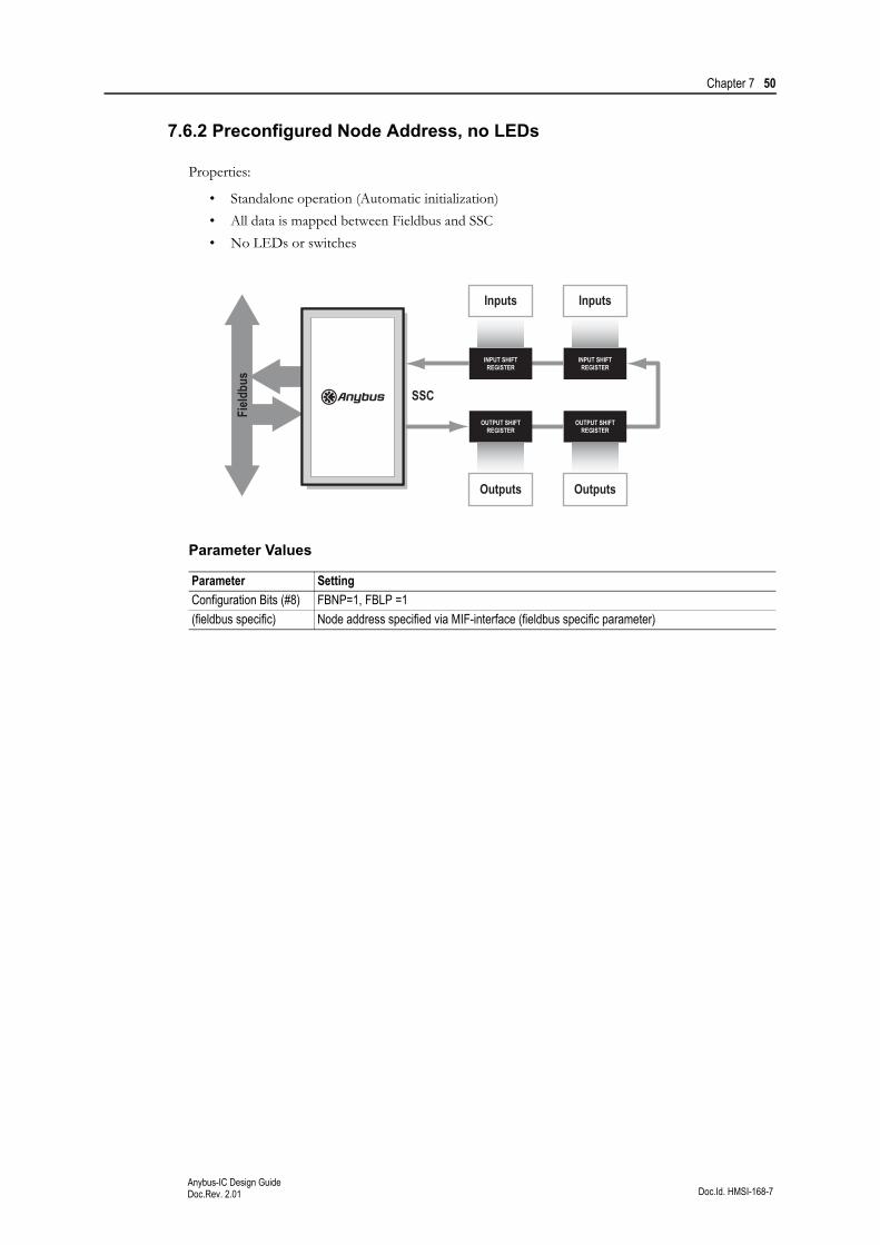
Chapter 7 50
Doc.Id. HMSI-168-7Anybus-IC Design GuideDoc.Rev. 2.01
7.6.2 Preconfigured Node Address, no LEDs
Properties:
• Standalone operation (Automatic initialization)
• All data is mapped between Fieldbus and SSC
• No LEDs or switches
Parameter Values
Parameter Setting
Configuration Bits (#8) FBNP=1, FBLP =1
(fieldbus specific) Node address specified via MIF-interface (fieldbus specific parameter)
Field
bus
INPUT SHIFTREGISTER
Inputs
Outputs
OUTPUT SHIFTREGISTER
INPUT SHIFTREGISTER
OUTPUT SHIFTREGISTER
SSC
Inputs
Outputs
Doc.Id. HMSI-168-7Anybus-IC Design GuideDoc.Rev. 2.01
Chapter 8
8. Parameters
8.1 General Information
From the host application side, all settings and data in the module are represented through entities called ‘Parameters’. Parameters can be accessed by the user through the MIF interface, or by the application via the SCI channel.
The parameters are grouped into three categories based on their usage as follows:
• General Anybus-IC Parameters
Used for configuration and status information, present on all versions of the Anybus-IC.
• I/O Parameters
Specifies data sizes and I/O mapping, present on all versions of the Anybus-IC.
• Fieldbus Specific Parameters
Entirely fieldbus specific; consult each separate fieldbus appendix for further information.
Note 1: When accessing parameters via the SCI channel (e.g. using Modbus), byte-sized parameter val-ues are placed in the least significant byte of the word.
Note 2: In this document, register numbers are specified using the protocol convention (base 0), i.e. there is a 1:1 correlation between the register number specified in this document and the actual register value in the message frame.
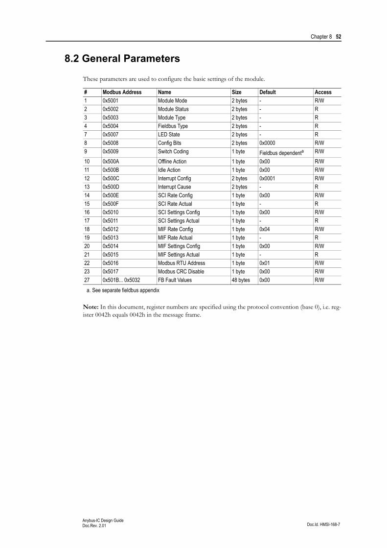
Chapter 8 52
Doc.Id. HMSI-168-7Anybus-IC Design GuideDoc.Rev. 2.01
8.2 General Parameters
These parameters are used to configure the basic settings of the module.
Note: In this document, register numbers are specified using the protocol convention (base 0), i.e. reg-ister 0042h equals 0042h in the message frame.
# Modbus Address Name Size Default Access
1 0x5001 Module Mode 2 bytes - R/W
2 0x5002 Module Status 2 bytes - R
3 0x5003 Module Type 2 bytes - R
4 0x5004 Fieldbus Type 2 bytes - R
7 0x5007 LED State 2 bytes - R
8 0x5008 Config Bits 2 bytes 0x0000 R/W
9 0x5009 Switch Coding 1 byte Fieldbus dependenta
a. See separate fieldbus appendix
R/W
10 0x500A Offline Action 1 byte 0x00 R/W
11 0x500B Idle Action 1 byte 0x00 R/W
12 0x500C Interrupt Config 2 bytes 0x0001 R/W
13 0x500D Interrupt Cause 2 bytes - R
14 0x500E SCI Rate Config 1 byte 0x00 R/W
15 0x500F SCI Rate Actual 1 byte - R
16 0x5010 SCI Settings Config 1 byte 0x00 R/W
17 0x5011 SCI Settings Actual 1 byte - R
18 0x5012 MIF Rate Config 1 byte 0x04 R/W
19 0x5013 MIF Rate Actual 1 byte - R
20 0x5014 MIF Settings Config 1 byte 0x00 R/W
21 0x5015 MIF Settings Actual 1 byte - R
22 0x5016 Modbus RTU Address 1 byte 0x01 R/W
23 0x5017 Modbus CRC Disable 1 byte 0x00 R/W
27 0x501B... 0x5032 FB Fault Values 48 bytes 0x00 R/W
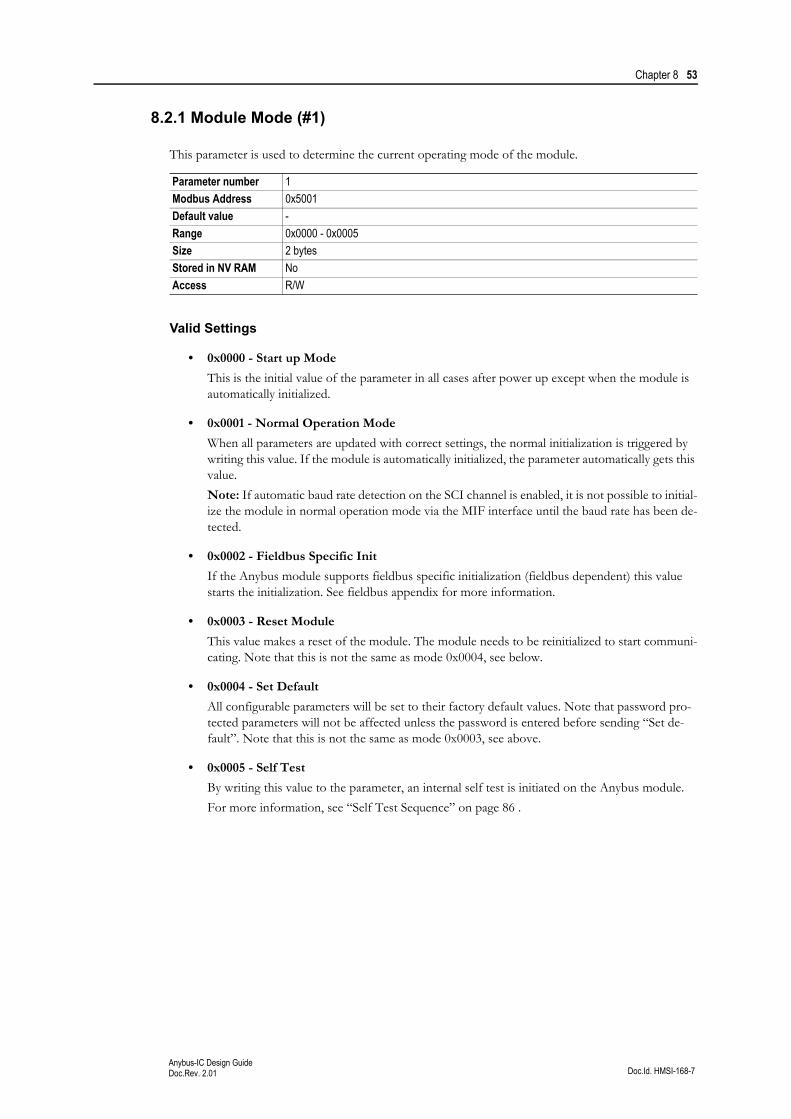
Chapter 8 53
Doc.Id. HMSI-168-7Anybus-IC Design GuideDoc.Rev. 2.01
8.2.1 Module Mode (#1)
This parameter is used to determine the current operating mode of the module.
Valid Settings
• 0x0000 - Start up Mode
This is the initial value of the parameter in all cases after power up except when the module is automatically initialized.
• 0x0001 - Normal Operation Mode
When all parameters are updated with correct settings, the normal initialization is triggered by writing this value. If the module is automatically initialized, the parameter automatically gets this value.
Note: If automatic baud rate detection on the SCI channel is enabled, it is not possible to initial-ize the module in normal operation mode via the MIF interface until the baud rate has been de-tected.
• 0x0002 - Fieldbus Specific Init
If the Anybus module supports fieldbus specific initialization (fieldbus dependent) this value starts the initialization. See fieldbus appendix for more information.
• 0x0003 - Reset Module
This value makes a reset of the module. The module needs to be reinitialized to start communi-cating. Note that this is not the same as mode 0x0004, see below.
• 0x0004 - Set Default
All configurable parameters will be set to their factory default values. Note that password pro-tected parameters will not be affected unless the password is entered before sending “Set de-fault”. Note that this is not the same as mode 0x0003, see above.
• 0x0005 - Self Test
By writing this value to the parameter, an internal self test is initiated on the Anybus module.
For more information, see “Self Test Sequence” on page 86 .
Parameter number 1
Modbus Address 0x5001
Default value -
Range 0x0000 - 0x0005
Size 2 bytes
Stored in NV RAM No
Access R/W
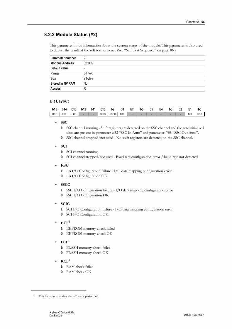
Chapter 8 54
Doc.Id. HMSI-168-7Anybus-IC Design GuideDoc.Rev. 2.01
8.2.2 Module Status (#2)
This parameter holds information about the current status of the module. This parameter is also used to deliver the result of the self test sequence (See “Self Test Sequence” on page 86 )
Bit Layout
• SSC1: SSC channel running - Shift registers are detected on the SSC channel and the autoinitialized
sizes are present in parameter #52 “SSC In Auto” and parameter #55 “SSC Out Auto”.0: SSC channel stopped/not used - No shift registers are detected on the SSC channel.
• SCI1: SCI channel running0: SCI channel stopped/not used - Baud rate configuration error / baud rate not detected
• FBC1: FB I/O Configuration failure - I/O data mapping configuration error0: FB I/O Configuration OK
• SSCC
1: SSC I/O Configuration failure - I/O data mapping configuration error0: SSC I/O Configuration OK
• SCIC1: SCI I/O Configuration failure - I/O data mapping configuration error0: SCI I/O Configuration OK
• ECF1
1: EEPROM memory check failed0: EEPROM memory check OK
• FCF1
1: FLASH memory check failed0: FLASH memory check OK
• RCF1
1: RAM check failed0: RAM check OK
Parameter number 2
Modbus Address 0x5002
Default value -
Range Bit field
Size 2 bytes
Stored in NV RAM No
Access R
b15 b14 b13 b12 b11 b10 b9 b8 b7 b6 b5 b4 b3 b2 b1 b0RCF FCF ECF - - SCIC SSCC FBC - - - - - - SCI SSC
1. This bit is only set after the self test is performed.
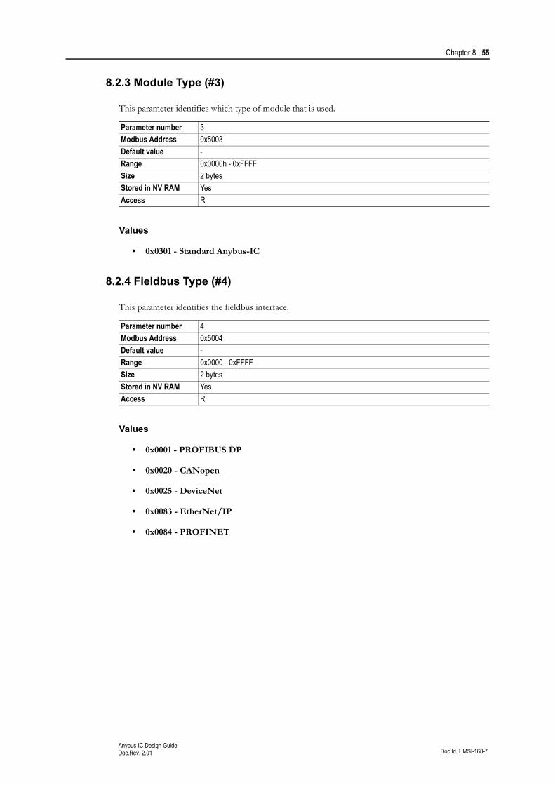
Chapter 8 55
Doc.Id. HMSI-168-7Anybus-IC Design GuideDoc.Rev. 2.01
8.2.3 Module Type (#3)
This parameter identifies which type of module that is used.
Values
• 0x0301 - Standard Anybus-IC
8.2.4 Fieldbus Type (#4)
This parameter identifies the fieldbus interface.
Values
• 0x0001 - PROFIBUS DP
• 0x0020 - CANopen
• 0x0025 - DeviceNet
• 0x0083 - EtherNet/IP
• 0x0084 - PROFINET
Parameter number 3
Modbus Address 0x5003
Default value -
Range 0x0000h - 0xFFFF
Size 2 bytes
Stored in NV RAM Yes
Access R
Parameter number 4
Modbus Address 0x5004
Default value -
Range 0x0000 - 0xFFFF
Size 2 bytes
Stored in NV RAM Yes
Access R
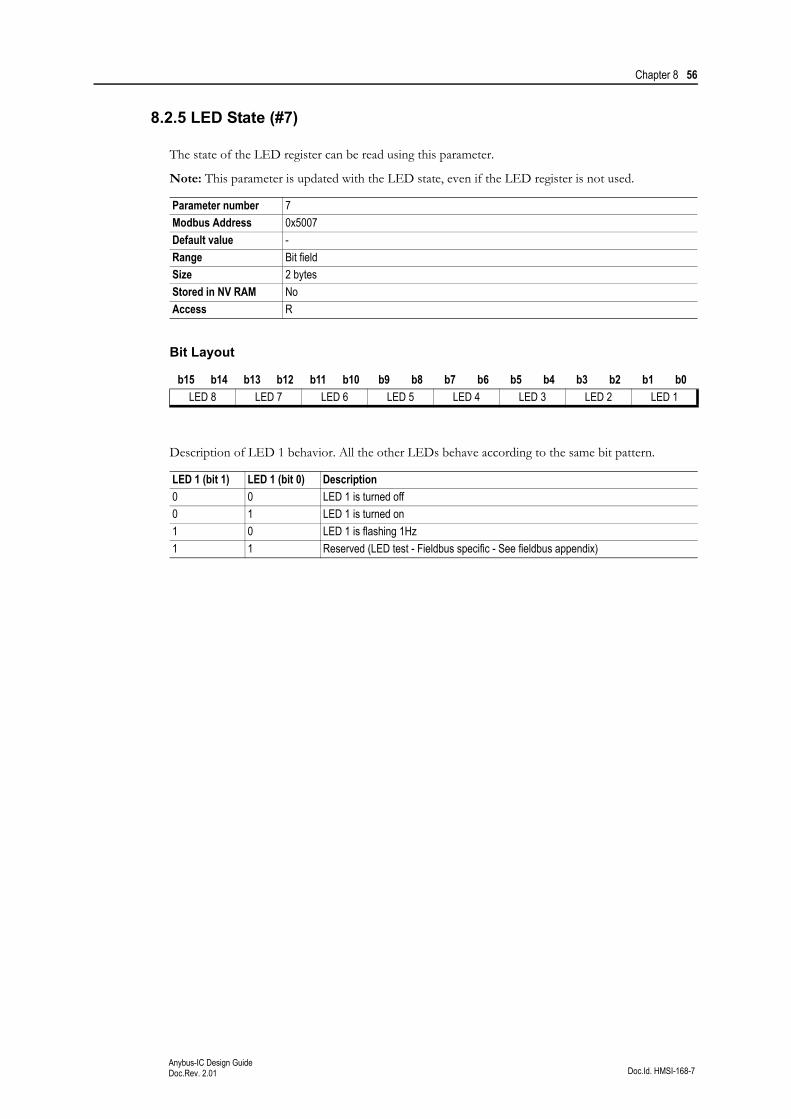
Chapter 8 56
Doc.Id. HMSI-168-7Anybus-IC Design GuideDoc.Rev. 2.01
8.2.5 LED State (#7)
The state of the LED register can be read using this parameter.
Note: This parameter is updated with the LED state, even if the LED register is not used.
Bit Layout
Description of LED 1 behavior. All the other LEDs behave according to the same bit pattern.
Parameter number 7
Modbus Address 0x5007
Default value -
Range Bit field
Size 2 bytes
Stored in NV RAM No
Access R
b15 b14 b13 b12 b11 b10 b9 b8 b7 b6 b5 b4 b3 b2 b1 b0
LED 8 LED 7 LED 6 LED 5 LED 4 LED 3 LED 2 LED 1
LED 1 (bit 1) LED 1 (bit 0) Description
0 0 LED 1 is turned off
0 1 LED 1 is turned on
1 0 LED 1 is flashing 1Hz
1 1 Reserved (LED test - Fieldbus specific - See fieldbus appendix)
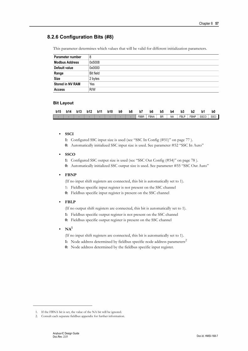
Chapter 8 57
Doc.Id. HMSI-168-7Anybus-IC Design GuideDoc.Rev. 2.01
8.2.6 Configuration Bits (#8)
This parameter determines which values that will be valid for different initialization parameters.
Bit Layout
• SSCI
1: Configured SSC input size is used (see “SSC In Config (#51)” on page 77 ).0: Automatically initialized SSC input size is used. See parameter #52 “SSC In Auto”
• SSCO1: Configured SSC output size is used (see “SSC Out Config (#54)” on page 78 ).0: Automatically initialized SSC output size is used. See parameter #55 “SSC Out Auto”
• FBNP
(If no input shift registers are connected, this bit is automatically set to 1).
1: Fieldbus specific input register is not present on the SSC channel0: Fieldbus specific input register is present on the SSC channel
• FBLP
(If no output shift registers are connected, this bit is automatically set to 1).
1: Fieldbus specific output register is not present on the SSC channel0: Fieldbus specific output register is present on the SSC channel
• NA1
(If no input shift registers are connected, this bit is automatically set to 1).
1: Node address determined by fieldbus specific node address parameters2
0: Node address determined by the fieldbus specific input register.
Parameter number 8
Modbus Address 0x5008
Default value 0x0000
Range Bit field
Size 2 bytes
Stored in NV RAM Yes
Access R/W
b15 b14 b13 b12 b11 b10 b9 b8 b7 b6 b5 b4 b3 b2 b1 b0- - - - - - - - FBBR FBNA BR NA FBLP FBNP SSCO SSCI
1. If the FBNA bit is set, the value of the NA bit will be ignored.2. Consult each separate fieldbus appendix for further information.
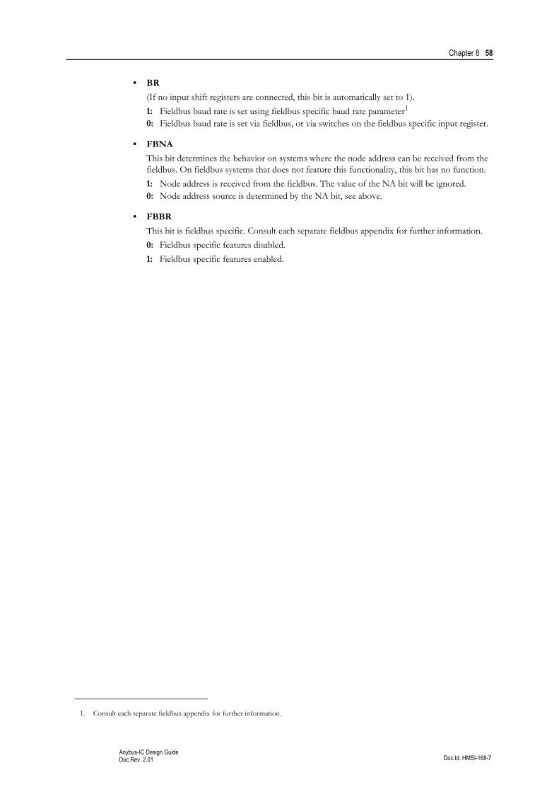
Chapter 8 58
Doc.Id. HMSI-168-7Anybus-IC Design GuideDoc.Rev. 2.01
• BR
(If no input shift registers are connected, this bit is automatically set to 1).
1: Fieldbus baud rate is set using fieldbus specific baud rate parameter1
0: Fieldbus baud rate is set via fieldbus, or via switches on the fieldbus specific input register.
• FBNA
This bit determines the behavior on systems where the node address can be received from the fieldbus. On fieldbus systems that does not feature this functionality, this bit has no function.
1: Node address is received from the fieldbus. The value of the NA bit will be ignored.0: Node address source is determined by the NA bit, see above.
• FBBR
This bit is fieldbus specific. Consult each separate fieldbus appendix for further information.
0: Fieldbus specific features disabled.
1: Fieldbus specific features enabled.
1. Consult each separate fieldbus appendix for further information.
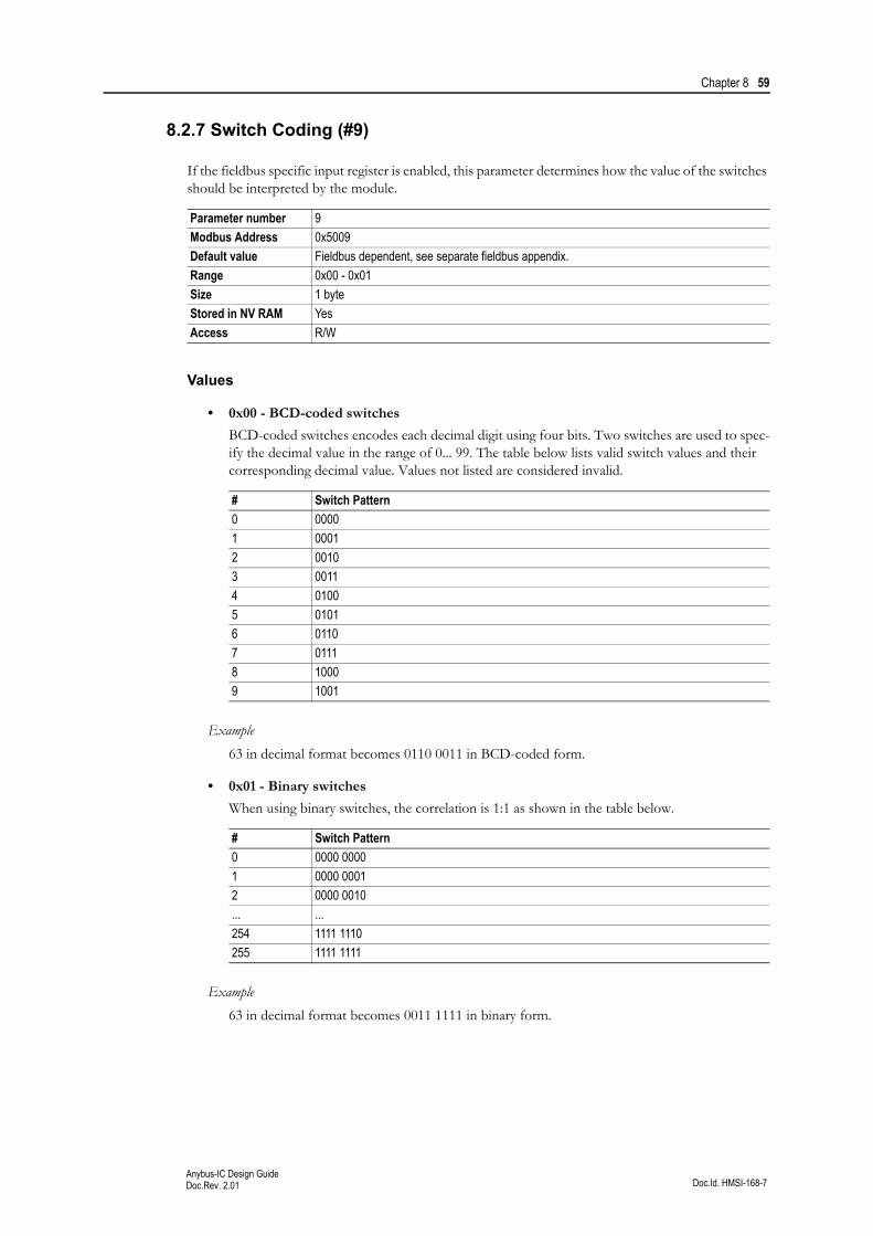
Chapter 8 59
Doc.Id. HMSI-168-7Anybus-IC Design GuideDoc.Rev. 2.01
8.2.7 Switch Coding (#9)
If the fieldbus specific input register is enabled, this parameter determines how the value of the switches should be interpreted by the module.
Values
• 0x00 - BCD-coded switches
BCD-coded switches encodes each decimal digit using four bits. Two switches are used to spec-ify the decimal value in the range of 0... 99. The table below lists valid switch values and their corresponding decimal value. Values not listed are considered invalid.
Example
63 in decimal format becomes 0110 0011 in BCD-coded form.
• 0x01 - Binary switches
When using binary switches, the correlation is 1:1 as shown in the table below.
Example
63 in decimal format becomes 0011 1111 in binary form.
Parameter number 9
Modbus Address 0x5009
Default value Fieldbus dependent, see separate fieldbus appendix.
Range 0x00 - 0x01
Size 1 byte
Stored in NV RAM Yes
Access R/W
# Switch Pattern
0 0000
1 0001
2 0010
3 0011
4 0100
5 0101
6 0110
7 0111
8 1000
9 1001
# Switch Pattern
0 0000 0000
1 0000 0001
2 0000 0010
... ...
254 1111 1110
255 1111 1111

Chapter 8 60
Doc.Id. HMSI-168-7Anybus-IC Design GuideDoc.Rev. 2.01
8.2.8 Offline Action Config (#10)
When the fieldbus goes from online to offline or from idle to offline, the fieldbus outputs can be con-figured to behave in different ways.
Note: The module must have been online once for the offline action to take effect.
Values
• 0x00 - Clear
Fieldbus outputs are cleared when the fieldbus goes offline.
• 0x01 - Freeze
Fieldbus outputs freeze in the states they are in when the fieldbus goes offline.
• 0x02 - Fault values
Fault values configured in parameter #27 “FB Fault Values” are copied to the fieldbus outputs when the fieldbus goes offline.
Parameter number 10
Modbus Address 0x500A
Default value 0x00
Range 0x00 - 0x02
Size 1 byte
Stored in NV RAM Yes
Access R/W
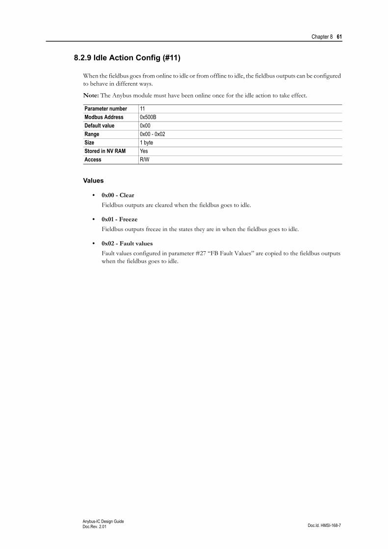
Chapter 8 61
Doc.Id. HMSI-168-7Anybus-IC Design GuideDoc.Rev. 2.01
8.2.9 Idle Action Config (#11)
When the fieldbus goes from online to idle or from offline to idle, the fieldbus outputs can be configured to behave in different ways.
Note: The Anybus module must have been online once for the idle action to take effect.
Values
• 0x00 - Clear
Fieldbus outputs are cleared when the fieldbus goes to idle.
• 0x01 - Freeze
Fieldbus outputs freeze in the states they are in when the fieldbus goes to idle.
• 0x02 - Fault values
Fault values configured in parameter #27 “FB Fault Values” are copied to the fieldbus outputs when the fieldbus goes to idle.
Parameter number 11
Modbus Address 0x500B
Default value 0x00
Range 0x00 - 0x02
Size 1 byte
Stored in NV RAM Yes
Access R/W

Chapter 8 62
Doc.Id. HMSI-168-7Anybus-IC Design GuideDoc.Rev. 2.01
8.2.10 Interrupt Config (#12)
This parameter defines events that are allowed to trigger an interrupt. See also parameter #13 “Interrupt Cause”.
Bit Layout
• START1
1: An interrupt will be generated when the module has started from power on and is ready to communicate.
0: This event will not cause an interrupt.
• FBON1: An interrupt will be generated when the fieldbus goes from offline to online.0: This event will not cause an interrupt.
• FBOFF
1: An interrupt will be generated when the fieldbus goes from online to offline.
0: This event will not cause an interrupt.
• ACYC2
1: An interrupt will be generated when new acyclic data is received from the fieldbus master. 0: This event will not cause an interrupt.
• DEF2
1: An interrupt will be generated when “set default” is received from the fieldbus master.0: This event will not cause an interrupt.
• RES2
1: An interrupt will be generated when “reset” is received from the fieldbus master.
0: This event will not cause an interrupt.
• IDLE2
1: An interrupt will be generated when the fieldbus goes from online to idle or from offline to idle.
0: This event will not cause an interrupt.
Parameter number 12
Modbus Address 0x500C
Default value 0x0001
Range Bit field
Size 2 bytes
Stored in NV RAM Yes
Access R/W
b15 b14 b13 b12 b11 b10 b9 b8 b7 b6 b5 b4 b3 b2 b1 b0- - - - - - - - - IDLE RES DEF ACYC FBOFF FBON START
1. If automatic baud rate detection is used, the interrupt is not generated until the correct baud rate is detected.2. This bit is fieldbus dependent, i.e. it may not be available on all versions of the Anybus-IC.
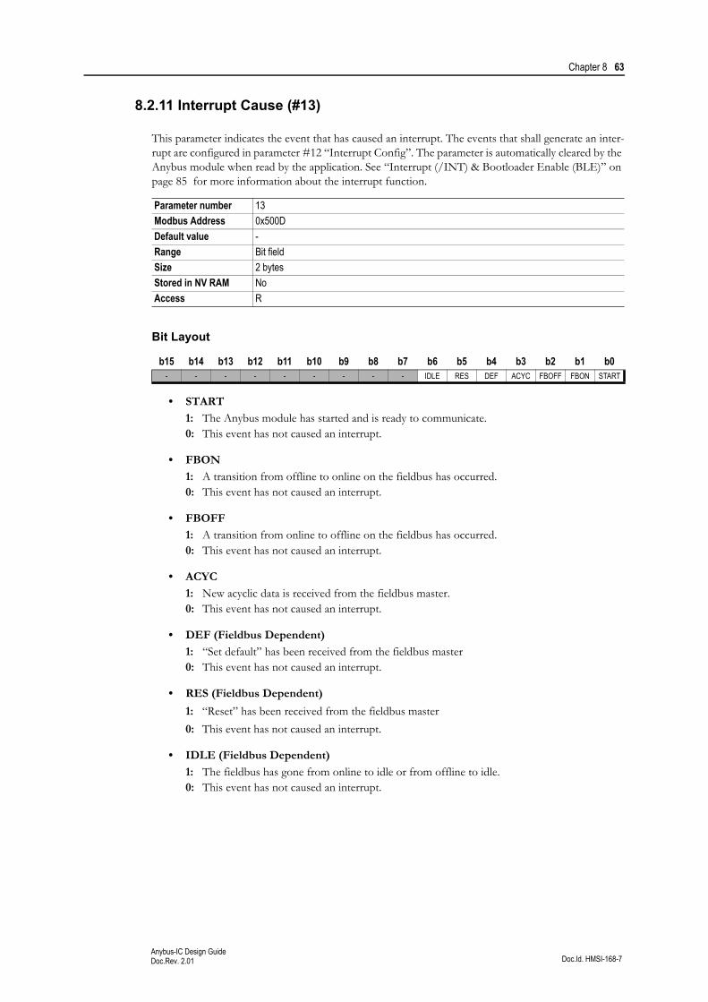
Chapter 8 63
Doc.Id. HMSI-168-7Anybus-IC Design GuideDoc.Rev. 2.01
8.2.11 Interrupt Cause (#13)
This parameter indicates the event that has caused an interrupt. The events that shall generate an inter-rupt are configured in parameter #12 “Interrupt Config”. The parameter is automatically cleared by the Anybus module when read by the application. See “Interrupt (/INT) & Bootloader Enable (BLE)” on page 85 for more information about the interrupt function.
Bit Layout
• START1: The Anybus module has started and is ready to communicate.0: This event has not caused an interrupt.
• FBON1: A transition from offline to online on the fieldbus has occurred.0: This event has not caused an interrupt.
• FBOFF1: A transition from online to offline on the fieldbus has occurred.0: This event has not caused an interrupt.
• ACYC
1: New acyclic data is received from the fieldbus master.0: This event has not caused an interrupt.
• DEF (Fieldbus Dependent)1: “Set default” has been received from the fieldbus master0: This event has not caused an interrupt.
• RES (Fieldbus Dependent)
1: “Reset” has been received from the fieldbus master
0: This event has not caused an interrupt.
• IDLE (Fieldbus Dependent)
1: The fieldbus has gone from online to idle or from offline to idle. 0: This event has not caused an interrupt.
Parameter number 13
Modbus Address 0x500D
Default value -
Range Bit field
Size 2 bytes
Stored in NV RAM No
Access R
b15 b14 b13 b12 b11 b10 b9 b8 b7 b6 b5 b4 b3 b2 b1 b0- - - - - - - - - IDLE RES DEF ACYC FBOFF FBON START
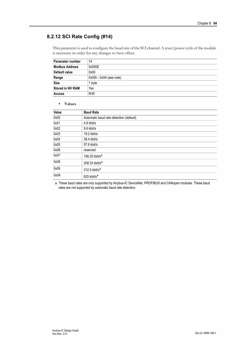
Chapter 8 64
Doc.Id. HMSI-168-7Anybus-IC Design GuideDoc.Rev. 2.01
8.2.12 SCI Rate Config (#14)
This parameter is used to configure the baud rate of the SCI channel. A reset/power cycle of the module is necessary in order for any changes to have effect.
• Values
Parameter number 14
Modbus Address 0x500E
Default value 0x00
Range 0x00h - 0x0A (see note)
Size 1 byte
Stored in NV RAM Yes
Access R/W
Value Baud Rate
0x00 Automatic baud rate detection (default)
0x01 4.8 kbit/s
0x02 9.6 kbit/s
0x03 19.2 kbit/s
0x04 38.4 kbit/s
0x05 57.6 kbit/s
0x06 reserved
0x07 156.25 kbit/sa
a. These baud rates are only supported by Anybus-IC DeviceNet, PROFIBUS and CANopen modules. These baud rates are not supported by automatic baud rate detection.
0x08 208.33 kbit/sa
0x09 312.5 kbit/sa
0x0A 625 kbit/sa
Chapter 8 65
Doc.Id. HMSI-168-7Anybus-IC Design GuideDoc.Rev. 2.01
8.2.13 SCI Rate Actual (#15)
This parameter returns is the actual baud rate of the SCI channel.
• Values
Parameter number 15
Modbus Address 0x500F
Default value -
Range 0x00 - 0x05 (see note)
Size 1 byte
Stored in NV RAM No
Access R
Value Baud Rate
0x00 Baud rate not set
0x01 4.8 kbit/s
0x02 9.6 kbit/s
0x03 19.2 kbit/s
0x04 38.4 kbit/s
0x05 57.6 kbit/s
0x06 reserved
0x07 156.25 kbit/sa
a. These baud rates are only supported by Anybus-IC DeviceNet, PROFIBUS and CANopen modules. These baud rates are not supported by automatic baud rate detection.
0x08 208.33 kbit/sa
0x09 312.5 kbit/sa
0x0A 625 kbit/sa
Chapter 8 66
Doc.Id. HMSI-168-7Anybus-IC Design GuideDoc.Rev. 2.01
8.2.14 SCI Settings Config (#16)
This parameter is used to configure the port settings of the SCI channel. A reset/power cycle of the module is necessary in order for any changes to have effect.
This parameter has no effect when automatic baud rate detection is enabled.
Bit Layout
• PAR2
1: Enable Parity
0: Disable Parity
• PAR1
(This bit has no effect if parity is disabled, see above)
1: Odd Parity
0: Even Parity
Parameter number 16
Modbus Address 0x5010
Default value 0x00
Range Bit field
Size 1 byte
Stored in NV RAM Yes
Access R/W
b7 b6 b5 b4 b3 b2 b1 b0- - - - - - PAR1 PAR2
Chapter 8 67
Doc.Id. HMSI-168-7Anybus-IC Design GuideDoc.Rev. 2.01
8.2.15 SCI Settings Actual (#17)
This parameter returns the actual port settings for the SCI channel. If automatic baud rate detection is enabled, the detected port settings are present in this parameter.
Bit Layout
• PAR2
1: Enable Parity
0: Disable Parity
• PAR1
(This bit has no effect if parity is disabled, see above)
1: Odd Parity
0: Even Parity
Parameter number 17
Modbus Address 0x5011
Default value -
Range Bit field
Size 1 byte
Stored in NV RAM No
Access R
b7 b6 b5 b4 b3 b2 b1 b0- - - - - - PAR1 PAR2
Chapter 8 68
Doc.Id. HMSI-168-7Anybus-IC Design GuideDoc.Rev. 2.01
8.2.16 MIF Rate Config (#18)
This parameter is used to configure the baud rate of the MIF interface. A reset/power cycle of the mod-ule is necessary in order for any changes to have effect.
Note: Automatic baud rate detection is not supported on this interface.
• Values
Note: Additional baud rates may be available on certain Anybus implementations. For more informa-tion, consult each separate fieldbus appendix.
Parameter number 18
Modbus Address 0x5012
Default value 0x04
Range 0x01 - 0x05 (see note)
Size 1 byte
Stored in NV RAM Yes
Access R/W
Value Baud Rate
0x01 4.8 kbit/s
0x02 9.6 kbit/s
0x03 19.2 kbit/s
0x04 38.4 kbit/s (default)
0x05 57.6 kbit/s
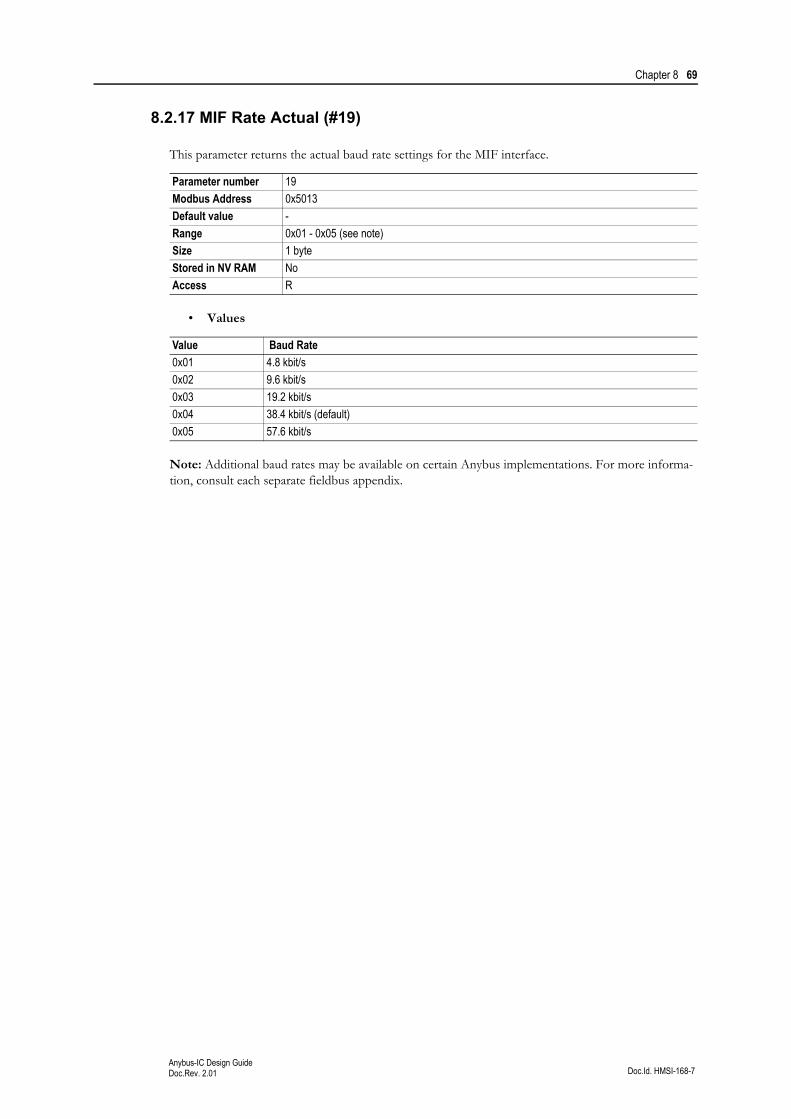
Chapter 8 69
Doc.Id. HMSI-168-7Anybus-IC Design GuideDoc.Rev. 2.01
8.2.17 MIF Rate Actual (#19)
This parameter returns the actual baud rate settings for the MIF interface.
• Values
Note: Additional baud rates may be available on certain Anybus implementations. For more informa-tion, consult each separate fieldbus appendix.
Parameter number 19
Modbus Address 0x5013
Default value -
Range 0x01 - 0x05 (see note)
Size 1 byte
Stored in NV RAM No
Access R
Value Baud Rate
0x01 4.8 kbit/s
0x02 9.6 kbit/s
0x03 19.2 kbit/s
0x04 38.4 kbit/s (default)
0x05 57.6 kbit/s
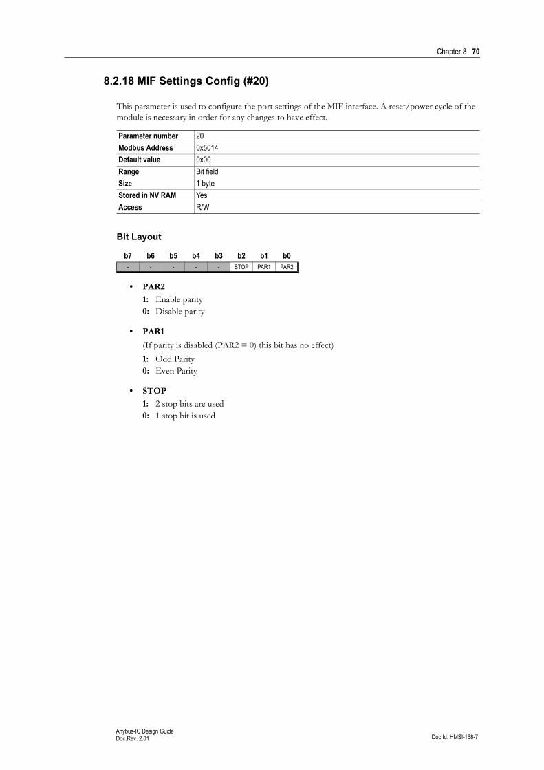
Chapter 8 70
Doc.Id. HMSI-168-7Anybus-IC Design GuideDoc.Rev. 2.01
8.2.18 MIF Settings Config (#20)
This parameter is used to configure the port settings of the MIF interface. A reset/power cycle of the module is necessary in order for any changes to have effect.
Bit Layout
• PAR21: Enable parity0: Disable parity
• PAR1
(If parity is disabled (PAR2 = 0) this bit has no effect)
1: Odd Parity0: Even Parity
• STOP
1: 2 stop bits are used0: 1 stop bit is used
Parameter number 20
Modbus Address 0x5014
Default value 0x00
Range Bit field
Size 1 byte
Stored in NV RAM Yes
Access R/W
b7 b6 b5 b4 b3 b2 b1 b0- - - - - STOP PAR1 PAR2
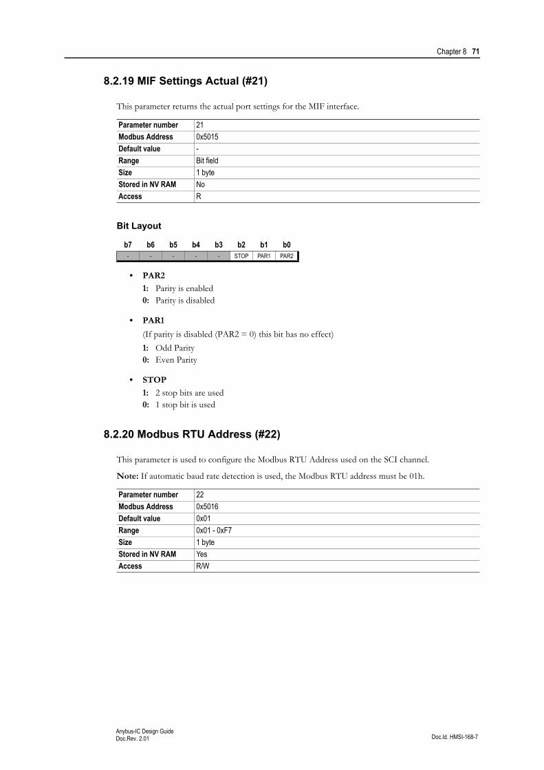
Chapter 8 71
Doc.Id. HMSI-168-7Anybus-IC Design GuideDoc.Rev. 2.01
8.2.19 MIF Settings Actual (#21)
This parameter returns the actual port settings for the MIF interface.
Bit Layout
• PAR21: Parity is enabled0: Parity is disabled
• PAR1
(If parity is disabled (PAR2 = 0) this bit has no effect)
1: Odd Parity0: Even Parity
• STOP
1: 2 stop bits are used0: 1 stop bit is used
8.2.20 Modbus RTU Address (#22)
This parameter is used to configure the Modbus RTU Address used on the SCI channel.
Note: If automatic baud rate detection is used, the Modbus RTU address must be 01h.
Parameter number 21
Modbus Address 0x5015
Default value -
Range Bit field
Size 1 byte
Stored in NV RAM No
Access R
b7 b6 b5 b4 b3 b2 b1 b0- - - - - STOP PAR1 PAR2
Parameter number 22
Modbus Address 0x5016
Default value 0x01
Range 0x01 - 0xF7
Size 1 byte
Stored in NV RAM Yes
Access R/W
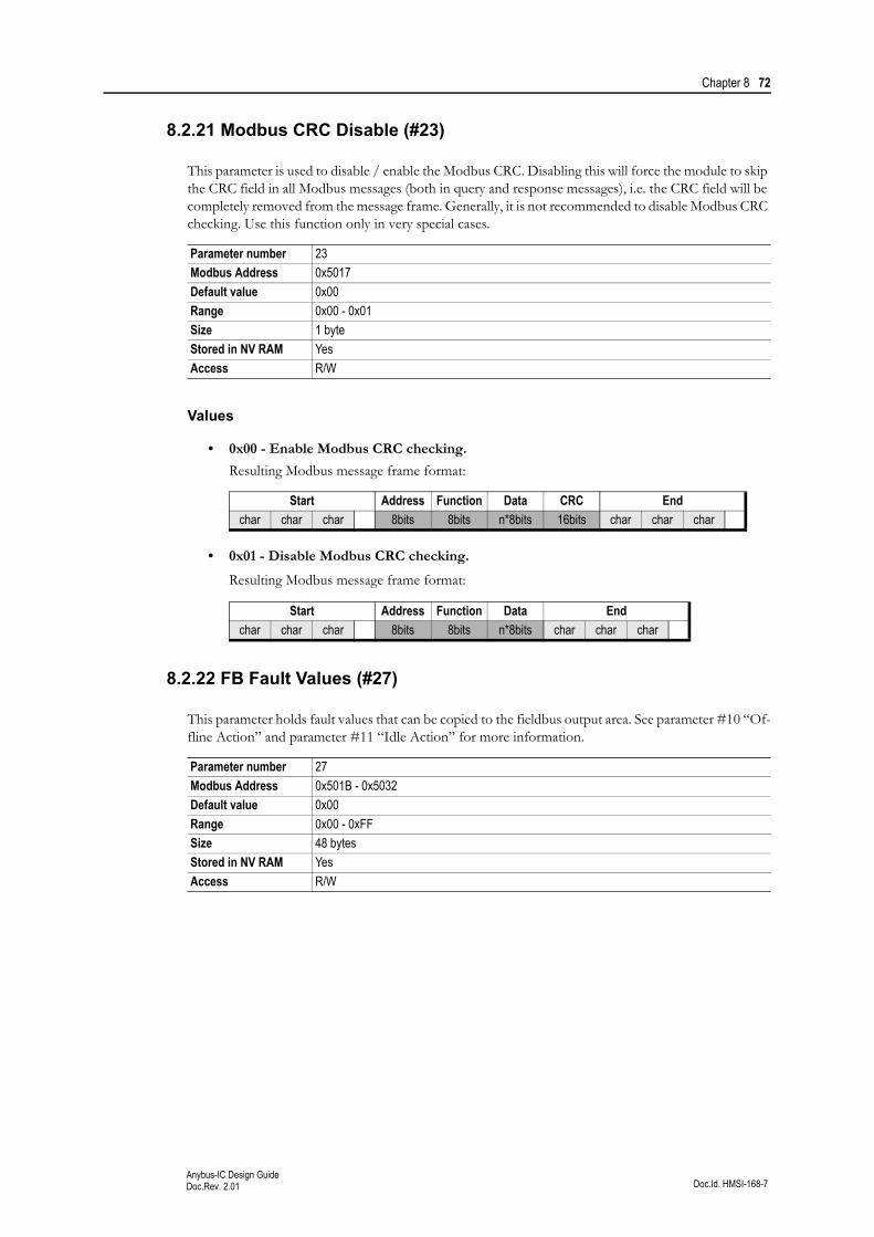
Chapter 8 72
Doc.Id. HMSI-168-7Anybus-IC Design GuideDoc.Rev. 2.01
8.2.21 Modbus CRC Disable (#23)
This parameter is used to disable / enable the Modbus CRC. Disabling this will force the module to skip the CRC field in all Modbus messages (both in query and response messages), i.e. the CRC field will be completely removed from the message frame. Generally, it is not recommended to disable Modbus CRC checking. Use this function only in very special cases.
Values
• 0x00 - Enable Modbus CRC checking.
Resulting Modbus message frame format:
• 0x01 - Disable Modbus CRC checking.
Resulting Modbus message frame format:
8.2.22 FB Fault Values (#27)
This parameter holds fault values that can be copied to the fieldbus output area. See parameter #10 “Of-fline Action” and parameter #11 “Idle Action” for more information.
Parameter number 23
Modbus Address 0x5017
Default value 0x00
Range 0x00 - 0x01
Size 1 byte
Stored in NV RAM Yes
Access R/W
Start Address Function Data CRC End
char char char 8bits 8bits n*8bits 16bits char char char
Start Address Function Data End
char char char 8bits 8bits n*8bits char char char
Parameter number 27
Modbus Address 0x501B - 0x5032
Default value 0x00
Range 0x00 - 0xFF
Size 48 bytes
Stored in NV RAM Yes
Access R/W
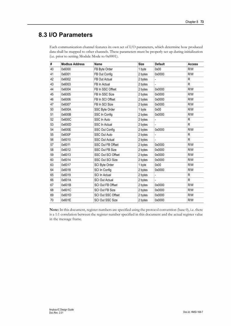
Chapter 8 73
Doc.Id. HMSI-168-7Anybus-IC Design GuideDoc.Rev. 2.01
8.3 I/O Parameters
Each communication channel features its own set of I/O parameters, which determine how produced data shall be mapped to other channels. These parameters must be properly set up during initialization (i.e. prior to setting Module Mode to 0x0001).
Note: In this document, register numbers are specified using the protocol convention (base 0), i.e. there is a 1:1 correlation between the register number specified in this document and the actual register value in the message frame.
# Modbus Address Name Size Default Access
40 0x6000 FB Byte Order 1 byte 0x00 R/W
41 0x6001 FB Out Config 2 bytes 0x0000 R/W
42 0x6002 FB Out Actual 2 bytes - R
43 0x6003 FB In Actual 2 bytes - R
44 0x6004 FB In SSC Offset 2 bytes 0x0000 R/W
45 0x6005 FB In SSC Size 2 bytes 0x0000 R/W
46 0x6006 FB In SCI Offset 2 bytes 0x0000 R/W
47 0x6007 FB In SCI Size 2 bytes 0x0000 R/W
50 0x600A SSC Byte Order 1 byte 0x00 R/W
51 0x600B SSC In Config 2 bytes 0x0000 R/W
52 0x600C SSC In Auto 2 bytes - R
53 0x600D SSC In Actual 2 bytes - R
54 0x600E SSC Out Config 2 bytes 0x0000 R/W
55 0x600F SSC Out Auto 2 bytes - R
56 0x6010 SSC Out Actual 2 bytes - R
57 0x6011 SSC Out FB Offset 2 bytes 0x0000 R/W
58 0x6012 SSC Out FB Size 2 bytes 0x0000 R/W
59 0x6013 SSC Out SCI Offset 2 bytes 0x0000 R/W
60 0x6014 SSC Out SCI Size 2 bytes 0x0000 R/W
63 0x6017 SCI Byte Order 1 byte 0x00 R/W
64 0x6018 SCI In Config 2 bytes 0x0000 R/W
65 0x6019 SCI In Actual 2 bytes - R
66 0x601A SCI Out Actual 2 bytes - R
67 0x601B SCI Out FB Offset 2 bytes 0x0000 R/W
68 0x601C SCI Out FB Size 2 bytes 0x0000 R/W
69 0x601D SCI Out SSC Offset 2 bytes 0x0000 R/W
70 0x601E SCI Out SSC Size 2 bytes 0x0000 R/W
Chapter 8 74
Doc.Id. HMSI-168-7Anybus-IC Design GuideDoc.Rev. 2.01
8.3.1 FB Byte Order (#40)
This parameter determines if the bytes in the fieldbus I/O area shall be byte swapped or not relative to the other I/O areas.
Note that in order for this function to work properly, the I/O length must be a multiple of 16 bits / 2 bytes.
Example:
If data is mapped from the “FB Output area” to the “SSC Output area”, parameter #40 “FB Byte Order” is 0x00, and parameter #50 “SSC Byte Order” is 0x01, the data written to the “FB Output area” will be swapped when it reaches the “SSC Output area”. If the byte order param-eters has the same value for both areas, no swap will be made.
Note: Both the FB Input area and the FB Output area are affected by this parameter.
Values
• 0x00
Do not swap bytes in the fieldbus I/O area.
• 0x01
Swap bytes in the fieldbus I/O area.
8.3.2 FB Out Config (#41)
This parameter configures the size of the FB Out area. The size is specified in bytes.
Parameter number 40
Modbus Address 0x6000
Default value 0x00
Range 0x00 - 0x01
Size 1 byte
Stored in NV RAM Yes
Access R/W
Parameter number 41
Modbus Address 0x6001
Default value 0x0000
Range 0x0000 - 0x0090h
Size 2 bytes
Stored in NV RAM Yes
Access R/W
Chapter 8 75
Doc.Id. HMSI-168-7Anybus-IC Design GuideDoc.Rev. 2.01
8.3.3 FB Out Actual (#42)
This parameter holds the actual size of the FB Out area after initialization. The size is specified in bytes.
8.3.4 FB In Actual (#43)
This parameter holds the actual size of the FB In area after initialization. The value of this parameter is calculated using parameter #45 “FB In SSC Size” and parameter #47 “FB In SCI Size”. The size is spec-ified in bytes.
8.3.5 FB In SSC Offset (#44)
This parameter is used to set the source location for the SSC Input -> Fieldbus Input mapping.
Parameter number 42
Modbus Address 0x6002
Modbus Address
Default value -
Range 0x0000 - 0x0090
Size 2 bytes
Stored in NV RAM No
Access R
Parameter number 43
Modbus Address 0x6003
Default value -
Range 0x0000 - 0x0090
Size 2 bytes
Stored in NV RAM No
Access R
Parameter number 44
Modbus Address 0x6004
Default value 0x0000
Range 0x0000h - 0x000F
Size 2 bytes
Stored in NV RAM Yes
Access R/W
Chapter 8 76
Doc.Id. HMSI-168-7Anybus-IC Design GuideDoc.Rev. 2.01
8.3.6 FB In SSC Size (#45)
This parameter is used to specify how many bytes that will be mapped from the SSC Input area to the Fieldbus Input area.
8.3.7 FB In SCI Offset (#46)
This parameter is used to set the source location for the SCI Input -> Fieldbus Input mapping.
8.3.8 FB In SCI Size (#47)
This parameter is used to specify how many bytes that will be mapped from the SCI Input area to the Fieldbus Input area.
Parameter number 45
Modbus Address 0x6005
Default value 0x0000
Range 0x0000 - 0x0010
Size 2 bytes
Stored in NV RAM Yes
Access R/W
Parameter number 46
Modbus Address 0x6006
Default value 0x0000
Range 0x0000 - 0x007F
Size 2 bytes
Stored in NV RAM Yes
Access R/W
Parameter number 47
Modbus Address 0x6007
Default value 0x0000
Range 0x0000 - 0x0080
Size 2 bytes
Stored in NV RAM Yes
Access R/W
Chapter 8 77
Doc.Id. HMSI-168-7Anybus-IC Design GuideDoc.Rev. 2.01
8.3.9 SSC Byte Order (#50)
This parameter determines if the bytes in the SSC I/O area shall be swapped or not relative to the other I/O areas.
Example
If data is mapped from the “SSC Input area” to the “FB Input area”, parameter #50 “SSC Byte Order” is 0x00, and parameter #40 “FB Byte Order” is 0x01, the data written to the “SSC Input area” will be swapped when it reaches the “FB Input area”. If the byte order parameters has the same value for both areas, no swap will be made.
Note that in order for this function to work properly, the I/O length must be a multiple of 16 bits / 2 bytes.
Note: The entire SSC I/O area is affected by the state of this parameter no matter of the contents.
Values
• 0x00
Do not swap bytes in the SSC I/O area.
• 0x01
Swap bytes in the SSC I/O area.
8.3.10 SSC In Config (#51)
This parameter is used to configure the total size of the SSC In area (the FB specific input byte is not included in this size). The size is specified in bytes.
In order for the value of this parameter to be valid after initialization, the SSCI bit in parameter #8 “Con-figuration Bits” must be set.
Parameter number 50
Modbus Address 0x600A
Default value 0x00
Range 0x00 - 0x01
Size 1 byte
Stored in NV RAM Yes
Access R/W
Parameter number 51
Modbus Address 0x600B
Default value 0x0000
Range 0x0000 - 0x0010
Size 2 bytes
Stored in NV RAM Yes
Access R/W
Chapter 8 78
Doc.Id. HMSI-168-7Anybus-IC Design GuideDoc.Rev. 2.01
8.3.11 SSC In Auto (#52)
This parameter returns the automatically configured size of the SSC In area (the FB specific input byte is not included in this size). The size is specified in bytes.
In order for the value of this parameter to be valid after initialization, the SSCI bit in parameter #8 “Con-figuration Bits” must be cleared.
8.3.12 SSC In Actual (#53)
This parameter returns the actual size of the SSC In area after initialization (the fieldbus specific input byte is not included in this size). The size is specified in bytes.
8.3.13 SSC Out Config (#54)
This parameter is used to configure the total size of the SSC Out area (the FB specific output byte is not included in this size). The size is specified in bytes.
In order for the value of this parameter to be valid after initialization, the SSCO bit in parameter #8 “Configuration Bits” must be set.
Parameter number 52
Modbus Address 0x600C
Default value -
Range 0x0000 - 0x0010
Size 2 bytes
Stored in NV RAM No
Access R
Parameter number 53
Modbus Address 0x600D
Default value -
Range 0x0000 - 0x0010
Size 2 bytes
Stored in NV RAM No
Access R
Parameter number 54
Modbus Address 0x600E
Default value 0x0000
Range 0x0000 - 0x0010
Size 2 bytes
Stored in NV RAM Yes
Access R/W
Chapter 8 79
Doc.Id. HMSI-168-7Anybus-IC Design GuideDoc.Rev. 2.01
8.3.14 SSC Out Auto (#55)
This parameter returns the automatically configured size of the SSC Out area (the FB specific output byte is not included in this size). The size is specified in bytes.
In order for the value of this parameter to be valid after initialization, the SSCO bit in parameter #8 “Configuration Bits” must be cleared.
8.3.15 SSC Out Actual (#56)
This parameter returns the actual size of the SSC Out area after initialization (the FB specific output byte is not included in this size). The size is specified in bytes.
8.3.16 SSC Out FB Offset (#57)
This parameter is used to set the source location for the Fieldbus Output -> SSC output mapping.
Parameter number 55
Modbus Address 0x600F
Default value -
Range 0x0000 - 0x0010
Size 2 bytes
Stored in NV RAM No
Access R
Parameter number 56
Modbus Address 0x6010
Default value -
Range 0x0000 - 0x0010
Size 2 bytes
Stored in NV RAM No
Access R
Parameter number 57
Modbus Address 0x6011
Default value 0x0000
Range 0x0000 - 0x008F
Size 2 bytes
Stored in NV RAM Yes
Access R/W
Chapter 8 80
Doc.Id. HMSI-168-7Anybus-IC Design GuideDoc.Rev. 2.01
8.3.17 SSC Out FB Size (#58)
This parameter is used to specify how many bytes that will be mapped from the Fieldbus Output area to the SSC Output area.
8.3.18 SSC Out SCI Offset (#59)
This parameter is used to set the source location for the SCI Input -> SSC Output mapping.
8.3.19 SSC Out SCI Size (#60)
This parameter is used to specify how many bytes that will be mapped from the SCI Input area to the SSC Output area.
Parameter number 58
Modbus Address 0x6012
Default value 0x0000
Range 0x0000 - 0x0010
Size 2 bytes
Stored in NV RAM Yes
Access R/W
Parameter number 59
Modbus Address 0x6013
Default value 0x0000
Range 0x0000 - 0x007F
Size 2 bytes
Stored in NV RAM Yes
Access R/W
Parameter number 60
Modbus Address 0x6014
Default value 0x0000
Range 0x0000 - 0x0010
Size 2 bytes
Stored in NV RAM Yes
Access R/W
Chapter 8 81
Doc.Id. HMSI-168-7Anybus-IC Design GuideDoc.Rev. 2.01
8.3.20 SCI Byte Order (#63)
This parameter determines if the bytes in the SCI I/O area shall be swapped or not relative to the other I/O areas.
Example:
If data is mapped from the “SCI Input area” to the “FB Input area”, parameter #63 “SCI Byte Order” is 0x00, and parameter #40 “FB Byte Order” is 0x01, the data written to the “SCI Input area” will be swapped when it reaches the “FB Input area”. If the byte order parameters has the same value for both areas, no swap will be made.
Note that in order for this function to work properly, the I/O length must be a multiple of 16 bits / 2 bytes.
Note: The entire SCI I/O area is affected by the state of this parameter no matter of the contents.
Values
• 0x00
Do not swap bytes in the SCI I/O area.
• 0x01
Swap bytes in the SCI I/O area.
8.3.21 SCI In Config (#64)
This parameter configures the size of the SCI In area. The size is specified in bytes.
Parameter number 63
Modbus Address 0x6017
Default value 0x00
Range 0x00 - 0x01
Size 1 byte
Stored in NV RAM Yes
Access R/W
Parameter number 64
Modbus Address 0x6018
Default value 0x0000
Range 0x0000 - 0x0080
Size 2 bytes
Stored in NV RAM Yes
Access R/W
Chapter 8 82
Doc.Id. HMSI-168-7Anybus-IC Design GuideDoc.Rev. 2.01
8.3.22 SCI In Actual (#65)
This parameter holds the actual size of the SCI In area after initialization. The size is specified in bytes.
8.3.23 SCI Out Actual (#66)
This parameter holds the actual size of the SCI Out area after initialization. The value of this parameter is calculated using parameter #68 “SCI Out FB Size” and parameter #70 “SCI Out SSC Size”. The size is specified in bytes.
8.3.24 SCI Out FB Offset (#67)
This parameter is used to set the source location for the Fieldbus Output -> SCI Output mapping.
8.3.25 SCI Out FB Size (#68)
This parameter is used to specify how many bytes that will be mapped from the Fieldbus Output area to the SCI Output area.
Parameter number 65
Modbus Address 0x6019
Default value -
Range 0x0000 - 0x0080
Size 2 bytes
Stored in NV RAM No
Access R
Parameter number 66
Modbus Address 0x601A
Default value -
Range 0x0000 - 0x0080
Size 2 bytes
Stored in NV RAM No
Access R
Parameter number 67
Modbus Address 0x601B
Default value 0x0000
Range 0x0000 - 0x007F
Size 2 bytes
Stored in NV RAM Yes
Access R/W
Parameter number 68
Modbus Address 0x601C
Default value 0x0000
Range 0x0000 - 0x0080
Size 2 bytes
Stored in NV RAM Yes
Access R/W
Chapter 8 83
Doc.Id. HMSI-168-7Anybus-IC Design GuideDoc.Rev. 2.01
8.3.26 SCI Out SSC Offset (#69)
This parameter is used to set the source location for the SSC Input -> SCI Output mapping.
8.3.27 SCI Out SSC Size (#70)
This parameter is used to specify how many bytes that will be mapped from the SSC Input area to the SCI Output area.
Parameter number 69
Modbus Address 0x601D
Default value 0x0000
Range 0x0000 - 0x000F
Size 2 bytes
Stored in NV RAM Yes
Access R/W
Parameter number 70
Modbus Address 0x601E
Default value 0x0000
Range 0x0000 - 0x0010
Size 2 bytes
Stored in NV RAM Yes
Access R/W

Chapter 8 84
Doc.Id. HMSI-168-7Anybus-IC Design GuideDoc.Rev. 2.01
8.4 Fieldbus Specific Parameters
Consult each separate fieldbus appendix for further information.
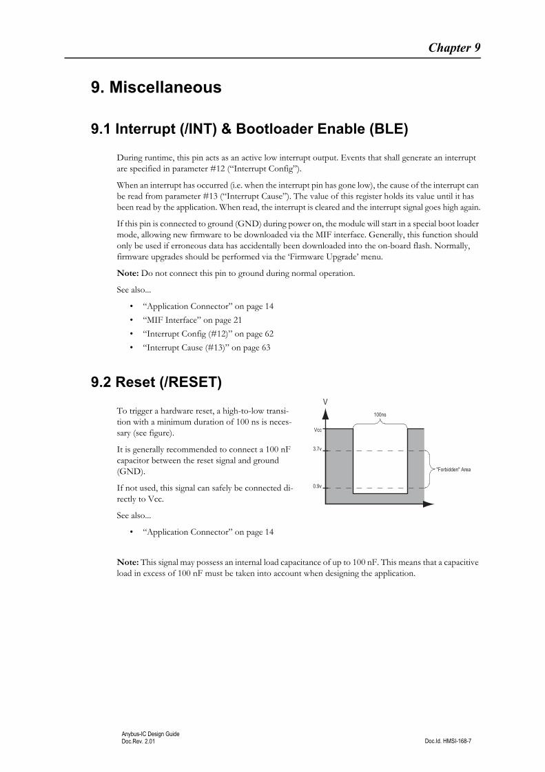
Doc.Id. HMSI-168-7Anybus-IC Design GuideDoc.Rev. 2.01
Chapter 9
9. Miscellaneous
9.1 Interrupt (/INT) & Bootloader Enable (BLE)
During runtime, this pin acts as an active low interrupt output. Events that shall generate an interrupt are specified in parameter #12 (“Interrupt Config”).
When an interrupt has occurred (i.e. when the interrupt pin has gone low), the cause of the interrupt can be read from parameter #13 (“Interrupt Cause”). The value of this register holds its value until it has been read by the application. When read, the interrupt is cleared and the interrupt signal goes high again.
If this pin is connected to ground (GND) during power on, the module will start in a special boot loader mode, allowing new firmware to be downloaded via the MIF interface. Generally, this function should only be used if erroneous data has accidentally been downloaded into the on-board flash. Normally, firmware upgrades should be performed via the ‘Firmware Upgrade’ menu.
Note: Do not connect this pin to ground during normal operation.
See also...
• “Application Connector” on page 14
• “MIF Interface” on page 21
• “Interrupt Config (#12)” on page 62
• “Interrupt Cause (#13)” on page 63
9.2 Reset (/RESET)
To trigger a hardware reset, a high-to-low transi-tion with a minimum duration of 100 ns is neces-sary (see figure).
It is generally recommended to connect a 100 nF capacitor between the reset signal and ground (GND).
If not used, this signal can safely be connected di-rectly to Vcc.
See also...
• “Application Connector” on page 14
Note: This signal may possess an internal load capacitance of up to 100 nF. This means that a capacitive load in excess of 100 nF must be taken into account when designing the application.
3.7v
Vcc
0.9v
V100ns
"Forbidden" Area
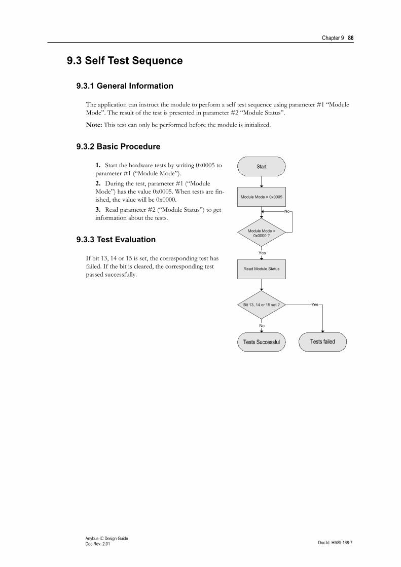
Chapter 9 86
Doc.Id. HMSI-168-7Anybus-IC Design GuideDoc.Rev. 2.01
9.3 Self Test Sequence
9.3.1 General Information
The application can instruct the module to perform a self test sequence using parameter #1 “Module Mode”. The result of the test is presented in parameter #2 “Module Status”.
Note: This test can only be performed before the module is initialized.
9.3.2 Basic Procedure
1. Start the hardware tests by writing 0x0005 to parameter #1 (“Module Mode”).
2. During the test, parameter #1 (“Module Mode”) has the value 0x0005. When tests are fin-ished, the value will be 0x0000.
3. Read parameter #2 (“Module Status”) to get information about the tests.
9.3.3 Test Evaluation
If bit 13, 14 or 15 is set, the corresponding test has failed. If the bit is cleared, the corresponding test passed successfully.
Start
Tests Successful
No
Yes
Tests failed
Yes
No
Module Mode = 0x0005
Module Mode =0x0000 ?
Read Module Status
Bit 13, 14 or 15 set ?
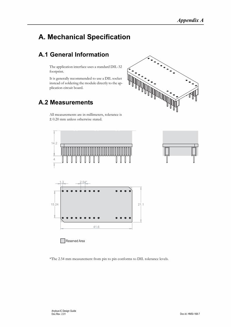
Doc.Id. HMSI-168-7Anybus-IC Design GuideDoc.Rev. 2.01
Appendix A
A. Mechanical Specification
A.1 General Information
The application interface uses a standard DIL-32 footprint.
It is generally recommended to use a DIL socket instead of soldering the module directly to the ap-plication circuit board.
A.2 Measurements
All measurements are in millimeters, tolerance is ± 0.20 mm unless otherwise stated.
*The 2.54 mm measurement from pin to pin conforms to DIL tolerance levels.
4
14.2
41.6
21.115.24
1.3 2.54*
Reserved Area

Doc.Id. HMSI-168-7Anybus-IC Design GuideDoc.Rev. 2.01
Appendix B
B. Firmware Upgrade
The firmware of the module can be updated using the HMS firmware download utility.
For more information, contact HMS technical support.
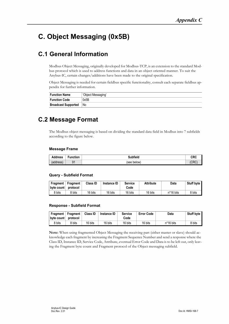
Doc.Id. HMSI-168-7Anybus-IC Design GuideDoc.Rev. 2.01
Appendix C
C. Object Messaging (0x5B)
C.1 General Information
Modbus Object Messaging, originally developed for Modbus-TCP, is an extension to the standard Mod-bus protocol which is used to address functions and data in an object oriented manner. To suit the Anybus-IC, certain changes/additions have been made to the original specification.
Object Messaging is needed for certain fieldbus specific functionality, consult each separate fieldbus ap-pendix for further information.
C.2 Message Format
The Modbus object messaging is based on dividing the standard data field in Modbus into 7 subfields according to the figure below.
Message Frame
Query - Subfield Format
Response - Subfield Format
Note: When using fragmented Object Messaging the receiving part (either master or slave) should ac-knowledge each fragment by increasing the Fragment Sequence Number and send a response where the Class ID, Instance ID, Service Code, Attribute, eventual Error Code and Data is to be left out, only leav-ing the Fragment byte count and Fragment protocol of the Object messaging subfield.
Function Name ‘Object Messaging’
Function Code 0x5B
Broadcast Supported No
Address Function Subfield CRC
(address) 91 (see below) (CRC)
Fragmentbyte count
Fragmentprotocol
Class ID Instance ID Service Code
Attribute Data Stuff byte
8 bits 8 bits 16 bits 16 bits 16 bits 16 bits n*16 bits 8 bits
Fragmentbyte count
Fragmentprotocol
Class ID Instance ID Service Code
Error Code Data Stuff byte
8 bits 8 bits 16 bits 16 bits 16 bits 16 bits n*16 bits 8 bits
Appendix C 90
Doc.Id. HMSI-168-7Anybus-IC Design GuideDoc.Rev. 2.01
C.3 Subfield Contents
C.3.1 Fragment Byte Count
This field contains the number of bytes of the current object message (itself excluded).
The maximum number of bytes is 197.
Note: If a stuff byte is added at the end of the message, it is not included in the Fragment byte count.
C.3.2 Fragment Protocol
This field is used when sending fragmented messages. The bits are described below.
• FIPI - Fragment In Process Indicator
1: This message is a fragment of a fragmented message.
0: This message is not fragmented.
• LFI - Last Fragment Indicator
1: This is the last fragment in a fragmented message.
0: This not the last fragment in a fragmented message.
• FSN - Fragment Sequence Number
This is a counter counting from 0002 to 1112. Each fragment in a fragmented message has a se-quential number in this field.
C.3.3 Class ID
ID of the object class associated with the service.
C.3.4 Instance ID
ID of the instance associated with the service.
Bit 7 Bit 6 Bit 5 Bit 4 Bit 3 Bit 2 Bit 1 Bit 0
FSN - - - LFI FIPI
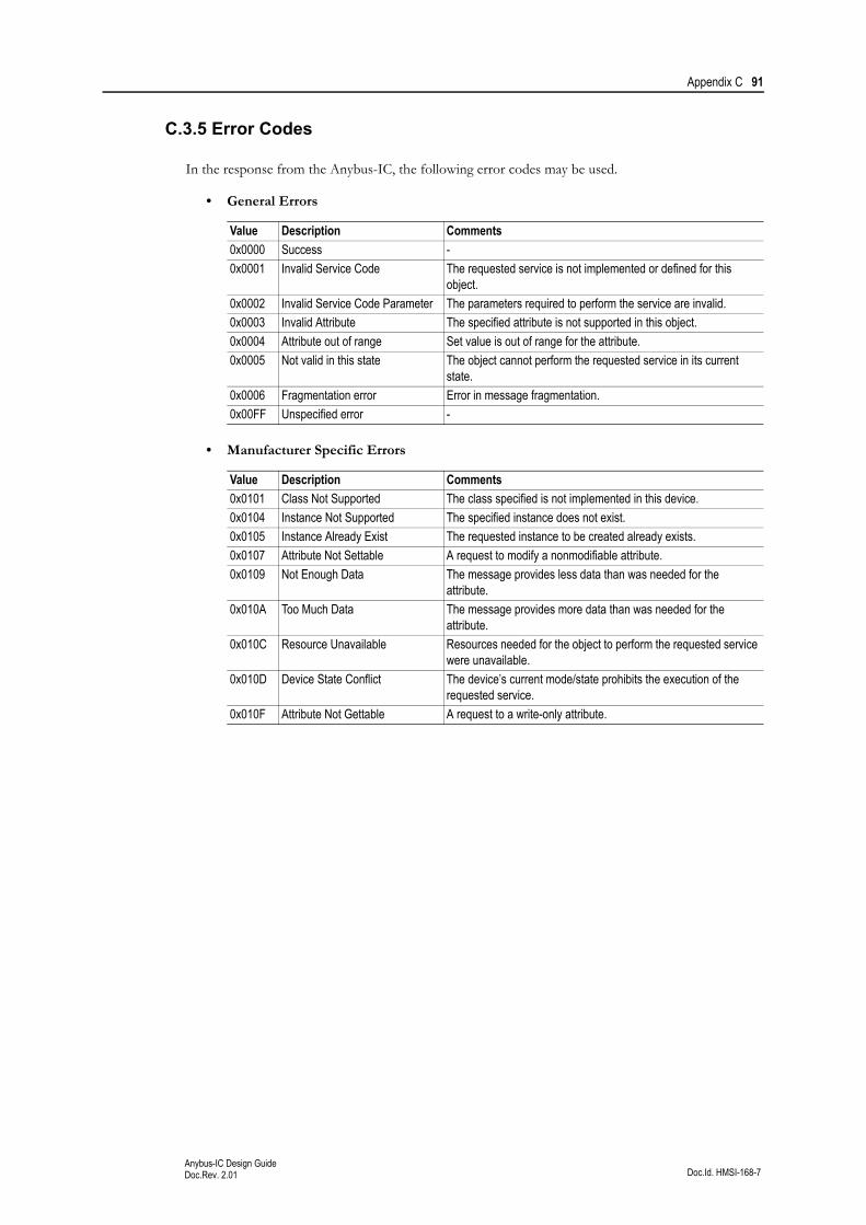
Appendix C 91
Doc.Id. HMSI-168-7Anybus-IC Design GuideDoc.Rev. 2.01
C.3.5 Error Codes
In the response from the Anybus-IC, the following error codes may be used.
• General Errors
• Manufacturer Specific Errors
Value Description Comments
0x0000 Success -
0x0001 Invalid Service Code The requested service is not implemented or defined for this object.
0x0002 Invalid Service Code Parameter The parameters required to perform the service are invalid.
0x0003 Invalid Attribute The specified attribute is not supported in this object.
0x0004 Attribute out of range Set value is out of range for the attribute.
0x0005 Not valid in this state The object cannot perform the requested service in its current state.
0x0006 Fragmentation error Error in message fragmentation.
0x00FF Unspecified error -
Value Description Comments
0x0101 Class Not Supported The class specified is not implemented in this device.
0x0104 Instance Not Supported The specified instance does not exist.
0x0105 Instance Already Exist The requested instance to be created already exists.
0x0107 Attribute Not Settable A request to modify a nonmodifiable attribute.
0x0109 Not Enough Data The message provides less data than was needed for the attribute.
0x010A Too Much Data The message provides more data than was needed for the attribute.
0x010C Resource Unavailable Resources needed for the object to perform the requested service were unavailable.
0x010D Device State Conflict The device’s current mode/state prohibits the execution of the requested service.
0x010F Attribute Not Gettable A request to a write-only attribute.
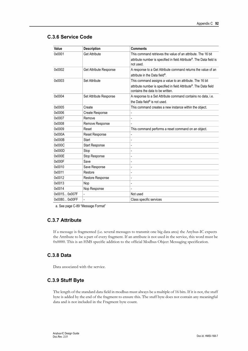
Appendix C 92
Doc.Id. HMSI-168-7Anybus-IC Design GuideDoc.Rev. 2.01
C.3.6 Service Code
C.3.7 Attribute
If a message is fragmented (i.e. several messages to transmit one big data area) the Anybus-IC expects the Attribute to be a part of every fragment. If an attribute is not used in the service, this word must be 0x0000. This is an HMS specific addition to the official Modbus Object Messaging specification.
C.3.8 Data
Data associated with the service.
C.3.9 Stuff Byte
The length of the standard data field in modbus must always be a multiple of 16 bits. If it is not, the stuff byte is added by the end of the fragment to ensure this. The stuff byte does not contain any meaningful data and is not included in the Fragment byte count.
Value Description Comments
0x0001 Get Attribute This command retrieves the value of an attribute. The 16 bit
attribute number is specified in field Attributea. The Data field is not used.
a. See page C-89 “Message Format”
0x0002 Get Attribute Response A response to a Get Attribute command returns the value of an
attribute in the Data fielda.
0x0003 Set Attribute This command assigns a value to an attribute. The 16 bit
attribute number is specified in field Attributea. The Data field contains the data to be written.
0x0004 Set Attribute Response A response to a Set Attribute command contains no data, i.e.
the Data fielda is not used.
0x0005 Create This command creates a new instance within the object.
0x0006 Create Response -
0x0007 Remove -
0x0008 Remove Response -
0x0009 Reset This command performs a reset command on an object.
0x000A Reset Response -
0x000B Start -
0x000C Start Response -
0x000D Stop -
0x000E Stop Response -
0x000F Save -
0x0010 Save Response -
0x0011 Restore -
0x0012 Restore Response -
0x0013 Nop -
0x0014 Nop Response -
0x0015... 0x007F - Not used
0x0080... 0x00FF - Class specific services

Doc.Id. HMSI-168-7Anybus-IC Design GuideDoc.Rev. 2.01
Appendix D
D. Technical Specification
Note: The properties specified in this chapter applies to all Anybus-IC modules unless otherwise stated. Any deviations from what is stated herein is specified separately in each network appendix.
D.1 Environmental
Temperature
Operating: -40 to +85 °C (-40 to 185°F)Storage: -40 to +85 °C (-40 to 185°F)
(Tests performed according to IEC 68-2-1 and IEC 68-2-2)
Wave Soldering
Temperature: 320°CVelocity: 10 mm/s
Humidity
5 to 95% noncondensing (tests performed according to IEC 68-2-30)
D.2 Power Supply
Supply Voltage
The module requires a regulated +5 V ± 5% DC power supply.
The power supply rise time (0.1 VCC to 0.9 VCC) must be less than 50 ms.
Power Consumption
The maximum power consumption may vary. Please consult each separate fieldbus appendix.
Isolation
Isolation distances between application and network (according to EN 60950-1; Pollution degree 2; Ma-terial Group IIIb):
Protective Earth & Shielding
PE-requirements are fieldbus dependent. Please consult the separate fieldbus appendix for details.
Isolation BarrierWorking Voltage/Transient Voltage Distance
Creepage Clearance External Internal
Application to Networka
a. Valid for all modules except Ethernet modules which utilize a customer supplied transformer.
250 V/2500 V 250 V/2500 V 2.5 mm 0.4 mm
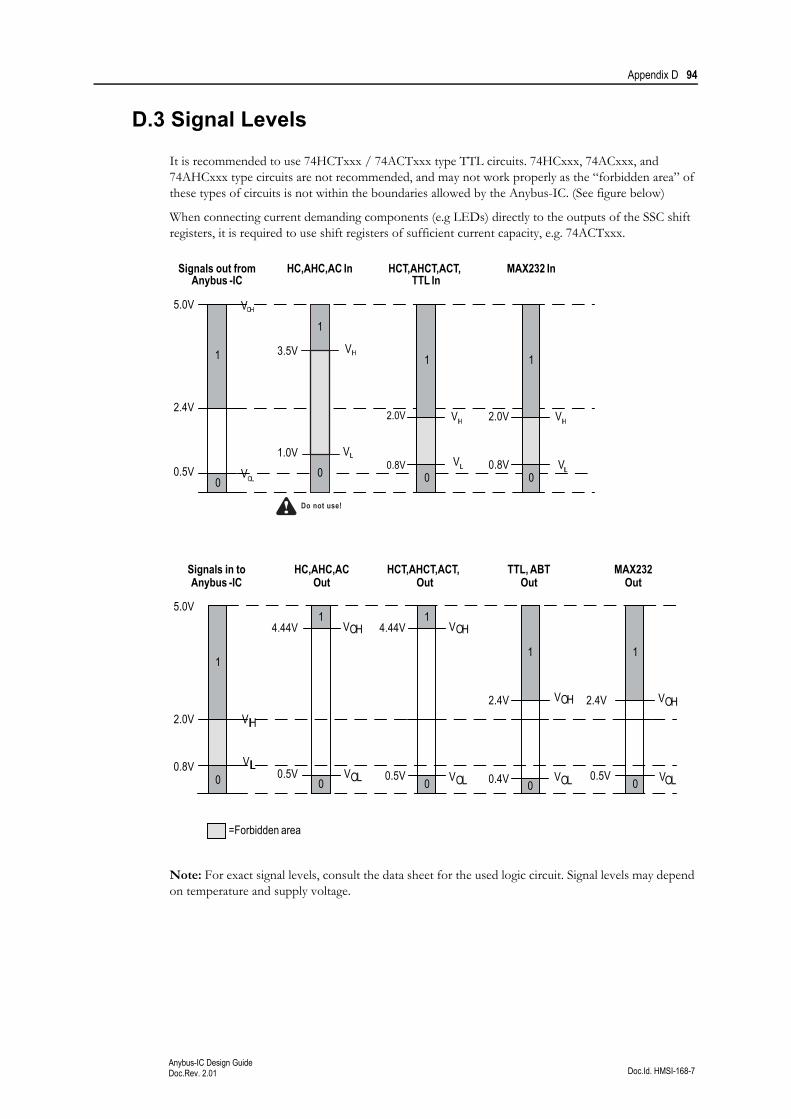
Appendix D 94
Doc.Id. HMSI-168-7Anybus-IC Design GuideDoc.Rev. 2.01
D.3 Signal Levels
It is recommended to use 74HCTxxx / 74ACTxxx type TTL circuits. 74HCxxx, 74ACxxx, and 74AHCxxx type circuits are not recommended, and may not work properly as the “forbidden area” of these types of circuits is not within the boundaries allowed by the Anybus-IC. (See figure below)
When connecting current demanding components (e.g LEDs) directly to the outputs of the SSC shift registers, it is required to use shift registers of sufficient current capacity, e.g. 74ACTxxx.
Note: For exact signal levels, consult the data sheet for the used logic circuit. Signal levels may depend on temperature and supply voltage.
MAX232 In
1
0
2.0V
0.8V V IL
V IH
HCT,AHCT,ACT, TTL In
1
0
2.0V
0.8V
V IH
V IL
HC,AHC,AC In
3.5V
1
1.0V 0
V IL
V IH
Signals out from Anybus -IC
2.4V
1
0.5V 0
5.0V
V OL
VOH
Signals in to Anybus -IC
2.0V
1
0.8V 0
5.0V
V IH
V IL
HC,AHC,AC Out
4.44V 1
0.5V 0
V OH
V OL
1
0
HCT,AHCT,ACT, Out
0.5V
4.44V V OH
V OL
TTL, ABT Out
1
0 0.4V
2.4V V OH
V OL
MAX232 Out
1
0 0.5V
2.4V V OH
V OL
=Forbidden area
Do not use!
Appendix D 95
Doc.Id. HMSI-168-7Anybus-IC Design GuideDoc.Rev. 2.01
D.4 Regulatory Compliance
D.4.1 Fieldbus Certification
All Anybus-IC modules are precertified and found to comply with each fieldbus standard. Please note that although the module itself has been precertified, the final product may still require recertification depending on the fieldbus standard.
This precertification is valid under the following conditions:
• Standard fieldbus connectors
• No fieldbus specific initialization parameters
• Nonmodified device description file (i.e. ‘.GSD’ or ‘.EDS’)
Any changes to the conditions above invalidates the precertification. For more information, consult each fieldbus standard specification and/or contact HMS.
D.4.2 EMC Compliance (CE)
Generally, Anybus-IC products are certified according to the European CE standard unless otherwise stated. It is however important to note that although the Anybus module itself is certified, the final prod-uct may still require recertification depending on the application.
D.4.3 UL/cUL-Certificate
The Anybus-IC modules are UL/cUL recognized for the US (NRAQ2) and Canada (NRAQ8) accord-ing to UL508, “Programmable Controller”.