Embed Size (px)
Citation preview
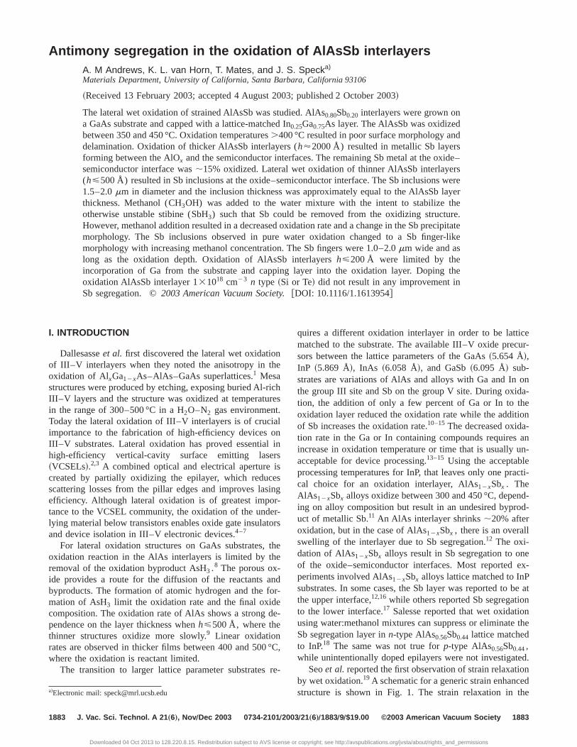
Antimony segregation in the oxidation of AlAsSb interlayersA. M Andrews, K. L. van Horn, T. Mates, and J. S. Speck Citation: J. Vac. Sci. Technol. A 21, 1883 (2003); doi: 10.1116/1.1613954 View online: http://dx.doi.org/10.1116/1.1613954 View Table of Contents: http://avspublications.org/resource/1/JVTAD6/v21/i6 Published by the AVS: Science & Technology of Materials, Interfaces, and Processing Related ArticlesStructural and electrical characterization of InN, InGaN, and p-InGaN grown by metal-modulated epitaxy J. Vac. Sci. Technol. B 31, 03C104 (2013) LOGISTIC FUNCTION PROFILE FIT: A least-squares program for fitting interface profiles to an extended logisticfunction J. Vac. Sci. Technol. A 30, 051101 (2012) Probing temporal evolution of extreme ultraviolet assisted contamination on Ru mirror by x-ray photoelectronspectroscopy J. Vac. Sci. Technol. B 30, 021601 (2012) Thermal-vacuum stability of the surface oxide complex on Cu J. Vac. Sci. Technol. A 29, 053001 (2011) Segregation and interlayer relaxation at the NiPd(111) surface J. Vac. Sci. Technol. A 29, 011015 (2011) Additional information on J. Vac. Sci. Technol. AJournal Homepage: http://avspublications.org/jvsta Journal Information: http://avspublications.org/jvsta/about/about_the_journal Top downloads: http://avspublications.org/jvsta/top_20_most_downloaded Information for Authors: http://avspublications.org/jvsta/authors/information_for_contributors
Downloaded 04 Oct 2013 to 128.220.8.15. Redistribution subject to AVS license or copyright; see http://avspublications.org/jvsta/about/rights_and_permissions
Antimony segregation in the oxidation of AlAsSb interlayersA. M Andrews, K. L. van Horn, T. Mates, and J. S. Specka)
Materials Department, University of California, Santa Barbara, California 93106
~Received 13 February 2003; accepted 4 August 2003; published 2 October 2003!
The lateral wet oxidation of strained AlAsSb was studied. AlAs0.80Sb0.20 interlayers were grown ona GaAs substrate and capped with a lattice-matched In0.25Ga0.75As layer. The AlAsSb was oxidizedbetween 350 and 450 °C. Oxidation temperatures.400 °C resulted in poor surface morphology anddelamination. Oxidation of thicker AlAsSb interlayers (h'2000 Å) resulted in metallic Sb layersforming between the AlOx and the semiconductor interfaces. The remaining Sb metal at the oxide–semiconductor interface was;15% oxidized. Lateral wet oxidation of thinner AlAsSb interlayers(h<500 Å) resulted in Sb inclusions at the oxide–semiconductor interface. The Sb inclusions were1.5–2.0mm in diameter and the inclusion thickness was approximately equal to the AlAsSb layerthickness. Methanol (CH3OH) was added to the water mixture with the intent to stabilize theotherwise unstable stibine (SbH3) such that Sb could be removed from the oxidizing structure.However, methanol addition resulted in a decreased oxidation rate and a change in the Sb precipitatemorphology. The Sb inclusions observed in pure water oxidation changed to a Sb finger-likemorphology with increasing methanol concentration. The Sb fingers were 1.0–2.0mm wide and aslong as the oxidation depth. Oxidation of AlAsSb interlayersh<200 Å were limited by theincorporation of Ga from the substrate and capping layer into the oxidation layer. Doping theoxidation AlAsSb interlayer 131018 cm23 n type ~Si or Te! did not result in any improvement inSb segregation. ©2003 American Vacuum Society.@DOI: 10.1116/1.1613954#
nhe
icre
alonl irsisesinr-
erto
the
noree
°
r
ceur-
ona-e
ion-an
un-
cti-
d-d-
eex-
be atnnthe
ed.onedhe
I. INTRODUCTION
Dallesasseet al. first discovered the lateral wet oxidatioof III–V interlayers when they noted the anisotropy in toxidation of AlxGa12xAs–AlAs–GaAs superlattices.1 Mesastructures were produced by etching, exposing buried Al-rIII–V layers and the structure was oxidized at temperatuin the range of 300–500 °C in a H2O–N2 gas environment.Today the lateral oxidation of III–V interlayers is of cruciimportance to the fabrication of high-efficiency devicesIII–V substrates. Lateral oxidation has proved essentiahigh-efficiency vertical-cavity surface emitting lase~VCSELs!.2,3 A combined optical and electrical aperturecreated by partially oxidizing the epilayer, which reducscattering losses from the pillar edges and improves laefficiency. Although lateral oxidation is of greatest impotance to the VCSEL community, the oxidation of the undlying material below transistors enables oxide gate insulaand device isolation in III–V electronic devices.4–7
For lateral oxidation structures on GaAs substrates,oxidation reaction in the AlAs interlayers is limited by thremoval of the oxidation byproduct AsH3.8 The porous ox-ide provides a route for the diffusion of the reactants abyproducts. The formation of atomic hydrogen and the fmation of AsH3 limit the oxidation rate and the final oxidcomposition. The oxidation rate of AlAs shows a strong dpendence on the layer thickness whenh<500 Å, where thethinner structures oxidize more slowly.9 Linear oxidationrates are observed in thicker films between 400 and 500where the oxidation is reactant limited.
The transition to larger lattice parameter substrates
a!Electronic mail: [email protected]
1883 J. Vac. Sci. Technol. A 21 „6…, Nov ÕDec 2003 0734-2101Õ200
Downloaded 04 Oct 2013 to 128.220.8.15. Redistribution subject to AVS license o
hs
n
sg
-rs
e
d-
-
C,
e-
quires a different oxidation interlayer in order to be lattimatched to the substrate. The available III–V oxide precsors between the lattice parameters of the GaAs~5.654 Å!,InP ~5.869 Å!, InAs ~6.058 Å!, and GaSb~6.095 Å! sub-strates are variations of AlAs and alloys with Ga and Inthe group III site and Sb on the group V site. During oxidtion, the addition of only a few percent of Ga or In to thoxidation layer reduced the oxidation rate while the additof Sb increases the oxidation rate.10–15The decreased oxidation rate in the Ga or In containing compounds requiresincrease in oxidation temperature or time that is usuallyacceptable for device processing.13–15 Using the acceptableprocessing temperatures for InP, that leaves only one pracal choice for an oxidation interlayer, AlAs12xSbx . TheAlAs12xSbx alloys oxidize between 300 and 450 °C, depening on alloy composition but result in an undesired byprouct of metallic Sb.11 An AlAs interlayer shrinks;20% afteroxidation, but in the case of AlAs12xSbx , there is an overallswelling of the interlayer due to Sb segregation.12 The oxi-dation of AlAs12xSbx alloys result in Sb segregation to onof the oxide–semiconductor interfaces. Most reportedperiments involved AlAs12xSbx alloys lattice matched to InPsubstrates. In some cases, the Sb layer was reported tothe upper interface,12,16 while others reported Sb segregatioto the lower interface.17 Salesse reported that wet oxidatiousing water:methanol mixtures can suppress or eliminateSb segregation layer inn-type AlAs0.56Sb0.44 lattice matchedto InP.18 The same was not true forp-type AlAs0.56Sb0.44,while unintentionally doped epilayers were not investigat
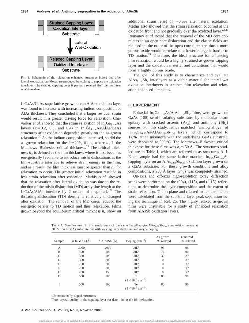
Seoet al. reported the first observation of strain relaxatiby wet oxidation.19 A schematic for a generic strain enhancstructure is shown in Fig. 1. The strain relaxation in t
18833Õ21„6…Õ1883Õ9Õ$19.00 ©2003 American Vacuum Society
r copyright; see http://avspublications.org/jvsta/about/rights_and_permissions
eo
aa
owhe
ethm
i
re
dth
.the
r-areoretog
nguld
ateetx-
m
of
te,ical-–I.
lloy.n
oftersus-
wnion
afatiye
1884 Andrews et al. : Antimony segregation in the oxidation of AlAsSb 1884
InGaAs/GaAs superlattice grown on an AlAs oxidation laywas found to increase with increasing indium compositionAlAs thickness. They concluded that a larger residual strwould result in a greater driving force for relaxation. Chvarkaret al. showed that the strain relaxation of InxGa12xAslayers (x50.2, 0.3, and 0.4! in InxGa12xAs/AlAs/GaAsstructures after oxidation depended greatly on the as-grrelaxation.20 As the indium composition increased, so did tas-grown relaxation for theh'20hc films, wherehc is theMatthews–Blakeslee critical thickness.21 The critical thick-nesshc is defined as the film thickness where it first becomenergetically favorable to introduce misfit dislocations atfilm-substrate interface to relieve strain energy in the filand as a result, the film thickness must be greater thanhc forrelaxation to occur. The greater initial relaxation resultedless strain relaxation after oxidation. Mathiset al. showedthat the relaxation after lateral oxidation was due to theduction of the misfit dislocation~MD! array line length at theInGaAs/AlAs interface by 2 orders of magnitude.22 Thethreading dislocation~TD! density is relatively unchangeafter oxidation. The removal of the MD cores reducedenergetic barrier to TD motion and thus relaxation. Filmgrown beyond the equilibrium critical thicknesshc show an
FIG. 1. Schematic of the relaxation enhanced structures before andlateral wet oxidation. Mesas are produced by etching to expose the oxidinterlayer. The strained capping layer is partially relaxed after the interlais wet oxidized.
J. Vac. Sci. Technol. A, Vol. 21, No. 6, Nov ÕDec 2003
Downloaded 04 Oct 2013 to 128.220.8.15. Redistribution subject to AVS license o
rr
in-
n
se,
n
-
es
additional strain relief of;0.5% after lateral oxidationMathis also showed that the strain relaxation occurred atoxidation front and not gradually over the oxidized layer.22,23
Romanovet al. noted that the removal of the MD core corelates to an open core dislocation and the elastic fieldsreduced on the order of the open core diameter, thus a mporous oxide would correlate to a lower energetic barrierTD motion.24 Therefore, the ideal structure for enhancinfilm relaxation would be a highly strained as-grown cappilayer and the oxidation material and conditions that woform a highly porous oxide.
The goal of this study is to characterize and evaluAlAs12xSbx interlayers as a viable material for lateral woxidation interlayers in strained film relaxation and relaation enhanced templates.
II. EXPERIMENT
Epitaxial InxGa12xAs/AlAs12xSbx films were grown onGaAs ~100! semi-insulating substrates by molecular beaepitaxy with cracked arsenic (As2) and antimony (Sb2)sources. For this study, lattice matched ‘‘analog alloys’’In0.25Ga0.75As/AlAs0.80Sb0.20 layers, which correspond to1.8% lattice mismatch with the underlying GaAs substrawere deposited at 500 °C. The Matthews–Blakeslee critthickness for these films washc'50 Å. The structures studied are in Table I, which are referred to as structures AEach sample had the same lattice matched In0.25Ga0.75Ascapping layer on an AlAs0.80Sb0.20 oxidation layer grown ona GaAs substrate. For these growth conditions and acompositions, a 250 Å layer (5hc) was completely strained
On-axis and off-axis high-resolution x-ray diffractioscans were performed on the~004!, ~115!, and (1̄1̄5) reflec-tions to determine the layer composition and the extentstrain relaxation. The in-plane and relaxed lattice paramewere calculated from the substrate-layer peak separationing the technique in Ref. 25. The highly relaxed as-grofilms were unsuitable for a study of enhanced relaxatfrom AlAsSb oxidation layers.
teronr
TABLE I. Samples used in this study were of the same In0.25Ga0.75As/AlAs0.80Sb0.20 composition grown at500 °C on a GaAs substrate but with varying layer thickness andn-type doping.
Sample h InGaAs ~Å! h AlAsSb ~Å! Doping ~cm23!As grown
;% relaxedOxidized
;% relaxed
A 3000 2000 UIDa 98 98B 500 500 UIDa 76 90C 350 200 UIDa 30 Xb
D 300 200 UIDa 0 Xb
E 250 200 UIDa 0 Xb
F 200 200 UIDa 0 Xb
G 200 150 UIDa 0 Xb
H 500 500 Si(131018 cm23)
80 90
I 500 500 Te(131018 cm23)
80 90
aUnintentionally doped structures.bPoor crystal quality in the capping layer for determining the film relaxation.
r copyright; see http://avspublications.org/jvsta/about/rights_and_permissions
as 1:0 in
1885 Andrews et al. : Antimony segregation in the oxidation of AlAsSb 1885
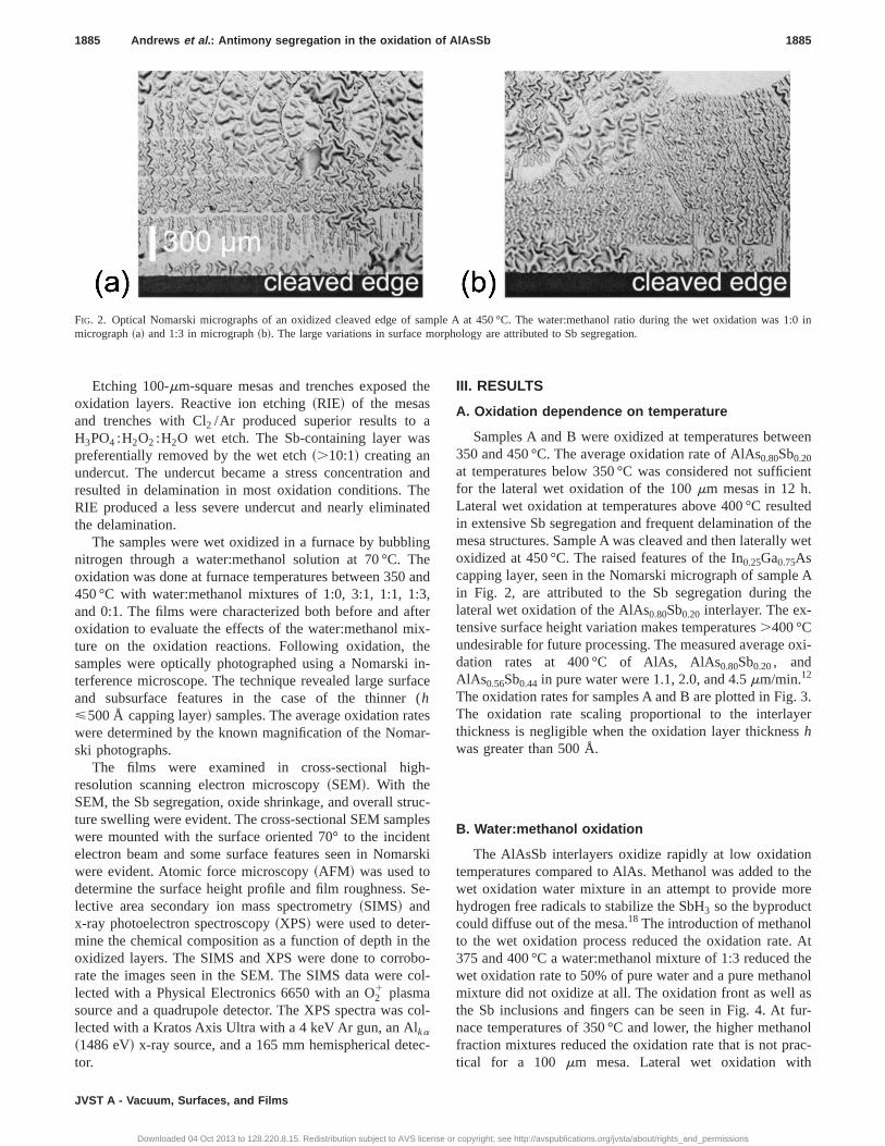
FIG. 2. Optical Nomarski micrographs of an oxidized cleaved edge of sample A at 450 °C. The water:methanol ratio during the wet oxidation wmicrograph~a! and 1:3 in micrograph~b!. The large variations in surface morphology are attributed to Sb segregation.
th
as
aheat
inha
:3ftix
heinfa(
esar
h
ruplenar
S
-thboco
c
ec
een
ient
ltedthewet
e Athe
oxi-
. 3.ers
nthere
lAt
thenols
fur-nol
ac-
Etching 100-mm-square mesas and trenches exposedoxidation layers. Reactive ion etching~RIE! of the mesasand trenches with Cl2 /Ar produced superior results toH3PO4:H2O2:H2O wet etch. The Sb-containing layer wapreferentially removed by the wet etch~.10:1! creating anundercut. The undercut became a stress concentrationresulted in delamination in most oxidation conditions. TRIE produced a less severe undercut and nearly eliminthe delamination.
The samples were wet oxidized in a furnace by bubblnitrogen through a water:methanol solution at 70 °C. Toxidation was done at furnace temperatures between 350450 °C with water:methanol mixtures of 1:0, 3:1, 1:1, 1and 0:1. The films were characterized both before and aoxidation to evaluate the effects of the water:methanol mture on the oxidation reactions. Following oxidation, tsamples were optically photographed using a Nomarskiterference microscope. The technique revealed large surand subsurface features in the case of the thinnerh<500 Å capping layer! samples. The average oxidation ratwere determined by the known magnification of the Nomski photographs.
The films were examined in cross-sectional higresolution scanning electron microscopy~SEM!. With theSEM, the Sb segregation, oxide shrinkage, and overall stture swelling were evident. The cross-sectional SEM samwere mounted with the surface oriented 70° to the incidelectron beam and some surface features seen in Nomwere evident. Atomic force microscopy~AFM! was used todetermine the surface height profile and film roughness.lective area secondary ion mass spectrometry~SIMS! andx-ray photoelectron spectroscopy~XPS! were used to determine the chemical composition as a function of depth inoxidized layers. The SIMS and XPS were done to corrorate the images seen in the SEM. The SIMS data werelected with a Physical Electronics 6650 with an O2
1 plasmasource and a quadrupole detector. The XPS spectra waslected with a Kratos Axis Ultra with a 4 keV Ar gun, an Alka
~1486 eV! x-ray source, and a 165 mm hemispherical dettor.
JVST A - Vacuum, Surfaces, and Films
Downloaded 04 Oct 2013 to 128.220.8.15. Redistribution subject to AVS license o
e
nd
ed
gend,er-
-ce
-
-
c-estski
e-
e-l-
ol-
-
III. RESULTS
A. Oxidation dependence on temperature
Samples A and B were oxidized at temperatures betw350 and 450 °C. The average oxidation rate of AlAs0.80Sb0.20
at temperatures below 350 °C was considered not sufficfor the lateral wet oxidation of the 100mm mesas in 12 h.Lateral wet oxidation at temperatures above 400 °C resuin extensive Sb segregation and frequent delamination ofmesa structures. Sample A was cleaved and then laterallyoxidized at 450 °C. The raised features of the In0.25Ga0.75Ascapping layer, seen in the Nomarski micrograph of samplin Fig. 2, are attributed to the Sb segregation duringlateral wet oxidation of the AlAs0.80Sb0.20 interlayer. The ex-tensive surface height variation makes temperatures.400 °Cundesirable for future processing. The measured averagedation rates at 400 °C of AlAs, AlAs0.80Sb0.20, andAlAs0.56Sb0.44 in pure water were 1.1, 2.0, and 4.5mm/min.12
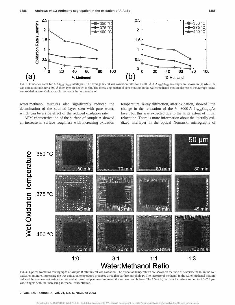
The oxidation rates for samples A and B are plotted in FigThe oxidation rate scaling proportional to the interlaythickness is negligible when the oxidation layer thickneshwas greater than 500 Å.
B. Water:methanol oxidation
The AlAsSb interlayers oxidize rapidly at low oxidatiotemperatures compared to AlAs. Methanol was added towet oxidation water mixture in an attempt to provide mohydrogen free radicals to stabilize the SbH3 so the byproductcould diffuse out of the mesa.18 The introduction of methanoto the wet oxidation process reduced the oxidation rate.375 and 400 °C a water:methanol mixture of 1:3 reducedwet oxidation rate to 50% of pure water and a pure methamixture did not oxidize at all. The oxidation front as well athe Sb inclusions and fingers can be seen in Fig. 4. Atnace temperatures of 350 °C and lower, the higher methafraction mixtures reduced the oxidation rate that is not prtical for a 100 mm mesa. Lateral wet oxidation with
r copyright; see http://avspublications.org/jvsta/about/rights_and_permissions
lateral
1886 Andrews et al. : Antimony segregation in the oxidation of AlAsSb 1886
FIG. 3. Oxidation rates for AlAs0.80Sb0.20 interlayers. The average lateral wet oxidation rates for a 2000 Å AlAs0.80Sb0.20 interlayer are shown in~a! while thewet oxidation rates for a 500 Å interlayer are shown in~b!. The increasing methanol concentration in the water:methanol mixture decreases the averagewet oxidation rate. Oxidation did not occur in pure methanol.
thte
etio
le
tialxi-of
water:methanol mixtures also significantly reduceddelamination of the strained layer seen with pure wawhich can be a side effect of the reduced oxidation rate.
AFM characterization of the surface of sample A showan increase in surface roughness with increasing oxida
J. Vac. Sci. Technol. A, Vol. 21, No. 6, Nov ÕDec 2003
Downloaded 04 Oct 2013 to 128.220.8.15. Redistribution subject to AVS license o
er,
dn
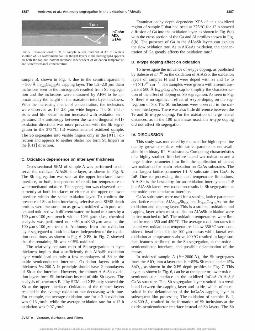
temperature. X-ray diffraction, after oxidation, showed littchange in the relaxation of theh53000 Å In0.25Ga0.75Aslayer, but this was expected due to the large extent of inirelaxation. There is more information about the laterally odized interlayer in the optical Nomarski micrographs
in the wnol
FIG. 4. Optical Nomarski micrographs of sample B after lateral wet oxidation. The oxidation temperatures are shown vs the ratio of water:methanoletoxidation mixture. Increasing the wet oxidation temperature produced a rougher surface morphology. The increase of methanol in the water:methamixturereduced the average wet oxidation rate and at lower temperatures improved the surface morphology. The 1.5–2.0mm diam inclusions turned to 1.5–2.0mmwide fingers with the increasing methanol concentration.
r copyright; see http://avspublications.org/jvsta/about/rights_and_permissions
t
gapssn
-m
rele
s
ob5wo
coe
heepway a
ided
yenhe
arsahtherm
h
eded
ig.ainn-
tos--ig.
-xi-the
al
neil-icsa
alheis
ns,Pat
eter
ndereim-
foron-tsur-de–the
s
ise–b/eakre-in–I,
heSb
a
tu
1887 Andrews et al. : Antimony segregation in the oxidation of AlAsSb 1887
sample B, shown in Fig. 4, due to the semitransparenh5500 Å In0.25Ga0.75As capping layer. The 1.5–2.0mm diaminclusions seen in the micrograph resulted from Sb segretion and the inclusions were measured by AFM to beproximately the height of the oxidation interlayer thickneWith the increasing methanol concentration, the inclusiowere observed as 1.0–2.0mm wide fingers. The Sb inclusions and film delamination increased with oxidation teperature. The anisotropy between the two orthogonal^011&oxidation directions was more prevalent with the Sb seggation in the 375 °C 1:3 water:methanol oxidized sampThe Sb segregates into visible fingers only in the@01̄1# di-rection and appears to neither blister nor form Sb fingerthe @011# direction.
C. Oxidation dependence on interlayer thickness
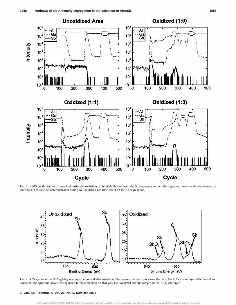
Cross-sectional SEM of sample A was performed toserve the oxidized AlAsSb interlayer, as shown in Fig.The Sb segregation was seen at the upper interface, lointerface, or both, independent of oxidation temperaturewater:methanol mixture. The segregation was observedcurrently at both interfaces or either at the upper or lowinterface within the same oxidation layer. To confirm tpresence of Sb at both interfaces, selective area SIMS dprofiles were measured on as-grown, oxidized with pureter, and oxidized with different water:methanol mixtures b100mm3100mm trench with a 10% gate~i.e., chemicalanalysis was performed on;30mm330mm area in the100mm3100mm trench!. Antimony from the oxidationlayer segregated to both interfaces independent of the oxtion conditions, as shown in Fig. 6. XPS, in Fig. 7, showthat the remaining Sb was;15% oxidized.
The relatively constant ratio of Sb segregation to lathickness implies that a sufficiently thin AlAsSb oxidatiolayer would lead to only a few monolayers of Sb at toxide–semiconductor interface. Oxidation layers withthicknessh<200 Å in principle should have 2 monolayeof Sb at the interface. However, the thinner AlAsSb oxidtion layers form Sb inclusions instead of thin Sb layers. Tanalysis of structures B–I by SEM and XPS only showedSb at the upper interface. Oxidation of the thinner layresulted in the average oxidation rate decreasing with tiFor example, the average oxidation rate fora 3 h oxidationwas 0.13mm/h, while the average oxidation rate for a 12oxidation was 0.07mm/h.
FIG. 5. Cross-sectional SEM of sample A wet oxidized at 375 °C withsolution of 3:1 water:methanol. Sb~bright layers in the micrograph! appearson both the top and bottom interface independent of oxidation temperaand water:methanol concentration.
JVST A - Vacuum, Surfaces, and Films
Downloaded 04 Oct 2013 to 128.220.8.15. Redistribution subject to AVS license o
a--.s
-
-.
in
-.errn-r
th-
a-
r
-eese.
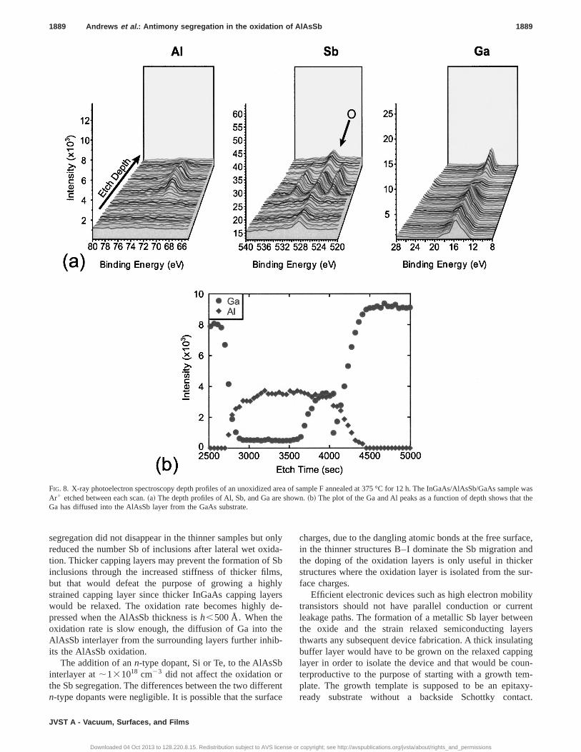
Examination by depth dependent XPS of an unoxidizregion of sample F that had been at 375 °C for 12 h showdiffusion of Ga into the oxidation layer, as shown in Fig. 8~a!with the cross section of the Ga and Al profiles shown in F8~b!. The presence of Ga in the AlAsSb layers can explthe slow oxidation rate. As in AlGaAs oxidation, the concetration of Ga greatly affects the oxidation rate.1
D. n-type doping affect on oxidation
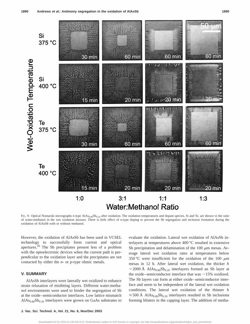
To investigate the influence ofn-type doping, as publishedby Salesseet al.,18 on the oxidation of AlAsSb, the oxidationlayers of samples H and I were doped with Si and Te;131018 cm23. The samples were grown with a semitranparent 500 Å In0.25Ga0.75As cap to simplify the characterization of the effect of doping on Sb segregation. As seen in F9, there is no significant effect ofn-type doping on the segregation of Sb. The Sb inclusions were observed in the odized interlayers. There was also little difference betweenTe and Sin-type doping. For the oxidation of large laterdistances, as in the 100mm mesas used, then-type dopingdid not affect Sb segregation.
IV. DISCUSSION
This study was motivated by the need for high crystalliquality growth templates with lattice parameters not avaable from binary III–V substrates. Competing characteristof a highly strained film before lateral wet oxidation andlarge lattice parameter film limit the application of laterwet oxidation for strain relaxation on GaAs substrates. Tnext largest lattice parameter III–V substrate after GaAsInP. Due to processing time and temperature limitatioAlAsSb is the best alloy for an oxidation interlayer on Inbut AlAsSb lateral wet oxidation results in Sb segregationthe oxide–semiconductor interface.
GaAs substrates were used for a starting lattice paramand lattice matched AlAs0.80Sb0.20 and In0.25Ga0.75As for theoxidation and capping layer. This is a strained oxidation acapping layer when most studies on AlAsSb oxidation wlattice matched to InP. The oxidation temperatures were lited between 350 and 450 °C. The average oxidation rateslateral wet oxidation at temperatures below 350 °C were csidered insufficient for the 100mm mesas while lateral weoxidation at temperatures above 400 °C resulted in largeface features attributed to the Sb segregation, at the oxisemiconductor interface, and possible delamination ofmesas.
In oxidized sample A (h52000 Å), the Sb segregatefrom the AlOx into a layer that is;85% Sb metal and;15%SbOx , as shown in the XPS depth profiles in Fig. 7. Thlayer, as shown in Fig. 6, can be at the upper or lower oxidsemiconductor interface in the oxidized InGaAs/AlAsSGaAs structure. This Sb segregation layer resulted in a wbond between the capping layer and oxide, which oftensulted in the delamination of the InGaAs capping layersubsequent film processing. The oxidation of samples Bh<500 Å, resulted in the formation of Sb inclusions at toxide–semiconductor interface instead of Sb layers. The
re
r copyright; see http://avspublications.org/jvsta/about/rights_and_permissions
onductor
ral wet
1888 Andrews et al. : Antimony segregation in the oxidation of AlAsSb 1888
FIG. 6. SIMS depth profiles of sample A. After the oxidation of the AlAsSb interlayer, the Sb segregates to both the upper and lower oxide–semicinterfaces. The ratio of water:methanol during wet oxidation has little effect on the Sb segregation.
FIG. 7. XPS spectra of the AlAs0.8Sb0.2 interlayer before and after oxidation. The unoxidized spectrum shows the Sb in the AlAsSb interlayer. After lateoxidation, the spectrum peaks corresponded to the remaining Sb that was 15% oxidized and the oxygen in the AlOx interlayer.
J. Vac. Sci. Technol. A, Vol. 21, No. 6, Nov ÕDec 2003
Downloaded 04 Oct 2013 to 128.220.8.15. Redistribution subject to AVS license or copyright; see http://avspublications.org/jvsta/about/rights_and_permissions
ample wasthe
1889 Andrews et al. : Antimony segregation in the oxidation of AlAsSb 1889
FIG. 8. X-ray photoelectron spectroscopy depth profiles of an unoxidized area of sample F annealed at 375 °C for 12 h. The InGaAs/AlAsSb/GaAs sAr1 etched between each scan.~a! The depth profiles of Al, Sb, and Ga are shown.~b! The plot of the Ga and Al peaks as a function of depth shows thatGa has diffused into the AlAsSb layer from the GaAs substrate.
ondaSslyede
heb-
b
reac
ace,nderur-
lityenteenersingingun-m-xy-ct.
segregation did not disappear in the thinner samples butreduced the number Sb of inclusions after lateral wet oxition. Thicker capping layers may prevent the formation ofinclusions through the increased stiffness of thicker filmbut that would defeat the purpose of growing a highstrained capping layer since thicker InGaAs capping laywould be relaxed. The oxidation rate becomes highlypressed when the AlAsSb thickness ish,500 Å. When theoxidation rate is slow enough, the diffusion of Ga into tAlAsSb interlayer from the surrounding layers further inhiits the AlAsSb oxidation.
The addition of ann-type dopant, Si or Te, to the AlAsSinterlayer at;131018 cm23 did not affect the oxidation orthe Sb segregation. The differences between the two diffen-type dopants were negligible. It is possible that the surf
JVST A - Vacuum, Surfaces, and Films
Downloaded 04 Oct 2013 to 128.220.8.15. Redistribution subject to AVS license o
ly-
b,
rs-
nte
charges, due to the dangling atomic bonds at the free surfin the thinner structures B–I dominate the Sb migration athe doping of the oxidation layers is only useful in thickstructures where the oxidation layer is isolated from the sface charges.
Efficient electronic devices such as high electron mobitransistors should not have parallel conduction or currleakage paths. The formation of a metallic Sb layer betwthe oxide and the strain relaxed semiconducting laythwarts any subsequent device fabrication. A thick insulatbuffer layer would have to be grown on the relaxed capplayer in order to isolate the device and that would be coterproductive to the purpose of starting with a growth teplate. The growth template is supposed to be an epitaready substrate without a backside Schottky conta
r copyright; see http://avspublications.org/jvsta/about/rights_and_permissions
e ratiothe
1890 Andrews et al. : Antimony segregation in the oxidation of AlAsSb 1890
FIG. 9. Optical Nomarski micrographsn-type AlAs0.80Sb0.20 after oxidation. The oxidation temperatures and dopant species, Si and Te, are shown vs thof water:methanol in the wet oxidation mixture. There is little effect ofn-type doping to prevent the Sb segregation and inclusion formation duringoxidation of AlAsSb with or without methanol.
Ea
emen
ceaf Stcto
n-sive
low
t
ter-tion
sa-
However, the oxidation of AlAsSb has been used in VCStechnology to successfully form current and opticapertures.26 The Sb precipitates present less of a problwith the optoelectronic devices when the current path is ppendicular to the oxidation layer and the precipitates arecontacted by either then- or p-type ohmic metals.
V. SUMMARY
AlAsSb interlayers were laterally wet oxidized to enhanstrain relaxation of misfitting layers. Different water:methnol environments were used to hinder the segregation oat the oxide–semiconductor interfaces. Low lattice mismaAlAs0.80Sb0.20 interlayers were grown on GaAs substrates
J. Vac. Sci. Technol. A, Vol. 21, No. 6, Nov ÕDec 2003
Downloaded 04 Oct 2013 to 128.220.8.15. Redistribution subject to AVS license o
Ll
r-ot
-bh
evaluate the oxidation. Lateral wet oxidation of AlAsSb iterlayers at temperatures above 400 °C resulted in extenSb precipitation and delamination of the 100mm mesas. Av-erage lateral wet oxidation rates at temperatures be350 °C were insufficient for the oxidation of the 100mmmesas in 12 h. After lateral wet oxidation, the thickerh52000 Å AlAs0.80Sb0.20 interlayers formed an Sb layer athe oxide–semiconductor interface that was;15% oxidized.The Sb layers can form at either oxide–semiconductor inface and seem to be independent of the lateral wet oxidaconditions. The lateral wet oxidation of the thinnerh<500 Å AlAs0.80Sb0.20 interlayers resulted in Sb inclusionforming blisters in the capping layer. The addition of meth
r copyright; see http://avspublications.org/jvsta/about/rights_and_permissions
blioe
eeh
nyw
edoA
N
t.
id
ry
u,
ys.
n.
.
g,
pl.
l.
.
d U.
S.
dCO,
.
1891 Andrews et al. : Antimony segregation in the oxidation of AlAsSb 1891
nol to the wet oxidation mixture, to increase the availahydrogen free radicals and help stabilize the oxidatbyproduct SbH3, only seemed to decrease the average woxidation rate. The decreased average wet oxidation ratthe AlAs0.80Sb0.20 interlayers coincided with a change in thsegregated Sb morphology from inclusions to fingers. Tn-type doping (131018 cm23) with Si or Te of theAlAs0.80Sb0.20 interlayers did not suppress or result in areal change in the Sb precipitate morphology after lateraloxidation.
ACKNOWLEDGMENTS
This work made use of MRL Central Facilities supportby the National Science Foundation under Award NDMR00-80034. This work was also supported by DARPand AFOSR~W. Coblenz and G. Witt program managers!.
1J. M. Dallesasse, N. Holonyak, Jr., A. R. Sugg, T. A. Richard, andEl-Zein, Appl. Phys. Lett.57, 2844~1990!.
2N. Ohnoki, N. Hatori, A. Mizutani, F. Koyama, and K. Iga, J. CrysGrowth 195, 603 ~1998!.
3E. C. Vail, G. S. Li, W. Yuen, and C. J. Chang-Hasnain, Electron. Lett.32,1888 ~1996!.
4A. C. Alonzo, X.-C. Cheng, and T. C. McGill, J. Appl. Phys.84, 6901~1998!.
5B.-K. Jun, D.-H. Kim, J.-Y. Leem, J.-H. Lee, and Y.-H. Lee, Thin SolFilms 360, 229 ~2000!.
6H. Gebretsadik, K. Zhang, K. Kamath, X. Zhang, and P. BhattachaAppl. Phys. Lett.71, 3865~1997!.
7E. I. Chen, N. Holonyak, Jr., and S. A. Maranowski, Appl. Phys. Lett.66,2688 ~1995!.
JVST A - Vacuum, Surfaces, and Films
Downloaded 04 Oct 2013 to 128.220.8.15. Redistribution subject to AVS license o
ent-of
e
et
.
.
a,
8C. H. Ashby, J. P. Sullivan, K. D. Choquette, K. M. Geib, and H. Q. HoJ. Appl. Phys.82, 3134~1997!.
9R. L. Naone and L. A. Coldren, J. Appl. Phys.82, 2277~1997!.10P. Chavarkar, U. K. Mishra, S. K. Mathis, and J. S. Speck, Appl. Ph
Lett. 76, 1291~2000!.11O. Blum, M. J. Hafich, J. F. Klem, K. Baucom, and A. Allerman, Electro
Lett. 33, 1097~1997!.12S. K. Mathis, K. H. Lau, A. M. Andrews, E. M. Hall, G. Almuneau, E. L
Hu, and J. S. Speck, J. Appl. Phys.89, 2458~2001!.13G. W. Pickrell, J. H. Epple, K. L. Chang, K. C. Hsieh, and K. Y. Chen
Appl. Phys. Lett.76, 2544~2000!.14J. P. Loehr and S. A. Feld, Proc. IEEE2, 110 ~1998!.15B. Koley, F. G. Johnson, O. King, S. S. Saini, and M. Dagenais, Ap
Phys. Lett.75, 1264~1999!.16O. Blum, K. M. Geib, M. J. Hafich, J. F. Klem, and C. I. H. Ashby, App
Phys. Lett.68, 3129~1996!.17P. Legay, P. Petit, G. Le Roux, A. Kohl, I. F. L. Dias, M. Juhel, and M
Quillec, J. Appl. Phys.81, 7600~1997!.18A. Salesseet al., Appl. Surf. Sci.161, 426 ~2000!.19J. H. Seo and K. S. Seo, Appl. Phys. Lett.72, 1466~1998!.20P. Chavarkar, L. Zhao, S. Keller, A. Fisher, C. Zheng, J. S. Speck, an
K. Mishra, Appl. Phys. Lett.75, 2253~1999!.21J. W. Matthews and A. E. Blakeslee, J. Cryst. Growth27, 118 ~1974!.22S. K. Mathis, P. Chavarkar, A. M. Andrews, U. K. Mishra, and J.
Speck, J. Vac. Sci. Technol. B18, 2066~2000!.23S. K. Mathis, A. M. Andrews, P. Chavarkar, U. K. Mishra, E. L. Hu, an
J. S. Speck, Presented at Electronic Materials Conference, Denver,2000.
24A. E. Romanov and J. S. Speck, J. Electron. Mater.29, 901 ~2000!.25A. Krost, G. Bauer, and J. Woitok, inOptical Characterization of Epitax-
ial Semiconductor Layers, edited by G. Bauer and W. Richter~Springer,New York, 1996!, p. 287.
26M. H. M. Reddy, D. A. Buell, A. S. Huntington, T. Asano, R. Koda, DFeezell, D. Lofgreen, and L. A. Coldren, Appl. Phys. Lett.82, 1329~2003!.
r copyright; see http://avspublications.org/jvsta/about/rights_and_permissions