Embed Size (px)
Citation preview
Annual Report 2016
Center for Power Electronics Systems


Table of ContentsINTRODUCTION
INDUSTRY CONSORTIUM OVERVIEW
RESEARCH
INTELLECTUAL PROPERTY
FACILITIES
SPOTLIGHT ON ALUMNI
PEOPLE
HONORS & ACHIEVEMENTS
PUBLICATIONS
CHARTER
RESEARCH NUGGETS
56 PMC Mini Consortium
83 HDI Mini Consortium
95 REN Mini Consortium
115 Sponsored Research
1
5
13
22
26
30
35
43
45
52
56
Produced by Uncork-it, Inc.


The Center for Power Electronics Systems (CPES) was established as a National Science Foundation Engineering Research Center (ERC)
in 1998, and since then has become world-renowned for its research and education/outreach programs.
The power electronics program was first initiated in 1977 under the name PERG (Power Electronics Research Group). Later, in 1983, the program was renamed to VPEC (Virginia Power Electronics Center) when it became a university center. In 1987, VPEC became a Technology Development Center (TDC) of Virginia’s Center for Innovative Learning (CIT).
The CPES mission is to provide leadership through global collaborative research and education in creat-ing advanced electric power processing systems of the
highest value to society. The Center believes it can make dramatic improvements in the performance, reliability, and cost-effectiveness of electric energy processing systems using an integrated approach via integrated power electronics modules (IPEMs), whose impact will mirror that of integrated circuits to microelectronics. The advances CPES makes in power electronics reduce power conversion losses and in turn increase the energy efficiency of equipment and processes using electrical power. According to the Electric Power Research Insti-tute (EPRI), the widespread use of power electronics technology in the United States would reduce energy consumption by an estimated 33 percent, generating enormous economic, environmental and social benefits.
Introduction
1CPES ANNUAL REPORT 2016

Statistics
STATISTICS
$150M+Research expenditures
275+Visiting professors, students, and industry members
20,000Square feet of space
2National Academy of Engineering members
98Patents awarded
25Startup companies founded by CPES alumni
215Companies have belonged to the CPES Industry Consortium
150PhD degrees awarded
2

CPES ANNUAL REPORT 2016
278Invention disclosures filed
3IEEE Fellows
15CPES alumni in academia
35Countries with technical exchange
2800+Conference and journal papers
171Masters degrees awarded
875+Research projects sponsored by government and industry
3CPES ANNUAL REPORT 2016

Industry Membership Funding Growth
CPES Membership Company Growth
4 OVERVIEW

The CPES industrial consortium is designed to cultivate connectivity among researchers in academia and industry, as well as create synergy
within the network of industry members. The CPES industrial consortium offers the best mechanism to stay abreast of technological developments in power electronics. The CPES connection provides the competitive edge to industry members via:
OVERVIEW
Access to state-of-the-art facilities, faculty expertise, top-notch students
Leveraged research funding of more than $4.5 million per year
Industry influence via Industry Advisory Board
Intellectual properties with early access for Principal Plus and Principal members via CPES IPPF (Intellectual Property Protection Fund)
Technology transfer made possible via special access to the Center’s multi-disciplinary team of researchers, and resulting publications, presentations and intellectual properties
Continuing education opportunities via professional short courses offered at a significant discount
Option to send engineers to work with CPES researchers on campus via the Industry Residence Program
$4M+
Principal Plus Members Annual contribution - $50,000 Principal Plus Members gain tangible benefits via research collaboration with CPES as a member of one of the mini-consortia on focused research—PMC (Power Management Consortium), HDI (High Density Integration), or REN (Renewable Energy and Nanogrids). Companies interested in more than one focused research areas may join another mini-consortium for an additional annual contribution of $50,000 each. In addition to all the benefits offered to Principal and Associate Members, Principal Plus Members have easy access to cutting-edge IPs via CPES IPPF (Intellectual Property Protection Fund).
Principal Members Annual contribution - $30,000Principal Members are well positioned to influence and guide CPES as Indus-try Advisory Board (IAB) members. Principal Members also have cutting-edge IP advantage via automatic IPPF (Intellectual Property Protection Fund), in addition to all the benefits offered to Associate Members.
Associate Members Annual contribution - $15,000Associate Members gain the competitive edge, not only through easy access to CPES research results, researchers, and state-of-the-art facilities, but also opportunities for technical exchanges via the Industry Residence Program and continuing education via CPES short course to stay abreast of new technolo-gies. Companies participating in the Industry Residence Program must be actively engaged in collaborative research with the Center in technical areas that are of mutual interest, to be determined jointly with CPES faculty host.
Affiliate Members make in-kind hardware/software donations to CPES equivalent to $10,000 per year. Their contributions must be relevant to CPES research. Membership participation at this level requires Center Director approval.
The CPES industrial consortium offers the ideal forum for networking with leading-edge companies and top-notch researchers and provides the best mechanism to stay abreast of technological developments in power electronics.
MEMBERSHIP STRUCTURE
CPES Industry Consortium
5CPES ANNUAL REPORT 2016

3M Company
ABB, Inc.
Alstom Transport
Altera - Enpirion Power
Chicony Power Technology Co., Ltd.
Crane Aerospace & Electronics
CSR Zhuzhou Institute Co., Ltd.
Delta Electronics, Inc.
Dowa Metaltech Co., Ltd.
Eltek
Emerson Network Power
GE Global Research
GE Power Conversion, Inc.
General Motors
Groupe SAFRAN
Huawei Technologies Co., Ltd.
Intel
International Rectifier/Infineon
Inventronics, Inc.
Keysight Technologies
Linear Technology
Lockheed Martin Corporation
Murata Manufacturing Co., Ltd.
Nissan Motor Co., Ltd.
NXP Semiconductors
ON Semiconductor
Panasonic Corporation
Richtek Technology Corporation
Rockwell Automation
Siemens Corporate Research
Sonos, Inc.
Sumitomo Electric Industries, Ltd.
Texas Instruments
United Technologies Research Center
Analog Devices
Calsonic Kansei Corporation
Crown International
Cummins, Inc.
Dyson Technology Ltd.
Eaton Corporation, Innovation Center
Efficient Power Conversion
Ford Motor Company
Fuji Electric Co., Ltd.
Johnson Controls, Inc.
Lite-On Technology Corporation
LS Industrial Systems Co., Ltd.
Maxim Integrated Products
Microsoft Corporation
Mitsubishi Electric Corporation
NetPower Technologies, Inc.
Schaffner EMV AG
Shindengen Electric Mfg. Co., Ltd.
Silergy Technology
Toyota Motor Corporation
Toyota Motor Engineering & Manufacturing North America, Inc.
United Silicon Carbide, Inc.
Universal Lighting Technologies, Inc.
ANSYS, Inc.
CISSOID
DfR Solutions
Electronic Concepts
Mentor Graphics Corporation
Navitas Semiconductor
NEC TOKIN Corporation
Plexim GmbH
Powersim, Inc.
Rohde & Schwarz
Simplis Technologies, Inc.
Synopsys, Inc.
Taiyo Yuden Co., Ltd.
Tektronix, Inc.
Transphorm, Inc.
Vesta System
VPT, Inc.
AcBel Polytech, Inc.
China Nat’l Electric Apparatus Res. Inst.
Fairchild Semiconductor Corp.
Halliburton
LG Electronics China R&D Center
Macroblock, Inc.
MKS Instruments, Inc.
Toshiba Corporation
ZTE Corporation
Associate Members
Affiliate MembersPrincipal Members
Principal Plus Members
Industry members February 2015–February 2016
CPESOVERVIEW6

Current Mini-consortium members As of February 1, 2016
ABB, Inc.
ALSTOM Transport
Crane Aerospace & Electronics
Delta Electronics, Inc.
Dowa Metaltech Co., Ltd.
GE Global Research
General Motors
Groupe SAFRAN
Huawei Technologies
Lockheed Martin Corporation
Nissan Motor Co., Ltd.
Sumitomo Electric Industries, Ltd.
Texas Instruments
United Technologies Research Center
Power Management Consortium (PMC)
High Density Integration (HDI)
Renewable Energy& Nanogrids (REN)ABB, Inc.
Delta Electronics, Inc.
GE Power Conversion, Inc.
Huawei Technologies
Keysight Technologies
Rockwell Automation
Siemens Corporate Research
3M Company
Altera - Enpirion Power
Chicony Power Technology Co., Ltd.
CSR Zhuzhou Institute Co., Ltd.
Delta Electronics, Inc.
Emerson Network Power
Eltek
Huawei Technologies
Intel
International Rectifier/Infineon
Inventronics, Inc.
Linear Technology
Murata Manufacturing Co., Ltd.
ON Semiconductor
Panasonic Corporation
Richtek Technology
Sonos, Inc.
Texas Instruments
1983 2016
$0 $2.4 MillionIndustry Membership Funding Growth
7CPES ANNUAL REPORT 2016
Sponsored Research University Patent Single IP Used
UniversityResearch
IPPF
PrincipalLevel Members
Technology Transfer
CONVENTIONALUniversity IP Process
CPES IPPFIntellectual Property
Protection Fund
Technology Developed
Research Funding
Patent Funding
IndustryRelevance
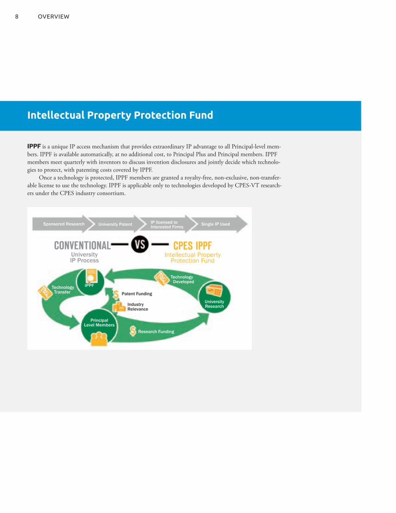
IPPF is a unique IP access mechanism that provides extraordinary IP advantage to all Principal-level mem-bers. IPPF is available automatically, at no additional cost, to Principal Plus and Principal members. IPPF members meet quarterly with inventors to discuss invention disclosures and jointly decide which technolo-gies to protect, with patenting costs covered by IPPF.
Once a technology is protected, IPPF members are granted a royalty-free, non-exclusive, non-transfer-able license to use the technology. IPPF is applicable only to technologies developed by CPES-VT research-ers under the CPES industry consortium.
Intellectual Property Protection Fund
IP licensed to Interested Firms
8 OVERVIEW

The CPES mini-consortium program pro-vides a unique forum for creating synergy among industries and defining new research di-
rections to meet future industry needs. The formation of the mini-consortium allows CPES to pool resources and focus on developing pre-competitive technologies to address common challenges, and sharing the re-search results among mini-consortium members.
Mini-consortium members are enrolled in CPES as Principal Plus Members, with annual contribution
of $50,000. They gain tangible benefits via research collaboration with CPES as a member of one of the mini-consortia on focused research:
• PMC (Power Management Consortium)• HDI (High Density Integration)• REN (Renewable Energy and Nanogrids)Companies interested in more than one focused
research area may join another mini-consortium for an additional annual contribution of $50,000 each.
CPES Mini-Consortium Program
9CPES ANNUAL REPORT 2016

In 1997, at the request of Intel, CPES established a VRM mini-consortium to address the issue of power management for future generations of microprocessors, targeting sub-1 volt and 100-200 amps current. As a result of this focused research, the CPES team has developed a multi-phased voltage regulator module (VRM). Instead of paralleling power semiconductor devices to meet the current demand and efficiency require-ments, the research team proposed to parallel a number of mini-converters. By paralleling the mini-converters and phase-shifting the clock signal, the team was able to both cancel the significant part of the output current ripple and increase the ripple frequency by N time, where N is the number of channels paralleled. This resulted in significant demonstrated improve-ment—specifically:
• 4 times improvement in transient response• 10 times reduction in output filter inductors• 6 times reduction in output capacitors• 6 times improvement in power density, and 3 times im-
provement in profileThe new generation of Intel’s microprocessor is operating
at a much lower voltage and higher current, with a fast dy-namic response in order to implement the sleep/ power mode of operation. This mode of operation is necessary to conserve energy, and to extend the operation time for battery-operated equipment. The challenge for the voltage regulator module in this case is to provide a precisely regulated output with fast ,dynamic response in order to transfer energy as fast as possible to the microprocessor. Today, every Intel processor is powered by such multiphased VRMs developed by CPES.
Power Management Consortium (PMC) is an outgrowth of the early VRM mini-consortium initiated in 1997. The goal is to extend its research scope with a focus on developing pre-competitive technologies in the areas of power management for distributed power system architectures, EMI/EMC, power quality, ac/dc converters, dc/dc converters, POL converters in applications including microprocessors, tablets, notebooks, desktops, servers, data centers, networking products, telecom equipment, solid state lighting, battery chargers and other in-dustrial and consumer electronic applications.
The PMC mini-consortium has accumulated a wealth of knowledge and made significant contributions to the power management industry. Since its inception, the program has been supported by more than 30 major semiconductor and
power supplies companies. PMC currently has 17 members. In the past year three new members joined the PMC, Inven-tronics, Intel, and ON Semiconductor.
The PMC places a significant emphasis on developing high-efficiency, high-power density switch-mode power sup-plies based on recent developments in wide-bandgap power de-vices such as gallium-nitride (GaN) devices and silicon carbide (SiC) devices. This emphasis will be highly leveraged with the recent DOE award of “PowerAmerica.” CPES is a partner in this multi-industry multi-university collaboration program for a period of five years. The CPES role is to work with the wide-bandgap (WBG) manufacturing industry to explore potential applications and impacts of GaN and SiC devices to power conversion technologies.
The proposed GaN-based research will use several test beds to demonstrate the benefit of GaN-based power convert-ers:
(a) High frequency adapter with 26W/in3 power density and above 93% efficiency.
(b) High frequency 1-3kW off-Line distributed power systems with 200-300W/in3 power density and above 96% ef-ficiency.
(c) High frequency 6.6kW bidirectional on-board charger (OBC) for plug-in electric vehicles (PEVs) with 95% efficiency and 30-50% volume reduction.
Work Scope:• High performance VRM/POL converters• High efficiency power architectures for laptops,
desktops and servers• High frequency magnetics characterization and design• High-efficiency and high-power density power supplies
with wide bandgap power devices• Digital control • EMI• Solid state lighting• Power management for PV system• Power management for battery system
PowerManagementConsortium(PMC)
POWER TECHNOLOGY
Power Management Consortium (PMC)
CPES Mini-Consortium ProgramOVERVIEW10

HDI was created in 2011 as a mechanism for CPES and industry members to address emerging or long-term challenges in power-electronic integration.
Over the past two decades, CPES has secured research funding from major industries, such as GE, Rolls-Royce, Boeing, Alstom, ABB, Toyota, Nissan, Raytheon, Groupe Safran and MKS, as well as from government agencies including the NSF, DOE, DARPA, ONR, U.S. Army, and the U.S. Air Force, for research pursuing high-density system design. CPES has developed unique high-temperature packaging technology critical to the future power-electronic industry.
The commercialization of wide-bandgap semiconductors as Silicon Carbide (SiC) and Gallium Nitride (GaN) has shifted switching fre-quency beyond tens of megahertz, power rating beyond megawatts, and junction temperature beyond 250°C. The switches’ ancillaries, characterization metrology, modeling method, packaging process, and manufacturing paradigm need to be transformed.
In the past, HDI has developed die-attach materials that can be processed at low temperatures, yet are reliable at the temperature of the wide-bandgap junction. Processes have been developed to encapsulate ultra-thin planar packages with polymer having high glass transition temperature and dielectric strength. Techniques to decouple the noise loops have been identified to enable high dv/dt commutation. Magnetic powder with low core loss density has been synthesized from magnetic metals for 1-5 MHz operation. Inductors have been integrated into the converter package as a substrate to achieve power density approach-ing 1kW/in3. Design methodologies for high-temperature capacitors, power buses, protection, sensing, digital control, etc., have also been documented.
HDI has been experimenting with new breeds of gate drivers, sensors, active and passive filters, magnetic materials and components, encapsulants, substrates, and additive manufacturing. A wide range of products, from power adapters to power-electronic building blocks, are expected to see significant improvement in power density, efficiency, and signal integrity, thanks to the adoption of the technological advances.
HDI tasks are scoped to advance Wide-Bandgap Systems, Mag-netic Components, and Module Integration.
This current scope of work includes the following topics:
Wide-Bandgap Systems ‐ • Active dv/dt Control of 600 V GaN Switches• Characterization of Multi-kV SiC MOSFETs• High-Density 65 W Laptop Adaptor• Integrated Multi-Phase Inductor for Voltage Regulator
for Small Portables• PCB-Integrated Magnetics for High-Efficiency, High-
Density Front-End Power Supply
• Components• Characterization and modeling of wide-bandgap semi-
conductor devices (SiC and GaN)• Low‐profile magnetic substrate• Magnetic structures with high energy density
• Magnetic Components• Additive Manufacturing of Magnetic Components• Integrated Design of Power Transfer and Fringing Attenu-
ation for Weakly Coupled Coils• Integrated Multi-Phase Inductor for Voltage Regulator
for Small Portables• PCB-Integrated Magnetics for High-Efficiency, High-
Density Front-End Power Supply• Characterization of High-Power Inductors
• Module Integration• Reliability Measurement of Metal-Ceramic Substrates
with Sintered Silver Joint• Current Sensor Integrated with SiC MOSFET Module• High-Efficiency, Diode-Less 1.2 kV SiC MOSFET Half-
Bridge Module
Mini-Consortium on High Density Integration (HDI)
HighDensityIntegration(HDI)Work Scope:
• Wide-band gap devices• Material and component
characterization• Active module integration• High frequency magnetic
integration• Converter integration• Wide power range (10 W - 100 kW)• High frequency (100 kHz - 10 MHz)• High temperature (≥ 250 ºC)
Research Center
SiC Module 45W Adapter
1kWFront-endConverterMobileVRM
11CPES ANNUAL REPORT 2016

Mini-Consortium on Renewable Energy and Nanogrids (REN)This CPES mini-consortium program provides a unique forum for creating synergy among industries and defining new research directions to meet future industry needs. The REN mini-consortium allows CPES to pool resources and focus on developing pre-competitive technologies to address common challenges, and sharing the research results among mini-consortium members. The main objective of the REN mini-consortium is to expand CPES’ expertise in autonomous electric power systems (already established for transportation and IT), into the area of renewable energy and storage systems integration in the electric grid through power electronic con-verters, while providing competitive research and education in that area.
The current research directions of the REN mini-con-sortium comprise three different topics listed below with corresponding sub-topics. Additionally a REN system testbed structure is planned to be designed and built in the near future for experimental validation purposes.
The current scope of work includes the following topics:
• High-Power WBG-Based Power Converters‐ • Evaluation and design of Si based and SiC
impact on modular multilevel converters for MV drives
• High frequency control of modular multilevel converters in ac-dc and dc-dc mode
• Design of SiC based modular multilevel convert-ers with 1.7Kv, 3.3 kV 10kV devices (package, gat-drive, PEBB, converter, system)
• WBG-Based Power Electronics Technology• Characterization of MV SiC devices• Design and evaluation of SiC-based SST• Design of high-efficiency SiC-based ECC-G2,
single-phase to LVDC• Static and dynamic nonlinear droop control for
LVDC distribution systems
• Renewable Energy integration• Design of Si-based multilevel ECC for grid-tied
applications (ac-dc + dc-dc)• Impact of PV inverters at distribution and trans-
mission level
• Stability and Dynamic Interactions in Power Converter Systems• VSM modeling and converter control design for
grid-tied inverters• VSM modeling and converter control for
STATCOM• Stability assessment and investigation of AC
and DC systems• SiC-based IMU design• Evaluation of dynamic interactions between mul-
tiple STATCOM units
CPES Mini-Consortium ProgramOVERVIEW12

In its effort to develop power processing systems to take electricity to the next step, CPES has cultivated research expertise encompassing five technology areas: (1) power conversion technologies and architectures; (2) power electronics
components; (3) modeling and control; (4) EMI and power quality; and (5) high density integration.
These technology areas target applications that include: (1) Power management for information and communications technology; (2) Point-of-load conversion for power supplies; (3) Vehicular power converter systems; and (4) High-power conver-sion systems.
In 2016, CPES sponsored research totaled approximately $2.1 million. The fol-lowing abstracts provide a quick insight to the current research efforts.
RESEARCH
Application Areas
Technology Areas
Power Management for Computers, Telecommunications & Others
Power Conversion Topologies & Architectures
Point-of-Load Conversion
Power Electronics Components
Vehicle Power Converter Systems
Modeling and Control
High-Power Conversion Systems
EMI and Power Quality
High Density Integration
13CPES ANNUAL REPORT 2016

RESEARCH
Multi-Phase Auto-Tuning Self Compensating Power Supply Control Systems Sponsored by: Energy Research Corporation (September 1, 2012 – August 31, 2015)
The multi-phase voltage regulator (VR) has been widely used to power microproces-sors. For multi-phase VR, a constant output impedance design is usually used to reduce the output capacitor bank. Conventionally, a fixed analog compensation network is chosen to compensate the worst-case component (such as inductor and output capacitor) variations on the plant, which will limit the converter bandwidth. Furthermore, since a micropro-cessor runs into sleep mode very frequently, several green-mode functions have been used to improve the light load efficiency such as phase shedding, discontinuous mode opera-tion, and frequency changes. However, the plant characteristic will also change with these techniques under sleep mode, and will influence the stability and transient response during mode transitions. Therefore, it is very challenging and attractive to investigate multi-phase self-tuning power supply control systems which can compensate the component variation and mode transition without suffer-ing from the worst-case design compromises. In this project, a self-tuning power supply control system is developed to self-identify the plant characteristic change from component variation and operating mode transitions, and then adaptively adjust the compensation parameters to maintain stability and system performance. Therefore, external compensa-tion circuitry and the output capacitor bank can be reduced to reduce total cost. We have already proposed several control methods with auto-tuning function to improve transient performance of voltage regulator, including self-compensated DCR current sensing, adap-tive PLL loop for variable frequency control, and high bandwidth DDR VR with adap-tive zero positioning. The proposed control concepts have been validated with Intel CPU emulator (Gen4 VTT tool).
Sponsored ResearchHigh Density High Efficiency AdapterSponsored by: Department of Energy thru PowerAmerica Institute (February 1, 2015 – March 31, 2016)
The adapter is highly driven by efficiency and power density for all forms of portable electronics. The adapter below 65W power level is chosen for the demonstration for its potential economic impact, with wide range applications covering a large section of mobile devices, including tablet, notebook, and many other portable electronics equipment. Today, most of the adapters are only operating at rela-tive low frequency (<100 kHz) with the state-of-the-art efficiency up to 91.5%. However, the low frequency operation limits the adapter power density at 6-11W/in3.
High efficiency and high frequency are the catalysts for size reduction. The emerging GaN device, with much improved figures of merit, opens the door for an operating fre-quency well into the MHz range. To realize the full benefits of GaN, a number of issues have to be addressed carefully, including soft-switching topology selection, high-frequency magnetics, control, packaging, gate drives and thermal management. During Year 1 of this program, we have successfully demon-strated that the GaN-based adapter design is capable of operating at 1-2 MHz frequencies with an improved efficiency up to 93.5%. Subsequently, a power density of 27W/in3, which is a three-fold improvement over the state-of-the-art product, was successfully dem-onstrated at 45W and 65W levels. In this MHz adapter design, we have implemented a number of unique features:• A flyback with active clamp circuit is
applied to recycle the transformer leakage energy and, thus, realize soft-switching for the primary switches, which brings over 90% reduction of switching losses. This enables the circuit to operate at 1-2 MHz while achiev-ing high efficiency. The noise associated
with high di/dt and dv/dt are also sig-nificantly reduced.
• 6-layer PCB board based high-frequen-cy transformer design to enable high power density.
• Common-mode noise is significantly reduced using the patented transformer shielding technique. The shielding pro-vides more than 20 dB common-mode EMI reduction across the full frequency range (150 kHz~30MHz), thus reduc-ing the EMI filter to a single-stage filter.
• With the exception of the EMI filter and bulk energy storage capacitor, ev-erything can be fully automated in the manufacturing process.
High Frequency GaN Converters for Distributed Power SystemsSponsored by: Department of Energy thru PowerAmerica Institute (February 1, 2015 – March 31, 2016
The ever increasing demand for high-efficiency and high-density switch-mode AC/DC power supplies includes but is not limited to computers, telecommunication, data centers, electrical vehicle battery char-gers, PV inverters, numerous industrials, and aerospace applications. Collectively, these products consume more than 10% of the total electric power. In the proposed effort, we will use high voltage GaN devices for the
1MHz 65W active clamp flyback converter for AC-DC adapter application
14

server power supplies to push its frequency 20 folds, from today’s 50-100 kHz to 1-5 MHz. As a result, the power density of front-end converter can be dramatically increased from today’s 30-50 W/in3 to 100-150 W/in3. Furthermore, it is envisioned that the front-end power processing to be fully modularized. In this manner, a customized power system can be synthesized by using simple modular building blocks such as multi-phase power factor correction (PFCs), and high voltage DC/DC converters and DC/DC transform-ers (DCXs) for input/output isolation. These front-end converters are followed with already standardized multi-phase distributed Point-of-Load (POL) converters. In the Year 1 of this program, we have successfully devel-oped a 1kW, 1-3MHz critical mode PFC with 99% peak efficiency and more than 200W/in3 power density. A PCB integrated coupled-inductor has also been proposed for this PFC circuit to further improve its power density and achieve balance control on the circuit parameters to greatly reduce common mode EMI noise. For the DC/DC stage, we have developed a 1kW, 1MHz 400V/12V DCX with PCB winding based matrix trans-former. It achieves 97% peak efficiency and 700W/in3 power density.
This high density DCX will be further improved to meet the specifications. pro-posed by iNEMI for future DC datacenter with onboard 380V/12V module. (Recently, the International Electronics Manufactur-ing Initiative (iNEMI) at the behest of IBM and other server manufacturers undertook a project to develop an industry standard for DC-DC converters. This converter is used to step down 380V directly to 12V and is placed directly on the motherboard). Compare to today’s AC datacenter, the DC datacenter with onboard 380V/12V module will bring at least 7% improvement in system efficiency.
High Efficiency High Density GaN Based 6.6kW Bi-Directional On-board Charger for Plug-in Electric Vehicles (PEVs)Sponsored by: Department of Energy Sub-Awardee of: Delta Products Corporation (October 1, 2014 –September 30, 2017)
This project involves the development and commercialization of a lightweight, compact and efficient bidirectional on-board charger (OBC) for plug-in electric vehicles (PEVs). PEV hereafter refers to plug-in hybrid electric vehicles (PHEV) and battery electric vehicles (BEV).
The OBC uses novel circuit architectures and control schemes enabled by Gallium Nitride (GaN) based wide- bandgap (WBG) semiconductors to obtain charger efficiency better than 95% and reduce volume and mass by approximately 30% to 50% of the existing state-of-the-art silicon (Si) based chargers by pushing converter switching frequency to the MHz range. A Si-based bidirectional OBC is typically implemented with two separate modules: a charger and an inverter. A GaN-based bidirectional OBC can integrate both functions in a single module. It will result in substantial reductions in size, weight and cost.
With Chrysler’s commitment, this project aimes to demonstrate the viability and commercial potential for WBG semiconduc-tors in PEV applications. The core charger/inverter technology will also provide the added consumer benefits of providing emer-gency or convenience ac power on a vehicle, a feature that is strongly desired by consumers. In addition, it supports effective vehicle-to-grid (V2G) integration. V2G enables more efficient energy management practices, such as wind and solar photovoltaic distributed gener-ation, peak shaving, and discounted off-hour charging rates for customers. All of which will help support the mainstream commercializa-tion of PEVs. This project brings together four world-class organizations including: the
Center for Power Electronics Systems (CPES); Transphorm, Inc.; Delta Products Corpora-tion; and Chrysler LLC.
In this project, CPES will focus on developing advanced circuit architectures and control schemes for GaN based battery charger. The main tasks included high-fre-quency GaN device and driver evaluation; topology selection and evaluation; high-fre-quency magnetic components development; reference design of high frequency PFC stage, dc/dc stage and EMC filters.
Research of High-Efficiency High Density Power Conversion ArchitectureSponsored by: Huawei Technologies Co., Ltd. (August 19, 2015 – February 19, 2017)
This project will develop a high fre-quency (>MHz) 48V/1V power module with an efficiency target of 91%. A PCB winding based high frequency transformer structure will be used to help increasing power density as high as 400W/in3. A detailed analysis about the trade-off between system efficiency and power density will also be completed.
A 6.6kW 500kHz Level 2 on board battery charger is built using a novel variable DC-link voltage structure.
15CPES ANNUAL REPORT 2016

RESEARCH
SiC Module EMI Control by Transient Shaping and Shielding TechniqueSponsored by: Toyota Motor Engineering Manufacturing NA, Inc. (August 15, 2014 – March 31, 2015)
The transition edges of PWM gate current and gate-source voltage will be syn-thesized from such basis functions as linear, exponential, and sinusoidal. The resultant gate-drive waveforms will excite silicon and silicon-carbide modules in a bidirectional boost converter over specified voltage and power ranges. Selected transition shapes will be synthesized using commercial parts for experimental verification. The project will document the tradeoffs among transition shapes, switch materials, interconnects, loss, and noise, along with recommendations for preferred practices.
Control of Modules of Parallel SiC Switching CellsSponsored by: Toyota Motor Engineering Manufacturing NA, Inc. (August 15, 2014 – March 31, 2016)
The objective of the project is to develop a gate driver/controller that would commutate a large number of paralleled SiC MOSFETs reliably, as well as balance the performance of the dies with respect to power or thermal distributions. Development of guiding prin-ciples for the design and fabrication of a power module of such paralleled MOSFETs will also be achieved.
Constant-Flux Magnetics for Power ConversionSponsored by: National Science Foundation (November 15, 2012 – April 30, 2016)
At least 30% of the volume in commer-cial inductors store no or negligible energy. The “constant-flux” concept improves energy density by filling the available volume with as much magnetic (core) materials as practi-cally feasible, then dispersing the windings to shape the distribution of magnetic flux, e.g., to distribute magnetic flux uniformly. In this project, guiding principles will be developed from the structural and field standpoints to realize the constant-flux concept. Performance metrics, such as inductances, capacitances, and quality factor will be modeled, quanti-fied, and compared with the corresponding benchmarks.
Tunable Energy Efficient Electronics (TE3)Sponsored by: DARPA (December 1, 2015 – November 30, 2018)
In modern defense systems, processing of electrical power to suitable voltage level and frequency is a key factor in achieving high performance, light weight, improved reliabil-ity and high efficiency. A majority of defense applications often require power processors to operate with fluctuating source, load or envi-ronment. Passive components with added-tunability are sought to provide adaptability to different circuit conditions. They will add a major leap in size optimization, control-lability and circuit design strategies. This project is going to design and make tunable power inductors, transformers, capacitors and current sensors to reduce weight of power passives and increase power handling capacity. TE3-based dc-dc power converter system will be designed for achieving high power density and efficiency with adaptability to fluctuations in source, load and environment.
Power Integration by Multifunctional MoldingSponsored by: National Science Foundation (August 1, 2015 – July 31, 2017)
Power Modules are employed in elec-tronic systems to lower part count, improve reliability, and reduce cost. The type of power module addressed herein comprises a com-plete dc-dc switched-mode converter in one package. Power switches, gate drivers, sensors, controllers, lead frames, and filter inductor are integrated into one building block that is encapsulated in molding compound. A 50W module with efficiency exceeding 90% would fit into a volume of 1.5 x 1.8 x 0.6 cm3.
While the filter inductor is known to be undesirably bulky, the unused space filled up by the molding compound might actually be larger than the inductor’s volume. Power density would be improved significantly if the molding compound also stores energy so that, with appropriately designed winding, the module case also functions as the inductor. Such power integration by multifunctional molding has not been demonstrated so far because of two reasons. First, magnetic mate-rials are usually kept away from a switching loop for fear that the increased in stray mag-netic field would adversely affect converter’s operation. Second, an encapsulant with sig-nificant relative permeability (20–30) is dif-ficult to synthesize using low temperature and low or no pressure.
The objective of the research is to inte-grate the energy-storage function into the encapsulating case of the power module, thereby reducing material usage and possibly simplifying manufacturing process. Funda-mental contributions are anticipated in mate-rials and electrical engineering, education, and application. Encapsulation material that integrates mechanical/chemical (protective) and electrical (energy storage) functions are to be synthesized using low temperature and low pressure. Multi-magnetics module (MMM) with unexplored electromagnetic properties Double-pulse tester for current balancing
Sponsored Research16

and design methodology are to be devised to take advantage of such material. Oper-ability of power-electronic converters are to be assessed the presence of magnetic media. Converter topologies are to be synthesized to leverage the field couplings inside an MMM. All fundamental advances are to culminate in a manufacturing process of multi-magnetics module with less materials and cost, possibly.
MHz GaN Converter with IsolationSponsored by: Texas Instruments
This project starts with the design of the converter for zero-voltage switching over the full range of input voltage and output power to establish component requirements. Magnetic design of leakage inductance and harmonic losses in the coupled inductors with different winding structures are analyzed by finite-element simulation. The design of gate drive, loss analysis, effect of layout impedance, and other issues are addressed, leading to hardware verification with efficiency exceed-ing 85% at 5MHz and 30W output.
High-Density Integrated InductorSponsored by: Texas Instruments
The “constant-flux” concept proposed recently is leveraged to distribute magnetic flux to improve energy density, lowering the profile of an inductor. The optimal flux distri-bution is identified mathematically, and veri-fied by simulation. It is then applied to reduce
the dc resistance of a commercial inductor by a factor of two, keeping the outer dimensions and inductance the same. Thermal-limited current rating is improved by 50%, whereas saturation- limited current rating is improved by 20% thanks to the suppression of flux crowding.
Point-of-Load Inductor with Two-Dimensional GappingSponsored by: Texas Instruments
Point-of-load converter at light load has low efficiency owing to the “fixed losses” such as core loss and ac winding loss. Two-dimen-sional (2D) gapping is applied for a ferrite core to shape inductance versus load current to reduce inductor loss at light load. Since the maximum inductance of conventional stepped gap is limited by the cross-sectional area of the thin gap, a 2D gap is formed by joining two orthogonal gaps to gain flexibility. Higher inductance is achieved at light load compared with uniform-gap and stepped-gap geometries having the same volume and dc
resistance. AC resistance is reduced at light load thanks to a magnetic path that steers ac flux away from the winding. Two C-cores with 2D gap were fabricated and tested on a buck converter with 50% reduced total inductor loss at 10% load current.
Optimization of ac/ac Motor Controller Power Quality and EMI Filter Topology Sponsored by: United Technologies Aerospace Systems (January 1, 2012—December 31, 2015)
The objective of this work has been the development and optimization of modular power converters for aerospace applications. This has included the development of new power conversion topologies; the design of high-efficiency, high power density topologies based on wide-bandgap power semiconduc-tors; the combined design of power quality and EMI filters; as well as the effect of the thermal and electrical characteristics associ-ated with these new materials and semicon-ductors. Extensive modeling and optimization work has been conducted too as part of this effort. The focus of the first year was spe-cifically aimed at the design and evaluation of three-phase ac-to-ac power conversion topolo-gies from an EMI filter standpoint, seeking the best solution for motor drive applications.
The second phase of this work honed its efforts on the optimization of small local converters, each built on PCB cards address-ing the combined power quality, EMI and thermal requirements and fed by variable frequency ac or higher voltage dc power bus and output power circuits that provide regu-lated 28 V dc power. The effect of the thermal and electrical characteristics associated with a number of power topologies and the trade off in their performance in terms of weight, size and perceived reliability was investigated. Addressing single-phase power conversion first, a novel three-level semi-bridgeless PFC topology was developed to achieve 99% effi-ciency. For three-phase power conversion, a dual channel Vienna-type three-level con-verter was developed and tested surpassing 99% efficiency too.
The third phase of this project, also tar-geting PCB-based power converters, addressed the efficient power conversion from 270 V DC to 28 V DC, for which a multi-kilowatt
Prototype of a 1.2 kW three-phase isolated AC/DC converter with 97% efficiency and 22W/in3 power density.
Double pulse tester for DrGaN
17CPES ANNUAL REPORT 2016

RESEARCH
resonant converter with isolation was designed and developed achieving 98% efficiency. The focus in this case was on the transformer design, high current operation (>100A), and EMI filter design to meet input and output requirements.
The fourth phase of this project, com-pleted in 2015, consolidated the work of the previous two years and merged the ac-dc and dc-dc power conversion stages to design a three-phase 115V ac to 28V dc isolated power converter of maximum power density and maximum efficiency for a given form factor, which has required the reformulation of the design optimization procedure used to explore the potential of PCB-based power conversion systems. A significant effort was spent in the optimization procedure itself that conversely, with existent design approaches, sought to maximize the power processing capability of the converter in question while keeping as hard limits the size and volume of the unit, pursuing to a target efficiency of 98 %.
In what is a new phase just started in 2016, a similar approach will be used to develop a modular card-based dc-ac inverter system capable of feeding and driving motor loads. A key addition to the problem has been the incorporation of an onboard digital con-troller to the converter card system.
Terminal Modeling of Noise Source in Switching Power ConvertersSponsored by: Hispano Suiza, SAFRAN (October 1, 2010—September 30, 2016)
The main objective of this research over the past years has been on the development of terminal models of noise sources in switching converters for simplified EMI analysis, models which must be scalable for different load and source conditions. Conventional methods of EMI modeling on the other hand use physics based models of semi-conductor devices and EMI coupling paths. Due to the complex nature of these models the simulations often fail to converge or lead to unusable results.
In its last two phases, this project has
explored the use of terminal models for the development of EMI filter design procedure. Its main focus was the design of filters for par-allel inverters using interleaved PWM tech-niques. Research efforts aimed at simplifying the simulations by using Thevenin or Norton models of these noise cells. Here “noise-cell” may refer to both device level (single device or a Phase-leg) and converter level abstraction. This method has been successfully demon-strated so far on an industrial low-voltage 10kW motor drive, for which the unter-minated EMI model of its 3-phase voltage source inverter (VSI) was built showing how it could predict the EMI behavior of the motor drive under varying conditions. In 2014, the method developed was extended to enable the modeling and prediction of EMI noise gener-ated by converters operating at higher switch-ing frequency (50–100 kHz) enabled by the use of SiC devices. This required the complete reformulation of the measuring techniques and modeling methodology employed, ren-dering the approach capable of predicting common-mode (CM) up to 30 MHz; a feat which had not been achieved before. In its new phase, planned from 2015–2016, this project will make use of the EMI modeling and filter design procedures developed in the past year to support the design of integrated power supplies for gate-drive and avionics applications operating in harsh environment in terms of dv/dt transients and also high temperature. Specifically, the gate-drive power supply will be used to power an active gate-driver circuit with dv/dt and di/dt control to be developed for 600V GaN semiconductors, while the avionic power supply will addition-ally have to withstand high input voltage variability (10–100%). The project will also conduct a system study to determine the tradeoffs between switching frequency, dv/dt rate, inverter efficiency, EMI filter, and harness and motor size.
After a year of execution, the project has successfully demonstrated the active gate-drive control method for GaN power devices, as well
as the integration of gate-drive and general purpose power supplies with reinforced-isola-tion, PCB embedded transformers, and active stage switching at 1 MHz thanks to the use of GaN power semiconductors.
Strategies for Wide-Bandgap, Inexpensive Transistors for Controlling High Efficiency Systems (Switches)Sponsored by: ARPA-E, ADEPT Program (Advanced Research Projects Agency Energy, Agile Delivery of Electrical Power Technology) Sub–Awardee of: HRL (March 6, 2014—March 7, 2017)
With the sponsorship of ARPA-E, CPES has partnered with HRL Laboratories to demonstrate ultra-high efficiency, low-cost power modules for future 1.2kV, 100A, ver-tical Gallium-Nitride (GaN) devices under development at HRL. These devices, expect-edly capable of commutation speeds in the 100–200 V/ns range, will minimize switching losses to the extent were system efficiencies of >99 % are expected at the power converter level. To this end, CPES will build a 30kW, 800V dc, three-phase boost rectifier demon-strator. In its first year, CPES has developed several ultra-low parasitic inductance package concepts using ribbon topside interconnec-tions for the GaN devices and Flex PCB for the gate-terminals, with which it has reduced this parasitic component to less than 5 nH. Similarly, the module design has targeted the minimization of the parasitic capacitances to ground as an EMI containment strat-egy. A first prototype of the power module using 1.2kV, 90A, SiC MOSFET devices was recently built to validate the module design. An advanced module concept utilizing ribbon bonding for the power terminals and a flex-PCB for the gate-loop of the power module attained ultra minimized parasitic compo-nents. These power modules will now be built to demonstrate in the last year of execution of the project the 30 kW boost rectifier.
Sponsored Research18

Thermal-Electrical-Mechanical Modeling of IGBT Module Failure ModesSponsored by: Huazhong University of Science and Technology (August 8, 2014 – July 31, 2017)
Insulated Gate Bipolar Transistors (IGBT) are one of the major players in modern power conversion, especially for medium and high power applications. The reliability of these devices remains to be a major concern, topic which Huazhong University of Science and Technology (HUST) has been studying jointly with Techsem Semiconductor Co., and now is interested in pursuing jointly with CPES. The primary goal of this research will be to investigate the possible failure modes of commercial IGBTs, including:
1) module layout and its influence on the electric field and thermal distribution; 2) wire bond structure and its impacts on the internal current distribution; 3) Direct Bond Copper (DBC) substrate preparation and its reliability; 4) thermal interface mate-rial (TIM) selection and its influence on the module reliability; 5) encapsulation of high voltage IGBT modules.
Optimal Magnetic Component Design for Boost ConvertersSponsored by: General Motors (September 5, 2014 – March 31, 2015)
The push towards higher power, while simultaneously targeting higher power density in drive systems for traction applications, has resulted in the need to rise the dc-bus voltage of the converter system, to increase efficiency as well as to provide the needed design flexibility for the traction inverter and electrical motor. This is enabled by the use of a boost dc-dc converter to interface the battery pack and the inverter, which regu-lates the dc bus voltage under varying battery voltage and state of charge (SOC). The boost ratio required ranges from 2:1 to 4:1, for power levels ranging from 60–100 kW. The
electrothermal stress on the boost inductor of this converter is hence significant, which has become a key barrier in the accomplishment of the system power density goals. CPES has accordingly initiated a focused effort to explore alternative dc-dc boost converter and boost inductor topologies, ultimately pursu-ing the formulation of new design criteria that can minimize the inductor weight. To this end, the research conducted focused on the development of new electrothermal models for the inductors, pursuing the use of closed-form analytical equations instead of the time-consuming finite-element method conventionally used. Optimization proce-dures developed in CADES, an optimization software suite, were successfully used for this purpose.
SiC-PEBB Modules for Next Gen-eration MVDC Integrated Power Systems—Development of the SiC-Based PEBB 1000Sponsored by: Office of Naval Research (August 1, 2014 – July 31, 2016)
This project will develop 1kV Silicon-Carbide (SiC) based power electronics build-ing block (PEBB) modules, named PEBB 1000. These SiC-PEBBs will truly enable, for the first time, the notion of a high power density PEBB-only integrated power system for future Navy ships, profiting doubly from the system and commercial advantages fea-tured by the PEBB modular concept, and from the power processing advantages offered
by SiC semiconductors. As such, power density, efficiency, high control bandwidth, modularity, voltage and current scalability, reconfiguration flexibility, simplicity, and the potential for low-cost commercial off-the-shelf technology become a factual reality. For demonstration and evaluation purposes, multiple PEBB 1000 units will be developed by CPES to evaluate the performance of the PEBB in ac-dc, dc-ac and dc-dc applications. This will allow for a comprehensive assessment of the PEBBs, converters, and their system-level impact. The project is also evaluating alternative SiC devices, and will target the use of 1.7 kV, 300 A, SiC MOSFET power modules from CREE, as well as 1.5 kV 200 A, SiC MOSFET power modules from GE. In a parallel effort funded by ONR, GE Global Research will develop the PEBB 6000 unit using 10kV SiC MOSFET power modules from Powerex, using CREE devices, which will enable the comprehensive evaluation of the SiC-PEBB integrated power systems for future Navy ships. The first PEBB 1000 prototype will be fully tested in March 2016, and converter level tests are expected to follow soon thereafter.
High Power Solid State CircuitsSponsored by: Office of Naval Research Sub–Awardee of: ABB (May 1, 2015 – October 31, 2016)
The main goal of the team at CPES, Vir-ginia Tech, has been to develop a power con-verter concept with current limiting capability that can effectively withhold its stored energy during fault conditions. The converter has a modular structure being capable of scaling up its operation in both voltage and current by the series and parallel connection of its modules. At the system level, the main goal will be to demonstrate the current-limiting capability of the converter both under fault and overload conditions, demonstrating as well potential to expand the safe operating area of the system by sharing the limited load current among multiple power converters.
Three-phase inverter system used for validating EMI models.
19CPES ANNUAL REPORT 2016

RESEARCH
Lastly, coordination aspects among power converters with current-limiting function and solid state circuit breakers will be investigated in order to formulate the system level circuit protection scheme.
To this end, CPES has been devoted to the design, modeling and simulation of power converters rated at 1 kV DC. System level simulations were conducted to evaluate the current-limiting functionality both during faults and overload conditions. These simula-tions were run within the same power system environments used to test the solid state circuit breaker. Accordingly, joint simulations will be run to investigate the coordination requirements among the power converters and solid state circuit breakers.
The last 9 months of execution of the project have been devoted to the construc-tion of a 45 kW three-phase modular con-verter demonstrator based on the PEBB 1000 units developed at CPES using 1.7 kV SiC MOSFET power devices. This converter pro-totype will be used to demonstrate the fault handling capabilities of the converter when controlled under the proposed methods devel-oped.
Developing the Future of Wide Bandgap Power Electronics Engi-neering WorkforceSponsored by: Department of Energy (January 1, 2015 – July 31, 2021)
The goals of the proposed project are first to train the next generation of U.S. citizen power engineers with WBG power semicon-ductor expertise, thus aiding in fulfilling the future workforce needs in this field. Second,
to broaden the range of WBG-based power electronics by conducting research and devel-opment on high-efficiency grid apparatus and high-efficiency electrical power systems. And third, to enhance the power engineering cur-riculum by formalizing WBG-oriented design procedures for power electronics components and systems that can effectively integrate the inherent, challenging material characteristics of these devices, which have effectively ren-dered design procedures for Silicon (Si) based power electronics obsolete.
This project expects to graduate 10 MS students during its 5 years of execution, fund the first two years of 10 PhD students, and fund the first year of 5 additional MS and PhD students. In this period of time, 3–5 PhD students will expectedly graduate from Virginia Tech having passed through the proposed traineeship, and 5–10 more will do so in the following years. In all, a total of 45 graduate student assistantships will expect-edly have been granted throughout the five years of the WBGen program. This will not only have an immense impact on the success of the WBGs research programs at Virginia Tech, but will consequently spring immeasur-ably positive effect on the power engineering workforce over the next 5 to 10 years. Fur-thermore, the DOE and DOD laboratory and industrial partnership established in the traineeship will also benefit significantly from the interaction with the participating graduate students, cementing what are already strong relationships between the partners and CPES, and CPE, into a solid network of power engi-neering training, research and development.
Gate driver, Rogowski current sensor board and signal processing board for 1.7 kV SiC MOSFETs used for PEBB 1000 project.
Sponsored Research20

New Projects approved and starting in the coming months:
Highly Integrated Wide Bandgap Power Module for the Next Generation Plug-In VehiclesSponsored by: Department of Energy Sub – Awardee of: General Motors
Efficient and Reliable Power Takeoff for Ocean Wave Energy HarvestingSponsored by: Department of Energy
Next Generation Electric Machines: Megawatt Class MotorsSponsored by: Department of Energy Sub – Awardee of: General Electric
21CPES ANNUAL REPORT 2016

12-010Algorithm and Implementation Sys-tem for Measuring Impedance in the D-Q DomainBy Gerald Francis, Rolando Burgos, Du-shan Boroyevich, Fred Wang, Zhiyu Shen, Paolo Mattavelli, Kamiar Karimi, Sheau-Wei Johnny FuU.S. PATENT: 9,140,731Issued: September 22, 2015
12-009Method of Evaluating and Ensuring Stability of AC/DC Power SystemsBy Rolando Burgos, Dushan Boroyevich, Fred Wang, Kamiar KarimiU.S. PATENT: 9,136,773Issued: September 15, 2015
11-075Two-Stage Bi-Directional Single-Phase Converter with DC-Link Capaci-tor ReductionBy Dong Dong, Dushan Boroyevich, Ruxi Wang, Fred WangU.S. PATENT: 9,071,141Issued: June 30, 2015
INTELLECTUAL PROPERTY
U.S. Patents Awarded11-113DC-Side Leakage Current Reduction for Single-Phase Full-bridge Power Converter/InverterBy Dong Dong, Fang Luo, Dushan Boroyevich, Paolo MattavelliU.S. PATENT: 9,048,756Issued: June 2, 2015
13-046Multi-Channel Two-Stage Control-lable Constant Current Source and Illumination SourceBy Weiyi Feng, Fred C. LeeU.S. PATENT: 9,000,673Issued: April 7, 2015
13-025Anti-Islanding Protection in Three-Phase Converters Using Grid Synchro-nization Small-Signal StabilityBy Dong Dong, Dushan Boroyevich, Paolo Mattavelli, Bo WenU.S. PATENT: 8,957,666Issued: February 17, 2015
INTELLECTUAL PROPERTY22

15-05312/1/2014Optimal Battery Current Waveform for Bidirectional PHEV Battery ChargerLingxiao Xue, Paolo Mattavelli, Dushan Boroyevich[Patent application sponsored by IPPF]
15-04911/12/2014Coupled Inductor for Interleaved Multiphase Three-Level DC-DC Converters and Its Integrated DesignsMingkai Mu, Sizhao Lu, Yang Jiao, Fred C. Lee[Patent application sponsored by IPPF]
14-1445/27/2014Low Profile Coupled Inductor Substrate with Transient Speed ImprovementYipeng Su, Dongbin Hou, Fred C. Lee, Qiang Li[Patent application sponsored by IPPF; CIP to 13-169]
14-1013/4/2014Transient Performance Improvement for Constant On Time ControlSyed Bari, Fred C. Lee, Qiang Li, Pei-Hsin Liu[Patent application sponsored by IPPF]
14-0972/24/20142-Stage LED Driver with Multi-Channel Constant Current CLL Resonant Converter Xuebing Chen, Daocheng Huang, Qiang Li, Fred C. Lee [Patent application sponsored by Panasonic]
14-0751/6/2014Magnetic Geometry with Programmed Field DistributionKhai Ngo, Han Cui[Patent application sponsored by IPPF]
16-0621/28/2016Low Frequency Common Mode Voltage Control for Systems Interconnected with Power ConvertersFang Chen, Rolando Burgos, Dushan Boroyevich[Patent application sponsored by IPPF]
16-05712/11/2015Omni-Directional Wireless Power Transfer SystemJunjie Feng, Qiang Li, Fred C. Lee[Patent application sponsored by IPPF]
16-04711/19/2015Parasitic Inductances Coupling to Reduce Transient Current Unbalance in Semiconductor Power SwitchesYincan Mao, Zichen Miao, Khai Ngo, Chi-Ming Wang (TEMA) [Patent application sponsored by TEMA]
16-0229/15/2015A Nonlinear Droop Method to Improve Voltage Regulation and Load Sharing in DC SystemsFang Chen, Rolando Burgos, Dushan Boroyevich[Patent application sponsored by IPPF]
16-0088/6/2015Method and Apparatus for Driving a Power DeviceJongwon Shin, Khai D.T. Ngo[Patent application sponsored by TEMA]
16-0077/27/2015A Method of Capacitor Voltage Ripple Reduction for Modular Multilevel Converter Yadong Lyu, Fred C. Lee, Qiang Li[Patent application sponsored by IPPF]
16-0057/13/2015Drivers with Equalizers for Paralleled SwitchesKhai D.T. Ngo, Lujie Zhang, Zichen Miao[Patent application sponsored by IPPF]
15-071 (includes 15-070)1/27/2015Multi-Step Simplified Optimal Trajectory Control Based on Only Vo and Iload
Chao Fei, Fred C, Lee, Weiyi Feng, Qiang Li [Patent application sponsored by IPPF]
15-0692/2/2015Universal System Structure for Low Power AdaptersFred C. Lee, Xiucheng Huang, Qiang Li[Patent application sponsored by IPPF]
15-0682/2/2015A Novel Driving Scheme for Synchronous Rectifier in CRM Flyback ConvertersXiucheng Huang, Fred C. Lee, Qiang Li[Patent application sponsored by IPPF]
15-0671/26/2015New Current Mode Control Based on Charge Control ConceptSyed Bari, Fred C. Lee, Qiang Li[Patent application sponsored by IPPF]
15-0641/21/2015Improved Current-Mode Control with Single-Step Load TransientVirginia Li, Pei-Hsin Liu, Qiang Li, Fred C. Lee[Patent application sponsored by IPPF]
Patents Pending
23CPES ANNUAL REPORT 2016

14-06611/18/2013Hybrid Interleaving Structure with adaptive PLL Loop for Constant On-Time Switching ConverterPei-Hsin Liu, Fred C. Lee, Qiang Li[Patent application sponsored by IPPF]
14-06511/18/2013Avoiding Internal Switching Loss in Cascode Structure Device under Soft-Switching ConditionXiucheng Huang, Weijing Du, Qiang Li, Fred C. Lee[Patent application sponsored by IPPF]
14-053 (includes 14-147)10/16/2013Switching-Cycle Control For The Modular Multi-Level ConverterJun Wang, Rolando Burgos, Dushan Boroyevich, Bo Wen[Patent application sponsored by IPPF]
13-1696/14/2013High-Frequency Integrated Point-of-Load (POL) Module with PCB Embedded Inductor SubstrateYipeng Su, Qiang Li, Fred C. Lee, Wenli Zhang[Patent application sponsored by IPPF]
13-1676/13/2013System and Method for Impedance Measurement Using Chirp Signal InjectionZhiyu Shen, Marko Jaksic, Paolo Mattavelli, Dushan Boroyevich, Jacob Verhulst, Mohamed Belkhayat[Patent application sponsored by NNS]
13-1666/13/2013System and Method for Impedance Measurement Using Series and Shunt InjectionZhiyu Shen, Marko Jaksic, Paolo Mattavelli, Dushan Boroyevich, Jacob Verhulst, Mohamed Belkhayat[Patent application sponsored by NNS]
13-0851/4/13V2 Control with Capacitor Current Ramp Compensation using Self-Calibrated Lossless Capacitor Current SensingYingyi Yan, Pei-Hsin Liu, Fred C. Lee[Patent application sponsored by IPPF]
13-0329/12/12Transformer Shielding Technique for Common-Mode Noise Reduction in Isolated ConvertersYuchen Yang, Daocheng Huang, Qiang Li, Fred C. Lee[Patent application sponsored by IPPF]
13-0148/15/12I2 Average Current Mode Control for Switching ConvertersYingyi Yan, Fred C. Lee, Paolo Mattavelli[Patent application sponsored by IPPF]
12-1525/18/12Optimal Trajectory Control of LLC Resonant Converter for LED PWMWeiyi Feng, Fred C. Lee, Shu Ji[Patent application sponsored by IPPF]
12-1315/18/12Optimal Trajectory Control of LLC Resonant Converter for Soft Start-UpWeiyi Feng, Fred C. Lee[Patent application sponsored by IPPF]
12-1305/18/12External Ramp Auto-Tuning for Current Mode Control of Switching ConverterPei-Hsin Liu, Fred C. Lee, Yingyi Yan, Paolo Mattavelli[Patent application sponsored by IPPF]
12-1224/23/12Common Input Voltage Control and Output Power Maximum Power Point Tracking (MPPT) for Sub-panel Converters with Series OutputsXinke Wu, Zijian Wang, Fred C. Lee, Feng Wang[Patent application sponsored by IPPF]
12-04410/7/11Energy Storage for PFC by EV Motor/Generator Khai Doan The Ngo, Hui Wang[Patent application sponsored by IPPF]
12-0249/1/11Anti-islanding Detection Algorithm and Modeling Approach for Three-Phase Distributed Generation Unit Dong Dong, Dushan Boroyevich, Paolo Mattavelli[Patent application sponsored by IPPF]
INTELLECTUAL PROPERTY24

Invention Disclosures16-0841/21/2016Integrated Rogowski Current Sensor for Shortcircuit Protection and Converter ControlJun Wang, Zhiyu Shen, Rolando Burgos, Dushan Boroyevich
16-0301/20/2016Distributed Kelvin-Source Resistance to Reduce Dynamic Power/Current Imbalance in Paralleled Semiconductor Power SwitchesYincan Mao, Zichen Miao, Khai Ngo, Chi-Ming Wang (TEMA)
16-0621/28/2016Low Frequency Common Mode Voltage Control for Systems Interconnected with Power ConvertersFang Chen, Rolando Burgos, Dushan Boroyevich
16-06112/16/2015Use Parasitic Inductance Coupling to Eliminate Power Device Switching Operation Reliability Issues such as Cross-talk,Self Turn-On, and Self-Sustained OscillationYincan Mao, Zichen Miao, Khai Ngo, Chi-Ming Wang (TEMA)
16-05712/11/2015Omni-Directional Wireless Power Transfer SystemJunjie Feng, Qiang Li, Fred C. Lee
16-04711/19/2015Parasitic Inductances Coupling to Reduce Transient Current Unbalance in Semiconductor Power SwitchesYincan Mao, Zichen Miao, Khai Ngo, Chi-Ming Wang (TEMA)
16-0229/15/2015A Nonlinear Droop Method to Improve Voltage Regulation and Load Sharing in DC SystemsFang Chen, Rolando Burgos, Dushan Boroyevich
16-0088/6/2015Ramp Current DriverJongwon Shin, Khai D.T. Ngo
16-0077/27/2015A Method of Capacitor Voltage Ripple Reduction for Modular Multilevel Converter Yadong Lyu, Fred C. Lee, Qiang Li
16-0057/13/2015Drivers with Equalizers for Paralleled SwitchesKhai D.T. Ngo, Lujie Zhang, Zichen Miao
15-1025/27/2015Charge-Limited Switch DriverKhai D.T. Ngo, Zichen Miao
CPES ANNUAL REPORT 2016 25

VIRGINIA TECH FACILITIES
The Center headquarters are located at Virginia Tech, occupying office and lab facilities encompassing more than 20,000 sq ft of space in one building. Research space at CPES-VT includes an electrical research lab, an integrated packaging lab, and computer lab. In addition to the headquarters labs and offices, a research library, and a large conference room with voice and video conferencing capabilities support-ing remote site course instruction as well as interaction among CPES collaborators is maintained. Interactive collaboration is routinely facilitated through conference calls, WebEx online conferencing, student and faculty exchanges, and face-to-face research project review meetings.
Introduction
VIRGINIA TECH FACILITIES
26
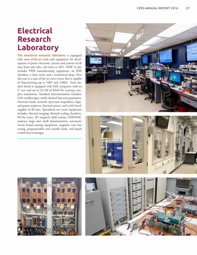
Electrical Research LaboratoryThe electrical research laboratory is equipped with state-of-the-art tools and equipment for devel-opment of power electronic circuits and systems of all sizes from sub-volts, sub-watts to 6kV, 1MW. It also includes PWB manufacturing equipment, an EMI chamber, a clean room and a mechanical shop. New this year is a state of the art curve tracer that is capable of characterizing up to 10kV and 1500A. Each stu-dent bench is equipped with Dell computers with an i7 core and up to 16 GB of RAM for running com-plex simulations. Standard instrumentation includes: GHz oscilloscopes, multi-channel function generators, electronic loads, network, spectrum, impedance, logic, and power analyzers, thermal sensors, and ac/dc bench supplies of all sizes. Specialized test room equipment includes: thermal imaging, thermal cycling chambers, Hi-Pot tester, 3D magnetic field scanner, EMI/EMC analyzer, large and small dynamometers, automatic circuit board routing equipment, magnetic core loss testing, programmable and variable loads, and liquid cooled heat-exchanger.
27CPES ANNUAL REPORT 2016
VIRGINIA TECH FACILITIES
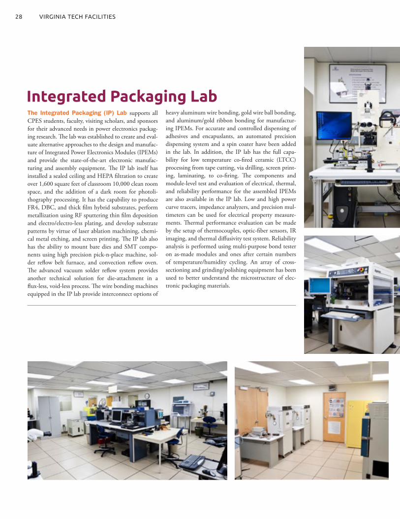
The Integrated Packaging (IP) Lab supports all CPES students, faculty, visiting scholars, and sponsors for their advanced needs in power electronics packag-ing research. The lab was established to create and eval-uate alternative approaches to the design and manufac-ture of Integrated Power Electronics Modules (IPEMs) and provide the state-of-the-art electronic manufac-turing and assembly equipment. The IP lab itself has installed a sealed ceiling and HEPA filtration to create over 1,600 square feet of classroom 10,000 clean room space, and the addition of a dark room for photoli-thography processing. It has the capability to produce FR4, DBC, and thick film hybrid substrates, perform metallization using RF sputtering thin film deposition and electro/electro-less plating, and develop substrate patterns by virtue of laser ablation machining, chemi-cal metal etching, and screen printing. The IP lab also has the ability to mount bare dies and SMT compo-nents using high precision pick-n-place machine, sol-der reflow belt furnace, and convection reflow oven. The advanced vacuum solder reflow system provides another technical solution for die-attachment in a flux-less, void-less process. The wire bonding machines equipped in the IP lab provide interconnect options of
heavy aluminum wire bonding, gold wire ball bonding, and aluminum/gold ribbon bonding for manufactur-ing IPEMs. For accurate and controlled dispensing of adhesives and encapuslants, an automated precision dispensing system and a spin coater have been added in the lab. In addition, the IP lab has the full capa-bility for low temperature co-fired ceramic (LTCC) processing from tape cutting, via drilling, screen print-ing, laminating, to co-firing. The components and module-level test and evaluation of electrical, thermal, and reliability performance for the assembled IPEMs are also available in the IP lab. Low and high power curve tracers, impedance analyzers, and precision mul-timeters can be used for electrical property measure-ments. Thermal performance evaluation can be made by the setup of thermocouples, optic-fiber sensors, IR imaging, and thermal diffusivity test system. Reliability analysis is performed using multi-purpose bond tester on as-made modules and ones after certain numbers of temperature/humidity cycling. An array of cross-sectioning and grinding/polishing equipment has been used to better understand the microstructure of elec-tronic packaging materials.
Integrated Packaging Lab
28
The computer lab supports all major software used in power electronics design including: SPICE, Sa-ber, Simplis, Code Composer, Math products – Mat-lab and Mathcad, Ansys Products – Workbench and Mechanical, Ansys Electromagnetics – Maxwell, Elec-tronics Desktop (Q3D, HFSS), Simplorer, SIWave, Mentor Graphics Flowtherm, PLECS, and Altium Designer.
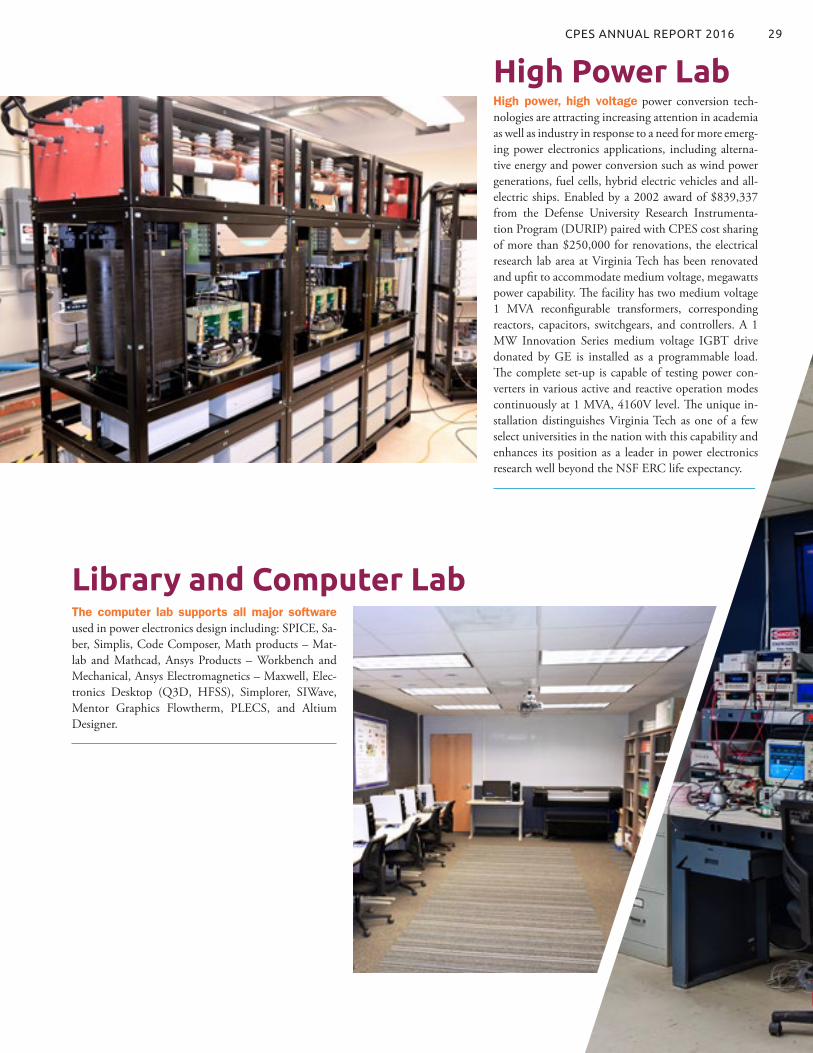
High power, high voltage power conversion tech-nologies are attracting increasing attention in academia as well as industry in response to a need for more emerg-ing power electronics applications, including alterna-tive energy and power conversion such as wind power generations, fuel cells, hybrid electric vehicles and all-electric ships. Enabled by a 2002 award of $839,337 from the Defense University Research Instrumenta-tion Program (DURIP) paired with CPES cost sharing of more than $250,000 for renovations, the electrical research lab area at Virginia Tech has been renovated and upfit to accommodate medium voltage, megawatts power capability. The facility has two medium voltage 1 MVA reconfigurable transformers, corresponding reactors, capacitors, switchgears, and controllers. A 1 MW Innovation Series medium voltage IGBT drive donated by GE is installed as a programmable load. The complete set-up is capable of testing power con-verters in various active and reactive operation modes continuously at 1 MVA, 4160V level. The unique in-stallation distinguishes Virginia Tech as one of a few select universities in the nation with this capability and enhances its position as a leader in power electronics research well beyond the NSF ERC life expectancy.
High Power Lab
Library and Computer Lab
29CPES ANNUAL REPORT 2016

SPOTLIGHT ON ALUMNIAffiliation: Flextronics International - FlexPowerPosition title: VP of EngineeringLast degree from Virginia Tech: Ph.D.Year Graduated: 1994
CAREER HIGHLIGHTS1994: Member of Technical Staff, Lucent Technologies1998: Technical Manager, Distinguished Member of
Technical Staff, Lucent Technologies2001: VP of Engineering & one of original founding
members, Innoveta Technologies 2003: VP of Engineering, TDK Innoveta, Inc. (Innoveta
acquired by TDK) 2005: Chief Technical Officer, Emerson Network Power -
Embedded Power2009: General Manager, Delta Electronics – China New
Energy/Megawatt/Wind Power BU2014: VP of Engineering, Flextronics International –
FlexPower
QUOTE
“The graduate study at VPEC changed my life profoundly. The center created an environment that is characterized by intellectual stimuli and team spirit. It was an enjoyable place to study and work. Thanks to Dr. Lee, all the faculty and staff, and fellow students, I learned so much during my stay at VPEC, which laid a solid foundation for my professional career in various companies and dif-ferent geographical locations.”
Chen, Qing (Que)Affiliation: Silergy Corp.Position title: CEOLast degree from Virginia Tech: Ph.D.Year Graduated: 1998
CAREER HIGHLIGHTS1995-1998: VPT Inc. : Design Engineer1998-2003: Linear Technology Corp. : Applications
Engineer/Section Manager, Developed industry first power module chip
2004-2007: Monolithic Power System: VP of System and Applications
2008-now: Silergy Corp.: Founder and CEO, founded the analog IC design house in 2008, brought the company IPO in 2013 and achieved $148M revenue in 2015
QUOTE
“Over decades, VPEC/CPES has persistently pursued the best power conversion technologies to achieve the highest efficiency and power den-sity. The single-minded approach has guided me throughout my career and contributed to business success.”
Chen, Wei
30

Affiliation: Inventronics. Inc.Position title: CEOLast degree from Virginia Tech: Ph.D.Year Graduated: 1993
Affiliation: Delta Products CorporationPosition title: Senior Vice President R&DLast degree from Virginia Tech: Ph.D.Year Graduated: 1988
CAREER HIGHLIGHTS1993: Cofounded VPT with Dr. Fred Lee and Dr. Dan
Sable1999: Founded e-Power Co., Ltd. in Hangzhou, China2001: Sold e-Power to Bel Fuse Inc. which is a NASDAQ
listed company 2007: Founded Inventronics Inc. in Hangzhou China 2009: Selected as member of China One Thousand
Elite Program2011: Elected as Top 20 China CCTV Economy Person
of the Year
CAREER HIGHLIGHTS1976: Research Assistant, University of Novi Sad,
Yugoslavia1988: Research Scientist, Virginia Tech1991: Director, Delta Power Electronics Lab.,
Blacksburg, VA1998: Vice President R&D, Delta Products Corporation,
Research Triangle Park, NC 2001: Fellow IEEE2004: CTO, Delta Power Supply Business Group2015: National Academy of Engineering
QUOTE
“In hindsight, joining the Power Electronics Re-search Group (PERG) at Virginia Tech led by Dr. Lee has been the defining moment of my career. Besides receiving an outstanding power electron-ics education, as a member of PERG, I was given the opportunity to perform cutting-edge research for leading technology companies and government entities. This involvement helped me discover the satisfaction of innovative work that has been the major inspiration for dedicating my entire career to R&D.”
Hua, Gary Jovanovic, Milan M.
31CPES ANNUAL REPORT 2016

Affiliation: Intel CorporationPosition title: VP/FellowLast degree from Virginia Tech: Ph.D.Year Graduated: 1993
Affiliation: Texas InstrumentsPosition title: Business Unit Manager, Battery Charging ProductsLast degree from Virginia Tech: Ph.D.Year Graduated: 1997
CAREER HIGHLIGHTS2003: Apps Manager, at Intersil Corp2005: Apps manager, elected as Senior Member of
Technical Staff, Texas Instruments2007: Elected as Distinguished Member of Technical
Staff at Texas Instruments2011: Named as Asian American Engineer of the Year
Awards (AAEOY) by Chinese Institute of Engi-neers (CIE)
2011: Product Line Manager, Texas Instruments2016: Business Unit Manager / General Manager, Bat-
tery Charging Products, Texas Instruments
CAREER HIGHLIGHTS1993-1998: Member of the Technical Staff, Power
Systems Research Dept., AT&T Power Systems
1998-2000: Department Head, Power Systems Re-search Dept., Bell Laboratories, Lucent Technologies
2000-2002: Director, Analog and Power Management Research, Bell Laboratories, Lucent Tech-nologies
2002-2013: Founder, President and CEO, Enpirion Inc.2014-2016: Chief Technology Officer, Power Products
Business, Altera Corporation2016: VP / Fellow, Intel Corporation
QUOTE
QUOTE
“VPEC and Professor Lee’s luminary leadership have been the primary drivers forging my pas-sion for this field of power electronics and more importantly my intense commitment to continue its advancement with innovative technologies. It was the broad spectrum of projects, new technolo-gies, advanced lab capabilities, industry sponsor-ships and most importantly the open, undictated, creative research direction at VPEC that laid the foundation for me to continue to technologically advance the field many years after graduating. I am very proud to say that my entire career has been a direct and continuous advancement on the themes of my early research years at VPEC. Look-ing back today, Virginia Tech has been a profound pillar in my professional career, one I am certain could not have been achieved at any other Univer-sity anywhere else in the world. I would never have it any other way.”
“Learn not only knowledge, but more importantly learn how to lead, drive, collaborate, and com-municate with the teams for achieving challenging goals.”
Lotfi, Ashraf Qian, Jinrong
SPOTLIGHT ON ALUMNI32

Affiliation: VPT Inc.
Position title: CEO
Last degree from Virginia Tech: Ph.D.
Year Graduated: 1991
Affiliation: FSP-Powerland Technology Inc.
Professor of Xi’an Jiaotong University
Professor of Nanjing Uni-versity of Aeronautics and Astronautics
Position title: CEO
CPES Affiliation: Associate Professor
QUOTE
QUOTE
“The experience from CPES has been invaluable both in my professional and academic career. Professionally, the CPES experience gives instant credibility in the market to VPT customers. Since the start, VPT has hired about 20 engineers who have received a Bachelors, Masters, or PhD from Virginia Tech. The experience has been overwhelmingly positive. Academically, the CPES experience is something that I can share with my ECE students, many of whom strive to become CPES members.”
“Other than comprehensive power electronics knowledge learned in CPES, the professional methodology and research philosophy is the most important part we gained in CPES, which ensures right process and solid work with reasonable value attitude.”
Sable, Dan Xu, Ming
CAREER HIGHLIGHTS1978: Started career as a co-op student with RCA
Astro-Electronics, then went full-time1980: Received BS from MIT in Electrical Engineering1985: Started Teaching Electrical Engineering at
Trenton State College1991: Received PhD from VPEC1993: Co-Founded VPT with Dr. Fred Lee
and Dr. Gary Hua1997: Established Joint Venture with Delta Electronics
on Hi-Rel DC-DC Converters2001: Received Class H Certification from US Military
for hybrid DC-DC Converters2005: Launch of first GPS Satellite powered
with VPT DC-DC Converters 2009: Orchestrated sale of VPT to Heico Corp (NYSE:
HEI)2012: Moved VPT into new building at the VT Corporate
Research Center2012: Appointed Adjunct Prof. of Practice in the ECE
Dept. (Teach 1 class/semester)2013: Acquired Radiation Test Facility (VPT Rad)
in Boston, MA 2015: Grown VPT to #1 worldwide in Hi-Rel DC-DC
Converter Standard Products
CAREER HIGHLIGHTS2006: Associate professor with Virginia Tech2006: Guest professor with Xian Jiaotong University2007: Guest Professor with Nanjing University of Aero-
nautics and Astronautics2009: CEO of FSP-Powerland Technology Inc.2010: Developed the first 90+ efficiency silver box
power supply in the world, which established the “80 plus” platinum efficiency standard of desktop PSU in the world
2011: Elected into “Thousand Experts” plan of Chinese government
2013: Developed the smallest 65W laptop adaptor in the world and brought the wall-mount laptop adaptor concept into the industry
2013: Chairman of FSP-Powerland Technology Inc. 2015: FSP-Powerland has been a company develop-
ing advanced technologies and customizing leading-edge products for challenging electronics applications with power ranging from 10w up to 500kw. As one of its core business, FSP-Power-land works with over 20 international companies by providing contract-project service, with over 2-million US funding every year. FSP-Powerland has become the largest power electronics design house in China. Among its 80+ engineers, there are more than 40 masters and 7 PhDs, including 5 PhDs from CPES.
33CPES ANNUAL REPORT 2016

Affiliation: GE Power Conversion
Position title: Product Platform Leader, China/Executive Technology
Last degree from Virginia Tech: Ph.D.
Year Graduated: 1998
CAREER HIGHLIGHTS1998-2001: Senior Engineer, GE Global
Research Center2001-2008: Lab Manager, GE Global Research Center2008-2011: Global Electrification Leader/Executive
Engineering, GE Oil & Gas2011-2012: Technology & Product Integration Leader
for Converteam acquisition, GE2012-2014: Global Technology & Value Engineering
Leader/Executive Technology, GE Power Conversion
2013-now: Chairman, Board of Directors, Powerex2017-now: Co-Chair, Industrial Advisory Board, CPES2014-now: Product Platform Leader, China,
GE Power Conversion
QUOTE
“So much great learning at VPEC/CPES from professors, staff, bright minds of fellow students, close link with industry deeply imprinted and became second nature in my career:• Strive to excel with dedication and pride• Always explore innovative technology bound-
ary for things that matter • Leadership, team work and collaboration• Communication, communication,
communication – from articulating technology and value story to influencing people around
• Walk the talk, accountability, deliver to make impact
Four years at VPEC/CPES take the most special place in my memory … full of fun and stories.”
Zhang, Richard
SPOTLIGHT ON ALUMNI34

Dushan BoroyevichCPES Co-Director
American Electric Power Professor (ECE)
Dushan Boroyevich was born in 1952 in Zagreb, Croatia, in what then used to be Yugoslavia.
In the same country, he earned a Dipl. Ing. degree from the University of Belgrade in 1976 and an M.S. degree from the University of Novi Sad in 1982, both in electrical engineering. He obtained a Ph.D. degree in power electronics in 1986 from Virginia Polytechnic Institute and State University.
Fred C. LeeCPES Co-Director
University Distinguished Professor (ECE)
Fred C. Lee received his B.S. degree in electrical engineering from the National Cheng Kung University in Taiwan in 1968, and his M.S.
and Ph.D. degrees in electrical engineering from Duke University in 1972 and 1974, respectively. As CPES Director, Dr. Lee leads a program that encompasses research, technology development, educational outreach, industry collaboration, and technology transfer.
Faculty
PEOPLE
Khai NgoProfessor (ECE)
Khai Ngo received his B.S. degree from Cali-fornia State Polytechnic University, Pomona, in 1979, and his M.S. and Ph.D. degrees from the California Institute of Technology, Pasadena,
in 1980 and 1984, respectively, all in Electrical and Electronics Engineering. At Virginia Tech, he pursues technologies for integration and packag-ing of power passive and active components to re-alize building blocks for power electronic systems.
Rolando BurgosAssociate Professor (ECE)
Rolando Burgos (S’96–M’03) was born in Concepcion, Chile, where he attended the University of Concep-cion, earning his B.S.
in Electronics Engineering in 1995 and a Pro-fessional Engineering Certificate in Electronics Engineering in 1997, graduating with honors. At the same institution he later earned his M.S. and Ph.D. degrees in Electrical Engineering in 1999 and 2002, respectively.
Qiang LiAssistant Professor (ECE)
Qiang Li received his B.S. degree in 2003 and M.S. degree in 2006 from Zhejiang University. Then in 2011 he received his Ph.D. from Virginia Tech. He started at Virginia Tech as a Research Assistant Professor in 2011 and was promoted to Assistant Professor in 2012. His research interests include high-density electronics packaging and integration, high-frequency magnetic components, high-frequency power conversion, distributed power syustems, and renewable energy.
35CPES ANNUAL REPORT 2016

Marianne Hawthorne
Igor Cvetkovic
Linda Long
David Gilham
Trish Rose Teresa Shaw
Technical staff
Support staff
Guo-Quan Lu
Wenli Zhang Mingkai Mu Zhiyu Shen Xuning Zhang
Affiliatefaculty
Researchfaculty Research scientists
PEOPLE Faculty/Visiting scholars36

Visiting scholars
Cai, Chaofeng VISITING ENGINEERDelta Electronics,China
Delhommais, Mylène M.S. STUDENTGrenoble-INP Ense3 Laboratoire, France
Dewar, David STUDENT INTERNUniversity of Notting-ham, UK
Du, Weijing POSTDOCZhejiang University, China
Emori, Kenta VISITING ENGINEERNissan Motor Co., Ltd., Japan
Hu, PeiqingVISITING ENGINEERDelta Electronics,China
Jonishi , Akihiro VISITING ENGINEERFuji Electric Co., Ltd.,Japan
Karwatzki, Dennis PH.D. STUDENTLeibniz Universität Hannover, Germany
Kim, Rae-YoungPROFESSORHanyang University,Korea
Li, Kai PH.D. STUDENTTsinghua University, China
Li, Yan-Cun (Daniel)POSTDOCNational Taiwan University, Taiwan
Liu, Zeng PROFESSOR/ RESEARCHERXi’an Jiaotong University (XJTU), China
Perrin, RemiPH.D. STUDENTLaboratoire AMPERE (SAFRAN), France
Quentin, NicolasPH.D. STUDENTLaboratoire AMPERE (SAFRAN), France
Reusch, DavidVISITING ENGINEEREfficient Power Conver-sion, USA
37CPES ANNUAL REPORT 2016

Rizzoli, GabrielePH.D. STUDENTUniversity of Bologna,Italy
Shin, Jong-WonPOSTDOCSeoul National University, Korea
Sun, KeyaoM.S. STUDENTETH Zurich, Switzerland
Tanaka, KenichiroVISITING ENGINEERPanasonic Corporation, Japan
Vasquez Quintero, Juan Carlos POSTDOC/ASSISTANT PROFESSORAalborg University, Denmark
Wang, LiPROFESSOR Nanjing University of Aeronautics & Astronau-tics, China
Wang, YifengLECTURERTianjin University, China
Xiao, FurongPH.D. STUDENTBeijing Institute of Technology, China
Yang, RongfengPROFESSORHarbin Institute of Technology, China
Yue, Xiaolong PH.D. STUDENTXi’an Jiaotong UniversityChina
Yuki, SeiyaVISITING ENGINEER DOWA Metaltech Co., Ltd., Japan
Zheng, LiranSTUDENT INTERNTsinghua University, China
PEOPLE Visiting scholars/Students38

Acken, Robert
Chen, Fang
Feng, Junjie
Ahmed, Mohamed
Chu, Alex
Gao, Shan
Bari, Syed
Cui, Han
Gadelrab, Rimon
Bhagwat, Gitesh
DiMarino, Christina
Ge, Ting
Chen, Chien-An
Fei, Chao
Haryani, Nidhi
Students
Hou, Dongbin Hou, Xueyu Hsieh, Yi-Hsun Huang, Xiucheng Huang, Zhengrong
39CPES ANNUAL REPORT 2016

Li, Bin
Liu, Xingye
Marzoughi, Alinaghi
Romero, Amy
Li, Chen
Liu, Zhengyang
Miao, Zichen
Sun, Bingyao Sun, Weizhen (Abby) Tang, Ye Wang, Jun
Li, Chi
Lu, Ming
Ohn, Sungjae
Li, Qian
Lyu, Yadong
Qin, Ruiyang
Li, Virginia
Mao, Yincan
Rashidi Mehrabadi, Niloofar
StudentsPEOPLE40
Wang, Qiong
Yu, Jianghui
Xu, Kuangzhe
Zhang, Lujie
Xu, Yue
Zhao, Shishuo
Yan, Yasmine Yang, Yuchen
Xue, Lingxiao
Jiao, Yang
Zhang, Wei
Liu, Pei-Hsin
Zheng, Hanguang
Najmi, Vahid Tian, Shuilin
Graduates
Danilovic, MilisavEmployer: WiTricity Corporation
Employer: Delta Products Corporation
Employer: Texas Instruments
Employer: Texas Instruments
Employer: IBM
Employer: Solectria Employer: Linear Technology
Employer: Navitas Semiconductor
41CPES ANNUAL REPORT 2016

Ralph CavinSemiconductor Research Corporation (retired)
John KassakianMassachusetts Institute of Technology
Tom LipoUniversity of Wisconsin-Madison (retired)
Bob SteigerwaldGE Global Research (retired)
Al TuckerOffice of Naval Research (retired)
Scientific Advisory Board (SAB)
Industry Advisory Board (IAB)Richard Zhang (IAB Chair)
GE Power Conversion
Milan Jovanovic (IAB Co-Chair)
Delta Electronics, Inc.
Paul Baude 3M Company
Uwe Badstuebner ABB, Inc.
Colin Lin AcBel Polytech, Inc.
Daniel Cadet ALSTOM Transport
Matt Wilkowski Altera - Enpirion Power
Ming-Ho Huang Chicony Power Technology Co., Ltd.
Wei Kong China National Electric Apparatus Re-search Institute
Ernie Parker Crane Aerospace & Electronics
Gerald Stanley Crown International
Catharine Huang CSR Zhuzhou Institute Co., Ltd.
Hiroshi Tomikawa Dowa Metaltech Co., Ltd.
Nils Backman Eltek
Mei-Ling Chiang Emerson Network Power
Laszlo Balogh Fairchild Semiconductor Corporation
Chingchi Chen Ford Motor Company
Rui Zhou GE Global Research
Ronald Young General Motors
Alain Coutrot Groupe SAFRAN
Dianbo Fu Huawei Technologies
Jiangqi He Intel
Tim McDonald International Rectifier/Infineon
Gary Hua Inventronics
Ivan Jadric Johnson Controls, Inc.
Dennis Gyma Keysight Technologies
Pei-Yuan Peng LG Electronics China R&D Center
Henry Zhang Linear Technology
Karen Duneman Lockheed Martin Corporation
Joe Chang Macroblock, Inc.
Laurentiu Olariu Microsoft Corporation
Tatsuo Bizen Murata Manufacturing Co., Ltd.
Tetsuya Hayashi Nissan Motor Co., Ltd.
Jeff Pearse ON Semiconductor
Bob Galli Panasonic Corporation
Don Yuh Richtek Technology
Richard Lukaszewski
Rockwell Automation
Sebastian Nielebock
Siemens Corporate Research
Mark Gerlovin Sonos, Inc.
Hirotaka Oomori Sumitomo Electric Industries, Ltd.
Brian Carpenter Texas Instruments
Yusuke Hazama Toshiba Corporation
Luis Arnedo United Technologies Research Center
Jianping Zhou ZTE Corporation
Advisory boardsPEOPLE42

HONORS & ACHIEVEMENTSNational and International HonorsRolando Burgos served as General Chair of the 3rd IEEE Workshop on Wide Bandgap Power Devices and Applications (WiPDA 2015), hosted by CPES at Virginia Tech, November 2-4, 2015
CPES-Virginia Tech, Memorandum of Understanding (MOU) with NPERC-J (New Generation of Power Electronics and System Research Consortium Japan)
Dushan BoroyevichHonorary Professor Xi’an Jiaotong University, Xi’an, China
Dushan Boroyevich, Member of International Academic Committee, State Key Laboratories of Electrical Insulation and Power EquipmentXi’an Jiaotong University, Xi’an, China
Keynote AddressesFred C. Lee, Keynote Speaker: “Packaging Considerations of GaN for High Fre-quency Applications,” International Workshop on Integrated Power Packaging (IWIPP), Chicago, Illinois, May 4-6, 2015
Dushan Boroyevich, Keynote Speaker: “From Power Electronics Devices to Electronic Power Systems – a CPES Perspective,” 2nd Annual Conference of UK Engineering and Physical Sciences Research Council (EPSRC), Centre for Power Electronics (CPE), University of Nottingham, United Kingdom, June 30, 2015
Invited Talks Dushan Boroyevich, Invited Speaker: “Intergrid: A Future Electronic Energy Network?” University of Illinois at Urbana-Champaign, February 2015
Dushan Boroyevich, Invited Speaker, “Overview of Research at CPES,” University of Toulouse, Toulouse, France, February 2015
Dushan Boroyevich, Invited Presentation: “Integrated Design by Optimization of Electrical Power Systems for More Electric Aircraft,” University of Toulouse, Toulouse, France, February 2015
Fred C. Lee, Distinguished Speaker: “Energy and Power Electronics,” Spring 2015 ECE Distinguished Colloquium Series hosted by Booz Allen Hamilton, University of Maryland, February 27, 2015
Fred C. Lee, Invited Tutorial: “Is GaN a Game Changing Device?” 2015 CPES Conference, Blacksburg, VA, April 12, 2015
Dushan Boroyevich, Invited Tutorial: “Is SiC a Game Changer?” 2015 CPES Conference, Blacksburg, VA, April 12, 2015
Khai Ngo, Invited Speaker: “Opportunities in Packaging and Integration for Wide-Bandgap Power Electronics,” 2015 International Conference on Electronics Packaging and iMAPS All Asia Conference (ICEP-IAAC), Kyoto, Japan, April 17, 2015
43CPES ANNUAL REPORT 2016

Fred C. Lee, Invited Speaker, “Sustainable Energy and Challenges in the 21st Century,” Illinois Institute of Technology (ITT) Distinguished Lecture Series, May 6, 2015
Dushan Boroyevich, Invited Speaker, “The CPES Experience,” Opening Ceremony of NPERC-J, Tokyo, Japan, May 27, 2015
Dushan Boroyevich, Invited Presentation, “A Nonlinear Droop Method to Improve Voltage Regulation and Load Sharing in DC Systems,” 2015 IEEE First International Conference on Direct Current Microgrids (ICDCM), June 7-10, 2015, Atlanta, GA
Dushan Boroyevich, Invited Speaker, “Is SiC a Game Changer?” The Electronics, Power and Energy Conversion Group, University of Cambridge, Cambridge, United Kingdom, July 2, 2015
Dushan Boroyevich, Invited Speaker, “Is SiC a Game Changer?” Electrical Energy Management Research Group, University of Bristol, Bristol, United Kingdom, July 3, 2015
Fred C. Lee, Invited Speaker, “Sustainable Energy and Challenges in the 21st Century,” Tsinghua University, Beijing, China, July 23, 2015
Dushan Boroyevich, Invited Speaker, “Overview of Research,” Department of Electrical, Electronic and Information Engineering “Guglielmo Marconi” – DEI, Università di Bologna, Italy, September 2, 2015
Dushan Boroyevich, Invited Speaker, “High-Density Power Electronics for Grid-Scale Ap-plications,” State Key Laboratory of Electrical Insulation and Power Equipment, Xi’an Jiaotong University, Xi’an, China, October 23, 2015
Dushan Boroyevich, “More Electric Grid – Per-formance Enhancement or Stability Nightmare?” Power Electronics and Renewable Energy Re-search Center (PEREC), Xi’an Jiaotong University, Xi’an, China, October 26, 2015
Dushan Boroyevich, “Overview of Research,” Department of Electrical Engineering, Tsinghua University, Beijing, China, October 27, 2015
Dushan Boroyevich, “Intergrid: A Future Elec-tronic Power System?” State Grid Corporation of China, Beijing, China, October 28, 2015
Fred C. Lee, Invited Speaker, “Design for Manu-facturability,” Emerson Network Power, Shenzhen, China, October 29, 2015.
Fred C. Lee, Invited Speaker, “Sustainable En-ergy & Challenges in the 21st Century,” Power Electronics Forum, ECE Department, National Cheng Kung University, Tainan City, Taiwan, Octo-ber 30, 2015
Dushan Boroyevich, “Overview of Research on Renewable Energy and Nanogrids,” Huawei Tech-nologies, Shenzhen, China, October 30, 2015
Fred C. Lee, Invited Speaker as Honorary Chair, “Green Energy,” 2015 International Future Energy Electronics Conference (IFEEC), Taipei, Taiwan, November 1-4, 2015
Dushan Boroyevich, Invited Tutorial, “Is SiC a Game Changer?” 13th Brazilian Power Electron-ics Conference (COBEP) and 1st Southern Power Electronics Conference (SPEC), Fortaleza, Brazil, November 29, 2015
2015 CPES Annual Conference Best Student Presentation AwardsBest Technical Presentation Award Yang Jiao
Best Dialogue Presentation Awards Christina DiMarinoXiucheng HuangNiloofar RashidiLingxiao Xue
HONORS & ACHIEVEMENTS44

PUBLICATIONSTransactions PapersSurvey of High-Temperature Polymeric Encapsulants for Power Electronic PackagingYiying Yao, Guo-Quan Lu, Dushan Boroyevich, Khai D. T. NgoIEEE Transactions on Components, Packaging, and Manufacturing Technology, Vol. 5, No. 2, February 2015, pp. 168-181
High-Density Integration of High-Frequency High-Current Point-of-Load (POL) Modules with Planar InductorsWenli Zhang, Yipeng Su, Mingkai Mu, David Gilham, Qiang Li, Fred C. LeeIEEE Transactions on Power Electronics, Vol. 30, No. 3, March 2015, pp. 1421-1431
Small-Signal Analysis and Optimal Design of Constant Frequency V2 ControlShuilin Tian, Fred C. Lee, Paolo Mattavelli, Yingyi YanIEEE Transactions on Power Electronics, Vol. 30, No. 3, March 2015, pp. 1724-1733
LCL Filter Design and Inductor Current Ripple Analysis for a Three-Level NPC Grid Interface ConverterYang Jiao, Fred C. LeeIEEE Transactions on Power Electronics, Vol. 30, No. 9, September 2015, pp. 4659-4668
Small-Signal Stability Analysis of Three-Phase AC Systems in the Presence of Constant Power Loads Based on Measured D-Q Frame ImpedancesBo Wen, Dushan Boroyevich, Rolando Burogs, Paolo Mattavelli, Zhiyu ShenIEEE Transactions on Power Electronics, Vol. 30, No. 10, October 2015, pp. 5952 - 5963
New Modulation Scheme for 3-Level Active Neutral Point Clamped Converter with Loss and Stress ReductionYang Jiao, Fred C. LeeIEEE Transactions on Industrial Electronics, Vol. 62, No. 9, September 2015, pp. 5468-5479
Multichannel LED Driver with CLL Resonant ConverterXuebing Chen, Daocheng Huang, Qiang Li, Fred C. LeeIEEE Journal of Emerging and Selected Topics in Power Electronics, Vol. 3, No. 3, September 2015, pp. 589-598
Characterization and Enhancement of High-Voltage Cascode GaN DevicesXiucheng Huang, Zhengyang Liu, Fred C. Lee, Qiang LiIEEE Transactions on Electron Devices (invited Paper), Vol. 62, No. 2, February 2015, pp. 270-277
High-Temperature Silicon Carbide: Characterization of State-of-the-Art Silicon Carbide Power TransistorsChristina DiMarino, Rolando Burgos, Dushan BoroyevichIEEE Industrial Electronics Magazine, Vol. 9, No. 3, September 2015, pp. 19-30
Thermal Analysis and Improvement of Cascode GaN Device Package for Totem-Pole Bridgeless PFC RectifierShuojie She, Wenli Zhang, Zhengyang Liu, Fred C. Lee, Xiucheng Huang, Weijing Du, Qiang LiApplied Thermal Engineering, Volume 90, November 2015, pp. 413-423
Avoiding Si MOSFET Avalanche and Achieving Zero-Voltage-Switching for Cascode GaN DevicesXiucheng Huang, Weijing Du, Fred C. Lee, Qiang Li, Zhengyang LiuIEEE Transactions on Power Electronics, Vol. 31, No. 1, January 2016, pp. 593-600
45CPES ANNUAL REPORT 2016

Impedance-Based Analysis of Grid-Synchronization Stability for Three-Phase Paralleled Converters Bo Wen, Dong Dong, Dushan Boroyevich, Rolando Burgos, Paolo Mattavelli, Zhiyu ShenIEEE Transactions on Power Electronics, Vol. 31, No. 1, January 2016, pp. 26-38
Impedance-Based Analysis of Active Frequency Drift Islanding Detection for Grid-Tied Inverter System Bo Wen, Dushan Boroyevich, Rolando Burgos, Zhiyu Shen, Paolo MattavelliIEEE Transactions on Industry Applications, Vol. 52, No. 1, January/February 2016, pp. 332-341
Advances in Power Conversion and Drives for Shipboard Systems (Invited Paper) Fei Wang, Zheyu Zhang, Terry Ericsen, Ravisekhar Raju, Rolando Burgos, Dushan BoroyevichProceedings of the IEEE, Vol. 103, No. 12, December 2015, pp. 2285-2311
Dual Active Bridge-Based Battery Charger for Plug-in Hybrid Electric Vehicle with Charging Current Containing Low Frequency Ripple Lingxiao Xue, Zhiyu Shen, Dushan Boroyevich, Paolo Mattavelli, Daniel Diaz IEEE Transactions on Power Electronics, Vol. 30, No. 12, December 2015, pp. 7299-7307
Analysis of D-Q Small-Signal Impedance of Grid-Tied Inverters Bo Wen, Dushan Boroyevich, Rolando Burgos, Paolo Mattavelli, Zhiyu Shen IEEE Transactions on Power Electronics, Vol. 31, No. 1, January 2016, pp. 675-687
Conference PapersTowards More Optimization for Aircraft Energy Conversion Systems Alain Tardy, X. Roboam, Pericle Zanchetta, Dushan Boroyevich, Rolando Burgos, Jeau-Luc Schanen, F. Wurtz, B. Sareni, Patrick Wheeler Proceedings, MEA 2015, Toulouse,France, February 2015
Analysis of Dead Time Influence on Common Mode Volt-Second and Inductor Saturation in Three-Phase DC-Fed Motor Drive SystemsXuning Zhang, Dushan Boroyevich, Rolando Burgos2015 APEC (29th Annual IEEE Applied Power Electronics Conference & Exposition), Charlotte, NC, March 15-19, 2015
Reliability Modeling of Capacitor Bank for Modular Multilevel Converter Based on Markov State-Space ModelVahid Najmi, Jun Wang, Rolando Burgos, Dushan Boroyevich2015 APEC (29th Annual IEEE Applied Power Electronics Conference & Exposition), Charlotte, NC, March 15-19, 2015
A New Modeling Approach for Modular Multilevel Converter (MMC) in D-Q FrameVahid Najmi, Rolando Burgos, Nawaf NazirVahid Najmi, Rolando Burgos, Nawaf Nazir
D-Q Impedance Specification for Balanced Three-Phase Distributed Power SystemBo Wen, Dushan Boroyevich, Rolando Burgos, Paolo Mattavelli, Zhiyu Shen2015 APEC (29th Annual IEEE Applied Power Electronics Conference & Exposition), Charlotte, NC, March 15-19, 2015
Small-Signal Impedance Measurement in Medium Voltage DC Power Systems Zhiyu Shen, Marko Jaksic, Igor Cvetkovic, Rolando Burgos, Dushan Boroyevich 2015 International Conference on Electrical Systems for Aircraft, Railway, Ship Propulsion and Road Vehicles (ESARS), RWTH University Campus, Aachen, Germany, March 3-5, 2015
Improving the Efficiency and Dynamics of 3D Integrated POLDongbin Hou, Yipeng Su, Qiang Li, Fred C. Lee2015 APEC (29th Annual IEEE Applied Power Electronics Conference & Exposition), Charlotte, NC, March 15-19, 2015
MHz GaN-Based Interleaved CRM Bi-Directional Buck/Boost Converter with Coupled InductorXiucheng Huang, Fred C. Lee, Qiang Li, Weijing Du2015 APEC (29th Annual IEEE Applied Power Electronics Conference & Exposition), Charlotte, NC, March 15-19, 2015
DBC Switch Module for Management of Temperature and Noise in 220-W/in3 Power AssemblyJongwon Shin, Woochan Kim, Khai D. T. Ngo2015 APEC (29th Annual IEEE Applied Power Electronics Conference & Exposition), Charlotte, NC, March 15-19, 2015
GaN-Based High Frequency Totem-Pole Bridgeless PFC Design with Digital ImplementationLingxiao Xue, Zhiyu Shen, Dushan Boroyevich, Paolo Mattavelli2015 APEC (29th Annual IEEE Applied Power Electronics Conference & Exposition), Charlotte, NC, March 15-19, 2015
PUBLICATIONS Trasaction Papers/Conference Papers46

The Optimal Design of GaN-Based Dual Active Bridge for Bi-Directional Plug-In Hybrid Electric Vehicles (PHEV) ChargerLingxiao Xue, Mingkai Mu, Dushan Boroyevich, Paolo Mattavelli2015 APEC (29th Annual IEEE Applied Power Electronics Conference & Exposition), Charlotte, NC, March 15-19, 2015
Variable Frequency and Constant Frequency Modulation Techniques for GaN Based MHz H-Bridge PFCNidhi Haryani, Rolando Burgos, Dushan Bororyevich2015 APEC (29th Annual IEEE Applied Power Electronics Conference & Exposition), Charlotte, NC, March 15-19, 2015
Soft Start-Up for High Frequency LLC Resonant Converter with Optimal Trajectory ControlChao Fei, Fred C. Lee, Qiang Li2015 APEC (29th Annual IEEE Applied Power Electronics Conference & Exposition), Charlotte, NC, March 15-19, 2015
Analysis and Design of Coupled Inductor for Interleaved Multiphase Three-Level DC-DC ConvertersMingkai Mu, Fred C. Lee, Yang Jiao, Sizhao Lu2015 APEC (29th Annual IEEE Applied Power Electronics Conference & Exposition), Charlotte, NC, March 15-19, 2015
Design of Integrated Transformer and Inductor for High Frequency Dual Active Bridge GaN Charger for PHEVMingkai Mu, Lingxiao Xue, Dushan Boroyevich, Brian Hughes, Paolo Mattavelli2015 APEC (29th Annual IEEE Applied Power Electronics Conference & Exposition), Charlotte, NC, March 15-19, 2015
Fast Adaptive On-Time Control Method for Transient Performance ImprovementSyed Bari, Qiang Li, Fred C. Lee2015 APEC (29th Annual IEEE Applied Power Electronics Conference & Exposition), Charlotte, NC, March 15-19, 2015
Design and Implementation of Interleaved Vienna Rectifier with Greater Than 99% EfficiencyQiong Wang, Xuning Zhang, Rolando Burgos, Dushan Boroyevich, Adam White, Mustansir Kheraluwala2015 APEC (29th Annual IEEE Applied Power Electronics Conference & Exposition), Charlotte, NC, March 15-19, 2015
Model-Predictive Control to Realize the Switching-Cycle Capacitor Voltage Control for the Modular Multilevel ConvertersJun Wang, Rolando Burgos, Dushan Boroyevich2015 APEC (29th Annual IEEE Applied Power Electronics Conference & Exposition), Charlotte, NC, March 15-19, 2015
Reliability-Oriented IGBT Selection for High Power ConvertersJun Wang, Vahid Najmi, Rolando Burgos, Dushan Boroyevich2015 APEC (29th Annual IEEE Applied Power Electronics Conference & Exposition), Charlotte, NC, March 15-19, 2015
Assessment of Switching Frequency Impact on the Prediction Capability of Common-Mode EMI Emissions of SiC Power Converters Using Unterminated Behavioral ModelsBingyao Sun, Rolando Burgos, Xuning Zhang, Hemant Bishnoi, Dushan Boroyevich2015 APEC (29th Annual IEEE Applied Power Electronics Conference & Exposition), Charlotte, NC, March 15-19, 2015, pp. 1153-1160
Multi-Phase Smart Converter for PV SystemZhongsheng Cao, Qiang Li, Fred C. Lee2015 APEC (29th Annual IEEE Applied Power Electronics Conference & Exposition), Charlotte, NC, March 15-19, 2015
Low Profile Coupled Inductor Substrate with Fast Transient ResponseYipeng Su, Dongbin Hou, Fred Lee, Qiang Li 2015 APEC (29th Annual IEEE Applied Power Electronics Conference & Exposition), Charlotte, NC, March 15-19, 2015
Switching-Cycle Capacitor Voltage Control for the Modular Multilevel DC/DC ConvertersJun Wang, Rolando Burgos, Dushan Boroyevich2015 APEC (29th Annual IEEE Applied Power Electronics Conference & Exposition), Charlotte, NC, March 15-19, 2015
Integrated Design by Optimization of Electrical Power Systems for More Electric Aircraft (Invited paper) Bo Wen, Xuning Zhang, Francis Effah, Arnaud Baraston, Pericle Zanchetta, Dushan Borojevich, Jean-Luc Schanen, Rolando Burgos, Patrick Wheeler, Alain Tardy Proceedings, MEA 2015, Toulouse, France, February 2015
Test Environment for a Novel Medium Voltage Impedance Measurement UnitFerenc Bogdan, John Hauer, James Langston, Karl Schoder, Mischa Steurer, Igor Cvetkovic, Zhiyu Shen, Marko Jaksic, Christina DiMarino, Fang Chen, Dushan Boroyevich, Rolando Burgos 2015 IEEE Electric Ship Technologies Symposium (ESTS), June 21-24, 2015, Old Town Alexandria, Virginia, pp. 99-103
47CPES ANNUAL REPORT 2016

Planar Inductor Structure with Variable Flux Distribution–a Benefit or Impediment?Yipeng Su, Qiang Li, Fred Lee, Dongbin Hou, Shuojie She2015 APEC (29th Annual IEEE Applied Power Electronics Conference & Exposition), Charlotte, NC, March 15-19, 2015
Opportunities in Packaging and Integration for Wide-Bandgap Power Electronics (Invited Presentation)Khai D.T. Ngo, Ting Ge, Ye Fan, Lujie Zhang, Hanguang ZhengICEP 2015 (International Conference on Electronics PackagingIAAC (iMAPS All Asia Conference), Kyoto, Japan, April 14-17, 2015; pp. 538-541
Effect of Heating Rate on Bonding Strength of Pressure-Free Sintered Nanosilver Joint (Invited)Kewei Xiao, Guangyin Lei, Khai D.T. Ngo, Guo-Quang LuICEP 2015 (International Conference on Electronics PackagingIAAC (iMAPS All Asia Conference), Kyoto, Japan, April 14-17, 2015; pp. 565-570
A New Package of High-Voltage Cascode Gallium Nitride Device for High-Frequency Applications (Invited Plenary)Fred C. Lee, Wenli Zhang, Xiucheng Huang, Zhengyang Liu, Weijing Du, Qiang LiIEEE International Workshop on Integrated Power Packaging (IWIPP 2015), Chicago, IL, May 3-6, 2015
A 50 kW SiC Three-Phase AC-DC Converter Design for High Temperature OperationZheng Chen, Ruxi Wang, Yiying Yao, Milisav Danilovic, Wenli Zhang, Christina DiMarino, Dushan Boroyevich, Rolando Burgos, Khai D.T. Ngo, Kaushik RajashekaraPCIM Europe 2015, May 19-21, 2015, Nuremberg, Germany, pp. 1239-1246
PUBLICATIONS
Modular Scalable Medium-Voltage Impedance Measurement Unit Using 10kV SiC MOSFET PEBBsI. Cvetkovic, Z. Shen, M. Jaksic, C. DiMarino, F. Chen, D. Boroyevich, R. Burgos In Proceed. IEEE ESTS 2015, pp. 326–331, June 2015
A Nonlinear Droop Method to Improve Voltage Regulation and Load Sharing in DC Systems (Invited Paper)Fang Chen, Rolando Burgos, Dushan Boroyevich, Wei Zhang2015 IEEE First International Conference on Direct Current Microgrids (ICDCM), June 7-10, 2015, Atlanta, GA
Model-Based Design of Modular Multilevel Converter with Minimized Design MarginsNiloofar Rashidi Mehrabadi, Rolando Burgos, Christopher Roy, Dushan Boroyevich2015 (Sixteenth) IEEE Workshop on Control and Modeling for Power Electronics (COMPEL), July 12-15, 2015, Vancouver, Canada
Active and Reactive Power Flow Analysis of a STATCOM with Virtual Synchronous Machine ControlChi Li, Rolando Burgos, Igor Cvetkovic, Dushan Boroyevich2015 (Sixteenth) IEEE Workshop on Control and Modeling for Power Electronics (COMPEL), July 12-15, 2015, Vancouver, Canada
Modeling and Control of Grid-Connected Voltage-Source Converters Emulating Isotropic and Anisotropic Synchronous MachinesIgor Cvetkovic, Dushan Boroyevich, Rolando Burgos, Chi Li, Paolo Mattavelli2015 (Sixteenth) IEEE Workshop on Control and Modeling for Power Electronics (COMPEL), July 12-15, 2015, Vancouver, Canada
Analysis of Capacitor Voltage Ripple Minimization in Modular Multilevel Converter Based on Average ModelAli Marzoughi, Rolando Burgos, Dushan Boroyevich, Yaosuo Xue2015 (Sixteenth) IEEE Workshop on Control and Modeling for Power Electronics (COMPEL), July 12-15, 2015, Vancouver, Canada
Assessment of Medium Voltage Distribution Feeders Under High Penetration of Photovoltaic GenerationYe Tang, Rolando Burgos, Chi Li, Dushan Boroyevich2015 (Sixteenth) IEEE Workshop on Control and Modeling for Power Electronics (COMPEL), July 12-15, 2015, Vancouver, Canada
Design of a Modular and Scalable Small-signal dq Impedance Measurement Unit for Grid Applications Utilizing 10 kV SiC MOSFETsZhiyu Shen, Igor Cvetkovic, Marko Jaksic, Christina DiMarino, Dushan Boroyevich, Rolando Burgos, Fang Chen17th European Conference on Power Electronics and Applications (EPE’15 ECCE Europe), Geneva, Switzerland, September 8-10, 2015
EMI Filter Design of DC-fed Motor-Drives Using Behavioral EMI ModelsHemant Bishnoi, Paolo Mattavelli, Rolando P. Burgos, Dushan Boroyevich17th European Conference on Power Electronics and Applications (EPE’15 ECCE Europe), Geneva, Switzerland, September 8-10, 2015
Conference Papers48

Wide-bandwidth Identification of Small-Signal dq Impedances of ac Power Systems via Single-Phase Series Voltage InjectionMarko Jaksic, Zhiyu Shen, Igor Cvetkovic, Dushan Boroyevich, Rolando Burgos, Paolo Mattavelli17th European Conference on Power Electronics and Applications (EPE’15 ECCE Europe), Geneva, Switzerland, September 8-10, 2015
Quantified Evaluation and Criteria Analysis for Distributed MPPT PV SystemFeng Wang, Fred C. Lee, Xiaolong Yue, Fang Zhuo17th European Conference on Power Electronics and Applications (EPE’15 ECCE Europe), Geneva, Switzerland, September 8-10, 2015
Comparison and Selection of Magnetic Materials for Coupled Inductor used in Interleaved Three-level Multi-phase DC-DC ConvertersMingkai Mu, Fred C. Lee2015 IEEE Energy Conversion Congress & Expo (ECCE 2015), Montreal, Canada, September 20-24, 2015
Light Load Efficiency Improvement for High Frequency LLC Converters with Simplified Optimal Trajectory Control (SOTC)Chao Fei, Fred C. Lee, Qiang Li2015 IEEE Energy Conversion Congress & Expo (ECCE 2015), Montreal, Canada, September 20-24, 2015
Multi-step Simplified Optimal Trajectory Control (SOTC) for Fast Transient Response of High Frequency LLC ConvertersChao Fei, Fred C. Lee, Qiang Li2015 IEEE Energy Conversion Congress & Expo (ECCE 2015), Montreal, Canada, September 20-24, 2015
Small-signal Equivalent Circuit Model of Series Resonant ConverterShuilin Tian, Fred C. Lee, Qiang Li, Bin Li2015 IEEE Energy Conversion Congress & Expo (ECCE 2015), Montreal, Canada, September 20-24, 2015
A Novel Driving Scheme for Synchronous Rectifier in MHz CRM Flyback Converterse with GaN DevicesXiucheng Huang, Weijing Du, Fred C. Lee, Qiang Li2015 IEEE Energy Conversion Congress & Expo (ECCE 2015), Montreal, Canada, September 20-24, 2015
Common Mode EMI Reduction Technique for Interleaved MHz Critical Mode PFC Converter with Coupled InductorYuchen Yang, Mingkai Mu, Zhengyang Liu, Fred Lee, Qiang Li2015 IEEE Energy Conversion Congress & Expo (ECCE 2015), Montreal, Canada, September 20-24, 2015
Design of GaN-Based MHz Totem-pole PFC RectifierZhengyang Liu, Fred Lee, Qiang Li, Yuchen Yang2015 IEEE Energy Conversion Congress & Expo (ECCE 2015), Montreal, Canada, September 20-24, 2015
A New Current Mode Control for Higher Noise Immunity and Faster Transient Response in Multi-phase OperationSyed Bari, Qiang Li, Fred Lee2015 IEEE Energy Conversion Congress & Expo (ECCE 2015), Montreal, Canada, September 20-24, 2015
On Discussion of Mixed Mode Noise in H-Bridge ConvertersXuning Zhang, Dushan Boroyevich, Rolando Burgos2015 IEEE Energy Conversion Congress & Expo (ECCE 2015), Montreal, Canada, September 20-24, 2015
Discontinuous Pulse Width Modulation Methods with Neutral Point Voltage Balancing for Three Phase Vienna RectifiersXuning Zhang, Qiong Wang, Rolando Burgos, Dushan Boroyevich2015 IEEE Energy Conversion Congress & Expo (ECCE 2015), Montreal, Canada, September 20-24, 2015
Steady-State Analysis of Voltages and Currents in Modular Multilevel Converter Based on Average ModelAlinaghi Marzoughi, Rolando Burgos, Dushan Boroyevich, Yaosuo Xue2015 IEEE Energy Conversion Congress & Expo (ECCE 2015), Montreal, Canada, September 20-24, 2015
Investigation and Design of Modular Multilevel Converter in AFE Mode with Minimized Passive ElementsAlinaghi Marzoughi, Rolando Burgos, Dushan Boroyevich, Yaosuo Xue2015 IEEE Energy Conversion Congress & Expo (ECCE 2015), Montreal, Canada, September 20-24, 2015
Design and Comparison of Cascaded H-bridge, Modular Multilevel Converter and 5-L Active Neutral Point Clamped Topologies for Drive ApplicationAlinaghi Marzoughi, Rolando Burgos, Dushan Boroyevich, Yaosuo Xue2015 IEEE Energy Conversion Congress & Expo (ECCE 2015), Montreal, Canada, September 20-24, 2015
Differential-mode EMI Emission Prediction of SiC Power Converters Using Mixed-Common-Mode-Noise Terminal ModelBingyao Sun, Rolando Burgos, Xuning Zhang, Dushan Boroyevich2015 IEEE Energy Conversion Congress & Expo (ECCE 2015), Montreal, Canada, September 20-24, 2015
49CPES ANNUAL REPORT 2016

Design, Analysis and Experimental Evaluation of a Virtual Synchronous Machine Based STATCOM with LCL FilterChi Li, Rolando Burgos, Igor Cvetkovic, Dushan Boroyevich, Lamine Mili2015 IEEE Energy Conversion Congress & Expo (ECCE 2015), Montreal, Canada, September 20-24, 2015
Efficiency Comparison of a Single-phase Gridinterface Bidirectional AC/DC Converter for DC Distribution SystemsFang Chen, Rolando Burgos, Dushan Boroyevich2015 IEEE Energy Conversion Congress & Expo (ECCE 2015), Montreal, Canada, September 20-24, 2015
Sensitivity Analysis of a Modular Multilevel ConverterNiloofar Rashidi Mehrabadi, Rolando Burgos, Christopher Roy, Dushan Boroyevich2015 IEEE Energy Conversion Congress & Expo (ECCE 2015), Montreal, Canada, September 20-24, 2015
Design Considerations for a High Efficiency 3 kW LLC Resonant DC TransformerQiong Wang, Xuning Zhang, Rolando Burgos, Dushan Boroyevich, Adam White, Mustansir Kheraluwala2015 IEEE Energy Conversion Congress & Expo (ECCE 2015), Montreal, Canada, September 20-24, 2015
Design and Control of Modular Multilevel Alternate Arm Converter (AAC) with Zero Current Switching of Director SwitchesVahid Najmi, Rolando Burgos and Dushan Boroyevich2015 IEEE Energy Conversion Congress & Expo (ECCE 2015), Montreal, Canada, September 20-24, 2015
PUBLICATIONS
Reliability-Oriented Switching Frequency Analysis for Modular Multilevel Converter (MMC)Vahid Najmi, Jun Wang, Rolando Burgos and Dushan Boroyevich2015 IEEE Energy Conversion Congress & Expo (ECCE 2015), Montreal, Canada, September 20-24, 2015
A Gallium Nitride-Based Power Module for Totem-Pole Bridgeless Power Factor Correction RectifierWenli Zhang, Zhengyang Liu, Fred C. Lee, Shuojie She, Xiucheng Huang, Qiang Li 48th Annual International Symposium on Microelectronics (IMAPS 2015), Orlando, FL, October 26-29, 2015
Package Influence on the Simulated Performance of 1.2 kV SiC ModulesZichen Miao, Yincan Mao, Khai Ngo, Woochan Kim2015 WiPDA, 3rd IEEE Workshop on Wide Bandgap Power Devices and Applications (WiPDA), Blacksburg, VA, Nov. 2–4, 2015
Design of a High-Bandwidth Rogowski Current Sensor for Gate-Drive Shortcircuit Protection of 1.7 kV SiC MOSFET Power ModulesJun Wang, Zhiyu Shen, Rolando Burgos, Dushan Boroyevich2015 WiPDA, 3rd IEEE Workshop on Wide Bandgap Power Devices and Applications (WiPDA), Blacksburg, VA, Nov. 2–4, 2015
Design of a High-Density, Diode-Less 1.2 kV, 90 A SiC MOSFET Half-Bridge Power ModuleChristina DiMarino, Wenli Zhang, Rolando Burgos, Dushan Boroyevich2015 WiPDA, 3rd IEEE Workshop on Wide Bandgap Power Devices and Applications (WiPDA), Blacksburg, VA, Nov. 2–4, 2015
Driving and Sensing Design of an Enhancement-Mode-GaN Phaseleg as a Building BlockLingxiao Xue, Dushan Boroyevich, Paolo Mattavelli2015 WiPDA, 3rd IEEE Workshop on Wide Bandgap Power Devices and Applications (WiPDA), Blacksburg, VA, Nov. 2–4, 2015
Ultra-Low Inductance Phase Leg Design for GaN-Based Three-Phase Motor Drive SystemsXuning Zhang, Nidhi Haryani, Zhiyu Shen, Rolando Burgos, Dushan Boroyevich2015 WiPDA, 3rd IEEE Workshop on Wide Bandgap Power Devices and Applications (WiPDA), Blacksburg, VA, Nov. 2–4, 2015 (T6.8083)
Evaluation and Applications of 600V/650V Enhancement-Mode GaN DevicesXiucheng Huang, Tao Liu, Bin Li, Fred C. Lee, Qiang Li2015 WiPDA, 3rd IEEE Workshop on Wide Bandgap Power Devices and Applications (WiPDA), Blacksburg, VA, Nov. 2–4, 2015
Characterization and Prediction of the Avalanche Performance of 1.2 kV SiC MOSFETsChristina DiMarino, Brett Hull2015 WiPDA, 3rd IEEE Workshop on Wide Bandgap Power Devices and Applications (WiPDA), Blacksburg, VA, Nov. 2–4, 2015
Operation Analysis of Digital Control based MHz Totem-pole PFC with GaN DeviceZhengyang Liu, Zhengrong Huang, Fred C. Lee, Qiang Li, Yuchen Yang2015 WiPDA, 3rd IEEE Workshop on Wide Bandgap Power Devices and Applications (WiPDA), Blacksburg, VA, Nov. 2–4, 2015
Conference Papers50

Advances in SiC-Based Power Conversion for Shipboard Electrical Power SystemsTerry Ericsen, Ravisekhar Raju, Rolando Burgos, Dushan Boroyevich, Sharon Beermann-Curtin2015 WiPDA, 3rd IEEE Workshop on Wide Bandgap Power Devices and Applications (WiPDA), Blacksburg, VA, Nov. 2–4, 2015
Testing of a Novel Medium Voltage Impedance Measurement UnitKarl Schoder, Mischa Steurer, Ferenc Bogdan, John Hauer, and James Langston; Dushan Boroyevich, Rolando Burgos, Igor Cvetkovic, Zhiyu Shen, and Christina DiMarino2015 WiPDA, 3rd IEEE Workshop on Wide Bandgap Power Devices and Applications (WiPDA), Blacksburg, VA, Nov. 2–4, 2015
Theses & DissertationsDie-Attachment on Copper by Nanosilver Sintering: Processing, Characterization and ReliabilityHanguang (Jason) Zheng Dissertation, March 25, 2015
Advanced Control Schemes for High-Bandwidth Multiphase Voltage RegulatorsPei-Hsin LiuDissertation, April 7, 2015
Microcontroller (MCU) Based Simplified Optimal Trajectory Control (SOTC) for High-Frequency LLC Resonant ConvertersChao Fei Thesis, May 1, 2015
Modeling, Control and Design Considerations for Modular Multilevel ConvertersVahid NajmiThesis, May 1, 2015
Design of Extreme Efficiency Active Rectifier for More-electric AircraftsQiong WangThesis, May 12, 2015
Energy Management System in DC Future HomeWei ZhangThesis, May 12, 2015
EMI Terminal Behavioral Modeling of SiC-based Power ConvertersBingyao SunThesis, June 9, 2015
Active Source Management to Maintain High Efficiency in Resonant Conversion over Wide Load RangeMilisav DanilovicDissertation, July 13, 2015
GaN-Based High-Efficiency, High-Density, High-Frequency Battery Charger for Plug-in Hybrid Electric Vehicle Lingxiao XueDissertation, July 31, 2015
High Power High Frequency 3-level Neutral Point Clamped Power Conversion SystemYang Jiao Dissertation, August 17, 2015
Equivalent Circuit Model of High Frequency PWM and Resonant ConvertersShuilin TianDissertation, August 17, 2015
51CPES ANNUAL REPORT 2016

Over the past four decades, CPES has developed promising new power electronics technologies, including
new types of power semiconductor devices, high-frequency magnetics, soft-switching technologies that significantly reduce switch-ing losses and EMI, advanced materials and packaging technologies with planar inter-connect processes, integrated sensors, and thermo-mechanical integration. These tech-nologies collectively serve as the mainstay for the successful integration of modular building blocks into power electronics. Industry adoption of the IPEM approach began in earnest in the early 2000s for appli-cations such as power management solutions for the new generation of microprocessor, power supplies for the IT industry, electric/hybrid vehicles, and PV inverters, as well as variable-speed motor drives for applications ranging from industry automation and pro-cess control to home appliances. These core technologies offer the promise of higher per-formance at a lower cost with improved reli-ability. CPES is poised to extend these core competencies to a wide range of new and emerging applications, elaborated in the fol-lowing paragraphs.
We expect the emergence of wide bandgap semiconductors to make it possible to oper-ate converters at significantly higher switch-
Short-term/long-term goalsing frequencies, efficiency, and power den-sity, and to operate at elevated temperatures. This new generation of wide bandgap devices is poised to make a significant impact on the marketplace currently dominated by silicon power devices. These high-frequency and higher-temperature devices require advanced packaging technologies, together with high-temperature interface materials, passive com-ponents and improved thermal management. CPES has unique strength in these areas and is a member of the “PowerAmerica” Institute led by North Carolina State University. This institute has been established as an alliance of 18 corporations, 5 universities and 2 govern-ment labs. This program was initiated in ear-ly 2015 with a total budget of $140M over five years aimed at developing wide bandgap power devices and associated system applica-tions.
As the new generation of devices operate at significantly higher switching frequencies, power quality and electromagnetic interfer-ence and compatibility (EMI/EMC) have be-come increasingly important. The Center has pioneered a number of innovative technolo-gies leading to significant improvements in power quality and EMI/EMC performance, and we plan to integrate these features di-rectly into the next generation of power con-version systems. CPES researchers are well
Charter
CHARTER5252

positioned to play a leading role in helping industry and government agencies find high-performance, cost-effective solutions.
With ever-increasing current consumption and clock frequencies, today’s microproces-sors are operating at very low voltages (1 volt or less) and continuously switching between “sleep mode” and “wake-up mode” to con-serve energy. This imposes a significant chal-lenge to power delivery and management. Over the past 15 years, with the steady sup-port of over 20 corporations, CPES has de-veloped a multi-phase voltage regulator (VR) module to power new generations of Intel microprocessors. This research project has generated more than 30 US patents, cover-ing such areas as power delivery architecture, modularity and scalability; control and sens-ing; current sharing; integrated magnetics; and advanced packaging and integration. To-day, every PC and server microprocessor in the world is powered with this multi-phase VR.
These technologies have been further extended to high-performance graphical processors, server chipsets and memory de-vices, networks, telecommunications, and all forms of mobile electronics, including smart-phones. This project is structured as the Pow-er Management Consortium (PMC) within
the Center’s Industry Consortium Program, which has over 80 participating members. The research scope of this mini-consortium has expanded in recent years to include pow-er architecture and the management of data centers, telecommunications equipment, LED lighting and PV converter/inverters.
Due to the successful undertakings of the PMC, two new mini-consortiums were initi-ated in 2012. One is named High Density Integration (HDI) and the other is Renew-able Energy and Nanogrids (REN). While the HDI is an extension of the early work supported under NSF’s ERC to further de-velop IPEMs and system integration based on the new generation of wide bandgap de-vices, the REN mini-consortium is focused on high-power, high-voltage power conver-sion technologies to facilitate the integration of various forms of renewable energy sources, such as offshore wind farms, PV farms and energy storage systems, into the existing elec-trical grids. This integration will be in a dis-tributed form via power electronics devices; from power generation, transmission, and distribution all the way to the end users. This requires significant changes of the existing power grid structure, and power electron-ics will play a critical role in integrating the unpredictable nature of the renewable energy
sources. Future grids with distributed power electronics devices will enable the formation of a smart electronic energy network, with the ability to connect high-voltage DC grids that connect renewable energy sources to the existing AC grids through medium-voltage cascade power conversion stages, solid-state transformers, and new control technologies.
CPES has established one of the largest university/industry partnership programs in the US and has developed an innovative pro-cess for moving technology and intellectual property out of academic laboratories and into the marketplace. The process enables critical technologies developed by the Cen-ter to permeate all forms of power electronics equipment and systems, and has profoundly impacted the design and manufacturing pro-cess of the industry. With an increasing level of industry participation, more than 30 in-dustry-funded graduate fellowships are made available to CPES students annually, with industry members serving as mentors to the students’ research. This rather unique indus-try/university collaboration was cited by the NSF as a model ERC for its education/out-reach program, industry collaboration and technology transfer program. This program has continued to flourish since CPES gradu-ated from the NSF ERC in 2008.
53CPES ANNUAL REPORT 2016

CPES is made up of the highest level of faculty in the area of power electron-ics and power electronics systems. Top-
caliber students from electrical engineering programs worldwide pursue their masters and doctorate degrees at CPES-Virginia Tech, and in turn are heavily recruited after graduation, many by our industry partners.
CPES is administratively established as a sub-organization under the College of En-gineering. The Center Director, Fred C. Lee, reports to the Dean, and together they identify initiatives to enhance the position and contributions of the Center within
Participation and Governance
the university, the industry, and the world. Dr. Lee is assisted in his role of Director by Co-Director Dushan Boroyevich.
In addition, Dr. Lee and Dr. Boroyevich receive counsel from the CPES Industry Ad-visory Board (IAB) and the CPES Scientific Advisory Board (SAB).
The Industry Advisory Board represents industry interests and advises the CPES Director on programmatic matters. The board is made up of an elected Chairperson, representatives from all Principal Plus and Principal Members, and Associate Mem-ber representation equal to 20% of the to-
VT Engineering DeanRichard Benson
CPES Director/ Co-DirectorFred C. Lee
Dushan Boroyevich
Industry LiaisonTeresa Shaw
CPES FacultyKhai NgoRolando BurgosQiang Li
Affiliate FacultyGuo-Quan Lu
CPES FacultyIgor CvetkovicZhiyu ShenXuning Zhang
CPES Students
CPES Visiting Scholars
Administrative Asst.Marianne HawthorneTeresa Shaw
FinanceLinda Long
Lab ManagementDavid Gilham
ProcurementTrish Rose
Research TeamIndustry Program
Industry Advisory Board
Center Support
Scientific Advisory Board
tal number of Associate Members, or one less than the total number of Principal-level Members. Associate members are elected and serve for two years.
The Scientific Advisory Board reviews the Center’s vision and strategic research plan, and offers critiques and guidance regarding the Center’s research vision and its program-matic approach to ensure that the Center’s research program maintains a focus on its long-term goals.
CPES Organization Management
CHARTER54

CPES has been a long-standing Center, origi-nally established in 1983 as VPEC (Virginia Power Electronics Center). Its continued
support is expected to be consistent with the present sources of funding. The Center is supported by both sponsored research, presently making up about $2.4M/year, and industry member support, presently equal
Resource Needs and Funding
to an additional $2.1M/year. Returned overhead also supports the Center.
CPES has a Memorandum of Agreement (MOU) for the distribution of overhead. This agreement is re-viewed periodically as new opportunities arise. The last MOU was signed by all parties in 2014.
Dr. Fred C. Lee is a University Distinguished Profes-sor and Founder and Director of the NSF ERC for Power Electronics Systems (CPES). As CPES Director, Dr. Lee leads a program encompassing research, tech-nology development, educational outreach, industry collaboration, and technology transfer. CPES focuses its research on meeting industry needs and allows industry to profit from the Center’s research and output. The CPES program enables its principal industry members to sponsor graduate fellowships and provides the oppor-tunity to direct research in areas of mutual interest, as well as the ability to access intellectual properties gener-ated collectively by all industry-funded fellowships on a royalty-free and non-exclusive basis. To date, more than 215 companies worldwide have benefited from the industry partnership program.
Dr. Lee’s research interests include high-frequency power conversion, magnetics and EMI, distributed power systems, renewable energy, power quality, high-density electronics packaging and integration, and modeling and control.
Dr. Lee holds 77 U.S. patents, and has published 277 journal articles and 702 refereed technical papers. During his tenure at Virginia Tech, Dr. Lee has super-vised to completion 80 PhD and 89 Masters students. In 2012, he became an inaugural member of the Vir-ginia Tech Entrepreneur Hall of Fame, while in 2015 he received the IEEE Medal in Power Engineering. Dr. Lee is a Member of the U.S. National Academy of Engi-neering, an Academician of Academia Sinica, and a For-eign Member of the Chinese Academy of Engineering.
LeadershipDr. Dushan Boroyevich is the American Elec-tric Power Professor at Virginia Tech and CPES Co-Director. He has led numerous research projects in the areas of multi-phase power conversion, electronic power distribution systems, modeling and control, and multi-disciplinary design optimization. He developed a comprehensive geometric approach to the modeling and control of high-frequency switching power converters that is widely used in the analysis, design, and control of multi-phase ac power conversion systems. He has advised over 70 successful PhD and Master’s students, and has co-authored with them over 650 technical publications.
Dr. Boroyevich is an IEEE Fellow, a recipient of the IEEE William E. Newell Power Electronics Technical Field Award, and a past President of the IEEE Power Electronics Society (PELS). He is also the recipient of the Award for Outstanding Achievements and Service to Profession by the European Power Electronics and Motion Control Council, six prize paper awards, and several awards for excellence in research and teaching at Virginia Tech. Dr. Boroyevich was elected to the US National Academy of Engineering in 2014 because of his advancements in the control, modeling, and design of electronic power conversion for electric energy and transportation.
55CPES ANNUAL REPORT 2016

Power Management Consortium NuggetsHigh Efficiency Two Stage 48v VRM with PCB Winding Matrix Transformer
A New Inverse Charge Constant On-Time (IQCOT) Control for Noise Performance Improvement in Multi-phase Operation
A New Inverse Charge Constant On-Time (IQCOT) Control for Transient Performance Improvement in Multi-phase Operation
A New Inverse Charge Constant On-time (IQCOT) Control with Ultrafast Load Tran-sient Response
Variable Slope External Ramp to Improve the Transient Performance in Constant On-Time Current Mode Control
Multichannel LED Driver with CLL Reso-nant Converter
Avoiding Divergent Oscillation of Cascode GaN Device under High Current Turn-off Condition
Dynamic Bus Voltage Control for Light Load Efficiency Improvement of Two-stage Voltage Regulator
Omnidirectional Wireless Power Transfer for Portable Devices
Conducted EMI Analysis and Filter Design for MHz Active Clamp Flyback Front-end Converter
Design Consideration of MHz Active Clamp Flyback Converter with GaN De-vices for Low Power Adapter Application
Evaluation and Applications of 600V/650V Enhancement-Mode GaN Devices
Digital Controlled MHz Critical Mode PFC with Simplified On-time Calculation for Minimizing Input Current Distortion
Microcontroller-based Critical Mode Con-trol with Improved Zero-Current-Detection for MHz Totem-pole PFC
State-Trajectory Control with Single-Cycle Response for POL Converters
Improved Constant On-Time Control with Single-Cycle Load Transient for Multi-phase Voltage Regulator
Summary of GaN-based MHz CRM Totem-pole PFC
Digital-Based Interleaving Control for GaN-based MHz CRM Totem-pole PFC
Thermal Analysis and Improvement of Cascode GaN Device Package for Totem-Pole Bridgeless PFC Rectifier
Small-Signal Analysis and Optimal Design of Constant Frequency V2 Control
Unified Equivalent Circuit Model and Optimal Design of V2 Controlled Buck Converters
Equivalent Circuit Modeling of LLC Reso-nant Converter
A New Package of High-Voltage Cascode Gallium Nitride Device for Megahertz Operation
A Gallium Nitride-Based Power Module for Totem-Pole Bridgeless Power Factor Cor-rection Rectifier
High Frequency Isolation Solution for DC distribution Data Center
A New Package of High-Voltage Cascode Gallium Nitride Device for High-Frequency Applications
PMC Research TeamFebruary 2015 – February 2016
FacultyFred C. LeeQiang Li
Research FacultyMingkai Mu
Graduate StudentsMohmed Ahmed Syed Bari Chao FeiJunjie FengDongbin HouYi-Hsun (Eric) Hsieh Zhengrong HuangXiucheng HuangBin LiChen LiVirginia LiPei-Hsin LiuTao LiuZhengyang LiuYadong LyuRuiyang QinShuilin TianYuchen YangShishuo Zhao
Visiting ScholarsWeijing DuYan-Cun (Daniel) Li
56

57CPES ANNUAL REPORT 2016
www.cpes.vt.edu/2016Conference/papers/pmc.php
High-Efficiency Two-Stage 48V VRM with PCB Winding Matrix Transformer
High-efficiency power supply solutions for data centers are gaining more attention in order to minimizing fast growing power demands. The
48V VRM, which is used for powering a CPU, is a prom-ising solution replacing the legacy 12V VRM in order to minimize the bus distribution loss, cost and size. In this paper, a two stage solution for 48/1.8v-120A VRM is proposed. The first stage is a LLC converter operating as a dc/dc transformer (DCX) that provides an isolated unregulated bus voltage (12V). This voltage is stepped down by a multi-phase buck converter in order to sup-ply the CPU with the desired voltage.
The concept of the Matrix transformer was used to design the first stage high-frequency transformer. An enhanced termination was proposed by embedding the secondary synchronous rectifiers (SRs) as shown in Fig.1 resulting in a significant reduction in both leakage inductance and winding ac resistance. Fig. 2 (a) shows the field intensity plot where there is no higher field in-tensity at the termination part, while Fig. 2 (b) shows that there is no higher current crowding at the termina-tion part of the transformer showing the benefit of SR integration in the winding. The designed 250W con-verter achieved a power density of 870 W/in3 and a peak efficiency of 97.3% as shown in Fig. 3.
This paper proposes to change the primary side of the DCX from a full-bridge structure to a half-bridge structure in the light load condition dynamically, so that the output of LLC DCX can be changed from 12V to 6V. This increases the overall light load efficiency signifi-cantly due to the reduction in core loss of the LLC DCX and the reduced switching loss of multi-phase VR. Com-bining this with phase shedding during light load will result in significant light load efficiency improvement.
The two-stage solution was experimentally tested resulting in a peak efficiency of 91%. The light load effi-ciency with the proposed method showed an eight point increase over the fixed bus voltage as shown in Fig. 4.
Fig.1. (a) SRs outside the transformer winding (b) SRs integrated into the winding.
(a) (b)
Fig. 2. Transformer FEA simulation results (a) field intensity plot (b) current density plot.
(a) (b)
Fig. 3. 48/12v-250W DCX (a) Hardware Prototype (b) Efficiency measurement.
(a) (b)
Fig. 4. Final two stage solution comparison with VICOR 48/1.8V VRM
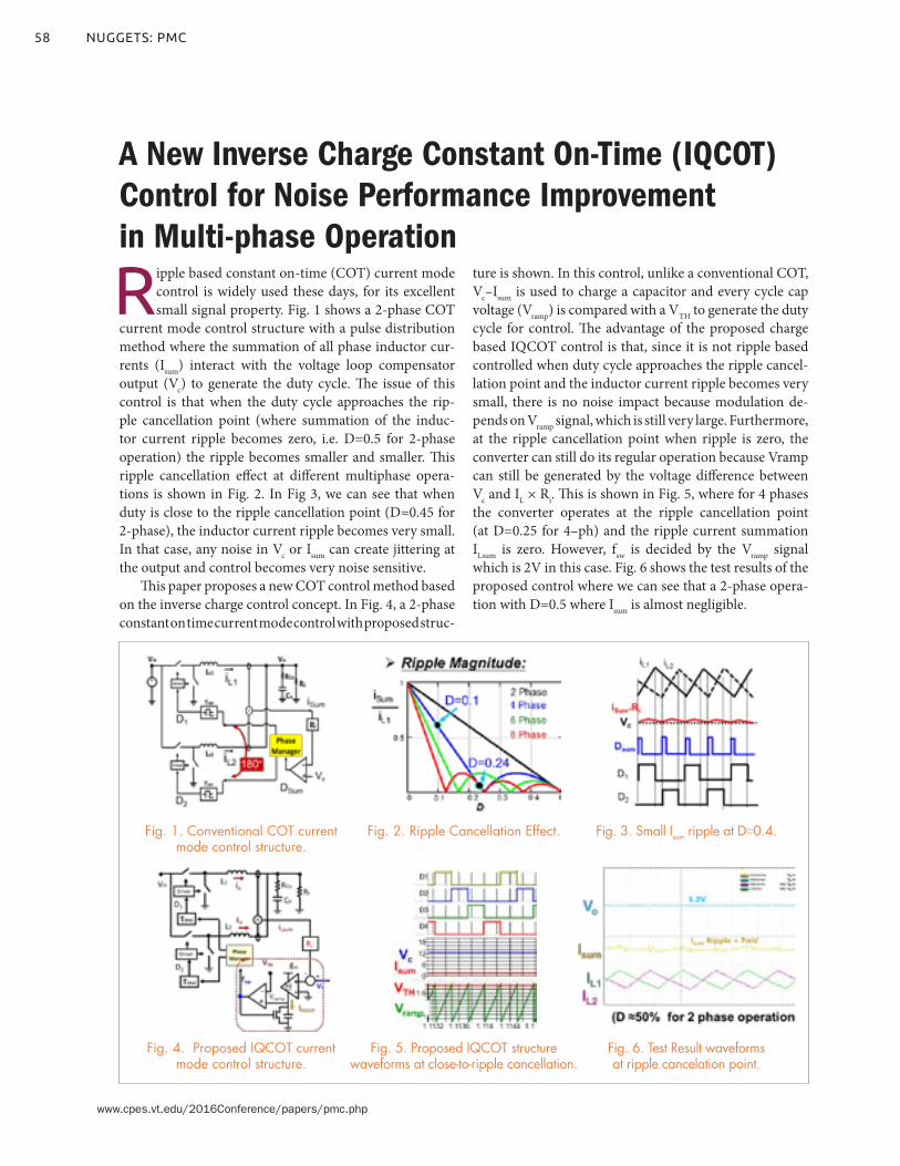
58
www.cpes.vt.edu/2016Conference/papers/pmc.php
NUGGETS: PMC
A New Inverse Charge Constant On-Time (IQCOT) Control for Noise Performance Improvement in Multi-phase Operation
Ripple based constant on-time (COT) current mode control is widely used these days, for its excellent small signal property. Fig. 1 shows a 2-phase COT
current mode control structure with a pulse distribution method where the summation of all phase inductor cur-rents (Isum) interact with the voltage loop compensator output (Vc) to generate the duty cycle. The issue of this control is that when the duty cycle approaches the rip-ple cancellation point (where summation of the induc-tor current ripple becomes zero, i.e. D=0.5 for 2-phase operation) the ripple becomes smaller and smaller. This ripple cancellation effect at different multiphase opera-tions is shown in Fig. 2. In Fig 3, we can see that when duty is close to the ripple cancellation point (D≈0.45 for 2-phase), the inductor current ripple becomes very small. In that case, any noise in Vc or Isum can create jittering at the output and control becomes very noise sensitive.
This paper proposes a new COT control method based on the inverse charge control concept. In Fig. 4, a 2-phase constant on time current mode control with proposed struc-
ture is shown. In this control, unlike a conventional COT, Vc–Isum is used to charge a capacitor and every cycle cap voltage (Vramp) is compared with a VTH to generate the duty cycle for control. The advantage of the proposed charge based IQCOT control is that, since it is not ripple based controlled when duty cycle approaches the ripple cancel-lation point and the inductor current ripple becomes very small, there is no noise impact because modulation de-pends on Vramp signal, which is still very large. Furthermore, at the ripple cancellation point when ripple is zero, the converter can still do its regular operation because Vramp can still be generated by the voltage difference between Vc and IL × Ri. This is shown in Fig. 5, where for 4 phases the converter operates at the ripple cancellation point (at D=0.25 for 4–ph) and the ripple current summation ILsum is zero. However, fsw is decided by the Vramp signal which is 2V in this case. Fig. 6 shows the test results of the proposed control where we can see that a 2-phase opera-tion with D=0.5 where Isum is almost negligible.
Fig. 1. Conventional COT current mode control structure.
Fig. 4. Proposed IQCOT current mode control structure.
Fig. 2. Ripple Cancellation Effect.
Fig. 5. Proposed IQCOT structure waveforms at close-to-ripple cancellation.
Fig. 3. Small Isum ripple at D≈0.4.
Fig. 6. Test Result waveforms at ripple cancelation point.
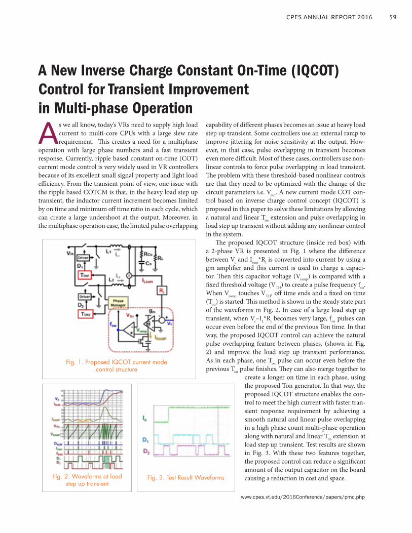
59CPES ANNUAL REPORT 2016
www.cpes.vt.edu/2016Conference/papers/pmc.php
A New Inverse Charge Constant On-Time (IQCOT) Control for Transient Improvement in Multi-phase Operation
As we all know, today’s VRs need to supply high load current to multi-core CPUs with a large slew rate requirement. This creates a need for a multiphase
operation with large phase numbers and a fast transient response. Currently, ripple based constant on-time (COT) current mode control is very widely used in VR controllers because of its excellent small signal property and light load efficiency. From the transient point of view, one issue with the ripple based COTCM is that, in the heavy load step up transient, the inductor current increment becomes limited by on time and minimum off time ratio in each cycle, which can create a large undershoot at the output. Moreover, in the multiphase operation case, the limited pulse overlapping
capability of different phases becomes an issue at heavy load step up transient. Some controllers use an external ramp to improve jittering for noise sensitivity at the output. How-ever, in that case, pulse overlapping in transient becomes even more difficult. Most of these cases, controllers use non-linear controls to force pulse overlapping in load transient. The problem with these threshold-based nonlinear controls are that they need to be optimized with the change of the circuit parameters i.e. Vout. A new current mode COT con-trol based on inverse charge control concept (IQCOT) is proposed in this paper to solve these limitations by allowing a natural and linear Ton extension and pulse overlapping in load step up transient without adding any nonlinear control in the system.
The proposed IQCOT structure (inside red box) with a 2-phase VR is presented in Fig. 1 where the difference between Vc and Isum*Ri is converted into current by using a gm amplifier and this current is used to charge a capaci-tor. Then this capacitor voltage (Vramp) is compared with a fixed threshold voltage (VTH) to create a pulse frequency fsw. When Vramp touches VTH, off time ends and a fixed on time (Ton) is started. This method is shown in the steady state part of the waveforms in Fig. 2. In case of a large load step up transient, when Vc–IL*Ri becomes very large, fsw pulses can occur even before the end of the previous Ton time. In that way, the proposed IQCOT control can achieve the natural pulse overlapping feature between phases, (shown in Fig. 2) and improve the load step up transient performance. As in each phase, one Ton pulse can occur even before the previous Ton pulse finishes. They can also merge together to
create a longer on time in each phase, using the proposed Ton generator. In that way, the proposed IQCOT structure enables the con-trol to meet the high current with faster tran-sient response requirement by achieving a smooth natural and linear pulse overlapping in a high phase count multi-phase operation along with natural and linear Ton extension at load step up transient. Test results are shown in Fig. 3. With these two features together, the proposed control can reduce a significant amount of the output capacitor on the board causing a reduction in cost and space.
Fig. 1. Proposed IQCOT current mode control structure
Fig. 2. Waveforms at load step up transient
Fig. 3. Test Result Waveforms

60
www.cpes.vt.edu/2016Conference/papers/pmc.php
NUGGETS: PMC
A New Inverse Charge Constant On-time (IQCOT) Control with Ultrafast Load Transient Response
Ripple based current-mode constant on-time (COT) control is currently widely used in VR controllers for its excellent small signal property and light load effi-
ciency. One issue concerning this ripple-based COT control is that in the heavy load step up transient, the inductor cur-rent increment becomes limited by the fixed on time and sys-tem minimum off time ratio in each cycle, which can create a large undershoot at the output. On the other hand, in the load step down case, if a load change occurs at the begin-ning of fixed Ton, the inductor current keeps increasing un-til the end of Ton, instead of decreasing. In that case, a large overshoot can occur at the output as well. Some controllers use nonlinear controls to increase or decrease the Ton at load transient. Threshold based nonlinear controls are problem-atic because they need to be optimized with the change of the circuit parameters, i.e. Vout, to avoid overcorrection or ring back at the output. This optimization process makes the sys-tem more complex. A new current mode COT control based on inverse charge control concept IQCOT is proposed to solve these limitations by allowing for a natural and linear Ton
extension in the load step up transient and to truncate the Ton in load step down transient, without adding any nonlinear control in the system.
The proposed IQCOT structure is presented in Fig. 1 where the difference between Vc and IL*Ri is converted into current by using a gm amplifier and this current is used to charge a capacitor. Then this capacitor voltage (Vramp) is com-pared with a fixed threshold voltage (VTH) to create pulse frequency fsw. When Vramp touches VTH, off time ends and a fixed on time (Ton) is started. In case of a large load step up transient, when Vc-IL*Ri becomes very large, fsw pulses can oc-cur even before the end of previous on time. If these very close pulses are allowed to merge to create a longer on time (Fig. 2), a significant undershoot reduction can be done at the output. Figs. 4 and 5 show that the Vout undershoot can be reduced by naturally increasing the Ton using the pulse merg-ing feature of the proposed control. Another important fea-ture is, as the fsw pulse increment is proportional to Vc-IL*Ri (Fig. 2), the Ton extension is eventually linearly proportional to the Vout undershoot. This will eliminate any chance of
overcorrection or ring-back of Vout which is a major problem in a fixed Ton extension method by nonlinear controls. Fig 3 shows that when an overshoot is created in Vout at load step down, Vc goes down very quickly and cross the IL*Ri which can be used to create a logic (like Vos in Fig. 3) and use it to truncate the constant Ton immediate-ly in order to reduce the Vout overshoot (as shown in Fig. 6).
Fig. 1. Proposed IQCOT current mode control structure.
Fig. 4. Conventional COT with no pulse merging.
Fig. 2. Waveforms at load step up transient.
Fig. 5. Proposed IQCOT with pulse merging.
Fig. 3 Waveforms at load step down transient.
Fig. 6. Overshoot reduction at load step up using proposed control.

61CPES ANNUAL REPORT 2016
www.cpes.vt.edu/2016Conference/papers/pmc.php
Variable Slope External Ramp to Improve the Transient Performance in Constant On-Time Current Mode Control
Constant on-time current mode (COTCM) con-trol schemes are widely used in the industry for their light load efficiency, higher BW design with
simpler compensation requirement and better transient performances. In a COTCM multiphase operation, the summation of all phase inductor current (Isum) interacts with a voltage loop compensator output (Vc) to generate the duty cycle. The issue with this method is that when duty cycle approaches the ‘ripple cancellation point’ (e.g. D=0.5 for 2-ph operation) this inductor current sum-mation (Isum) becomes increasingly smaller. In that case, control becomes very noise sensitive and output shows jittering. Normally, an external ramp (Se) is added to the modulator to reduce this jittering. But, unfortunately, with the increment of the external ramp value, although the jitter in the system gets reduced, the transient perfor-mance becomes worse. Moreover, the system bandwidth also decreases with the increment of external ramp, which eventually slows down the transient response even more. For these reasons, from a transient point of view, it is very challenging to use a large external ramp in the system to reduce jittering. In this paper, a novel method is proposed to modify the external ramp at the transient instant to improve the transient response (by increasing the slope of the ramp), and thus allow the control to use the large external ramp for noise per-formance improvement and enjoy the fast transient response at the same time.
In Fig 1, the proposed structure where the derivative of Vc to increase the ramp slope in transient, is added with the con-ventional COTCM structure. In conven-tional COTCM in Fig. 2 (a), we can see that with the large external ramp, the Vc and Isum distance is very large in the steady state. Therefore, at the load transient it becomes very difficult for Vc and Isum to cross each other, which prohibits the duty cycle from saturating in order to increase the inductor current quickly. In Fig. 2(a), we can see that when a heavy load transient occurs, the
dVc/dt is added with the slope of the ex-ternal ramp, which is shown by a green circle in Fig. 2(b). As the slope becomes very high at tran-sient, the duty cycle also becomes very high very quickly in order to increase the inductor current, which reduces un-dershoot at output. Comparing Fig. 2(a) and 2(b), we can clearly see that output voltage under-shoot can be reduced by using the proposed method. The main advantages of this method are, since we have used dv/dt of Vc, the detection is fast and optimum, which will reduce any chance of ring back. In this method, there is no threshold detection and the small signal property is not affected by the proposed method. By using the proposed method, COTCM control can have both a high noise per-formance and a fast transient performance together.
Fig. 1. Proposed variable ramp COTCM structure by adding dVc/dt with conventional ext. ramp.
Fig. 2 (a). Transient response of COTCM with fixed ramp (b). Transient response of COTCM with proposed variable ramp
at transient.
(a) (b)
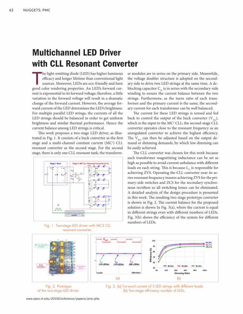
62
www.cpes.vt.edu/2016Conference/papers/pmc.php
NUGGETS: PMC
Multichannel LED Driver with CLL Resonant Converter
The light-emitting diode (LED) has higher luminous efficacy and longer lifetime than conventional light sources. Moreover, LEDs are eco-friendly and have
good color rendering properties. An LED’s forward cur-rent is exponential to its forward voltage; therefore, a little variation in the forward voltage will result in a dramatic change of the forward current. However, the average for-ward current of the LED determines the LED’s brightness. For multiple parallel LED strings, the currents of all the LED strings should be balanced in order to get uniform brightness and similar thermal performance. Hence the current balance among LED strings is critical.
This work proposes a two-stage LED driver, as illus-trated in Fig. 1. It consists of a buck converter as the first stage and a multi-channel constant current (MC3) CLL resonant converter as the second stage. For the second stage, there is only one CLL resonant tank; the transform-
er modules are in series on the primary side. Meanwhile, the voltage doubler structure is adopted on the second-ary side to drive two LED strings at the same time. A dc-blocking capacitor Cdc is in series with the secondary-side winding to ensure the current balance between the two strings. Furthermore, as the turns ratio of each trans-former and the primary current is the same, the second-ary current for each transformer can be well balanced.
The current for these LED strings is sensed and fed back to control the output of the buck converter (Vbus), which is the input to the MC3 CLL; the second-stage CLL converter operates close to the resonant frequency as an unregulated converter to achieve the highest efficiency. The VBus can then be adjusted based on the output de-mand or dimming demands, by which low dimming can be easily achieved.
The CLL converter was chosen for this work because each transformer magnetizing inductance can be set as high as possible to avoid current unbalance with different loads on each string. This is because Lr1 is responsible for achieving ZVS. Operating the CLL converter near its se-ries resonant frequency insures achieving ZVS for the pri-mary-side switches and ZCS for the secondary synchro-nous rectifiers so all switching losses can be eliminated. A detailed analysis of the design procedure is presented in this work. The resulting two-stage prototype converter is shown in Fig. 2. The current balance for the proposed solution is shown In Fig. 3(a), where the current is equal in different strings even with different numbers of LEDs. Fig. 3(b) shows the efficiency of the system for different numbers of LEDs.
Fig. 2. Prototype of the two-stage LED driver.
Fig. 3. (a) Forward current of 3 LED strings with different loads (b) Two-stage efficiency number of LEDs.
Fig. 1. Two-stage LED driver with MC3 CLL resonant converter.
(a) (b)

63CPES ANNUAL REPORT 2016
www.cpes.vt.edu/2016Conference/papers/pmc.php
Avoiding Divergent Oscillation of a Cascode GaN Device under High Current Turn-off Condition
In the cascode configuration shown in Fig. 1, junction capacitances of the two devices play an important role in the dynamic performance of the cascode device.
Capacitance mismatch between the high voltage GaN and the low voltage Si MOSFET may induce several un-desired features, such as when the Si MOSFET reaches avalanche during the turn-off transition in every switch-ing cycle, and the high-voltage GaN switch loses zero-voltage switching (ZVS) turn-on internally even when a ZVS technique is applied.
This paper presents another issue related to the ca-pacitance mismatch in the cascode GaN devices that would cause device and circuit failure. The parasitic ring-ing during the turn-off transition may trigger the GaN device to internally turn on at the high current turn off condition. The parasitic resonant impedance network changes when GaN is turned on and it absorbs more en-ergy from the source. The resonant amplitude gradually increases and becomes divergent oscillation. This phe-nomenon may result in failure for the cascode GaN de-vice and other circuit components.
One way to avoid the diver-gent oscillation is to parallel a RC snubber circuit which dissipates higher energy and is not suit-able for high-frequency opera-tion. A fundamental solution to this issue is to add an additional capacitor CX, as shown in Fig. 1. Considering all the parasitic in-ductance induced by adding CX, the position of CX is critical to achieving optimal performance. Two possible packaging diagrams for integrating CX are shown in Fig. 2, and both are analyzed in detail in this paper. Packaging B has a much better performance. Experimental verification results are shown in Fig. 3. The proposed method extends the high current turn-off capability and improves device performance significantly.
Fig. 1. Fundamental solution to solve capacitance mismatch issue.
Fig. 2. Two possible packaging diagrams for integrating CX.
Fig. 3. Experimental verification results.
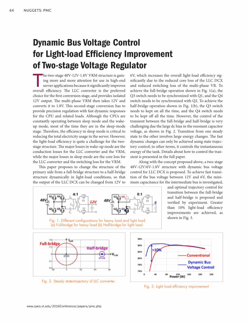
64
www.cpes.vt.edu/2016Conference/papers/pmc.php
NUGGETS: PMC
Dynamic Bus Voltage Control for Light-load Efficiency Improvement of Two-stage Voltage Regulator
The two-stage 48V-12V-1.8V VRM structure is gain-ing more and more attention for use in high-end server applications because it significantly improves
overall efficiency. The LLC converter is the preferred choice for the first conversion stage, and provides isolated 12V output. The multi-phase VRM then takes 12V and converts it to 1.8V. This second-stage conversion has to provide precision regulation with fast dynamic responses for the CPU and related loads. Although the CPUs are constantly operating between sleep mode and the wake-up mode, most of the time they are in the sleep-mode stage. Therefore, the efficiency in sleep mode is critical to reducing the total electricity usage in the server. However, the light-load efficiency is quite a challenge for the two-stage structure. The major losses in wake-up mode are the conduction losses for the LLC converter and the VRM, while the major losses in sleep mode are the core loss for the LLC converter and the switching loss for the VRM.
This paper proposes to change the structure of the primary side from a full-bridge structure to a half-bridge structure dynamically in light-load conditions, so that the output of the LLC DCX can be changed from 12V to
6V, which increases the overall light-load efficiency sig-nificantly due to the reduced core loss of the LLC DCX and reduced switching loss of the multi-phase VR. To achieve the full-bridge operation shown in Fig. 1(a), the Q3 switch needs to be synchronized with Q1, and the Q4 switch needs to be synchronized with Q2. To achieve the half-bridge operation shown in Fig. 1(b), the Q3 switch needs to kept on all the time, and the Q4 switch needs to be kept off all the time. However, the control of the transient between the full-bridge and half-bridge is very challenging due the large dc bias in the resonant capacitor voltage, as shown in Fig. 2. Transition from one steady state to the other involves large energy changes. The fast dynamic changes can only be achieved using state trajec-tory control; in other terms, it controls the instantaneous energy of the tank. Details about how to control the tran-sient is presented in the full paper.
Along with the concept proposed above, a two-stage 48V-12V/6V-1.8V structure with dynamic bus voltage control for LLC DCX is proposed. To achieve fast transi-tion of the bus voltage between 12V and 6V, the mini-mum capacitance for the intermediate bus is investigated,
and optimal trajectory control for transition between the full-bridge and half-bridge is proposed and verified by experiment. Greater than 10% light-load efficiency improvements are achieved, as shown in Fig. 3.
Fig. 2. Steady state-trajectory of LLC converter.Fig. 3. Light load efficiency improvement
Fig. 1. Different configurations for heavy load and light load (a) Full-bridge for heavy load (b) Half-bridge for light load.

65CPES ANNUAL REPORT 2016
www.cpes.vt.edu/2016Conference/papers/pmc.php
Omnidirectional Wireless Power Transfer for Portable Devices
Recently, the wireless power transfer product market has been increasing rapidly due to the convenience of charging devices wirelessly. Low-power devices,
such as consumer electronics and mobile devices, share a large portion of this large and growing market. However, the majority of wireless power transfer platforms in the current market are directional, which means devices can only be charged efficiently in one orientation. For exam-ple, a smart phone cannot be charged quickly in a planar charging surface when it is vertical to the surface. There-fore, an omnidirectional wireless power transfer platform is highly desirable.
In this paper, a numerical model and a simulation platform are built to evaluate the flux direction of omnidi-rectional wireless power transfer systems. The omnidirec-tional wireless power transfer platforms proposed by Intel and City University of Hong Kong are state-of-the-art solutions. With numerical model and FEA simula-tion tools, the flux direction of these two state-of-the-art platforms are evaluated. Unfortunately, there is no omnidirectional flux in the bottom of the two charging platforms.
The flux direction preference for portable devices is shown in Figure 1(a). For mechanical reasons, a small portable device will drop into the bottom of charging platform. Since
the orientation is very flexible for small portable devices, omnidirectional flux direction is preferred in the bottom. On the other hand, a planar device can only lay on its side face. Therefore, flux perpendicular to the surface is pre-ferred for planar devices. A new transmitter coil structure to achieve omnidirectional flux in the bottom and per-pendicular flux on the side face is proposed, as shown in Figure 1(b). With this new coil structure, the device can be simply dropped to the platform and charged efficiently.
For the proposed transmitter coil structure, it’s easy to understand flux is perpendicular to the side face. On the other hand, the omnidirectional flux distribution in the bottom of the proposed transmitter coil structure can be verified by simulation and the numerical model. Figure 2 shows the flux distribution in the bottom at different times.
Fig. 2. Flux distribution in bottom of charging platform at different times.
Fig. 1. Omnidirectional WPT platform.
(a). Flux direction preference (b). Transmitted coil structure
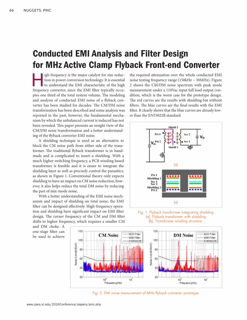
66
www.cpes.vt.edu/2016Conference/papers/pmc.php
NUGGETS: PMC
Conducted EMI Analysis and Filter Design for MHz Active Clamp Flyback Front-end Converter
High frequency is the major catalyst for size reduc-tion in power conversion technology. It is essential to understand the EMI characteristic of the high
frequency converter, since the EMI filter typically occu-pies one third of the total system volume. The modeling and analysis of conducted EMI noise of a flyback con-verter has been studied for decades. The CM/DM noise transformation has been described and some analysis was reported in the past, however, the fundamental mecha-nism by which the unbalanced current is induced has not been revealed. This paper presents an insight view of the CM/DM noise transformation and a better understand-ing of the flyback converter EMI noise.
A shielding technique is used as an alternative to block the CM noise path from either side of the trans-former. The traditional flyback transformer is in hand-made and is complicated to insert a shielding. With a much higher switching frequency, a PCB winding based transformer is feasible and it is easier to integrate the shielding layer as well as precisely control the parasitics, as shown in Figure 1. Conventional theory only expects shielding to have an impact on CM noise reduction, how-ever, it also helps reduce the total DM noise by reducing the part of mix-mode noise.
With a better understanding of the EMI noise mech-anism and impact of shielding on total noise, the EMI filter can be designed effectively. High-frequency opera-tion and shielding have significant impact on EMI filter design. The corner frequency of the CM and DM filter shifts to higher frequency, which requires a smaller CM and DM choke. A one-stage filter can be used to achieve
the required attenuation over the whole conducted EMI noise testing frequency range (150kHz ~ 30MHz). Figure 2 shows the CM/DM noise spectrum with peak mode measurement under a 110Vac input full load output con-dition, which is the worst case for the prototype design. The red curves are the results with shielding but without filters. The blue curves are the final results with the EMI filter. It clearly shows that the blue curves are already low-er than the EN55022B standard.
Fig. 1. Flyback transformer integrating shielding (a). Flyback transformer with shielding
(b). Transformer winding structure.
(a)
(a)
Fig. 2. EMI noise measurement of MHz flyback converter prototype.

67CPES ANNUAL REPORT 2016
www.cpes.vt.edu/2016Conference/papers/pmc.php
Design Consideration of MHz Active Clamp Flyback Converter with GaN Devices for Low Power Adapter Application
One of the biggest market of power supplies, in both volume and revenue, is the ac-dc adapter/charger for consumer electronics. The market is
projected to surpass $8 billion in 2015 and reach $9 bil-lion by 2018; with much of this growth driven by smart phones, tablets and a number of emerging applications. The adapter is strongly driven by efficiency and power density for all forms of portable electronics. Most adapt-ers only operate at relatively low frequencies (<100 kHz), with state-of-the-art efficiency up to 91.5%. However, low-frequency operation limits the adapter power den-sity to 6-9 W/in3. The emerging GaN device is deemed a game-changing device in this particular application, with improved efficiency and significant size reduction.
Flyback converters are the dominant topology for low-power adapter applications due to their simplicity and low cost. With an active clamp circuit, the leakage en-ergy can be recycled, and the voltage ringing minimized. Moreover, ZVS for both the main switch and the clamp-ing switch can be realized by proper design as well. The traditional flyback transformer is hand-made, which is an intensive, labor-involved manufacturing process. The manufacturing cost is a concern, and the parameter varia-tion is another circuit design issue. A PCB winding-based
transformer is only feasible when the switching frequency is over several hundred kHz due to its capacity for fewer turns and a smaller core size. The leakage inductance and parasitic capacitance of the transformer can be well-con-trolled by PCB manufacturers. Moreover, shielding can be easily integrated in the PCB winding to reduce the CM noise.
Fig. 1 shows the prototype of a MHz active clamp fly-back front-end converter. The size of the flyback trans-former, EMI filter and output filter are significantly re-duced, with 10 times higher switching frequency than current industry practice. The power density excluding the case is over 40W/in3, which is two times higher than the state-of-the-art product. The measured full load ef-ficiency over a wide input range is shown in Figure 2. The efficiency of the prototype is 1–2% higher than the state-of-the-art product. It is worthwhile to point out that the power density improvement is accompanied with ef-ficiency improvement due to thermal restriction. Based on the thermal simulation carried on a converter which is enclosed by a case, the converter efficiency should be above 92% at worst case to achieve 25W/in3 power density without violating the thermal standard IEC60950.
Fig. 1. Prototype of 1MHz 65W active clamp flyback converter.
Fig. 2. Comparison of Efficiency.
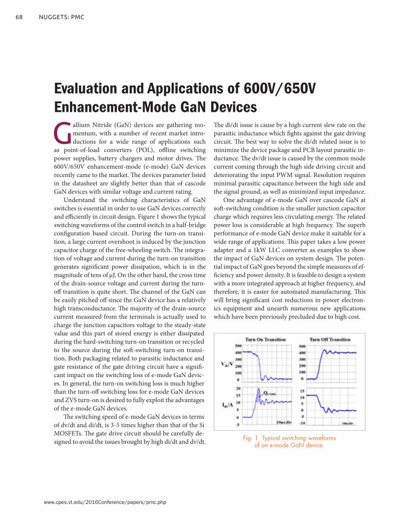
68
www.cpes.vt.edu/2016Conference/papers/pmc.php
NUGGETS: PMC
Evaluation and Applications of 600V/650V Enhancement-Mode GaN Devices
Gallium Nitride (GaN) devices are gathering mo-mentum, with a number of recent market intro-ductions for a wide range of applications such
as point-of-load converters (POL), offline switching power supplies, battery chargers and motor drives. The 600V/650V enhancement-mode (e-mode) GaN devices recently came to the market. The devices parameter listed in the datasheet are slightly better than that of cascode GaN devices with similar voltage and current rating.
Understand the switching characteristics of GaN switches is essential in order to use GaN devices correctly and efficiently in circuit design. Figure 1 shows the typical switching waveforms of the control switch in a half-bridge configuration based circuit. During the turn-on transi-tion, a large current overshoot is induced by the junction capacitor charge of the free-wheeling switch. The integra-tion of voltage and current during the turn-on transition generates significant power dissipation, which is in the magnitude of tens of μJ. On the other hand, the cross time of the drain-source voltage and current during the turn-off transition is quite short. The channel of the GaN can be easily pitched off since the GaN device has a relatively high transconductance. The majority of the drain-source current measured from the terminals is actually used to charge the junction capacitors voltage to the steady-state value and this part of stored energy is either dissipated during the hard-switching turn-on transition or recycled to the source during the soft-switching turn-on transi-tion. Both packaging related to parasitic inductance and gate resistance of the gate driving circuit have a signifi-cant impact on the switching loss of e-mode GaN devic-es. In general, the turn-on switching loss is much higher than the turn-off switching loss for e-mode GaN devices and ZVS turn-on is desired to fully exploit the advantages of the e-mode GaN devices.
The switching speed of e-mode GaN devices in terms of dv/dt and di/dt, is 3-5 times higher than that of the Si MOSFETs. The gate drive circuit should be carefully de-signed to avoid the issues brought by high di/dt and dv/dt.
The di/dt issue is cause by a high current slew rate on the parasitic inductance which fights against the gate driving circuit. The best way to solve the di/dt related issue is to minimize the device package and PCB layout parasitic in-ductance. The dv/dt issue is caused by the common mode current coming through the high side driving circuit and deteriorating the input PWM signal. Resolution requires minimal parasitic capacitance between the high side and the signal ground, as well as minimized input impedance.
One advantage of e-mode GaN over cascode GaN at soft-switching condition is the smaller junction capacitor charge which requires less circulating energy. The related power loss is considerable at high frequency. The superb performance of e-mode GaN device make it suitable for a wide range of applications. This paper takes a low power adapter and a 1kW LLC converter as examples to show the impact of GaN devices on system design. The poten-tial impact of GaN goes beyond the simple measures of ef-ficiency and power density. It is feasible to design a system with a more integrated approach at higher frequency, and therefore, it is easier for automated manufacturing. This will bring significant cost reductions in power electron-ics equipment and unearth numerous new applications which have been previously precluded due to high cost.
Fig. 1. Typical switching waveforms of an e-mode GaN device.

69CPES ANNUAL REPORT 2016
www.cpes.vt.edu/2016Conference/papers/pmc.php
Digital Controlled MHz Critical Mode PFC with Simplified On-time Calculation for Minimizing Input Current Distortion
In order to implement critical conduction mode (CRM) control for a GaN-based MHz totem-pole PFC with a commercial low-cost microcontroller (MCU), a simple,
but very accurate, on-time calculation method is pro-posed for implementing programmed on-time control at high frequency and achieving a low current THD.
On-time calculation was previously based on the state-plane trajectory shown in Fig. 1. From Fig. 1, an analytical model of the inductor current is derived to calculate the average inductor current. To achieve a low current THD, the average inductor current needs to follow a sinusoidal shape. By making the average inductor current equal to the sinusoidal reference current, an on-time distribution in line-cycle is derived as a highly non-linear complicated expression. The calculation time is estimated to be more than 3000 CPU cycles of MCU, for 120MHz MCU, which is equivalent to several tens of switching periods at MHz frequency level. This long calculation time makes on-time update slowly and causes a high current THD.
So here, a triangular-shape approximation is made on the switching-cycle inductor current waveform, as the black dash line shown in Fig. 2, since the nonlinear part of the waveform only happens during resonance, which is a much shorter time period compared to the switching pe-riod. The approximation simplifies the calculation of the average inductor current, which is simply the average of peak current and valley current.
Similarly, by making the average inductor current equal to the sinusoidal reference current, on-time distri-bution in line-cycle is derived as a very simple expression.
After simplification, the required calculation time is about 30 CPU cycles of MCU, for 120MHz MCU, equiv-alent to a quarter of the switching period even at MHz high frequency, which demonstrates a more than 100x improvement. As shown in Fig. 3, accuracy is not sacri-ficed due to the simplification, and what’s more, low cur-rent THD is achieved.
Fig. 1. State-plane trajectory.
Fig. 3. Comparison of two calculation methods in (a) on-time distribution (b) THD simulation result.
Fig. 2. Approximation in inductor current.
(a) (b)

70
www.cpes.vt.edu/2016Conference/papers/pmc.php
NUGGETS: PMC
Microcontroller-based Critical Mode Control with Improved Zero-Current-Detection for MHz Totem-pole PFC
In order to implement critical conduction mode (CRM) control for a GaN-based MHz totem-pole PFC with a commercial low-cost microcontroller (MCU), a novel
but very simple zero-current-detection (ZCD) method is proposed to solve a signal processing delay related issue, which is significant at MHz high frequency.
Previously, the inductor current positive-to-negative zero-crossing is sensed to trigger SR turn-off. However, a signal processing delay in the MCU and gate driver makes the SR turn off later, which causes a significant unwanted negative current at MHz high frequency. The unwanted negative current leads to an increase of current ripple, conduction loss and EMI filter size.
In this paper, an inductor current positive-to-nega-tive zero-crossing is used for triggering control switch turn-off. Ideally, the interval between the zero-crossing instant and the control switch turn-off instant is the on-time, Ton, which means after zero-crossing is sensed, de-lay by Ton, and then turn off control switch. Considering the signal processing delay, since the on-time is typically greater than this delay, compensation is easily made by subtracting this delay from Ton to get the actual time delay from the sensed zero-crossing instant to control switch
turn-off instant, which the MCU needs to know, as shown in Fig. 1.
Also for the MCU, the actual time delay for SR turn-off and for control switch turn-on are shown as TSR_delay and Tdelay in Fig. 1.
With this improved ZCD method, the inductor cur-rent waveform in half line-cycle is shown in Fig. 2. The unwanted negative current, and its impact on conduction loss and on EMI filter size are eliminated.
Fig. 1. Waveform with the improved CRM control method.
Fig. 2. Line-cycle inductor current simulation waveform (a) without improved ZCD (b) with improved ZCD.
(a) (b)

71CPES ANNUAL REPORT 2016
www.cpes.vt.edu/2016Conference/papers/pmc.php
State-Trajectory Control with Single-Cycle Response for POL Converters
For dc-dc converters, variable-frequency controls are widely used to improve the light-load efficiency, increase transient-response speed, and reduce the
amount of output capacitors by utilizing high-band-width designs. One popular variable-frequency control is the Constant On-Time control (COT). COT control achieves variable frequency by utilizing a fixed on-time (Ton). As the input and output of the system varies during operation, the frequency changes automatically to meet the load demand. However, the response speed when transient occurs is limited by the fixed Ton and multiple cycles are needed to achieve the new steady-state.
The fastest transient response is a single-cycle re-sponse. The proposed COT with single-cycle transient improvement is shown in detail in Fig. 1. The trajec-tory of the conventional COT is shown in Fig. 2 in red, and the trajectory of the proposed control is in purple. The control law of COT is given as iLRi=Vc. Assuming the compensator Hv is pure gain, K, the control law can be drawn on the trajectory as shown in Fig. 2. During steady-state, the operation of COT is always to the right of the control law. When a load step-up transient occurs at t0, the state-trajectory changes and drifts to the left of the control law at t1. For conventional COT shown in red, due to the fixed Ton, the trajectory turns off at t2 and fol-lows a multi-cycle response until the system recovers to steady-state COT operation, to the right of the control law. For single-cycle response, when the state-trajectory drifts to the left of the control law at t1, it follows the nat-ural trajectory until the system recovers to steady-state COT operation. Comparing the two trajectories, the tra-jectory control with single-cycle response (purple) has the fastest and most direct path to the new steady-state.
Experimental results for the proposed state-trajecto-ry control with single-cycle response for COT is obtained by making external modifications to the TPS5960 evalu-ation board by Texas Instruments after three 470uF bulk output capacitors are removed. For single-phase opera-tion with Vin=12V, Vref=1.2V, and using the on-board 32A dynamic load, the performance of COT with single-cycle modifications is shown in Fig. 3. After the load step-up transient is detected, COT with single-cycle is able to go from one steady-state to another steady-state much faster than the conventional COT.
Fig. 1. COT with single-cycle transient improvement in yellow.
Fig. 3. Experimental results of COT with single-cycle response.
Fig. 2. Trajectory of conventional COT (red) vs Trajectory Control with Single-Cycle Response (purple).

72
www.cpes.vt.edu/2016Conference/papers/pmc.php
NUGGETS: PMC
Improved Constant On-Time Control with Single-Cycle Load Transient for Multiphase Voltage Regulator
For dc-dc converters, variable-frequency controls are widely used to improve the light-load efficiency, increase transient-response speed, and reduce the
amount of output capacitors by utilizing high-bandwidth designs. One popular variable-frequency current-mode control is the Constant On-Time control (COT). COT control achieves variable frequency by utilizing a fixed on-time (Ton). As the input and output of the system var-ies during operation, the frequency changes automati-cally to meet the load demand. However, the transient response speed of COT is slow due to fixed Ton.
The fastest transient response is a single-cycle re-sponse. The proposed COT with single-cycle transient improvement is shown in Fig. 1 and its operation during transient is shown in Fig. 2. By observing the Vcom signal, the beginning and end of transient necessary for a sin-gle-cycle response can be obtained. Vcom is the difference between Vc and iLRi; at steady-state. It operates within a steady-state band where the amplitude is determined by the inductor current ripple and the maximum is de-termined by a dc offset, Vth. During transient when the inductor is unable to follow the change in the load, Vcom naturally increases higher than Vth. As such, the begin-ning of transient can be detected using a threshold, Vup, placed slightly higher than Vth. Once transient is detected,
Ton is extended by modifying the Ton turn-off mechanism such that it is not triggered during transient. This is ac-complished by increasing Vth to a maximum voltage, Vmax, so Sr does not intersect with the voltage threshold during transient. When Vcom recovers to Vcom_min, Vmax is reduced back to Vth. The reduction in voltage levels will intersect with Sr, terminating the extended Ton pulse. At this time, normal operation of COT returns.
This method can easily be extended to multiphase op-eration by using the interleaving necessary for the steady-state to slow down the transient response speed. The fast-
est way to transfer energy in multiphase is to have all the phases on, or overlap-ping, while each phase is operating in single-cycle response. The simulation result of 2-phase COT with single-cycle transient improvement is shown in Fig. 3. From Fig. 3, Ton extension and phase overlapping are achieved during tran-sient, while interleaving is maintained during the steady-state operation of COT.
Fig. 1. COT with single-cycle transient improvement.
Fig. 3. Simulation of 2-phase COT with single-cycle transient improvement.
Fig. 2. The operation of single-cycle response.
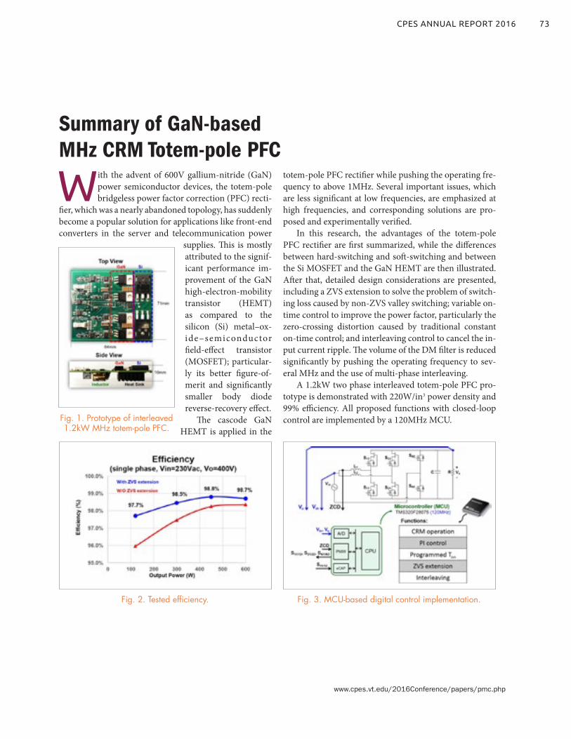
73CPES ANNUAL REPORT 2016
www.cpes.vt.edu/2016Conference/papers/pmc.php
Summary of GaN-based MHz CRM Totem-pole PFC
With the advent of 600V gallium-nitride (GaN) power semiconductor devices, the totem-pole bridgeless power factor correction (PFC) recti-
fier, which was a nearly abandoned topology, has suddenly become a popular solution for applications like front-end converters in the server and telecommunication power
supplies. This is mostly attributed to the signif-icant performance im-provement of the GaN high-electron-mobility transistor (HEMT) as compared to the silicon (Si) metal–ox-ide–semiconductor field-effect transistor (MOSFET); particular-ly its better figure-of-merit and significantly smaller body diode reverse-recovery effect.
The cascode GaN HEMT is applied in the
totem-pole PFC rectifier while pushing the operating fre-quency to above 1MHz. Several important issues, which are less significant at low frequencies, are emphasized at high frequencies, and corresponding solutions are pro-posed and experimentally verified.
In this research, the advantages of the totem-pole PFC rectifier are first summarized, while the differences between hard-switching and soft-switching and between the Si MOSFET and the GaN HEMT are then illustrated. After that, detailed design considerations are presented, including a ZVS extension to solve the problem of switch-ing loss caused by non-ZVS valley switching; variable on-time control to improve the power factor, particularly the zero-crossing distortion caused by traditional constant on-time control; and interleaving control to cancel the in-put current ripple. The volume of the DM filter is reduced significantly by pushing the operating frequency to sev-eral MHz and the use of multi-phase interleaving.
A 1.2kW two phase interleaved totem-pole PFC pro-totype is demonstrated with 220W/in3 power density and 99% efficiency. All proposed functions with closed-loop control are implemented by a 120MHz MCU. Fig. 1. Prototype of interleaved
1.2kW MHz totem-pole PFC.
Fig. 2. Tested efficiency. Fig. 3. MCU-based digital control implementation.
74
www.cpes.vt.edu/2016Conference/papers/pmc.php
NUGGETS: PMC
The totem-pole bridgeless power-factor-correction (PFC) circuit is becoming popular mainly because of the emerging high voltage gallium-nitride (GaN)
devices [1-6]. Soft switching operation is important in or-der to achieve a very high MHz frequency operation for 600V GaN devices. Critical conduction mode (CRM) is the simplest way to achieve soft switching; and when ap-plied to a boost-type PFC circuit, it is easy to achieve a good power factor with a CRM operation.
A 1.2kW 1-3MHz GaN-based CRM totem-pole PFC was built with close to 99% peak efficiency and more than 200W/in3 power density. In addition, the MHz impact of the PFC is not limiting but has an even more significant impact on the input filter design. According to a previ-ously published paper, when the switching frequency is higher, (e.g. above 400kHz), the smaller the filter size. We had demonstrations which show that from 100kHz to 1MHz, the DM filter is simplified from 2 stages to 1 stage and the volume is reduced by 50%. They also show that if a two-phase PFC is interleaved with a 180 degree phase shift then another 50% volume reduction is expected.
The challenge of interleaving control for a CRM PFC is the circuit variable frequency operation. For a given in-put and load condition, the frequency varies 3-5 times in a half line cycle. For different input or load conditions, the frequency range varies as well. According to previous literature, there are generally two categories of interleav-ing control methods proposed for the variable frequency CRM PFC: closed-loop interleaving and open-loop inter-leaving. For low frequency, both methods work well in maintaining a minimal value in the phase error. However, when the frequency is pushed 10 times higher to multi-MHz, the interleaving control becomes a new challenge.
In this research, the impact of interleaving control on a MHz CRM totem-pole PFC and DM filter is first in-troduced. The performance comparison between closed-loop interleaving and open-loop interleaving for MHz
totem-pole PFC is then discussed. The optimization and experimental results of open-loop interleaving are also presented. The conclusion shows that a less than 3 degree phase error is accomplished with open-loop interleaving and a 60MHz MCU. Finally, the stability analysis of open-loop interleaving is elaborated.
Digital-Based Interleaving Control for GaN-based MHz CRM Totem-pole PFC
Fig. 1. Circuit diagram of two-phase interleaved totem-pole PFC with cascode GaN devices.
Fig. 2. Experimental waveform of open-loop interleaving.

75CPES ANNUAL REPORT 2016
www.cpes.vt.edu/2016Conference/papers/pmc.php
The totem-pole bridgeless power factor correction (PFC) rectifier has a simpler topology and higher efficiency than other boost-type bridgeless PFC
rectifiers. Its promising performance is enabled by using high-voltage gallium nitride (GaN) high-electron-mo-bility transistors, with more benefits (e.g., lower reverse recovery charges and less switching losses) than the state-of-the-art silicon metal-oxide-semiconductor field-effect transistors. Cascode GaN devices in traditional packages, i.e., the TO-220 and power quad flat no-lead, are used in the totem-pole PFC boost rectifier but the parasitic in-ductances induced by the traditional packages not only significantly deteriorate the switching characteristics of the discrete GaN device but also adversely affect the performance of the built PFC rectifier. A new stack-die packaging structure with an embedded capacitor has been introduced and proven to be efficient in reducing parasitic ringing at the turn-off transition and achieving true zero-voltage-switching turn-on. However, the ther-mal dissipation capability of the device packaged in this configuration becomes a limitation on further pushing the operating frequency and the output current level for high-efficiency power conversion. This paper focuses on the thermal analysis of the cascode GaN devices in differ-ent packages and the GaN-based multichip module used in a two-phase totem-pole bridgeless PFC boost rectifier. A series of thermal models are built based on the actual structures and materials of the packaged devices to evalu-
ate their thermal performance. Finite element analysis (FEA) simulation results of the cascode GaN device in a flip-chip format demonstrate the possibility of increasing the device switching speed while maintaining the peak temperature of the device below 125° C. Thermal analysis of the GaN-based power module in a very similar struc-ture is also conducted using the FEA method. Experimen-tal data measured using the fabricated devices and mod-ules validate the simulation results. The developed new package in a flip-chip configuration enhances the thermal dissipation capability of the cascode GaN device in the stack-die format. The GaN-based power module built us-ing the same packaging structure also demonstrates desir-able thermal performance.
Thermal Analysis and Improvement of Cascode GaN Device Package for Totem-Pole Bridgeless PFC Rectifier
Fig. 1 The cross-sectional temperature distribution of the built thermal model for the stack-die packaged cascode
GaN device (Power loss = 8.8 W, Ta = 25° C).
Fig. 2. Thermal analysis for the GaN-based power module (Total power loss = 34 W, Ta = 20° C.

76
www.cpes.vt.edu/2016Conference/papers/pmc.php
NUGGETS: PMC
Recently V2 control has been widely applied in point-of-load buck converters. In contrast with the tradi-tional voltage or current mode, V2 control has the
following three features: 1) no current-sensing network is required; 2) fast load transient characteristics with direct output voltage feedback; and 3) the outer-loop compensator is much simpler. In this paper, an optimal design strategy is proposed after a thorough investigation of the small-signal model for constant frequency V2 control. The physical cau-sation of two pairs of double poles is identified and an ex-plicit stability criterion is presented. For the first time, it is found that different design strategies should be used with different capacitors. For OSCON capacitors, designing an external ramp is adequate, while for ceramic capacitors an additional current ramp is required to control the stability margin. This work mainly focuses on the constant frequen-cy V2 control, as shown in Fig.1.
First the case with no external ramp is considered, and the analysis shows that two kinds of sidebands can be decou-pled; inductor current sidebands cause one pair of double poles, and capacitor voltage sidebands cause another pair of double poles. To avoid the coupling and interacting of these sidebands, two factors should be considered; the duty ra-tio (D) and the current feedback strength (α). For different types of capacitors there are different stable regions that can be considered based on switching frequency, as shown in Fig. 2. With the addition of an external ramp, it was found that for the OSCON capacitor, the stability region can be extended to cover the whole duty cycle region with the ap-propriate selection of external ramp, as shown in Fig. 3.
For ceramic capaci-tors, the external ramp is not sufficient for stable op-eration. Therefore, a hybrid ramp strategy is proposed for the optimum design purposes; a current ramp is used to enhance the cur-rent strength feedback to minimize the effect of the capacitor voltage feedback loop, while an external ramp is used to reduce the sample and hold effect for
the inductor current feedback loop. Either inductor current or capacitor current can be used to enhance current feed-back strength for the ceramic capacitor case. As shown in Fig. 4, a well damped system can be achieved with a hybrid ramp.
The proposed hybrid ramp method was experimentally verified for the ceramic capacitor case, as shown in Fig. 5, where the analytical model agrees with the experimental results.
Small-Signal Analysis and Optimal Design of Constant Frequency V2 Control
Fig. 4. Control-to-output transfer function: (red) without hybrid ramp (blue) with hybrid
current ramp.
Fig. 1. Constant frequency V2 peak control (a) circuit diagram; (b) steadystate waveform.
Fig. 2. Stability criterion of constant frequency V2 peak
control with Fsw =300 kHz.
Fig. 3. Diagram of stability criterion with external ramp
compensation.
(a) (b)
Fig. 5. Experimental results for ceramic capacitors with hybrid ramp compensation. (a) Control-to-output voltage
transfer function (b) Load transient step-up.
(a) (b)
77CPES ANNUAL REPORT 2016
www.cpes.vt.edu/2016Conference/papers/pmc.php
Recently V2 control has become widely applied in point-of-load buck converters. In this paper, a unified equivalent circuit model for V2 control is proposed. The equivalent
circuit model has clear physical meaning and is very helpful for design. Fig. 1 explicitly shows three feedback paths of V2 control, and shows the frequency spectrum of each feedback path when the control signal is under modulation. Similar to current-mode control, the inductor current feedback does not have a low-pass filter, so all the sidebands are fed back to the modulator, and the sideband effect needs to be considered. The capacitor voltage loop is a direct feedback loop without any compensation. Therefore, the sidebands of the capacitor voltage also need to be taken into consideration. This complicates the scenario for finding an equivalent circuit model for V2 control.
The analysis shows that the buck converter with V2 control can be regarded as a non-ideal voltage source. The methodol-ogy used to derive an equivalent circuit model to represent this non-ideal voltage source is to establish the connection between V2 control and current-mode control; as the equivalent circuit model of current-mode control is well established, the result-ing equivalent circuit model is shown in Fig. 2. The non-ideal current source and non-ideal voltage source are virtually rep-resented by the resonance between Ls and Ce and Le and Co, re-spectively. The damping factor of the double poles caused by the capacitor voltage side-band is determined by the damping resistance Rdamp, depending on the capacitor parameters.
Due to the low ESR of ceramic capacitors, when they are used V2 has stability limitations to be applied. Several methods have been proposed to address this issue; one is using enhanced V2 constant on-time control by adding current ramp informa-tion; the other method where adaptive voltage positioning is undesired is using the enhanced V2 constant on-time control with a high-pass filter after current sensing; the third method is sensing the capacitor current. The complete equivalent cir-cuit model for these three methods is also derived in this work and shown in Fig. 3. A unified equivalent circuit model for V2
control is also proposed, as shown in Fig. 4; the model includes inductor current ramp Ri for all modulation schemes. Further-more, the model also includes external ramp compensation in constant frequency V2 control. The proposed equivalent circuit models are experimentally verified, as shown in Fig. 5.
Unified Equivalent Circuit Model and Optimal Design of V2-Controlled Buck Converters
Fig. 1. Frequency spectrum of direct feedback loop of V2 control with three feedback paths.
Fig. 2. Complete equivalent circuit model of constant on-time V2 control.
Fig. 4. Unified equivalent circuit model.
Fig. 5. Experimental verification of transfer functions.
Fig. 3. (a) Enhanced constant on time V2 control (b) With high pass filter
(c) With sensing capacitor current.
78
www.cpes.vt.edu/2016Conference/papers/pmc.php
NUGGETS: PMC
LLC resonant converters are widely used in industry. However, until now, no simple and accurate small-signal equivalent circuit model has been available.
This paper proposes a simple equivalent circuit model as a good design tool for LLC resonant converters. The simple equivalent circuit model is derived based on modification and simplification of an extended describing function method.
For LLC converter ZVS, the resonant tank behavior differs depending on the operating frequency. For Fs ≥ Fo, only Lr resonates with Cr, and Lm is clamped by the output voltage. For Fs < Fo, there is some time period that Lm also participates in resonance. Due to different resonant be-haviors, small-signal models are developed for each case, and the resulting non-coupled equivalent circuit models are shown in Fig. 1 and Fig. 2. A unified equivalent circuit model is then derived for both cases, as shown in Fig. 3. The resulting circuit represents a third-order system by which all the transfer functions can be easily derived.
By the aid of the unified model, we can plot an ac-curate dc gain curve to compare to the traditional funda-mental analysis and a 3-D plot for the control-to-output transfer function, as shown in Fig. 4 and Fig. 5. An insight analysis is also presented in this work that describes the dynamics of the converter in different operating regions. When the switching frequency is larger than the resonant frequency, the beat frequency double pole shows up and the circuit is third-order; when the switching frequency is close to the resonant frequency, the beat frequency double pole disappears, and a new double pole appears, formed by equivalent inductor Le and equivalent output capacitor Cf. The circuit then reduces to second order. When Fs < Fo, Lm participates in the resonance and the circuit is es-sentially a multi-resonant structure.
Figure 6 shows the experimental verification of the control-to-output voltage based on the unified equivalent circuit model, as the small-signal model matches very well with the experimental data.
Equivalent Circuit Modeling of LLC Resonant Converters
Fig. 1. Non-coupled third-order equivalent circuit model of LLC
for Fs ≥ Fo.
Fig. 4. Voltage conversion ratio of LLC.
Fig. 2. Non-coupled equivalent circuit model of LLC for Fs < Fo.
Fig. 5. 3D Bode plot of control-to-output voltage transfer function
(a) Gain plot (b) Phase plot.
Fig. 3. Unified equivalent circuit model of LLC.
Fig. 6: Experimental verification of control-to-output transfer function.
(a) (b)

79CPES ANNUAL REPORT 2016
www.cpes.vt.edu/2016Conference/papers/pmc.php
The emerging gallium nitride (GaN)-based wide bandgap (WBG) semiconductor devices were de-veloped for power conversion applications, such as
point-of-load converters, electrical vehicle chargers, and solar inverters. The dominant type of commercial high-voltage (≥ 600 V rated) GaN power devices is the high-electron-mobility transistor (HEMT) fabricated in a lat-eral aluminum gallium nitride/gallium nitride (AlGaN/GaN) heterojunction structure. In this configuration, the GaN HEMT possesses a high breakdown field and high saturation electron velocity, while polarization charges at the AlGaN/GaN heterointerface generate a high-con-centration two-dimensional electron gas (2DEG) with high carrier mobility, and thus significantly reduces the on-state resistance. Therefore, high-power-density GaN HEMT devices, which are more efficient than the incum-bent silicon (Si) based devices, can be switched faster with lower switching losses. GaN-on-Si transistors are expected to offer the best cost-performance ratio among all WBG-based semiconductors developed in various structures [6], [7]. However, the packaging of the GaN HEMT devices has become one of the significant limiting factors to reaching the full potential of this WBG semi-conductor. A high-performance package with minimized impacts on the electrical and thermal properties of the GaN bare-die device has to be invented in order to com-pete with Si technology.
In this study, the switching characteristics and ther-mal performance of a commercial cascode GaN device in a tradi-tional PQFN package are firstly considered for a megahertz (MHz) operation. Then, a new package of this normally-off GaN de-vice configured in the same cascode structure is created. A 600V lat-eral GaN HEMT is co-packaged with a 30V vertical Si MOSFET in the stack-die structure with the optimized ar-
rangement of bonding wires. A balancing capacitor is also integrated into the device package in order to compensate the junction capacitance mismatch between the GaN and Si devices. The flip-chip configuration is realized in this advanced package for easy and effective thermal manage-ment as well as better reliability. The whole packaging of the high-voltage cascode GaN device is still contained in a PQFN format with the new features listed above. Finally, this cascode GaN device in the newly developed package demonstrates better switching and thermal performance than the equivalent commercial product packaged using the same GaN HEMT and Si MOSFET chips.
A New Package of High-Voltage Cascode Gallium Nitride Device for Megahertz Operation
Fig. 1. A prototype of the proposed package for high-voltage cascode GaN device with new features.
Fig. 2. Temperature distribution of stack-die packaged cascode GaN device in flip-chip configuration:
(a) Top view; and (b) Cross-sectional view.
(a) (b)

80
www.cpes.vt.edu/2016Conference/papers/pmc.php
NUGGETS: PMC
The totem-pole bridgeless power factor correction (PFC) rectifier has recently gained popularity for ac-dc power conversion. The emerging gallium ni-
tride (GaN) high-electron-mobility transistor (HEMT), having a small body diode reverse recovery effect and low switching loss, is a promising device for use in the totem-pole approach. The design, fabrication, and thermal analy-sis of a GaN-based full-bridge multi-chip module (MCM) for totem-pole bridgeless PFC rectifier are introduced in this work. Four cascode GaN devices using the same pair of high-voltage GaN HEMT and low-voltage silicon (Si) power metal-oxide-semiconductor field-effect transistor (MOSFET) chips, as used in the discrete TO-220 pack-age, were integrated onto one aluminum nitride direct-bonded-copper (AlN-DBC) substrate in a newly designed MCM. This integrated power module achieves the same function as four discrete devices mounted on the circuit board. In this module design, the Si and GaN bare die were arranged in a stack-die format for each cascode de-vice to eliminate the critical common source inductance,
and thus to reduce parasitic ringing at turn-off transients. In addition, an extra capacitor was added in parallel with the drain-source terminals of the Si MOSFET in each cascode GaN de-vice to compensate for the mismatched junction capacitance between the Si MOSFET and GaN HEMT, which could accomplish the internal zero-voltage switching of the GaN device and reduce its turn-on loss. The AlN-DBC substrate and the flip-chip format were also applied in the module design. This GaN-based MCM shows an improved heat dissipation capability based on the thermal analysis and comparison with the discrete GaN device. The totem-pole bridgeless PFC rectifier built using this integrated power module is expected to have a peak efficiency of higher than 99% with a projected power density greater than 400 W/in3.
A Gallium Nitride-Based Power Module for Totem-Pole Bridgeless Power Factor Correction Rectifier
Fig. 1. Fabricated GaN-based full-bridge power module with new features.
Fig. 2. New design of PFC rectifier with a highly integrated MCM including 4 cascode GaN
devices and 2 low-speed Si MOSFETs.

81CPES ANNUAL REPORT 2016
www.cpes.vt.edu/2016Conference/papers/pmc.php
In both ac and dc data center pow-er architectures, a line-frequency transformer is employed to step-
down a medium voltage ac to 480V ac and distribute 480V ac throughout the facilities. With the ever-increasing power consumption of mega data cen-ters, the 480 V ac lines presently carry thousands of amperes of current. This leads to a very bulky and costly trans-mission bus and large conduction loss-es within the data center. We propose to utilize a 4.16 kV ac medium voltage line as the distribution bus within the data center facilities, followed by low-voltage solid-state transformers (SST) in a cascade configuration, as shown in Fig. 1. Five cascade H-bridge con-verters together with high-frequency isolation dc/dc converters are em-ployed to convert medium voltage di-rectly into 380V dc. The inputs of the H-bridges are in series, and the out-puts of the dc/dc stages are connected in parallel, as shown in Fig. 2.
With the advent of the new generation of SiC and GaN devices, we propose to operate the dc/dc stage at an unprecedented high frequency: 500kHz, which is 25 times higher than industry state-of-the-art SSTs. At 500kHz, the selection of WBG devices and converter to-pologies are critical. A novel bi-directional CLLC reso-nant converter will be employed, instead of the popular back-to-back connected dual-active bridge. Each dc/dc module will be designed to handle 15-20kW power.
In order to reduce secondary-side conduction loss, two output sets are paralleled to handle the high output current, as shown in Fig. 3.
For such a 4160V ac to 380V dc system, insulation is critical for the overall system. This function is imple-mented by the isolated dc/dc converter. Since the insula-tion design for this high-frequency transformer is crucial, we propose using a sectionalized coil structure to guaran-tee enough clearance and creepage distance between the primary and secondary windings.
Fig. 3. CLLC resonant converter with two outputs.
Fig. 1. Proposed power architecture for future data center.
Fig. 2. Three-phase solid state transformer (SST) system.
High-Frequency Isolation Solution for dc distribution Data Center

82
www.cpes.vt.edu/2016Conference/papers/pmc.php
NUGGETS: PMC
The emerging gallium nitride (GaN)-based wide bandgap (WBG) semiconductor devices have been developed for power conversion applications, such
as point-of-load converters, electrical vehicle chargers, and solar inverters. The dominant type of commercial high-voltage (≥ 600V rated) GaN power devices is the high-electron-mobility transistor (HEMT) fabricated in a lateral aluminum gallium nitride/gallium nitride (AlGaN/GaN) heterojunction structure. In this configuration, the GaN HEMT possesses a high breakdown field and high saturation electron velocity, while polarization charges at the AlGaN/GaN heterointerface generate a high-con-centration two-dimensional electron gas (2DEG) with high carrier mobility, and thus significantly reduce the on-state resistance. Therefore, high-power-density GaN HEMT devices, which are more efficient than the incum-bent silicon (Si) based devices, can be switched faster with lower switching losses. GaN-on-Si transistors are expected to offer the best cost-performance ratio among all WBG-based semiconductors developed in vari-ous structures [6], [7]. However, the packaging of GaN HEMT devices has become one of the significant limiting factors to reaching the full potential of this WBG semi-conductor. A high-performance package with minimized impacts on the electrical and thermal properties of the GaN bare-die device has to be invented in order to com-pete with Si technology.
In this study, the switch-ing characteristics and ther-mal performance of a com-mercial cascode GaN device in a traditional PQFN pack-age are firstly considered for megahertz (MHz) opera-tion. Then, a new package of this normally-off GaN de-vice configured in the same cascode structure is created. A 600V lateral GaN HEMT is co-packaged with a 30V vertical Si MOSFET in the stack-die structure with the optimized arrangement of bonding wires. A balancing
capacitor is also integrated into the device package in or-der to compensate the junction capacitance mismatch be-tween the GaN and Si devices. The flip-chip configuration is realized in this advanced package for easy and effec-tive thermal management as well as better reliability. The whole packaging of the high-voltage cascode GaN device is still contained in a PQFN format with the new features listed above. Finally, this cascode GaN device in the new-ly developed package has demonstrated better switching and thermal performance than the equivalent commer-cial product packaged using the same GaN HEMT and Si MOSFET chips.
A New Package of High-Voltage Cascode Gallium Nitride Device for High-Frequency Applications
Fig. 1. A prototype of the proposed package for high-voltage cascode GaN device with new features.
Fig. 2. Turn-off waveforms of the cascode GaN device in new stack-die packaging structure: (a) Experimental result; and (b) Simulation result comparison
to the device in the traditional package. The device was mounted on the same testing board for the performance evaluation of commercial product .
(a) (b)

High Density Integration NuggetsThermo-mechanical Reliability of High-temperature Power Modules with Metal-ceramic Substrates and Sintered Silver Joints
Dynamic Characterization of 650 V GaN HEMT with Low Inductance Vertical Phase Leg Design for High Frequency High Power Applications
Characterization and Comparison of Latest Generation 900-V and 1.2-kV SiC MOSFETs
Static and Dynamic Performance Characterization of 3.3-kV 30A Discrete SiC MOSFETs from Sumitomo Electric Industries
Additive Manufacturing of Magnetic Com-ponents for Power Electronics Integration
Survey of High-Temperature Polymeric Encapsulants for Power Electronics Packaging
Electro-Thermal Distribution Among Paralleled SiC MOSFETs
Ultra-Low Inductance Vertical Phase Leg Design with EMI Noise Propagation Control for Enhancement Mode GaN Transistors
Ultra-Low Inductance Phase Leg Design for GaN-Based Three-Phase Motor Drive Systems
Passive Component Loss Minimization for Interleaved DC-DC Boost Converters in Electric Vehicle Applications
A Novel AC-to-DC Adaptor with Ultra High Power Density and Efficiency
HDI Research TeamFebruary 2015 – February 2016
FacultyDushan BoroyevichRolando BurgosFred C. LeeQiang LiGuo-Quan LuKhai Ngo
Research FacultyMingkai MuZhiyu ShenXuning Zhang
Graduate StudentsChristina DiMarinoYe FanShan GaoNidhi Haryani Dongbin HouXueyu (Sharon) HouTao LiuMing LuAlinaghi MarzoughiVahid NajmiBingyao SunJun WangKuangzhe XuLingxiao XueYuchen YangYi (Yasmine) YanLujie ZhangShishuo ZhaoHanguang (Jason) Zheng
Visiting ScholarsMylene DelhommaisAkihiro JonishiYan-Cun (Daniel) Li
83CPES ANNUAL REPORT 2016

84 NUGGETS: HDI
www.cpes.vt.edu/2016Conference/papers/hdi.php
Demand for higher power density and reliability in power electronics systems is driving the need for development of high-temperature packaging
solutions. The combination of die-attach by silver sin-tering or the low-temperature joining technique (LTJT) with robust AlN direct-bond-aluminum (DBA) or Si3N4 direct-bond-copper (DBC) substrates is a promising so-lution for packaging high-temperature power devices and modules. This study is aimed at evaluating the ther-mo-mechanical reliability of sintered silver joints on the insulating metal-ceramic substrates. Packaged Si IGBT and SiC devices like the one shown in Fig. 1 are subjected to temperature cycling from -55° C to 175° C and from -55° C to 250° C, respectively. The package reliability is monitored by measuring the transient thermal imped-ance or Zth of the device. In our earlier studies, we found that the surface roughness of the insulated metal sub-strates increased significantly in the accelerated tests. So, here we will determine the impact of this surface rough-ening on the thermal performance and reliability of the sintered joint. In addition, scanning acoustic microscopy (SAM) and X-ray imaging are used to help understand failure mechanisms.
Plotted in Fig. 2 are preliminary results on Zth with a 40-ms heating pulse versus a number of temperature cycles from -550 to 1750. Taking a 20% increase in Zth to be the criterion of failure, the packaged devices have an average lifetime of over 2000 cycles. This lifetime is higher than those reported using other die-attach and substrate combinations. An analysis of the failed parts showed a weak connection at the wire-bonds to be the main cause
of failure. Surface roughness of the substrates is being tracked and will be correlated with Zth. Finally, the theo-retical lifetimes of sintered-silver joints in the packaged devices will be calculated using finite-element stress/strain analysis for getting the joint plastic strain per cycle, and the Coffin-Manson equation with fitting parameters from others’ reliability data of sintered silver.
Thermo-mechanical Reliability of High-temperature Power Modules with Metal-ceramic Substrates and Sintered Silver Joints
Fig. 1. Profile and cross-section of test sample.
Fig. 2. Zth value dependent on temperature cycles.
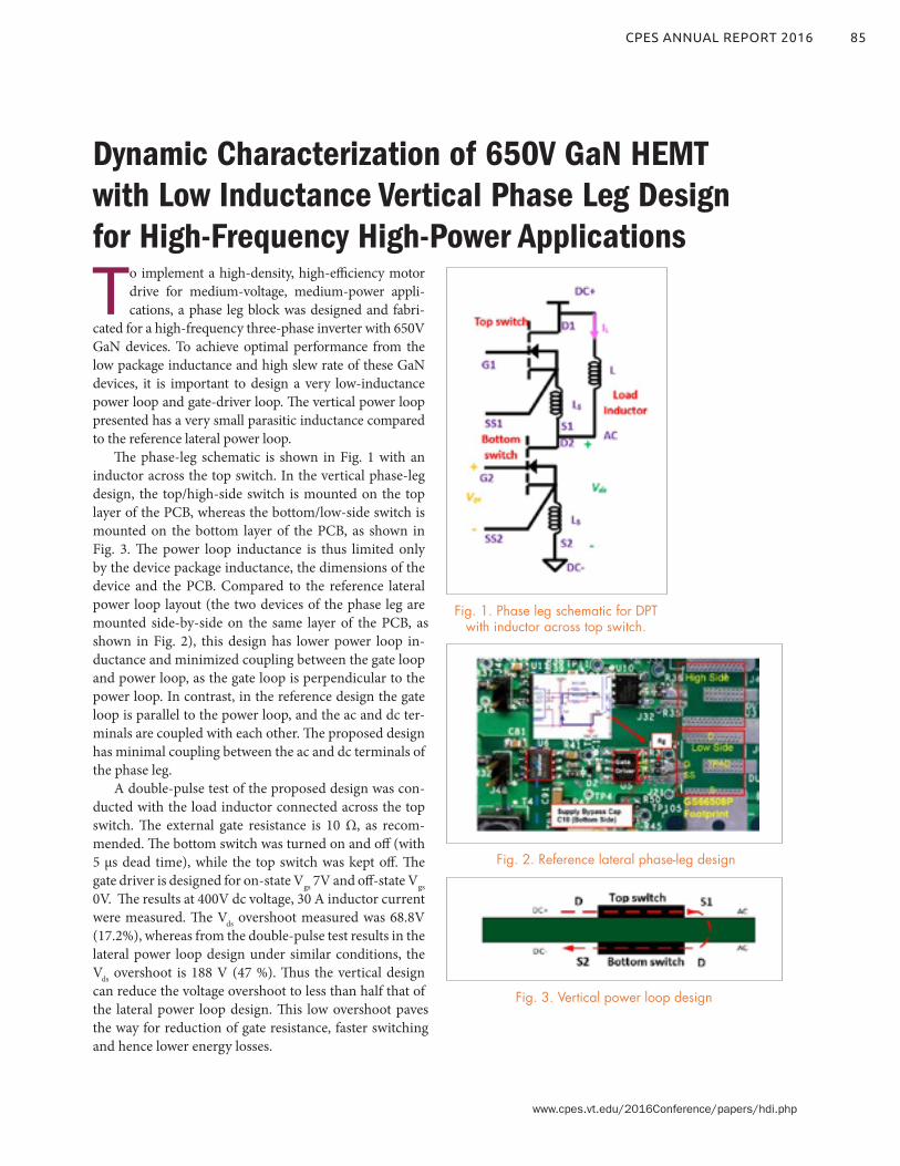
85CPES ANNUAL REPORT 2016
www.cpes.vt.edu/2016Conference/papers/hdi.php
To implement a high-density, high-efficiency motor drive for medium-voltage, medium-power appli-cations, a phase leg block was designed and fabri-
cated for a high-frequency three-phase inverter with 650V GaN devices. To achieve optimal performance from the low package inductance and high slew rate of these GaN devices, it is important to design a very low-inductance power loop and gate-driver loop. The vertical power loop presented has a very small parasitic inductance compared to the reference lateral power loop.
The phase-leg schematic is shown in Fig. 1 with an inductor across the top switch. In the vertical phase-leg design, the top/high-side switch is mounted on the top layer of the PCB, whereas the bottom/low-side switch is mounted on the bottom layer of the PCB, as shown in Fig. 3. The power loop inductance is thus limited only by the device package inductance, the dimensions of the device and the PCB. Compared to the reference lateral power loop layout (the two devices of the phase leg are mounted side-by-side on the same layer of the PCB, as shown in Fig. 2), this design has lower power loop in-ductance and minimized coupling between the gate loop and power loop, as the gate loop is perpendicular to the power loop. In contrast, in the reference design the gate loop is parallel to the power loop, and the ac and dc ter-minals are coupled with each other. The proposed design has minimal coupling between the ac and dc terminals of the phase leg.
A double-pulse test of the proposed design was con-ducted with the load inductor connected across the top switch. The external gate resistance is 10 Ω, as recom-mended. The bottom switch was turned on and off (with 5 µs dead time), while the top switch was kept off. The gate driver is designed for on-state Vgs 7V and off-state Vgs 0V. The results at 400V dc voltage, 30 A inductor current were measured. The Vds overshoot measured was 68.8V (17.2%), whereas from the double-pulse test results in the lateral power loop design under similar conditions, the Vds overshoot is 188 V (47 %). Thus the vertical design can reduce the voltage overshoot to less than half that of the lateral power loop design. This low overshoot paves the way for reduction of gate resistance, faster switching and hence lower energy losses.
Dynamic Characterization of 650V GaN HEMT with Low Inductance Vertical Phase Leg Design for High-Frequency High-Power Applications
Fig. 1. Phase leg schematic for DPT with inductor across top switch.
Fig. 2. Reference lateral phase-leg design
Fig. 3. Vertical power loop design
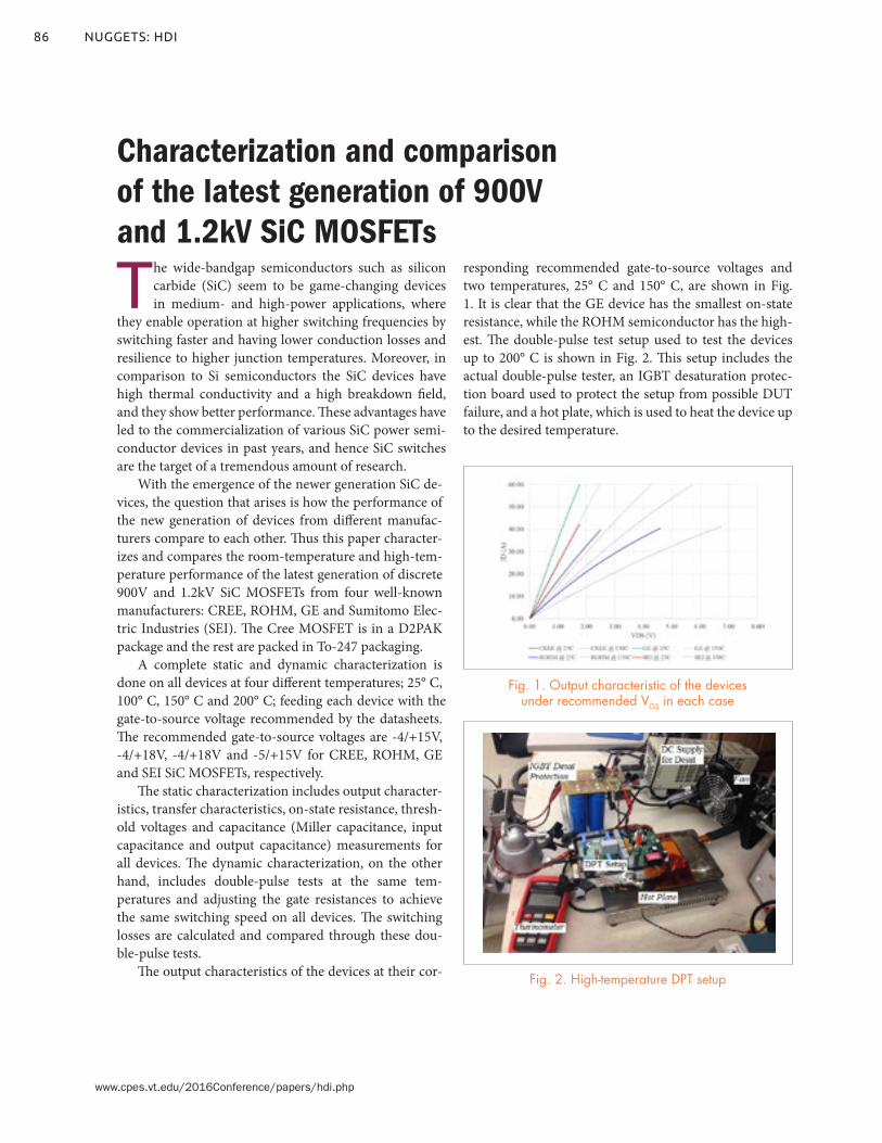
86 NUGGETS: HDI
www.cpes.vt.edu/2016Conference/papers/hdi.php
The wide-bandgap semiconductors such as silicon carbide (SiC) seem to be game-changing devices in medium- and high-power applications, where
they enable operation at higher switching frequencies by switching faster and having lower conduction losses and resilience to higher junction temperatures. Moreover, in comparison to Si semiconductors the SiC devices have high thermal conductivity and a high breakdown field, and they show better performance. These advantages have led to the commercialization of various SiC power semi-conductor devices in past years, and hence SiC switches are the target of a tremendous amount of research.
With the emergence of the newer generation SiC de-vices, the question that arises is how the performance of the new generation of devices from different manufac-turers compare to each other. Thus this paper character-izes and compares the room-temperature and high-tem-perature performance of the latest generation of discrete 900V and 1.2kV SiC MOSFETs from four well-known manufacturers: CREE, ROHM, GE and Sumitomo Elec-tric Industries (SEI). The Cree MOSFET is in a D2PAK package and the rest are packed in To-247 packaging.
A complete static and dynamic characterization is done on all devices at four different temperatures; 25° C, 100° C, 150° C and 200° C; feeding each device with the gate-to-source voltage recommended by the datasheets. The recommended gate-to-source voltages are -4/+15V, -4/+18V, -4/+18V and -5/+15V for CREE, ROHM, GE and SEI SiC MOSFETs, respectively.
The static characterization includes output character-istics, transfer characteristics, on-state resistance, thresh-old voltages and capacitance (Miller capacitance, input capacitance and output capacitance) measurements for all devices. The dynamic characterization, on the other hand, includes double-pulse tests at the same tem-peratures and adjusting the gate resistances to achieve the same switching speed on all devices. The switching losses are calculated and compared through these dou-ble-pulse tests.
The output characteristics of the devices at their cor-
responding recommended gate-to-source voltages and two temperatures, 25° C and 150° C, are shown in Fig. 1. It is clear that the GE device has the smallest on-state resistance, while the ROHM semiconductor has the high-est. The double-pulse test setup used to test the devices up to 200° C is shown in Fig. 2. This setup includes the actual double-pulse tester, an IGBT desaturation protec-tion board used to protect the setup from possible DUT failure, and a hot plate, which is used to heat the device up to the desired temperature.
Characterization and comparison of the latest generation of 900V and 1.2kV SiC MOSFETs
Fig. 1. Output characteristic of the devices under recommended VGS in each case
Fig. 2. High-temperature DPT setup

87CPES ANNUAL REPORT 2016
www.cpes.vt.edu/2016Conference/papers/hdi.php
In the field of power electronics, due to constraints such as power quality and power density, it has always been of special interest to switch devices at the highest pos-
sible switching frequencies. However, until the past decade, the existing medium-voltage semiconductors were unable to have a switching frequency beyond a few hundred kilo-hertz, and the conduction loss was quite high. Since their introduction, SiC semiconductors have been of special in-terest in power electronics, since they enable higher switch-ing frequencies, higher junction temperatures and higher voltages; thus being considered game-changing devices.
SiC semiconductors are in the early stages of their evolution, and, especially at higher voltages, they are not yet fully developed. However, device manufacturers are doing research and producing sample devices now that will finally lead to commercial SiC semiconductors. The ultimate goal of this paper is to characterize and compare four sample SiC MOSFETs at 3.3-kV 30A in a TO-247 full-mold package that includes a single die inside. The received samples have part numbers D10, D14, T10 and P12, and will be referred to with these names in figures and tables.
This paper characterizes and compares the room-temperature and high-temperature performances of the mentioned MOSFETs. A complete static and dynamic characterization is done on all devices at the tempera-tures 25° C, 100° C and 150° C, feeding the devices with their datasheet-recommended -5/+15V gate-to-source voltage. The static characterization includes output char-acteristics, transfer characteristics, on-state resistances, threshold voltages and capacitance measurements. The dynamic characterization, on the other hand, includes double-pulse tests at the same temperatures at four dif-ferent gate resistances to achieve loss variation according to the gate resistance for the devices. The switching losses
are calculated and compared through these double-pulse tests.
The output characteristics of the devices under test are shown in Fig. 1 at 25° C and 150° C. The results show that the MOSFETs D10 and T10 have a similar structure. In addition, the D14 and P12 devices show similar char-acteristics at both room temperature and high tempera-ture.
Fig. 2 shows the double-pulse test setup used to do the dynamic characterization. The capacitors are con-nected via busbar, an IGBT desaturation overcurrent protection is used for possible DUT failure protection, and the load inductor and the actual double-pulse tester PCB can be seen. The gate signal is optically isolated for safety considerations.
Static and dynamic performance characterization of 3.3-kV 30A discrete SiC MOSFETs from Sumitomo Electric Industries
Fig. 1. Output characteristic of 3.3kV SiC MOSFETs under recommended VGS at 25° C and 150° C
Fig. 2. Double-pulse test setup used for dynamic characterization of 3.3kV SiC MOSFETs
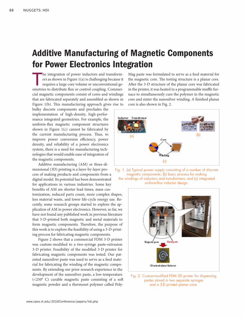
88 NUGGETS: HDI
www.cpes.vt.edu/2016Conference/papers/hdi.php
The integration of power inductors and transform-ers as shown in Figure 1(a) is challenging because it requires a large core volume or unconventional ge-
ometries to distribute flux or control coupling. Commer-cial magnetic components consist of cores and windings that are fabricated separately and assembled as shown in Figure 1(b). This manufacturing approach gives rise to bulky discrete components and precludes the implementation of high-density, high-perfor-mance integrated geometries. For example, the uniform-flux magnetic component structures shown in Figure 1(c) cannot be fabricated by the current manufacturing process. Thus, to improve power conversion efficiency, power density, and reliability of a power electronics system, there is a need for manufacturing tech-nologies that would enable ease of integration of the magnetic components.
Additive manufacturing (AM) or three-di-mensional (3D) printing is a layer-by-layer pro-cess of making products and components from a digital model. Its potential has been demonstrated for applications in various industries. Some key benefits of AM are shorter lead times, mass cus-tomization, reduced parts count, more complex shapes, less material waste, and lower life-cycle energy use. Re-cently, some research groups started to explore the ap-plication of AM in power electronics. However, so far, we have not found any published work in previous literature that 3-D-printed both magnetic and metal materials to form magnetic components. Therefore, the purpose of this work is to explore the feasibility of using a 3-D-print-ing process for fabricating magnetic components.
Figure 2 shows that a commercial FDM 3-D printer was custom-modified to a two-syringe paste-extrusion 3-D printer. Feasibility of the modified 3-D printer for fabricating magnetic components was tested. Our pat-ented nanosilver paste was used to serve as a feed mate-rial for fabricating the winding of the magnetic compo-nents. By extending our prior research experience in the development of the nanosilver paste, a low-temperature (<250° C) curable magnetic paste consisting of a soft magnetic powder and a thermoset polymer called Poly-
Mag paste was formulated to serve as a feed material for the magnetic core. The testing structure is a planar core. After the 3-D structure of the planar core was fabricated in the printer, it was heated in a programmable muffle fur-nace to simultaneously cure the polymer in the magnetic core and sinter the nanosilver winding. A finished planar core is also shown in Fig. 2.
Additive Manufacturing of Magnetic Components for Power Electronics Integration
Fig. 1. (a) Typical power supply consisting of a number of discrete magnetic components; (b) basic process for making
the windings of inductors and transformers; and (c) integrated uniform-flux inductor design.
Fig. 2. Custom-modified FDM 3D printer for dispensing pastes stored in two separate syringes
and a 3-D printed planar core.
(a)
(c)
(b)
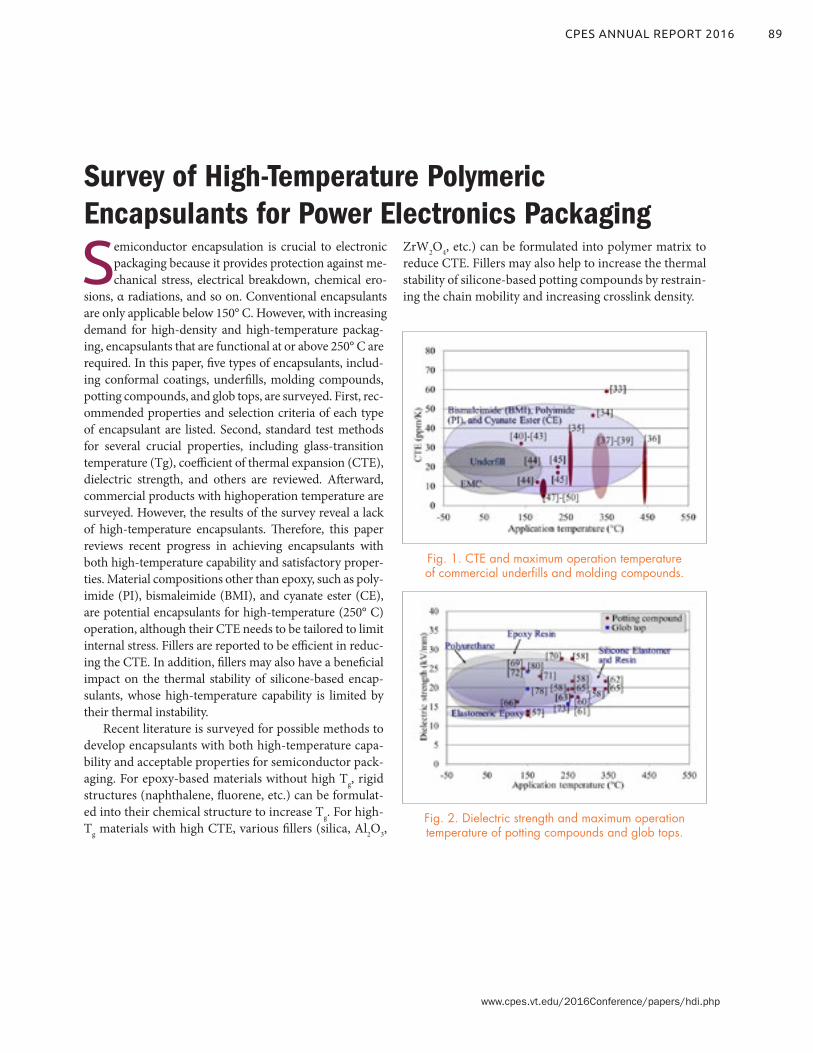
89CPES ANNUAL REPORT 2016
www.cpes.vt.edu/2016Conference/papers/hdi.php
Semiconductor encapsulation is crucial to electronic packaging because it provides protection against me-chanical stress, electrical breakdown, chemical ero-
sions, α radiations, and so on. Conventional encapsulants are only applicable below 150° C. However, with increasing demand for high-density and high-temperature packag-ing, encapsulants that are functional at or above 250° C are required. In this paper, five types of encapsulants, includ-ing conformal coatings, underfills, molding compounds, potting compounds, and glob tops, are surveyed. First, rec-ommended properties and selection criteria of each type of encapsulant are listed. Second, standard test methods for several crucial properties, including glass-transition temperature (Tg), coefficient of thermal expansion (CTE), dielectric strength, and others are reviewed. Afterward, commercial products with highoperation temperature are surveyed. However, the results of the survey reveal a lack of high-temperature encapsulants. Therefore, this paper reviews recent progress in achieving encapsulants with both high-temperature capability and satisfactory proper-ties. Material compositions other than epoxy, such as poly-imide (PI), bismaleimide (BMI), and cyanate ester (CE), are potential encapsulants for high-temperature (250° C) operation, although their CTE needs to be tailored to limit internal stress. Fillers are reported to be efficient in reduc-ing the CTE. In addition, fillers may also have a beneficial impact on the thermal stability of silicone-based encap-sulants, whose high-temperature capability is limited by their thermal instability.
Recent literature is surveyed for possible methods to develop encapsulants with both high-temperature capa-bility and acceptable properties for semiconductor pack-aging. For epoxy-based materials without high Tg, rigid structures (naphthalene, fluorene, etc.) can be formulat-ed into their chemical structure to increase Tg. For high-Tg materials with high CTE, various fillers (silica, Al2O3,
ZrW2O4, etc.) can be formulated into polymer matrix to reduce CTE. Fillers may also help to increase the thermal stability of silicone-based potting compounds by restrain-ing the chain mobility and increasing crosslink density.
Survey of High-Temperature Polymeric Encapsulants for Power Electronics Packaging
Fig. 1. CTE and maximum operation temperature of commercial underfills and molding compounds.
Fig. 2. Dielectric strength and maximum operation temperature of potting compounds and glob tops.

90 NUGGETS: HDI
www.cpes.vt.edu/2016Conference/papers/hdi.php
With current limited by their small size, SiC MOSFETs are paralleled to achieve high cur-rent rating and power density. However, a mis-
match in parameters can cause unbalanced junction tem-perature and drain current distribution, which may affect the reliability and longevity of the devices. Usually extra components or strategies are introduced to attenuate the unbalance, which significantly increases the cost and the complexity of the system with more MOSFETs in parallel. Therefore, electro-thermal distribution among paralleled SiC MOSFETs is analyzed based on simulation and ex-periment to find out useful intrinsic properties hidden in the SiC MOSFET.
Simulation is based on LTspice. Compared with tra-ditional simulation, electro-thermal simulation is more accurate for the simulations that involve tem-peratures. However, mismatch information cannot be found in the Spice model provided by the manufac-turer. After modifying, the Spice model of SiC MOS-FETs with mismatch in the threshold voltage (Vth) and on-resistance (Rds(on)) are created. The range of mismatches is obtained from a technical report from the manufacturer. After that, two paralleled SiC MOS-FETs with a mismatch are applied in a boost converter in LTspice to test the temperature and current unbal-ance. Furthermore, to reduce the unbalance, a New-ton-Raphson iteration-based calculation, which has little operating time and calculation error, is applied to replace time-consuming electro-thermal simula-tion. The current and temperature distribution among two paralleled SiC MOSFETs can be obtained by look-ing at Fig. 1.
Considering that in a SiC MOSFET a temperature rise causes Rds(on) to increase and Vth to decrease, the positive temperature coefficient (PTC) of Rds(on) can help balance the difference in conduction loss. How-ever, although it seems that a negative temperature co-efficient (NTC) of Vth will degrade the switching loss balancing with a higher temperature, in simulation the difference in switching loss is almost constant with temperature increasing. To summarize, the difference of switching loss caused by a mismatch of Vth is the source of unbalance in temperature, and the PTC of
Rds(on) is the intrinsic balancing ability in SiC MOSFETs. Whether the PTC can compensate the unbalance is deter-mined by the ratio of the switching loss and conduction loss. If the conduction loss is high enough, the balancing ability caused by PTC is strong enough to compensate the power difference, and vice versa.
A two-level experiment is used to verify previous analysis and calculation results. First, the component pa-rameters are measured to verify the previous mismatch range and re-guide simulation (calculation). Based on the previous measurement, samples with obvious mismatches are inserted in a boost converter to verify the calculation results in regard to current and temperature distribution. The experiment platform is shown in Fig. 2.
Electro-Thermal Distribution among Paralleled SiC MOSFETs
Fig. 1. Calculation results of temperature and current distribution of two paralleled MOSFETs in boost converter.
Fig. 2. Experiment platform.
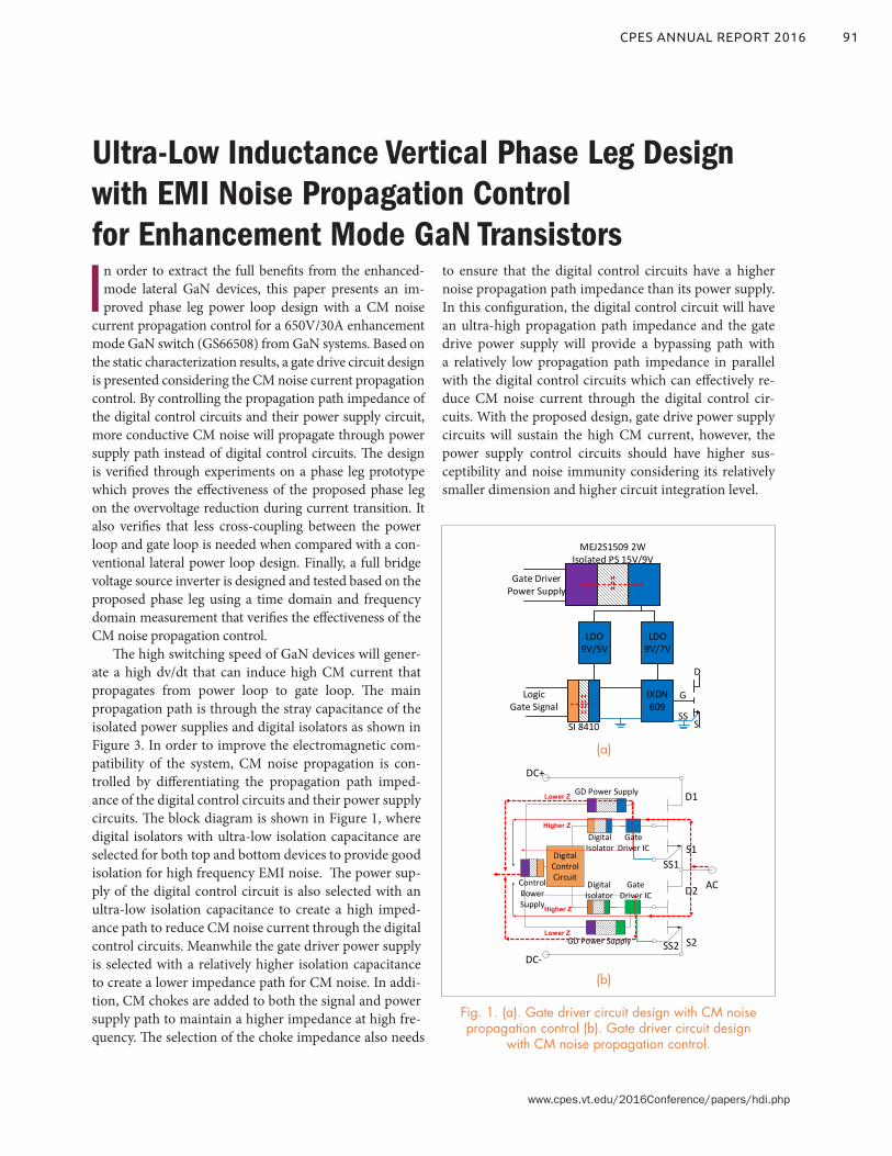
91CPES ANNUAL REPORT 2016
www.cpes.vt.edu/2016Conference/papers/hdi.php
In order to extract the full benefits from the enhanced-mode lateral GaN devices, this paper presents an im-proved phase leg power loop design with a CM noise
current propagation control for a 650V/30A enhancement mode GaN switch (GS66508) from GaN systems. Based on the static characterization results, a gate drive circuit design is presented considering the CM noise current propagation control. By controlling the propagation path impedance of the digital control circuits and their power supply circuit, more conductive CM noise will propagate through power supply path instead of digital control circuits. The design is verified through experiments on a phase leg prototype which proves the effectiveness of the proposed phase leg on the overvoltage reduction during current transition. It also verifies that less cross-coupling between the power loop and gate loop is needed when compared with a con-ventional lateral power loop design. Finally, a full bridge voltage source inverter is designed and tested based on the proposed phase leg using a time domain and frequency domain measurement that verifies the effectiveness of the CM noise propagation control.
The high switching speed of GaN devices will gener-ate a high dv/dt that can induce high CM current that propagates from power loop to gate loop. The main propagation path is through the stray capacitance of the isolated power supplies and digital isolators as shown in Figure 3. In order to improve the electromagnetic com-patibility of the system, CM noise propagation is con-trolled by differentiating the propagation path imped-ance of the digital control circuits and their power supply circuits. The block diagram is shown in Figure 1, where digital isolators with ultra-low isolation capacitance are selected for both top and bottom devices to provide good isolation for high frequency EMI noise. The power sup-ply of the digital control circuit is also selected with an ultra-low isolation capacitance to create a high imped-ance path to reduce CM noise current through the digital control circuits. Meanwhile the gate driver power supply is selected with a relatively higher isolation capacitance to create a lower impedance path for CM noise. In addi-tion, CM chokes are added to both the signal and power supply path to maintain a higher impedance at high fre-quency. The selection of the choke impedance also needs
to ensure that the digital control circuits have a higher noise propagation path impedance than its power supply. In this configuration, the digital control circuit will have an ultra-high propagation path impedance and the gate drive power supply will provide a bypassing path with a relatively low propagation path impedance in parallel with the digital control circuits which can effectively re-duce CM noise current through the digital control cir-cuits. With the proposed design, gate drive power supply circuits will sustain the high CM current, however, the power supply control circuits should have higher sus-ceptibility and noise immunity considering its relatively smaller dimension and higher circuit integration level.
Ultra-Low Inductance Vertical Phase Leg Design with EMI Noise Propagation Control for Enhancement Mode GaN Transistors
LDO9V/5V
LDO9V/7V
IXDN 609
D
G
SSS
MEJ2S1509 2W Isolated PS 15V/9V
SI 8410
Gate Driver Power Supply
Logic Gate Signal
D1
D2
S2SS2
SS1
DC+
DC-
AC
Digital Control Circuit
Digital Isolator
Gate Driver IC
Digital Isolator S1
GD Power Supply
GD Power Supply
Gate Driver IC
Control Power Supply
Higher Z
Lower Z
Higher Z
Lower Z
Fig. 1. (a). Gate driver circuit design with CM noise propagation control (b). Gate driver circuit design
with CM noise propagation control.
(a)
(b)
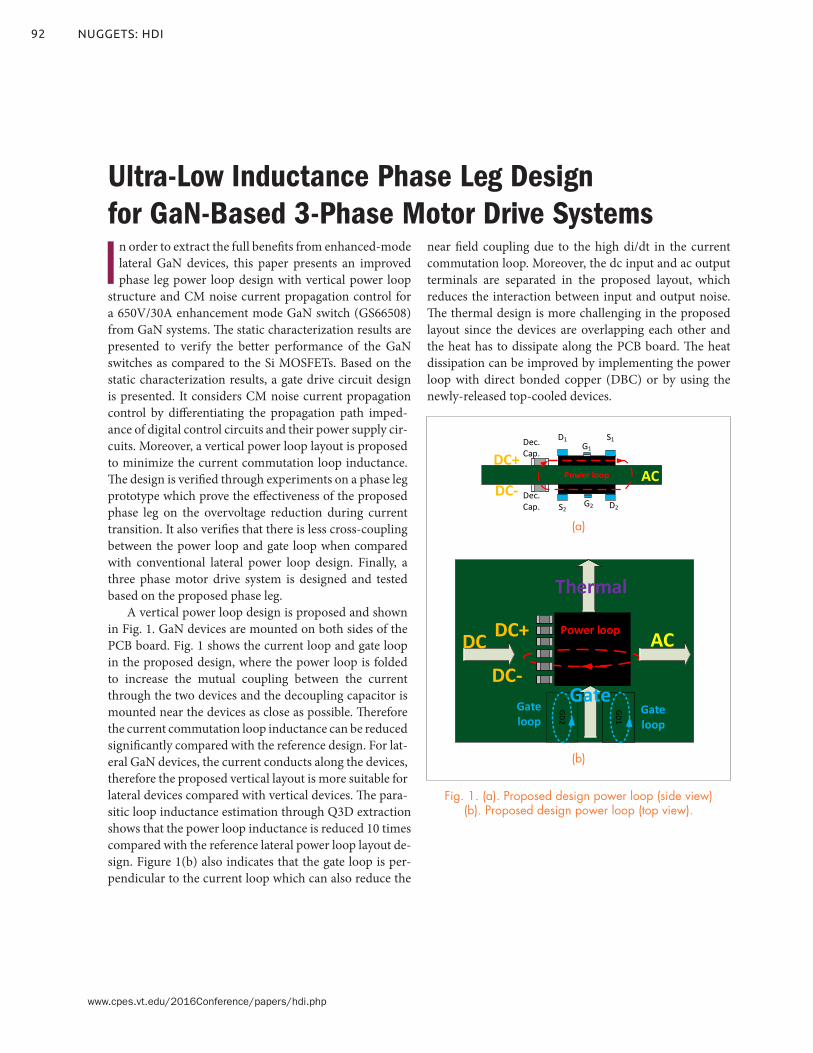
92 NUGGETS: HDI
www.cpes.vt.edu/2016Conference/papers/hdi.php
In order to extract the full benefits from enhanced-mode lateral GaN devices, this paper presents an improved phase leg power loop design with vertical power loop
structure and CM noise current propagation control for a 650V/30A enhancement mode GaN switch (GS66508) from GaN systems. The static characterization results are presented to verify the better performance of the GaN switches as compared to the Si MOSFETs. Based on the static characterization results, a gate drive circuit design is presented. It considers CM noise current propagation control by differentiating the propagation path imped-ance of digital control circuits and their power supply cir-cuits. Moreover, a vertical power loop layout is proposed to minimize the current commutation loop inductance. The design is verified through experiments on a phase leg prototype which prove the effectiveness of the proposed phase leg on the overvoltage reduction during current transition. It also verifies that there is less cross-coupling between the power loop and gate loop when compared with conventional lateral power loop design. Finally, a three phase motor drive system is designed and tested based on the proposed phase leg.
A vertical power loop design is proposed and shown in Fig. 1. GaN devices are mounted on both sides of the PCB board. Fig. 1 shows the current loop and gate loop in the proposed design, where the power loop is folded to increase the mutual coupling between the current through the two devices and the decoupling capacitor is mounted near the devices as close as possible. Therefore the current commutation loop inductance can be reduced significantly compared with the reference design. For lat-eral GaN devices, the current conducts along the devices, therefore the proposed vertical layout is more suitable for lateral devices compared with vertical devices. The para-sitic loop inductance estimation through Q3D extraction shows that the power loop inductance is reduced 10 times compared with the reference lateral power loop layout de-sign. Figure 1(b) also indicates that the gate loop is per-pendicular to the current loop which can also reduce the
near field coupling due to the high di/dt in the current commutation loop. Moreover, the dc input and ac output terminals are separated in the proposed layout, which reduces the interaction between input and output noise. The thermal design is more challenging in the proposed layout since the devices are overlapping each other and the heat has to dissipate along the PCB board. The heat dissipation can be improved by implementing the power loop with direct bonded copper (DBC) or by using the newly-released top-cooled devices.
Ultra-Low Inductance Phase Leg Design for GaN-Based 3-Phase Motor Drive Systems
DC+
DC-ACPower loop
Dec. Cap.
Dec. Cap.
D1 S1
D2S2G2
G1
GD1
GD2
DC+
DC-
ACDC
Gate
Thermal
Gateloop
Gateloop
Power loop
Fig. 1. (a). Proposed design power loop (side view) (b). Proposed design power loop (top view).
(a)
(b)

93CPES ANNUAL REPORT 2016
www.cpes.vt.edu/2016Conference/papers/hdi.php
This paper presents the inductor loss minimization for interleaved boost converters in electric vehicle applications. Equivalent circuits are presented to an-
alyze the steady state working condition of the inductors in interleaving topology with and without coupled inductors. With the proposed equivalent circuits, the inductor work-ing condition can be predicted for both boost inductors and coupled inductors. Based on the predicted inductor working conditions, an inductor loss modeling is present-ed considering detailed dc and ac winding loss modeling and core loss calculation with an improved generalized Steinmetz equation. The passive component loss mini-mization method is presented to explore the optimized coupled inductance for a total inductor loss minimization. Experimental verification is conducted based on a 1kW interleaved dc-dc boost converter.
A two phase interleaved dc-dc boost converter with an ideal reverse coupled inductor is shown in Fig. 2, where the carrier of converter 2 is phase shifted by 180°. With the phase-shifting of the gate signals, the current ripple of each converter is also phase-shifted, thus caus-ing the total current ripple to be reduced. The inductors are separated as the non-coupled inductor L and ideal coupled inductor M. When the two converters are cou-pled together, the current through each inductor can be separated as output current Iout and circulating current Icir. With the equivalent circuit shown in the previous sec-tion, inductor operation conditions including inductor current waveform and voltage excitation can be predicted by adding different coupled inductance to the circuit. In-ductor loss can be calculated with the information of the inductor operation conditions. Figure 2 shows the total inductor loss changes when a different coupled induc-tor is added to the circuit. Adding a coupled inductor can reduce the boost inductor loss significantly, but the added coupled inductor will also have additional loss-es. Increasing the coupled inductance will decrease the boost inductor loss and increase the loss on the coupled inductor, however the effectiveness is reduced when the coupled inductance is large enough and there is an op-timal coupled inductance for minimized total inductor loss for interleaved boost dc-dc converters. In order to verify the analysis above, a 1kW interleaved dc-dc boost
converter is implemented and tested with different boost and coupled inductors. Figure 3 presents the measured inductor losses for both boost and coupled inductors, which indicate that the total passive component losses is achieved when coupled inductance is 8mH for the experi-mental prototype.
Passive Component Loss Minimization for Interleaved dc-dc Boost Converters in Electric Vehicle Applications
Battery L2 MVin
V1
V2
IcirIout
L1 M
Fig. 1. Interleaved dc-dc converter with coupled inductor.
Fig. 2. Calculated inductor loss with different coupled inductance M (normalized
to total loss without coupled inductor).
132.1
24.08 19.78
0
83.7 106.4
020406080
100120140
M=0 M=8 mH M=40 mH
Passive Componet Loss (mW)
L M
Fig. 3. Passive component loss comparison with different M.
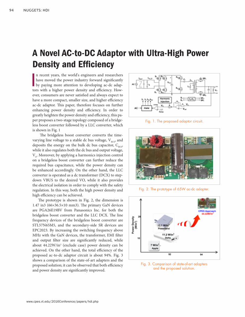
94 NUGGETS: HDI
www.cpes.vt.edu/2016Conference/papers/hdi.php
A Novel AC-to-DC Adaptor with Ultra-High Power Density and Efficiency
In recent years, the world's engineers and researchers have moved the power industry forward significantly by paying more attention to developing ac-dc adap-
tors with a higher power density and efficiency. How-ever, consumers are never satisfied and always expect to have a more compact, smaller size, and higher efficiency ac-dc adaptor. This paper, therefore focuses on further enhancing power density and efficiency. In order to greatly heighten the power density and efficiency, this pa-per proposes a two-stage topology composed of a bridge-less boost converter followed by a LLC converter, which is shown in Fig. 1
The bridgeless boost converter converts the time-varying line voltage to a stable dc bus voltage, VBUS, and deposits the energy on the bulk dc bus capacitor, CBUS, while it also regulates both the dc bus and output voltage, VO. Moreover, by applying a harmonics injection control on a bridgeless boost converter can further reduce the required bus capacitance, while the power density can be enhanced accordingly. On the other hand, the LLC converter is operated as a dc transformer (DCX) to step-down VBUS to the desired VO, while it also provides the electrical isolation in order to comply with the safety regulation. In this way, both the high power density and high efficiency can be achieved.
The prototype is shown in Fig. 2, the dimension is 1.47 in3 (66×36.5×10 mm3). The primary GaN devices are PGA26E19BV from Panasonics Inc. for both the bridgeless boost converter and the LLC DCX. The line frequency devices of the bridgeless boost converter are STL57N65M5, and the secondary-side SR devices are EPC2023. By increasing the switching frequency above MHz with the GaN devices, the transformer, EMI filter and output filter size are significantly reduced, while about 44.22W/in3 (exclude case) power density can be achieved. On the other hand, the total efficiency of the proposed ac-to-dc adaptor circuit is about 94%. Fig. 3 shows a comparison of the state-of-art adapters and the proposed solution; it can be observed that both efficiency and power density are significantly improved.
Fig. 1. The proposed adaptor circuit.
Fig. 2. The prototype of 65W ac-dc adapter.
Fig. 3. Comparison of state-of-art adapters and the proposed solution.

Renewable Energy & Nanogrids NuggetsLow Frequency Common Mode Voltage Control for Systems Interconnected with Power Converters
Synchronous Machine-Based Multi-Converter System With Online Interaction Monitoring Function
Modeling and Control of Grid-Connected Voltage Source Converters Emulating Isotropic and Anisotropic Synchronous Machines
Modular Scalable Medium-voltage Imped-ance Measurement Unit Using 10kV SiC MOSFET PEBBs
Voltage Controlled Converter Emulating Synchronous Machine - Model Verification
Analysis of Phase-Locked Loop Low-Frequency Stability in Three-Phase Grid-Connected Power Converters Considering Impedance Interactions
State Trajectory Analysis of Modular Mul-tilevel Converter
Design, Analysis and Experimental Evalu-ation of a Virtual-Synchronous-Machine-Based STATCOM with LCL Filter
Small-Signal Terminal Characteristics Modeling of Three-Phase Boost Rectifier with Variable Fundamental Frequency
Normalized Design Method for Coils in Series-Series Inductive Power Transfer System
Capacitor Voltage Ripple Reduction for Modular Multilevel Converter with 2nd or-der Current Injection and Over Modulation
Analysis of Capacitor Voltage Ripple Mini-mization in Modular Multilevel Converter Based on Average Model
Magnetic Materials Selection Procedure for Coupled Inductor used in Interleaved Three-level Multi-phase DC-DC Converters
Study on Three-level DC/DC Converter with Coupled Inductors
Model-Based Design of a Modular Mul-tilevel Converter with Minimized Design Margins
Small-signal Impedance Measurement in Medium-voltage DC Power Systems
Design of a Modular and Scalable Small-signal dq Impedance Measurement Unit for Grid Applications Utilizing 10 kV SiC MOSFETs
Assessment of Medium Voltage Distribu-tion Feeders under High Penetration of PV Generation
Modeling and Analysis of High Frequency Interactions for Distributed Power System
REN Research TeamFebruary 2015 – February 2016
FacultyDushan BoroyevichRolando BurgosFred C. LeeQiang Li
Research FacultyIgor CvetkovicMingkai MuZhiyu Shen
Graduate StudentsFang Chen Yi-Hsun (Eric) HsiehZhengrong HuangMarko JaksicYang JiaoChen LiChi LiYadong LyuAlinaghi MarzoughiSungjae OhnRuiyang QinNiloofar Rashidi Ye TangJun WangBo WenWei Zhang
Visiting ScholarsZeng LiuGabriele RizzoliXiaolong Yue
95CPES ANNUAL REPORT 2016
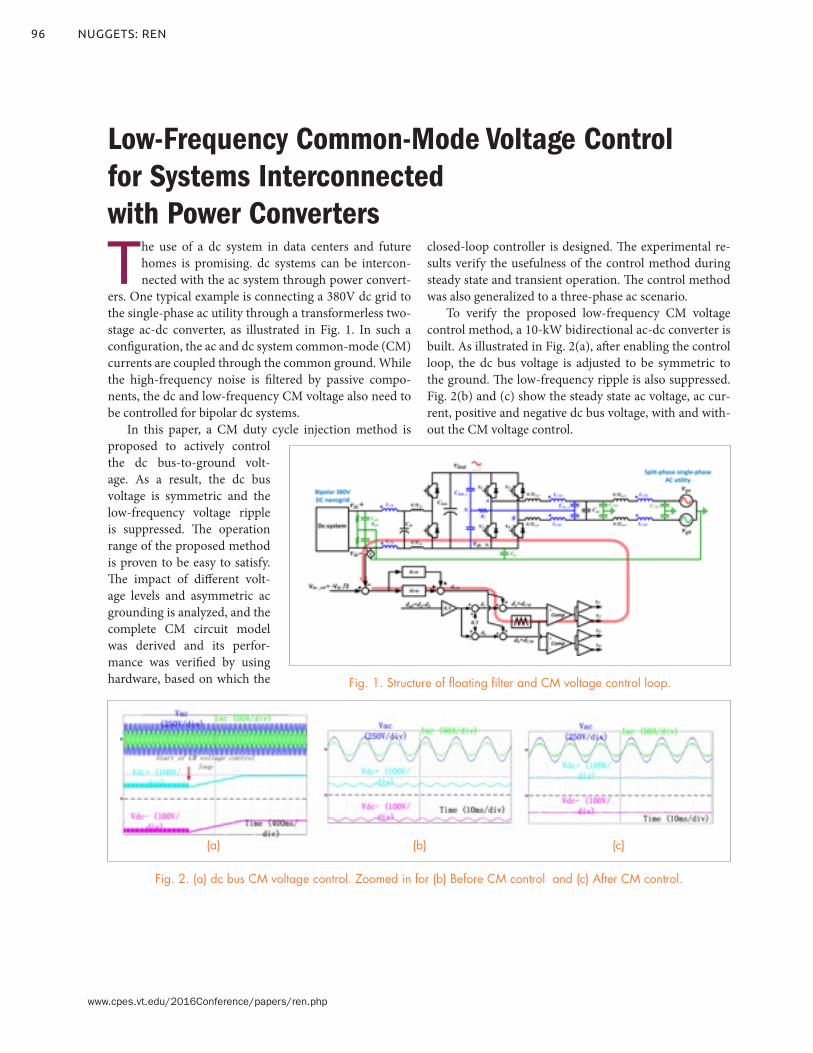
96
www.cpes.vt.edu/2016Conference/papers/ren.php
NUGGETS: REN
The use of a dc system in data centers and future homes is promising. dc systems can be intercon-nected with the ac system through power convert-
ers. One typical example is connecting a 380V dc grid to the single-phase ac utility through a transformerless two-stage ac-dc converter, as illustrated in Fig. 1. In such a configuration, the ac and dc system common-mode (CM) currents are coupled through the common ground. While the high-frequency noise is filtered by passive compo-nents, the dc and low-frequency CM voltage also need to be controlled for bipolar dc systems.
In this paper, a CM duty cycle injection method is proposed to actively control the dc bus-to-ground volt-age. As a result, the dc bus voltage is symmetric and the low-frequency voltage ripple is suppressed. The operation range of the proposed method is proven to be easy to satisfy. The impact of different volt-age levels and asymmetric ac grounding is analyzed, and the complete CM circuit model was derived and its perfor-mance was verified by using hardware, based on which the
closed-loop controller is designed. The experimental re-sults verify the usefulness of the control method during steady state and transient operation. The control method was also generalized to a three-phase ac scenario.
To verify the proposed low-frequency CM voltage control method, a 10-kW bidirectional ac-dc converter is built. As illustrated in Fig. 2(a), after enabling the control loop, the dc bus voltage is adjusted to be symmetric to the ground. The low-frequency ripple is also suppressed. Fig. 2(b) and (c) show the steady state ac voltage, ac cur-rent, positive and negative dc bus voltage, with and with-out the CM voltage control.
Low-Frequency Common-Mode Voltage Control for Systems Interconnected with Power Converters
Fig. 1. Structure of floating filter and CM voltage control loop.
Fig. 2. (a) dc bus CM voltage control. Zoomed in for (b) Before CM control and (c) After CM control.
(b)(a) (c)

97CPES ANNUAL REPORT 2016
www.cpes.vt.edu/2016Conference/papers/ren.php
The advancement of power electronics has been a key enabler of the vast proliferation of renewable energy sources in the electrical power grid over the past sev-
eral years, acting both as an energy source interface and as compensation asset in HVDC and FACTS-supported ac systems for energy transport. This trend, together with the ever-increasing deployment of electronically interfaced loads, as well as the increasing penetration of microgrids, is fundamentally changing the nature of the sources and the loads in the electrical grid, altering their conventionally mild aggregate dynamics, and inflicting low- and high-fre-quency dynamic interactions that did not exist before. Consequently, high dispersion of power electronics into the future grid will largely depend on engineers’ capabil-ity to understand, model, and dynamically control power sharing and subsystem inter-actions.
With the recent revision of the IEEE 1547 standard to allow distributed genera-tion to regulate voltage at the point of com-mon coupling, numerous research groups have started exploring unconventional ways to control grid-interface converters. Such a change requires new concepts for advanced control of all energy flows in or-
der to improve system stability, energy availability, and reliability. This paper presents a grid-interface converter that behaves as a synchronous machine, and shows how its adaptive virtual inertia can mitigate instability caused by partial loss of generation. Additionally, it shows one of the ways to implement an online stability monitoring function by observing small-signal active and reactive power at the converter terminals.
Synchronous Machine-Based Multi-Converter System with Online Interaction Monitoring Function
Fig. 1. Two-source and two-load-interconnected system as a benchmark for online stability monitoring.
Fig. 2. (a) Bode plots of small-signal active and (b) reactive power for both stable and unstable cases.
(b)(a)

98
www.cpes.vt.edu/2016Conference/papers/ren.php
NUGGETS: REN
With the recent revision of the IEEE 1547 standard so that it now, for the first time, allows distributed gen-
eration to regulate voltage at the point of com-mon coupling, a number of research groups have started exploring unconventional ways to control grid-interface converters. This kind of change requires new concepts for the advanced control of all energy flows in order to improve system stability, energy availability, and efficien-cy. Consequently, high adoption of renewable energy sources will greatly depend on engineers’ capability to understand, model, and dynamical-ly control power sharing and subsystem interac-tions. This paper presents an informed method of controlling power converters as synchronous machines of any type in the d-q coordinate sys-tem by formally establishing electromechanical-electrical duality, which requires an understand-ing of which parameters of power converters relate to which parameters of isotropic or aniso-tropic synchronous machines.
The paper describes a generic d-q model of the grid-interface converter that behaves as a synchronous machine of any type, and shows how to control power converters in the d-q frame in order to emulate both isotropic and anisotro-pic machines with more than one damper wind-ing. It also shows that d-q transformation (and converter synchronization) can be done by using an internal angle obtained by integrating dc-link voltage, and how to realize the concept of virtual inertia. The model developed can be used for the system-level simulations to address grid system stability and performance improvement.
Modeling and Control of Grid-Connected Voltage Source Converters Emulating Isotropic and Anisotropic Synchronous Machines
Fig. 1. Grid-interface converter that behaves as a synchronous machine.
Fig. 2. Power converter-based d-q average model of the synchronous machine, and an average d-q average
model of the power converter.
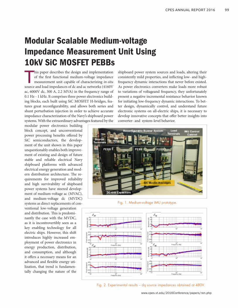
99CPES ANNUAL REPORT 2016
www.cpes.vt.edu/2016Conference/papers/ren.php
This paper describes the design and implementation of the first functional medium-voltage impedance measurement unit capable of characterizing in-situ
source and load impedances of dc and ac networks (4160V ac, 6000V dc, 300 A, 2.2 MVA) in the frequency range of 0.1 Hz - 1 kHz. It comprises three power electronics build-ing blocks, each built using SiC MOSFET H-bridges, fea-tures great reconfigurability, and allows both series and shunt perturbation injection in order to achieve accurate impedance characterization of the Navy’s shipboard power systems. With the extraordinary advantages featured by the modular power electronics building block concept, and unconventional power processing benefits offered by SiC semiconductors, the develop-ment of the unit shown in this paper unquestionably enables both improve-ment of existing and design of future stable and reliable electrical Navy shipboard platforms with advanced electrical energy generation and mod-ern distribution architecture. The re-quirements for improved reliability and high survivability of shipboard power systems have steered develop-ment of medium-voltage ac (MVAC), and medium-voltage dc (MVDC) systems as direct replacements of con-ventional low-voltage generation and distribution. This is predomi-nantly the case with the MVDC, as it is incontrovertibly seen as a key enabling technology for all electric ships. However, this shift introduces highly increased em-ployment of power electronics in energy production, distribution, and consumption, and although it offers a necessary means for an advanced and flexible energy uti-lization, that trend is fundamen-tally changing the nature of the
shipboard power system sources and loads, altering their consistently mild properties, and inflicting low- and high-frequency dynamic interactions that never before existed. As power electronics converters make loads more robust to variations of voltageand frequency, they unfortunately present a negative incremental resistance behavior known for initiating low-frequency dynamic interactions. To bet-ter design, dynamically control, and understand future electronic systems on all-electric ships, it is necessary to develop innovative concepts that offer better insights into converter- and system-level behavior.
Modular Scalable Medium-voltage Impedance Measurement Unit Using 10kV SiC MOSFET PEBBs
Fig. 1. Medium-voltage IMU prototype.
Fig. 2. Experimental results – dq source impedances obtained at 480V.
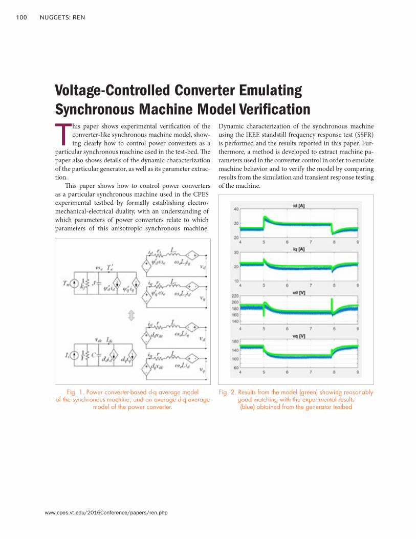
100
www.cpes.vt.edu/2016Conference/papers/ren.php
NUGGETS: REN
This paper shows experimental verification of the converter-like synchronous machine model, show-ing clearly how to control power converters as a
particular synchronous machine used in the test-bed. The paper also shows details of the dynamic characterization of the particular generator, as well as its parameter extrac-tion.
This paper shows how to control power converters as a particular synchronous machine used in the CPES experimental testbed by formally establishing electro-mechanical-electrical duality, with an understanding of which parameters of power converters relate to which parameters of this anisotropic synchronous machine.
Dynamic characterization of the synchronous machine using the IEEE standstill frequency response test (SSFR) is performed and the results reported in this paper. Fur-thermore, a method is developed to extract machine pa-rameters used in the converter control in order to emulate machine behavior and to verify the model by comparing results from the simulation and transient response testing of the machine.
Voltage-Controlled Converter Emulating Synchronous Machine Model Verification
Fig. 1. Power converter-based d-q average model of the synchronous machine, and an average d-q average
model of the power converter.
Fig. 2. Results from the model (green) showing reasonably good matching with the experimental results (blue) obtained from the generator testbed

101CPES ANNUAL REPORT 2016
www.cpes.vt.edu/2016Conference/papers/ren.php
The growing use of renewable energy sources, like wind and solar, has been growing increasingly, which has not only diversified the power generation
portfolio but also resulted in a paradigm shift in the way electricity is generated, transmitted, and consumed. With the help of power electronics, more and more distributed generation (DG) units are being installed very close to lo-cal consumption in medium- to low-voltage distribution power systems. The issues of the converter grid synchro-nization instability and the corresponding low-frequency power oscillations have been noticed by industry. The in-stability of doubly-fed induction generators is found to be related to improper PLL parameters. The aim of this paper is to provide such a system analysis by decomposing a PLL into two feedback loops; namely, a “grid synchronization loop” and a “self-synchronization loop.” This paper focuses on how the PLL dynamics, normally in the low-frequency region, are affected when the impedances of the grid and local loads change.
Fig. 1 shows the proposed PLL model considering the operation of the converter system. It is found that the ef-fect of this self-synchronization feedback is determined by φC, IC, and KC. Higher injection current, bigger grid input impedance, and bigger reactive components (big-ger φC) give a stronger self-synchronization feedback ef-fect. In addition, the resonant fre-quency ωr is one of the PLL equilibri-um points under is-landed conditions. The corresponding linearized small-signal model shows that when the is-landing condition
occurs, the PLL output tends to approach ωr and to stay at ωr even with a perturbation.
It is also found that the “self-synchronization” feed-back in the proposed model tends to drive the PLL output out of the steady state, and the loop characteristics greatly rely on multiple system parameters. The unstable nonlin-ear PLL output under the weak grid can be well predicted by the proposed model. A small-signal model under is-landing conditions, derived from the quasi-static PLL model, clearly explains the LHP and RHP pole character-istics for parallel RLC and series RLC loads. Both simula-tion and experimental results have validated the proposed model, as shown in Fig. 2.
Analysis of Phase-Locked Loop Low-Frequency Stability in Three-Phase Grid-Connected Power Converters Considering Impedance Interactions
Fig. 1. Quasi-static PLL model by considering converter interaction with the grid.
Fig. 2. (a) PLL output under //RLLL load condition: phase voltage vCa(bottom) [100 V/div] and ωC (top) [5 Hz/div].
(b) PLL output under //RLCLLL load condition: phase voltage vCa (bottom) [100 V/div] and ωC (top) [5 Hz/div].
(b)(a)

102
www.cpes.vt.edu/2016Conference/papers/ren.php
NUGGETS: REN
The modular multilevel converter (MMC) is a re-cently introduced converter topology with the potential for use with high-voltage direct current
(HVDC) for transmission and motor drive applications. One of the disadvantages of MMCs is that large capaci-tors are required to deal with the voltage ripple in the modules. In many papers, multiple control strategies were introduced to reduce the capacitor voltage ripple. One of the most effective methods is injecting circulat-
ing current to eliminate the power of second-order har-monics in sub-modules. Recently, a new method has been introduced that can eliminate the fundamental power of sub-modules by changing modulation index M. The state trajectory can offer us a clear view in order to analyze the working condition of every control method.
In simple duty cycle control law, the duty cycle is set in order to produce a purely sinusoidal output. The loop size of Fig 1 (a) represents the upper module output energy in one line cycle. That energy is the dominant reason for the capacitor voltage ripple. In Fig. 1 (b), the right-hand side shows the power transfer of the upper and lower arm modules. The relationship of upper module capaci-tor voltage vc1 and lower module capacitor voltage vc2 varies in the α axis and β axis. The α axis represent energy swapping between the upper and lower modules. The β axis represents energy transfer with the load and source simultaneously. The state trajectory is a result of the com-
bined effects of both axes.In order to reduce capacitor voltage ripple, a second-
order circulating current can be injected to eliminate the second-order power of the module. The second-order power of the module transfers only from the module to the load and source. In state trajectory, this power affects only the β axis. When the second-order harmonic power of the module is reduced to zero, the state trajectory of vc1 and vc2 should have no distance on the β axis. As Fig. 2(b) shows, the state trajectory is shaped only by the α axis. This means the only reason for the capacitor volt-age ripple is the energy swapping between the upper and lower modules.
Recently, a new method has been introduced to fur-ther reduce the capacitor voltage ripple which is based on the previous second-order current injection method. By adjusting a proper modulation index M, the fundamental power of the module can be significantly reduced. In the state trajectory, as shown in Fig. 3, the trajectory in the α axis was reduced to almost zero. This means that the module transfer between the modules was reduced.
By observing the state trajectory, we can get a visual representation of the module power transfer. State trajec-tory was a good tool for power analysis of the MMC and a good comparison method for different capacitor volt-age ripple reduction strategies.
State Trajectory Analysis of Modular Multilevel Converter
Fig. 1. State trajectory with simple control law.
Fig. 2. State trajectory with second-order harmonic circulating current injection.
Fig. 3. State trajectory with second-order current injection and modulation index adjusting.

103CPES ANNUAL REPORT 2016
www.cpes.vt.edu/2016Conference/papers/ren.php
To address the generation uncertainty problems in-troduced by renewable energy power plants, STAT-COMs are typically used to smoothen the point of
common coupling (PCC) voltage in order to facilitate the integration of the renewable energy into the grid. A con-
trol method has been proposed recently, the virtual syn-chronous machine (VSM), which controls grid-interfaced inverters to behave like synchronous machines so as to be more compatible with the existing power grid. These VSMs have been applied to STATCOMs and show an im-proved performance over conventional D-Q frame-based STATCOMs, along with tunable parameters that can be adjusted to different scenarios. In this paper, the concept is extended to a realistic STATCOM with an LCL filter, as Fig.1 shows, to mitigate harmonics as well as some practi-cal concerns about the active power compensation during transients, which is introduced by the VSM control meth-od shown in Fig. 2. A detailed small-signal design process is provided to guide the selection of virtual parameters and tuning of compensators. The performance is compared with conventional DQ-frame PLL-oriented STATCOM in both the frequency and time domains and shows bet-ter voltage regulation capability when there is frequency fluctuation in the power grid. A scaled-down prototype STATCOM, shown in Fig. 3, is constructed to validate the control schemes.
Design, Analysis and Experimental Evaluation of a Virtual-Synchronous-Machine-Based STATCOM with LCL Filter
Fig. 1. Circuit schematics of studied system.
Fig. 2. Control diagram of VSM-based STATCOM. Fig. 3. Prototype STATCOM.
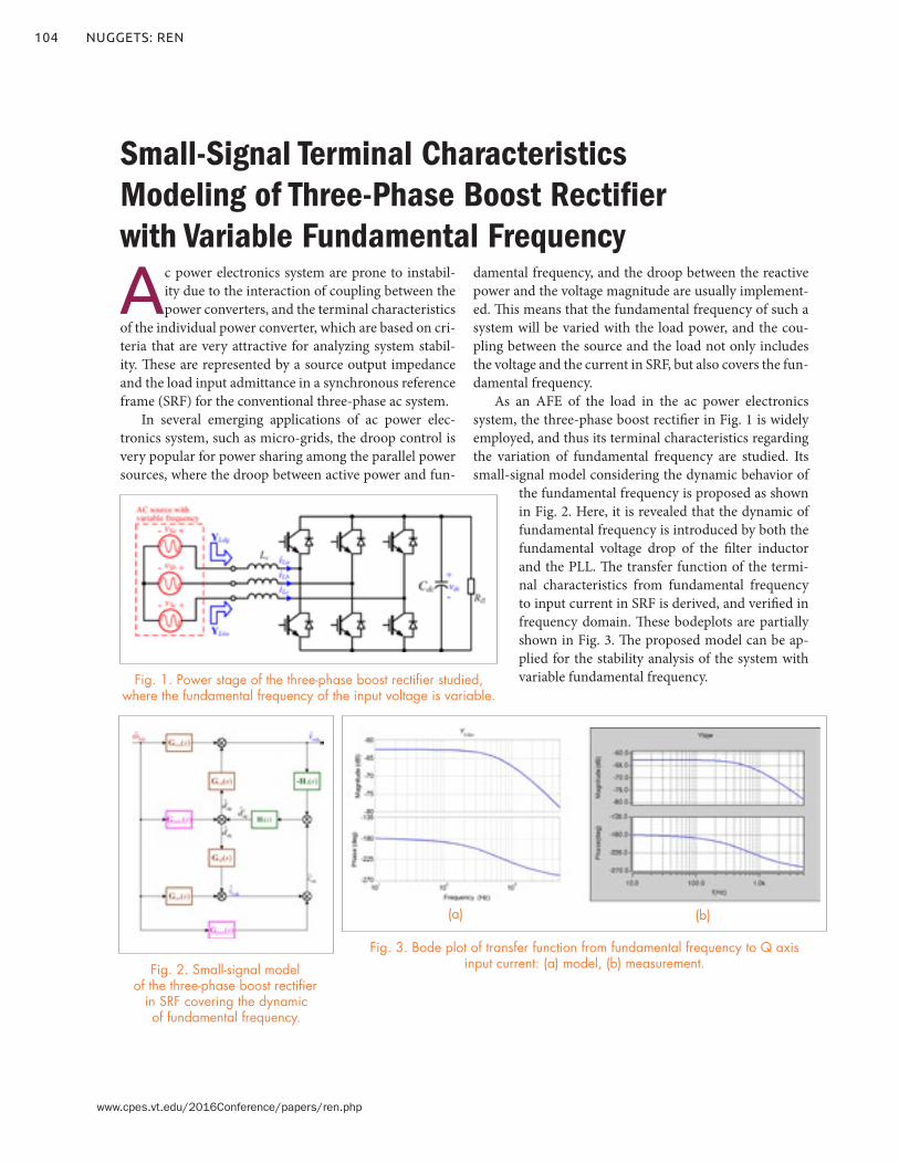
104
www.cpes.vt.edu/2016Conference/papers/ren.php
NUGGETS: REN
Ac power electronics system are prone to instabil-ity due to the interaction of coupling between the power converters, and the terminal characteristics
of the individual power converter, which are based on cri-teria that are very attractive for analyzing system stabil-ity. These are represented by a source output impedance and the load input admittance in a synchronous reference frame (SRF) for the conventional three-phase ac system.
In several emerging applications of ac power elec-tronics system, such as micro-grids, the droop control is very popular for power sharing among the parallel power sources, where the droop between active power and fun-
damental frequency, and the droop between the reactive power and the voltage magnitude are usually implement-ed. This means that the fundamental frequency of such a system will be varied with the load power, and the cou-pling between the source and the load not only includes the voltage and the current in SRF, but also covers the fun-damental frequency.
As an AFE of the load in the ac power electronics system, the three-phase boost rectifier in Fig. 1 is widely employed, and thus its terminal characteristics regarding the variation of fundamental frequency are studied. Its small-signal model considering the dynamic behavior of
the fundamental frequency is proposed as shown in Fig. 2. Here, it is revealed that the dynamic of fundamental frequency is introduced by both the fundamental voltage drop of the filter inductor and the PLL. The transfer function of the termi-nal characteristics from fundamental frequency to input current in SRF is derived, and verified in frequency domain. These bodeplots are partially shown in Fig. 3. The proposed model can be ap-plied for the stability analysis of the system with variable fundamental frequency.
Small-Signal Terminal Characteristics Modeling of Three-Phase Boost Rectifier with Variable Fundamental Frequency
Fig. 1. Power stage of the three-phase boost rectifier studied, where the fundamental frequency of the input voltage is variable.
Fig. 2. Small-signal model of the three-phase boost rectifier
in SRF covering the dynamic of fundamental frequency.
Fig. 3. Bode plot of transfer function from fundamental frequency to Q axis input current: (a) model, (b) measurement.
(b)(a)

105CPES ANNUAL REPORT 2016
www.cpes.vt.edu/2016Conference/papers/ren.php
Loosely coupled inductors are applied to inductive power transfer (IPT) systems to replace the bulky cables and plugs used as the conventional charging
method for electric vehicles (EVs). By using proper com-pensation networks with capacitors, power can be trans-ferred through a distance of up to tens of centimeters. Advantages of the IPT system include convenience for drivers, safety when charging in a humid environment, and the potential for dynamic charging when vehicles are moving. Performances of inductive power transfer (IPT) systems are directly influenced by the coils parameters such as self-inductance, mutual inductance, and winding resistance.
However, the designed values of the above mentioned parameters for the IPT coils are not repeatable or opti-mized for different specifications, e.g. operating frequen-cy and load conditions, so the coil parameters need to be redesigned whenever the specifications are changed. To avoid such a redundant redesign process, normalized pa-rameters, including load quality factor, coil quality factor, and normalized operating frequency, are implemented in the design process of the IPT coils. The normalized parameters are independent of the specifications, so the design results can be used for different specifications. In this paper, a systematic design method is demonstrated for normalized parameters of coils in a series-series IPT system as in Fig. 1. The desired voltage gain, soft-switch-ing of the converter switches, and required coil efficiency are all achieved following this method.
To verify the normalized design method, coils with the dimensions of 250mm × 250mm and a 100mm air gap are designed for a 3.3kW IPT system. The experi-ment proves that the desired output voltage from 200V to 400V is achieved with a corresponding voltage gain from 0.5 to 1. The ZVS of the inverter devices is achieved because the inverter’s output current is lagging behind its output voltage. As required, coil efficiency is larger than 97%.
Normalized Design Method for Coils in Series-Series Inductive Power Transfer System
Fig. 1. Topology of series-series inductive power transfer system.
Fig. 2. Coils for experimental verification and its measurement results.

106
www.cpes.vt.edu/2016Conference/papers/ren.php
NUGGETS: REN
Modular Multilevel Converter (MMC) is an at-tractive solution for high-voltage, high-power applications. It can invert high direct current
(dc) voltage into high alternating current (ac) voltage without a transformer. In today’s MMC products, a rather large capacitor bank is employed in each module to sup-press low frequency (both fundamental and 2nd order) voltage ripple. With a detailed power analysis, a novel concept of over modulation is proposed to eliminate all low frequency power components in the module.
The structure of MMC is shown in Fig. 1. Each phase of MMC contains two arms, which consists of submod-ules and one arm inductor. The number of submodules can be an arbitrary value, N. The topology of the sub-module can be half bridge or full bridge. The arm cur-rent can contain harmonics beside dc and 1st order terms:
Under traditional control, the harmonic is suppressed, where modules offer 2nd power to the ac load besides a
1st order oscillating power between two arms. The capaci-tor voltage is shown in Fig. 2. To avoid the 2nd power in modules, a proper 2nd harmonic current can be injected in both arm currents, where the dc source would offer that 2nd power to the ac load and the oscillating power contains a dominated 1st order part and a small 3rd order part. The capacitor voltage is shown in Fig. 3.
The definition of modulation index is introduced for further power analysis, As a result, the module power can be rewritten as a function of M. The total upper arm power and lower arm power are:
When M=1.15, the significant 1st order power is also eliminated. Over modulation is realized with full bridge modules. The capacitor voltage is shown in Fig. 4.
Capacitor Voltage Ripple Reduction for Modular Multilevel Converter with 2nd Order Current Injection and Over Modulation
Fig. 1. MMC structure and module topologies.
Fig. 2. Cap. Voltage when ihar=0.
Fig. 3. Cap. Voltage when ihar=Idccos2ϖt.
Fig. 4. Cap. Voltage when ihar=Idccos2ϖt and M=1.15.

107CPES ANNUAL REPORT 2016
www.cpes.vt.edu/2016Conference/papers/ren.php
Multilevel converters are composed of series-con-nected semiconductors and can operate at higher voltages than the voltage rating of the individual
devices. These converters are divided into three main cate-gories: the neutral-point clamped capacitor (NPC), the fly-ing capacitor (FC) and the cascaded topologies, which it-self is divided into cascaded H-bridge (CHB) and cascaded half-bridge or the modular multilevel converter (MMC). Multilevel converters are of special interest in applications such as active front-end rectifiers (AFE), high-voltage direct-current transmission (HVDC), static compensators (STATCOM), high-power motor drive applications, bat-tery energy storage systems, and photovoltaic applications. The modular multilevel converter is the state-of-the-art converter among multilevel topologies and has received a huge amount of attention from researchers over past years.
In this paper, the particle swarm optimization (PSO) algorithm is used to calculate the optimal magnitude and phase angle of the circulating current components in or-der to minimize the voltage ripple across the capacitors. The 2nd and 4th harmonic components of the circulating current are considered to minimize the voltage ripple. The approach is based on an average model derived for the converter. For different magnitudes of arm induc-tance (representing different applications such as motor drives and AFEs.) the capacitor voltage waveforms are compared with the natural circulating current, eliminat-ing the circulating current and when injecting an optimal magnitude of the circulating current. Also, the effect of the circulating current on the efficiency of the converter is investigated by calculating the semiconductor losses.
Analysis of Capacitor Voltage Ripple Minimization in Modular Multilevel Converter Based on Average Model
Fig. 1. (a) MMC inverter and (b) Half-bridge submodule as building-block of MMC converter.

108
www.cpes.vt.edu/2016Conference/papers/ren.php
NUGGETS: REN
Passive components are one of the major factors af-fecting the cost, volume and weight of power elec-tronic systems. The three-level converter has been
proposed for use in high-dc-voltage applications because of its low switching voltage stress and smaller passive component size. For high-current applications, convert-ers paralleled with interleaving operation can be applied to reduce the input and output passive component size. For paralleled three-level converters, inversely-coupled inductors are essential to reduce the circulating current between the interleaved two phases. Inversely-coupled inductors also suppress the current ripple in each phase while keeping the benefits of interleaving, such as a low output current ripple and low common-mode voltage.
In this work, a new design is proposed to integrate the two coupled inductors as one magnetic component. The schematic is shown in Fig. 1(a), where the inductors to be integrated are shown in the red box. The concept drawing of the new structure is shown in Fig. 1(b). This integrated inductor can achieve the purpose of suppress-ing circulating current and boosting output inductance at the same time.
With high-frequency operation, amorphous and nanocrystalline materials are good candidates for the magnetic core due to their low core loss and high satura-tion. These two types of materials are usually produced in the form of a tape-wound core, so the flux must flow in the direction of the lamination layers. The structure in Fig. 2(a) is proposed to realize the concept drawing of Fig. 1(b). Fig. 2(b) shows the different flux paths for dif-ferent parts of the core.
After calculating the required output inductances to minimize switching loss and output capacitor size, the different mutual inductances can be calculated. This cor-responds to a certain flux in each leg, which is divided into two components; the BCM is a large dc flux with a very small ripple, and the BDM is a large-amplitude ac flux. These two flux components have to be limited to a certain range determined by the allowable saturation level in each leg and the generated core loss.
To optimize the core size and weight, the product of N (number of turns) and Ae (equivalent core cross-section area) should be minimized with the previously mentioned constraints. A design procedure is proposed
in this work, with two material candidates for high-power applications; iron-based Amorphous has a higher satura-tion limit (1.56T, Metglas®2605SA1), while Nano-crytal-line has lower core loss but a lower saturation limit (1.2T, FINEMET®). Fig. 3 shows the N × Ae variation for the two materials with different operating voltages and currents with a fixed inductance, operation frequency and duty ra-tio. From this we can conclude that minimizing the size of the core is not only dependent on the material but also on the operating parameters of the converter.
Magnetic Material Selection Procedure for a Coupled Inductor used in Interleaved Three-level Multi-phase DC-DC Converters
Fig. 1. (a) Three-level dc-dc converter with integrated coupled inductor (b) Integrated core structure
(concept drawing).
Fig. 2. (a) Integrated structure with tape-wound core (b) Exploded view: Flux path in the coupled inductor.
Fig. 3. Comparison of amorphous and nano-crystalline materials.

109CPES ANNUAL REPORT 2016
www.cpes.vt.edu/2016Conference/papers/ren.php
This paper investigates using a multi-phase three-level dc-dc converter for high-power, high-voltage renewable energy systems. With interleaving mod-
ulation and coupled inductors, both the inductor current ripple and output current ripple are largely reduced com-pared with traditional non-interleaving, single inductor architectures. To improve power density, coupled induc-tors are further integrated. The small-signal model of the converter with integrated coupled inductors is compared with the conventional buck converter to show their simi-larities. In addition, magnetic design is discussed based on magnetic circuit analysis and different magnetic material selection.
With one integrated coupled inductor, as shown in Fig. 1, the power density can be in-creased to be higher than the conventional solution of two coupled inductors. Based on the small-signal model of the three-terminal switch, the small-signal model of the converter is derived in Fig. 2. The result indicates that the integrated coupled inductors can be decoupled during transient response, assuming it is a symmetrical structure. Comparing this with a conventional buck converter, it is obvious that the only difference is the equivalent inductance, 4Mac+Llk. In other words, only the positive coupling mutual induc-tance and the leakage inductance determine the small-signal characteristics. The negative coupling between arms a and b and between arms c and d is designed to suppressed the circulating current in the converter and reduce the inductor current ripple.
To fully understand the integrated coupled inductors and provide guidance for design, the flux is separated into a common-mode part and differential-mode part in the magnetic circuit, as shown in Fig. 3. In this diagram, the red curve represents the negative coupled flux (DM flux) between arms a and b and between arms c and d. The green curve (CM flux) represents the positive coupled flux among the four arms. The analysis of this magnetic
circuit indicates that the negative coupled flux is pure large ac ripple, and related to the tolerable core loss den-sity. The positive coupled flux is a large dc flux plus a very small ripple and directly determined by the output cur-rent, which indicates that there would be a potential core saturation problem under certain working conditions if it is not properly designed. There will be trade-offs between core loss and saturation limitations for different magnetic materials of the core.
Study on Three-level DC-DC Converter with Coupled Inductors
Fig. 1. Three-level dc-dc converter with integrated coupled inductors.
Fig. 3. Magnetic circuit of integrated coupled inductors.
Fig. 2. Small-signal model of the converter.

110
www.cpes.vt.edu/2016Conference/papers/ren.php
NUGGETS: REN
The modular multilevel converter (MMC) has re-ceived increased attention due to its interesting features, such as inherent modularity, voltage and
current scalability, and easy assembly. While the MMC has the advantage of having a flexible converter design, the design still requires reliability, like any other system. Modeling and simulation are powerful tools in design-ing a converter. However, a fundamental disconnect of-ten exists between simulations and practical applications. Whereas most simulations are deterministic in nature, when engineering applications are steeped in uncertainty arising from a number of sources—such as those due to the manufacturing processes, natural material variabil-ity, initial conditions, wear or damaged conditions of the system, and the system surroundings—the modeling process itself can introduce huge uncertainties. These can be due to assumptions made during the process as well as the numerical approximations employed in the simu-lations. Therefore, design margins are conservatively es-timated using a heuristic factor of safety to compensate for the deviation of real system behavior from simulation results when using modeling and simulation in converter design.
In this paper, a new approach is proposed in which different sources of uncertainties that cause the mis-match between modeling and simulation predictions and real system behavior are identified and characterized so that they can be predicted ahead of time to eliminate the use of large safety margins (shown in Fig. 2). Using this approach, modeling and simulation results can be used during the early design stages with confidence in their predictive proficiency and accuracy.
In the first section, an overview of the verification, validation, and uncertainty quantification (VV&UQ) process is described as enabling us to identify, charac-terize and quantify different sources of uncertainties in modeling, simulation, and experiment. In the second section, the concept from the first section is employed
to calculate and minimize the required design margins by using probabilistic modeling and simulation. To this end, the peak voltage across the semiconductor device in an MMC (shown in Fig. 1)—which is a key variable used to size the capacitor bank—is selected as an example to il-lustrate the methodology proposed in this paper.
Model-Based Design of a Modular Multilevel Converter with Minimized Design Margins
Fig. 1. Circuit configuration of a modular multilevel converter.
Fig. 2. Final probability box of maximum voltage a cross semiconductor device indicating total uncertainty.

111CPES ANNUAL REPORT 2016
www.cpes.vt.edu/2016Conference/papers/ren.php
It has been shown that the small-signal stability of dc power systems can be determined by analyzing the output impedance of the source and the input imped-
ance of the load using an impedance criterion such as the Middlebrook Criterion. To generate a higher power per-turbation in order to extract the impedances at any de-sired interface, a dedicated injection device is preferred. This paper describes the design and implementation of such an impedance measurement unit (IMU) suitable for in-situ impedance measurement in a MVDC system.
For accurate measurement of both source and load side impedances, the PIU should be able to inject both current in shunt and voltage in series. When in shunt current injection mode, the PIU need to stand full system voltage and inject only a few percent of system current. When in series voltage injection mode, the PIU conducts full system current while injecting only a few percent of the system voltage. A Power Electronics Build-ing Block (PEBB)-based converter is designed for this ap-plication. The PEBBs are reconfigured in shunt and series injection modes to serve the two very different ratings, as shown in Fig. 1.
The control block diagram of a shunt current injection mode (in Fig. 2 (a)) and a series voltage injection are giv-en. A fast current loop with a 3kHz bandwidth is designed to achieve good tracking of the perturation reference sig-
nal. The current reference is the sum of the two parts: per-turbation reference and output of dc bus voltage control loop, which is designed to have sub-hertz bandwidth so as to not interfere with the perturbation reference. In ad-dition, there is a dc voltage balancing controller designed to deal with the component parameter difference between each PEBB, such as dc capacitance and operation loss. The external loop controls (Fig. 2 (b)) the voltage across the capacitor, which has two parts. One is the perturba-tion voltage reference given by the upper level control. The other is the output of dc bus voltage controller.
Small-Signal Impedance Measurement in Medium-Voltage dc Power Systems
Fig. 1. Medium-voltage IMU prototype.
vcf
d1
ilf1
vcf
vcf
d2
d3
ilf2
ilf3
vdc1
vdc2
vdc3
Cvcf(s)
vcf isys
1/3
Cbal(s)vdcavg
vdc1
-Δvdc1
vdcavg
vdc2
-Δvdc2
Δilfref1
Δilfref2
Cvdc(s)vdcref
vdcavg
Δilfref3
ilfref
ilfref1
ilfref2
ilfref3
Cbal(s)
Cilf1(s)
Cilf2(s)
Cilf3(s)
vdc2vdc1 vdc3
vper
Fig. 2. Control diagram of (a) shunt current injection mode, (b) shunt series voltage injection mode.
(a) (b)
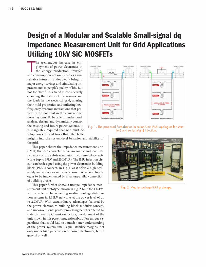
112
www.cpes.vt.edu/2016Conference/papers/ren.php
NUGGETS: REN
The tremendous increase in em-ployment of power electronics in the energy production, transfer,
and consumption not only enables a sus-tainable future, it undoubtedly brings a major energy savings and stimulating im-provements to people’s quality of life. But not for “free.” This trend is considerably changing the nature of the sources and the loads in the electrical grid, altering their mild properties, and inflicting low-frequency dynamic interactions that pre-viously did not exist in the conventional power system. To be able to understand, analyze, design, and dynamically control the existing and future power systems, it is inarguably required that one must de-velop concepts and tools that offer better insights into the system-level behavior and stability of the grid.
This paper shows the impedance measurement unit (IMU) that can characterize in-situ source and load im-pedances of the sub-transmission medium-voltage net-works (up to 69kV and 250MVA). The IMU injection cir-cuit can be designed using the power electronics building block (PEBB) concept, in Fig. 1, as it offers a high-scal-ability and allows for numerous power conversion topol-ogies to be implemented by a series/parallel connection of building blocks.
This paper further shows a unique impedance mea-surement unit prototype, shown in Fig. 2, built for 4.16kV, and capable of characterizing medium-voltage distribu-tion systems in 4.16kV networks at the power level of up to 2.2MVA. With extraordinary advantages featured by the power electronics building block modular concept, and unconventional power processing benefits offered by state-of-the-art SiC semiconductors, development of the unit shown in this paper unquestionably offers unique ca-pabilities that could lead to a much better understanding of the power system small-signal stability margins, not only under high penetration of power electronics, but in general as well.
Design of a Modular and Scalable Small-signal dq Impedance Measurement Unit for Grid Applications Utilizing 10kV SiC MOSFETs
Fig. 2. Medium-voltage IMU prototype.
Fig. 1. The proposed Perturbation Injection Unit (PIU) topologies for shunt (left) and series (right) injection.

113CPES ANNUAL REPORT 2016
www.cpes.vt.edu/2016Conference/papers/ren.php
Due to environmental problems caused by fossil fuels and sustainable development challenges, worldwide installation of photovoltaic (PV) systems is increas-
ing exponentially. According to solar energy industries as-sociation (SEIA), U.S. PV installations increased more than 50% annually from 2009 to 2013. A dominant part of these installations is the PV farm, but commercial (>10kW) and residential (2-10kW) PV generators are also increasing rapidly, making their total installations comparable to PV farms. There will be high PV penetration in the distribu-tion system as well as in the transmission system.
Such a significant energy supply change may have a re-markable effect on the static and dynamic performance of the distribution system. Impacts of PV injection include voltage profile changes due to solar generator output in-termittency, and a power loss increase caused by varied power flow. Much research has been done to assess these static problems in distribution systems, but most papers assume that no reactive power is produced by PV invert-ers. However, according to the revised IEEE 1547 stan-dard, distribution resources can actively participate to regulate the voltage by changes of real and reactive power. This paper develops a static model considering three dif-
ferent reactive power operation modes of PV generators and applies the model in a medium voltage distribution feeder. According to the Jacobian matrix of power flow equations, sensitivity indices of voltage or power loss in-crease over solar power input are calculated, to quantify the impact of PV injection at different locations, different capacities and different reactive power operation modes.
A steady state model is proposed for the PV generator working at different reactive power operation modes, and the sensitivity matrix for voltage increase over solar active power is defined using a Jacobian matrix deducted from the power flow equations, depending on which sensitiv-ity index for system power loss over solar active power is built. The sensitivity matrix and index for a 12kV radial distribution system case are calculated by MATLAB, and proven to be accurate by simulation results in PSS/E. The sensitivity matrix and index can be used to analyze the impact of PV injection on bus voltages within the whole system and system power loss. For the selected distribu-tion system, more active power can be injected when the PV generator is working on mode 3 and PV generators working on mode 2 will increase power system loss more rapidly.
Assessment of Medium Voltage Distribution Feeders under High Penetration of PV Generation
Fig. 1. One line diagram of the distribution system.Fig. 2. System voltage contour after 1.36MW
injected at bus 19.

114
www.cpes.vt.edu/2016Conference/papers/ren.php
NUGGETS: REN
In distributed power system (DPS), as shown in Fig.1, one converter's switching frequency ripples are another converter's perturbations and beat frequency oscil-
lations may be generated due to the power converter’s nonlinearities. This paper proposes an extended multi-frequency output impedance model to describe the non-linearities of power converters and to analyze the high frequency interactions of DPS.
The voltage mode controlled boost converter is specifically illustrated as a demonstration. For a volt-age mode controlled boost converter, the switches and PWM comparator generate multiple sidebands in the frequency domain. Therefore, with a sinusoidal current perturbation frequency excitation, the output voltage response contains not only the perturbation frequency, but also multiple sidebands and these sidebands can be reordered from low to high and written as, and
This work develops the relationship between output current perturbation and output voltage perturbation at both perturbation frequency and sideband frequencies (we define this relationship as extended output imped-ance). The frequency characteristics around switching frequency are shown in Fig. 2. Here, the figure shows that the switching frequency is a very important parameter for output impedance characteristics. Although its varia-tion has almost no effect on traditional impedance char-acteristics, it affects the relationship between the output voltage’s sidebands and the output current perturbation such as
The high-frequency interaction analysis for DPS shown in Fig.1 is based on the proposed model. If the switching frequency of one converter is 20kHz while that of another is 19.5kHz, the interaction of switching frequency ripples will produce multiple sidebands. Ac-cording to the proposed model (as shown in Fig. 2), if the low-frequency component takes a much larger gain than that of other components, including the perturbation frequency 19.5kHz itself, then there will be a 500Hz oscillation in the bus voltage. The simulation re-sult is shown in Fig. 3. However, if the two converters’ switching frequencies are both 20kHz, from Fig. 2, there will be no oscillations in the bus voltage. The simulation result for this case is shown in Fig. 4.
Therefore, when designing power converters used for DPS, it should be suggested that the switching frequen-cies be checked and optimized by the proposed method to improve the power quality.
Modeling and Analysis of High Frequency Interactions for Distributed Power System
).(
Fig.1. Switching frequency ripples’ interaction.
Fig. 2. Output frequency characteristics around switching frequency.
Time(s)0.03 0.032 0.034 0.036 0.038 0.04
23.4
23.6
23.8
24
24.2
24.4
24.6
Bus Voltage Waveform
Time(s)0.03 0.032 0.034 0.036 0.038 0.04
23.4
23.6
23.8
24
24.2
24.4
24.6
Bus Voltage Waveform
20kHz-19.5kHz=500Hz
Volta
ge(V
)Vo
ltage
(V)
Fig. 3. Fig. 3 Switching frequencies are both 20kHz.Time(s)
0.03 0.032 0.034 0.036 0.038 0.0423.4
23.6
23.8
24
24.2
24.4
24.6
Bus Voltage Waveform
Time(s)0.03 0.032 0.034 0.036 0.038 0.04
23.4
23.6
23.8
24
24.2
24.4
24.6
Bus Voltage Waveform
20kHz-19.5kHz=500Hz
Volta
ge(V
)Vo
ltage
(V)
Fig. 4. Switching frequencies are 19.5 and 20kHz.
)(
.

Sponsored Research NuggetsEMI Filter Design of DC-Fed Motor-Drives Using Behavioral EMI Models
Energy-Harvesting Shock Absorbers with Riding Comfort controller on Vehicle Sus-pension Systems
Gate Driver with Overshoot Regulation and Active Snubbing
Modeling of Plate-Core Inductors and Coupled Inductors
A 50 kW SiC Three-Phase AC-DC Convert-er Design for High Temperature Operation
High-Density, Fast-Switching 1.2 kV, 90 A Diode-Less SiC MOSFET Half-Bridge Module and Gate Drive Design
Design of a High-Density, Diode-Less 1.2 kV, 90 A SiC MOSFET Half-Bridge Power Module
Advances in SiC-Based Power Conversion for Shipboard Electrical Power Systems
Point-of-Load Inductor with High Swinging and Low Loss at Light Load
Very High Frequency Integrated VR for Small Portable Devices
Magnetic Characterization Technique and Materials Comparison for Very High Frequency IVR
Wide-bandwidth Identification of Small-Signal dq Impedances of ac Power Systems via Single-Phase Series Voltage Injection
A Novel High Efficiency System Architec-ture for Bi-directional On Board Battery Charger
High Frequency PCB Winding Transformer Design for On Board Battery Charger
Wide Range and High Power Density GaN-Based DC-DC Converter Design
High-Frequency CRM AC/DC Converter for WBG-Based 6.6kW On-Board Charger
Dynamic Sharing Between Paralleled SiC MOSFETs Caused by Threshold Voltage Mismatch
Spurious Turn-On inside a Power Module of Paralleled SiC MOSFETs
Testing of a Novel Medium Voltage Imped-ance Measurement Unit
Differential-mode EMI emission predic-tion of SiC-based power converters using a mixed-mode unterminated behavioral model
Gate Driver Design for 1.7kV SiC MOSFET Module with Rogowski Current Sensor for Shortcircuit Protection
Design and Optimization of a High Per-formance Isolated Three Phase AC/DC Converter
Small-Signal Stability Analysis of Three-Phase AC Systems in the Presence of Constant Power Loads Based on Mea-sured d-q Frame Impedances
Effect of Heating Rate on Bonding Strength of Pressure-free Sintered Nanosilver Joint
Driving and sensing design of an enhancement-mode-GaN phase-leg as a building block
Inductor Coupling and Integration for 6.6kW On Board Battery Charger
DC Fault Control of Modular Multilevel Converter with Full-Bridge Cells
High Density Integration of High Fre-quency High Current Point-of-Load (POL) Modules with Planar Inductors
115CPES ANNUAL REPORT 2016
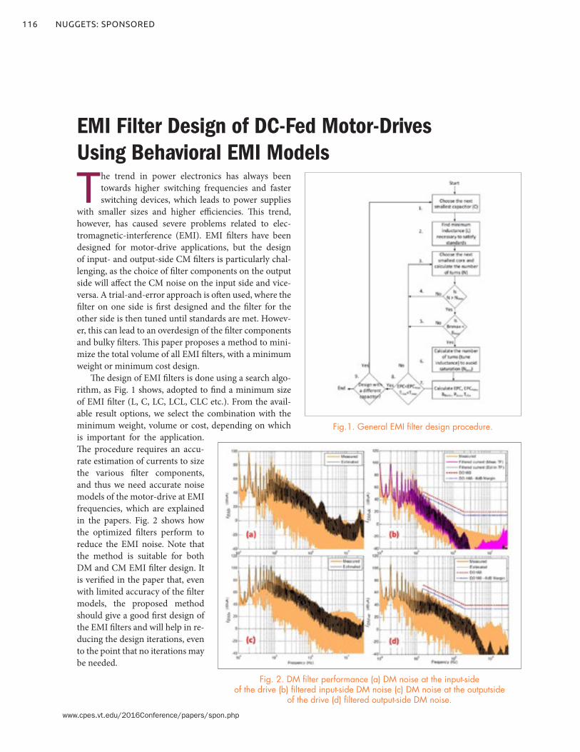
116
www.cpes.vt.edu/2016Conference/papers/spon.php
NUGGETS: SPONSORED
The trend in power electronics has always been towards higher switching frequencies and faster switching devices, which leads to power supplies
with smaller sizes and higher efficiencies. This trend, however, has caused severe problems related to elec-tromagnetic-interference (EMI). EMI filters have been designed for motor-drive applications, but the design of input- and output-side CM filters is particularly chal-lenging, as the choice of filter components on the output side will affect the CM noise on the input side and vice-versa. A trial-and-error approach is often used, where the filter on one side is first designed and the filter for the other side is then tuned until standards are met. Howev-er, this can lead to an overdesign of the filter components and bulky filters. This paper proposes a method to mini-mize the total volume of all EMI filters, with a minimum weight or minimum cost design.
The design of EMI filters is done using a search algo-rithm, as Fig. 1 shows, adopted to find a minimum size of EMI filter (L, C, LC, LCL, CLC etc.). From the avail-able result options, we select the combination with the minimum weight, volume or cost, depending on which is important for the application. The procedure requires an accu-rate estimation of currents to size the various filter components, and thus we need accurate noise models of the motor-drive at EMI frequencies, which are explained in the papers. Fig. 2 shows how the optimized filters perform to reduce the EMI noise. Note that the method is suitable for both DM and CM EMI filter design. It is verified in the paper that, even with limited accuracy of the filter models, the proposed method should give a good first design of the EMI filters and will help in re-ducing the design iterations, even to the point that no iterations may be needed.
EMI Filter Design of DC-Fed Motor-Drives Using Behavioral EMI Models
Fig.1. General EMI filter design procedure.
Fig. 2. DM filter performance (a) DM noise at the input-side of the drive (b) filtered input-side DM noise (c) DM noise at the outputside
of the drive (d) filtered output-side DM noise.

117CPES ANNUAL REPORT 2016
www.cpes.vt.edu/2016Conference/papers/spon.php
The input current/force of the mechanical-motion rectifier (MMR) can be controlled by using the con-troller proposed by this paper, and a better passenger
experience can be provided with a high-efficiency energy-harvesting suspension system. The nonlinear character-istics from one-way clutches and inertia in MMR induce disengagement and require a large equivalent capacitor, which makes the input current/force of the MMR uncon-trollable with a conventional feedback controller design. The controller that has been used in continuous, linear systems cannot be applied in an MMR system. This pa-per presents an input current/force tracking (ICFT) con-troller for MMR-based suspension systems. Additional control laws are added in the conventional controller to address the problem of nonlinearity during MMR con-trol. The input current/force of the MMR is controlled to follow the reference signal from the skyhook. The ve-hicle body displacement is tested by a speedbump on the ground. The displacement error between the skyhook and the ICFT-MMR is within 5%. The total harvested energy is 56 joules, as 56W of average input power. Equivalent cir-cuits are proven to have identical performances as me-chanical models.
In this work, a high-efficiency and reliable energy-harvester–the MMR–is adopted as both an energy har-vester and a semi-active shock absorber. To control the regenerative shock absorber, a mechanical-electrical equivalent circuit of the MMR is first introduced. Then an equivalent circuit of a quarter-car model with a sky-hook controller (one of the riding comfort controllers) is developed. Next, based on these equivalent circuits, an input current/force tracking controller is proposed and implemented on full-bridge power converter. As a result, the MMR’s force can be controlled under its nonlinear and discontinuous characteristics. The controller is con-structed based on pulse-width modulation (PWM) con-trol in a power converter, which also functions as an ac-dc converter transferring the energy to the battery. The controller is tested by tracking the reference force from skyhook control to improve riding comfort
The energy harvesting capability tested in Fig. 3 shows that total harvested energy Ein from the speedbump will
be around 56 joules, from which the mean harvested power Pin can be calculated as 56W. Moreover, better rid-ing comfort can be achieved by dynamic controls based on the ICFT controller.
Energy-Harvesting Shock Absorbers with Riding Comfort controller on Vehicle Suspension Systems
Fig. 1. Quarter car model with mechanical-motion rectifier (MMR) and power converter:
(a) Mechanical diagram of suspension system with MMR; (b) Mechanical structure of MMR.
Fig. 2. Input current/force tracking (ICFT) MMR-based suspension system using control laws
Fig. 3. Impulse response of power converter’s input power (Pin) and total harvested energy (Ein).
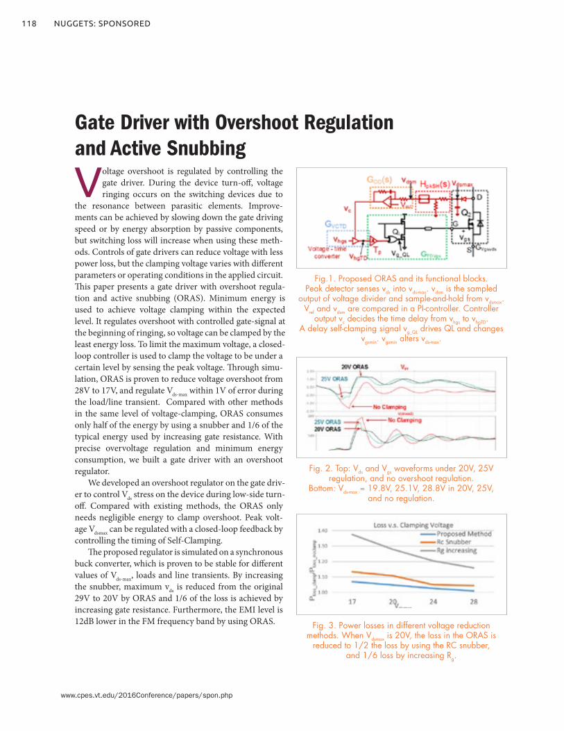
118
www.cpes.vt.edu/2016Conference/papers/spon.php
NUGGETS: SPONSORED
Voltage overshoot is regulated by controlling the gate driver. During the device turn-off, voltage ringing occurs on the switching devices due to
the resonance between parasitic elements. Improve-ments can be achieved by slowing down the gate driving speed or by energy absorption by passive components, but switching loss will increase when using these meth-ods. Controls of gate drivers can reduce voltage with less power loss, but the clamping voltage varies with different parameters or operating conditions in the applied circuit. This paper presents a gate driver with overshoot regula-tion and active snubbing (ORAS). Minimum energy is used to achieve voltage clamping within the expected level. It regulates overshoot with controlled gate-signal at the beginning of ringing, so voltage can be clamped by the least energy loss. To limit the maximum voltage, a closed-loop controller is used to clamp the voltage to be under a certain level by sensing the peak voltage. Through simu-lation, ORAS is proven to reduce voltage overshoot from 28V to 17V, and regulate Vds-max within 1V of error during the load/line transient. Compared with other methods in the same level of voltage-clamping, ORAS consumes only half of the energy by using a snubber and 1/6 of the typical energy used by increasing gate resistance. With precise overvoltage regulation and minimum energy consumption, we built a gate driver with an overshoot regulator.
We developed an overshoot regulator on the gate driv-er to control Vds stress on the device during low-side turn-off. Compared with existing methods, the ORAS only needs negligible energy to clamp overshoot. Peak volt-age Vdsmax can be regulated with a closed-loop feedback by controlling the timing of Self-Clamping.
The proposed regulator is simulated on a synchronous buck converter, which is proven to be stable for different values of Vds-max, loads and line transients. By increasing the snubber, maximum vds is reduced from the original 29V to 20V by ORAS and 1/6 of the loss is achieved by increasing gate resistance. Furthermore, the EMI level is 12dB lower in the FM frequency band by using ORAS.
Gate Driver with Overshoot Regulation and Active Snubbing
Fig.1. Proposed ORAS and its functional blocks. Peak detector senses vds into vds-max. vdsm is the sampled
output of voltage divider and sample-and-hold from vdsmax. Vref and vdsm are compared in a PI-controller. Controller
output vc decides the time delay from vhgs to vhgTD. A delay self-clamping signal vg_QL drives QL and changes
vgsmin. vgsmin alters vds-max.
Fig. 2. Top: Vds and Vgs waveforms under 20V, 25V regulation, and no overshoot regulation.
Bottom: Vds-max = 19.8V, 25.1V, 28.8V in 20V, 25V, and no regulation.
Fig. 3. Power losses in different voltage reduction methods. When Vdsmax is 20V, the loss in the ORAS is
reduced to 1/2 the loss by using the RC snubber, and 1/6 loss by increasing Rg.

119CPES ANNUAL REPORT 2016
www.cpes.vt.edu/2016Conference/papers/spon.php
Planar magnetics are widely used in bias power sup-plies for the benefits of their low profile and their compatibility with printed-circuit boards (PCB).
This paper studies the inductors and coupled inductors with winding layers sandwiched between two core plates (see Fig. 1) to model self-inductance, winding loss, core loss, and leakage inductance. The most challenging task for the plate-core inductor is to model the magnetic field with finite core dimensions, very non-uniform flux pattern, and large fringing flux.
Motivated by the finite-element analysis (FEA) plot of flux lines, a proportional-reluctance, equal-flux (PREF) model is developed to find the magnetic field by divid-ing the reluctance into several tubes that carry the same amount of flux. The methodology to construct the tubes is given, and the ratio of the magnetic field versus space is found from the ratio of the flux over the cross-section-al areas. The inductance, ac winding loss, core loss, and
leakage inductance are derived based on the modeling re-sult of the field. Prototypes made of a flexible circuit for single-winding inductors are tested with different layouts to verify the model.
Fig. 2 shows the modeled flux lines of a plate-core in-ductor with 16 turns. The flux in the core and the air gap can be modeled accurately based on the reluctance calcu-lation. The magnetic field found from the ratio of the flux over the cross-sectional area of the tubes matches very well with simulation results. The magnetizing inductance based on the field distribution is verified by both FEA and experimental results. A preliminary design procedure is delineated with an example for the specified magnetizing inductance and dc quality factor. The winding loss calcu-lated from the 2-D method is discussed, as are the errors caused by the cylindrical coordinates. The methodologies for core loss calculation and leakage inductance calcula-tion of coupled-inductors are also described.
Modeling of Plate-Core Inductors and Coupled Inductors
Fig. 1. 3D structure of plate-core coupled inductor with 5 × 5 mm2 footprint and 0.3mm core height.
Fig. 2. Flux lines from proportional-reluctance, equal-flux model.

120
www.cpes.vt.edu/2016Conference/papers/spon.php
NUGGETS: SPONSORED
The requirement for converters to operate in harsh environments has been a growing trend in indus-trial applications. This includes the automotive,
aerospace, oil and gas, and renewable energy industries. Wide bandgap materials such as silicon carbide (SiC) have demonstrated improved performance over silicon devices at elevated temperatures. SiC allows for simplified and less expensive cooling systems, higher efficiency, and increased power density. In addition to high-temperature (HT) semiconductors, the packaging materials, passive and control components, and gate drives must also be able to operate reliably in these harsh environments.
In this work, a 50kW three-phase ac-dc converter capable of 200° C-ambient operation was designed and tested (Fig. 1).
To meet the 50kW power requirement, each single phase-leg module in the converter should have a rating of at least 1200V and 100A. However, at the time, none of the commercially available high-power modules were designed for >150° C. This was mainly due to the temper-ature limitations of the packaging materials. Therefore, a customized 1200V, 120A SiC MOSFET phase-leg mod-ule was designed and fabricated with careful selection of the packaging materials to allow for operation in 200° C ambient environments. The module layout was also op-timized such that it could be utilized in high-frequency converters with a fast switching speed, while having min-imal device stresses.
To drive these modules, the HADES half-bridge iso-lated gate driver circuit from Cissoid was used. This gate driver can operate in 175° C ambient environments with short excursions up to 225° C. Other features include an isolated regulated power supply, 4A peak output current, 30kV/µs typical transient immunity, under-voltage lock out, and desaturation detection.
Double-pulse tests (DPTs) were performed at 200° C ambient, 540V, and up to 115A (Fig. 2) in order to assess the HT switching performance of the converter. Due to
the lack of HT voltage probes, the gate-source and drain-source voltages were sensed from long HT twisted wires extending from the HT environment. The long length of these HT wires resulted in substantial ringing in the gate-source and drain-source waveforms (Fig. 2). Room-temperature DPTs verified that the ringing was due to the wiring, and was not the actual voltages seen on the con-verter.
A 50kW SiC Three-Phase ac-dc Converter Design for High Temperature Operation
Fig. 1. Constructed 200º C 50kW three-phase ac-dc converter.
Fig. 2. Turn-on (top) and turn-off (bottom) DPT waveforms at 200º C ambient temperature, 540V, and 115A,
with an external gate resistance of 3.3Ω.

121CPES ANNUAL REPORT 2016
www.cpes.vt.edu/2016Conference/papers/spon.php
Silicon carbide (SiC) power devices have been shown to increase power density, improve efficiency, and reduce system costs. However, at the module level,
the power density and cost of SiC mean it shows little benefit over silicon. By using the SiC MOSFET in reverse conduction (i.e. employing synchronous rectification), and allowing the body diode to freewheel the current during the dead time, the external antiparallel diode can be eliminated, thereby increasing power density and re-ducing cost. A 1.2kV, 90A SiC half-bridge module was designed and fabricated for use in a 99% efficient three-phase inverter.
The device selected for the power module is the CPM2-1200-0025B 1.2kV, 25mΩ SiC MOSFET from Wolfspeed, a Cree company. Due to the high-current capability of these SiC MOSFETs, only one MOSFET is needed per switch position for this application. The fab-ricated module is shown in Fig. 1. From the Q3D sim-ulations, it was estimated that the power module has a small power loop inductance of 2.4nH, and a gate loop inductance of just 3nH. The module has a power den-sity of 7.8W/mm3, which is more than two times that of similarly-rated commercial power modules.
In order to realize a 99% efficient inverter, the mod-ule must have low switching losses. This can be achieved by switching the MOSFETs quickly; hence a high-speed gate drive with high common-mode immunity must be developed. The initial gate drive specifications are shown in Table I.
Additionally, it is also desirable for the gate drive to have under-voltage lockout (UVLO), overcurrent pro-tection, soft turn-off, and active Miller clamping. The UVLO prevents insufficient voltage from driving the SiC MOSFETs. The overcurrent protection limits the current through the devices. In order to ensure that this current remains within the safe operating range of the device, the overcurrent protection must have a quick response time. When the overcurrent protection is triggered, the driver should turn off the device slowly such that the overvolt-age (caused by parasitic inductance in the module and circuitry) is minimized. Finally, active Miller clamping should be employed in order to prevent false turn-on of the MOSFET due to the Miller effect.
The double pulse test was conducted on the bottom and top switches with the designed gate driver. At 600V and 50A, with an external resistor of 2.5Ω, a slew rate of 60V/ns was observed. The half-bridge module was also run in a boost converter, and efficiency as high as 99% was measured. The boost converter waveforms at 450V out-put and 15A inductor current are shown in Fig. 2. Once a proper thermal management system for the module has been developed, the converter will be tested to the full power of 6.74kW.
High-Density, Fast-Switching 1.2kV, 90A Diode-Less SiC MOSFET Half-Bridge Module and Gate Drive Design
Fig. 1. Fabricated 1.2kV, 90A diode-less SiC MOSFET half-bridge module.
Table I. Initial gate drive specifications.
Fig. 2. Experimental waveforms from a boost test with 450V output, 0.6752 duty cycle, 40kHz switching
with 200ns dead time

122
www.cpes.vt.edu/2016Conference/papers/spon.php
NUGGETS: SPONSORED
When used instead of silicon in power conver-sion systems, silicon carbide (SiC) has been shown to increase power density, improve ef-
ficiency, and reduce system costs. However, at the module level, the power density and cost of SiC shows little or no benefit over silicon. This could change with the recent re-lease of SiC devices with current ratings close to 100A per chip. These devices decrease the number of paral-leled dies needed in high-current power modules, thus increasing power density. By using these SiC MOSFETs in reverse conduction, as well as allowing the body diode to commutate during the dead time, the external antipar-allel diode can be eliminated, thereby lowering cost and further increasing the power density.
In this work, a 1.2kV, 90A, diode-less SiC MOSFET half-bridge module was designed, fabricated and tested. A survey of packaging materials and technologies was conducted, and the selections were based on the tradeoff between cost and performance.
When designing the power module layout, several factors must be considered. In order to minimize para-sitic inductances, the layout should be compact enough that the conduction paths are short. However, to success-fully extract the heat from the module, sufficient space is needed between devices, and the substrate metalliza-tion and baseplate should be large enough to effectively spread the heat. There is hence a tradeoff between the electromagnetic and thermal performances. The optimal compromise between these characteristics was deter-mined using ANSYS Q3D and ePhysics.
The designed module (Fig. 1) has low gate-loop and power-loop parasitic inductances of 3 and 2.4nH, re-spectively, and has more than twice the power density (7.8W/mm3) of similarly-rated commercial half-bridge modules. Double-pulse tests (DPT) performed on the fabricated power module at 800V and 50A revealed a to-tal switching loss of 1.3mJ, which is less than half that of similarly-rated commercial half-bridge modules. Addi-tionally, the DPT waveforms (Fig. 2) showed a low voltage overshoot of less than 9 % of the dc bus voltage. This small voltage overshoot can be attributed to the low power-loop
parasitic inductance. The module also achieved a high dv/dt of nearly 60V/ns. In the future, the module will be used in a boost converter in order to evaluate its performance under continuous operation.
Design of a High-Density, Diode-less 1.2kV, 90A SiC MOSFET Half-Bridge Power Module
Fig. 1. Fabricated 1.2kV, 90A diode-less SiC MOSFET half-bridge module.
Fig. 2. DPT (a) Schematic, and (b) Waveforms at 800 V and 50A (2.5 Ω external gate resistance).
The DPT was conducted on the high-side MOSFET; consequently, VGS,top was measured with a high voltage
differential probe and has excess ringing.
(a)
(b)

123CPES ANNUAL REPORT 2016
www.cpes.vt.edu/2016Conference/papers/spon.php
This paper presents the evolution, state of the art, and prospective future of Silicon-Carbide (SiC) based power electronics conversion for shipboard electrical
power systems. The latter, having fully profited from the in-tegrated power system (IPS) all-electric ship concept, now faces the challenge of an ever-increasing electrical payload with enhanced service and advanced sensors and weapon systems that are forecasted to surpass the onboard propul-sion power in the next generation ships. Power density has, accordingly, become crucial in this development, and SiC, with its innate high-voltage, high-frequency and high-temperature characteristics, is the sought after solution. Accordingly, the Office of Naval Research (ONR) together with the Defense Advanced Research Projects Agency (DARPA) have devoted an immense effort towards the de-velopment of 10kV SiC MOSFETs and Junction-barrier-Schottky (JBS) diodes, having successfully demonstrated the capabilities of this technology in several applications thus far. Furthering this effort, ONR is directing the devel-opment of SiC based PEBB units for next-generation ship-board systems, embodying the future of this concept. This technological evolution, as well as the challenges set forth by the SiC-based power conversion, represent the mainstay of this paper.
These new SiC Power Electronic Building Blocks (PEBB) are needed everywhere in an electric warship. An electric warship has electric propulsion, multiple electric weapons, high power sensors, and many mission-specif-ic-electric modules. The key challenge at hand is to pow-er all these elements with a power supply that, even with all these elements, can fit into a ship that one can afford to build. Having a power source for every load is not practi-cal unless one can afford to build something the size of a cruise ship, which is 10–20 times more than what is ac-ceptable. Accordingly, control is key, as it is required to manage energy to power the right load at the right time and to assure all loads have the power and quality they need. This leads to controlling every source and every load and many power converters, representing a signifi-cant challenge.
Further, SiC enables size and weight reduction, thanks to the higher switching frequencies that are now permis-
sible, which in turn effectively decreases the size and weight of passive components. Furthermore, 10kV SiC devices enable higher ship system voltages enabling lower current and thus lower conductor sizes thus, decreasing the size and weight of the converters. Consequently, many more can fit into a ship.
Advances in SiC-Based Power Conversion for Shipboard Electrical Power Systems
Fig. 1. IMU SiC PEBB unit: (a) hardware depicting 10kV SiC MOSFET hbridge, energy storage devices,
digital controller, cooling system, and UPS’ (b) circuit schematic of PEBB unit.
Fig. 2. Rendering of conceptual SiC-based PEBB converter: a) PEBB unit, b) PEBB-based power converter.

124
www.cpes.vt.edu/2016Conference/papers/spon.php
NUGGETS: SPONSORED
A point-of-load converter at light load has low ef-ficiency because of “fixed losses” such as core loss and ac winding loss. This paper focuses on the
two-dimensional (2-D) gapping of a ferrite core to shape inductance versus load current to reduce inductor loss at light load. Since the maximum inductance of a con-ventional stepped gap is limited by the cross-sectional area of the thin gap, a 2D gap is formed by joining two orthogonal gaps to gain flexibility. A higher inductance is achieved at light load compared with a uniform-gap and stepped-gap geometries, which have the same volume and dc resistance. ac resistance is reduced at light load thanks to a magnetic path that steers ac flux away from the winding. Two C-cores with a 2-D gap were fabricated and tested on a buck converter with 50% reduced total inductor loss at 10% load current.
In this work, a uniform-gap ferrite inductor is retro-fitted with a 2-D gap to realize high swinging and low loss at light load without modifying the volume or the dc resistance. A thin gap is placed orthogonally to the exis-tent thick gap to take advantage of the significantly larger cross-sectional area in the orthogonal direction. The thick gap is assumed horizontal and the thin gap vertical in the remainder of the paper. Inductance, core loss, and winding loss are optimized simultaneously to minimize the total loss at light load. The trade-off between induc-tance swinging and saturation is analyzed to optimize the thickness of the saturable piece. A finite-element simula-tion is the primary tool to deal with the ac winding loss, bias-dependent and frequency-dependent core loss, and nonlinearity owing to saturation.
If the thin gap is placed in-line (1-D) with the thick gap, as is the case for the “stepped gap”, an attempt to in-crease the light-load inductance would cause the core to saturate since an increase of the thin gap’s area must be ac-companied by a decrease in the thick gap’s area. The 2-D gap arrangement essentially decouples the two effects by two independent and orthogonal geometrical parameters:
the thickness of the I-bar and the cross-sectional area of the thin gap. The thickness can be designed to avoid saturation of the C-cores, whereas the large cross section available in another direction yields a higher light-load inductance.
Point-of-Load Inductor with High Swinging and Low Loss at Light Load
Fig. 1. (a) 3D model and dimensions of (b) 2-D-gapped inductor in experiment with N = 8
and winding diameter of 0.46mm.
Fig. 2. Measured and simulated (a) inductances and (b) losses for a conventional inductor and an inductor with
2-D gaps; calculated Lmax, Lmin, and Iknee are also shown.
(a)
(a)
(b)
(b)

125CPES ANNUAL REPORT 2016
www.cpes.vt.edu/2016Conference/papers/spon.php
Voltage regulators are widely used to power multi-core processors in small, portable electronics such as smartphones and tablets. A four-phase buck
converter and a two-phase buck converter, for instance, drive the two-core CPU and the GPU in an iPhone 6, as shown in Figure 1. The power inductor is placed on the front of the motherboard close to the processor, whereas the power management IC and capacitors are placed on the back.
Power consumption would be reduced dramatically if the supply voltage could be modulated rapidly based on the power demand of each core. However, the voltage reg-ulator in Figure 1 is unable to offer this feature because of its low switching frequency and the high interconnect im-pedance between the voltage regulator and the processor.
Integrated voltage regulators with high granularity, small size, near-load integration, and very high switch-ing frequencies have been successful in improving the ef-
ficiency of power delivery to multi-core processors, such as those implemented in Intel’s Haswell and Broadwell processors. This work extends this concept to create the 3-D integrated architecture illustrated in Figure 2 for small portable electronics. The converter is running at tens of MHz to track the core voltage. The multi-phase one-turn inductors are integrated into one magnetic core featuring a simple structure, ultra-low profile, small size, lateral non-uniform flux distribution, and air-gap free (to effectively confine very high-frequency stray flux). The inductor is designed with 0.5 mm in thickness and tens of millimeters squared in footprint to fit the stringent space requirements of smartphones, and placed directly under the processor die to facilitate a short power delivery path. The inductor will be stacked with the power-management IC to reduce the footprint traditionally occupied by the passive components. In the case of Figure 1, for example, a total area of about 100mm2 can be saved.
Very High-Frequency Integrated VR for Small Portable Devices
Fig. 1. Front (left) and back (right) views of existing voltage regulator for iPhone 6 using multiple cores.
Fig. 2. 3-D integrated very high frequency voltage regulator for small portable electronics.
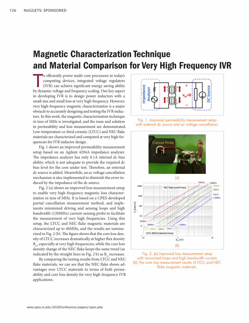
126
www.cpes.vt.edu/2016Conference/papers/spon.php
NUGGETS: SPONSORED
To efficiently power multi-core processors in today’s computing devices, integrated voltage regulators (IVR) can achieve significant energy saving ability
by dynamic voltage and frequency scaling. One key aspect in developing IVR is to design power inductors with a small size and small loss at very high frequency. However, very high-frequency magnetic characterization is a major obstacle to accurately designing and testing the IVR induc-tors. In this work, the magnetic characterization technique in tens of MHz is investigated, and the issue and solution in permeability and loss measurement are demonstrated. Low-temperature co-fired ceramic (LTCC) and NEC flake materials are characterized and compared at very high fre-quencies for IVR inductor design.
Fig. 1 shows an improved permeability measurement setup based on an Agilent 4294A impedance analyzer. The impedance analyzer has only 0.1A internal dc bias ability, which is not adequate to provide the required dc bias level for the core under test. Therefore, an external dc source is added. Meanwhile, an ac voltage cancellation mechanism is also implemented to diminish the error in-duced by the impedance of the dc source.
Fig. 2 (a) shows an improved loss measurement setup to enable very high frequency magnetic loss character-ization in tens of MHz. It is based on a CPES-developed partial cancellation measurement method, and imple-ments minimized driving and sensing loops and high bandwidth (120MHz) current-sensing probe to facilitate the measurement of very high frequencies. Using this setup, the LTCC and NEC flake magnetic materials are characterized up to 40MHz, and the results are summa-rized in Fig. 2 (b). The figure shows that the core loss den-sity of LTCC increases dramatically at higher flux density Bm, especially at very high frequencies, while the core loss density change of the NEC flake keeps the same trend (as indicated by the straight lines in Fig. 2 b) as Bm increases.
By comparing the testing results from LTCC and NEC flake materials, we can see that the NEC flake shows ad-vantages over LTCC materials in terms of both perme-ability and core loss density for very high-frequency IVR applications.
Magnetic Characterization Technique and Material Comparison for Very High Frequency IVR
Fig. 1. Improved permeability measurement setup with external dc source and ac voltage cancellation.
Fig. 2. (a) Improved loss measurement setup with minimized loops and high bandwidth current;
(b) The core loss measurement results of LTCC and NEC flake magnetic materials.
(a)
(b)

127CPES ANNUAL REPORT 2016
www.cpes.vt.edu/2016Conference/papers/spon.php
The stability of integrated power systems has become a concern due to the interaction between controls, leading to potentially unstable operation and requir-
ing the verification of system operation before a design can be implemented. The conservative stability criteria for dc distributed power systems is based on the ratio of the source and load impedances. In order to design a robust power system for which stable operation can be guaranteed, th precise identification of small-signal dq impedances is necessary. The characterization of small-signal dq imped-ances is usually implemented either with voltage or current injections. The injection of single-phase wide-bandwidth signals into three-phase ac power systems significantly re-duces the measurement time required, and uses the a mini-mal number of hardware components.
The interleaved transformerless H-bridge converter (Fig. 1) is optimized to operate as a series voltage injector,
increasing the low-frequency injection range by avoiding transformer saturation problems. Decoupling control is implemented, providing an effective way to balance dc capacitor voltages and regulate the series injection volt-age. The modular and scalable single-phase impedance measurement unit (IMU) is designed and constructed to inject chirp, multi-tone and sinusoidal signals in series with the three-phase ac power systems. The measure-ment system is designed to inject all three types of signals in the full frequency range, offering a trade-off between measurement time, precision, and the number of iden-tification points. The effectiveness of the proposed iden-tification approach is verified with an online estimation of source and load impedances of an actively controlled, programmable voltage source and a three-phase resistive load, as shown in Fig. 2.
Wide-bandwidth Identification of Small-Signal dq Impedances of AC Power Systems via Single-Phase Series Voltage Injection
Fig. 1. Interleaved transformerless series voltage injection converter.
Fig. 2. Source small-signal dq impedance calculated with FFT algorithm (straight red line) and cross-correlation
method (straight blue line):
(a). Zdd(s) (b). Zdq(s) (c). Zqd(s) (d). Zqq(s).

128
www.cpes.vt.edu/2016Conference/papers/spon.php
NUGGETS: SPONSORED
Today’s on-board battery chargers for hybrid electric vehicles usually consist of two stages; an ac-dc PFC stage, which converts the ac line input to a 400V
dc-link, and an isolated dc-dc stage, which regulates the 400V dc-link to 250V–450V battery voltage. For the sec-ond stage, using the CLLC resonant converter has become very popular due to its inherent soft-switch-ing mechanism and bi-directional capability. In ad-dition, with the maturity of wide-band-gap devices, there is an opportunity to push the switching fre-quency up to the MHz range, bringing the efficiency and power density of the secondary stage into a new level. However, the wide battery voltage range posts a great challenge to the design of the resonant con-verter. When the gain required by the second stage is not unity, the switching frequency will deviate from the resonant frequency, resulting in low efficiency.
In order to make the CLLC resonant converter work at its optimal point, two candidate structures are evaluated and compared in terms of efficiency: a con-ventional fixed 400V dc-link voltage structure using GaN devices, and a variable 500V–840V dc-link voltage struc-ture with mixed wide-band-gap devices, as shown in Fig. 1. It is shown that the latter candidate has the smallest gain range, as shown in Fig. 2, resulting in a smaller fre-quency range and lower loss. In order to handle the high dc-link voltage, 1.2kV SiC devices are used in the PFC stage and the primary side of the dc-dc stage, while 650V GaN devices are used as secondary-side synchronous rectifier. In addition, a two-stage combined control strat-egy is proposed, as shown in Fig. 1. The blue line shows the PFC stage control, which is responsible for keeping the average dc-link voltage tracking the battery voltage. The green line represents the control used to control the switching frequency of the CLLC resonant converter. The red and yellow lines represent a non-linear function to determine the battery charging stage. By using this pro-posed structure, the switching frequency of the resonant converter is always kept around the resonant frequency, which gives the best efficiency.
A 6.6kW 500kHz prototype is built to verify the pro-posed two-stage system structure and control strategy.
The efficiency results are shown in Fig. 3, as is the hard-ware, which uses a PCB winding transformer with leakage integration. Efficiency of 97.6% can be achieved over the entire battery voltage range.
A Novel High-Efficiency System Architecture for a Bi-directional On-Board Battery Charger
Fig. 1. Proposed system structure and control.
Fig. 2. Gain range and frequency range comparison.
Fig. 3. Efficiency comparison.
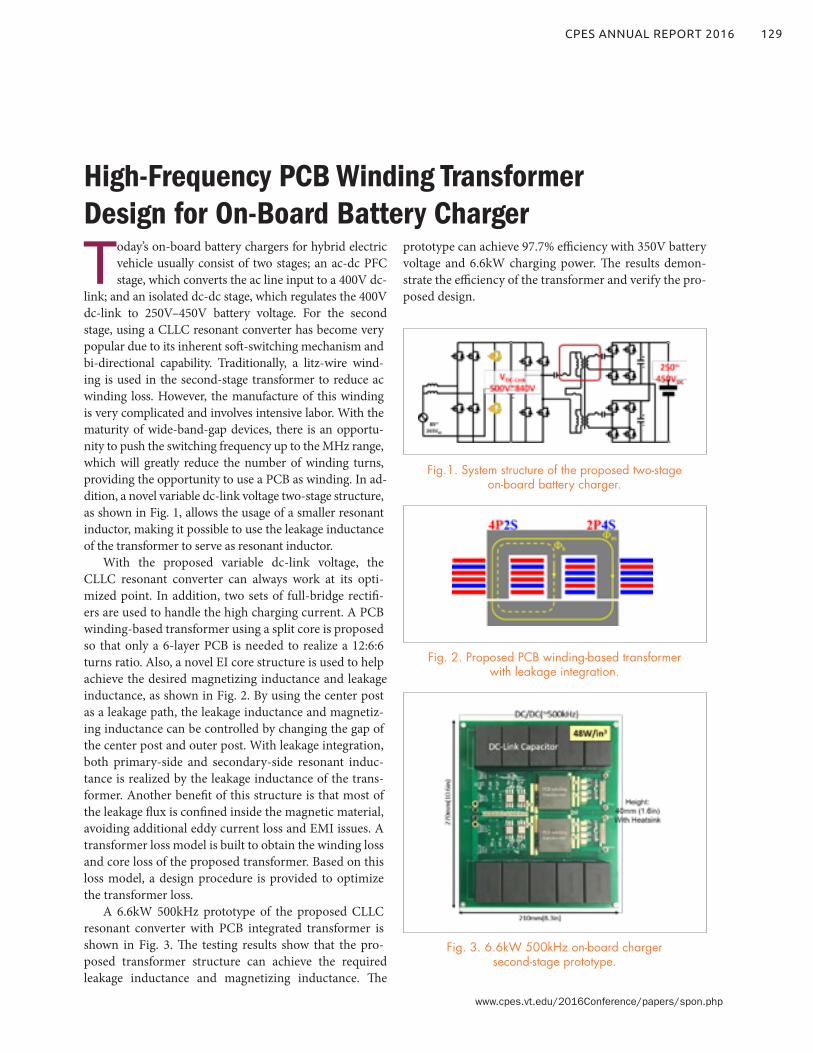
129CPES ANNUAL REPORT 2016
www.cpes.vt.edu/2016Conference/papers/spon.php
Today’s on-board battery chargers for hybrid electric vehicle usually consist of two stages; an ac-dc PFC stage, which converts the ac line input to a 400V dc-
link; and an isolated dc-dc stage, which regulates the 400V dc-link to 250V–450V battery voltage. For the second stage, using a CLLC resonant converter has become very popular due to its inherent soft-switching mechanism and bi-directional capability. Traditionally, a litz-wire wind-ing is used in the second-stage transformer to reduce ac winding loss. However, the manufacture of this winding is very complicated and involves intensive labor. With the maturity of wide-band-gap devices, there is an opportu-nity to push the switching frequency up to the MHz range, which will greatly reduce the number of winding turns, providing the opportunity to use a PCB as winding. In ad-dition, a novel variable dc-link voltage two-stage structure, as shown in Fig. 1, allows the usage of a smaller resonant inductor, making it possible to use the leakage inductance of the transformer to serve as resonant inductor.
With the proposed variable dc-link voltage, the CLLC resonant converter can always work at its opti-mized point. In addition, two sets of full-bridge rectifi-ers are used to handle the high charging current. A PCB winding-based transformer using a split core is proposed so that only a 6-layer PCB is needed to realize a 12:6:6 turns ratio. Also, a novel EI core structure is used to help achieve the desired magnetizing inductance and leakage inductance, as shown in Fig. 2. By using the center post as a leakage path, the leakage inductance and magnetiz-ing inductance can be controlled by changing the gap of the center post and outer post. With leakage integration, both primary-side and secondary-side resonant induc-tance is realized by the leakage inductance of the trans-former. Another benefit of this structure is that most of the leakage flux is confined inside the magnetic material, avoiding additional eddy current loss and EMI issues. A transformer loss model is built to obtain the winding loss and core loss of the proposed transformer. Based on this loss model, a design procedure is provided to optimize the transformer loss.
A 6.6kW 500kHz prototype of the proposed CLLC resonant converter with PCB integrated transformer is shown in Fig. 3. The testing results show that the pro-posed transformer structure can achieve the required leakage inductance and magnetizing inductance. The
prototype can achieve 97.7% efficiency with 350V battery voltage and 6.6kW charging power. The results demon-strate the efficiency of the transformer and verify the pro-posed design.
High-Frequency PCB Winding Transformer Design for On-Board Battery Charger
Fig. 3. 6.6kW 500kHz on-board charger second-stage prototype.
Fig.1. System structure of the proposed two-stage on-board battery charger.
Fig. 2. Proposed PCB winding-based transformer with leakage integration.
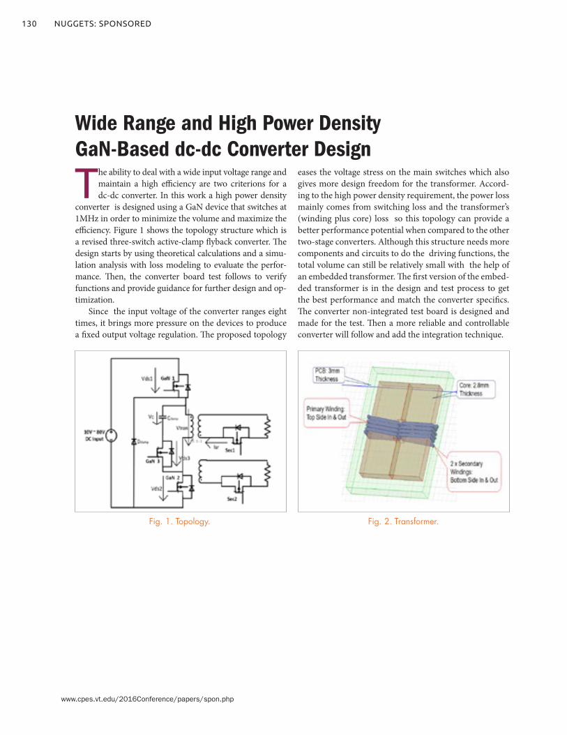
130
www.cpes.vt.edu/2016Conference/papers/spon.php
NUGGETS: SPONSORED
The ability to deal with a wide input voltage range and maintain a high efficiency are two criterions for a dc-dc converter. In this work a high power density
converter is designed using a GaN device that switches at 1MHz in order to minimize the volume and maximize the efficiency. Figure 1 shows the topology structure which is a revised three-switch active-clamp flyback converter. The design starts by using theoretical calculations and a simu-lation analysis with loss modeling to evaluate the perfor-mance. Then, the converter board test follows to verify functions and provide guidance for further design and op-timization.
Since the input voltage of the converter ranges eight times, it brings more pressure on the devices to produce a fixed output voltage regulation. The proposed topology
eases the voltage stress on the main switches which also gives more design freedom for the transformer. Accord-ing to the high power density requirement, the power loss mainly comes from switching loss and the transformer’s (winding plus core) loss so this topology can provide a better performance potential when compared to the other two-stage converters. Although this structure needs more components and circuits to do the driving functions, the total volume can still be relatively small with the help of an embedded transformer. The first version of the embed-ded transformer is in the design and test process to get the best performance and match the converter specifics. The converter non-integrated test board is designed and made for the test. Then a more reliable and controllable converter will follow and add the integration technique.
Wide Range and High Power Density GaN-Based dc-dc Converter Design
Fig. 1. Topology. Fig. 2. Transformer.

131CPES ANNUAL REPORT 2016
www.cpes.vt.edu/2016Conference/papers/spon.php
Plug-in electric vehicles (PEVs), which include plug-in hybrid electric vehicles (PHEVs) and battery electric vehicles (BEVs), are becoming more and
more popular due to more efficient energy utilization and less combustion emission. One crucial challenge of PEV’s commercialization is the demand for a lightweight, com-pact, and efficient on-board charger (OBC) system. The state-of-the-art level-2 OBC products are predominantly Si-based design, which has a switching frequency of less than 100kHz, a 3–12W/in3 power density, and at most a 92–94% efficiency. In addition, the feature of bidirectional power flow of the OBC system is strongly desired by con-sumers according to market research conducted by auto-mobile companies. However, Si-based OBC products can-not provide this function without significant sacrifice to power density and/or efficiency.
The emerging wide-band-gap (WBG) power semi-conductor devices provide the enabling technology to dramatically increase the efficiency and power density of switch-mode power supplies with potential lower cost and better manufacturability. Therefore, by using WBG devices to design the 6.6kW OBC system, the target is to increase the switching frequency to higher than 300kHz with doubled or tripled power density, at least 95% effi-ciency, and bi-directional power flow capability.
In this research, four different system architectures are, first evaluated and compared. The best candidate is the proposed novel variable dc-link voltage system ar-chitecture. Then, the focus of this paper will turn to the design of the ac-dc stage so that detailed design consider-ations are elaborated, including the evaluation of 1.2kV SiC MOSFETs for device selection; a programmed extra off-time function to realize a whole line cycle zero-volt-age-switching (ZVS) and eliminate dominant turn-on loss; and a proposed universal control strategy for both rectifier mode and inverter mode operation. Finally, a prototype is demonstrated with 98.5% efficiency and 47W/in3 power density of the ac-dc stage and 96% effi-ciency and 24W/in3 power density of the total system.
High-Frequency CRM AC-DC Converter for WBG-Based 6.6kW On-Board Charger
Fig. 1. Prototype of 6.6kW on-board charger.
Fig. 2. Tested efficiency.
Fig. 3. Proposed inverter control.
132
www.cpes.vt.edu/2016Conference/papers/spon.php
NUGGETS: SPONSORED
To obtain the high power capability required by in-dustries such as welding machines, traction drives and automotive electronics, several MOSFETs can
be paralleled to increase the current rating. However, de-vice mismatches introduce current sharing among them. Current de-rating is needed to maintain a reliable opera-tion, which leads to increased number of dice, cost and volume. Among all the device parameters, on-state re-sistance (Rds(on)) and threshold voltage (Vth) are the most critical ones, which causes steady-state current sharing and dynamic current sharing, respectively. Since Rds(on) has a positive temperature coefficient, it will not lead to ther-mal run-away. Nevertheless, Vth has a negative temperature coefficient and will worsen the dynamic sharing when an imbalance exists.
Parasitic inductances are introduced by package or layout that electrically connects bare dies. Much research focuses on dynamic sharing caused by asymmetric lay-out, which can be easily removed by a careful layout de-sign. However, the existing methods to mitigate dynamic sharing origins from device mismatch are usually com-plex and expensive, which normally require separate gate drivers, complex current sensing and an active control circuit. This paper introduces a simple and passive meth-od to reduce transient sharing caused by Vth mismatch.
The equivalent circuit model considering all the para-sitic inductances is shown in Fig. 1. The objective of this paper is to mitigate the imbalance caused by device mis-match. Symmetrical layout is employed in order to avoid the imbalance origins from an external package. Their influences on parallel dynamic performance are compre-hensively investigated with regard to switching loss, volt-age stress, and switching loss imbalance.
Influence of Lks and Ls on switching loss imbalance is shown in Fig. 2. According to the results, Lks and Ls can greatly reduce dynamic sharing between M1 and M2. Even though Ls will increase device voltage stress together with small power-loop inductance Lp, the voltage stress, as
long as it is not super large and stays within the nH level, can be controlled within an acceptable range. Further-more, switching loss is not sacrificed.
Dynamic Sharing Between Paralleled SiC MOSFETs Caused by Threshold Voltage Mismatch
Fig. 1. Schematic of double-pulse tester with low-side switch composed of two SiC MOSFETs in parallel.
Fig. 2. Influence of Lks and Ls on switching loss imbalance with all the other inductances equal to 0 nH,
Vth1 = 2.48V and Vth2 = 3.08V.
133CPES ANNUAL REPORT 2016
www.cpes.vt.edu/2016Conference/papers/spon.php
Spurious turn-on occurs in a discrete phase leg com-prising two MOSFETs when both dice are turned on simultaneously and generate an observable current
spike. Simulation of a module of paralleled dice reveals internal spurious turn-on even in the absence of current spike at the terminals. Power modules with well-behaved terminal waveforms could still have their dice suffering from spurious turn-on (cross-turn-on and self-turn-on). Compared to self-turn-on, which is mainly induced by the common-source inductance, cross-turn-on deserves more attention because of its common appearance and severity for the modules with Kelvin-source connection, which has been a standard configuration for SiC module manufac-turer.
The SPICE model of one commercial module is devel-oped and verified with a higher accuracy than the com-mercial SPICE model. The total switching energy and sus-ceptibility to cross-turn-on for two modules tailored from the commercial layouts are investigated by studying the simulated channel current of each MOSFET die and ter-minal current of the module in the presence of packages’
parasitic impedances. The total switching energy, which is the sum of the switching energy and extra energy induced by cross-turn-on of the asymmetrical module, can be as high as 322% of the conventionally defined switching energy, which clarifies severity of cross-turn-on for the high-voltage and fasting-switching application of paral-leled SiC MOSFETs.
A symmetrical layout decreases extra energy induced by cross-turn-on while maintaining a similar total switch-ing energy under a low input voltage (< 400V) applica-tion and a lower total switching energy under a high input voltage (> 400V) application as compared to an asymmet-rical layout. The symmetrical layout significantly reduces the peak cross-turn-on current stress on die, which is only 10.6% of the current for the asymmetrical case. Besides the layout symmetry, a paralleling SiC Schottky diode also reduces cross-turn-on current to 21.3% of the origi-nal value. Decreasing the gate and Kelvin-Source induc-tance doesn’t greatly mitigate the problem and increasing external gate resistance suppresses cross-turn-on at the expense of a higher total switching energy.
Spurious Turn-On inside a Power Module of Paralleled SiC MOSFETs
Fig. 1. Comparison among experimental results, simulated results by commercial SPICE model,
and simulated results by developed SPICE model.
Fig. 2. Ratio between (Ecross + Eswitch) and Eswitch of asymmetrical module and symmetrical module when input
voltage (Vin),low-side gate resistance (Rglow), and (c) switching current (Iswitch) vary.
134
www.cpes.vt.edu/2016Conference/papers/spon.php
NUGGETS: SPONSORED
Designing and building a medium voltage (MV) IMU poses several challenges, but with respect to the MV environment, the issues of operating in
an MV environment with multiple switching converters and sensitivity to possibly high levels of common-mode currents have been identified as significant. While sev-eral challenges have been addressed during earlier project phases, this MV laboratory testing explores the practical applicability of impedance measurement approaches at meaningfully high voltage and power levels. The labora-tory tests described in this paper follow and complement modeling, simulation and controller Hardware-in-the-Loop efforts.
Three major test setups are of primary interest: the basic Power Electronics Building Blocks (PEBB)-based modules of the IMU are tested for voltage and current capabilities, ac impedance measurement in a three-wire ac system, and dc impedance measurement.
The PEBB tests were successfully executed, and heat runs were performed to confirm the design. Examples of dc and ac voltages conditions are shown in Fig. 1. The PEBBs were operated with up to 4kV on the dc side and a modulation index commanded to generate ac voltages.
Fig. 2(a) shows the load impedance as measured by the IMU in the ac setup while operating at 480V ac. The result reflects to a large part the connected resistive load with some inductive components. The IMU operation has to take place in an environment that shows switch-ing level distortions at various levels: Fig. 2(b) shows the ac voltage and current as measured with a 10kHz low-pass filter (normalized quantities). The voltage and cur-rent have been recorded while perturbing the ac system at 680Hz, and the surrounding system shows significant levels of common-mode currents and distortions in volt-ages and current.
The next tests will evaluate the IMU capabilities when connecting one of the MMCs as the load rather than the passive load bank. The MMC connected to the IMU acts as the ac-dc converter, and another MMC will be used to set the dc system loading conditions.
Testing of a Novel Medium-Voltage Impedance Measurement Unit
Fig. 1. (a) dc voltage and (b) ac voltage example during PEBB power stage testing.
Fig. 2. (a) Example ac impedance measurement result and (b) Example ac voltage and current waveforms while IMU
injects perturbation.
(a)
(b)

135CPES ANNUAL REPORT 2016
www.cpes.vt.edu/2016Conference/papers/spon.php
With the higher electromagnetic interference (EMI) noise generated by devices with fast switching speeds, it is crucial to learn about
EMI noise generation and propagation in the systems and design effective EMI filters. An EMI behavioral model has been verified as an effective tool to predict common-mode (CM) or differential-mode (DM) EMI noise and aid in EMI filter design. There also exists, in addition to the CM and DM noise, a third mode of noise in the system—mixed-mode (MM) noise —which cannot be captured by existing EMI models. The model presented here is ex-tracted to predict DM noise with mixed-CM noise based on a three-phase SiC inverter with its parasitic capacitive impedance to the ground (CPG, CNG, and COG), as illustrated in Fig. 1.
The experimental measurements with different CM and DM chokes show that on the input side of this set-up the DM input noise is coupled with CM noise, and is dependent on the CM noise propagation path in the sys-tem. The DM input model should consider the CM com-ponents: the CM noise propagation path and CM noise sources. Then the mixed-mode unterminated behavioral model (MUBM) is proposed, shown by the dashed line in Fig. 2, which contains the entire propagation path at the input, including the parasitics like CPG and CNG, that are il-lustrated in Fig. 1. From the model, it can be derived that the DM noise is independent of ISCM and ZL if and only if ZPG and ZNG are equal. If ZPG and ZNG are equal, or CPG and CNG are symmetric, the DM noise is generated only by and propagates within the DM loop. Otherwise, ZL and ISCM have an effect on the DM noise.
In order to extract the five model parameters, there are two experiments performed: one to determine
the noise sources, the other to determine ZPG and ZNG. ZL can be measured with the impedance analyzer. With the model, the DM noise can be calculated or predicted. Fig. 3 provides a comparison between the model predic-tions and the experimental measurements of the DM noise, where there is a good match between the predic-tion and the measurements above 30MHz. Furthermore, Fig. 3 also shows that with a different EMI filter, or with a different CM or DM propagation impedance, the model can capture the change and predict the DM noise accu-rately.
The imbalance of ZPG and ZNG comes from the asym-metric parasitic capacitors in the phase-leg model. The proposed model MUBM can be applied to other symmet-ric topologies, such as a full-bridge converter.
Differential-mode EMI emission prediction of SiC-based power converters using a mixed-mode unterminated behavioral model
Fig. 1. Three-phase power inverter diagram and the experimental setup.
Fig. 2. Proposed mixed-mode terminated behavioral model.
Fig. 3. The comparison of the measured (light) and predicted (black) DM spectrum (a):
Without CM or DM choke; (b): With CM choke.
(b)
(a)

136
www.cpes.vt.edu/2016Conference/papers/spon.php
NUGGETS: SPONSORED
The SiC MOSFET, when used as a wide-bandgap de-vice, has superior performance for its high break-down electric field, low on-state resistance, fast
switching speed and high working temperature. The high switching speed enables a high switching frequency, which improves the power density of high-power converters. The cost of the SiC MOSFET is also gradually decreasing due to its growing of usage in industry applications. Therefore, the SiC MOSFET is of great potential in medium-voltage (MV) high power applications as a substitute for Si IG-BTs. A well-performing gate driver with sufficient protec-tions is critical to ensure excellent performance of a SiC MOSFET module. The driver must be capable of features such as low propagation delay, high driving current, good dv/dt immunity, and effective protections that includes
correct detection and fast responses.This paper compares different configurations and pro-
poses a best power architecture for dv/dt immunity, as shown in Fig. 1. On the basis of these findings, the driv-er IC is selected from a number of candidates. Next the external current booster, soft turn-off and active Miller clamp circuitry are designed for the selected driver IC. A conventional desaturation short circuit protection circuit is kept in the circuit design, but an additional short-circuit protection circuit based on the Rogowski current sensor on the PCB board is added for effective protection. The test results obtained from the experimental setup (shown in Fig. 2) show that all the designed circuitry has good performance for device driving and protection.
Gate Driver Design for 1.7kV SiC MOSFET Module with Rogowski Current Sensor for Short-circuit Protection
Fig. 1. Design architecture.
Fig. 2. Experimental setup.

137CPES ANNUAL REPORT 2016
www.cpes.vt.edu/2016Conference/papers/spon.php
In modern aircraft power systems, transformer rectifier units are widely adopted to perform ac-dc power con-version while also providing galvanic isolation. Recent
research shows that active rectifiers are promising replace-ments for transformer rectifier units concerning efficiency and weight. Furthermore, active rectifiers can perform on-line current shaping and output voltage regulation, which is out of reach for transformer rectifier units. To exploit the benefits of active rectifiers, converter design and optimiza-tion should be carefully made under the requirements of aircraft applications: electromagnetic interference (EMI) standards, power quality standards, etc. Moreover, certain applications may have strict limits on converter specifica-tions: weight, size, converter loss, etc. This paper focuses on the design and optimization of a free convection cooled isolated three-phase active ac-dc converter that delivers maximum power within the given dimensions (8 inches × 7.5 inches × 1 inch), loss (35W) limits and operation (EMI, power quality) requirements.
A two-stage structure (shown in Fig. 1), where an active front-end (AFE) converter is joined with an iso-lated dc-dc converter, was employed in this design. The AFE stage converts a three-phase variable frequency
(360Hz–800Hz) ac voltage (115 Vrms) into a regulated dc voltage while performing a power factor correction for the inputs. An isolated dc-dc stage converts internal dc bus voltage into output dc bus voltage (28V) while pro-viding galvanic isolation. Input EMI filters were added to meet EMI standard. A complete design and optimization method was developed in search of the relationship be-tween the converter rated power, full load loss and con-verter size of this multi-converter system. A 1.2kW con-verter prototype (shown in Fig. 2) was constructed based on the design and optimization results. The 1.2kW free convection cooled prototype exhibits a 97.1% full load ef-ficiency and a 22W/inch3 power density. The compliance of EMI standards and power quality standards was veri-fied experimentally.
Design and Optimization of a High Performance Isolated Three Phase AC-DC Converter
Fig. 2. Converter prototype. Fig. 3. Experimental wave.
Fig. 1. System structure.

138
www.cpes.vt.edu/2016Conference/papers/spon.php
NUGGETS: SPONSORED
Small-signal stability is of great concern for electrical power systems with a large number of regulated power converters. In the case of dc systems, stability can be
predicted by examining the locus described by the ratio of the source and load impedances in the complex plane per the Nyquist stability criterion. In the case of three-phase ac systems, the impedance-based stability can be formulated using the synchronous d-q frame source and load imped-ances. Recently, the use of the generalized Nyquist stability criterion (GNC) was proposed to predict the stability at the ac interfaces in the d-q frame. This paper studies the small-signal stability of an ac system comprised of a voltage-source inverter (VSI) feeding a boost rectifier or voltage-source converter (VSC), in what is regarded to be a very generic system configuration.
The paper discusses how stable and unstable cases are created in the experimental system, shown in Fig. 1, based on the derived d-q frame average model of both the VSI and VSC. The constant power loads and instability condi-tions are also considered, but solely through the d-d chan-
nel. The d-q frame impedance measurement techniques and algorithm are then discussed. The experimental re-sults, including time-domain waveforms and measured d-q frame impedances, like Fig. 2, validate all stability condi-tions. Because of its accuracy, using this approach to predict stability in both the frequency domain and time domain has the potential to enable the use of impedance specifica-tion as a design tool for future ac systems.
Small-Signal Stability Analysis of Three-Phase Ac Systems in the Presence of Constant Power Loads Based on Measured d-q Frame Impedances
Fig. 2. Measurement results of one case: (a) Time-domain results; (b) d-q impedance.
(a) (b)
Fig. 1. Experimental system setup and control scheme.

139CPES ANNUAL REPORT 2016
www.cpes.vt.edu/2016Conference/papers/spon.php
Bonding chips by sintering silver particles (on the mi-cron scale or nanometer scale) is widely believed to be suitable for replacing soldering in the manufac-
ture of high-performance power semiconductor devices and modules because sintered silver joints are better for heat dissipation and more reliable in temperature-cycling and power-cycling tests than soldered joints. Common raw materials used for the silver sintering process are in the form of paste consisting of silver particles mixed in an or-ganic system of binders, surfactants, and solvents. In our recent studies, we developed a mathematical model based on the diffusion of solvent molecules and viscous-flow me-chanics of a silver paste to show that drying of the paste in the bonding process is a critical step in determining the microstructural and mechanical quality of the bond-line. Our modeling results showed that stresses and strains generated in the shrinking silver paste were responsible for observed delamination and cracking in the sintered bond-line. In this study, we extended the modeling analy-sis to investigate the effects of heating rate on the bond-line quality. A numerical simulation algorithm of the model was developed to determine the time-dependent physical properties of the silver paste as it was being dried at differ-ent heating rates. The simulation results showed a strong dependence of the relative density of the sintered bond-line on heating rate. By lowering the heating rate, the relative density of the sintered silver could be increased. A higher sintered density would mean stronger bonding strength, and this was verified by our experimental data. The find-ings of this study can be used to optimize the manufactur-ing process that uses sintering of silver paste for bonding power semiconductor chips.
The effect of the heating rates of 1° C/min, 3° C/min, and 7.5° C/min on the bonding strength of sintered nanosilver joint was studied. A diffusion-viscous model was developed to analyze the stress-strain state inside the silver paste bond-line, and numerical simulations were carried out to determine the internal stresses and bond-
line shrinkage during the drying process. We found that tensile stresses generated in the paste bond-line increase with the increasing heating rate and decreasing chip size. Storing samples at room temperature for an extended pe-riod of time helps to lower the internal stresses. The inter-nal stresses reduce bond-line shrinkage, leading to lower relative green density of a dried bond-line, which in turn lowers the sintered density and the bonding strength.
Effect of Heating Rate on Bonding Strength of Pressure-free Sintered Nanosilver Joint
Fig. 1. Parameter combinations of drying process and correlated bond-shearing strength of attached samples.
Fig. 2. Simulated bond-line shrinkages after the various drying profiles.

140
www.cpes.vt.edu/2016Conference/papers/spon.php
NUGGETS: SPONSORED
A phase-leg or half-bridge can serve as the build-ing block for many power conversion topolo-gies. When the positive and negative nodes of
the phase-leg are connected to a voltage source, the peak voltage of each switch is clamped to the source voltage. This configuration of voltage-fed phase-legs is preferable to GaN transistors which have a lack of avalanche capabil-ity. Both the power loop and gate loop are self-contained inside the module, enabling minimized inductances, reli-able switching, and low loss. But this building block, as Fig. 1 shows, is still incomplete without two peripheral circuits: floating drives to interface with the PWM gener-ating board, and sensing circuits of the phase-leg voltages and currents for control and protection purposes. These two parts of the circuitry have to survive the highly noisy environment of GaN switching.
The key to designing the driving channel with high common-mode transient immunity (CMTI) is to provide a high impedance between the high-voltage/high-power side of the GaN MCM to the low-power side that comes from the control circuit. The power supply and the gate drive are selected with very small intercapacitance, whose effect is illustrated in Fig. 2. A Y-capacitor filter is added to avoid noise flowing into DSP control board. Addition-ally, the PCB layout is considered. For example, to mini-mize the parasitic capacitance generated by the layout,
the copper layers of the primary side and secondary side should be without overlap.
In order to achieve reliable sensing in the very noisy GaN switching environment, the dc voltage sensor re-quires a low-pass filter stage and needs to be placed out-side the full-bridge board; the ac current sensor should not be separated from the switching node by a high-im-pedance component, such as an inductor, and therefore will also be outside the full-bridge board, while the dc current sensor can be left on the full-bridge board. Invert-er tests are performed with 300V, 6A and 500kHz, with and without the techniques implemented; the sensing re-sults are shown in Fig. 3. These clean sensing results are critical to the closed-loop control of the system.
Driving and sensing design of an enhancement-mode-GaN phase-leg as a building block
Fig. 1. Layout of a full-bridge building block.
Fig. 2. Waveforms (a) without and (b) with SIB610EC-B-IS digital isolator.
(b)
(a)
Fig. 3. Sensing results (a) without and (b) with the techniques.
(b)
(a)

141CPES ANNUAL REPORT 2016
www.cpes.vt.edu/2016Conference/papers/spon.php
For many years, the coupled inductor has been widely adopted in VR applications because of its benefits such as reducing current ripple or improving tran-
sient performance. Previously, the negative coupled in-ductor was applied to the interleaved MHz totem-pole CRM PFC converter for server power supply. In this paper, the positive coupled inductor concept is applied to the interleaved totem-pole CRM PFC converter for a 6.6kW on board battery charger and the difference be-tween negative coupling and positive coupling will be dis-cussed. The benefits of positive coupling for the battery charger, such as reducing the switching frequency range
and reducing the input DM noise will be presented, thus showing that the positive coupled inductor can improve the performance of the PFC converter. In addition, a bal-ance technique is applied to help minimize the CM noise. Previously, the balance technique was developed for an interleaved boost PFC converter with independent in-ductors. This presentation will introduce how to achieve balance with a coupled inductor. Last but not least, the inductor will be integrated into a PCB winding with little sacrifice on loss. With the inductor integration, the con-verter can avoid labor intensive production and achieve a fully automatic manufacture.
Inductor Coupling and Integration for 6.6kW On Board Battery Charger
Fig. 1. Interleaved Totem-Pole PFC with Positive Coupled Inductor and Balance Technique
Fig. 1. Inductor core structure (principle drawing).
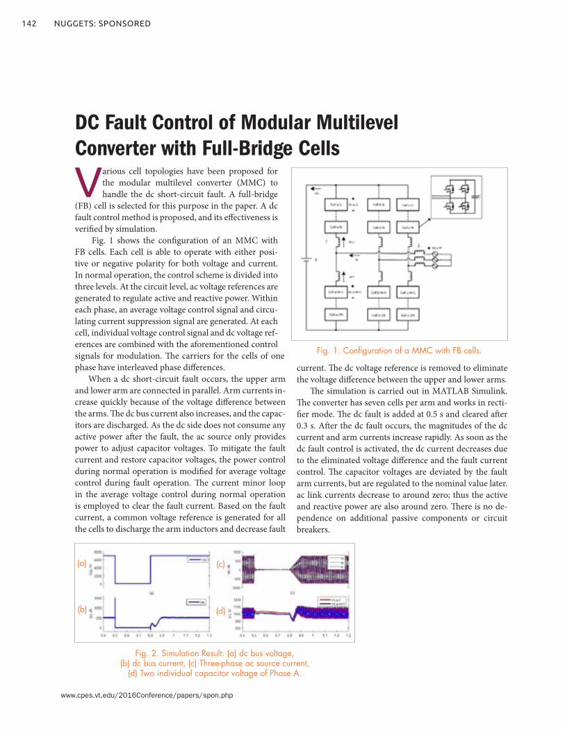
142
www.cpes.vt.edu/2016Conference/papers/spon.php
NUGGETS: SPONSORED
Various cell topologies have been proposed for the modular multilevel converter (MMC) to handle the dc short-circuit fault. A full-bridge
(FB) cell is selected for this purpose in the paper. A dc fault control method is proposed, and its effectiveness is verified by simulation.
Fig. 1 shows the configuration of an MMC with FB cells. Each cell is able to operate with either posi-tive or negative polarity for both voltage and current. In normal operation, the control scheme is divided into three levels. At the circuit level, ac voltage references are generated to regulate active and reactive power. Within each phase, an average voltage control signal and circu-lating current suppression signal are generated. At each cell, individual voltage control signal and dc voltage ref-erences are combined with the aforementioned control signals for modulation. The carriers for the cells of one phase have interleaved phase differences.
When a dc short-circuit fault occurs, the upper arm and lower arm are connected in parallel. Arm currents in-crease quickly because of the voltage difference between the arms. The dc bus current also increases, and the capac-itors are discharged. As the dc side does not consume any active power after the fault, the ac source only provides power to adjust capacitor voltages. To mitigate the fault current and restore capacitor voltages, the power control during normal operation is modified for average voltage control during fault operation. The current minor loop in the average voltage control during normal operation is employed to clear the fault current. Based on the fault current, a common voltage reference is generated for all the cells to discharge the arm inductors and decrease fault
current. The dc voltage reference is removed to eliminate the voltage difference between the upper and lower arms.
The simulation is carried out in MATLAB Simulink. The converter has seven cells per arm and works in recti-fier mode. The dc fault is added at 0.5 s and cleared after 0.3 s. After the dc fault occurs, the magnitudes of the dc current and arm currents increase rapidly. As soon as the dc fault control is activated, the dc current decreases due to the eliminated voltage difference and the fault current control. The capacitor voltages are deviated by the fault arm currents, but are regulated to the nominal value later. ac link currents decrease to around zero; thus the active and reactive power are also around zero. There is no de-pendence on additional passive components or circuit breakers.
DC Fault Control of Modular Multilevel Converter with Full-Bridge Cells
Fig. 2. Simulation Result: (a) dc bus voltage, (b) dc bus current, (c) Three-phase ac source current,
(d) Two individual capacitor voltage of Phase A.
(a)
Fig. 1. Configuration of a MMC with FB cells.
(d)(b)
(c)
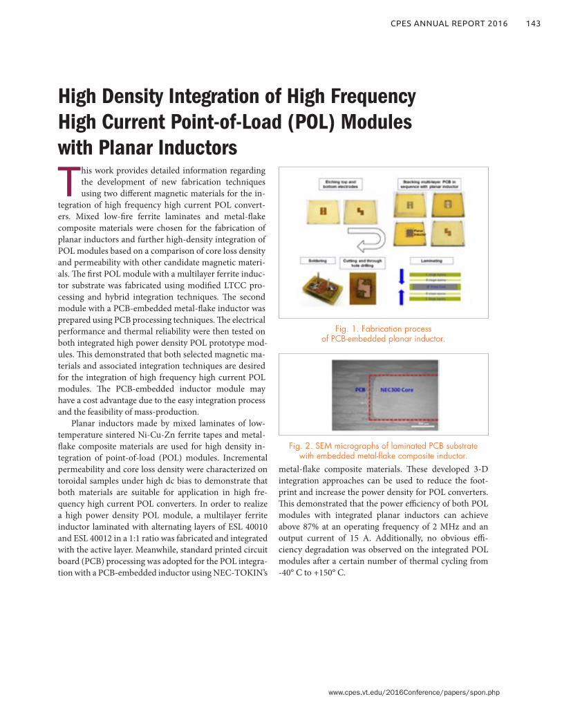
143CPES ANNUAL REPORT 2016
www.cpes.vt.edu/2016Conference/papers/spon.php
This work provides detailed information regarding the development of new fabrication techniques using two different magnetic materials for the in-
tegration of high frequency high current POL convert-ers. Mixed low-fire ferrite laminates and metal-flake composite materials were chosen for the fabrication of planar inductors and further high-density integration of POL modules based on a comparison of core loss density and permeability with other candidate magnetic materi-als. The first POL module with a multilayer ferrite induc-tor substrate was fabricated using modified LTCC pro-cessing and hybrid integration techniques. The second module with a PCB-embedded metal-flake inductor was prepared using PCB processing techniques. The electrical performance and thermal reliability were then tested on both integrated high power density POL prototype mod-ules. This demonstrated that both selected magnetic ma-terials and associated integration techniques are desired for the integration of high frequency high current POL modules. The PCB-embedded inductor module may have a cost advantage due to the easy integration process and the feasibility of mass-production.
Planar inductors made by mixed laminates of low-temperature sintered Ni-Cu-Zn ferrite tapes and metal-flake composite materials are used for high density in-tegration of point-of-load (POL) modules. Incremental permeability and core loss density were characterized on toroidal samples under high dc bias to demonstrate that both materials are suitable for application in high fre-quency high current POL converters. In order to realize a high power density POL module, a multilayer ferrite inductor laminated with alternating layers of ESL 40010 and ESL 40012 in a 1:1 ratio was fabricated and integrated with the active layer. Meanwhile, standard printed circuit board (PCB) processing was adopted for the POL integra-tion with a PCB-embedded inductor using NEC-TOKIN’s
metal-flake composite materials. These developed 3-D integration approaches can be used to reduce the foot-print and increase the power density for POL converters. This demonstrated that the power efficiency of both POL modules with integrated planar inductors can achieve above 87% at an operating frequency of 2 MHz and an output current of 15 A. Additionally, no obvious effi-ciency degradation was observed on the integrated POL modules after a certain number of thermal cycling from -40° C to +150° C.
High Density Integration of High Frequency High Current Point-of-Load (POL) Modules with Planar Inductors
Fig. 1. Fabrication process of PCB-embedded planar inductor.
Fig. 2. SEM micrographs of laminated PCB substrate with embedded metal-flake composite inductor.

www.cpes.vt.edu
Center for Power Electronics Systems – Virginia Tech
1185 Perry Street655 Whittemore HallBlacksburg, VA 24061