Embed Size (px)
Citation preview

Anne-Marie MagnanImperial College London
A MAPS-based digital Electromagnetic Calorimeter for
the ILC
on behalf of the MAPS group:Y. Mikami, N.K. Watson, O. Miller, V. Rajovic, J.A. Wilson
(University of Birmingham)J.A. Ballin, P.D.Dauncey, A.-M. Magnan, M. Noy
(Imperial College London)J.P. Crooks, M. Stanitzki, K.D. Stefanov, R. Turchetta, M. Tyndel, E.G. Villani
(Rutherford Appleton Laboratory)
Saturday, June 2nd, 2007
LCWS 2007 - Hamburg - A.-M.Magnan (IC London) 2
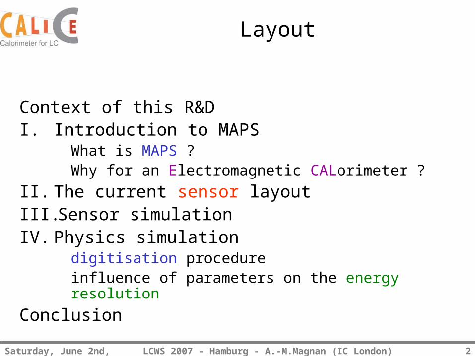
Layout
Context of this R&DI. Introduction to MAPS
What is MAPS ?Why for an Electromagnetic CALorimeter ?
II. The current sensor layoutIII. Sensor simulationIV. Physics simulation
digitisation procedureinfluence of parameters on the energy resolution
Conclusion

Saturday, June 2nd, 2007
LCWS 2007 - Hamburg - A.-M.Magnan (IC London) 3
Context of this R&D
• Alternative to CALICE Si/W analogue ECAL
• No specific detector concept• “Swap-in” solution leaving
mechanical design unchanged
Tungsten1.4 mm
PCB~0.8 mm
Embedded VFE ASIC
Silicon sensor0.3mm
Diode pad calorimeter MAPS calorimeter

Saturday, June 2nd, 2007
LCWS 2007 - Hamburg - A.-M.Magnan (IC London) 4
Introduction to MAPS
• MAPS ? Monolithic Active Pixel Sensor CMOS technology, in-pixel logic: pixel=sensor+readout
electronics 50x50 μm² : reduces probability of multiple hit per pixel Collection of charge mainly by diffusion
• Why for a calorimeter ? high granularity :
better position resolution potentially better PFA performances, or detector more compact reduced cost 1012 pixels : digital readout, DAQ rate dominated by noise Area needed for logic and RAM : ~10% dead area
Cost saving : CMOS vs high resistivity Si wafersPower dissipation : more uniform
challenge to match analog ECAL 1 μW/mm²

Saturday, June 2nd, 2007
LCWS 2007 - Hamburg - A.-M.Magnan (IC London) 5
Sensor layout : v1.0 submitted !
analog circuitry.
comparator+readout logic
4 diodes Ø 1.8 um
Design submitted April 23rd, with several architectures.One example:

Saturday, June 2nd, 2007
LCWS 2007 - Hamburg - A.-M.Magnan (IC London) 6
What’s eating charges : the N-well and P-well distribution in the pixels
pink = nwell (eating charge)
blue = deep p-well added to block the charge absorptionINMAPS process
• Electronics N-well absorbs a lot of charge : possibility to isolate them ?• INMAPS process : deep P-well implant 1 μm thick everywhere under the electronics N-well.

Saturday, June 2nd, 2007
LCWS 2007 - Hamburg - A.-M.Magnan (IC London) 7
• Diode size has been optimised in term of signal over noise ratio, charge collected in the cell in the worse scenario (hit at the corner), and collection time.
• Diodes place is restricted by the pixel designs, e.g. to minimise capacitance effects
The sensor simulation setup
Using Centaurus TCAD for sensor simulation +
CADENCE GDS file for pixel description
Signal over noiseCollected charge
0.9 μm1.8 μm3.6 μm
Saturday, June 2nd, 2007
LCWS 2007 - Hamburg - A.-M.Magnan (IC London) 8
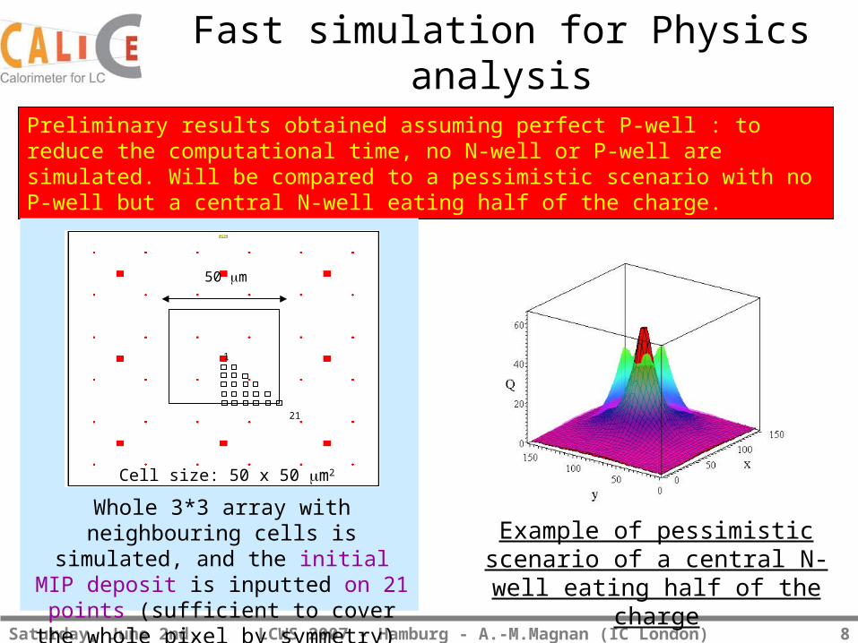
Fast simulation for Physics analysis
Preliminary results obtained assuming perfect P-well : to reduce the computational time, no N-well or P-well are simulated. Will be compared to a pessimistic scenario with no P-well but a central N-well eating half of the charge.
Whole 3*3 array with neighbouring cells is simulated,
and the initial MIP deposit is inputted on 21 points (sufficient to
cover the whole pixel by symmetry)
1
21
50 m
Cell size: 50 x 50 m2
Example of pessimistic scenario of a central N-well
eating half of the charge
Saturday, June 2nd, 2007
LCWS 2007 - Hamburg - A.-M.Magnan (IC London) 9
Physics simulation
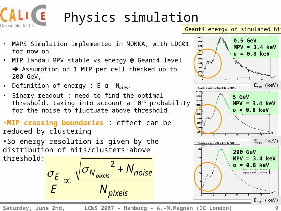
• MAPS Simulation implemented in MOKKA, with LDC01 for now on.
• MIP landau MPV stable vs energy @ Geant4 level Assumption of 1 MIP per cell checked up to 200 GeV,
• Definition of energy : E α NMIPS.
• Binary readout : need to find the optimal threshold, taking into account a 10-6 probability for the noise to fluctuate above threshold.
0.5 GeVMPV = 3.4 keVσ = 0.8 keV
5 GeVMPV = 3.4 keVσ = 0.8 keV
200 GeVMPV = 3.4 keVσ = 0.8 keV
Geant4 energy of simulated hits
Ehit (keV)
Ehit (keV)
Ehit (keV)pixels
noiseNE
N
N
Epixels
2
•MIP crossing boundaries : effect can be reduced by clustering•So energy resolution is given by the distribution of hits/clusters above threshold:

Saturday, June 2nd, 2007
LCWS 2007 - Hamburg - A.-M.Magnan (IC London) 10
Digitisation procedure
Geant4 Einit
in 5x5 μm² cells
Sum energy in 50x50 μm² cells
Esum
Apply charge spreadEafter charge spread
Add noise to signal hitswith σ = 100 eV
(1 e- ~ 3 eV 30 e- noise)
+ noise only hits : proba 10-6 ~ 106 hits in the whole detector
BUT in a 1.5*1.5 cm² tower : ~3 hits.
%Einit
%Einit
%Einit %Einit
%Einit
%Einit %Einit
%Einit
Eini
tRegister the position and the
number of hits above threshold
Importance of the charge spread :
initneighbours EE %)80%50(~

Saturday, June 2nd, 2007
LCWS 2007 - Hamburg - A.-M.Magnan (IC London) 11
Simple clustering
• Loop over hits classified by number of neighbours :• if < 8 : count 1 (or 2 for last 10 layers) and discard neighbours,• if 8 and one of the neighbours has also 8 : count 2 (or 4) and
discard neighbours.• Not very optimised : lots of room for improvement !
600 eV thresh
A particular event, a particular layer
MeV

Saturday, June 2nd, 2007
LCWS 2007 - Hamburg - A.-M.Magnan (IC London) 12
•Neighbouring hit:•hit ? Neighbour’s contribution•no hit ? Creation of hit from charge spread only
•All contributions added per pixel•+ noise σ = 100 eV
How is the energy affected by each digitisation step ?
• E initial : geant4 deposit
•What remains in the cell after charge spread assuming perfect P-well
•+ noise σ = 100 eV, minus dead areas : 5 pixels every 42 pixels in one direction

Saturday, June 2nd, 2007
LCWS 2007 - Hamburg - A.-M.Magnan (IC London) 13
MPV-1σ = 2.5 keV
16% effectDIGITIZED: charge spread with perfect P-well assumed, noise σ=100 eV, 10-5 probability of a pixel to be above threshold dead area removed without or with clustering
Effect of the clustering on the energy resolution
IDEAL : Geant4 energy, no charge spread, no noise, dead area removed (5 pixels every 42 pixels in one direction) without or with clustering
Saturday, June 2nd, 2007
LCWS 2007 - Hamburg - A.-M.Magnan (IC London) 14
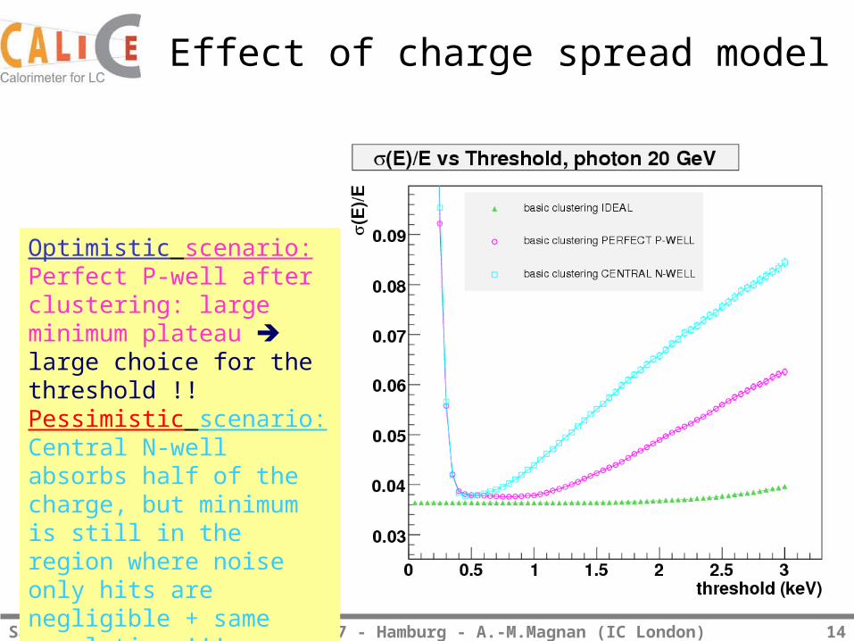
Effect of charge spread model
Optimistic scenario:Perfect P-well after clustering: large minimum plateau large choice for the threshold !!Pessimistic scenario:Central N-well absorbs half of the charge, but minimum is still in the region where noise only hits are negligible + same resolution !!!

Saturday, June 2nd, 2007
LCWS 2007 - Hamburg - A.-M.Magnan (IC London) 15
Effect of dead area and noiseafter clustering
< 6% effectThreshold > 600
eV :influence of the noise negligible
energy resolution dependant on a lot of parameters : need to measure the noise and the charge spread ! And improve the clustering, especially at high energy.

Saturday, June 2nd, 2007
LCWS 2007 - Hamburg - A.-M.Magnan (IC London) 16
Plans for the summer
• Sensor has been submitted to foundry on April 23rd, back in July.
• Charge diffusion studies with a powerful laser setup at RAL :
• 1064, 532 and 355 nm wavelength,• focusing < 2 μm,• pulse 4ns, 50 Hz repetition rate,• fully automatized
• Cosmics and source setup to provide by Birmingham and Imperial respectively.
• Work ongoing on the set of PCBs holding, controlling and reading the sensor.
• possible beam test at DESY at the end of this year.

Saturday, June 2nd, 2007
LCWS 2007 - Hamburg - A.-M.Magnan (IC London) 17
Conclusion
• Sensor v1.0 has been submitted. We aim to have first results in the coming months!
• Test are mandatory to measure the sensor charge spread and noise for digitisation simulation.
• Once we trust our simulation, detailed physics simulation of benchmark processes and comparison with analog ECAL design will be possible.

Saturday, June 2nd, 2007
LCWS 2007 - Hamburg - A.-M.Magnan (IC London) 18
Thank you for your attention

Saturday, June 2nd, 2007
LCWS 2007 - Hamburg - A.-M.Magnan (IC London) 19
Sensor layout : v1.0 submitted !
Presampler Preshaper
Type dependant area: capacitors, and big resistor or monostable
same comparator+readout logic4 diodes Ø 1.8 um
Design submitted April 23rd :

Saturday, June 2nd, 2007
LCWS 2007 - Hamburg - A.-M.Magnan (IC London) 20
THE DesignS
Low gain / High Gain Comparator
Hit Logic
Pre-Sample Pixel Analog Front End
Rst
Vrst
Preamp
PreRst
Buffer
s.f
Cfb
Cin
Buffer
s.f
Vth+Vth-
ResetSample Cstore
150ns
450ns
Self Reset
Trim&MaskSRAM SR
Hit Output
Low gain / High Gain Comparator Hit
Logic
Pre-Shape Pixel Analog Front End
Preamp
Shaper
Rst
CpreCfb
Rfb
RinCin
Vth+Vth- 150ns
Trim&MaskSRAM SR
Hit Output
Monostable
big resistor

Saturday, June 2nd, 2007
LCWS 2007 - Hamburg - A.-M.Magnan (IC London) 21
The sensor test setup
5 dead pixelsfor logic :-hits buffering (SRAM)- time stamp = BX(13 bits)- only part with clock lines.
84
pix
els
42 pixels
Data format 3 + 6 + 13 + 9 = 31 bits per hit
7 * 6 bits patternper row
Row index
1*1 cm² in total2 capacitor arrangements
2 architectures6 million transistors, 28224 pixels

Saturday, June 2nd, 2007
LCWS 2007 - Hamburg - A.-M.Magnan (IC London) 22
Beam background studies
• Done using GuineaPig• 2 scenarios studied :
• 500 GeV baseline,• 1 TeV high luminosity.
purple = innermost endcap radius500 ns reset time ~ 2‰ inactive pixels

Saturday, June 2nd, 2007
LCWS 2007 - Hamburg - A.-M.Magnan (IC London) 23
Particle Flow: work started !
• Implementing PandoraPFA from Mark Thomson : now running on MAPS simulated files.
• First plots with Z->uds @ 91 GeV in ECAL barrel gives a resolution of 35% / √E before digitisation and clustering