Embed Size (px)
Citation preview

Anisotropic optical phonon scattering of holes in cubic semiconductorsM. V. Dolguikh and R. E. Peale
Citation: Journal of Applied Physics 101, 113716 (2007); doi: 10.1063/1.2745222 View online: http://dx.doi.org/10.1063/1.2745222 View Table of Contents: http://scitation.aip.org/content/aip/journal/jap/101/11?ver=pdfcov Published by the AIP Publishing Articles you may be interested in Multiband quantum transport simulations of ultimate p-type double-gate transistors: Effects of hole-phononscattering J. Appl. Phys. 109, 073706 (2011); 10.1063/1.3556457 Band structure and optical gain of tensile-strained germanium based on a 30 band k p formalism J. Appl. Phys. 107, 013710 (2010); 10.1063/1.3279307 Physics of strain effects in semiconductors and metal-oxide-semiconductor field-effect transistors J. Appl. Phys. 101, 104503 (2007); 10.1063/1.2730561 Valence band structure of ultrathin silicon and germanium channels in metal-oxide-semiconductor field-effecttransistors J. Appl. Phys. 98, 024504 (2005); 10.1063/1.1948528 Strained silicon on SiGe: Temperature dependence of carrier effective masses J. Appl. Phys. 94, 5088 (2003); 10.1063/1.1609051
[This article is copyrighted as indicated in the article. Reuse of AIP content is subject to the terms at: http://scitation.aip.org/termsconditions. Downloaded to ] IP:
132.170.70.77 On: Fri, 30 May 2014 15:43:05
Anisotropic optical phonon scattering of holes in cubic semiconductorsM. V. Dolguikh and R. E. Pealea�
Department of Physics, University of Central Florida, Orlando, Florida 32816
�Received 5 March 2007; accepted 18 April 2007; published online 15 June 2007�
The formula for the nonpolar optical phonon scattering rate of holes in cubic semiconductors isobtained in the case of strong valence band anisotropy. The deformation potential approximation isused. A three-band, 6�6, k ·p Luttinger-Kohn representation includes states belonging to the heavy,light, and split-off bands. Mixing with the latter causes strong anisotropy in the transition matrixelements as well as in the density of final states. The derived formula is recommended for silicon,where inter- and intravalence-band scattering rates are much more strongly anisotropic and havesignificantly different values than those estimated from the usual two-band 4�4, “warped spheres”approximation that neglects the split-off band. Results for the more isotropic case of germanium arepresented for comparison. © 2007 American Institute of Physics. �DOI: 10.1063/1.2745222�
INTRODUCTION
Scattering of holes in semiconductors is induced byemission or absorption of phonons �acoustic and optical�,scattering on impurities �ionized and neutral�, and scatteringon mobile carriers. A general discussion of different scatter-ing mechanisms in p-type semiconductors is found in Refs.1–3. Rate formulas for each type of scattering have beenderived in separate papers by different authors.4–7 Clearly,any accurate description of transport or device performancemust consider all mechanisms simultaneously.
The description of each scattering phenomenon remainsincomplete, as published rate formulas have limited applica-bility. Recently, it was found necessary to develop more ac-curate formulas for hole-hole scattering7 to accurately simu-late hot-hole dynamics for p-Ge intervalence-band laserstructures at high hole concentrations.8,9 For p-Si, a potentialhot-hole terahertz gain medium,10–12 published rateformulas1,12,13 incompletely account for the strong valence-band anisotropy by neglecting the split-off band. Mixingwith this band strongly affects hole wave functions, the scat-tering matrix elements, and the density of states.
In the case of acoustic phonon scattering, the rate in-creases with temperature. Since acoustic phonons also ab-sorb terahertz radiation, they limit the maximum hot-holelaser operating temperature and duty cycle. Yet anisotropicscattering rate formulas for p-Si are lacking in the literature.Fortunately, acoustic phonon scattering can be neglected ininitial zeroth-order simulations because it is frozen out at lowtemperatures.
Ionized impurity and hole-hole scattering are importanteven at low temperature. These limit the maximum usefulconcentration of holes, and therefore the maximum achiev-able hot-hole laser gain. The recently published7 hole-holescattering rate formulas are accurate for p-Si. Impurity scat-tering is similar to hole-hole scattering, where one of theparticles is fixed.
Optical phonon scattering involves large energy ex-
change, dominates hot-carrier transport, and is responsiblefor generating population inversion in hot-hole semiconduc-tor lasers.14–16 Accurate optical phonon scattering rates are ofprimary importance for numerical simulation and optimiza-tion of intervalence-band hot-hole lasers based on p-typeGe,14–16 Si,12 GaAs,17 the negative mass cyclotron-resonancemaser,18,19 and other devices. The slow holes produced afteroptical phonon emission are especially vulnerable to hole-hole and ionized impurity scattering,7 simulation of whichdemands accurate directional distributions. Traditional for-mulas for optical phonon scattering1,12 fail in providing suchdistributions for p-Si by neglecting the split-off band and theresulting anisotropy. In this paper, the optical phonon scat-tering rate formula in the case of strong valence band aniso-tropy is obtained and discussed.
When the optical phonon energy is much smaller thanspin-orbit splitting �e.g., for Ge and GaAs�, mixing of light-and heavy-hole states with split-off band states is safely ne-glected. Then, optical phonon scattering of holes is treated inthe “warped spheres” approximation �4�4 k ·p model� withparabolic hole dispersion law.20 This simplification is suit-able for Ge and GaAs, but is inapplicable to silicon, whoseoptical phonon scattering threshold ��op=61 meV exceedsthe spin-orbit splitting �=44 meV. For silicon, mixing withthe split-off band states significantly alters the scattering rateand directional dependence. Due to the complexity of thisproblem, past authoritative treatments have elected to con-sider optical phonon scattering in all cubic semiconductors,including silicon, in a basis that excludes the split-offband.1,12 We demonstrate here the poorness of this approxi-mation for p-Si.
Drift velocities and hole current in crossed electric andmagnetic fields at low temperatures in p-Si have been calcu-lated previously,21 where authors claimed to incorporate an-isotropy of optical phonon scattering in a Monte Carlo simu-lation, but presentation or citation of a rate formula waslacking, so that it was unclear whether anisotropy in bothtransition matrix element and density of final states wereaccounted for. The transition matrix elements for some se-lected high-symmetry directions in germanium have beena�Electronic mail: [email protected]
JOURNAL OF APPLIED PHYSICS 101, 113716 �2007�
0021-8979/2007/101�11�/113716/9/$23.00 © 2007 American Institute of Physics101, 113716-1
[This article is copyrighted as indicated in the article. Reuse of AIP content is subject to the terms at: http://scitation.aip.org/termsconditions. Downloaded to ] IP:
132.170.70.77 On: Fri, 30 May 2014 15:43:05
previously calculated with inclusion of split-off bandstates,22 but results for arbitrary directions were absent. Thus,a presentation of an explicit rate formula for the general caseof optical phonon scattering in the three-band, 6�6 basis,which includes admixture of the split-off band states intolight- and heavy-hole states, appears to be lacking. This pa-per presents explicit matrix elements and total scatteringrates for arbitrary directions in cubic semiconductors in thethree-band model, together with a comparative discussion forp-Si and the more isotropic p-Ge.
An immediate application is accurate simulation of hot-hole dynamics in silicon in order to calculate and optimizegain in a p-Si terahertz laser, which has potential advantagesover the two established semiconductor terahertz lasers,namely, the p-Ge laser14 and AlGaAs-based quantum cas-cade lasers.23 Those lasers operate only up to frequencies ofabout 4.5 THz due to the onset of strong terahertz absorptionby phonons, which increases rapidly with frequency andtemperature. In contrast, Si has high transparency up to10 THz, and the temperature dependence of the lattice ab-sorption is comparatively weak.24 In addition to the bettermaterial properties for high terahertz and high temperatureoperation, a Si terahertz laser might be integrated with Sioptoelectronics.
An early Monte Carlo investigation of hot-hole lasing inp-Si reported results for orientations �B ,E�= �111,11-2� and�001, 100� only.25 A classical calculation of the volume oflight-hole accumulation in momentum space has suggestedmaximal spontaneous emission for low temperature p-Si incrossed electric and magnetic fields with orientations �001,1-10� and �11-2, 111�.26 A second Monte Carlo study12 foundterahertz amplification for �001, 100� and �001, 110�, but notfor �110, 1-10�. The first �and never repeated� experimentalobservation27 of stimulated emission in p-Si was limited tothe orientation �11-2, 1-10� and found weak signal in therange of 28–40 cm−1. Quantum mechanical calculations oflight-hole Landau level lifetimes have been performed onlyfor the orientations �110, 1-10� and �001,1-10�, for which theHamiltonian simplifies.28 A subsequent experiment,29 whichwas limited to applied field orientations �001, 100�, reportedterahertz emission above 50 cm−1. Clearly, neither theoreti-cal nor experimental possibilities have been thoroughly ex-plored, and in some cases the theoretical predictions are con-tradictory. Accurate predictions require the formulapresented here.
A possible future application of the result presented hereis simulation of hot-hole transport in p-type diamond. In dia-mond, the spin-orbit splitting �6 meV� �Ref. 1� is muchsmaller than in silicon, and the optical phonon scatteringthreshold �167 meV� �Ref. 1� is much higher. Thus, the ef-fects of valence band anisotropy are expected to be moresevere. High-field hole-drift velocity in natural diamond hasbeen measured, but the theory used a two-band Monte Carlosimulation that did not allow interpretation of the observedanisotropy.30
SCATTERING RATE FORMULA
Equation �1� presents the total transition rate with ab-sorption �upper part� or emission �lower part� of an opticalphonon. The derivation is presented in the Appendix.
P�k,�,��� =1
8�2��op� n̄��op
n̄��op+ 1
� � k�2
��E���k�,���/�k����
�Ropt�k,�;��,���d��, �1�
where
Ropt�k,�;��,��� =1
2 �,�=+,−
�es
�k�,����Hopt�es��k,��2,
�2�
with k�=k��k� ,���, and magnitude k� is subject to condition�Eq. �A16��. In Eq. �1� � is the mass density, �op the opticalphonon frequency, n̄��op
the Bose-Einstein phonon distribu-tion, E�� is the energy of the final-state band ��, and weintegrate over the direction of the final-state hole wave vec-tor k�. In Eq. �2� Hopt is the deformation potential operator,we sum over the three orthogonal phonon polarization vec-tors es,13 sum over final effective spin projections �, andaverage over initial effective spin projections . Equation �2�depends on both initial and final directions of the hole. Whenthis anisotropic squared matrix element is multiplied by theanisotropic density of the final states, as in the integrand ofEq. �1�, the anisotropy of the total scattering rate is deter-mined. The integrand of Eq. �1� defines the differential scat-tering rate of the hole with wave vector k from band � toband �� into the direction ��. Using well-known hole wavefunctions �Eqs. �A8� and �A9��, all possible intra- andintervalence-band transition rates between light and heavybands with absorption or emission of an optical phonon canbe found for an arbitrary initial hole state in the anisotropicand nonparabolic three-band model.
Optical phonon scattering in cubic semiconductors1,12,13
usually is considered in the warped spheres, 4�4, two-bandapproximation. See Eqs. �A10�–�A12� for energy spectrumand wave functions. This achieves great analytic simplifica-tion. We repeat the simplified scattering rate formula here forcompleteness. Neglecting the split-off band, Eq. �2�becomes20
Roptwarp�k,�;��,��� = dopt
2 kk���� + �
es
�E��k,es��E���k�,es� ,
�3�
where
113716-2 M. V. Dolguikh and R. E. Peale J. Appl. Phys. 101, 113716 �2007�
[This article is copyrighted as indicated in the article. Reuse of AIP content is subject to the terms at: http://scitation.aip.org/termsconditions. Downloaded to ] IP:
132.170.70.77 On: Fri, 30 May 2014 15:43:05
kk���� =
1
2�1 �
D2�k · k�� − B2k2k�2 + �3B2 − D2��i
ki2ki�
2
2��B2k�4 + C2�kx�2ky�
2 + kx�2kz�
2 + ky�2kz�
2���B2k4 + C2�kx2ky
2 + kx2kz
2 + ky2kz
2�� , �4�
and
�EH,L�k,es� = ±Ddopt�kxkyez
s + kykzexs + kxkzey
s��B2k4 + C2�kx
2ky2 + kx
2kz2 + ky
2kz2�
. �5�
The upper �lower� sign in Eq. �4� holds for intra-�inter-�valence-band transitions. The upper �lower� sign in�5� holds for the heavy-�light�-hole band. Using parabolicdispersion �Eq. �A10��, integral �1� simplifies to
P�k,�;��� =�E��k� ± ��op
25/2�2��3�op� n̄��op
n̄��op+ 1
� � m��*3/2����
�Roptwarp�k,�;��,���d��, �6�
where m�*���=�2k2 /2E��k ,�� is the effective mass of the
hole within the �th band in the � direction. The effectivemass is independent of the magnitude of k in this approxi-mation.
DISCUSSION
Squared matrix elements Eqs. �2� and �3�, and scatteringrates Eqs. �1� and �6�, were evaluated numerically using val-ues for the parameters �L ,M ,N ,� ,��op� of �−30.4, −5.7,−33.9, 290, 37� for germanium and �−6.5, −3.6, −8.7, 44, 61�for silicon �see Appendix�.31 The units for valence band pa-rameters L, M, and N are �2 /2me. The spin-orbit splitting �and optical phonon energy ��op are in meV.
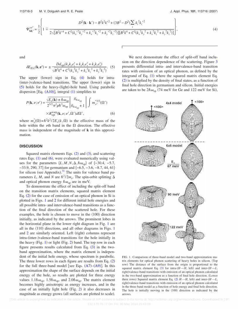
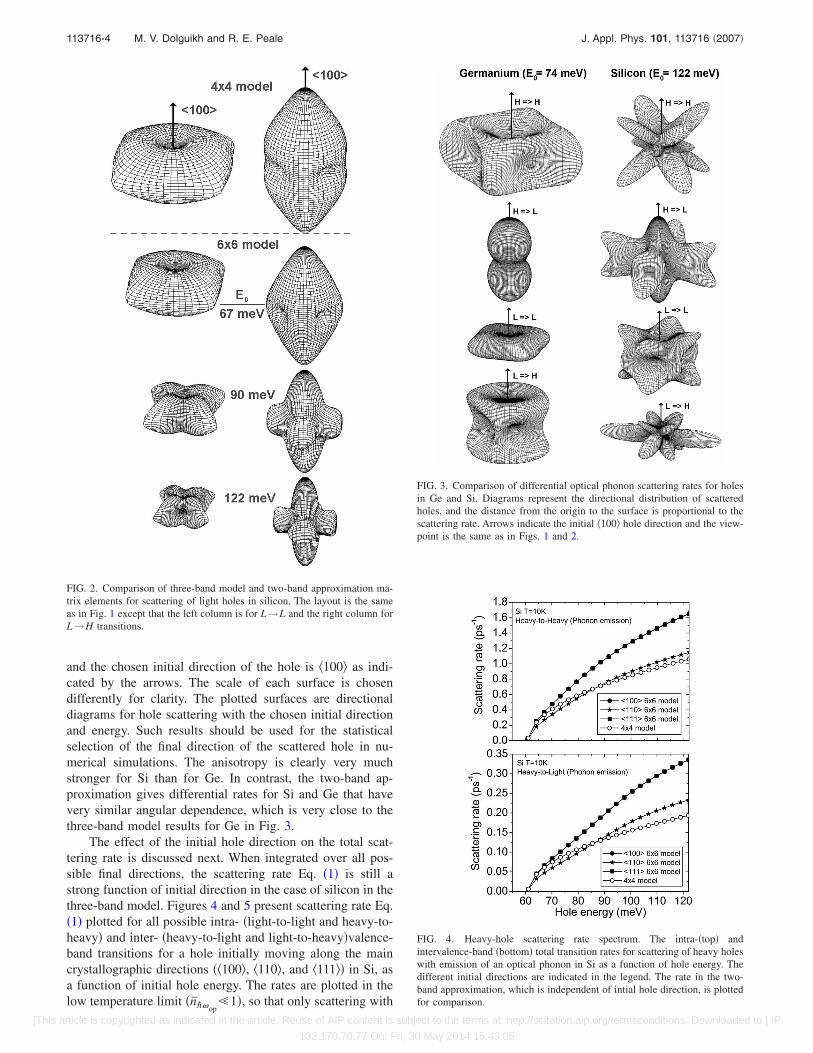
To demonstrate the effect of including the split-off bandon the transition matrix elements, squared matrix elementEq. �2� for the case of emission of an optical phonon in Si isplotted in Figs. 1 and 2 for different initial hole energies andall possible intra- and intervalence-band transitions as a func-tion of the final direction of the scattered hole. For theseexamples, the hole is chosen to move in the 100 directioninitially, as indicated by the arrows. The prominent lobes inthe horizontal plane in the lower right diagram in Fig. 1 areall in the 110 directions, and all other diagrams in Figs. 1and 2 are similarly oriented. Left �right� columns representintra-�inter-�valence-band transitions for the hole initially inthe heavy �Fig. 1� or light �Fig. 2� band. The top row in eachfigure presents results calculated from Eq. �3� in the two-band approximation, where the matrix element is indepen-dent of the initial hole energy, whose spectrum is parabolic.The three lower rows in each figure are results from Eq. �2�for the full three-band model �see Eqs. �A7�–�A9��. In thisapproximation the shape of the surface depends on the initialenergy of the hole, so results are plotted for three energyvalues 1.1��op, 1.5��op, and 2.0��op. The matrix elementbecomes highly anisotropic as energy increases, and in thecase of an initially light hole �Fig. 2� it also decreases inmagnitude as energy grows �all surfaces are plotted to scale�.
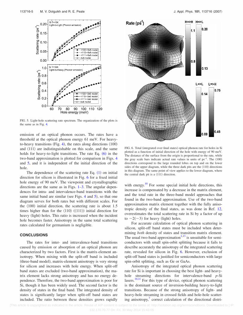
We next demonstrate the effect of split-off band inclu-sion on the direction dependence of the scattering. Figure 3presents differential intra- and intervalence-band transitionrates with emission of an optical phonon, as defined by theintegrand of Eq. �1� where the squared matrix element Eq.�2� is multiplied by the density of final states, as a function offinal hole direction in germanium and silicon. Initial energiesare taken to be 2��op �74 meV for Ge and 122 meV for Si�,
FIG. 1. Comparison of three-band model and two-band approximation ma-trix elements for optical phonon scattering of heavy holes in silicon. �Toprow� The distance of the surface from the origin is proportional to thesquared matrix element Eq. �3� for intra-�H→H, left� and inter-�H→L,right�valence-band transitions with emission of an optical phonon calculatedin the two-band approximation as a function of final hole direction. �Lowerthree rows� Squared matrix element Eq. �2� H→H, left� and inter-�H→L,right�valence-band transitions with emission of an optical phonon calculatedin the three-band model as a function of hole energy and final hole direction.The hole is initially moving in the 100 direction as indicated by thearrows.
113716-3 M. V. Dolguikh and R. E. Peale J. Appl. Phys. 101, 113716 �2007�
[This article is copyrighted as indicated in the article. Reuse of AIP content is subject to the terms at: http://scitation.aip.org/termsconditions. Downloaded to ] IP:
132.170.70.77 On: Fri, 30 May 2014 15:43:05
and the chosen initial direction of the hole is 100 as indi-cated by the arrows. The scale of each surface is chosendifferently for clarity. The plotted surfaces are directionaldiagrams for hole scattering with the chosen initial directionand energy. Such results should be used for the statisticalselection of the final direction of the scattered hole in nu-merical simulations. The anisotropy is clearly very muchstronger for Si than for Ge. In contrast, the two-band ap-proximation gives differential rates for Si and Ge that havevery similar angular dependence, which is very close to thethree-band model results for Ge in Fig. 3.
The effect of the initial hole direction on the total scat-tering rate is discussed next. When integrated over all pos-sible final directions, the scattering rate Eq. �1� is still astrong function of initial direction in the case of silicon in thethree-band model. Figures 4 and 5 present scattering rate Eq.�1� plotted for all possible intra- �light-to-light and heavy-to-heavy� and inter- �heavy-to-light and light-to-heavy�valence-band transitions for a hole initially moving along the maincrystallographic directions �100, 110, and 111� in Si, asa function of initial hole energy. The rates are plotted in thelow temperature limit �n̄��op
1�, so that only scattering with
FIG. 2. Comparison of three-band model and two-band approximation ma-trix elements for scattering of light holes in silicon. The layout is the sameas in Fig. 1 except that the left column is for L→L and the right column forL→H transitions.
FIG. 3. Comparison of differential optical phonon scattering rates for holesin Ge and Si. Diagrams represent the directional distribution of scatteredholes, and the distance from the origin to the surface is proportional to thescattering rate. Arrows indicate the initial 100 hole direction and the view-point is the same as in Figs. 1 and 2.
FIG. 4. Heavy-hole scattering rate spectrum. The intra-�top� andintervalence-band �bottom� total transition rates for scattering of heavy holeswith emission of an optical phonon in Si as a function of hole energy. Thedifferent initial directions are indicated in the legend. The rate in the two-band approximation, which is independent of intial hole direction, is plottedfor comparison.
113716-4 M. V. Dolguikh and R. E. Peale J. Appl. Phys. 101, 113716 �2007�
[This article is copyrighted as indicated in the article. Reuse of AIP content is subject to the terms at: http://scitation.aip.org/termsconditions. Downloaded to ] IP:
132.170.70.77 On: Fri, 30 May 2014 15:43:05
emission of an optical phonon occurs. The rates have athreshold at the optical phonon energy 61 meV. For heavy-to-heavy transitions �Fig. 4�, the rates along directions 100and 111 are indistinguishable on this scale, and the sameholds for heavy-to-light transitions. The rate Eq. �6� in thetwo-band approximation is plotted for comparison in Figs. 4and 5, and it is independent of the initial direction of thehole.
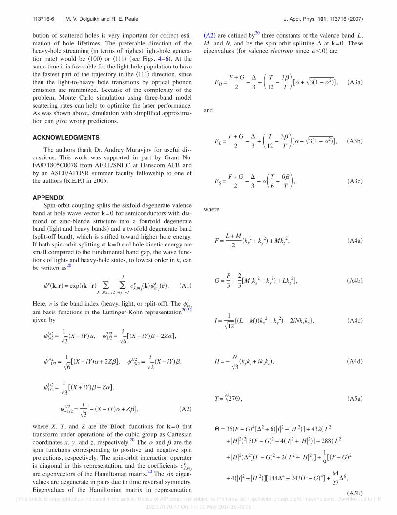
The dependence of the scattering rate Eq. �1� on initialdirection for silicon is illustrated in Fig. 6 for a fixed initialhole energy of 90 meV. The viewpoint and crystallographicdirections are the same as in Figs. 1–3. The angular depen-dences for intra- and intervalence-band transitions with thesame initial band are similar �see Figs. 4 and 5�, so that onediagram serves for both rates but with different scales. Forthe 100 initial direction, the scattering rate is about 1.5times higher than for the 110 �111� initial direction forheavy �light� holes. This ratio is increased when the incidenthole becomes faster. Anisotropy in the same total scatteringrates calculated for germanium is negligible.
CONCLUSIONS
The rates for inter- and intravalence-band transitionscaused by emission or absorption of an optical phonon arecharacterized by two factors. First is the matrix-element an-isotropy. When mixing with the split-off band is included�three-band model�, matrix-element anisotropy is very strongfor silicon and increases with hole energy. When split-offband states are excluded �two-band approximation�, the ma-trix element lacks strong anisotropy and has no energy de-pendence. Therefore, the two-band approximation is poor forSi, though it has been widely used. The second factor is thedensity of states in the final band. The integrated density ofstates is significantly larger when split-off band states areincluded. The ratio between these densities grows rapidly
with energy.10 For some special initial hole directions, thisincrease is compensated by a decrease in the matrix element,and the total rate in the three-band model approaches thatfound in the two-band approximation. Use of the two-bandapproximation matrix element together with the fully aniso-tropic density of the final states, as was done in Ref. 12,overestimates the total scattering rate in Si by a factor of upto �2��3� for heavy �light� holes.
For accurate calculation of optical phonon scattering insilicon, split-off band states must be included when deter-mining both density of states and transition matrix element.The usual two-band approximation1,13 is unsuitable for semi-conductors with small spin-orbit splitting because it fails todescribe accurately the anisotropy of the integrated scatteringrate, revealed for silicon in Fig. 6. However, exclusion ofsplit-off band states is justified for semiconductors with largespin-orbit splitting, such as Ge or GaAs.
Anisotropy of the integrated optical phonon scatteringrate for Si is important in choosing the best light- and heavy-hole streaming directions for intervalence-band p-Silasers.10,11 For this type of device, optical phonon scatteringis the dominant source of inversion-building heavy-to-lighttransitions. Because of the strong anisotropy of light- andheavy-hole streaming in crossed fields and hole-hole scatter-ing anisotropy,7 correct calculation of the directional distri-
FIG. 6. Total �integrated over final states� optical phonon rate for holes in Siplotted as a function of initial direction of the hole with energy of 90 meV.The distance of the surface from the origin is proportional to the rate, whilethe gray scale bars indicate actual rate values in units of ps−1. The 100directions correspond to the large rounded lobes on top and on the lowersides of the upper diagram, while the three dark pits are the 110 directionsin this diagram. The same point of view applies to the lower diagram, wherethe central dark pit is a 111 direction.
FIG. 5. Light-hole scattering rate spectrum. The organization of the plots isthe same as in Fig. 4.
113716-5 M. V. Dolguikh and R. E. Peale J. Appl. Phys. 101, 113716 �2007�
[This article is copyrighted as indicated in the article. Reuse of AIP content is subject to the terms at: http://scitation.aip.org/termsconditions. Downloaded to ] IP:
132.170.70.77 On: Fri, 30 May 2014 15:43:05
bution of scattered holes is very important for correct esti-mation of hole lifetimes. The preferable direction of theheavy-hole streaming �in terms of highest light-hole genera-tion rate� would be 100 or 111 �see Figs. 4–6�. At thesame time it is favorable for the light-hole population to havethe fastest part of the trajectory in the 111 direction, sincethen the light-to-heavy hole transitions by optical phononemission are minimized. Because of the complexity of theproblem, Monte Carlo simulation using three-band modelscattering rates can help to optimize the laser performance.As was shown above, simulation with simplified approxima-tion can give wrong predictions.
ACKNOWLEDGMENTS
The authors thank Dr. Andrey Muravjov for useful dis-cussions. This work was supported in part by Grant No.FA871805C0078 from AFRL/SNHC at Hanscom AFB andby an ASEE/AFOSR summer faculty fellowship to one ofthe authors �R.E.P.� in 2005.
APPENDIXSpin-orbit coupling splits the sixfold degenerate valence
band at hole wave vector k=0 for semiconductors with dia-mond or zinc-blende structure into a fourfold degenerateband �light and heavy bands� and a twofold degenerate band�split-off band�, which is shifted toward higher hole energy.If both spin-orbit splitting at k=0 and hole kinetic energy aresmall compared to the fundamental band gap, the wave func-tions of light- and heavy-hole states, to lowest order in k, canbe written as20
���k,r� = exp�ik · r� �J=3/2,1/2
�mJ=−J
J
cJ,mJ
� �k��mJ
J �r� . �A1�
Here, � is the band index �heavy, light, or split-off�. The �mJ
J
are basis functions in the Luttinger-Kohn representation20,32
given by
�3/23/2 =
1�2
�X + iY��, �1/23/2 =
i�6
��X + iY�� − 2Z�� ,
�−1/23/2 =
1�6
��X − iY�� + 2Z��, �−3/23/2 =
i�2
�X − iY�� ,
�1/21/2 =
1�3
��X + iY�� + Z��,
�−1/21/2 =
i�3
�− �X − iY�� + Z�� , �A2�
where X, Y, and Z are the Bloch functions for k=0 thattransform under operations of the cubic group as Cartesiancoordinates x, y, and z, respectively.20 The � and � are thespin functions corresponding to positive and negative spinprojections, respectively. The spin-orbit interaction operatoris diagonal in this representation, and the coefficients cJ,mJ
�
are eigenvectors of the Hamiltonian matrix.20 The six eigen-values are degenerate in pairs due to time reversal symmetry.Eigenvalues of the Hamiltonian matrix in representation
�A2� are defined by20 three constants of the valence band, L,M, and N, and by the spin-orbit splitting � at k=0. Theseeigenvalues �for valence electrons since ��0� are
EH =F + G
2−
�
3+ � T
12−
3�
T��� + �3�1 − �2�� , �A3a�
and
EL =F + G
2−
�
3+ � T
12−
3�
T��� − �3�1 − �2�� , �A3b�
ES =F + G
2−
�
3− ��T
6−
6�
T� , �A3c�
where
F =L + M
2�kx
2 + ky2� + Mkz
2, �A4a�
G =F
3+
2
3�M�kx
2 + ky2� + Lkz
2� , �A4b�
I =1
�12��L − M��kx
2 − ky2� − 2iNkxky� , �A4c�
H = −N�3
�kykz + ikxkz� , �A4d�
T = �6 27� , �A5a�
� = 36�F − G�4��2 + 6��I�2 + �H�2�� + 432��I�2
+ �H�2�2�3�F − G�2 + 4��I�2 + �H�2�� + 288��I�2
+ �H�2��2��F − G�2 + 2��I�2 + �H�2�� +1
9��F − G�2
+ 4��I�2 + �H�2���144�4 + 243�F − G�4� +64
27�6,
�A5b�
113716-6 M. V. Dolguikh and R. E. Peale J. Appl. Phys. 101, 113716 �2007�
[This article is copyrighted as indicated in the article. Reuse of AIP content is subject to the terms at: http://scitation.aip.org/termsconditions. Downloaded to ] IP:
132.170.70.77 On: Fri, 30 May 2014 15:43:05
� = cos�1
3cos−1� �− 162�3R − 8�3 − 27�F − G���F − G�2 + 6��H�2 − 2�I�2���
T3 �� , �A5c�
R = IH*2 + I*H2 =N2kz
2
6�3�− 2�L − M��kx
2 − ky2�2
− 8Nkx2ky
2� , �A5d�
� = − �F − G
2�2
− �H�2 − �I�2 −�2
9. �A5e�
Subscript labels of energies in Eq. �A3� represent heavy band�H�, light band �L�, and split-off band �S�. The positive en-ergies of holes are the negative of Eqs. �A3�.
The band constants L, M, and N needed to calculate allterms in Eqs. �A3�–�A5� are tabulated for a number of semi-conductors in Ref. 31. Light- and heavy-hole constant energysurfaces for silicon have been presented in Refs. 33 and 34.The energy surfaces of germanium are warped spheres,where the small anisotropy results from weak mixing withthe distant ��=290 meV� split-off band. In contrast, the mix-ing is much stronger for silicon, and a warped spheres de-scription is a poor choice. The strong anisotropy of energysurfaces gives strong direction dependence for the density ofhole states, which clearly affects the rates of optical phononscattering.
Once the hole spectrum E� ��=H ,L ,S� has been found,corresponding coefficients ci
� that determine the hole wavefunction can be calculated. Since all three distinct eigenval-ues �Eq. �A3�� are doubly degenerate, the sets of coefficientscJ,mJ
� for each band � are determined only to within a unitarytransformation of the degenerate functions. The coefficientscJ,mJ
�+ and cJ,mJ
�− of the two degenerate functions ��+ and ��−
for each band � may be subjected to the followingconditions:20
c3/2,3/2�− = − c3/2,−3/2
�+ *, c3/2,−3/2�− = c3/2,3/2
�+ *,
c3/2,1/2�− = c3/2,−1/2
�+ *, c3/2,−1/2�− = − c3/2,1/2
�+ *,
c1/2,1/2�− = − c1/2,−1/2
�+ *, c1/2,−1/2�− = c1/2,1/2
�+ *. �A6�
This choice of the coefficients �Eq. �A6�� is consistent withthe requirement that the eigenvalues �Eq. �A3�� of the Hamil-tonian matrix in the basis �Eq. �A2�� are doubly degenerate.The “�” and “�” labels on the band index � can be consid-ered as an “effective spin” projection . It is convenient towrite the wavefunctions �A1� as a column matrix of expan-
sion coefficients cJ,mJ
��k� in terms of Luttinger-Kohn func-
tions �Eq. �A2��,
���k,r� = exp�ik · r��
c3/2,3/2�
c3/2,1/2�
c3/2,−1/2�
c3/2,−3/2�
c1/2,1/2�
c1/2,−1/2�
� = exp�ik · r����k� ,
�A7�
where the eigenfunctions ���k� that satisfy Eq. �A6� are, for
light ��=L� and heavy ��=H� bands,
�H+
= ��EH − F��2EH + F − 3G� − 2��G − EH� − 3�H�2
2H*�EH − F + �� − 2�3HI*
I*�2EH + F − 3G + 2�� − �3H*2
0
i�2�− H*�EH − F� + �3HI*�
i�2�I*�2EH + F − 3G� − �3H*2�
� ,
�A8a�
�H−
= �0
I�2EH + F − 3G + 2�� − �3H2
− 2H�EH − F + �� + 2�3H*I
�EH − F��2EH + F − 3G� − 2��G − EH� − 3�H�2
i�2�I�2EH + F − 3G� − �3H2�
− i�2�− H�EH − F� + �3H*I�
� ,
�A8b�
�L+= �
− 2H�EL − F + �� + 2�3H*I
�EL − F��− 2EL + F + G − 2�� + 4�I�2 + �H�2
0
− I*�2EL + F − 3G + 2�� + �3H*2
i�2��EL − F��G − F� + �H�2 − 2�I�2�
i�2��3H*�EL − F� − 3HI*�
� ,
�A9a�
113716-7 M. V. Dolguikh and R. E. Peale J. Appl. Phys. 101, 113716 �2007�
[This article is copyrighted as indicated in the article. Reuse of AIP content is subject to the terms at: http://scitation.aip.org/termsconditions. Downloaded to ] IP:
132.170.70.77 On: Fri, 30 May 2014 15:43:05
�L−= �
I�2EL + F − 3G + 2�� − �3H2
0
�EL − F��2EL − F − G + 2�� − 4�I�2 − �H�2
− 2H*�EL − F + �� + 2�3HI*
i�2��3H�EL − F� − 3H*I�
− i�2��EL − F��G − F� + �H�2 − 2�I�2�
� .
�A9b�
Normalizing these vectors determines the wave functions�A1� for light- and heavy-hole valence bands in the three-band, 6�6, Luttinger-Kohn representation. Any linear com-bination of column vectors ��+ and ��− for the same bandindex � from Eqs. �A8� and �A9� is also an eigenfunction ofthe Hamiltonian matrix.
When carrier kinetic energy is small compared to thespin-orbit splitting, the wave function �A1� can be written ina reduced basis consisting of the first four Luttinger-Kohnfunctions with J=3/2, namely, �3/2
3/2, �1/23/2, �−1/2
3/2 , and �−3/23/2 . In
this two-band 4�4 approximation, the valence band is para-bolic and constant energy surfaces in momentum space arewarped spheres. The valence electron �A is negative� energyspectrum in this approximation is20
EH =F + G
2+��F − G
2�2
+ �H�2 + �I�2
= Ak2 + �B2k4 + C2�kx2ky
2 + kx2kz
2 + ky2kz
2� , �A10a�
EL =F + G
2−��F − G
2�2
+ �H�2 + �I�2
= Ak2 − �B2k4 + C2�kx2ky
2 + kx2kz
2 + ky2kz
2� , �A10b�
ES =F + G
2− � = Ak2 − � . �A10c�
Positive hole energies are the negative of Eqs. �A10�. Thewave functions �A8� and �A9� reduce to
�3/2H+��� =
1��EH − F��EH − EL��
H
EH − F
0
I*� ,
�A11�
�3/2H−��� =
1��EH − F��EH − EL��
− I
0
− �EH − F�H*
� ,
�3/2L+ ��� =
1��EL − F��EL − EH��
H
EL − F
0
I*� ,
�A12�
�3/2L− ��� =
1��EL − F��EL − EH��
− I
0
− �EL − F�H*
� ,
Numerical values for constants A, B, C, and D in Eqs. �A10�,�4�, and �5� are calculated20 from the constants L, M, and N.
Having presented the wave functions and energy spec-trum for both three-band model and two-band approxima-tion, we next consider transitions between states caused byscattering on optical phonons for each case. The opticalbranch of the phonon spectrum represents the set of har-monic oscillators describing the relative motion of the twoindividual atoms in a primitive cell. The phonon polarizationmay be taken as any set of orthogonal unit vectors.13 Thematrix of the optical deformation operator Hopt in the basis�A2� is20
Hopt�es� =2�3
dopt�exs�JyJz� + ey
s�JxJz� + ezs�JxJy�� , �A13�
where dopt=d0 /a0, the optical deformation potential d0 hasthe value1 40.3 �26.6� eV for Ge �Si�, the lattice constant a0
is 0.566 �0.543� nm for Ge �Si�, and es is the phonons-branch polarization vector. The �JiJj� are the symmetrizedproducts of the matrices of angular momentum components35
Ji and Jj in the basis �A2�,
�JiJj� =1
2�JiJj + JjJi� . �A14�
The rate of transitions from state �k ,� to state�k� ,��� with absorption �upper part� or emission �lowerpart� of an optical phonon q of branch s is
P�k,�;k�,���� =2�
�� �
2��opVc�� n̄��op
n̄��op+ 1
���k�,����Hopt�es��k,��2��E��k�
− E���k�� ± ��op� , �A15�
which is subject to the condition
k� = k��E��k� ± ��op,��,��� . �A16�
In Eq. �A15� � is the mass density, n̄��opis the Bose-Einstein
phonon distribution, Hopt is the deformation potential opera-tor, and Vc is the volume of the crystal. Integrating overfinal-state hole wave vector k�, summing over three orthogo-nal phonon polarization vectors,13 summing over final effec-tive spin projections, and averaging over initial effective spinprojections �see Eq. �2��, we obtain for the total transitionrate Eq. �1�.
113716-8 M. V. Dolguikh and R. E. Peale J. Appl. Phys. 101, 113716 �2007�
[This article is copyrighted as indicated in the article. Reuse of AIP content is subject to the terms at: http://scitation.aip.org/termsconditions. Downloaded to ] IP:
132.170.70.77 On: Fri, 30 May 2014 15:43:05
1C. Jacoboni and L. Reggiani, Rev. Mod. Phys. 55, 645 �1983�.2T. Brudevoll, T. A. Fjeldly, J. Baek, and M. S. Shur, J. Appl. Phys. 67,7373 �1990�.
3B. K. Ridley, Quantum Processes in Semiconductors �Oxford, New York,1999�.
4C. Chen, M. Dutta, and M. A. Stroscio, Phys. Rev. B 70, 075316 �2004�.5F. M. Bufler, A. Schenk, and W. Fichtner, J. Appl. Phys. 90, 2626 �2001�.6D. Chattopadhyay and H. J. Queisser, Rev. Mod. Phys. 53, 745 �1981�.7M. V. Dolguikh, A. V. Muravjov, and R. E. Peale, Phys. Rev. B 73,075327 �2006�.
8M. V. Dolguikh, A. V. Muravjov, R. E. Peale, M. Klimov, O. A. Kuz-netsov, and E. A. Uskova, J. Appl. Phys. 98, 023107 �2005�.
9M. V. Dolguikh, A. V. Muravjov, and R. E. Peale, J. Appl. Phys. 99,093106 �2006�.
10M. V. Dolguikh, A. V. Muravjov, R. E. Peale, R. A. Soref, D. Bliss, C.Lynch, and D. W. Weyburne, Proc. SPIE 5931, 310 �2005�.
11E. Bründermann, E. E. Haller, and A. V. Muravjov, Appl. Phys. Lett. 73,723 �1998�.
12E. V. Starikov and P. N. Shiktorov, Opt. Quantum Electron. 23, S177�1991�.
13P. Lawaetz, Phys. Rev. 174, 867 �1968�.14E. Bründermann, in Long Wavelength Infrared Semiconductor Lasers, ed-
ited by H. K. Choi �Wiley, New York, 2004�, pp. 279–343.15V. N. Shastin, Opt. Quantum Electron. 23, S111 �1991�.16A. A. Andronov et al., Physica B 134, 210 �1985�.17P. Kinsler and W. Th. Wenckebach, J. Appl. Phys. 90, 1692 �2001�.18V. I. Gavrilenko and Z. F. Krasil’nik, Opt. Quantum Electron. 23, S323
�1991�.19E. V. Starikov and P. N. Shiktorov, Opt. Quantum Electron. 23, S341
�1991�.20G. L. Bir and G. E. Pikus, Symmetry and Strain-Induced Effects in Semi-
conductors �Wiley, New York, 1974�.
21J. E. Dijkstra and W. Th. Wenckebach, J. Phys.: Condens. Matter 9, 10373�1997�.
22F. Szmulowicz, Phys. Rev. B 28, 5943 �1983�.23R. Kohler, A. Tredicucci, F. Beltram, H. E. Beere, E. H. Linfield, A. G.
Davies, D. A. Ritchie, R. C. Iotti, and F. Rossi, Nature �London� 417, 156�2002�.
24Peter Bruesch, Phonons: Theory and Experiments II: Experiments andInterpretation of Experimental Results (Phonons) �Springer, Berlin, 1987�,p. 57.
25A. A. Andronov, L. S. Masov, and I. M. Nefedov, in Submillimeter WaveLasers in Semiconductors Using Hot Holes, edited by A. A. Andronov�IAP AS, Gorki, 1986�, in Russian.
26V. I. Gavrilenko, E. P. Dodin, Z. F. Krasil’nik, and M. D. Chernobrovtseva,Sov. Phys. Semicond. 21, 299 �1987�.
27L. E. Vorobjev, S. N. Danilov, and V. I. Stafeev, Opt. Quantum Electron.23, S221 �1991�.
28A. V. Muravjov, R. C. Strijbos, W. Th. Wenckebach, and V. N. Shastin,Phys. Status Solidi B 205, 575 �1998�.
29E. Bründermann, E. E. Haller, and A. V. Muravjov, Appl. Phys. Lett. 73,723 �1998�.
30L. Reggiani, S. Bosi, C. Canali, and F. Nava, Phys. Rev. B 23, 3050�1981�.
31Physics of Group IV Elements and III-V Compounds, edited by O. Made-lung, Landolt-Börnstein, New Series, Group III, Pt. A, Vol. 17 �SpringerVerlag, Berlin, 1982�.
32J. M. Luttinger and W. Kohn, Phys. Rev. 97, 869 �1954�.33M. Lundstrom, Fundamentals of Carrier Transport, 2nd ed. �Cambridge
University Press, Cambridge, U.K., 2000� pp. 16–18.34J. Singh, Physics of Semiconductors and their Heterostructures �McGraw-
Hill, New York, 1993�.35L. D. Landau and E. M. Lifshitz, Quantum Mechanics (Non-relativistic
Theory), Course of Theoretical Physics �Pergamon, Oxford, 1977�, Vol. 3.
113716-9 M. V. Dolguikh and R. E. Peale J. Appl. Phys. 101, 113716 �2007�
[This article is copyrighted as indicated in the article. Reuse of AIP content is subject to the terms at: http://scitation.aip.org/termsconditions. Downloaded to ] IP:
132.170.70.77 On: Fri, 30 May 2014 15:43:05


![Review Article Prediction of Spectral Phonon Mean Free Path ...obtained the phonon relaxation times by Umklapp ( ) three-phonon scattering [ , ] and defect scattering [ ], Herring](https://img.pdfslide.us/doc/110x75/610ec2441e225c0bdc196ade/review-article-prediction-of-spectral-phonon-mean-free-path-obtained-the-phonon.jpg)