Embed Size (px)
Citation preview

© Semiconductor Components Industries, LLC, 2015
September, 2018 − Rev. 21 Publication Order Number:
AND9781/D
AND9781/D
Gen1 RangingDemonstrator Description
INTRODUCTIONThis document describes the specification and operation of the
Gen1 3D Ranging Demonstrator. This demonstrator is an engineeringprototype. Its purpose is to demonstrate SiPM technology in rangingapplications and to provide feedback for modelling of future designs.
Table 1. FUNCTIONAL SPECIFICATION
Parameter Specification Comment
Range 0.1 to 15 m
Accuracy 0.1% (TBC) < 3 mm
Resolution 1 mm (TBC) < 1 mm
Acquisition Time 400 ms
Minimum Target Reflectance 5%
Maximum Target Reflectance 90%
Max Brightness 100 klux
Ranging Method Direct ToF
Sensor MicroFC−10020−SMT
ON Semiconductor SiPMFamily
C−Series
Sensor Angle of View 1.4° 50 mm FL/25.4 mm optics
LASER Class 1
Spotting or Visible Laser Yes
Laser Wavelength 905 nm
Laser pulse width 150 ps
Laser Frequency 2 kHz to 2 MHz
Laser beam divergence 1 mrad
TDC Resolution 93.75 ps Sigma, singleshot accuracy
Power Requirements 5VDC
Power Consumption < 5 W
Interface HS USB to PC software
Form Factor PCB Board
Mounting Fixtures Optical Breadboard
Case / Housing None
Operating Temp Room Temperature
Temperature Compensation No
Board(s) Revision SiPM_Laser_Range_Finder_V2P0
www.onsemi.com
APPLICATION NOTE
Figure 1. The 3D RangingDemonstrator PCB 1.1

AND9781/D
www.onsemi.com2
SYSTEM DESIGN
System Block DiagramA block diagram of the 3D Ranging Demonstrator is
shown in Figure 2.
Figure 2. 3D Ranging Demonstrator Block Diagram (Bluetooth Not Implemented in Rev 1)
The design comprises of 6 main sections:• Optical Interface
• LASER Diode and Driver Circuitry
• SiPM Sensor (SPAD also Possible) and DiscriminatorCircuitry
• FPGA Containing TDC, Readout and CommunicationsCircuitry
• Communications Interface (HS−USB. Bluetooth not implemented in Rev 1)
• PC Software (Android also Possible)
Figure 3. Laser Collimation Tube and MountingAdapter for the Laser Diode
Optical Interface
Laser CollimationCurrently off the shelf components from Thorlabs are
used to collimate the laser diode mount the laser diode asshown below.
Table 2. COLLIMATING LENS SPECIFICATION
Manufacturer Thorlabs
Part Number C260TMD−B
Effective Focal Length 15.29 mm
Numerical Aperture 0.16
Outer Diameter 9.2 mm
Clear Aperture 5.00 mm
Working Distance @780 nm 12.43 mm
Anti−reflection Coating Range 600−1050 nm
Magnification ∞
Glass D−ZK3

AND9781/D
www.onsemi.com3
Figure 4. C260TMD−B f = 15.29 mm, NA = 0.16, Mounted Geltech Aspheric Lens, AR: 600−1050 nm
Figure 5. CAD Drawing of the C260TMD−B Lens

AND9781/D
www.onsemi.com4
Figure 6. Optical Layout for 905 nm Laser Module. Assemblies were Realized using LightPath 354330−BAspheric Lenses
Figure 7. Image Diagram at 10 m Distance for 905 nm Laser
AND9781/D
www.onsemi.com5
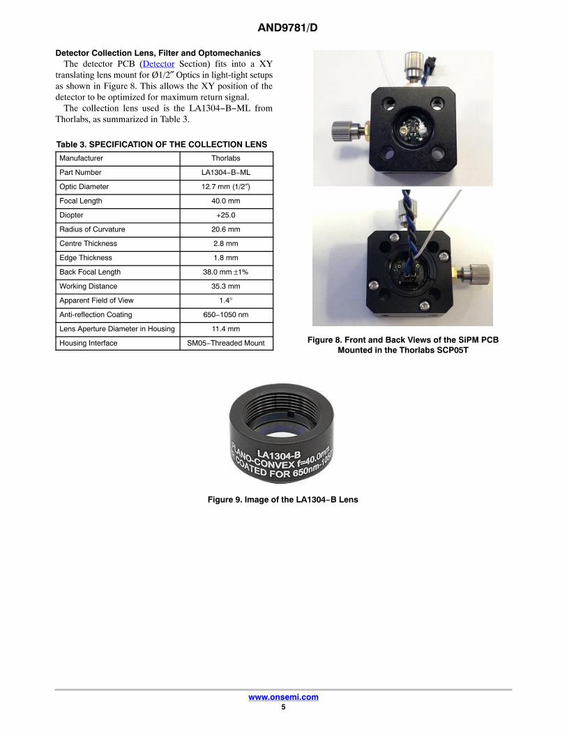
Detector Collection Lens, Filter and OptomechanicsThe detector PCB (Detector Section) fits into a XY
translating lens mount for Ø1/2″ Optics in light-tight setupsas shown in Figure 8. This allows the XY position of thedetector to be optimized for maximum return signal.
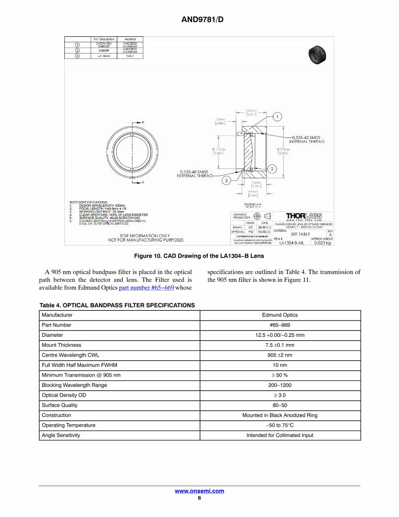
The collection lens used is the LA1304−B−ML fromThorlabs, as summarized in Table 3.
Table 3. SPECIFICATION OF THE COLLECTION LENS
Manufacturer Thorlabs
Part Number LA1304−B−ML
Optic Diameter 12.7 mm (1/2″)
Focal Length 40.0 mm
Diopter +25.0
Radius of Curvature 20.6 mm
Centre Thickness 2.8 mm
Edge Thickness 1.8 mm
Back Focal Length 38.0 mm ±1%
Working Distance 35.3 mm
Apparent Field of View 1.4°
Anti-reflection Coating 650−1050 nm
Lens Aperture Diameter in Housing 11.4 mm
Housing Interface SM05−Threaded Mount Figure 8. Front and Back Views of the SiPM PCBMounted in the Thorlabs SCP05T
Figure 9. Image of the LA1304−B Lens
AND9781/D
www.onsemi.com6
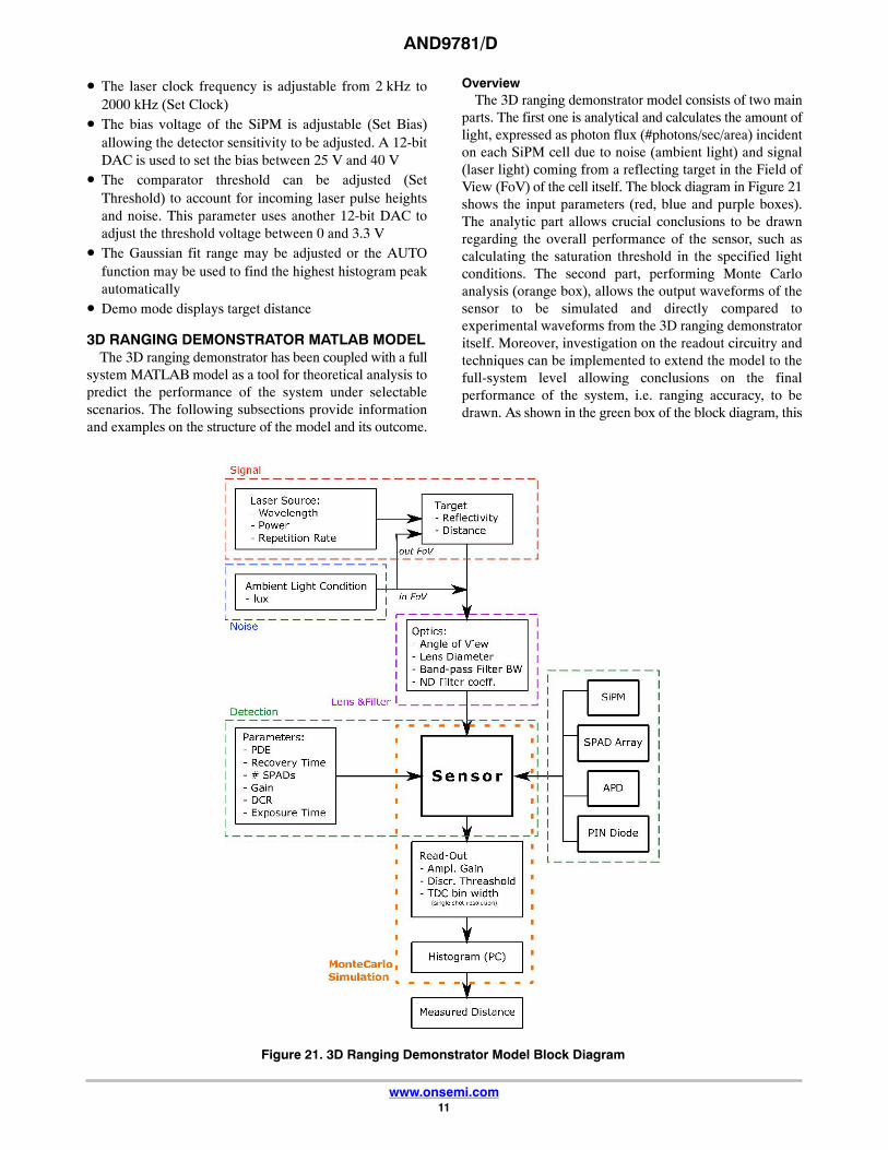
Figure 10. CAD Drawing of the LA1304−B Lens
A 905 nm optical bandpass filter is placed in the opticalpath between the detector and lens. The Filter used isavailable from Edmund Optics part number #65−669 whose
specifications are outlined in Table 4. The transmission ofthe 905 nm filter is shown in Figure 11.
Table 4. OPTICAL BANDPASS FILTER SPECIFICATIONS
Manufacturer Edmund Optics
Part Number #65−669
Diameter 12.5 +0.00/−0.25 mm
Mount Thickness 7.5 ±0.1 mm
Centre Wavelength CWL 905 ±2 nm
Full Width Half Maximum FWHM 10 nm
Minimum Transmission @ 905 nm ≥ 50 %
Blocking Wavelength Range 200−1200
Optical Density OD ≥ 3.0
Surface Quality 80−50
Construction Mounted in Black Anodized Ring
Operating Temperature −50 to 75°C
Angle Sensitivity Intended for Collimated Input

AND9781/D
www.onsemi.com7
Figure 11. Transmission Response of the 65669 Filter
The components of the optomechcanical assembly areshown with the assembled module in Figure 12.
Figure 12. Detector & Collection Lens Assembly

AND9781/D
www.onsemi.com8
Laser Diode and Driver Electronics
Table 5. LASER DIODE
Wavelength Manufacturer Part Number Package Optical Peak Power Laser Aperture
905 nm OSRAM SPLPL90 TO−185 mm Radial Plastic
Package
25 W 200 �m × 2 �m
The laser diode in Table 5 is used to illuminate the targetwith a 905 nm pulse. The laser may be pulsed at a frequencybetween 2 kHz and 2 MHz. ON Semiconductor use the laserto fire short laser pulses in the order of hundreds ofpicoseconds to give high peak power while maintaining eyesafety.
OSRAM also supply the device as a die, which is suitablefor use in high volume production design, as shown inFigure 13.
Figure 13. Osram 905 nm Laser Diode in TO−18 and Die Format
Figure 14. Top and Bottom Views of the Laser DriverPCB and Side View of the PCB Mounted to the Laser
The laser diode interfaces with a circuit board designed byON Semiconductor which pulses the laser. Images of thePCB and the PCB attached to the laser mount are shown
below. The PCB is designed to fit the form factor of theThorlabs SP02 cage plate (25 mm × 25 mm) and the laserdiode connects to the centre of the PCB.
Due to the high frequency switching of the Laser diode itis important to shield the driver circuitry from the rest of thesystem. A shielded enclosure was custom made to providethe necessary shielding. The complete assembled module isshown in Figure 15.
Figure 15. Pulsed Laser Collimation Module withEMR Shield
Laser – Sensor Field of View OverlapThe non-zero distance between the laser and the sensor
causes the laser beam and the angle to overlap starting froma minimum distance below which ranging is not possible dueto the laser not being seen by the sensor. We here calculatethe minimum ranging distance as a function of thelaser-sensor distance.
Figure 16.

AND9781/D
www.onsemi.com9
Figure 17. �AoV = 1.4� Angle of View of the Sensor
�b = 1 mrad divergence of laser beam
d = laser-sensor distance (x-axis in Figure 17)
rb(x) laser spot radius at distance x: rb(x) = x ⋅ tan �b
rs(x) sensor FoV radius at distance x: rs(x) = x ⋅ tan �AoV
Minimum partial overlap distance xmin: rs(xmin) = d − rb(xmin) (blue line)
Minimum full overlap distance xmin,full: rs(xmin,full) = d − rb(xmin,full) (red line)
For a given laser-sensor distance d, the minimum rangingdistance can be read on the graph in Figure 17.
Table 6.
Laser – Sensor Distance(d)
Minimum Ranging Distance(Full Overlap)
3 cm 128 cm
Detector and DiscriminatorA simplified block diagram of the sensor and
discriminator circuit is shown in Figure 19.
DetectorThe demonstrator design uses a MicroFC−10020−SMT
SiPM. The SiPM fast output is employed. The SiPM ismounted on a small 12.6 diameter PCB as shown inFigure 18. The PCB has two connectors, one twisted pair toprovide bias and another U.FL series coaxial connector forthe signal readout.
Figure 18. MicroFC−10020−SMT Detector Mounted atthe Centre of the Readout Board
DiscriminatorThe system uses a high power fast readout discriminator
circuit to detect the laser pulse leading edge. The fast outputof the SiPM is passed through an RF amplifier chain (2 ×ADI HMC580ST89ETR in series) to provide a signalsuitable for use with a standard comparator. The comparator(ADI ADCMP567BCPZ) has a programmable thresholdthat can be set to trigger for signal levels down to a singlephoton. The output of the comparator is fed to the input ofa pulse generator compatible with the TDC input.

AND9781/D
www.onsemi.com10
Figure 19. Discriminator Circuit Block Diagram
High SpeedPulse Generator
ComparatorGainBlocks
SiPMFast Output
To TDC
FPGA Implementing TDC, Readout and I/O CircuitryThe FPGA handles the following tasks:
• Communication with the host for configuration
• Measuring LIDAR Start-Stop sequences using internalTDC
• Saving a histogram of the LIDAR events in internal RAM
• Transferring the histogram data to the host
Due to the requirements of the TDC design it is necessaryto use an Altera CYCLONE II FPGA. The FPGA chip usedis an EP3C25F324C6.
As well as implementing a TDC within the FPGA, anexternal, low cost TDC manufactured by Texas Instruments(TDC7200), is also included. This allows the system tocompare the performance of an FPGA TDC with a moreestablished commercially available device.
The theoretical minimum LSB of the FPGA is 15.625 ps.The demonstrator employs a LSB of 93.75 ps.
The LSB of the TI device is achieved through calibration,its nominal value is 55 ps.
Communications Interface
High Speed USBThe USB interface is implemented using the FTDI
FT232H chip.
SoftwareThe PC software, written in C, is being developed for both
demonstration and research purposes. The 3D RangingDemo software plots the detected laser pulses asa histogram, performs a Gaussian fit of the data andcalculates the distance to the target using some additionalcalibration parameters.
Parameters under Software ControlThe software allows the user to optimize certain system
parameters as detailed below.
Figure 20. Demonstrator Software GUI
AND9781/D
www.onsemi.com11
• The laser clock frequency is adjustable from 2 kHz to2000 kHz (Set Clock)
• The bias voltage of the SiPM is adjustable (Set Bias)allowing the detector sensitivity to be adjusted. A 12-bitDAC is used to set the bias between 25 V and 40 V
• The comparator threshold can be adjusted (SetThreshold) to account for incoming laser pulse heightsand noise. This parameter uses another 12-bit DAC toadjust the threshold voltage between 0 and 3.3 V
• The Gaussian fit range may be adjusted or the AUTOfunction may be used to find the highest histogram peakautomatically
• Demo mode displays target distance
3D RANGING DEMONSTRATOR MATLAB MODELThe 3D ranging demonstrator has been coupled with a full
system MATLAB model as a tool for theoretical analysis topredict the performance of the system under selectablescenarios. The following subsections provide informationand examples on the structure of the model and its outcome.
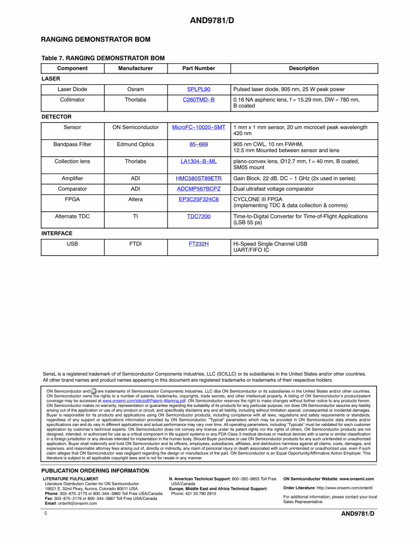
OverviewThe 3D ranging demonstrator model consists of two main
parts. The first one is analytical and calculates the amount oflight, expressed as photon flux (#photons/sec/area) incidenton each SiPM cell due to noise (ambient light) and signal(laser light) coming from a reflecting target in the Field ofView (FoV) of the cell itself. The block diagram in Figure 21shows the input parameters (red, blue and purple boxes).The analytic part allows crucial conclusions to be drawnregarding the overall performance of the sensor, such ascalculating the saturation threshold in the specified lightconditions. The second part, performing Monte Carloanalysis (orange box), allows the output waveforms of thesensor to be simulated and directly compared toexperimental waveforms from the 3D ranging demonstratoritself. Moreover, investigation on the readout circuitry andtechniques can be implemented to extend the model to thefull-system level allowing conclusions on the finalperformance of the system, i.e. ranging accuracy, to bedrawn. As shown in the green box of the block diagram, this
Figure 21. 3D Ranging Demonstrator Model Block Diagram

AND9781/D
www.onsemi.com12
part of the model takes as input the main parameters of theSiPM sensor (such as PDE, recovery time etc.) andinformation on the readout circuitry (e.g. amplifier gain,TDC resolution) can be included to evaluate the overallaccuracy of the system.
The structure of the model has been kept as simple aspossible to provide fast simulation times. Moreover, all ofthe input parameters can be easily changed to adjust themodel to the desired system configuration. Together with theSiPM sensor simulator, an APD/PIN-photo diode model hasbeen developed to offer comparisons among the maintypical sensor choices. Similarly, the read-out technique canbe replaced to compare techniques such as Leading EdgeDiscrimination (LED) or Time Correlated Single PhotonCounting (TCSPC).
ExamplesExamples of the outcome from the simulations are shown
below.
Photon Rate VS Ranging DistanceThe solar photon rate (blue line in Figure 22) is calculated
as follows:
(eq. 1)
�solar � PDsun(� � ��) � � �rlens � drange � tan �2�2
�
��1
2�d2range
� �r2lens �
�
hc
where DP_sun is the solar power density calculated byintegrating the spectral power density between � − �� and� + �� with �� being half the bandpass of the optical filteron the detector. The parameters rlens and � are respectivelythe radius and the angle of view of the lens on the detector.
The ranging distance is expressed by the parameter drangewhile � is the reflectance of the target.
The peak laser photon rate (red line) is calculated as:
(eq. 2)laser � Plaser � ��1
2�d2range
� �r2lens �
�
hc
Both photon rates are expressed in photons per secondincident on the aperture.
The two lines are compared with the SiPM saturation level(dashed red line) calculated as:
(eq. 3)�max �Ncells
PDE(�) � d
Where Ncells, PDE and �d are respectively the number ofmicrocells, the photo detection efficiency and therecovery/dead time of the SiPM. The simulated setup(described in previous sections) shows that the noise level isbelow the saturation level of the SiPM allowing rangingover all the desired distances. The decreasingsignal-to-noise at longer distances suggests the necessity ofTCSPC mode.
HistogramAn example of the output of the simulation iterated over a
programmable number of cycle (can be linked to therepetition rate of the laser pulse and the exposure time of theTDC) is shown in Figure 23. The baseline of the histogramrepresents the photons coming from the reflected solarphotons while the high pulse represents the laser pulsepositioned on the ToF. This result is achieved by simulatinga multi-event TDC (no conversion dead time, multiple eventper cycle) with a bin width of 50 ps.
Figure 22. Photon Rate (Solar and Laser) over All the Distance Range
Solar Photon RateLaser Photon Rate (Peak)SiPM Saturation Level
100 101108
109
1010
1011
1012
1013
Distance (m)
Ph
oto
n R
ate
Ambient Light: 100000 lux

AND9781/D
www.onsemi.com13
Figure 23. Example of Simulated Histogram for a Simulated 4 ns Laser Pulse
00
Time Stamp (s)
Co
un
ts
Histogram for drange = 0.77 m
500
1000
1500
2000
2500
3000
3500
4000
4500
0.2 0.4 0.6 0.8 1.0 1.2 1.4 1.6 1.8 2.0
× 10−8
Ranging ExampleBy detecting the position of the peak of the histogram due
to the laser photons, the ToF is estimated for each rangingdistance. The simulated measurements are plotted against the
expected values in Figure 24. The accuracy of themeasurement is directly connected to the number of MonteCarlo iteration steps. Longer simulations can provide betteraccuracy.
Figure 24. Ranging Curve Simulated with a Number of Cycles per Distance Step = 2000
Simulated MeasureExpected Value
100 10110−2
10−1
100
101
102
Ranging Distance (m)
Mea
sure
d D
ista
nce
(m
)
Ambient Light: 100000 lux
AND9781/D
www.onsemi.com14
RANGING DEMONSTRATOR BOM
Table 7. RANGING DEMONSTRATOR BOM
Component Manufacturer Part Number Description
LASER
Laser Diode Osram SPLPL90 Pulsed laser diode, 905 nm, 25 W peak power
Collimator Thorlabs C260TMD−B 0.16 NA aspheric lens, f = 15.29 mm, DW = 780 nm, B coated
DETECTOR
Sensor ON Semiconductor MicroFC−10020−SMT 1 mm x 1 mm sensor, 20 um microcell peak wavelength 420 nm
Bandpass Filter Edmund Optics 65−669 905 nm CWL, 10 nm FWHM, 12.5 mm Mounted between sensor and lens
Collection lens Thorlabs LA1304−B−ML plano-convex lens, Ø12.7 mm, f = 40 mm, B coated, SM05 mount
Amplifier ADI HMC580ST89ETR Gain Block, 22 dB, DC − 1 GHz (2x used in series)
Comparator ADI ADCMP567BCPZ Dual ultrafast voltage comparator
FPGA Altera EP3C25F324C6 CYCLONE III FPGA (implementing TDC & data collection & comms)
Alternate TDC TI TDC7200 Time-to-Digital Converter for Time-of-Flight Applications (LSB 55 ps)
INTERFACE
USB FTDI FT232H Hi-Speed Single Channel USB UART/FIFO IC
ON Semiconductor and are trademarks of Semiconductor Components Industries, LLC dba ON Semiconductor or its subsidiaries in the United States and/or other countries.ON Semiconductor owns the rights to a number of patents, trademarks, copyrights, trade secrets, and other intellectual property. A listing of ON Semiconductor’s product/patentcoverage may be accessed at www.onsemi.com/site/pdf/Patent−Marking.pdf. ON Semiconductor reserves the right to make changes without further notice to any products herein.ON Semiconductor makes no warranty, representation or guarantee regarding the suitability of its products for any particular purpose, nor does ON Semiconductor assume any liabilityarising out of the application or use of any product or circuit, and specifically disclaims any and all liability, including without limitation special, consequential or incidental damages.Buyer is responsible for its products and applications using ON Semiconductor products, including compliance with all laws, regulations and safety requirements or standards,regardless of any support or applications information provided by ON Semiconductor. “Typical” parameters which may be provided in ON Semiconductor data sheets and/orspecifications can and do vary in different applications and actual performance may vary over time. All operating parameters, including “Typicals” must be validated for each customerapplication by customer’s technical experts. ON Semiconductor does not convey any license under its patent rights nor the rights of others. ON Semiconductor products are notdesigned, intended, or authorized for use as a critical component in life support systems or any FDA Class 3 medical devices or medical devices with a same or similar classificationin a foreign jurisdiction or any devices intended for implantation in the human body. Should Buyer purchase or use ON Semiconductor products for any such unintended or unauthorizedapplication, Buyer shall indemnify and hold ON Semiconductor and its officers, employees, subsidiaries, affiliates, and distributors harmless against all claims, costs, damages, andexpenses, and reasonable attorney fees arising out of, directly or indirectly, any claim of personal injury or death associated with such unintended or unauthorized use, even if suchclaim alleges that ON Semiconductor was negligent regarding the design or manufacture of the part. ON Semiconductor is an Equal Opportunity/Affirmative Action Employer. Thisliterature is subject to all applicable copyright laws and is not for resale in any manner.
PUBLICATION ORDERING INFORMATIONN. American Technical Support: 800−282−9855 Toll FreeUSA/Canada
Europe, Middle East and Africa Technical Support:Phone: 421 33 790 2910
AND9781/D
SensL is a registered trademark of of Semiconductor Components Industries, LLC (SCILLC) or its subsidiaries in the United States and/or other countries. All other brand names and product names appearing in this document are registered trademarks or trademarks of their respective holders.
LITERATURE FULFILLMENT:Literature Distribution Center for ON Semiconductor19521 E. 32nd Pkwy, Aurora, Colorado 80011 USAPhone: 303−675−2175 or 800−344−3860 Toll Free USA/CanadaFax: 303−675−2176 or 800−344−3867 Toll Free USA/CanadaEmail: [email protected]
ON Semiconductor Website: www.onsemi.com
Order Literature: http://www.onsemi.com/orderlit
For additional information, please contact your localSales Representative
◊