Embed Size (px)
Citation preview

oUTLINE22-1 Semiconductor materials22-2 The P-N junction
OBJECTIVESAter studying this chapter, you should be able to:
1. Describe the difference between valence elec-trons and conduction-band electrons
2. Describe the main difference between N-typesemiconductor materials and P-typesemi-conductor materials
3. Draw a diagram of a P-N junction, includingthe depletion region
4. Draw a P-N junction that shows the polarity of ap-plied voltage for forward biasing the junction
5. Draw a P-N junction that shows the polarity of ap-plied voltage for reverse biasing thejunction
6. Explain the difference between the barrier po-tential and reverse breakdown voltagefor a P-N junction
7. Sketch the I-V curve for a typical P-N junction,showing both the forward and reverse bias partsof the curve
CHAPTER 22
Semiconductor Materialsand P-I Junctions
641

PREVIEWemiconductor devices have changed our world. Progress in electronics was once lim-ited by having to use fragile, bulky, and power-gobbling vacuum tubes instead of tiny
semiconductor devices. Transistors, diodes, integrated circuits, Complex ProgrammableLogic Devices (CPLD), and Application Specific Integrated Circuits (ASIC) are the mostcommon examples of modern-day semiconductors. Pocket calculators, desktop comput-ers, digital watches, video games, VCRs, portable electronic keyboards, DVDs, and cell-phones have been developed due to semiconductor technology. Trying to imagine aworld without the gadgets and appliances made possible with semiconductors is like try-ing to imagine modern society functioning without the automobile.
In this chapter, you get a look at the very basic inner workings that are common to allkinds of semiconductor devices. You will see why atoms of silicon are so important formaking semiconductor devices, and you will learn about a few of the other important el-ements such as germanium, arsenic, gallium, and phosphorus that are applied in semi-conductor technology. You will be introduced to the unique way that current flows throughsemiconductor materials, and you will get a first look at some graphs that are commonlyused for describing the operation of simple semiconductor devices.
KEY TERMSBarrier potentialConduction BandCovalent bondDepletion regionDiffusion currentDoping materialForward biasMajority carriers
J
Minority carriersN-type semiconductor
materialPentavabnt atomsP-N junctionP-type semiconductor
materialReverse bias
Reverse breakdownvoffaÿe
Tetravalent atomsTrivalent atomsValence electronsValence shell
22-1 Semiconductor Materials
Recall from Chapter 1 that conductors, nonconductors, and semiconductors offer differentlevels of resistance to current flow. Also remember that conductors such as copper, gold, andsilver offer little opposition to current flow, whereas good insulators such as glass, mica, andmost plastics offer a great deal of opposition to current flow. Semiconductor materials, suchas silicon combined with very small amounts of aluminum or arsenic, oppose current flow atlevels somewhere between that of the best conductors and best insulators.
In this chapter, you will discover how it is possible to adjust a semiconductor's ability topass electrical current. You will see how the same semiconductor device can be a fairly goodconductor under certain conditions and yet function as a rather good insulator under a dif-ferent set of conditions. This ability to control the conductance of semiconductor materialmakes it suitable for use in devices that can control the flow of current through a circuit andamplify electrical signals.
Review of Atomic StructureReferring to Figure 22-1, remember that the three primary particles of atoms are protons,neutrons, and electrons. The protons (positive particles) and neutrons (neutral particles) arelocated in the center, or nucleus, of the atom. The electrons (negative charges) are arrangedin orbits that surround the nucleus. In a normal, stable atom, the number of electrons in theorbits exactly equals the number of protons in the nucleus. This means that the total electri-cal charge of the atom is zero.
There is a definite limit to the number of electrons that can be included in each electron orbit,or shell. If you number the shells such that 1 is the innermost, 2 is the second from the nucleus,
CHAPTER 22 * Semiconductor Materials end P-N Junctions 643
FIGURE 22-| Atoms arecomposed of protons,neutrons, and electrons
Electrons O Neutrons Ii N+ ) Protons
Electron Energy Level
Conduction Band
Valence Band
eM
eL
eK FIGURE 22-2 Energy levelsfor atoms
Zero(Nncleus)
and so on, you can use the following formula to determine the maximum number of electrons thatcan occupy each shell, where n is the shell number.
FORMULA 22-1 2n2
Formula 22-1 shows that the innermost shell (n = 1) can contain no more than 2 elecÿons, thesecond shell (n = 2) can hold up to 8, the third (n = 3) up to 18, and so on.
Each shell represents a different energy level for the electrons that occupy it. As shown inFigure 22-2, the energy levels increase with increasing distance from the nucleus. SO youcan see that electrons located in the innermost shell possess the least amount of energÿ whilethose in the outermost shell have the greatest amount of energy. The electronic behavior ofan atom mainly depends on the relative number of electrons in its outermost shell, or valenceshell. Electrons included in the valence shell are called valence electrons.
Exposing an atom to certain outside sources of energy (notably electrical energy) givesthe valence electrons additional energy, which allows them to break away from their va-lence band and enter a conduction band. This is an important effect in electronics becauseelectrons at the conduction-band energy levels are the only ones that are free to take partin the process of electron current flow. When a valence-band electron absorbs energy, it

644 PART V • Introductory Devices and Circuits
jumps up into a conduction band. Sooner or later that same electron has to fall back downto the valence-band level, and when that happens, the electron gives up its extra load of energy--usually in the form of heat, but sometimes as a palficle of light energy.
Atomic Structures for SemiconductorsYou will soon see that the most useful semiconductor materials are those made from atomsthat have three, four, or five valence eIectrons. Atoms that normally have three valence elec-trons are called trivalent atoms, those nolÿally having four valence electrons are calledtetravalent atoms, and those normally having five outer electrons are called pentavalentatoms. Like any other atom, these are electrically neutral when they have their normal num-ber of valence elecÿons. Figure 22-3 shows examples of each of these three kinds of atoms.
The valence electrons in these semiconductoi" materials are apt to absorb energy from heatand light sources as well as electrical sources. You will find through your studies of semi-conductor devices that they respond to changes in temperature. In many instances, a rela-tively small increase in temperature can drive millions of valence electrons into conductionbands, thereby causing a dramatic decrease in electrical resistance.
These descriptions of atoms--shells, energy levels, valence electrons, and conduction-band electrons--at'e vital to your understanding of semiconductor materials and the behav-ior of semiconductor devices. Here is a brief summary of some key facts about the atomicstructures of semiconductor materials.
1. "Tri-" means three, so a trivalent atom is one that has three electrons in the valence shell.Typical trivalent semiconductor materials are boron, aluminum, gallium, and indium.
2. "Teta'a-" means foul; so a tetravalent atom is one that has four electrons in its valence shell.Typical tetravalent semiconductor materials are germanium and silicon. Silicon is by fat"the more common (which explains why the center of semiconductor technology in north-ern California is nicknamed "Silicon Valley").
3. "Penta-" meansfive, so a pentavalent atom is one that has five electrons in its valence shell.Typical pentavalent semiconductor materials are phosphorus, arsenic, and antimony.
4. Valence electrons in semiconductor materials can absorb energy and jump to conductionbands by energy sources that include electricity, heat, and light.
5. Conduction-band electrons in semiconductor materials usually emit heat energy whenthey fall back to their valence bands. In certain semiconductors, particularly gallium ar-senide, electrons dropping down to valence-band levels emit light energy.
Covalent BondsYou have already learned from an earlier lesson that matter is composed of molecules, whichare, in turn, composed of atoms that represent the basic chemical elements. Although every kindof matter in the universe is composed of atoms, there are a number of different ways atoms canbe assembled to create molecules. The materials used for making semiconductors form what isknown as a covalent bond between the individual atoms. In a covalent bond, two or more atomsshare valence electrons.
FIGURE 22-3 Trivalent,tetravalent, and pentavalentatoms
Trivalent atom Tetravalent atom Pentavalent atomAluminum Silicon Phosphorus

CHAPTER 22 * Semiconductor Materials and P-H Junctions 645
Figure 22-4 shows how a single tetravalent atom forms covalent bonds with four otheratoms of the same type. The bonds are actually three-dimensional, thus forming a crystallinemolecule, or lattice, that is shaped like a cube. A single grain of common beach sand is madeup of millions upon millions of tetravalent silicon atoms that are bonded in this fashion.
Each atom of a trivalent material forms covalent bonds with three other atoms; and by thesame token, pentavalent atoms form covalent bonds with five other identical atoms. Semi-conductors are manufactured from these trivalent, tetravalent, and pentavalent elements thatare first highly purified, then carefully combined to produce the necessary electronic effects.Because of their solid, crystalline makeup, you often hear semiconductor devices (diodes,transistors, and integrated circuits, for instance) called solid-state devices.
Practical semiconductor materials are not made from just one kind of atom, however. Mostare made from a highly purified tetravalent atom (silicon or germanium), which is combinedwith extremely small amounts of trivalent and pentavalent atoms that are called the dopingmaterial. The atoms that are chosen for this task have the ability to combine with one an-other as though they were atoms of the same element. In fact, a tetravalent atom can be"fooled" into making a covalent bond with a trivalent or pentavalent atom.
Figure 22-5 shows covalent bonds between four tetravalent atoms and one trivalent atom.The bond between the leftmost tetravalent atom and the trivatent atom is missing one elec-tron, but the covalent bonding takes place in spite of the shortage of one electron. Likewise,
®
FIGURI: 22-4 Covalentbonds for tetravalent atoms(silicon: Si)
FIGUR[ 22-5 Covalent bondsbetween a trivalent atom(boron: B) and four tetravalentatoms (silicon: Si)

646 PART V • Introductory Devices and Circuits
a pentavalent atom can bond with a tetravalent atom. As shown inFigure 22-6, this situationleaves an extra electron in the bonding arrangement.
The theory of operation of semiconductor devices rests heavily upon the notions of gaps, o1"holes, that are left when creating covalent bonds between trivalent and tetravalent atoms, andthe excess electrons that result from covalent bonds between tetravalent and pentavalent atoms.
N-Type SemiconductorsAn N-type semiconductor material is one that has an excess number of electrons. Thismeans that one out of every million or so atoms has five electrons in covalent bonds insteadof four. A block of highly purified silicon, for example, has four electrons available for co-valent bonding. Arsenic is a similar material, but has five electrons available for covalentbonding. So when a minute amount of arsenic is mixed with a sample of silicon, the arsenicatoms move into places normally occupied by silicon atoms. The "fit" is a good one exceptfor the fact that there is no place in the covalent bonds for the fifth electron. So the "fifth"electrons contributed by arsenic impurity are free to wander through the semiconductor ma-terial under external influences such as heat, light, and electrical energy.
Applying a source of electrical energy, or voltage, to a semiconductor material that hasan excess number of electrons causes those electrons to drift through the material. Thesefree electrons are repelled by the negative terminal, of the applied potential and are at-tracted to the positive terminal. See Figure 22-7. Electron flow (current) is thus established
FIGURE 22-6 Covalent bondsbetween a pentavalent atom(phosphorus: P) and fourtetravalent atoms (silicon: Si)
Electron flow(
FIGURE 22-7 Current flowthrough an N-typesemiconductor material
)
Conventionalcurrent flow
CHAPTER 22 . Semiconductor Materials and P-H Junctions 647
. through the semiconductor and any external circuitry connected to it. The current is car-ried through the semiconductor by electrons. Because electrons have a negative electricalcharge, this type of semiconductor is called an N-type (negative-type) semiconductor.
The physical principle of conduction of electrons through an N-type semiconductor isslightly different from electron flow through a good conductor. For practical purposes,though, you can think of electron flow through an N-type semiconductor as ordinary elec-tron flow through a common conductor.
P-Type Semiconductors
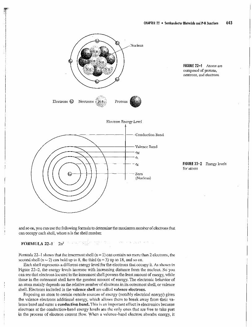
A P-type semiconductor material is one that has a shortage, or deficiency, of electrons. Aswith N-type semiconductors, the basic material is a highly purified tetravalent semiconduc-tor such as silicon or germanium. The impurity, or doping material, for a P-type semicon-ductor is a trivalent dement such as gallium or antimony. A tfivalent doping materialcontributes covalent bonds that are made of three electrons instead of four. Such bonds aremissing one electron, leaving a hole where a fourth electron would normally reside.
Every covalent bond that contains a hole is an unstable bond. This means that a little bitof external energy can cause the hole to be filled by an electron from a nearby tetravalentbond. The original hole is thus filled and its bond made more stable, but a hole is then left inthe bond that gave up its electron. See Figure 22-8. We can say that an electron moved to filla hole, but left a hole behind. It is more proper to say, however, that the hole moved. Apply-ing an external voltage to a P-type semiconductor causes holes to drift from the point of pos-itive charge to the point of negative charge. Holes, in other words, behave as positive charges.This is why such semiconductors are called P-type (positive-type) semiconductors.
More About N- and P-Type Semiconductor MaterialsA highly purified semiconductor material that has not yet been doped is known as an intrin-sic semiconductor. Once the doping material is added, the material becomes an extrinsicsemiconductor.
N-type semiconductor materials are formed by adding minute amounts of a pentavalentdement to the intrinsic semiconductor. This forces a few of the material's pentavalent atomsto provide a spare electron. The doping atoms in this instance are called donor atoms becausethey "donate" extra dectrons to the material. The charge carriers in an N-type semiconduc-tor are electrons, which are said to be the majority carriers, while holes are the minoritycarriers.
P-type semiconductors are formed by adding a tiny amount of one of the trivalent dopingmaterials. This leaves a portion of the valence shells with a,shortage of electrons (or excessholes). Because a trivalent doping material leaves holes that can subsequently accept electronsfrom other bonds, it is called an acceptor atom. The charge carriers in a P-type material are
Hole flow1.
+O O Q Q 'O 0 ,O O
@ @ ÿ @ O O O OP
,O O O O O O O ,O
Electron flow
Conventionalcurrent flow
FIGURE 22-8 CulTent flowthrough a P-typesemiconductor material

648 PART V • Introductory Devices and Circuits
positively charged holes. Holes are the majority charge carl"iers in this instance, and electronsare said to be the minority carriers.
It is important to realize that N- and P-type materials are not electrically charged. One mightsuppose that an N-type material would possess a negative charge because it contains an excessnumber of electrons; and by the same token, a P-type material would have an inherent positivecharge because of its shortage of electrons (or oversupply of positively charged holes). This isnot so. Semiconductor materials cannot supply negative and positive charges to an external cir-cuit as batteries do, for instance, r
[] IN-PROCESS LEARNING CHECK 1
Fill in the blanks as appropriate.
° Before doping (in their pure form) semiconductor materials are sometimes calledsemiconductors. Once they are doped with tiny amounts of an impurity atom, they arecalled semiconductors.
2. N-type materials are formed by doping a__ valent semiconductor material with a__ valent material. P-type materials are formed by doping a__ valentsemiconductor material with a valent material.
3. The doping atoms for N-type materials are called __ atoms because they donate extraelectrons to the covalent bonds. The doping atoms for P-type materials are called __atoms because they accept electrons that will fill the holes in the covalent bonds.
4. The majority carriers in an N-type material are __, and the minority carriers are __The majority carriers in a P-type material are __, and the minority carriers m'e __ []
22-2 The P-N Junction
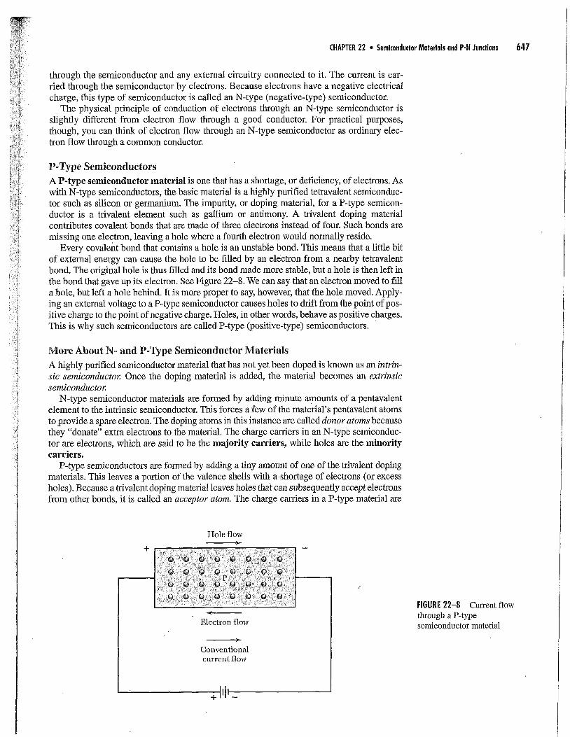
N- and P-type semiconductor materials are rarely used alone. Practical semiconductor devicesuse both materials. Semiconductor diodes, for example, use a section of N-type material thatis chemically and electrically fused to a section of P-type material (see Figure 22-9a). As youwill discover in Chapter 25, common transistors are composed of one type of semiconductorsandwiched between sections of the other type: an N-type material between two sections of Pmaterial (called a PNP transistor), or a P-type material fit between two sections of an N ma-terial (called an NPN transistor). See the examples in Figures 22-9b and 22-9c.
The region where a P-type material is chemically and electrically fused with an N-typematerial is called a P-N junction. At the P-N junction within a semiconductor device, anexcess number of electrons from the N-type material come into contact with an excess num-ber of holes from the P-type material (see Figure 22-10a). Since there are free electrons inthe N-type material near the junction of the P- and N-type materials, they are attracted tothe positive holes near the junction in the P-type material. Some electrons leave the N-typematerial to fill the holes in the P-type material. And while electrons are leaving the N-typematerial in this fashion, they leave behind positive hole charges. In other words, equal num-bers of electrons and holes flow across the P-N junction. Electrons move from the N-typematerial into the P-type material, and holes from the P-type material to the N-type material.
The result of this activity is that the N-type material now has an electron deficiency and ispositively charged because of positive ions near the P-N junction, and the P-type material hasa surplus of electrons and is negatively charged because of negative ions near the junction.This causes a potential difference near the junction that is known as the barrier potential orcontact potential (VB). See Figure 22-10b. The bah'let potential for silicon materials is 0.7 V,while that of germanium-based semiconductors is about 0.3 V.
Current flowing through the junction without an externally applied source of energy iscalled the diffusion current. Diffusion current flows only long enough to establish the bar-
CHAPTER 22 * Semiconductor Materials and P-N Junctions 649
(a)
(b)
(c)
FIGURE 22-9 Practical devices made from combinations of N- and P-type semiconductor materials:(a) diode; Co) PNP junction transistor; (c) NPN junction transistor
rier potential and maintain it when an external source of energy--such as heat, light, or anelectrical potential--is applied.
The junction region where the culTent carriers of both materials have balanced out is calledthe depletion region. This indicates that the region has been depleted of majority carriers be-cause of the diffusion current. And because there are virtually no majority carriers (excessholes or excess electrons) in this region of the semiconductor, the region acts as a good insu-lator. Study these details in Figure 22-10b.
The barrier potentialbetween the N and P layers in a semiconductor device is usually be-tween 0.3 V and 0.7 V, depending on the exact nature of the materials as well as outside in-fluences such as temperature. Although it is not possible to measure the barrier potentialdirectly, you will learn how it influences the operation of the semiconductor devices in laterchapters. Also, it is important to realize that the depletion region is quite thin, measuring onlymicrometers (millionths of a meter) across. The actual thickness of this insulating region de-pends on a number of factors, but the most significant factor for our purposes is the polarityand amount of voltage that is being applied to the semiconductor.

650 PART V * Introductory Devices and Circuits
Excess holes
!II
P
(a)
0
0 @0
N0 O
00 0 0
-ÿ0i
! 0J
I!
Excess electrons
0
P-N jl
Depletion region(very high resistance)
0 0
P
0 00N
O 0
0 0(b)
_ ÿ +
Barrier potential (VB)
FIGURE 22-10 The depletion region of a P-N junction: (a) holes and electrons recombine at thejunction; (b) the recombination of holes and electrons quickly forms the depletion region
Biasing P-N JunctionsFigure 22-11 shows a voltage source applied to the ends of a two-layer (P-N) semiconductordevice. In this instance, the positive terminal of the source is applied to the P-type region andthe negative terminal to the device's N-type region. In the first figure, Figure 22-11a, the switchis open and no potential is applied to the material. There is no current flow in the depletion re-gion. Any motion of majority carders (electrons in the N-type material and holes in the P-typematerial) is low level and random, largely because of heating effects of the surrounding air.
The instant the switch is closed, Figure 22-11b, a negative potential is applied to the N-type material and a positive potential to the P-type material. Both the electron majority car-ders in the N-type material and the hole majority carriers in the P-type material are forcedtoward the P-N junction.
If the applied voltage is greater than the contact (barrier) potential of that particular P-Njunction, the oncoming flood of majority carders eliminates the charges in the depletion re-gion. See Figure 22-11c. Positive hole charges in the depletion region are fully occupied withelectrons from the N-type material, and electrons in the depletion region are all fit into holescoming from the P-type material. The result is the total elimination of the nonconductive de-pletion region and the establishment of a steady-state current flow through the device.
A P-N junction that is conducting in this fashion--with current flow from theP-type material to the N-type material is said to be forward biased. This is possible onlywhen an external power supply is connected so that its negative supply is connected to thesemiconductor's N-type material and the positive side of the power supply is connected tothe P-type material.

CHAPTER 22 . Semiconductor Materials and P-N Junctions 651
(a) •']
P-N junction
I
f Depletion region
o 0ItO N
+
Barrier potential (VB)
Hole flow
+[ ':
! +
Barrier potential (Va)
(b) +till_
Hole flow Electron flow
I
i
--"'---- iooo0ooo
,oooooooooIi000000000!I!II
(c) +tll _
FIGURE 22=11 A forward-biased P-N junction: (a) no voltage applied to the semiconductor;(b) immediate reaction to closing the switch; (c) current flow established through the circuit
652 PART V ,, Introductory Devices and Circuits
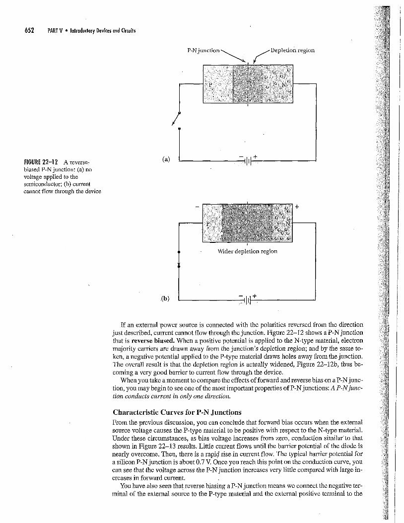
P-N junction ÿ,,,,,,ÿ S Depletion region
/|
FIGURE 22-12 Areverse-biased P-N junction: (a) novoltage applied to thesemiconductor; (b) currentcannot flow through the device
(a)
+
I
Wider depletion region
(b)
If an external power source is connected with the polarities reversed from the directionjust described, current cannot flow through the junction. Figure 22-12 shows a P-N junctionthat is reverse biased. When a positive potential is applied to the N-type material, electronmajority carriers are drawn away from the junction's depletion region; and by the same to-ken, a negative potential applied to the P-type material draws holes away from the junction.The overall result is that the depletion region is actually widened, Figure 22-12b, thus be-coming a very good barrier to current flow through the device.
When you take a moment to compare the effects of forward and reverse bias on a P-N junc-tion, you may begin to see one of the most important properties of P-N junctions: A P-N junc-tion conducts current in only one direction.
Characteristic Curves for P-N Junctions
From the previous discussion, you can conclude that forward bias occurs when the externalsource voltage causes the P-type material to be positive with respect to the N-type materialUnder these circumstances, as bias voltage increases from zero, conduction similarÿ to thatshown in Figure 22-13 results. Little current flows until the barrier potential of the diode isnearly overcome. Then, there is a rapid rise in current flow. The typical barrier potential fora silicon P-N junction is about 0.7 V. Once you reach this point on the conduction curve, youcan see that the voltage across the P-N junction increases very little compared with large in-creases in forward current.
You have also seen that reverse biasing a P-N junction means we connect the negative ter-minal of the external source to the P-type material and the external positive terminal to the
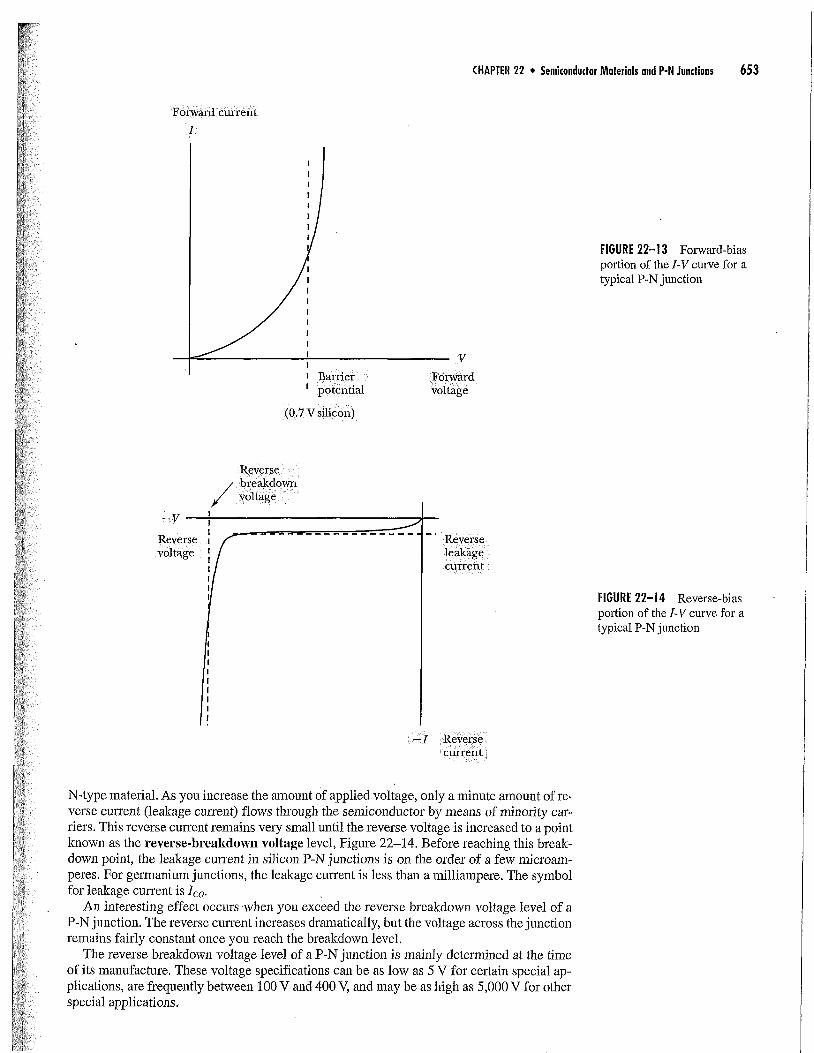
CHAPTER 22 * Semiconductor Materials and P-H Junctions 653
Forward current
I
,,
/Barrierpotential
(0.7 V silicon)
VForwardvoltage
FIGURE 22-13 Forward-biasportion of the I-V curve for atypical P-N junction
Reversebreakdownvoltage
-V
Reversevoltage
JReverseleakagecurrent
FIGURE 22-14 Reverse-biasportion of the I-V curve for atypical P-N junction
'-I Reverse
current
N-type material. As you increase the amount of applied voltage, only a minute amount of re-verse current (leakage cun'ent) flows tba'ough the semiconductor by means of minority car-riers. This reverse current remains very small until the reverse voltage is increased to a pointknown as the reverse-breakdown voltage level, Figure 22-14. Before reaching this break-down point, the leakage cmTent in silicon P-N junctions is on the order of a few microam-peres. For germanium junctions, the leakage current is less than a milliampere. The symbolfor leakage current is Ico.
An interesting effect occurs when you exceed the reverse breakdown voltage level of aP-N junction. The reverse current increases dramatically, but the voltage across the junctionremains fairly constant once yon reach the breakdown level.
The reverse breakdown voltage level of a P-N junction is mainly determined at the timeof its manufacture. These voltage specifications can be as low as 5 V for certain special ap-plications, are frequently between 100 V and 400 V, and may be as high as 5,000 V for otherspecial applications.
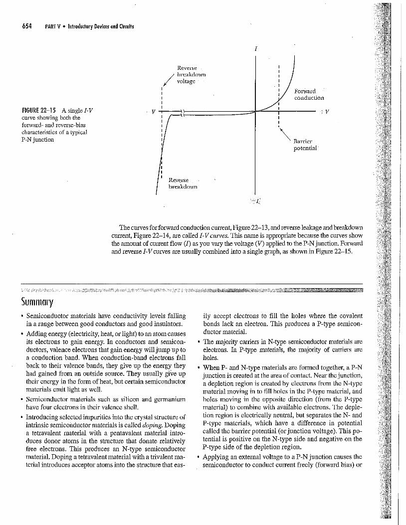
654 PART V • Introductory Devices and Circuits
FIGURE 22-15 A single I-Vcurve showing both theforward- and reverse-bias
characteristics of a typicalP-N junction
Reversebreakdownvoltage
II!!!
-V ---t------ÿ ÿ
yJ
I
//,I + VII'ÿx"X Barrier
potential
Reversebreakdown
-I
The curves for forward conduction cmlent, Figure 22-13, and reverse leakage and breakdowncurrent, Figure 22-14, are called I-V curves. This name is appropriate because the curves showthe amount of current flow (I) as you vary the voltage (V) applied to the P-N junction. Forwardand reverse I-V curves are usually combined into a single graph, as shown in Figure 22-15.
Summary• Semiconductor materials have conductivity levels falling
in a range between good conductors and good insulators.
• Adding energy (electricity, heat, or light) to an atom causesits electrons to gain energy. In conductors and semicon-ductors, valence electrons that gain energy will jump up toa conduction band. When conduction-band electrons fallback to their valence bands, they give up the energy theyhad gained from an outside source. They usually giÿce uptheir energy in the form of heat, but certain semiconductormaterials emit light as well.
• Semiconductor materials such as silicon and germaniumhave four electrons in their valence shell.
• Introducing selected impurities into the crystal structure ofintrinsic semiconductor materials is called doping. Dopinga tetravalent material with a pentavalent material intro-duces donor atoms in the structure that donate relativelyfree electrons. This produces an N-type semiconductormaterial. Doping a tetravalent material with a trivalent ma-terial introduces acceptor atoms into the structure that eas-
ily accept electrons to fill the holes where the covalentbonds lack an electron. This produces a P-type semicon-ductor material.
• The majority carriers in N-type semiconductor materials areelectrons. In P-type materials, the majority of carriers areholes.
• When P- and N-type materials are formed together, a P-Njunction is created at the area of contact. Near the junction,a depletion region is created by electrons from the N-typematerial moving in to fill holes in the P-type material, andholes moving in the opposite direction (from the P-typematerial) to combine with available electrons. The deple-tion region is electrically neutral, but separates the N- andP-type materials, which have a difference in potentialcalled the barrier potential (or junction voltage). This po-tential is positive on the N-type side and negative on theP-type side of the depletion region.
• Applying an external voltage to a P-N junction causes thesemiconductor to conduct current freely (forward bias) or
CHAPTER 22 . Semiconductor Materiols and P-N Junctions 655
act as a good insulator (reverse bias). This depends on thepolarity of the applied voltage. The junction is forward bi-ased when the applied voltage is positive to the P-type ma-terial and negative to the N-type material. On the otherhand, the junction is reverse biased when the applied volt-age is negative to the P-type material and positive to theN-type material.
• The I-V curve for a P-N junction shows that forward con-duction begins when the applied voltage reaches the junc-tion's barrier potential. The curve also shows that verylittle current flows through a P-N junction that is reversebiased until the applied voltage reaches the reverse break-down voltage level.
Formulas and Sample Calculator Sequences
FORMULA 22-1(To find maximumnumber of electronsin shell n.)
2112
shell number, [-fi], [ÿ], 2, []
EXCEL AUTOMATED FORMULAS
Helpful problem-solving tools, such as the Excel automated formulas available on the CD, allow automaticcalculations of formulas.
Review Questions1. Explain the meaning of the following terms:
a. Trivalent
b. Tetravalent
e. Pentavalent
2. List the number of valence electrons that are found in:
a. silicon.
b. arsenic.
c. gallium.
3. For an N-type semiconductor material, cite:
a. the name of the majority canSer.
b. the name of the minority carrier.
4. For a P-type semiconductor material, cite:
a. the name of the majority carrier.
b. the name of the minority cartier.
5. Indicate the typical banSer potential for:
a. a silicon P-N junction.
b. a germaninm P-N junction.
6. Which type of semiconductor material occurs when youdope a tetravalent material with a pentavalent material?
a. N-type material
b. P-type material
7. Which type of semiconductor material occurs when youdope a tetravalent material with a trivalent material?
a. N-type material
b. P-type material
8. If the electrons in a P-type material are flowing from leftto right, the holes in the same material are:
a. flowing from left to right.
b. flowing from right to left.
c. not flowing at all because they are the minority carriers.
9. Draw a P-N junction semiconductor showing an externaldc power supply connected for forward biasing.
10. Draw a P-N junction semiconductor showing an externaldc power supply connected for reverse biasing.
11. Sketch the forward-bias portion of the I-V curve for aP-N junction. Indicate the banier potential on the +V axis.
12. Sketch the reverse-bias portion of the I-V curve for a P-N junction. Indicate the breakdown voltage level onthe -V axis.

656 PART V • Introductory Devices and Circuits
Problems1. What is the maximum number of electrons that can oc-
cupy the fourth shell fi'om the nucleus in a normal atom?2. What is the maximum number of electrons that can oc-
cupy the second shell from the nucleus in a normal atom?
3. Which atomic shell has a maximum of 18 electrons?
Analysis Questions1. Explain the main difference between valence-band and 5.
conduction-band electrons.
2. Explain the main difference between intrinsic and ex-trinsic semiconductor materials. 6.
3. Describe how increasing and decreasing the amount offorward-bias voltage affects the thickness of the deple-tion region of a P-N junction,
4. Explain why the conductance of a P-N junction is muchgreater when it is forward biased than when it is reversebiased.
Explain why it can be correctly said that holes followconventional current flow and electrons follow electronflow.
Applying energy, such as heat and light, to a semicon-ductor increases carrier activity. Explain how this ac-counts for the fact that semiconductors tend to be moreconductive as their temperature rises. Compare this ef-fect with the reaction of a normal conductive materialsuch as copper.

OUTLINE23-123-223-323-423-523-623-7
DiodesDiode modelsRectifier diodesSwitching diodesSinusoJdnl inputsZener diodesOther types of diodes
OBJECTIVES
After studying this chapter, you should be able to:
1. Describe how to connect a dc source to a diodefor forward bias and for reverse bias
2. Sketch the waveforms found in an ac circuit con-sisting of a junction diode and resistor
3. Explain the function of diode clamping andclipper circuits
4. Describe the operation and specifications forzener diodes
5. Describe thepurpose of laser diodes, tunneldiodes, and varactor diodes CHAPTER 23
Diodes and Diode Circuits
657

PREVIEWou have learned that a P-NI'uncti°n normally allows current to pass in only one di-
Yrection. This normal direction of current flow occurs when the junction is forward bi-ased. This chapter introduces you to a practical application of P-N junctions in the formof semiconductor diodes.
You will discover that diodes are used for allowing or stopping electron flow and for con-trolling the direction of current flow through useful electronic circuits. Diode specificationsinclude limitations on the amount of current they can carry and the amount of reverse-biasvoltage they can withstand before breaking down. As long as you use diodes properly andwffhin their specified limits, they are very reliable devices.
Rectifier diodes are typically used for power-supply applications. Within thepower supply, you will see rectifier diodes as elements that convert ac power to dc power.
Switching diodes, on the other hand, have lower current ratings than rectifier diodes,butyou will see that switching diodes can function better in high-frequency applications andin clipping and clamping operations that deal with short-duration pulse waveforms.
Zener diodes are introduced in this chapter as a special type of P-N junction de-vice. These diodes are very commonly used as voltage-level regulators and protectorsagainst high voltage surges.
Some high-frequency ÿiode applications use tunnel diodes (used for producing high-frequency oscillators) and varactor diodes (used mainly in high-frequency tuning circuitry).
KEY TERMSAnodeCathodeClamping circuit clamperClipper circuit
Heat sinkLimiter circuitRectifier diodeSwitching diode
Tunnel diodeVaractor diodeZener diode
23-1 Diodes
The diode is constructed using the P-N junction described in Section 22-2. You have seenthat current flows easily only in one direction through a P-N junction. Figure 23-1 shows thecorrelation between the physical construction of the diode, the schematic symbol represen-tation, and the P-N junction. The arrow represents the anode---the P-type material. Thestraight bar or line represents the cathode--the N-type material. The size and shape of many
Anode
--! IN!-junction diagram
FIGURE 23-1 Adiode
Schematic symbol
Typical diode pictorial
Direction, of current flow

CHAPTER 23 . Diodes and Diode Circuits 659
diodes are similar to metal film and carbon resistors. Usually there is only one color bandnear one end of a diode that marks the cathode.
How a Diode Works in a CircuitThe diode operation will be evaluated by using the circuit shown in Figure 23-2. As the volt-age source Vs is varied from a negative voltage to a positive voltage, measurements of thecurrent flowing through the diode and the voltage dropped across the diode are taken. Plot-ting the diode current with respect to the diode voltage for this experiment provided the re-suits shown in the Figure 23-3 graph.
Prior to reflecting on the results of this experiment, we will perform the same experimentusing a resistor in place of the diode. This circuit is shown in Figure 23-4. As the voltage source
+ - -I- --
LFIGURE 23-2 Diode bias circuit
Thermalbreakdown
ForwardbiasBarriervoltage
Diode characteristic curve(nonlinear relationship)
VD
ID
Reverse lbias
Saturationcurrent
IBreakdown/J
Secondarybreakdown
FIGURE 23-3 Diodecharacteristic curve (nonlinearrelationship)
Vs ÿ-
+
N
+
NN
FIGURE 23-4 Resistor bias-circuit

660 PART V " Introductory Devices and Grcuits
FIGURE 23-5 Resistorcharacteristic curve (linearrelationship)
½
Resistor characteristic curve(linear relationship)
Vs is varied from a negative voltage to a positive voltage, measurements of the cmTent flow-ing through the resistor R1 and the voltage dropped across the resistor R1 are taken. Plottingthe results of this experiment provided the graph shown in Figure 23-5. Evaluating thisgraph, we observe a linear relationship between the voltage dropped across the resistor R1and the current flowing through the resistor RI. This relationship is known as Ohm's law. Anegative voltage dropped across the resistor resulted in the same amount of current flowingthrough the resistor as a positive voltage dropped across the resistor with the only differencebeing the direction of the current flow.
Returning to the graph that was obtained for the diode, the relationship is nonlinear.The magnitude of the current flowing through the diode with positive voltage across thediode is different from the magnitude of the current flowing through the diode with neg-ative voltage across the diode. The two different regions of operation for the diode arecalledfolward biased and reverse biased. Additional items observed from the graph arebreakdown, secondary breakdown, thermal breakdown, barrier voltage, and leakage (sat-uration) current.
A diode is forward biased when the supply voltage is greater than or equal to the diodebarrier voltage. When the diode is forward biased, current will be moving from the anode tothe cathode. The voltage dropped across the diode will be greater than or equal to the diodebattier voltage (0.3 V for germanium diodes and 0.7 V for silicon diodes). When the diode isforward biased, current is allowed to flow freely through the circuit.
A diode is reverse biased when the supply voltage is negative. When the diode is reversebiased, current will NOT be moving from the anode to the cathode. The voltage droppedacross the diode wilt be equal to the supply voltage. A very small amount of reverse leakagecurrent will flow through this circuit, but for all practical purposes, we can say that there isno current flow.
23-2 Diode Models
To effectively predict or analyze the circuits that contain diodes, an electrical model of thediode must be defined. A model is a mathematical or circuit representation of a component,device, o1" system. Through the device models, we are attempting to match the performanceof the device model to the performance of the component. The diode model used in this textis the voltage only model with the barrier voltage for silicon of 0.7 V shown in Figure 23-6.Other diode models include the ideal model and the piecewise linear model also known asthe voltage resistor model. As you compare each diode model's characteristic curve to the ac-

CHAPTER 23 . Diodes and Diode Circuits 661
a. Diode+ vD -
b. Circuit model+ vD
Folward bias
::7:ÿ
+ --
VB
Reverse bias
c. Characteristic curve
IVB
FIGURE 23-6 The voltage only diode model
tual diode characteristic curve shown in Figure 23-3 obtained from the Figure 23-2 circuit,you can observe how the models correspond to the actual performance of the diode.
Appling Kirchhoff's voltage law (KVL) to the Figure 23-2 circuit, we obtain the follow-ing equation:
Vs- Vÿ- Vÿ=O
If the supply voltage Vs and the value of the resistor R were provided, you cannot determinethe voltage dropped across the diode VD nor the voltage dropped across the resistor VR. Ohm'slaw provides you with a relationship between the voltage dropped across the resistor, the cur-rent flowing through the resistor, and the value of the resistance. Without the diode model,you are unable to calculate the voltage dropped across the diode and the current flowingthrough the diode.
The Voltage Only Diode ModelIn Figure 23-6 the diode is replaced with a closed switch and a 0.7-V battery for the forwardbiased condition (Vs > 0.7 V) and an open switch for the reverse-biased condition.
The mathematical equation for this model is:
Forward bias (Vs > 0.7 V) VD = 0.7 VID>OA
Reverse bias (Vs negative) VD = VsID=0A
You will now analyze the circuit shown in Figure 23-7.
662 PART V • Introductory Devices and Circuits
+ VD _
FIGUR[ 23-7 Example circuitn/UI[!SIM
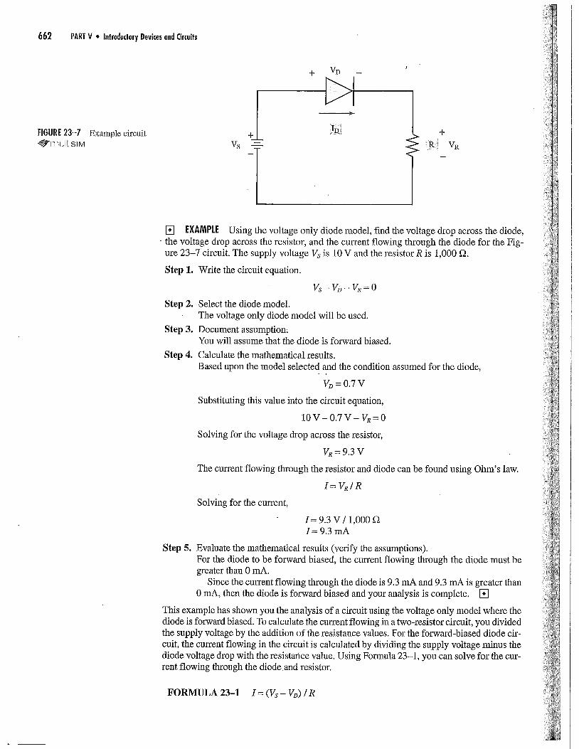
[] EXAMPLE Using the voltage only diode model, find the voltage drop across the diode,the voltage drop across the resistor, and the current flowing through the diode for the Fig-ure 23--7 circuit. The supply voltage Vs is 10 V and the resistor R is 1,000 £ÿ.
Step 1. Write the circuit equation.
Vs-- VD-- VR:O
Step 2. Select the diode model.The voltage only diode model will be used.
Step 3. Document assumption:You will assume that the diode is forward biased.
Step 4. Calculate the mathematical results.Based upon the model selected and the condition assumed for the diode,
Vÿ=0.7V
Substituting this value into the circuit equation,
10V-0.7V- VR=0
Solving for the voltage drop across the resistor,
VR=9.3V
The current flowing through the resistor and diode can be found using Ohm's law.
I=VR/R
Solving for the current,
I = 9.3 V / 1,000 ÿ2I=9.3 mA
Step 5. Evaluate the mathematical results (verify the assumptions).For the diode to be forward biased, the current flowing through the diode must begreater than 0 mA.
Since the current flowing through the diode is 9.3 mA and 9.3 mA is greater than0 mA, then the diode is forward biased and your analysis is complete. []
This example has shown you the analysis of a circuit using the voltage only model where thediode is forward biased. To calculate the current flowing in a two-resistor circuit, you dividedthe supply voltage by the addition of the resistance values. For the forward-biased diode cir-cuit, the current flowing in the circuit is calculated by dividing the supply voltage minus thediode voltage drop with the resistance value. Using Formula 23-1, you can solve for the cur-rent flowing through the diode and resistor.
FORMULA 23-1 I = (Vs - VD) / R
!
:i
tCHAPTER 23 . Dfodes and Diode Circuits 663
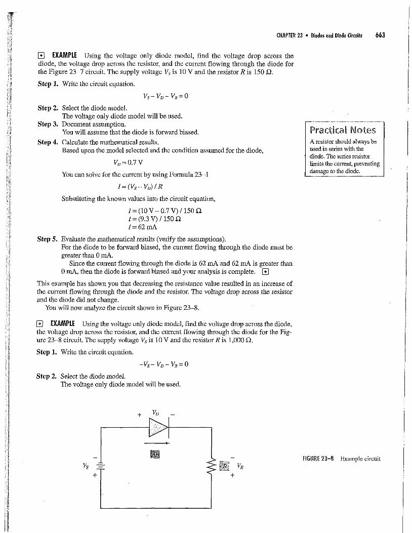
[] EXAMPLE Using the voltage only diode model, find the voltage drop across thediode, the voltage drop across the resistor, and the current flowing through the diode forthe Figure 23-7 circuit. The supply voltage Vs is 10 V and the resistor R is 150 t-2.
Step 1. Write the circuit equation.
Vs- VD- VR=O
Step 2. Select the diode model.The voltage only diode model will be used.
Step 3. Document assumption.You will assume that the diode is forward biased.
Step 4. Calculate the mathematical results.Based upon the model selected and the condition assumed for the diode,
VD=0.VV
You can solve for the current by using Formula 23-1
I = (Vs- V,,) / R
Substituting the known values into the circuit equation,
I= (lOV- 0.7 V) /150 ÿ2I = (9.3 v) ! 150 g2I=62mA
Practkal NotesA resistor should always beused in series with thediode. The series resistorlimits the current, preventingdamage to the diode.
Step 5. Evaluate the mathematical results (verify the assumptions).For the diode to be forward biased, the current flowing through the diode must begreater than 0 mA.
Since the current flowing through the diode is 62 mA and 62 mA is greater than0 mA, then the diode is forward biased and your analysis is complete. []
This example has shown you that decreasing the resistance value resulted in an increase ofthe current flowing through the diode and the resistor. The voltage drop across the resistorand the diode did not change.
You will now analyze the circuit shown in Figure 23-8.
[] EXAMPLE Using the voltage only diode model, find the voltage drop across the diode,the voltage drop across the resistor, and the current flowing through the diode for the Fig-ure 23-8 circuit. The supply voltage Vs is 10 V and the resistor R is 1,000 ÿ2.
Step 1. Write the circuit equation.
-Vs- Vÿ- VR=O
Step 2. Select the diode model.The voltage only diode model will be used.
+ VD _
FIGURE 23-8 Example circuit

664 PART V • Introductory Devices end Circuits
Step 3. Document assumption,You will assume that the diode is reverse biased.
Step 4. Calculate the mathematical results.Based upon the model selected and the condition assumed for the diode,
ID=OA
Since the Step 1 circuit equation includes only voltages and you do not loÿow thevoltage drop across the diode, an equation that relates the current to the voltagemust be provided. Using Ohm's law the voltage drop across the resistor can becalculated.
VR=IXRVR=OAx 1,000 fÿVR=0V
Substituting this value into the circuit equation,
-IOV- VD--OV=O
Solving for the voltage drop across the diode,
VD =-lOV
Step 5. Evaluate the mathematical results (verify the assumptions).For the diode to be reverse biased, the voltage across the diode must be negative.
Since the voltage across the diode is -10 V and -10 V is a negative voltage, thenthe diode is reverse biased and your analysis is complete. []
This example has shown you the analysis of a circuit using the voltage only model where thediode is reverse biased.
If you built these circuits in the lab, you will measure similar voltages and currents. Youranalysis is used to determine howthe components will perform in the ch'cuit.
PR/KIICE PROIR[ÿIS |1. What is the voltage across silicon diode Dÿ in Figure 23-9a with Vs = 12.6 VDC?
2. What is the voltage across resistor RI in Figure 23-9a?
3. What is the voltage across silicon diode D1 in Figure 23-9b with Vs = 12.6 VDC?
4. What is the voltage across, resistor R1 in Figure 23-9b?
(a) (b)
FIGURE 23-9

CHAPTER 23 ,, Diodes and Diode Circuits 665
PRACTICE PROBLEMS 2Referring to the circuit in Figure 23-10 with Vs = 76 VDC and R1 = 100 k£2:
1. What is the voltage across the silicon diode Dÿ?
2. What is the voltage across the resistor Rfl
3. How much current is flowing through the resistor RI?
General Diode RatingsDiodes have a number of ratings or specifications. Some ratings are more important than oth-ers, most often depending on the application for which the diode is designed. Typically, inmost practical cases, if you give careful attention to the most important diode ratings, the rat-ings of lesser importance automatically fall into line.
There are four diode ratings that apply in one way or another to all types of diodes andapplications.
1. Forward voltage drop, VF. As you have seen many times through earlier discussions, theforward voltage drop (or barrier potential) is the forward-conducting junction voltagelevel: about 0.3 V for germanium diodes and 0.7 V for silicon. It should be noted that en-gineers might use 0.2 V for germanium diodes and 0.6 V for silicon diodes. Experimen-tal results most commonly show a 0.68-V drop for silicon. The actual voltage dropdepends on the diode type and the current flowing through the diode.
2. Average forward current, It. This is the maximum amount of forward conduction that thediode can carry for an indefinite period of time. If the average current exceeds this value,the diode will overheat and eventually destroy itself (thermal breakdown).
3. Peak reverse voltage, VR. The peak reverse voltage (PRV) is sometimes called the reversebreakdown voltage. This is the largest amount of reverse-bias voltage the diode's junctioncan withstand for an indefinite period of time. If a reverse voltage exceeds this level, the volt-age will "punch through" the depletion layer and allow current to flow backwards throughthe diode (secondary breakdown), which usually destroys the diode. Certain special appli-cation diodes (the zener diodes) are designed to permit reverse breakdown conduction.
4. Maximum power dissipation, P. The actual diode power dissipation (Watts) is calculatedby multiplying the forward voltage drop and the forward current.
FORMULA 23-2 P = I x VD
The actual power dissipation must be less than the maximum power dissipation ratingof the diode. Exceeding the maximum power dissipation will result in thermal break-down of the diode, which is catastrophic.
Excessive forward current and exceeding reverse breakdown voltage are the most commoncauses of diode failure. In both cases, the diode gets very hot, and this heat destroys the P-N
Vs76Vÿ
100 kÿ'l
7
FIGURE 23-10 45ÿ'nquItisIM

666 PART V • Introductory Devices and Circuits
junction. Occasional "surges" of voltage or current exceeding these ratings for a very shortduration (milliseconds) may not overheat the delicate P-N junction to a point of failure, butrepeated "surges" will fatigue the junction and ultimately cause failure. To prevent this fromOCCUlTing, diodes are selected for a circuit with ratings that are two to three times the ex-pected "surge" values for that circuit.
[] IN-PROCESS LEARNING CHECK 1
Fill in the blanks as appropriate.
1. To cause conduction in a diode, the diode must be __ biased.
2. To reverse bias a diode, connect the negative source to the __ and the positive sourcevoltage to the __
3. The anode of a diode corresponds to the ___-type material, and the cathode correspondsto the __-type material.
4. The forward conduction voltage drop across a silicon diode is approximately __ V.
5. When a diode is reverse biased in a circuit, it acts like a(n) __ (open, closed) switch.
6. When the diode is biased, there will beno current flow through the diode.
7. When a diode is connected in series with a resistor, the voltage across the resistor is verynearly equal to the dc source voltage when the diode is __ biased.
8. The four most general diode ratings are ...... and___[]
23-3 Rectifier Diodes
Rectifier diodes are used where it is necessary to change an alternating-current power sourceinto a direct-current power source. Rectifier diodes are the most rugged and durable of thesemiconductors in the junction diode family. They are especially noted for theft" large aver-age forward current and reverse breakdown voltage ratings. Figure 23-11 lists some commonrectifier diode specifications.
Part Identification Code
1N4001
1N4002
1N4003
1N4004
1N4007
1N5400
1N5401
1N5402
1N5404
1N5408
Breakdown Voltage
vÿ(v)
50
100
200
400
1000
Power RatingP(W)
25W
2.5W
2.5W
2.5W
2.5W
50
100
2OO
4OO
!o0o
6.25W
6.25W
6.25W
6.25W
6.25W
FIGURE 23-11 Typical ratings for rectifier diodes
t
CHAPTER 23 ,, Diodes and Diode Circuits 667
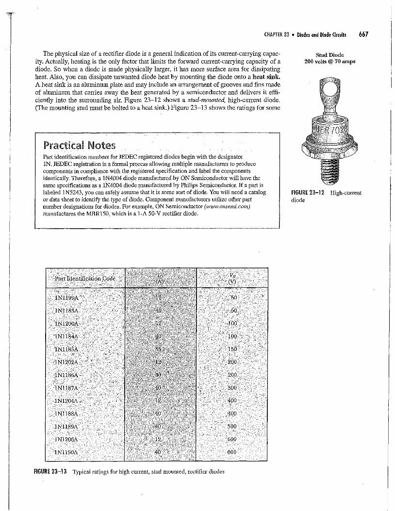
The physical size of a rectifier diode is a general indication of its current-carrying capac-ity. Actually, heating is the only factor that limits the forward current-carrying capacity of adiode. So when a diode is made physically larger, it has more surface area for dissipatingheat. Also, you can dissipate unwanted diode heat by mounting the diode onto a heat sink.A heat sink is an aluminum plate and may include an arrangement of grooves and fins madeof aluminum that carries away the heat generated by a semiconductor and delivers it effi-ciently into the surrounding air. Figure 23-12 shows a stud-mounted, high-current diode.(The mounting stud must be bolted to a heat sink.) Figure 23-13 shows the ratings for some
Stud Diode200 volts @ 70 amps
Practkal NotesPart identification numbers for JEDEC registered diodes begin with the designatorIN. JEDEC registration is a formal process allowing multiple manufacturers to producecomponents in compliance with the registered specification and label the componentsidentically. Therefore, a 1N4004 diode manufactured by ON Semiconductor will have thesame specifications as a 1N4004 diode manufactured by Philips Semiconductor. If a part islabeled 1N5243, you can safely assume that it is some sort of diode. You will need a catalogor data sheet to identify the type of diode. Component manufacturers utilize other partnumber designations for diodes. For example, ON Semiconductor (www.onsemi.com)manufactures the MBR150, which is a 1-A 50-V rectifier diode.
FIGUR[ 23-12 High-currentdiode
Part Identification Code
1Nl199A
1N1183A
1N1200A
1Nl184A
1N1185A
1N1202A
1Nl185A
1Nl187A
IN1204A
1Nl188A
1Nl189A
1N1206A
1Nll90A 40 :
VR(V)
5O
50
100
100
150
2O0
200
300
400
400
5OO
60O
6OO
FIGURE 23-13 Typical ratings for high current, stud mounted, rectifier diodes
668 PART V * Introductory Devices and Circuits
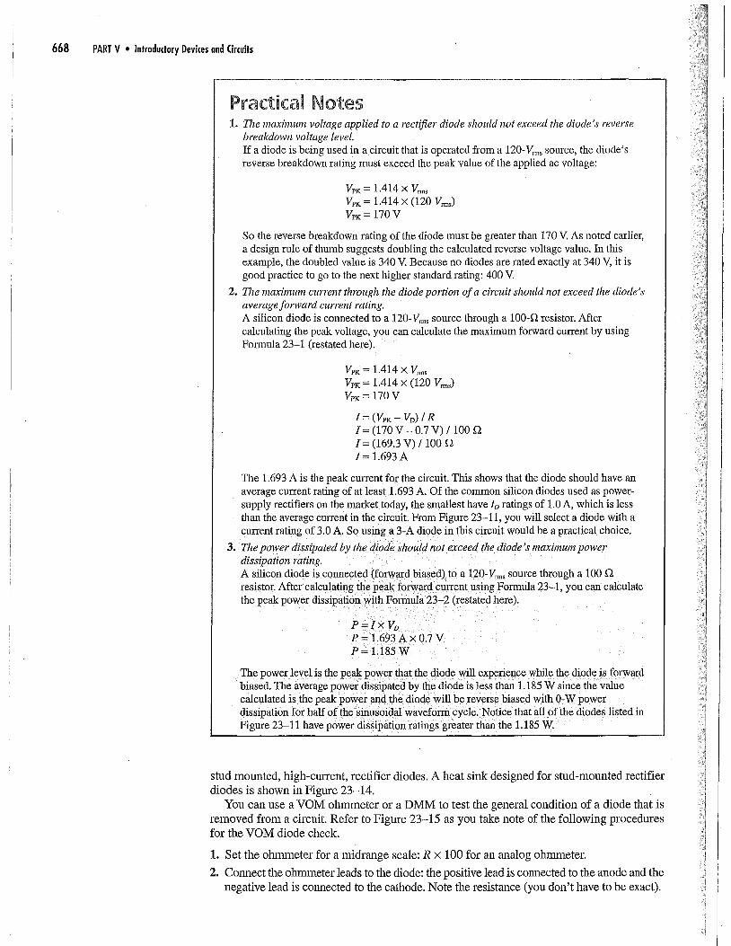
Practical Notes1, The maximum voltage applied to a rectifier diode should not exceed the diode's reverse
breakdown voltage level.If a diode is being used in a circuit that is operated from a 120-Vrmÿ source, the diode'sreverse breakdown rating must exceed the peak value of the applied ac voltage:
VpK = 1.414 X VÿmÿVpK = 1.414 X (120 Vÿm0VVK = 170 V
2,
So the reverse breakdown rating of the diode must be greater than 170 V. As noted earlier,a design rule of thumb suggests doubling the calculated reverse voltage value. In thisexample, the doubled value is 340 V. Because no diodes are rated exactly at 340 V, it isgood practice to go to the next higher standard rating: 400 V.
The maximum current through the diode portion of a circuit should not exceed the diode'saverage forward current rating.A silicon diode is connected to a 120-Vrr,ÿ source through a 100-D resistor. Aftercalculating the peak voltage, you can calculate the maximum forward current by usingFormula 23-1 (restated here).
VpK = 1.414 × VÿmsVpK = 1.414 X (120 Vrms)VpK = 170 V
I = (VpK- VD) /RI = (170 V - 0.7 V) / 100 ÿ2I = (169.3 V) / 100I = 1.693 A
3.
The 1.693 A is the peak current for the circuit. This shows that the diode should have anaverage current rating of at least 1.693 A. Of the common silicon diodes used as power-supply rectifiers on the market today, the smallest have Io ratings of 1.0 A, which is lessthan the average current in the circuit. From Figure 23-11, you will select a diode with acurrent rating of 3.0 A. So using a 3-A diode in this circuit would be a practical choice.
The power dissipated by the diode should not exceed the diode's maximum powerdissipation rating.A silicon diode is connected (forward biased) to a 120-Vÿmÿ source through a 100 fÿresistor. After calculating the peak forward current using Formula 23-1, you can calculatethe peak power dissipation with Formula 23-2 (restated here).
P=IX VDP = 1.693 A X 0.7 VP= 1.185W
The power level is the peak power that the diode will experience while the diode is forwardbiased. The average power dissipated by the diode is less than 1.185 W since the valuecalculated is the peak power and the diode will be reverse biased with 0-W powerdissipation for half of the sinusoidal waveform cycle. Notice that all of the diodes listed inFigure 23-11 have power dissipation ratings greater than the 1.185 W.
J1!
stud mounted, high-current, rectifier diodes. A heat sink designed for stud-mounted rectifierdiodes is shown in Figure 23-14.
You can use a VOM ohmmeter or a DMM to test the general condition of a diode that isremoved from a circuit. Refer to Figure 23-15 as you take note of the following proceduresfor the VOM diode check.
1. Set the ohmmeter for a midrange scale: R x 100 for an analog ohmmeter.
2. Connect the ohmmeter leads to the diode: the positive lead is connected to the anode and thenegative lead is connected to the cathode. Note the resistance (you don't have to be exact).

CHAPTER 23 . Diodes and Diode Circuits 669
FIGURE 23-14 Heat sink
..... ::. .................
FIGURE 23-15 Ohmmetertests for diodes
Forward biasLow forward resistance
Reverse biasHigh reverse resistance
3. Reverse the ohmmeter connections to the diode so that the positive lead is now connectedto the cathode and the negative lead is connected to the anode. Note the resistance (again,you don't have to be exact).
If the diode is in good working order, you should find a much higher resistance when thediode is reverse biased than when it is forward biased. The diode is defective (usuallyshorted) when the forward and reverse ohmmeter readings are in the same general range.
If a DMM is used, you would use the device's "diode test" circuit rather than the ohm-meter function.
1. Set the DMM for the diode test mode.
2. Connect the DMM leads to the diode: the positive lead is connected to the anode and thenegative lead is connected to the cathode. Note the reading. Most digital multimeters(DMM) display the forward voltage drop with 1 to 3 mA of current flow. If the DMM dis-plays 0 V or OL is indicated, then the diode is defective.
3. Reverse the DMM connections to the diode so that the positive lead is now connected to thecathode and the negative lead is connected to the anode. Most DMMs should display an overlimits or overvoltage (OL) indicating that the diode is reverse biased. If any other reading isindicated, then the diode is defective.
23-4 Switching Diodes
A second type of diode is designed for high frequency and small signal applications such asthe circuits commonly found in communications equipment and in computers. They are alsoused in circuits where diode action has to take place reliably in a very short period. These

670 PART V ° Introductory Devices and Circuits
diodes, called switching diodes, usually have low current and voltage ratings, and they areno larger than the smaller rectifier diodes. (Most switching diodes are less than a quarter-inchlong, and the surface mount versions are only about 0.1 inch square.) Figure 23-16 showsthe specifications for several JEDEC registered switching diodes.
Switching diodes are made in such a way that they can respond very quickly to changesin the polarity of the signal applied to them. This reverse recovely time (try) rating is lessthan 50 ns (nanoseconds), or 50 × 10-9 s. This means the diode will recover from a reverse-voltage state and begin forward conducting within 50 ns. By contrast, the bulkier con-struction of rectifier diodes gives them a longer recovery time. A typical reverse recoverytime for a rectifier diode is on the order of 30 msec, which is 600 times longer than a typ-ical switching diode.
23-5 Sinusoidal Inputs
Diode Clipper CircuitsA diode clipper circuit removes the peaks from an input waveform. There are a number ofreasons for using such a circuit. For example, a diode clipper can be used in waveshaping cir-cuits to remove unwanted spikes. Diode clippers are also called limiter circuits.
There are two basic kinds of diode clipper circuits: series and shunt (parallel) clippers. Ina series diode clipper, the diode is connected in series between the circuit's input and outputterminals. In a shunt diode clipper, the diode is connected in parallel between the input andoutput terminals of the circuit.
Series Diode ClipperFigureÿ 23-17 and Figure 23-18 show a pair of series diode clippers. The only differencebetween the two is that the circuit in Figure 23-17 clips off the negative portion of the in-put waveform, while the Figure 23-18 circuit clips off the positive portion. The clippingaction of these series clippers works according to the principle that the diode will conductcurrent only when it is forward biased. In Figure 23-17, the diode is forward biased on thepositive portion of the input waveform when the generator voltage exceeds the diode bar-tier voltage (0.7 V for silicon diodes), thereby allowing the positive portion of the wave-form to be duplicated across the output resistor. When the generator voltage is less than thediode barrier voltage, which includes the waveform's negative half-cycle, the diode is re-verse biased and cannot pass that part of the input waveform to the output resistor. In Fig-ure 23-18, the diode is turned around so that it is forward biased when the negative portionof the input waveform is greater than the diode barrier voltage.
FIGIJR[ 23-16 Typical ratingsfor switching diodes
PartIdentification
1N4150
1N4153
1N4151
1N4148
1N914B
1N914A
1N914
1N4448
........ ....
? :75:
..... 75
0.74 V @ 10 mA
0.88 V @ 20 mA
1.00V@ 50mA
1.00 V @ 10mA
0.72 V @ 5 liE&
1.00V@ 20mA
1.00 V @ 10 nab.
0.72V@ 5mA
5ov:
25 nA @ 20v!,: ?- :
25 nA@ 20 V
25 nA @ 20V
t=(ns)
4
2
2
4
4
4
4
4
CHAPTER 23 . Diodes and Diode Circuits 671
+ ÿ _
...F
R VouT
(a) -ÿ'muItiSlM
15
10
5
0
-5
-10
\ I //I y //X\ .... ,/ /
t (sec)
-15
(b)
Vout
15
10
5
o
-5
-10
// ",\\
/ \ / \9.3V
t (sec)
-15
(c)FIGURE 23-17 Negative clipper (series): (a) schematic; (b) input waveform; (c) output waveform
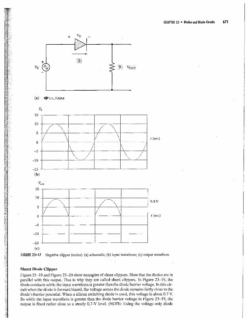
Shunt Diode ClipperFigure 23-19 and Figure 23-20 show examples of shunt clippers. Note that the diodes are inparallel with this output. That is why they are called shunt clippers. In Figure 23-19, thediode conducts while the input waveform is greater than the diode barrier voltage. In this cir-cuit when the diode is forward biased, the voltage across the diode remains fairly close to thediode's barrier potential. When a silicon switching diode is used, this voltage is about 0.7 V.So while the input waveform is greater than the diode barrier voltage in Figure 23-19, theoutput is fixed rather close to a steady 0.7-V level. (NOTE: Using the voltage only diode

672 PART V • Introductory Devices and Circuits
+
+
iÿ' VOUT
(a)
Vs
15
0
-5
-10
lO
5 //
,/
\\ /
/
//
\ /t (ÿec)
-15
(b)gout
15
5
0
-5
-10
10
\ / \ /t (sec)
-9.3 V
-15
(c)
FIGURE 23-18 Positive clipper (series): (a) schematic; (b) input waveform; (c) output waveform
model, the diode voltage is fixed at 0.7 V. Using the voltage resistor diode model, the diode- voltage will increase slightly from the 0.7 V.) When the input waveform goes below the diode
barrier potential voltage, the diode is then reverse biased and the entire negative half-cycleappears across the diode and output of the circuit. So in this case, the positive half-cycle iseffectively clipped from the input waveform.
The simple shunt clipper in Figure 23-20 is identical with the Figure 23-19 circuit except thatthe diode is reversed in its place across the output. The input waveform is clipped, or limited,during the negative portion of the input cycle. The diode is reverse biased during the positive

CHAPTER 23 . Diodes and Diode Circuits 673
+
+ ½
V4-ii i!
+ +
VD VOUT
(a)
Vs
15
10
5
0
-5
-10
/ \ / \\ /
t (sec)
-15
(b)Vout
15
lO
5
o
-5
-10
\ / \ /0.7V
t (sec)
-lO V
-15
(c)
FIGURE 23-19 Positive diode clipper (shunt): (a) schematic; (b) input waveform;(c) output waveform ÿmultisIM
half-cycle, so that is the portion of the input waveform that appears at the output terminals of thecircuit. The addition of a load resistance or the input impedance of another component willchange the output waveform.
Biased Diode ClippersAn interesting variation of the basic diode clipping action is to bias the diodes purposely sothey limit the waveform to a value other than zero. Examples of biased diode clippers areshown in Figure 23-21 and in Figure 23-22.

674 PART V • Introductory Devices and Circuits
Vs
+
N
+ ½
(a)
Vs
15
10;p/
5 /
0
-5
-10
-15
(b)Vout
15
10
5
0
-5
-10
-15
(c)FIGURE 23-20wave form
\//
\ /
.¢
////
///
'\\,
\\
//
\\ //
\,
t (sec)
/
/ / \/ //
IOV
t (sec)
-0.TV
Negative diode clipper (shunt): (a) schematic; (b) input waveform; (c) output
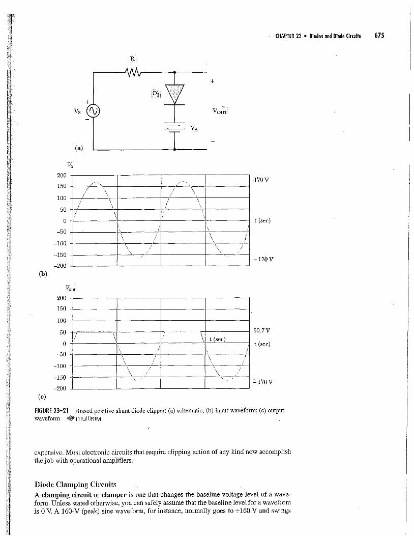
In Figure 23-21, the circuit is biased at 50 Vdc and the positive peak input voltage is 170 V.You can see that the positive limiter is a +50.7-V clipper. Everything above that bias level isclipped off. The negative half of the input waveform is passed to the output without change.
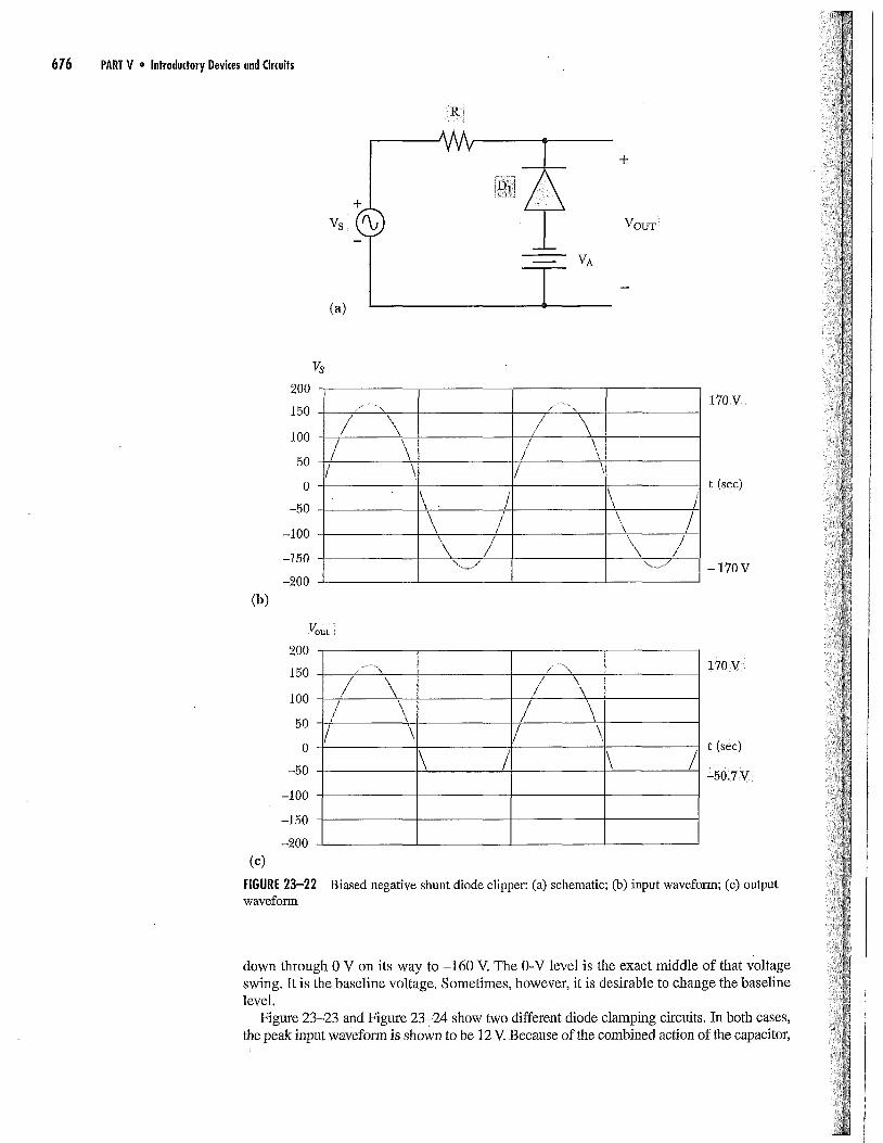
In Figure 23-22, the circuit is biased at-50 Vdc. The clipping action is of the opposite po-Iarity. Here, the negative swing is clipped at-50.7 V, and the positive half-cycle is unchanged.
The de source that is used for setting the bias level for these clipper circuits can be a bat-tery, but you will find that a zener diode (which you will study very soon) is simpler and less
CHAPTER 23 . Diodes and Diode Circuits 675
Vs
+
VOUT
(a)
mVA
T
(b)
200
150
100
50
0-50
-100
-150
-200
Vs
// \/ "\/ \
//
J \1
\
li(//
,/
\\
\\\ //
t70V
t (sec)
- 170V
(c)
Vout
200
150
100
50 /
0-50
-100
-150
-200
\,, /\ ,/% /
//
t (sec)
I,\
\
50.7 V
t (sec)////
//
- 170V
FIGURE 23-21 Biased positive shunt diode clipper: (a) schematic; (b) input waveform; (c) outputwaveform 4ÿmuItisiM
expensive. Most electronic circuits that require clipping action of any kind now accomplishthe job with operational amplifiers.
Diode Clamping CircuitsA damping circuit or damper is one that changes the baseline voltage level of a wave-form. Unless stated otherwise, you can safely assume that the baseline level for a waveformis 0 V. A 160-V (peak) sine waveform, for instance, normally goes to +160 V and swings
676 PART V * Introductory Devices and Circuits
+
Ca)
+
i
!DI!
VOUT
(b)
Vs
200
150
100
50
0
-50
-100
-150
-200
/ \I \
\. /\ /\ /
",.t/
/ \// \
/ \
\ /\ t\ /
170 V
t (s¢ÿ)
- 170V
(c)FIGURE 23-22waveform
50
0-50
-100
-150
-200
150
100
gout
200/ '\
/ '\/ \/ \
\
/ \
/ \/ \/ \/
170 V
t (sÿc)/-50.7 V
Biased negative shunt diode clipper: (a) schematic; (b) input wavefolxa; (c) output
down through 0 V on its way to -160 V. The 0-V level is the exact middle of that voltageswing. It is the baseline voltage. Sometimes, however, it is desirable to change the baselinelevel.
Figure 23-23 and Figure 23-24 show two different diode damping circuits. In both cases,the peak input waveform is shown to be 12 V. Because of the combined action of the capacitor,

CHAPTER 23 . Diodes and Diode Circuits 677
+
+
b gOUT
(a)
Vs
15
10
5
0
-5
-10
-15
"\
/ \ / \\
//
t (sec)
(b)
(c)
FIGURE 23-23waveform
gout
25
20
15
10
5
0
-5
-10
-15
/ \,\, /i
/ \\ /\, /
19.3V
t (sec)
-0.7V
Positive diode clamping circuit: (a) schematic; (b) input waveform; (c) output'ÿ'multiSIM
resistor, and diode, the baseline of the output is radically shifted--positive in Figure 23-23 andnegative in Figure 23-24.
The output voltage levels of these diode clamping circuits depend on the values of C1 andR1, and the frequency of the input waveform. We will not be calculating those values in thischapter, but you should be able to recognize this kind of circuit when you see it on aschematic diagram.

678 PART V ° Introductory Devices and Circuits
+
;C1!
I(
D11 7 R1 VOUT
(a)
Vs
15
10
5J
0
-5
/, +>\/ \
/
-15
(b)Vout
15
10
5
0
-5
-10
-15
-20
-25
(c)FIGURE 23-24waveform
-10
\ //
/ \,' \
/ \/"/ \
\
//f/
t (sec)
// ÿx"N //
/ / "\
ff
\\ /'/
\ /
0.7V
t (sÿc)
- 19.3V
Negative diode clamping circuits: (a) schematic; (b) input waveform; (c) output

CHAPTER 23 * Diodes and Diode Circuits 679
[] IN-PROCESS LEARNING CHECK 2
Fill in the blanks as appropriate.
1. Rectifier diodes are used where it is necessary to change __ current power to __current power.
2. Where additional cooling is necessary, a rectifier diode can be connected to a(n) __to dissipate heat more efficiently.
3. When an ac waveform is applied to a rectifier diode, the diode's rating must begreater than the peak voltage level.
4, The main current specification for rectifier diodes is __
5. To test the forward conduction of a diode with an ohmmeter, connect the __ lead ofthe meter to the cathode and the lead to the anode.
6. The forward resistance of a good diode should be much __ than its reverse resistance.
7. Switching diodes have a(n) __ rating that is hundreds of times less than most rectifierdiodes.
8. The type of diode circuit that removes the peaks from an input waveform is called a(n)circuit.
9. The type of diode circuit that changes the baseline level of an input waveform is called a(n)circuit.
[]
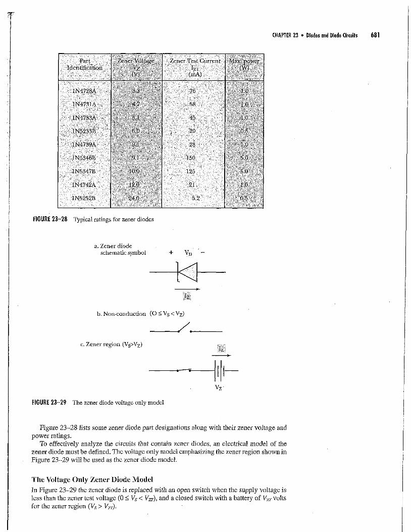
23-6 Zener Diodes
You have already learned that every diode has a certain reverse breakdown voltage specifi-cation. For rectifier and switching diodes, it is essential to avoid circuit conditions that ap-proach their reverse breakdown ratings. The zener diode is different. It is a diode that isdesigned to operate normally in its reverse-breakdown mode.
The zener diode operation is evaluated by using the Figure 23-25 circuit. Figure 23-26shows the LV curve for a zener diode. It is important that you notice the part of the curve thatrepresents the reverse-breakdown current. Once the breakdown voltage is reached, the zenerwill conduct current. In other diodes, this "reverse breakdown" would cause the diode to fail(open). The zener is specially constructed to permit current flow at the reverse breakdown volt-age. Once the PIV rating is reached, the zener diode conducts, allowing current to flow throughthe balance of the circuit (similar to a forward biased diode). The unique action of the zenerdiode causes its REVERSE DROP to stay at this breakdown voltage value. Should the voltageapplied to the zener circuit exceed this voltage (called the "zener" voltage, labeled Vz), all ex-cess voltage will be passed on to the balance of the circuit. This is similar to the 0.7-V drop seenin the forward biased diode (all else is passed on to the circuit).
Zener diodes are available with a wide variety of zener voltages ranging typically from 3 Vto 400 V. The zener diode is often used as a voltage regulator. A voltage regulator is a circuit ordevice that will maintain a constant voltage output given varying voltage input. For example,the voltage produced from the alternator in your car varies its output voltage between 14 V and18 V with engine speed. Zener diodes are used to stabilize this voltage at about 12V. Thus theheadlights don't get brighter and dimmer as the car speeds up and slows down.
The diagram in Figure 23-27 is a simple demonstration circuit. Notice that the symbolfor a zener diode looks like an ordinary diode, but with the cathode-marker bar being benton the ends. Manufacturers specify the zener diode based on the zener voltage (Vz) at thezener test current (IzT) using positive values. Another critical rating for zener diodes is theirmaximum power dissipation. It is very important that the power dissipation of an operatingzener diode does not exceed its power rating. The actual power dissipation of a zener diodeis found using Formula 23-3 by multiplying the voltage dropped across the zener diode bythe current flowing through it.
Ph'acticaH Notes
FORMULA 23-3 P = Iz x Vz
Zener diodes look exactlylike rectifier diodes, astripe near one end marksthe cathode terminal, andthe JEDEC registered zenerdiodes have partdesignations that beginwith 1N. This means thatyou cannot distinguishbetween a standard diodeand a zener diode withoutchecking the specificationsin a data book, catalog, oronline resource (such aswww.FreeTradeZone.com).

680 PART V , Introductory Devices and Circuits
+ +
-1Zener diode test circuit-, FIGURE 23-25
Vs -=-
tÿJ
-VzT
if/
JForwardbias
VD
FIGURE 23-26 Zener diode characteristic curve
1Vsÿ
T
+ ½ -
R
1 +
Vz gOUT
FIGURE 23-27 Zener diode circuit
CHAPTER 23 . Diodes end Diode Circuits 681
PartIdentification
< ÿ"/ÿ ÿ ÿ: ÿi¸°ÿL :¸ /ÿZener Test Current :iMaxliPoWer
IZT (W) :(mA) Ii'ÿ i
1N4728A
1N4731A
1N4733A
1N5233B
1N4739A
1N5346B
76
58
45
2O
28
150
1N5347B
1N4742A
1N5252B ÿ410'
125
21
5.2
1 5.0 ;: :
;: :i:0 ;ÿ:l
FIGURE 23-28 Typical ratings for zener diodes
a. Zener diodeschematic symbol +
b. Non-conduction (O < Vs < Vz)
,/.
c. Zener region (Vs>Vz)
Vz
FIGURE 23-29 The zener diode voltage only model
Figure 23-28 lists some zener diode part designations along with their zener voltage andpower ratings.
To effectively analyze the circuits that contain zener diodes, an electrical model of thezener diode must be defined. The voltage only model emphasizing the zener region shown inFigure 23-29 will be used as the zener diode model.
The Voltage Only Zener Diode ModelIn Figure 23-29 the zener diode is replaced with an open switch when the supply voltage isless than the zener test voltage (0 < Vs < Vzr), and a closed switch with a battery of Vzr voltsfor the zener region (Vs > Vzr).
682 PART V • Introductory Devices and Circuits
The mathematical equation for this model is:
Nonconduction 0 <_ Vs < Vzr Volts
Zener region Vs > Vzr Volts
gz= gsIz=OAVz=VzrIz>0A
You will now analyze the circuit shown in Figure 23-27.
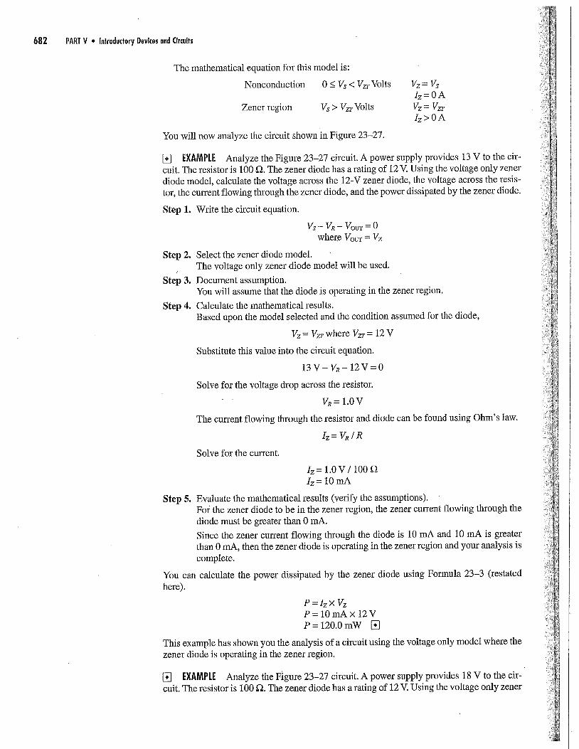
[] EXAMPLE Analyze the Figure 23-27 circuit. A power supply provides 13 V to the cir-cuit. The resistor is 100 ÿ2. The zener diode has a rating of 12 V. Using the voltage only zenerdiode model, calculate the voltage across the 12-V zener diode, the voltage across the resis-tor, the current flowing through the zener diode, and the power dissipated by the zener diode.
Step 1. Write the circuit equation.
VS - VR - VouT = 0where Votrr = Vz
Step 2. Select the zener diode model.The voltage only zener diode model will be used.
Step 3. Document assumption.You will assume that the diode is operating in the zener region.
Step 4. Calculate the mathematical results.Based upon the model selected and the condition assumed for the diode,
Vz = Vzr where Vzr = 12 V
Substitute this value into the circuit equation.
13V- VR- 12V=0
Solve for the voltage drop across the resistor.
" VR= 1.0V
The current flowing through the resistor and diode can be found using Ohm's law.
Iÿ= VR / R
Solve for the current.
Iz= 1.OV/100 gÿIz= 10 mA
Step 5. Evaluate the mathematical results (verify the assumptions).For the zener diode to be in the zener region, the zener current flowing through thediode must be greater than 0 mA.
Since the zener current flowing through the diode is 10 mA and 10 mA is greaterthan 0 mA, then the zener diode is operating in the zener region and your analysis iscomplete.
You can calculate the power dissipated by the zener diode using Formula 23-3 (restatedhere).
P = Iz x YÿP=10mAx 12VP=120.0mW []
This example has shown you the analysis of a circuit using the voltage only model where thezener diode is operating in the zener region.
[] EXAMPLE Analyze the Figure 23-27 circuit. A power supply provides 18 V to the cir-cuit. The resistor is 100 ÿ. The zener diode has a rating of 12 V. Using the voltage only zener

CHAPTER 23 . Diodes and Diode Circuits 683
diode model, calculate the voltage across the 12-V zener diode, the voltage across the resis-tor, the current flowing through the zener diode, and the power dissipated by the zener diode.
Step 1. Write the circuit equation.
gs - VR - VouT = 0where Vour = Vz
Step 2. Select the zener diode model.The voltage only zener diode model wil! be used.
Step 3. Document assumption.You will assume that the diode is operating in the zener region.
Step 4. Calculate the mathematical results.Based upon the model selected and the condition assumed for the diode,
Vz = Vzr where Vzr = 12 V
Solve for the voltage drop across the resistor.
18V- VR- 12V=0gÿ= 6,0V
Solve for the current flowing through the resistor and diode.
Iz= Vÿ/ RIz = 6.0 V / 100 £2Xÿ=60mA
Step 5. Evaluate the mathematical results (verify the assumptions).Since the zener current is 60 mA, then the zener diode is operating in the zener region.
The power dissipated by the zener diode is calculated using Formula 23-3 (restatedhere).
P = Iz X VzP=60mAx 12VP=720.0mW []
From these two examples, you can observe that the output voltage remained at 12 V eventhough the input voltage changed from 13 V to 18 V. The voltage drop across the resistor in-creased, as did the zener current.
Figure 23-30 illustrates a practical voltage regulator circuit. The function of this circuit isto maintain a steady voltage across the load resistor RL while the input voltage varies. When-ever the supply voltage increases, the voltage across the zener diode and the load resistor RLwill remain fixed at the zener diode rated voltage. The voltage drop across the resistor R variesalong with the supply voltage. In addition, the current flowing through the series resistor R andthe zener diode vary accordingly. The load (RL) voltage and current will remain regulated.
FIGURE 23-3D Zener diodevoltage regulator circuit
multisaM

684 PART V * Introductory Devices and Circuits
Whenever the output voltage with the load resistor is less than the zener diode rated voltage,the zener diode is not conducting current and will no longer regulate the voltage for the load.The supply voltage for the regulation transition point can be calculated using Fmanula 23-4. Ifthe supply voltage is less than this voltage, the zener diode is not conducting current and youcan calculate the output voltage by Formula 23-5. If the supply voltage is greater than the reg-ulation transition point supply voltage, the output voltage is regulated by the zener diode ratedvoltage.
FORMULA 23-4 Vs = VZT X (R1 + RL) / RL
FORMULA 23-5 VL = Vs x RL / (RL + R1)
[] EXAMPLE Analyze the Figure 23-30 circuit. The power supply varies from 12 V to 20 V.The load resistor RL is 750 £2 and the resistor Rÿ is 100 £2. The 1N5346B zener diode is used. Cal-culate the regulation transition point supply voltage using Formula 23-4. The zener test voltage rat-ing Vzr for the zener diode 1N5346B is 9.1 V.
Vs = Vzr x (R1 + RD / RLVs=9.1V x (lO0 + 750 £2) / 750 CÿVs = 10.31 V
Calculate the load voltage, load current, and zener current when the supply is 12 V. Sincethe supply voltage is greater than 10.31 V, the voltage that will appear at the load will be lim-ited to 9.1 V since the load resistor is in parallel with the zener diode.
The current flowing through the load resistor is calculated by
IL=VL/RLIL= 9.1V / 750 f)IL = 12.13 mA
To calculate the current flowing through the zener diode, you must calculate the currentflowing through the resistor R1. This current is calculated by
I1 = (Vs - Vz) / R1/1 = (12V- 9.1 V) / 100 £2I1 = 29,0 mA
The current flowing through the zener diode is calculated using Kirchhoff's current law.
Iz=Iÿ -&Iz= 29.0 mA- 12.13 mAIz = 16.87 mA
Now, calculate the load voltage, the load current, and the zener current when the supplyis 20 V.
Since the supply voltage is greater than 10.31 V, the voltage that will appear at the loadwill be limited to 9.1 V.
The current flowing through the load resistor is calculated by
&=VLIRLIL=9.1V/750 ÿIL = 12.13 mA
To calculate the current flowing through the zener diode, you must calculate the currentflowing through the resistor Rÿ. This current is calculated by
11 = (Vs- Vz) /R1Ia = (20V- 9.1V) / 100ÿ1i = 109.0 mA

CHAPTER 23 . Diodes and Diode Circuits 685
The current flowing through the zener diode is calculated using Kirchhoff's current law.
Iz=Xl -ILIz = 109.0 mA - 12.13 mAIz = 96.87 mA []
This example has shown you the analysis of a circuit where the zener diode is used as avoltage regulator. The voltage across the load will drop below the zener rated value of 9.1 Vif the supply voltage is less than 10.31 V. When this occurs the zener diode is no longer con-ducting current and is no longer regulating the load voltage.
PRA(TI(E PROBL[IÿS 3Use the zener circuit in Figure 23-30 where R1 = 1.0 kÿ and Rÿ = 1.0 kÿ with a 1N5233Bzener diode.
1. What is the zener diode voltage rating?
2. Calculate the regulation transition point supply voltage.
3. How much voltage is dropped across the resistor R1 when Vÿ. = 10 Volts?
When Vÿ, = 20 Volts?
4. What is the voltage at Vout when Vj, = 10 Volts?
When Via = 20 Volts?
5. What is the current flowing through RL when Vi, = 10 Volts?
When Vÿn = 20 Volts?
6. What is the current flowing through R1 when Vÿn = 10 Volts?
When Vÿn = 20 Volts?
7. What is the current flowing through the zener diode when Vÿ, --- 10 Volts?
When ¼, = 20 Volts?8. what is the power dissipation of the zener diode when Vÿn = 10 Volts?
When Vÿ, = 20 Volts?
Zener Diode Limiter CircuitsA diode limitcr circuit removes the peaks from an input waveform. Figure 23-31 and Fig-ure 23-32 show examples of shunt limiters using zener diodes. Note that the zener diodesare parallel with this output. In Figure 23-31, the zener diode conducts while the inputwaveform is greater than the zener voltage and less than the zener diode barrier voltage. Inthis circuit the output voltage levels will be limited to between -0.7 V and the zener voltagerating.
The simple shunt limiter in Figure 23-32 is identical with the Figure 23-31 circuit exceptthat the zener diode is reversed in its place across the output. The input waveform is limited,resulting in the output waveform from the negative zener rated voltage to +0.7 V. The addi-tion of a load resistance or the input impedance of another component will change the out-put waveform.
A device similar to the zener diode was developed for high speed, high energy voltage lim-iting. This classification of devices is referred to as transient suppressors. These devices areavailable as unidirectional (dc applications) and bidirectional (ac applications). Transientsuppressors are used to protect electronic equipment from short duration power surges fromlightning strikes. The metal oxide varistor (MOV) has a slower response time but is designedto handle longer duration transient power surges.
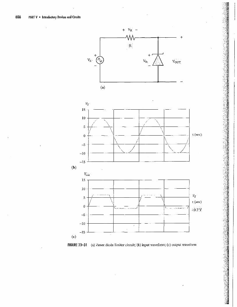
686 PART V • Introductory Devices and Circuits
+VR--
R
VD
+
VOUT
(a)
15
10
5
0
-5
-10
/ \
\ //i\ ........ /
\ /\\ /\ /
t (sec)
-15
(b)Vout
15
o
-5
-10
lO
/ '\ / - \
\ I/ \\ ......... /
Vz
t (sec)
-0.7V
-15
(c)
FIGURE 23-31 (a) Zener diode limiter circuit;(b) input waveform; (c) output waveform

CHAPTER 23 . Diodes and Diode Circuits 687
+
R +
VOUT
(a)
10
5
0
-5
-lO
Ys
15
\ //
//
'\\ ....
t (seÿ)
///
,/
-15
(b)Vout
15
0
-5
-10
10
5
\ /0.7V
t (sec)
-Vz
-15
(c)
FIGURE 23-32 (a) Zener diode limiter circuit; (b) input waveform; (c) output waveform

688
s
PART V * Introductory Devices and Circuits
23-7 Other Types of Diodes
The Tunnel DiodeThe tunnel diode is a two-terminal semiconductor that is manufactured with a high pro-portion of the doping material and an especially thin depletion region. Because of the heavydoping, the ban'ier potential is relatively high, yet because of the thin depletion region, elec-trons can be forced to "tunnel" through the depletion region. At the biasing voltage levels,which cause this tunneling effect, there is a unique feature exhibited by the diode, called thenegative-resistance region of the I-V curve (see Figure 23-33). This means there is a por-tion of the characteristic curve where an increase in forward voltage actually causes a de-crease in forward current.
Negative resistance effects are advantageous in circuits known as oscillators, which youwill learn about later. These oscillator circuits are commonly used to generate high-frequencyac signals. The tunnel diode is also sometimes used as an electronic switch. Its key featurein this application is its high switching speed and low power consumption. Figure 23-34shows the different schematic symbols for tmmel diodes.
The Varactor DiodeVaractor diodes act like small variable capacitors. By changing the amount of reverse biasacross their P-N junction, their capacitance can be varied. The greater the amount of reversebias, the wider the depletion region becomes. Also, the greater the effective distance (deple-tion region) between the P- and N-type sections, the smaller the capacitance is. On the otherhand, the smaller the amount of reverse bias, the nalTower the depletion region and thegreater the amount of capacitance produced. In effect, the varactor is a voltage-variable ca-
Negative resistanceregion
II!
IIII1
V
FIGURE 23-33 1-V curve for a tunnel diode
FIGURE 23-34 Tunnel diode schematic symboIs
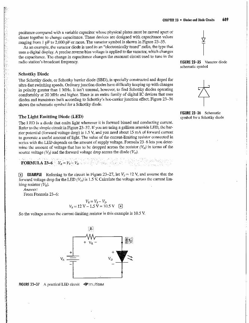
CHAPTER 23 . Diodes and Diode Circuits 689
pacitance compared with a variable capacitor whose physical plates must be moved apart orcloser together to change capacitance. These devices are designed with capacitance valuesranging from I pF to 2,000 pF or more. The varactor symbol is shown in Figure 23-35.
As an example, the varactor diode is used in an "electronically tuned" radio, the type thatuses a digital display. A precise reverse bias voltage is applied to the varactor, which changesthe capacitance. The change in capacitance changes the resonant circuit used to tune in theradio station's broadcast frequency. FIGURE 23-35 Varactor diode
schematic symbol
Sehottky DiodeThe Schottky diode, or Schottky barrier diode (SBD), is specially constructed and doped forultra-fast switching speeds. Ordinary junction diodes have difficulty keeping up with changesin polarity greater than 1 MHz. It isn't unusual, however, to find Schottky diodes operatingcomfortably at 20 MHz and higher. There is an entire family of digital IC devices that usesdiodes and transistors built according to Schottky's hot-carrier junction effect. Figure 23-36shows the schematic symbol for a Schottky diode.
The Light Emitting Diode (LED)The LED is a diode that emits light whenever it is forward biased and conducting current.Refer to the simple circuit in Figure 23-37. If you are using a gallium arsenide LED, the bar-tier potential (forward voltage drop) is 1.5 V, and you need about 15 mA of forward currentto generate a useful amount of light. The value of the current-limiting resistor connected inseries with the LED depends on the amount of supply voltage. Formula 23-6 lets you deter-mine the amount of voltage that has to be dropped across the resistor (VR) in terms of thesource voltage (Vs) and the forward voltage drop across the diode (VD).
FIGURE 23-36 Schematicsymbol for a Schottky diode
FORMULA 23-6 VR = Vs- Vo
[] EXAMPLE Referring to the circuit in Figure 23-27, let Vs = 12 V, and assume that theforward Voltage drop for the LED (VD) is 1.5 V. Calculate the voltage across the current lim-iting resistor (VR).
Answer:From Formula 23-6:
vR= Vs- VvVR =12V-1.5V=10,5V []
So the voltage across the current-limiting resistor in this example is 10.5 V.
R,
gs
+r..
FIGURE 23-37 A practical LED circuit ÿmultisIM

690 PART V ° Introductory Devices and Circuits
Summory• The P-N junction creates a diode. (The prefix "di" indi-
cates two parts.) By applying an external bias voltage to thediode, it can be made to conduct or not to conduct. Con-duction is caused by forward biasing the diode (i.e., nega-tive voltage connected to the N-type material or cathode,and positive voltage connected to the P-type material or an-ode). When reverse biased, the diode will not conduct andacts as an open switch.
• There is a definite distribution of voltages in a circuit con-sisting of a dc power source, a diode, and a resistor con-nected in series. When the dc power source is polarizedsuch that it forward biases the diode, about 0.7 V (forwardvoltage drop) appears across the diode and the remainderof the source voltage appears across the series resistor. Thecurrent through the forward-biased circuit can be calcu-lated by dividing the resistor value into the source voltageminus the forward drop across the diode. When the powersource is connected so as to reverse bias the diode, there isvirtually no current flow through the circuit; the full sourcevoltage can be found across the diode, and zero voltageacross the resistor.
• The three important diode specifications (or ratings) areforward voltage drop (VF), average forward current (Io),and peak reverse voltage (VR). The forward voltage drop,also known as the barrier potential, is the voltage foundacross the diode when it is forward biased and fully con-ducting. This value is about 0.7 V for silicon diodes. Aver-age forward current is the maximum amount offorward-biased current a diode can carry indefinitely. Op-erating a diode outside these specifications for extendedperiods will eventually destroy it.
• Rectifier diodes are designed for converting ac power to dcpower. They can have relatively high current ratings (e.g.,10 A) and heat sinks are often used to cool the diodeswhere this is required.
• Rectifier and switching diodes can be tested with an ohm-meter. A diode in good working order will show a much
higher resistance when it is reverse biased by the ohmme-ter connection than when it is forward biased. A diode isdefective whenever you find the forward and reverse ohm-meter readings in the same general range.
• Switching diodes usually have lower current and voltageratings than rectifier diodes. However, they have muchfaster reverse recovery times. This means switching diodesrecover much faster from reverse-bias conditions than rec-tifier diodes do.
• Diode clipper circuits (also called limiters) remove all or aportion of one polarity from an input waveform. In a seriesclipper, the diode is connected in series with the output ofthe circuit. In a shunt clipper, the diode is connected in par-alM with the output of the circuit. Biased clippers allowclipping at levels other than zero or the forward voltage rat-ing of the diode. The shape of the waveform is drasticallychanged by clipper action.
• Diode clamping circuits change the baseline of an input acwaveform from zero to some other value. The shape of thewaveform is not changed by clamping action.
• Zener diodes are intentionally used in the reverse-breakdownmode. This action fixes the voltage across the zener diode ata specified level. Zener diodes are used where it is necessaryto obtain a steady (regulated) voltage level despite swings inthe input voltage levels. The two main specifications forzener diodes are their reverse voltage drop (Vz) and theirmaximum continuous power.
• A tunnel diode has a negative-resistance I-V curve thatmakes it useful for generating high-frequency waveforms.
• The varactor diode acts like a small capacitor that is vari-able by means of changing the amount of reverse dc biasapplied to it. The larger the reverse bias voltage, thesmaller the amount of capacitance.
• The Schottky diode is specially constructed for ultra-fastswitching times. It is found in high-frequency circuits anddigital IC devices.
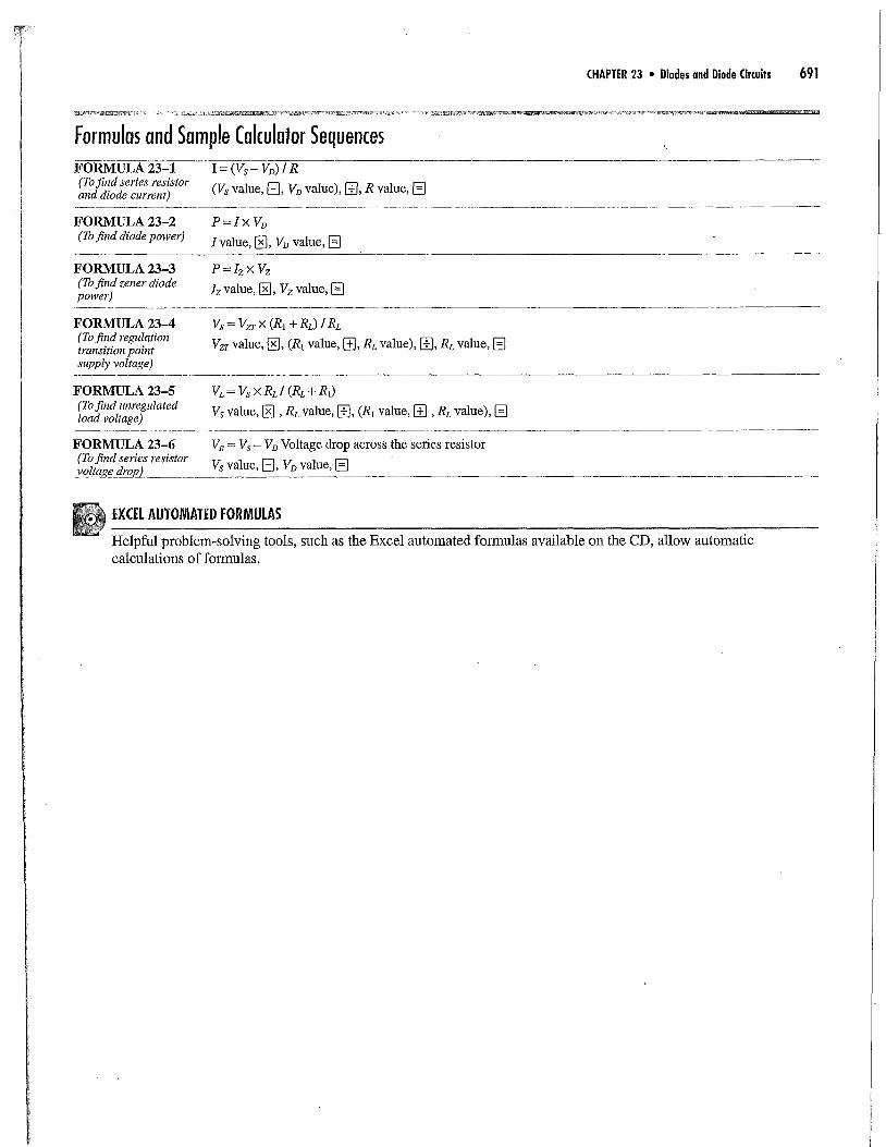
CHAPTER 23 . Diodes and Diode Circuits 691
Formulas and Sample Calculator SequencesFORMULA 23-1(To find series resistorand diode currenO
I= (Vs- VD) / R
(Vs value,/ÿ], Vo value), I-ÿ, R value, []
FORMULA 23-2(To find diode power)
P=IXVD
I value, ['xl, Vo value, []
FORMULA 23-3(To find zener diodepower)
P = Iz X Vz
Iz value, N], Vz value, []
FORMULA 23-4(To find regulationtransition pointsupply voltage)
Vs= Vzr × (R1 + RL) I RL
Vzr value, [], (R1 value, [], RL value), [£], RL value, []
FORMULA 23-5 VL = VS X RL / (RL q- R1)(To find unregulated Vs value, [], RL value, [47, (RI value, [], RL value), []load voltage)
FORMULA 23-6 VR = Vs- VD Voltage drop across the series resistor(To find series resistorvo!tagedrog)_ Vs value, [z], VD value, []
EXCEL AUTOMATED FORMULAS
Helpful problem-solving tools, such as the Excel automated formulas available on the CD, allow automaticcalculations of formulas.

CHAPTER 23 . Diodes and Diode Circuits 693
Review Questions1. Draw two diode circuits, one showing the diode as it is
reverse biased and the second as it is forward biased. La-bel the drawings as appropriate.
2. Indicate the polarity of the voltages dropped across theresistor and diode in Figure 23-38.
3. Modify the circuit in Figure 23-38 by reversing the po-larity of the dc source. Indicate on your drawing the po-larity and amount of voltage across the diode andresistor. Show the amount of current flowing through thecircuit.
4. Sketch the waveform found across the resistor in Fig-ure 23-39. What is the maximum amount of reversevoltage found across the diode?
5. Sketch a circuit for a series diode clipper that clips thepositive levels from the input ac waveform.
6. Sketch a circuit for a shunt diode clipper that clips thenegative levels from the input ac waveform.
7. Describe how a diode clamp circuit affects an ac inputwaveform.
8. Explain the difference between the action of a biaseddiode clipper and a diode clamping circuit.
9. Explain the following diode specifications:
a. Reverse-breakdown voltage
b. Forward conduction voltage
e. Average forward current
d. Reverse recovery time
10. Describe the condition necessary for a zener diode tohold its rated Vz level.
11. Suppose the source voltage in Figure 23-40 increases,What will happen to the voltage across the zener diode?The resistor? How will this increase in applied voltageaffect the current through the circuit?
12. What is the peculiar feature of the I-V curve for tunneldiodes?
13. Draw at least one schematic symbol for a tunnel diode.
14. Name two important applications of tunnel diodes.
15. Describe how a varactor changes capacitance withchanging levels of reverse bias.
16. Describe how Schottk-y diodes are different from mostother kinds of semiconductor diodes.
lu24V ":-
, I, OI330 D. / +
+
12.6 V 5.1 Vÿ
T 1W:
FIGURE 23-38 FIGURE 23-40
o
28 V (rms)
FIGURE 23-39

694 PART V • Introductory Devices and Circuits
Problems1. Referring to the circuit in Figure 23--41, let Vs = 6 V,
Rs = 1 kg2, and VF = 0.7 V. Determine:
a. the total current through the circuit.
b. the voltage drop across resistor Rs.
e. the forward current through the diode.
2. Referring to the circuit in Figure 23-41, let Vs = 12 V andVF = 0.7 V. Determine:
a. the value for Rs that will limit the diode current to500 mA.
b. the power dissipation of Rs.
3. If the maximum current rating for the diode in Figure23-41 is 1 A and Rs = 100 ÿ2, calculate the maximumvalue of Vs that can be applied without exceeding thediode's current rating.
4. Determine the following value for the zener diode circuitin Figure 23-42 where Vs = 20 V, R = 100 ÿ, andD1 = IN4742A:a. voltage drop across the zener diode
b. voltage drop across the resistor
e. current through the circuit
d. the power dissipation of Dr
5. For the circuit in Figure 23-42, let Vs = 12 V,R = 120 ÿ2, and Vz = 9 V. Determine:
a. the voltage across R.
b. the current through the circuit.
e. the power dissipation of R.
d. the power dissipation of Dv
6. Referring to the circuit in Figure 23-42, let Vs = 12 V andVz = 9 V. If the current through the circuit is to be set at1 A, determine:
a. the value of R.
b. the voltage across R.
e. the power dissipation of R.
d. the power dissipation of Dr
FIGURE 23-41
Ol
+
-IFIGURE 23-42
R
D1
o+
7. Suppose the zener diode in Figure 23-42 is rated at6.3 V, the dc power source is 9 V, and the value ofR = 680 ÿ. Determine the amount of power dissipated bythe zener diode.
8. Suppose the dc source voltage in a zener diode circuit(such as in Figure 23-42) increases by 2 V. How muchwill the voltage across the resistor increase? How muchwill the voltage across the zener diode increase?

CHAPTER 23 . Diodes and Diode Circuits 695
Analysis Questions1. Only one of the diodes in the circuit in Figure 23-43 will
conduct. The conducting diode will carry the full currentload, and the other will carry no current. Explain why thishappens. (Hint: There are slight variations in tile forwardconduction voltage.) Explain why connecting a 5-ÿ resis-tor in series with each diode will allow both to conduct,each carrying about half the current load.
2. Use an electronics supply catalog to locate the part num-ber for the rectifier diode that has the highest peak re-verse voltage. Also locate the diode having the highestaverage current rating.
3. Consult an electronics supply website or catalog for thehighest and lowest values for zener diode voltage andpower.
4. Sketch the waveform you might see across the zenerdiode in Figure 23-42 if the zener is rated at 6 V, and thedc voltage source is replaced with an 8-V peak-to-peakac source.
5. Research the basic circuits and range of operating fie-quencies for tunnel diode oscillators.
D1
FIGURE 23-43
6. Use an electronics supply website or catalog to deter-mine the specifications that are important for selectingSchottky diodes.
7. Use a dictionary or glossary of technical terms to de-scribe the difference between discrete and integratedelectronic devices.
MultiSIM Exercise for Resistor-Diode Series Circuits1. Use the MultiSIM program and utilize the circuit shown
in Figure 23-17a.
2. Set the function generator to a 12-V peak sine wave at I kHz.
3. Measure and record the following parameters:
a. Input waveform
b. Output waveform
4. Compare your MultiSIM results with the values given inthe Instructor Guide for this circuit. Were the input andoutput waveforms that you made with MultiSIM reason-ably close to the Figure 23-17b and Figure 23-17cwaveforms ?
Performance Projects Correlation Chart
Chapter Topic Performance Project Project NumberP-N Junction Diodes Forward and Reverse Bias, and I vs. V 61
Diode Clipper Circuits Diode Clipper Circuits 62
Zoner Diodes Zoner Diodes 63
NOTE: It is suggested that after completing the above projects, the student should be required to answer the questions in the "Summary" at the end ofthis section of projects in the Laboratory Manual.