Embed Size (px)
Citation preview
Hannu Sarén
ANALYSIS OF THE VOLTAGE SOURCE INVERTER
WITH SMALL DC-LINK CAPACITOR
Thesis for the degree of Doctor of Science (Technology) to
be presented with due permission for public examination
and criticism in the Auditorium 1383 at Lappeenranta
University of Technology, Lappeenranta, Finland on the
25th of November, 2005, at noon.
Acta Universitatis
Lappeenrantaensis
223
LAPPEENRANTA
UNIVERSITY OF TECHNOLOGY

Supervisor Professor Olli Pyrhönen
Department of Electrical Engineering
Lappeenranta University of Technology
Finland
Reviewers Professor Hans-Peter Nee
Royal Institute of Technology
Sweden
Professor Roy Nilsen
Norwegian University of Science and Technology
Norway
Opponents Professor Roy Nilsen
Norwegian University of Science and Technology
Norway
Professor Heikki Tuusa
Tampere University of Technology
Finland
ISBN 952-214-118-6
ISBN 952-214-119-4 (PDF)
ISSN 1456-4491
Lappeenrannan teknillinen yliopisto
Digipaino 2005

ABSTRACT
Hannu Sarén
Analysis of the voltage source inverter with small DC-link capacitor
Lappeenranta 2005
143 p.
Acta Universitatis Lappeenrantaensis 223
Diss. Lappeenranta University of Technology
ISBN 952-214-118-6, ISBN 952-214-119-4 (PDF), ISSN 1456-4491
In electric drives, frequency converters are used to generate for the electric motor the AC voltage
with variable frequency and amplitude. When considering the annual sale of drives in values of
money and units sold, the use of low-performance drives appears to be in predominant. These
drives have to be very cost effective to manufacture and use, while they are also expected to fulfill
the harmonic distortion standards. One of the objectives has also been to extend the lifetime of the
frequency converter.
In a traditional frequency converter, a relatively large electrolytic DC-link capacitor is used.
Electrolytic capacitors are large, heavy and rather expensive components. In many cases, the
lifetime of the electrolytic capacitor is the main factor limiting the lifetime of the frequency
converter. To overcome the problem, the electrolytic capacitor is replaced with a metallized
polypropylene film capacitor (MPPF). The MPPF has improved properties when compared to the
electrolytic capacitor.
By replacing the electrolytic capacitor with a film capacitor the energy storage of the DC-link will
be decreased. Thus, the instantaneous power supplied to the motor correlates with the
instantaneous power taken from the network. This yields a continuous DC-link current fed by the
diode rectifier bridge. As a consequence, the line current harmonics clearly decrease. Because of
the decreased energy storage, the DC-link voltage fluctuates. This sets additional conditions to the

controllers of the frequency converter to compensate the fluctuation from the supplied motor
phase voltages.
In this work three-phase and single-phase frequency converters with small DC-link capacitor are
analyzed. The evaluation is obtained with simulations and laboratory measurements.
Keywords: frequency converter, voltage source inverter, electrolytic capacitor, film capacitor,
pulse width modulation, overmodulation, space vector modulation, differential space vector
modulation
UDC 621.314.2

ACKNOWLEDGEMENTS
The research work of this thesis has been carried out during the years 2001-2005 at the
Department of Electrical Engineering of Lappeenranta University of Technology. During these
years, I have been working at the university as a research engineer and as a post graduate student
of the Graduate School of Electrical Engineering. This study is part of a larger research project
financed by the company Vacon Plc and National Technology Agency of Finland. The support
from Vacon Plc was much more than purely financial. Although financial support is important, it
proved to be even more crucial for the success of the thesis the opportunity that has been offered
for open discussions between me and the other like-minded researchers working at Vacon Plc.
I would like to express my gratitude to my supervisor, Professor Olli Pyrhönen for his valuable
comments, guidance and very much needed encouragements. I would also like to thank Professor
Juha Pyrhönen for maneuvering me at the beginning of my studies into the exciting fields of
electrical engineering.
The research team was the most important motivation to make my working days feel like carnival.
I really hope that at my future working places the atmosphere will be as vivid, positively twisted
and improvising as experienced together with you my colleagues. Thank you fellows.
I am very much grateful to Mrs. Julia Vauterin for her contribution to improve the language of the
manuscript. Also the other personnel of the department are warmly remembered. Especially
secretary Piipa Virkki for acting sometimes as my travel agent in organizing my conference
travels. I did find, every time, back to home in one piece.
The financial support by the Research Foundation of Lappeenranta University of Technology,
Lapland Engineering and Architect Society, Foundation of Ulla Tuominen, Foundation of
Technology, Foundation of Lahja and Lauri Hotinen, Foundation of Jenny and Antti Wihuri is
greatly appreciated.
My wife Satu deserves many thanks for her love and support. Also many apologies are stated as
the sometimes very straight-laced researcher wondering the mystical phenomena of electricity has
not been the best possible listener and comfort giving partner. For my parents, I wish to express
my gratitude for supporting the goals I wanted to achieve in education as well as in life.
Vantaa, 1st of October 2005 Hannu Sarén

CONTENTS
ABSTRACT....................................................................................................................................3 ACKNOWLEDGEMENTS ............................................................................................................5 CONTENTS....................................................................................................................................7 ABBREVIATIONS AND SYMBOLS ...........................................................................................9 1 INTRODUCTION.................................................................................................................15
1.1 Economical aspects of the electric drives ..................................................................15 1.2 Overview of the voltage source inverters...................................................................20
1.2.1 Motor control...............................................................................................21 1.2.2 Modulator ....................................................................................................23
1.3 Voltage source inverter with small DC-link capacitor ...............................................25 1.3.1 Three-phase input........................................................................................27 1.3.2 Single-phase input .......................................................................................31
1.4 Tools for analysis .......................................................................................................32 1.4.1 Space vector presentation............................................................................32 1.4.2 Dynamic DC-link model .............................................................................35 1.4.3 Electric drive simulation tool ......................................................................37 1.4.4 Frequency domain analysis .........................................................................38 1.4.5 Per-unit values.............................................................................................39
1.5 Experimental test setups.............................................................................................40 1.5.1 Three-phase fed voltage source frequency converter ..................................40 1.5.2 Single-phase fed voltage source frequency converter .................................41
1.6 Outline of the thesis ...................................................................................................42 2 THREE-PHASE FED VOLTAGE SOURCE INVERTER ..................................................47
2.1 Principles of the three-phase AC modulation ............................................................47 2.1.1 Space Vector PWM.....................................................................................47 2.1.2 Overmodulation...........................................................................................52 2.1.3 Analytical estimation of the DC-link voltage fluctuation............................56 2.1.4 Verification of the small DC-link capacitor VSI.........................................57
2.2 Improvement of modulation in the small DC-link capacitor VSI ..............................62 2.2.1 Differential SVPWM (DSVPWM)..............................................................62 2.2.2 Overmodulation in the case of the small DC-link capacitor........................70 2.2.3 Proposed modulation strategy .....................................................................86
2.3 Overvoltage protection...............................................................................................88 2.3.1 Traditional overvoltage protection ..............................................................89 2.3.2 Dynamic Power Factor Control (DPFC) for overvoltage protection...........93
2.4 Resonance between line inductor and DC-link capacitor...........................................99 3 SINGLE-PHASE FED VOLTAGE SOURCE INVERTER ...............................................110
3.1 PWM modulation.....................................................................................................111 3.1.1 Flower Power PWM..................................................................................111 3.1.2 SVPWM with estimated DC-link voltage .................................................115
3.2 Electromechanical resonance ...................................................................................120 3.3 Performance measurements .....................................................................................124
4 CONCLUSIONS.................................................................................................................131 4.1 Three-phase fed VSI ................................................................................................131 4.2 Single-phase fed VSI ...............................................................................................132

4.3 The future scope of the research.............................................................................. 134 REFERENCES........................................................................................................................... 135 APPENDIX A, Simulation parameters for three-phase fed VSI ................................................ 140 APPENDIX B, Simulation parameters for single-phase fed VSI............................................... 141 APPENDIX C, The parameters for three-phase fed test setup ................................................... 142 APPENDIX D, The parameters for single-phase fed test setup ................................................. 143

9
ABBREVIATIONS AND SYMBOLS
A, B, C, E system matrixes of the state-space model
a weighting factor
b Fourier series constant, weighting factor
C capacitance
c space vector scaling constant, cosine amplitude in DFT
c0 scaling constant of the zero-sequence component of the pace vector
D duty cycle
d direct component in synchronously rotating dq reference frame
e electro motive force
f function, frequency
Gg resonance peak amplitude gain
h amplitude of a staircase waveform
i current
In nominal RMS-value of the phase current
J inertia
K torsional spring constant
k sample number of the frequency
L inductance
L1, L2, L3 supply grid phases, line phases
m sector index
M motor
M modulation index
N neutral phase
N number of samples
n Fourier series harmonic number
p power, motor pole pair
P steady-state power
q quadrature component in synchronously rotating dq reference frame
R resistance
S power switch control signal
s sine amplitude in DFT, apparent power
sw switching function

10
t time
te electric torque
tl load torque
tsh shaft torque
T time period of the staircase waveform
Ts switching period of the modulator
u voltage
U, V, W output voltage phases
Un nominal RMS-value line-to-line voltage
U RMS-value line voltage
V active voltage vector
Z impedance
x phase variable of the general three-phase system
X set of complex numbers
x real axis component in xy reference frame
x0 zero sequence component
y filter output
y imaginary axis component in xy reference frame
hα hold-angle
ψ flux linkage
ω angular frequency
Ω1 mechanical system resonance frequency
Ω2 mechanical system anti resonance frequency
∆ change, variation
ψ∆ the change of flux linkage
θ angle
φ phase shift between variables

11
Subscripts
AC Alternating Current
act actual
B base value
d direct component in synchronously rotating dq reference frame
C capacitor
CA Constant Amplitude
calc calculated
CV closest vector
c2g current to grid
DC Direct Current
estim estimated
f fundamental component
fil filter
FP Flower Power
grid supply grid, line
gf grid/filter system
i current
i index, harmonic number
in input
initial initial
inv inverter
l load
lim limited quantity
L1, L2, L3 supply grid phases, line phases
m motor
m sector index
max maximum
mean mean value
meas measured variable
mech mechanical
mod modulated
motor motor

12
nom nominal
n Fourier series harmonic number
on on
off off
OM over-modulation
OMI over-modulation I
OMII over-modulation II
pu per-unit
q quadrature component in synchronously rotating dq reference frame
rec rectifier
ref reference value
res resonance
RMS root mean square, RMS
s stator
sh shaft
six-step six-step modulation
sw switching
u voltage
U, V, W output voltage phases
wobble wobble
x real axis component in xy reference frame
y imaginary axis component in xy reference frame
0 initial value, zero-sequence component
∆ difference
Other notations
x space vector
x matrix
x peak value of x *x complex conjugate of space vector
x absolute value
x vector length

13
Acronyms
A/D Analog to Digital
AC Alternating Current
CA Constant Amplitude
DC Direct Current
DFT Discrete Fourier Transform
DPFC Dynamic Power Factor Control
DSVPWM Differential Space Vector Pulse Width Modulation
DTC Direct Torque Control
EMC Electromagnetic Compatibility
EMF Electromotive Force
FFT Fast Fourier Transform
IGBT Insulated Gate Bipolar Transistor
MPPF metallized polypropylene film capacitor
OM over-modulation
OM I over-modulation I
OM II over-modulation II
PID Proportional Integral Derivative
PWM Pulse Width Modulation
RMS Root Mean Square
SVPWM Space Vector Pulse Width Modulation
THD Total Harmonic Distortion
VSI Voltage Source Inverter
TTL Transistor-Transistor Logic

14

15
1 INTRODUCTION
Control of electric power is the main function of modern-day power converters. In most of the
cases, adjustable voltage amplitude and frequency are required. One of the biggest application
groups on which such demands are set are variable speed drives, where the rotor speed is
controlled to match the need of the application. In this work, the variable speed drives are referred
to as electric drives. In electric drives, frequency converters are used to generate the AC voltage
with variable frequency and amplitude to the electric motor. The electric drives can be categorized
by their dynamical output performance into low-performance and high-performance electric
drives. High-performance applications are for example paper machines, elevators, rolling mills
and various servo drives. The common feature of these applications is the fast torque response of
the produced electric torque and the high precision demand of the speed. Low-performance
electric drives are used in applications where inaccuracy in the produced speed is tolerable and
where the dynamic performance is lower. Low-performance electric drive applications are for
example fans and pumps.
1.1 Economical aspects of the electric drives
According to the market analysis made by a company named ARC Advisory Group (1998), the
power ratings of the low-power, up to 200 kW, electric drives can be categorized into three
groups. Micro drives belong to the category less than 4 kW, low-end drives are in the group from
4 kW to 40 kW and the midrange continues up to 200 kW. The micro drives sell in large
quantities usually through the OEM markets. Low-end drives applications are used mainly in fans
and pumps in building automation industry. Midrange drives are often sold through system
integration or directly to the end-user. The ARC Advisory Group has gathered information on
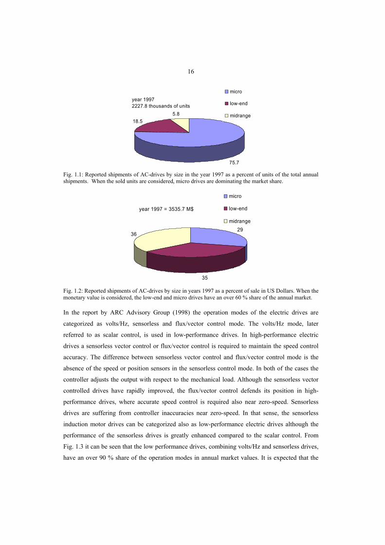
market shares of these power segments from worldwide statistics. Fig. 1.1 shows the reported
units delivered in percent of the corresponding annual unit shipments. The micro drives are
dominating the annual shipments in units. Fig. 1.2 illustrates the reported units delivered in
percent of the corresponding annual sale in million US Dollars. In comparison with the delivered
units in Fig. 1.1 the micro drives are the smallest group in annual sales in US Dollars. No big
changes in monetary percentages are expected.
16
75.7
18.55.8
micro
low-end
midrange
year 19972227.8 thousands of units
Fig. 1.1: Reported shipments of AC-drives by size in the year 1997 as a percent of units of the total annual shipments. When the sold units are considered, micro drives are dominating the market share.
29
35
36
micro
low-end
midrange
year 1997 = 3535.7 M$
Fig. 1.2: Reported shipments of AC-drives by size in years 1997 as a percent of sale in US Dollars. When the monetary value is considered, the low-end and micro drives have an over 60 % share of the annual market.
In the report by ARC Advisory Group (1998) the operation modes of the electric drives are
categorized as volts/Hz, sensorless and flux/vector control mode. The volts/Hz mode, later
referred to as scalar control, is used in low-performance drives. In high-performance electric
drives a sensorless vector control or flux/vector control is required to maintain the speed control
accuracy. The difference between sensorless vector control and flux/vector control mode is the
absence of the speed or position sensors in the sensorless control mode. In both of the cases the
controller adjusts the output with respect to the mechanical load. Although the sensorless vector
controlled drives have rapidly improved, the flux/vector control defends its position in high-
performance drives, where accurate speed control is required also near zero-speed. Sensorless
drives are suffering from controller inaccuracies near zero-speed. In that sense, the sensorless
induction motor drives can be categorized also as low-performance electric drives although the
performance of the sensorless drives is greatly enhanced compared to the scalar control. From
Fig. 1.3 it can be seen that the low performance drives, combining volts/Hz and sensorless drives,
have an over 90 % share of the operation modes in annual market values. It is expected that the

17
share of sensorless vector controlled drives will be greatly increased at the expense of the scalar
control.
80.8
10.98.3
Volts/Hz
Sensorless
Flux/Vector
year 1997 = 3535.7 M$
Fig. 1.3: Reported operation mode of delivered AC-drives in the year 1997 as a percent of costs in US Dollars.
Low dynamic performance does not mean that the electric drive efficiency is not of interest. The
amount of the electric drives is rapidly increasing. Already electric drives are the greatest
electricity consumers in industry and the percentual proportion of the consumed electricity is
increasing. Due to the high volume of the low-performance electric drives in global annual sales
manufacturers have growing interest in low-performance electric drives.
A study by Haataja (2002) gathers information on energy saving potential by using high-
efficiency electric drive technology. Although the efficiency of the motors may be improved, in
many cases improving the efficiency of the mechanical parts of the electric drive has a greater
impact on the total efficiency of the electric drive. As an example of a mechanical part decreasing
the total efficiency of the electric drive, the gearbox may be mentioned.
Almeida (1997) estimates the consumption of electricity in the EU for the end-use in the
industrial and tertiary sector. According to the study, the consumption of electricity can be
divided into following categories: motor, lightning and other. Fig. 1.4 shows the consumption of
electricity shared between these three categories. In industry, Fig. 1.4 a), the motors are the
greatest group with an over 2/3 share. In the tertiary sector, Fig. 1.4 b), the motors are still
representing 1/3 share. When for the motors the consumption of electricity is categorized
according to the applications, the low-dynamic performance drives are found to represent the
majority. Almeida (1997) divides up the share of the electricity consumption by motor drives in
industry and in the tertiary sector according to the different motor applications. This is illustrated
in Fig. 1.5. Although the statistics used are not the most updated, the information received is
clear. It can be seen, that from the total consumption of electricity used by electric drives the share

18
of the low-dynamic performance electric drives varies from 60 % in industry to 80 % in the
tertiary sector. The increase of the electricity used in motor applications per year is 2.2 % in the
tertiary sector and 1.5 % in industry (Hanitsch 2002). In the tertiary sector the smaller motors are
the biggest electricity consumers whereas in industry the consumption is rather equally distributed
between the power ranges. The share of power consumption between the different power ranges is
shown in Table 1.1.
a)69 %
6 %
25 %
MotorLightningOther
EU electricity consumption share for the year 1997 in industry sector 100%=878 TWh
b)
36 %
30 %
34 %
MotorLightningOther
EU electricity consumption share for the year 1997 in tertiary sector. 100%=481 TWh
Fig. 1.4: Estimated electricity consumption in the EU in 1997 for end-use in the a) industrial and b) the tertiary sector.
a)
23 %
16 %
21 %
40 %
PumpsFansCompressorsOthers
Industry
b)
10 %
28 %
42 %
20 %PumpsFansCompressorsOthers
Tertiary
Fig. 1.5: Estimated electricity consumption of motor applications in the EU in 1997 for end-use in the a) industrial and b) tertiary sector.

19
Table 1.1: Estimated electricity consumption in 2010 of the AC motors by power range (Hanitsch 2002).
Power range [kW] Industrial consumption [TWh] Tertiary consumption [TWh]
0.75 – 7.5 148 109
7.5 – 37 136 75
37 – 75 103 25
> 75 258 18
Total 645 227
It can be concluded that the biggest proportion of the electric drives is low-performance drives. It
is also concluded that low-performance drives are the biggest electricity consumer. The total
electricity consumption is most affected by improvements in the category of low-performance
electric drives.
The frequency converter is connected to a supply grid, which in this work is also referred to as a
line. Interactions between the supply grid and the electric drive are of increasing interest. Due to
their working principle power electronic converters cause disturbances in the supply grid. These
disturbances cause the supply grid waveforms to differ from pure sinusoids. Along with the
increasing amount of the electric drives the importance of limiting the disturbances caused by the
electric drive in the supply grid is growing.
There exist different types of standards creating limits for electric device produced harmonic
pollution and disturbances (IEC 61800-3, IEEE-519). These standards are for public electric grids.
In non-public industry grids these standards are not mandatory. However the connection point
between industry and public electric grid do have to meet the standards. Because of the increasing
amount of devices creating electromagnetic disturbance into the grid, there is a growing tendency
to tighten the limits of the standards. The electric drive connected to the supply grid has to pass
the electromagnetic compatibility (EMC) test. To pass the EMC test the device must not create
disturbances higher than allowed by the standards. This is to confirm that the device does not
disturb other devices. The electric device has to be robust against disturbances created by other
devices. This assures that the device remains functional in an environment where electromagnetic
disturbances exist. For the electric drives this means that the line side filtering needs to be taken
into account more carefully. A more complex type of the AC and DC filter needs to be included

20
into the electric drive to fulfill the standards. Another method is to use an active rectifier bridge.
In both cases the electric drive requires a more expensive hardware structure. Vienna rectifier is
one very interesting method to reduce disturbances. In this kind of rectifier three extra switches as
well as a second DC link capacitor are needed compared to the simple diode rectifier. More of the
Vienna rectifier can be found for example from Kretschmar et al. (2001) and Kolar et al. (1994).
For low-performance electric drives the active rectifier bridge is not a cost-effective way to
decrease the line disturbances. This is mainly because of the small demand of regenerative
braking of the pumps and fans. One very comprehensive survey including complex filters and the
active rectifier bridge is done by Pöllänen (2003). Recently, the use of frequency converter driven
low-performance electric drive in home applications has become common. Usually, these kind of
electric drives are single-phase fed systems. For these home appliances to appropriately function,
improvement of the supply grid interactions without the use of expensive active or passive
filtering is required. The dominating feature of electric drives made for home applications is the
cost. Accurate speed control is in these applications usually less important. It can be concluded
that in low-performance drives cost-effective and simple filtering for line side is needed.
The main types of frequency converter topologies are the current source inverter and the voltage
source inverter (VSI). The popularity of the current source inverter is limited by the power
electric configuration. The main drawbacks so far are the lack of proper switching devices, the
bulky DC inductor and more complex controller structure. More information on the current source
inverter topology can be found, for example, in Salo (2002). The most common topology is the
voltage source inverter. In this work, voltage source inverter with diode rectifier is chosen to be
the topology of the frequency converter.
1.2 Overview of the voltage source inverters
The main circuit of the voltage source inverter with three-phase motor load is shown in Fig. 1.6.
In this work, the frequency converter refers to the system having a full-wave diode rectifier
bridge, DC-link and inverter bridge. In the frequency converter, the supply grid AC-voltage is
first rectified using a full-wave rectifier diode bridge. After rectifying, the inverter bridge is used
to convert the DC-voltage into AC-voltage with variable frequency and amplitude. When being
used as a rectifier, the active rectifier bridge, which is identical to the inverter bridge, can be used
to enable regenerative operation of the electric drive. An intermediate circuit with DC-link
capacitor is used to provide energy storage and to filter the DC-link voltage from the rectifier
bridge and inverter bridge voltage spikes. Controlling of the voltage amplitude and frequency is
done by using semiconductor switches, which are turned on and off at high frequency. The motor

21
control algorithms determine the reference to the motor variables. The modulator is used to
convert the reference signal into instances for the six power switches.
gate driver
gate driver
gate driver
gate driver
gate driver
gate driver
~3M
1
1
S
S
2
2
S
S
3
3
S
S
ACL
CL3L2L1
WV,U,
Fig. 1.6: Main circuit of the voltage source frequency converter with three-phase input and three-phase motor. The line phases L1, L2 and L3 are connected to the full-wave diode rectifier bridge. The rectifier transforms AC-voltage into DC-voltage. The DC-link capacitor C, located in the intermediate circuit, is used to smooth the DC-voltage. The inverter bridge is used to transform the DC-voltage into three-phase (U, V, W) AC-voltage with variable amplitude and frequency. The inverter bridge is controlled with the switch commands S1, S2 and S3.
1.2.1 Motor control
There exist different types of motor control algorithms. Field-oriented vector control method
called current vector control is often applied to high-performance electric drives. The current
vector control is well known and discussed in detail, for example, in Kazmierkowski et al. (2002)
and Bose (1997). An alternative method for field oriented control is the direct torque control
(DTC). The DTC was developed almost simultaneously by Depenbrock (1985) and Takahashi et
al. (1986). The method was further developed by Tiitinen et al. (1995). As for the vector
controlled drives, the current trend is to reduce the number of the external measurements as, for
example, motor speed sensors.
The scalar control method is widely applied to low-performance electric drives. The scalar control
adjusts the motor speed by varying the frequency converter output voltage amplitude and
frequency. The induction motor speed is then defined by the loading conditions. Using a speed
feedback, the speed accuracy can be improved. A system equipped with speed feedback is called
closed-loop scalar control. In the scalar control the motor angular frequency is used to form the
amplitude and frequency for the frequency converter output phase voltages. The general form for
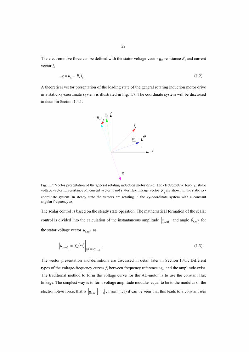
the variable frequency AC-motor drives electromotive force (EMF) vector e in steady state is
defined with the stator flux linkage vector s
ψ and its angular frequency ω
sj ψω−=e . (1.1)
22
The electromotive force can be defined with the stator voltage vector us, resistance Rs and current
vector is
sss iRue −=− . (1.2)
A theoretical vector presentation of the loading state of the general rotating induction motor drive
in a static xy-coordinate system is illustrated in Fig. 1.7. The coordinate system will be discussed
in detail in Section 1.4.1.
x
e
ss iR− suy
si
sψ ω
Fig. 1.7: Vector presentation of the general rotating induction motor drive. The electromotive force e, stator voltage vector us, resistance Rs, current vector is and stator flux linkage vector
sψ are shown in the static xy-
coordinate system. In steady state the vectors are rotating in the xy-coordinate system with a constant angular frequency ω.
The scalar control is based on the steady state operation. The mathematical formation of the scalar
control is divided into the calculation of the instantaneous amplitude refs,u and angle refs,θ for
the stator voltage vector refs,u as
( )ref
urefs, ωωω
== fu . (1.3)
The vector presentation and definitions are discussed in detail later in Section 1.4.1. Different
types of the voltage-frequency curves fu between frequency reference ωref and the amplitude exist.
The traditional method to form the voltage curve for the AC-motor is to use the constant flux
linkage. The simplest way is to form voltage amplitude modulus equal to be to the modulus of the
electromotive force, that is eu =refs, . From (1.1) it can be seen that this leads to a constant u/ω
23
relation. Equation (1.2) shows that stator resistance Rs causes a voltage drop. The effect of the
stator resistance can be included to increase the voltage amplitude accuracy. This is called IR-
compensation. From (1.1) and (1.2) it is possible to calculate the stator voltage vector modulus
reference as
sssrefs,refs, iRu += ψω . (1.4)
Also a quadratic flux linkage frequency dependence can be used. The angle for the stator voltage
vector reference θ s,ref is calculated by integrating the frequency reference ωref as shown in
∫ += ref,0s,refrefs, d θωθ t , (1.5)
where the ref,0s,θ is the initial angle of the stator voltage vector. In many cases the zero initial value
can be used.
Thus the output of the scalar control can be written in vector form as
refs,jrefs,refs, e θuu = . (1.6)
1.2.2 Modulator
Holtz (1992) introduced a very good categorization of the different types of modulators. The two
main methods are the feedforward and feedback schemes.
Feedback schemes generate the switching sequences in a closed control loop. The control loop
can be based on the stator currents or stator flux linkage. As an example the current hysteresis
control and direct torque control methods belong to this category.
Feedforward schemes generate the switched three-phase voltage such that the generated
fundamental voltage vector equals the reference vector. The traditional analog pulse width
modulation (PWM) method which is based on the triangular comparison method as well as the
method called space vector pulse width modulation (SVPWM) belongs to this category. The
SVPWM is suitable especially in digital implementation. The SVPWM method is presented, for
example, in Van Der Broeck et al. (1986) and will be discussed in Section 2.1.1.
The inverter bridge has discrete circuit modes for each set of the switch states. To create a voltage
vector with an arbitrary direction and length, the time averaging approach is used in the
modulation. The modulator is a control circuit that converts the phase reference, or analogously
the voltage vector reference, into switching commands to be fed to the power switches of the

24
inverter bridge. The modulator does not restrict the applied motor control method. In the widely
used Pulse Width Modulation (PWM) method the inverter fundamental output voltage waveform
equals the reference value. The scalar control and modulator block diagram are shown in Fig. 1.8.
refs,u
refω
refω
modulator
scalar control
refω
3
2
1
SSS
refs,jrefs,refs, e θuu = refs,u
∫= tdrefrefs, ωθ
Fig. 1.8: Scalar control and modulator block diagram. The angular frequency reference is fed to the scalar controller. The scalar control transfers the angular frequency reference further to a reference stator voltage vector. The modulator is used to convert the voltage vector into switching commands for the inverter bridge.
When the sinusoidal output fundamental waveform is maintained, the modulation region is called
a linear modulation region. If distortion in the output quantities is tolerable, overmodulation (OM)
methods can be used to increase the output voltage. The behavior of the frequency converter
greatly depends on the modulator type. Especially the overmodulation properties are dependent on
the modulation method. Traditionally, the electric drive voltage output is designed to have its
nominal value noms,u when the nominal angular speed of the motor nomω is used. Overmodulation
methods are used after this point to increase the stator voltage all the way to the maximum limit of
us,max when extra power is needed. This is illustrated in Fig. 1.9.
refs,u
refωnomω
noms,
maxs,
uu
44 344 21
modulationlinear
modulation-over
Fig. 1.9: Principle of the output voltage under linear and overmodulation region as a function of the angular rotating frequency. When the sinusoidal output quantities are maintained, the modulation region is named linear modulation region. Overmodulation can be used to increase the output voltage at the expense of additional distortion in output voltage.

25
1.3 Voltage source inverter with small DC-link capacitor
In the traditional frequency converter, shown in Fig. 1.6, a relatively large electrolytic DC-link
capacitor is used. Many disadvantages are related to the use of this component. Electrolytic
capacitors are large, heavy and rather expensive components. In many cases, the life-time of the
electrolytic capacitor is the main factor limiting the life-time of the frequency converter (Military
Handbook 217 F, Imam et al. (2005)). To overcome the problem, the electrolytic capacitor is
removed. In practice, a small capacitor in the DC-link is necessary to by-bass switching
harmonics of the inverter bridge. This capacitor, however, can be comparably small in
capacitance, if it has sufficient RMS-current capability. Since the metallized polypropylene film
capacitor (MPPF) does not have the same limitations as the electrolytic capacitor and because the
capacitance of the MPPF is approximately one percent of the same volume electrolytic capacitor,
the MPPF is applicable and here chosen to be used as DC-link capacitor. In this work small
capacitor refers to a film capacitor. Technical details and comparison of different capacitor
structures is done e.g. by El-Hussein et al. (2001), Bramoullé (1998) and Michalczyk et al.
(2003). The driving force for this work is to replace the electrolytic capacitor, which works as the
DC-link energy storage, by the MPPF capacitor. Although the changes required for the power
electric hardware configuration remain rather small, the changes have a significant impact on the
frequency converter dynamics and motor control algorithms. By changing the DC-link
capacitance, the dynamic behavior of the DC-link voltage in the frequency converter changes
dramatically. Also the line current harmonic content is improved.
Though replacing the electrolytic capacitor by an MPPF capacitor is a very attractive idea, not
many publications dealing with the small DC-link capacitor frequency converters have been
found by the author. The SED2, which is a product of the company SIEMENS, uses a small DC-
link capacitor. One of the earliest papers on small DC-link capacitor drives was published by
Takahashi et al. (1990). This paper reports the study of a small DC-link capacitor drive equipped
with an active and a passive rectifier bridge. The compensation of the DC-link fluctuation is
implemented in triangle-comparison analog PWM controllers. Bose et al. (1991) eliminates the
DC-link electrolytic capacitor by introducing an active current-fed type high frequency filter in
the DC-link. Minari et al. (1993) studied the frequency converter without DC-link capacitor.
However, the authors used an AC-filter to smooth the rectifier and harmonic components caused
by the inverter bridge. After the study by Minari et al. a few papers dealing with the minimization
of the DC-link capacitor have been published (Kim et al 1993, Alaküla et al. 1994, Wen-Song et
al. 1998, Jung et al. 1999, Namho et al. 2001 and Gu et al. 2002). The motivation for these studies

26
was to match the instantaneous input and output power with each other, thus attaining that no
current flows through the DC-link capacitor. As a consequence, the DC-link capacitor may be
minimized. In these papers mentioned above, an active rectifier bridge is required. Gu et al.
(2005) presented the analytical form to find the minimum capacitance for a frequency converter
having an active rectifier bridge. The matrix converter topology approach is used by Siyoung et
al. (1998). However, the converter configuration presented by the authors is returned to the small
DC-link capacitor VSI with the active rectifier bridge and an additional supply grid filter
component. Kim et al. (1995) use the active rectifier bridge VSI with resonant DC-link without
the electrolytic capacitor. The drawback of the method is that additional power electronic
components are demanded for creating the resonant circuit into the DC-link. Klumpner et al.
(2004) discuss the stability of the VSI equipped with an active rectifier bridge and the problems of
the unbalanced supply grid voltages for small DC-link storage. Two studies on frequency
converter with low-capacitance DC-link capacitor and active rectifier bridge with 120 degree
leading angle have lately been published by Göpfrich et al. (2003) and by Piepenbreier et al.
(2004). The emphasis in Piepenbreier’s et al. (2004) study is placed on the measuring of the
efficiency of the small DC-link capacitor electric drive. Although the study deals with the
frequency converter unit capable of operating in regenerative operation mode, the study can also
be generalized to the motor drive system considered in this work. According to the results
obtained, no considerable change in the efficiency between the small DC-link capacitor drive and
the high-capacitance frequency converter electric drive can be found. Kretschmar et al. (1998)
studied the DC-link fluctuation with simulations and analytic equations for permanent magnet
synchronous motor driven by a frequency converter with small DC-link capacitor.
In this work, only the passive full-wave diode rectifier bridge is considered. The choice is
justified with the small demand of regenerative braking of low-performance drives. No complex
AC-filters are used. Takahashi et al. (1990) considered the same frequency converter structure as
introduced in this work. Contrary to Takahashi’s study, in this work a modern digital control
platform including modulation has been used. New digital modulation methods utilize the DC-
link voltage much more efficiently. This is important especially in the overmodulation region.
Improved measurements as well as control hardware capabilities enable faster controlling of the
frequency converter dynamics. In this study, a DC-link capacitor as small as 2 µF is considered
and its applicability to a frequency converter unit with a 10 A nominal current has been tested.
The capacitance value of the capacitor is approximately 1 % of the original capacitor capacitance.
The selected capacitor is thus even smaller than the capacitors used in the references mentioned

27
above. Kreschmar et al. (1998, 2005) have found that 10 µF capacitor is sufficient for 15 kW
permanent magnet integral motor. This capacitor size leads approximately to same ratio of
capacitance and electric drive power as in this research.
The above literature survey covers the three-phase fed VSI and does not take into consideration
the single-phase supplied VSI. Only a few scientific studies dealing with the single-phase
supplied small DC-link VSI have been published. Publications as by Takahashi et al. (2001,
2002), Haga et al. (2003) and Lamsahel et al. (2005) consider the single-phase fed small DC-link
capacitor VSI with permanent magnet motor. The papers differ from each other by the applied
motor control algorithms. One patent EP1396927 by Takahashi et al. (2004) has been registered.
The power electronic configuration used in this patent is exactly the same as that used in this
work. However, in this work different motor control algorithms are used. Lately, a study by the
author (Sarén et al. 2005) presents the single-phase fed VSI with a small DC-link capacitor and
DTC control for a three-phase induction motor. The fact that only few references for the single-
phase fed small DC-link capacitor VSI were found by the author indicates that no extensive
research and publications on this subject have yet been done.
1.3.1 Three-phase input
Replacing the electrolytic capacitor by a smaller MPPF capacitor will dramatically decrease the
energy stored in DC-link. When a symmetrical load and sinusoidal output voltages and currents
are assumed the three-phase instantaneous output power is constant at every instant. The three-
phase full-wave diode rectifier bridge is capable of supplying a continuous power which is equal
to the instantaneous output power. Thus, it is not necessary to have energy storage in DC-link in
the case of a symmetrical three-phase system. The figures below illustrate the change in the DC-
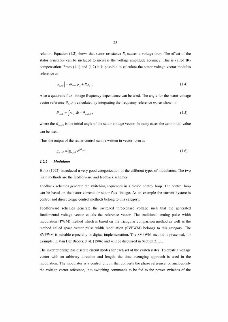
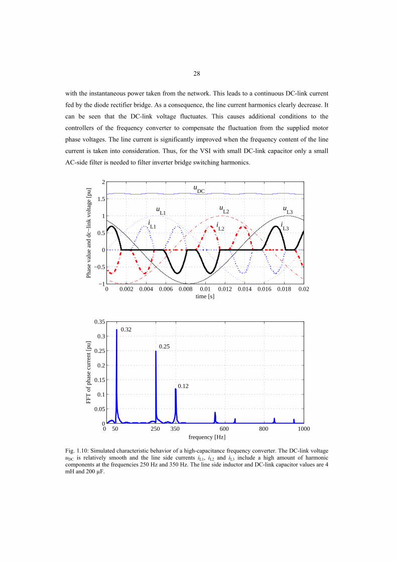
link voltage and the line currents comparing the high-capacitance frequency converter with the
frequency converter with small DC-link capacitor. The inductor used as an AC-filter and the DC-
link capacitor are scaled 10 % and 1 % from the original values being 4 mH and 200 µF
respectively. In both cases, the simulated DC-link voltage, the supply grid phase voltages and
currents are shown. And in both cases constant, equal power is taken from the DC-link. Fig. 1.10
shows the characteristic behavior of a high-capacitance three-phase frequency converter. The DC-
link voltage uDC is relatively stable and the line side currents iL1, iL2 and iL3 include a high amount
of harmonic current components at the frequencies 250 Hz and 350 Hz, causing problems to the
supply grid. The corresponding behavior of a frequency converter with small DC-link capacitor is
shown in Fig. 1.11. Replacing the electrolytic capacitor by a film capacitor will decrease the
energy storage of the DC-link. Thus, the instantaneous power supplied into the motor correlates
28
with the instantaneous power taken from the network. This leads to a continuous DC-link current
fed by the diode rectifier bridge. As a consequence, the line current harmonics clearly decrease. It
can be seen that the DC-link voltage fluctuates. This causes additional conditions to the
controllers of the frequency converter to compensate the fluctuation from the supplied motor
phase voltages. The line current is significantly improved when the frequency content of the line
current is taken into consideration. Thus, for the VSI with small DC-link capacitor only a small
AC-side filter is needed to filter inverter bridge switching harmonics.
0 0.002 0.004 0.006 0.008 0.01 0.012 0.014 0.016 0.018 0.02−1
−0.5
0
0.5
1
1.5
2
time [s]
Phas
e va
lue
and
dc−
link
volta
ge [
pu]
0 50 250 350 600 800 10000
0.05
0.1
0.15
0.2
0.25
0.3
0.35
frequency [Hz]
FFT
of
phas
e cu
rren
t [pu
]
uL1
iL1
uL2
iL2
uL3
iL3
0.32
0.25
0.12
uDC
Fig. 1.10: Simulated characteristic behavior of a high-capacitance frequency converter. The DC-link voltage uDC is relatively smooth and the line side currents iL1, iL2 and iL3 include a high amount of harmonic components at the frequencies 250 Hz and 350 Hz. The line side inductor and DC-link capacitor values are 4 mH and 200 µF.
29
0 0.005 0.01 0.015 0.02−1
−0.5
0
0.5
1
1.5
2
time [s]
Phas
e va
lue
and
dc−
link
volta
ge [
pu]
0 50 250 350 600 800 10000
0.05
0.1
0.15
0.2
0.25
0.3
0.35
frequency [Hz]
FFT
of
phas
e cu
rren
t [pu
]
uDC
uL1
iL1
uL2
iL2
uL3
iL3
0.32
0.055
0.04
Fig. 1.11: Simulated characteristic behavior of a frequency converter with line side inductor and DC-link capacitor. The values of the line side inductor and DC-link capacitor are scaled 10 % and 1 % from the original ones being 0.4 mH and 2 µF respectively. The DC-link voltage uDC fluctuates. The line current significantly improves when the frequency content of the current is taken into consideration.
The supply grid current waveform in Fig. 1.11 strongly defends the configuration of the small
DC-link capacitor VSI. The line current waveform is a real benefit. Approximating the line
current with a staircase waveform with amplitude h, shown in Fig. 1.12, the current can be written
in terms of the Fourier series
( ) ∑∞
=⎟⎠⎞
⎜⎝⎛=
1
π2sinn
n tT
nbtf , (1.7)

30
where n stands for the harmonic number, T is the period of the staircase waveform and the
constants bn can be calculated from
( )
.π67cosπ
65cosπ
611cosπ
61cos
π
dπ2sin-dπ2sin2
dπ2sin2
/1211
/127
/125
/12
0
⎥⎦
⎤⎢⎣
⎡⎟⎠⎞
⎜⎝⎛−⎟
⎠⎞
⎜⎝⎛−⎟
⎠⎞
⎜⎝⎛+⎟
⎠⎞
⎜⎝⎛=
⎥⎦
⎤⎢⎣
⎡⎟⎟⎠
⎞⎜⎜⎝
⎛⎟⎠⎞
⎜⎝⎛⋅+⎟⎟
⎠
⎞⎜⎜⎝
⎛⎟⎠⎞
⎜⎝⎛⋅=
⎟⎟⎠
⎞⎜⎜⎝
⎛⎟⎠⎞
⎜⎝⎛=
∫∫
∫
nnnnn
h
ttT
nhttT
nhT
ttT
ntfT
b
T
T
T
T
T
n
(1.8)
Now it is possible to approximate the amplitude of the different harmonic components of the
supply grid current waveform shown in Fig. 1.11. The Fourier transform suggests that the
amplitude of the 5th and the 7th harmonic compared to the fundamental component waveform
magnitude are b5/b1 =1/5 and b7/b1=1/7. From Fig. 1.11 it can be seen that this is not exactly the
case. However, the current staircase waveform approximation is reasonably accurate.
−1.5
−1
−0.5
0
0.5
1
1.5
time [s]
Lin
e cu
rren
t am
plitu
de h
f(t) b1sin(2πt/T)
T/12 5T/12 7T/12 11T/12
T=0.02s
T/4 3T/4 T0 T/2
Fig. 1.12: Approximation of a small DC-link capacitor VSI line current waveform with the staircase waveform f(t) with the amplitude h. The fundamental waveform amplitude is b1.
The DC-link voltage fluctuates periodically at a frequency which is 6-fold the supply grid
frequency. In a 50 Hz supply grid the fluctuation frequency is thus 300 Hz. This indicates that the
modulator should take into account the DC-link voltage level. Takahashi et al. (1990) describe an
analog implementation of the PWM modulator that is capable of taking the 300 Hz DC-link

31
fluctuation into account. The main idea proposed in the article is to use the amplitude of the
carrier signal which fluctuates synchronously with the DC-link voltage at a frequency of 6-fold
the supply grid frequency. In the space vector pulse width modulation, the DC-link voltage is
observed in the calculation of the pulse width references.
1.3.2 Single-phase input
In the case of a single-phase input, dramatic changes will be observed in comparison with the
three-phase system. The input power is not constant. The main diagram of the hardware
configuration discussed is shown in Fig. 1.13.
gate driver
gate driver
gate driver
gate driver
gate driver
gate driver
~3M
1
1
S
S
2
2
S
S
3
3
S
S
ACL
CNL1 WV,U,
Fig. 1.13: Main circuit of the voltage source frequency converter with single-phase input and three-phase motor load.
The instantaneous power gained from the sinusoidal one phase system in steady state is
( ) ( ),sinˆsinˆ gridgrid
L1L1in
φωω −⋅=
=
titu
iup (1.9)
where iu ˆandˆ indicate the peak values of the phase voltage and current respectively. The angle φ
is the phase shift between the voltage and current.
If the phases of the line voltage and current are identical, that is 0=φ , the instantaneous power
becomes
( ).sinˆˆ grid2
in tiup ω= (1.10)
This indicates that the output power should also fluctuate in a similar way to gain a purely
sinusoidal line current behavior and unity power factor. This also represents the maximum
possible continuous power supply gained from the single-phase fed small capacitance frequency
converter under sinusoidal line voltage and current. The situation is illustrated in Fig. 1.14. By

32
using the small DC-link capacitor a cost-effective power electronic configuration can be achieved.
This is important especially in the applications of electric drives in home appliances.
0 0.005 0.01 0.015 0.02−1
−0.5
0
0.5
1
1.5
time [s]
u DC
, uL
1 and
i L1 [
pu]
π iL1
uL1
uDC
π /22π
pin
Fig. 1.14: The DC-link voltage uDC, line voltage uL1 and current iL1 and input power pin waveforms with a small DC-link capacitor under resistive load. To gain a purely sinusoidal line current waveform the output power must match the waveform of the theoretical input power waveform.
1.4 Tools for analysis
Next, the most essential mathematical tools used in this work are defined and explained. The
three-phase systems are simplified into a vector presentation by using the space vector
presentation. Simulation is a very important method for verifying the ideas and methods before
implementing them into practice. In this work a considerable number of simulation results are
presented. The frequency domain analysis is used to study the behavior of the electric drive
quantities. Per unit values are used to make comparison between different power scales easier.
1.4.1 Space vector presentation
For the modeling of three-phase systems space vectors are proved to be a very useful means. The
theory was invented by Kovacs and Racz (1959) and it was originally intended for the transient
analysis of AC machines. In a general three-phase system, which has an angular frequency ω , the
instantaneous values of the phase quantities x and phase the angle are expressed as
( ) ( ) ( ) ( )( )tttxtx UUU cosˆ φθ += (1.11)

33
( ) ( ) ( ) ( )⎟⎠⎞
⎜⎝⎛ +−= tttxtx VVV π
32cosˆ φθ (1.12)
( ) ( ) ( ) ( )⎟⎠⎞
⎜⎝⎛ +−= tttxtx WWW π
34cosˆ φθ (1.13)
( ) ( )∫=t
ttt0
dωθ , (1.14)
where x is the phase quantity peak value.
The system can be expressed with a complex space vector and real zero-sequence component ( )tx
and ( )tx0 respectively as
( ) ( ) ( ) ( )
( ) ( )tθtx
txtxtxctx
j
34πj
W3
2πj
VU
e
ee
=
⎥⎥⎦
⎤
⎢⎢⎣
⎡++=
(1.15)
( ) ( ) ( ) ( )[ ]txtxtxctx WVU00 ++= . (1.16)
The underlined variables express the space vector in a stationary reference frame and the angle θ
is the space vector angle from the real axis of the stationary reference frame. The terms c and 0c
are used in the vector scaling. Peak value scaling is achieved when 3/2=c and 3/10 =c are
selected whereas the power invariant form of the space vectors is achieved with the values
3/2=c and 3/10 =c . In this work peak value scaling is used.
The space vector presentation (1.15) can be expressed with a real and an imaginary component
denoted with the subscripts x and y as
( ) ( ) ( )txtxtx yx j+= . (1.17)
The real and imaginary components can be calculated from the following matrix relation as
( )( )( )
( )( )( )⎥
⎥⎥
⎦
⎤
⎢⎢⎢
⎣
⎡
⎥⎥⎥
⎦
⎤
⎢⎢⎢
⎣
⎡−−−
=⎥⎥⎥
⎦
⎤
⎢⎢⎢
⎣
⎡
txtxtx
txtxtx
W
V
U
0
y
x
3/13/13/13/13/10
3/13/13/2, (1.18)
where the x0 is a zero-sequence component.

34
In a symmetric three-phase system the peak values and phase angles of the three-phase system are
equal. The zero-sequence component x0 thus becomes zero and can be omitted in the space vector
analysis. The coordinate systems presented in this work are based on this real/imaginary
coordinates. Later, the coordinates are shortly denoted as xy-coordinates.
The instantaneous value of the phase variables, when peak value scaling is used, can be obtained
from
( ) ( ) ( )
( ) ( ) ( )
( ) ( ) ( )txtxtx
txtxtx
txtxtx
03
4πj-
W
03
2πj-
V
0U
eRe
eRe
Re
+⎪⎭
⎪⎬⎫
⎪⎩
⎪⎨⎧
=
+⎪⎭
⎪⎬⎫
⎪⎩
⎪⎨⎧
=
+=
. (1.19)
The transformation from the xy-components to the three-phase system is defined in the matrix
form as
( )( )( )
( )( )( )⎥
⎥⎥
⎦
⎤
⎢⎢⎢
⎣
⎡
⎥⎥⎥
⎦
⎤
⎢⎢⎢
⎣
⎡
−−−=
⎥⎥⎥
⎦
⎤
⎢⎢⎢
⎣
⎡
txtxtx
txtxtx
0
y
x
W
V
U
12/32/112/32/1101
. (1.20)
The instantaneous power of the three-phase system ( )tp is equal to the sum of each phase
instantaneous power
( ) ( ) ( ) ( ) ( ) ( ) ( )titutitutitutp WWVVUU ++= . (1.21)
The instantaneous power can be expressed with the space vector presentation when the phase
voltages and currents are expressed with equation (1.19) as
( ) ( ) 00yyxx
00*
323
3Re23
iuiuiu
iuiutp
++=
+=. (1.22)
In this work the most often used terms stator voltage and current vectors in the xy-coordinate
system are denoted as us and is. The vectors are defined by using the output phase U, V and W
quantities of the voltage source inverter. The equations are written as

35
( ) ( ) ( ) ( )
( ) ( )
ys,xs,
js
34πj
W3
2πj
VUs
je
ee32
u
uutu
tutututu
t
+=
=
⎥⎥⎦
⎤
⎢⎢⎣
⎡++=
θ (1.23)
and
( ) ( ) ( ) ( )
( ) ( )
.je
ee32
ys,xs,
js
34πj
W3
2πj
VUs
i
iiti
titititi
t
+=
=
⎥⎥⎦
⎤
⎢⎢⎣
⎡++=
θ (1.24)
1.4.2 Dynamic DC-link model
The dynamic model of the DC-link is needed to verify the behavior of the DC-link voltage under
different load conditions and with different electrical parameters. The dynamic model includes a
line side resistance RAC and inductance LAC. The variables are defined without using the time
variable for simplicity. The supply grid voltage vector gridu is defined as
34πj
L33
2πj
L2L1grid ee uuuu ++= . (1.25)
The line current vector gridi on the AC-side can be calculated from
recgridgridACgrid
AC dd
uuiRt
iL −=+ , (1.26)
where urec is a rectifier voltage.
The functionality of the full-wave rectifier bridge can be modeled with the switching function
recsw . The function is defined as
34πj
L3rec,3
2πj
L2rec,L1rec,rec esweswswsw ++= . (1.27)
If a diode is modeled as an ideal switch the sign of the corresponding line current determines the
on/off state of the diode. The function can be expressed as
( )ii if ,gridrec,sw = , (1.28)
where the subscript 3LandL2,1L=i .

36
The state of irec,sw is defined as
⎪⎩
⎪⎨⎧
≤
>=
0when,0
0when,1sw
,grid
,gridrec,
i
ii i
i. (1.29)
The rectifier current reci is expressed as a function of the switching function swrec and the line
current vector
*gridrecrec swRe
23 ii = . (1.30)
The rectifier voltage vector recu at the AC-side is also defined with the switching function.
DCrecrec sw uu = , (1.31)
where the DC-link voltage DCu depends on the rectifier current reci and the inverter current invi
and is defined as
( )invrecDC 1
dd ii
Ctu
−= , (1.32)
where C is DC-link capacitance.
The approximate model for the DC-link voltage with no commutation and inverter current effect
can be expressed as
( )L1L3L3L2L2L1DC ,,max uuuuuuu −−−= . (1.33)
The circuit diagram of the DC-link dynamic model is shown in Fig. 1.15.
ACAC LR
C
invi
DCu
gridu recu
gridi
L3L2L1
reci
Ci
Fig. 1.15: Main circuit diagram of the dynamic DC-link model. The parameters are the line side resistance and the inductances RAC and LAC respectively and the DC-link capacitance C.

37
1.4.3 Electric drive simulation tool
To verify the functionality of the whole electric drive a simulation model was built. For this work
Matlab® Simulink® by the company MathWorks has been used as a simulation program.
Simulink includes a power circuit simulator which, previously known as PowerSystem
Blockset®, has been lately renamed SimPowerSystem®. The power circuit simulator allows the
user to configure the power circuit diagram as well as the motor model by using ready-made
blocks and simply initializing the electrical parameters of the blocks. All the control algorithms,
including modulators, can be made by using standard Simulink blocks. The modulator using the
PWM method needs a discrete time simulation model with a very short sample time or preferably
a time continuous model. Due to the long simulation durations the main model used is a
discretized simulation model. To preserve for the PWM a sufficient accuracy, sample time steps
from 5 µs to 0.01 µs are used depending on the scope of the simulation case.
Fig. 1.16 shows the used electric drive simulation model in block diagram. The supply grid model
includes the ideal three-phase 50 Hz sinusoidal voltage supply with a peak value of 2230 V. The
line impedance is set to zero. The purely inductive inductor LAC is applied as the AC-filter. A
universal bridge configured as full-wave diode bridge is used as the rectifier. A capacitor C is
used in the intermediate circuit. A universal bridge configured as an IGBT bridge is used as the
inverter bridge. A three-phase asynchronous motor model with external load torque tl capability is
used as the motor model. All these basic blocks are available in the SimPowerSystem® blockset.
References for these blocks are given, for example, on MathWorks’ manual (Simulink, 2000).
The control circuits are built using discrete time blocks to emulate the digital behavior of the
controllers. The scalar control has been described earlier in this work. The modulator equations
will be presented in detail in the next chapter. Blanking time logic is used to make the control
signals of the upper and lower IGBT arm switches with added blanking time between the
switching instants. Blanking time is used to prevent short circuit between the same phase upper
and lower IGBT arm. The parameters used in the simulations are listed in the appendices.
Appendix A includes the parameters related to the three-phase fed simulation model. Appendix B
includes the parameters related to the single-phase fed simulation model.

38
~3 Asynchronous
Machine, pu units
L3L2L1
1
1
S
S
ACL CWV,U,
Universal bridge (IGBT)
Universal bridge (DIODE)
3-phase inductor
6
Scalar Control
Modulator
refs,jrefs,refs, e θuu =
∫= tdrefrefs, ωθ
refs,u
refω
refω refs,u
3
2
1
SSS
lt
3-phase Supply
grid
2
2
S
S
3
3
S
S
Blanking time logic
Fig. 1.16: Basic components of the electric drive simulation model. The ideal sinusoidal three-phase voltage supply is used as the supply grid model. A three-phase parallel inductor is used to describe the line side AC-filter. The universal bridge parameterized as the diode and the IGBT bridge are used to respectively model the full-wave rectifier and IGBT bridge. The three-phase asynchronous motor with pu units is used as the motor model. The load torque is adjustable. A fully working scalar control with modulator is included into the model to gain the IGBT bridge control signals. The blanking time logic is used to prevent short circuit between the DC-link positive and negative bus-bar.
1.4.4 Frequency domain analysis
In many cases, an analysis being capable of analyzing the frequencies that are contained in one
signal offers considerable advantages. The Fourier analysis is used to decompose the signals into
sinusoids. For the sampled signals, the discrete Fourier transform (DFT), also called finite Fourier
transform, is employed. The DFT is widely used in signal processing and in related applications.
The DFT can be quickly computed using a fast Fourier transform (FFT) algorithm. In the DFT
sine and cosine waves are applied. The number of samples, indexed with i in the time domain, is
denoted as N. The time domain having N points corresponds to N points in the frequency domain.
The output of the DFT is a set of complex numbers X that represent the amplitudes of the cosine
and sine waves c and s respectively for each frequency f with index k=fN. The DFT output X is
[ ] [ ] [ ]
[ ] ,e1
jj2π1
0
NikN
iix
N
kskckX−−
=∑=
+= (1.34)

39
where the i is the time domain index and k∈0, 1,…, N-1 stands for the sample number of the
frequency.
The inverse DFT assigns each of the amplitudes to the corresponding cosine and sine waves. The
result is a set of scaled sine and cosine waves that can be added to form the time domain signal. In
general, any N point repetitive signal can be created by adding cosine and sine waves. Adding the
scaled sine and cosine waves produces the time domain signal x[i].
[ ] [ ]
[ ] ( ) ( )( ) [ ] ( ) ( )( ).π2cosjπ2sinπ2sinjπ2cos1
0
1
0
j2π1
0
NkiNkiksNkiNkikc
ekXix
N
k
N
k
NikN
k
−−+=
=
∑∑
∑−
=
−
=
−
= (1.35)
More on the DFT can be found, for example, in Smith (1999). In this work, a ready-made
Matlab® FFT function for studying sampled data in the frequency domain is used. Here, the
frequency domain quantities are denoted shortly as FFT values.
1.4.5 Per-unit values
Per-unit values are used to scale different power scale values into a comparable form. The per-
unit (pu) system is a dimensionless relative value system defined in terms of base values denoted
with subscript B. A per-unit value is defined as
Bpu x
xx = , (1.36)
where x is the absolute physical value of the quantity and xB is its base value.
The fundamental base values are defined as
,π2:frequency
2:current
32:voltage
gridB
nB
nB
f
Ii
Uu
=
=
=
ω
(1.37)
where Un is the nominal root mean square (RMS) value of the converter line-to-line voltage, In is
the nominal RMS-value of the converter phase current and fgrid is the supply grid line voltage
frequency.
40
From the fundamental base values other base values can be derived as follows:
( )
( ) ( )
.323 :power
and :linkageflux
,1 :ecapacitanc
, :inductance
, :resistanceandimpedance
,1:time
nnBBB
BBB
BBBBBB
BBBBBB
BBBB
BB
IUius
u
uiZC
iuZL
iuRZ
t
==
=
==
==
==
=
ωψ
ωω
ωω
ω
(1.38)
1.5 Experimental test setups
The presented ideas and theories can be verified by use of experimental devices. The commercial
frequency converters that belong to the VACON NX™-family are used as power electronic
hardware. With this hardware platform it is possible to feed the external switching commands S1,
S2 and S3. The ASIC integrated in a VACON NX™ frequency converter further converts these
commands for each IGBT power switch with added hardware specific blanking time. The
switching commands are obtained from the dSPACE™ real time control card. All the control
algorithms including the modulator are included in the dSPACE™ real time control card. An
example of dSPACE™ controller usage is given, for example, by Sarén et al. (2002a). For this
study, slightly differing experimental settings for the three-phase and single-phase fed devices
were built. During the research work a considerable number of measurements have been carried
out.
1.5.1 Three-phase fed voltage source frequency converter
A standard 4 kW 3-phase four-pole induction motor is used as the controlled motor. A 5.5 kW
induction motor with regenerative speed controlled VACON CX™ unit is used as the load. The
motors are connected back to back by stiff shaft coupling. In appendix C the essential
experimental setup parameters are listed. The theoretical diagram of the used experimental device
is shown in Fig. 1.17. The original 165 µF electrolytic capacitor is replaced with a 2 µF MPPF
capacitor. As the line filter, a 0.4 mH inductor is used instead of the original 3.4 mH. The phase
current and DC-link voltage measurement cutoff frequency of the analog low pass filter is 100
41
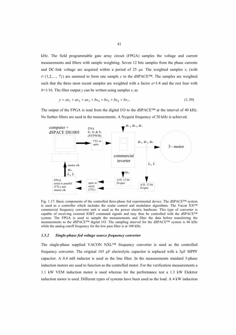
kHz. The field programmable gate array circuit (FPGA) samples the voltage and current
measurements and filters with sample weighting. Seven 12 bits samples from the phase currents
and DC-link voltage are acquired within a period of 25 µs. The weighted samples xi (with
i=1,2,…, 7) are summed to form one sample y to the dSPACE™. The samples are weighted
such that the three most recent samples are weighted with a factor a=1/4 and the rest four with
b=1/16. The filter output y can be written using samples xi as
7654321 bxbxbxbxaxaxaxy ++++++= . (1.39)
The output of the FPGA is read from the digital I/O to the dSPACE™ at the interval of 40 kHz.
No further filters are used in the measurements. A Nyquist frequency of 20 kHz is achieved.
computer + dSPACE DS1005
commercial inverter
3~ motor
uDC
A/D, 12 bitD/optic A/D, 12 bit
D/optic
FPGAserial to parallel (TTL) andmaster clk
optic to serial (TTL)
master clk
ENAS1, S2 & S3
(SVPWM)
TTL to optic
uDC
iU, iV
uL1, uL2, uL3
uU, uV, uW
iU, iV
Fig. 1.17: Basic components of the controlled three-phase fed experimental device. The dSPACE™ system is used as a controller which includes the scalar control and modulator algorithms. The Vacon NX™ commercial frequency converter unit is used as the power electric hardware. This type of converter is capable of receiving external IGBT command signals and may thus be controlled with the dSPACE™ system. The FPGA is used to sample the measurements and filter the data before transferring the measurements to the dSPACE™ digital I/O. The sampling interval for the dSPACE™ system is 40 kHz while the analog cutoff frequency for the low pass filter is at 100 kHz.
1.5.2 Single-phase fed voltage source frequency converter
The single-phase supplied VACON NXL™ frequency converter is used as the controlled
frequency converter. The original 165 µF electrolytic capacitor is replaced with a 3µF MPPF
capacitor. A 0.4 mH inductor is used as the line filter. In the measurements standard 3-phase
induction motors are used to function as the controlled motor. For the verification measurements a
1.1 kW VEM induction motor is used whereas for the performance test a 1.3 kW Elektror
induction motor is used. Different types of systems have been used as the load. A 4 kW induction
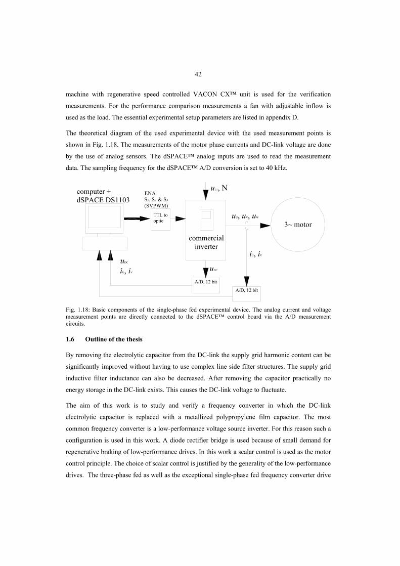
42
machine with regenerative speed controlled VACON CX™ unit is used for the verification
measurements. For the performance comparison measurements a fan with adjustable inflow is
used as the load. The essential experimental setup parameters are listed in appendix D.
The theoretical diagram of the used experimental device with the used measurement points is
shown in Fig. 1.18. The measurements of the motor phase currents and DC-link voltage are done
by the use of analog sensors. The dSPACE™ analog inputs are used to read the measurement
data. The sampling frequency for the dSPACE™ A/D conversion is set to 40 kHz.
computer + dSPACE DS1103
commercial inverter
3~ motoruU, uV, uW
iU, iV
uDC
A/D, 12 bit
A/D, 12 bit
ENAS1, S2 & S3
(SVPWM)
TTL to optic
uDC
iU, iV
uL1, N
Fig. 1.18: Basic components of the single-phase fed experimental device. The analog current and voltage measurement points are directly connected to the dSPACE™ control board via the A/D measurement circuits.
1.6 Outline of the thesis
By removing the electrolytic capacitor from the DC-link the supply grid harmonic content can be
significantly improved without having to use complex line side filter structures. The supply grid
inductive filter inductance can also be decreased. After removing the capacitor practically no
energy storage in the DC-link exists. This causes the DC-link voltage to fluctuate.
The aim of this work is to study and verify a frequency converter in which the DC-link
electrolytic capacitor is replaced with a metallized polypropylene film capacitor. The most
common frequency converter is a low-performance voltage source inverter. For this reason such a
configuration is used in this work. A diode rectifier bridge is used because of small demand for
regenerative braking of low-performance drives. In this work a scalar control is used as the motor
control principle. The choice of scalar control is justified by the generality of the low-performance
drives. The three-phase fed as well as the exceptional single-phase fed frequency converter drive

43
with a small DC-link capacitor are studied. Solving the problem of the capacitor’s life time by
replacing the electrolytic capacitor with the MPPF capacitor produces a new problem in the form
of the fluctuating DC-link voltage. When a very small capacitor is used every switching action
affects the DC-link voltage. By using only the scalar control it is guaranteed that motor control
does not generate any additional phenomena in supplied output voltage. For example the current
controllers in current vector control could cause additional fluctuation when combined with
fluctuating DC-link voltage. Thereby finding the origin of different voltage and current frequency
components and unexpected operation modes in VSI with small DC-link capacitor would be more
complicated. With scalar control no torque controllers are utilized. Thus, the interactions between
the modulation methods and the DC-link dynamics can be studied. This also justifies the use of
scalar control. The objective for this work is to study and develop a modulation strategy that
compensates the DC-link voltage fluctuation while the line side benefits are still preserved. In this
work, only the steady state motor operation is considered. No wide attention has been paid to the
transient operation. Although for the study induction motors have been used, the small DC-link
capacitor VSI does not limit the choice of the motor type to be used. The induction motor type is
chosen to be used for this study mainly because of its popularity in industrial applications.
In chapter 2 the “thoroughbred” three-phase fed frequency converter is studied. The fluctuating
DC-link voltage sets additional conditions to the frequency converter. These are to be taken into
consideration. While modulating the voltage to the motor, the DC-link fluctuation has to be
recalled. To roughly compensate the DC-link voltage fluctuation the traditional SVPWM method
has been employed. The SVPWM uses the DC-link voltage as feedforward information to form
the switching pattern beforehand. The measurements and simulation results are given for the
purposes of verifying the SVPWM method with the small DC-link capacitor VSI drive. The
problem with the SVPWM is that with a small DC-link capacitor the DC-link voltage
considerably changes even during the switching period. This is true especially when low
switching frequencies are used. To compensate the voltage variations during the switching period
a new method named Differential Space Vector PWM (DSVPWM) is introduced and studied. The
main idea of the DSVPWM method is that the stator voltage vector reference is converted to the
required change of the flux linkage reference during the switching period. During the switching
period the DC-link voltage waveform must be constantly observed in order to rapidly calculate
the actual achieved flux linkage change. The modulator thus uses active voltage vectors so as to
accomplish the reference flux linkage change. Simulation results are given for verification of the
DSVPWM.

44
Due to the DC-link fluctuation the linear modulation region ends earlier compared with a high-
capacitance DC-link capacitor VSI. This indicates that the overmodulation methods are one of the
main subjects for study. The total harmonic distortion for the VSI with small DC-link capacitor is
calculated and compared to the high-capacitance DC-link capacitor VSI. The overmodulation
methods for controlling the fundamental voltage starting from the linear modulation all the way to
the maximum available fundamental voltage are introduced, studied and tested.
Extra attention needs to be paid to the protection of the DC-link from power fed back from the
motor in case of braking. Under light loading condition or when the motor is braking the power
flow direction might be changed. Due to the small DC-link capacitor the DC-link voltage slew
rate is much higher compared to the traditional converter. Normally, the measured DC-link
voltage is used as a feedback to point out the state of braking. With a small DC-link capacitor the
DC-link voltage can raise intolerably high even during one switching period of the modulator
circuit. Therefore, when there is no speed encoder installed in the shaft, restraining the scalar
controlled motor drive from braking turns out to be a non-trivial task. To solve this problem, a
new overvoltage protection method based on the dynamic power factor control is introduced,
studied and tested. The introduced method is named as DPFC. Both the simulation and
measurement results are given to verify the DPFC functionality.
The DC-link capacitor combined with the line side inductance creates a resonance circuit.
Traditionally, the resonance frequency has been very low. Traditionally two decade lower than
switching frequency. Now, with the use of small DC-link capacitors and line side inductors, the
resonance frequency becomes significantly higher. The resonance frequency can be close to or
even higher than the switching frequency of the modulator. The resonance phenomenon is
studied. The study presents a great number of simulation and measurement results.
In chapter 3 the single-phase fed VSI is considered. The object of the work is to study a “very
much affordable” single-phase fed frequency converter for high inertia applications. The
assignment for this study was: Make a single-phase fed VSI that is very gentle to the supply grid
and which “as a by-product also rotates the motor”. The gentle grid behavior is gained with the
small DC-link capacitor. While loaded, the DC-link voltage follows the line voltage waveform.
This leads to a sinusoidal line current waveform, which is desirable. The main problem is thus to
make the motor rotate. The problem is approached using the traditional SVPWM combined with
the simple scalar control. With the SVPWM the main considerations are focused on the stator
voltage reference formation. The SVPWM variation, named as Flower Power by the author, is
introduced and verified by simulations and measurements. Also the traditional SVPWM type
45
modulator with estimated DC-link voltage feedforward is studied. The performance
measurements have been carried out using an adjustable fan load. It was presumed that due to the
heavily fluctuating torque the efficiency of the single-phase fed small DC-link capacitor VSI
could not be very satisfactory. The question remaining as to how good or bad this efficiency is
can only be solved in a study of the results acquired from test measurements. The performance
measurement results are compared with the results obtained with a commercial, unmodified
frequency converter. The single-phase fed small DC-link capacitor VSI creates a high torque
oscillation in the produced electric torque. The effect of the oscillating torque on the flexible shaft
has been studied and tested. The oscillation with low stiffness shaft couplings may result in
unintentional shaft deterioration due to the mechanical resonance.
All the simulation models included in the study are made by author. The measurement tests and
the off-line processing are carried out entirely by the author. The control algorithms included in
the simulations and the experimental devices are also produced by the author. Throughout the
study, the simulation and measurement results obtained are presented next to the corresponding
theoretical studies. The contributions of the study can be summarized as
The contributions
- Verification of the single and three-phase fed small DC-link capacitor VSI by simulations
and measurements
- Invention of the DSVPWM modulator
- Overvoltage protection based on dynamic power factor control (DPFC)
- Study of overmodulation and overmodulation method
- Study of the unorthodox single-phase fed VSI with simple modulator structure
The scientific conference publications including the above subjects
Sarén, H., Pyrhönen, O., 2005. Single Phase Fed Voltage Source Inverter with Small Dc-link Capacitor. 26th International PCIM Conference 7.-9.6.2005 Nuremberg, Power Electronics, Intelligent Motion, Power Quality. Conference cd.
Sarén, H., Pyrhönen, O., Rauma, K., Laakkonen, O., 2005. Overmodulation in Voltage Source Inverter with Small Dc-link Capacitor. IEEE 36th Annual Power Electronics Specialists Conference, 2005. Recife, Brazil. PESC05 conference cd. ISBN 0-7803-9034-2.
Sarén, H., Rauma, K., Pyrhönen, O. 2005. DTC Driven Single Phase Fed Voltage Source Inverter with Small DC-Link Capacitor. IEEE International Symposium on Industrial Electronics - ISIE 2005,20.-23.6.2005, Dubrovnik, Croatia, 2005.

46
Sarén, H., Pyrhönen, O., Luukko, J., Laakkonen, O., Rauma, K., 2005. Verification of Frequency Converter With Small Dc-link Capacitor. 11th European Conference on Power Electronics and Applications, EPE 2005. Dresden Germany. 11-14 Septemper 2005. ISBN 90-75815-08-5, Conference cd.
Patents or patent applications considering this topic
- EP Application 1511168, FI115265, DSVPWM
- FI Application number 20040838, Flower Power
- FI Application number 20041454, DPFC

47
2 THREE-PHASE FED VOLTAGE SOURCE INVERTER
In industry the three-phase AC is the most commonly used electricity source. In this chapter the
three-phase supplied frequency converter with a small DC-link capacitor is studied. Since the
research work has been accomplished with the objective of studying the effects of the fluctuating
DC-link voltage on the motor supply voltage, the scalar control has been used as the motor
control method. A considerable part of the research deals with the subject of modulation methods.
In the first part of this chapter, the principles of three-phase AC modulation are discussed. A new
differential space vector PWM (DSVPWM) method based on the idea of SVPWM is described
and verified. To compensate the DC-link voltage fluctuation, feedforward of the DC-link voltage
is necessary. In both the DSVPWM and SVPWM the DC-link voltage is used as the feedforward
signal. Finally, a modulation strategy is proposed.
After the study of three-phase AC modulation, overvoltage protection is discussed. Since there
exists, practically, no energy storage in the DC-link, the DC-link voltage may rise intolerably high
even during the single switching period due to the returning energy from the motor. Typically, no
external shaft pulse encoders are used. It is therefore necessary to find a method for identifying
the braking situation and protecting the VSI. A new method for that purpose, named Dynamic
Power Factor Control (DPFC), is introduced and verified by simulations and measurements.
The line side filter and DC-link capacitor together create a resonance circuit. Due to the small
DC-link capacitor and decreased AC-filter inductor the resonance frequency becomes
significantly high. The switching frequency of the inverter bridge works as a stimulus for the
resonance. This resonance phenomenon is studied at the end of this chapter.
2.1 Principles of the three-phase AC modulation
2.1.1 Space Vector PWM
In a traditional space vector modulation the correct switching instants and combination are
decided at the beginning of the switching period. The input for the space vector PWM is the stator
voltage vector reference in a stationary two-axis real and imaginary reference frame. The
reference voltage vector (1.6) can be written as a two-component vector with x and y as
yref,s,xref,s,refs, juuu += . (2.1)
The duration of the active voltage vectors Vm and Vm+1 in a current sector m during the switching
period Ts is calculated from the reference voltage vector as shown in
48
1s
1
srefs, +
++= mm
mm
Tt
Ttu VV , (2.2)
where the voltage vectors Vm and Vm+1 are defined as
( )
( )m
m
m
m
u
u
3π
j
DC1
13π
j
DC
e32
e32
=
=
+
−
V
V. (2.3)
The times for the active voltage vector are limited as
1s ++≥ mm ttT . (2.4)
The reference voltage is achieved by using the active voltage vectors Vm and Vm+1, with
corresponding durations tm and tm+1. The instantaneous length of the voltage vectors depend on the
DC-link voltage uDC as |V|=2/3uDC. It is worth to point out that in SVPWM the DC-link voltage is
assumed to be constant during the switching period. In the low-speed region where no
overmodulation is used, the maximum radius for the circular reference voltage vector is
323 DCrefs, uu == V . The SVPWM method is illustrated in Fig. 2.1, where the eight
discrete voltage vectors Vm and the circle describing the maximum available voltage vector are
shown. Also the xy-coordinate system based on the real and imaginary components is shown. The
voltage vectors are defined by a combination of the conducting and non-conducting switches S1,
S2 and S3 in the inverter bridge. The conducting and non-conducting mode is denoted with logic 1
and 0 respectively. Six of the voltage vectors, subscripts m=1, 2,…, 6, are active and two of
them, subscripts m=0, 7, represent zero-vectors. The active voltage vectors are forming 6
sectors of equal size numbered as m=1, 2,…, 6. The SVPWM locally averages the adjacent and
zero-vectors to be equal to the reference vector over the switching period Ts. This is illustrated in
Fig. 2.2.

49
V0,7V4
V1
m=4 m=6
V6
m=5V5
m=3 m=1
V2m=2V3
23
( ) =321 S,S,S ( )0,0,1
( )0,1,1( )0,1,0
( )1,1,0
( )1,0,0 ( )1,0,1
( )( )0,0,0
1,1,1
DC32 u=V
x
y
Fig. 2.1: The eight discrete voltage vectors Vm defined by the logic states of power switches. Six of the voltage vectors, subscripts m=1, 2,…, 6, are active and two of them, subscripts m=(0, 7), represent zero-vectors. The active voltage vectors are forming 6 sectors of equal size numbered as m=1, 2,…, 6. The
maximum voltage circle radius is mV2/3 .
V1
V2
m=1
refs,u
1s
1 V ++
mm
Tt
mm
Tt V
s
xxref,s,u
yref,s,u
y
Fig. 2.2: The formulation of the average voltage vector reference us,ref is done by combining in the current sector m two active vectors with corresponding durations tm and tm+1 during the switching period Ts. Zero-vectors are used the remaining time.
From (2.1) and (2.2) it is possible to calculate the durations tm and tm+1 needed to fulfill the
reference values for the components of the stator voltage vector

50
( ) ( )⎥⎦
⎤⎢⎣
⎡
⎥⎥⎥⎥
⎦
⎤
⎢⎢⎢⎢
⎣
⎡
⎟⎠⎞
⎜⎝⎛ −⎟
⎠⎞
⎜⎝⎛ −−
⎟⎠⎞
⎜⎝⎛−⎟
⎠⎞
⎜⎝⎛
=⎥⎦
⎤⎢⎣
⎡
+ yref,s,
xref,s,
DC
s
1 13πcos1
3πsin
3πcos
3πsin3
uu
mm
mm
uT
tt
m
m . (2.5)
The remaining switching period is left for the zero-vectors V0 and V7. The duration for the zero-
vectors is calculated from
( )170 ++−=+= mmszero ttTttt . (2.6)
Furthermore, the durations of the active vectors can be transformed for each phase into switching
instants. In Fig. 2.3 one switching sequence is shown. The active vectors are distributed
symmetrically in time.
22222222017710 tttttttt mmmm ++
1S
2S
3S
sT
017710 VVVVVVVV mmmm ++
0
0
1
0
1
1
1
1
1
1
1
1
0
1
1
0
0
1
0
0
0
0
0
0
onU,t
onV,t
onW,t
Fig. 2.3: Formulation of the switching pattern during the switching period Ts. The switching sequence starts with zero-vectors V0. After that, the first active vector Vm is selected and hold over the pre-calculated time length tm/2. The second active vector Vm+1 is selected after the first active voltage vector time is reached. The second zero-voltage vector V7 is selected after the second active voltage vector pre-calculated time tm+1/2 is reached. After the first half of the switching period is gone through, the switching combination is reversed.

51
The calculation for the active time for the particular phase U, V, W depends on the sector. In
Table 2.1 the time instant for turning on the corresponding phase is shown.
Table 2.1: The time instant for turning on the corresponding phase as a function of the sector.
Sector, m onU,t onV,t onW,t
1 20t 220 mtt + 222 10 +++ mm ttt
2 22 10 ++ mtt 20t 222 10 +++ mm ttt
3 222 10 +++ mm ttt 20t 220 mtt +
4 222 10 +++ mm ttt 22 10 ++ mtt 20t
5 220 mtt + 222 10 +++ mm ttt 20t
6 20t 222 10 +++ mm ttt 22 10 ++ mtt
The time to turn off the switch of the corresponding phase can be calculated from
on,soff, ii tTt −= , (2.7)
where WV,U,=i .
In some cases, it is convenient to denote the phase references with duty cycles. The duty cycle
indicates the amount of active time of the switch with respect to the switching period. The duty
cycle D for the corresponding phase can be calculated from
s
on,21T
tD i
i −= , (2.8)
where the output phase label is denoted as WV,U,=i and D∈[0,1].
The distribution of the zero-time between the zero-vectors t0 and t7 can be freely chosen. The use
of only one zero-vectors leads to a situation where one phase is clamped into one of the DC-buses
through the whole switching sequence. According to the research done by Holmes (1996) an even
distribution of the zero-time between two zero-vector, that is t0=t7, results in a smaller motor
phase current ripple. An even distribution of the zero-vectors results in a situation that is

52
comparable to the triangle-comparison with triple frequency component (Blasko, 1997). In this
work even distribution of zero-vectors in SVPWM is used due to the aim of smaller motor phase
current ripple (Holmes, 1996).
2.1.2 Overmodulation
The zero-vector time decreases as the stator voltage vector amplitude increases. The sinusoidal
output quantities are retained when the zero-vectors are present in the space vector modulation.
This modulation mode is called linear modulation. After this point, the overmodulation methods
are needed. Overmodulation is used to increase the voltage output of the PWM controlled
frequency converter. It is important to use the full frequency converter voltage because, in using
the full frequency converter voltage, it is possible to both reduce the cost and increase the output
power. Furthermore, an electric drive with high overmodulation performance is less sensitive to
DC-link voltage disturbances.
A DC-link voltage sag may lead in an unintentional entering to the overmodulation region. The
DC-link sag is a result of the line voltage sag or fault conditions of electric drive. When smaller
DC-link capacitors are used, voltage sags caused by the full-wave rectifier bridge are present all
the time. Under such conditions, a high performance overmodulation method could maintain the
drive performance as much as possible. The inverter blanking time and minimum-pulse-width
constraints could further reduce the linearity range. For reasons of simplicity, the following study
of overmodulation does not take into consideration the blanking time and minimum-pulse-width
limitations.
The modulation index M is used to describe the voltage utilization of the modulator. Here, similar
to the reference of Holtz (1993), the modulation index is defined with the magnitude of the
fundamental voltages of the inverter output voltage uf and the theoretical maximum voltage under
six-step operation -stepsixu = DCπ2 u . For a given DC-link voltage uDC, the modulation index M is
defined as
DC
f
step-six
f
π2 u
uu
uM == . (2.9)
In the linear modulation region the stator voltage reference does not exceed the maximum
available voltage circle. When a big DC-link capacitor is used the DC-link voltage, essentially,
remains constant. The constant DC-link voltage results in a hexagon-shaped maximum available
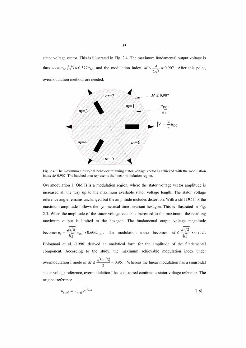
53
stator voltage vector. This is illustrated in Fig. 2.4. The maximum fundamental output voltage is
thus DCDCf 577.03 uuu ≈= and the modulation index 907.032
π≈≤M . After this point,
overmodulation methods are needed.
m=4 m=6
m=5
m=3m=1
m=2
DC32V u=
3DCu
907.0≤M
Fig. 2.4: The maximum sinusoidal behavior retaining stator voltage vector is achieved with the modulation index M≤0.907. The hatched area represents the linear modulation region.
Overmodulation I (OM I) is a modulation region, where the stator voltage vector amplitude is
increased all the way up to the maximum available stator voltage length. The stator voltage
reference angle remains unchanged but the amplitude includes distortion. With a stiff DC-link the
maximum amplitude follows the symmetrical time invariant hexagon. This is illustrated in Fig.
2.5. When the amplitude of the stator voltage vector is increased to the maximum, the resulting
maximum output is limited to the hexagon. The fundamental output voltage magnitude
becomes DCDC4f 606.03
π2uuu ≈= . The modulation index becomes 952.0
3
2π4
≈≤M .
Bolognani et al. (1996) derived an analytical form for the amplitude of the fundamental
component. According to the study, the maximum achievable modulation index under
overmodulation I mode is ( ) 951.02
3ln3≈≤M . Whereas the linear modulation has a sinusoidal
stator voltage reference, overmodulation I has a distorted continuous stator voltage reference. The
original reference
refs,jrefs,refs, e θuu = [1.6]

54
is reformulated into
refs,jlimref,s,OMIref,s, e θuu = , (2.10)
where subscript lim stands for limited quantity.
m=4 m=6
m=5
m=3m=1
m=2
DC32V u=
DC4 3
π2u
952.0≤M
Fig. 2.5: The maximum stator voltage vector under overmodulation I. When the modulator uses all the available voltage limiting only the amplitude to the voltage hexagon, a modulation index up to M≤0.952 is achieved. The modulated voltage is continuous but due to the amplitude limitations it includes distortion.
Under linear modulation the fundamental output voltage is expected to increase linearly as a
function of the voltage vector reference amplitude. The limit is 3DCu . After this point
overmodulation I is used and according to Bolognani et al. (1996) the fundamental voltage output
OMIf,u can be calculated as a function of the DC-link voltage uDC and stator voltage vector
amplitude refs,u .
( )⎟⎟⎠
⎞⎜⎜⎝
⎛⎟⎟⎠
⎞⎜⎜⎝
⎛⎟⎟⎠
⎞⎜⎜⎝
⎛−+=
23πtanln
3π6 gDC
grefs,refs,OMIf,
αα
uuuu , (2.11)
where
55
( )
32
3
3cos6π
DCrefs,
DC
refs,
DC
1refs,g
uuu
u
u
u
≤≤
⎟⎟⎟⎟
⎠
⎞
⎜⎜⎜⎜
⎝
⎛
−= −α. (2.12)
After overmodulation I has reached the upper limit, overmodulation II (OM II) becomes active.
Under overmodulation II the essential feature is that the particular active voltage vector that is
closest to the stator voltage reference vector is used gradually longer and longer time periods. In
the final state the method called six-step is applied, which means that each state vector is used one
sixth of the fundamental period. Whereas the linear modulation has a sinusoidal stator voltage
reference, overmodulation I has a distorted continuous stator voltage reference. While
overmodulation I has a distorted continuous stator voltage reference, overmodulation II has a
distorted discontinuous stator voltage reference. The absolute maximum fundamental voltage
available from the VSI is achieved under sixstep operation.
Under overmodulation II the controller affects both the amplitude and angle of the stator voltage
reference vector. The original stator voltage vector reference (1.6) is reformulated into
limref,s,jlimref,s,OMIIref,s, e θuu = . (2.13)
In the overmodulation II method, shown in Holtz et al. (1993), the trajectory of the refs,u is
limited to the hexagon while the angle is defined as a function of the hold-angle hα . The hold-
angle is a function of the modulation index, that is ( )Mf=hα . The value of the hold-angle is
limited between [0… 6π ]. The value hα = 6π equals the sixstep mode. The controlled, limited
stator voltage vector reference angle limref,s,θ can be calculated from
( )( )
⎪⎪⎪
⎩
⎪⎪⎪
⎨
⎧
≤≤−
−≤≤−
−≤≤
=
.3π
3π
3π
3π
6ππ
00
refs,h
hrefs,hh
hrefs,
hrefs,
limref,s,
θα
αθαα
αθαθ
θ (2.14)
More about overmodulation methods can be found from literature. Holtz (1992, 1993, 1994) and
Kerkman (1993, 1995, 1996), for example, are authors who have treated the subject in several

56
studies that are widely referred to in the literature. One of the most comprehensive survey and
research works on overmodulation is done by Hava (1998). In the study by Tarkiainen (2005) the
modulation index and fundamental voltage produced by the DTC is introduced.
Fig. 2.6 shows the usage of the modulation methods and the index of the achievable modulation.
907.0952.0
1
≈≈
4444 34444 21
modulationlinear
43421
I modulation-over
43421
II modulation-over
0 refs,u
M
Fig. 2.6: Modulation methods and the index of the modulation. Under linear modulation the stator voltage vector reference does not need to be limited by the modulator in any way. The modulation index 0.907 can be achieved by using linear modulation. With overmodulation I the modulation index can be increased to 0.952, however at the expense that the limitations of the stator voltage vector amplitude will cause distortion. Overmodulation II is used to further increase the modulation index up to the theoretical maximum value of 1. The limitations in the stator voltage vector reference influence both the stator voltage vector amplitude and angle.
2.1.3 Analytical estimation of the DC-link voltage fluctuation
Kretschmar et al. (1998) have studied the DC-link fluctuation. They divide fluctuation into two
parts depending on the fluctuation source. The first part is the fluctuation caused by the full-wave
diode rectifier bridge. The mean value of the DC-link voltage uDC,mean gained from the rectifier
bridge is
,pu 1.65V540
π23
nmeanDC,
≈≈
= Uu
(2.15)
where Un is the nominal line-to-line RMS voltage. For the numerical evaluation the value of Un
was set to 400 V.
The fluctuation caused by the rectifier recDC,u∆ can be calculated from
57
pu 0.23V76
232 nrecDC,
≈≈
⎟⎟⎠
⎞⎜⎜⎝
⎛−=∆ Uu
. (2.16)
According to Kretschmar et al. (1998) the DC-link voltage fluctuation caused by the inverter
bridge invDC,u∆ can be represented by means of the steady state power P, the DC-link voltage
mean value UDC and the switching period Ts as
DC
sinvDC, 8
2π4
CUPTM
u−
=∆ . (2.17)
Hence, the modulation index used in Kretschmar et al. (1998) is scaled here to be equivalent to
the modulation index based on the six-step unity modulation index, which is used in this work.
The equation can thus be considered only up to the modulation index M=π/4, which is the upper
limit of the analog realized PWM without an added third harmonic component in the carrier
signal.
The total peak-to-peak worst case for DC-link voltage fluctuation DCu∆ can be estimated by
summing the fluctuations due to the rectifier and inverter bridge as
invDC,recDC,DC 2 uuu ∆+∆=∆ , (2.18)
where the fact that the inverter bridge fluctuation invDC,u∆ can be both negative and positive is
noticed. A more precise formulation and explanations of the equations are presented in the
original reference (Kretschmar et al., 1998).
2.1.4 Verification of the small DC-link capacitor VSI
To verify the idea of the small DC-link capacitor VSI, simulations have been carried out. Scalar
control and a SVPWM modulator with 100 µs switching period Ts yielding a 10 kHz switching
frequency swf has been used. The nominal torque and half of the nominal mechanical speed has
been used, that means the power P becomes 2 kW. A 2 µF capacitor has been used as the DC-link
capacitor C. The DC-link voltage has been used as the feedforward in the SVPWM. Fig. 2.7
shows simulation results of one line current igrid, the DC-link capacitor current iC and the DC-link
voltage uDC waveforms with corresponding FFT-figures. For the purpose of simulation model
verification, the same situation was created with an experimental device. In Fig. 2.8 a measured

58
line current igrid, DC-link capacitor current iC and the DC-link voltage uDC are shown. The
corresponding FFT-figures are also shown. Comparison between simulation results and
experimental device measurement results clearly shows the accuracy of the simulation model.
Another much desired feature, present in both the simulated and measured supply grid current, is
the frequency content shown in the FFT. As can be seen, the supply grid current harmonic content
is much friendlier to the line properties compared with traditional frequency converters. By
substituting the values obtained from the identical simulations and measurements discussed above
the estimated fluctuation due to the inverter bridge can be estimated analytically from (2.17).
With half the nominal speed the modulation index becomes
45.0
π2
321
DC
DC
≈=u
u
M (2.19)
and the fluctuation due to the inverter bridge can be evaluated as
pu1.0
V33invDC,
≈
≈∆u. (2.20)
The result is in good accordance with the simulated (Fig. 2.7) and measured (Fig. 2.8) DC-link
voltage fluctuation. Hence, the fluctuation caused by the inverter bridge is distributed mainly to
the switching frequency with a component of approximately 10 V and to the second harmonic
component of the switching frequency with a component of approximately 20 V. The result of the
fluctuation due to the rectifier bridge, given in (2.16), can be scaled to equal the FFT values
shown in the figures. The FFT value represents the peak value of the corresponding sinusoidal
signal. Thus, the fluctuation originating from the diode rectifier bridge, shown in (2.16), becomes
V382ˆ recDC,recDC, =∆=∆ uu when scaled to correspond the result given in the figures. The
fluctuation amplitudes recDC,u∆ and invDC,u∆ are in good accordance with the simulation and
measurement results. The analytically evaluated DC-link voltage fluctuations described in
Kretschmar et al. (1998) show the scalability of the analytic equations for different sizes of the
DC-link capacitor. Thus, the equations (2.16) and (2.17) can be used to approximate the DC-link
capacitor size required to limit the DC-link voltage fluctuation to an acceptable level.
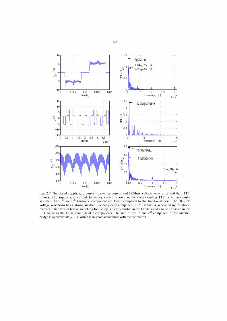
59
0 0.005 0.01 0.015 0.02−10
−5
0
5
10
time [s]
i grid
[A
]
0 0.5 1 1.5 2
x 104
0
0.5
1
1.5
frequency [Hz]
FFT
of
i grid
0 0.5 1 1.5 2 2.5 3 3.5 4
x 10−4
−15
−10
−5
0
5
10
15
time [s]
i C [
A]
0 2 4 6
x 105
0
0.5
1
1.5
2
2.5
frequency [Hz]
FFT
of
i C
0 0.005 0.01 0.015 0.02400
450
500
550
600
650
time [s]
u DC
[V
]
0.03 0.5 1 1.5 2
x 104
0
20
40
60
80
frequency [Hz]
FFT
of
u DC
540@0Hz
6@50Hz
5.25@20kHz
20@20kHz
1.04@250Hz 0.98@350Hz
50@300Hz
Fig. 2.7: Simulated supply grid current, capacitor current and DC-link voltage waveforms and their FFT figures. The supply grid current frequency content shown in the corresponding FFT is as previously assumed. The 5th and 7th harmonic component are lower compared to the traditional case. The DC-link voltage waveform has a strong six-fold line frequency component of 50 V that is generated by the diode rectifier. The inverter bridge switching frequency is clearly visible in the DC-link and can be observed in the FFT figure as the 10 kHz and 20 kHz components. The sum of the 1st and 2nd component of the inverter bridge is approximately 30V which is in good accordance with the estimation.
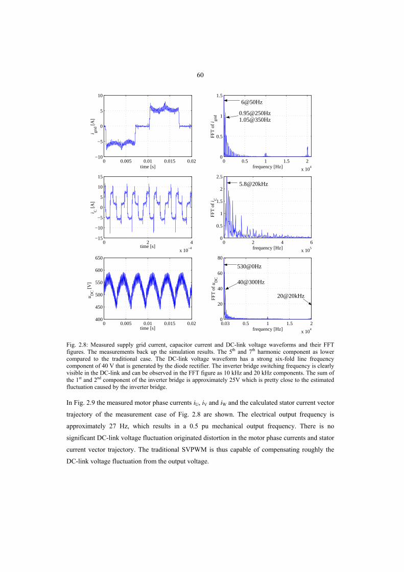
60
0 0.005 0.01 0.015 0.02−10
−5
0
5
10
time [s]
i grid
[A
]
0 0.5 1 1.5 2
x 104
0
0.5
1
1.5
frequency [Hz]
FFT
of
i grid
0 2 4
x 10−4
−15
−10
−5
0
5
10
15
time [s]
i C [
A]
0 2 4 6
x 105
0
0.5
1
1.5
2
2.5
frequency [Hz]
FFT
of
i C
0 0.005 0.01 0.015 0.02400
450
500
550
600
650
time [s]
u DC
[V
]
0.03 0.5 1 1.5 2
x 104
0
20
40
60
80
frequency [Hz]
FFT
of
u DC
6@50Hz
5.8@20kHz
530@0Hz
20@20kHz
0.95@250Hz 1.05@350Hz
40@300Hz
Fig. 2.8: Measured supply grid current, capacitor current and DC-link voltage waveforms and their FFT figures. The measurements back up the simulation results. The 5th and 7th harmonic component as lower compared to the traditional case. The DC-link voltage waveform has a strong six-fold line frequency component of 40 V that is generated by the diode rectifier. The inverter bridge switching frequency is clearly visible in the DC-link and can be observed in the FFT figure as 10 kHz and 20 kHz components. The sum of the 1st and 2nd component of the inverter bridge is approximately 25V which is pretty close to the estimated fluctuation caused by the inverter bridge.
In Fig. 2.9 the measured motor phase currents iU, iV and iW and the calculated stator current vector
trajectory of the measurement case of Fig. 2.8 are shown. The electrical output frequency is
approximately 27 Hz, which results in a 0.5 pu mechanical output frequency. There is no
significant DC-link voltage fluctuation originated distortion in the motor phase currents and stator
current vector trajectory. The traditional SVPWM is thus capable of compensating roughly the
DC-link voltage fluctuation from the output voltage.
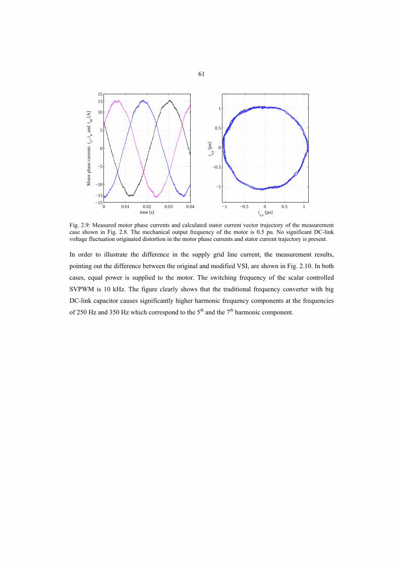
61
0 0.01 0.02 0.03 0.04−15
−13
−10
−5
0
5
10
13
15M
otor
pha
se c
urre
nts
i U, i
V a
nd i
W [
A]
time [s]−1 −0.5 0 0.5 1
−1
−0.5
0
0.5
1
i s,y [
pu]
is,x
[pu] Fig. 2.9: Measured motor phase currents and calculated stator current vector trajectory of the measurement case shown in Fig. 2.8. The mechanical output frequency of the motor is 0.5 pu. No significant DC-link voltage fluctuation originated distortion in the motor phase currents and stator current trajectory is present.
In order to illustrate the difference in the supply grid line current, the measurement results,
pointing out the difference between the original and modified VSI, are shown in Fig. 2.10. In both
cases, equal power is supplied to the motor. The switching frequency of the scalar controlled
SVPWM is 10 kHz. The figure clearly shows that the traditional frequency converter with big
DC-link capacitor causes significantly higher harmonic frequency components at the frequencies
of 250 Hz and 350 Hz which correspond to the 5th and the 7th harmonic component.

62
0 0.005 0.01 0.015 0.02 0.025 0.03 0.035 0.04−20
−10
0
10
20
time [s]
Supp
ly g
rid
curr
ent [
A]
50 250 350 550 650 800 1000 1200 1400 1600 1800 20000
2
4
6
8
10
12
frequency [Hz]
FFT
of
supp
ly g
rid
curr
ent
modified VSI with small dc−link capacitor: LAC
=0.4mH , C=2µF
original VSI: LAC
=3.4mH, C=165µF
modified VSI with small dc−link capacitor: LAC
=0.4mH , C=2µF
original VSI: LAC
=3.4mH, C=165µF
Fig. 2.10: Measured supply grid current for a standard commercial high-capacitance frequency converter (LAC= 3.4 mH, C= 165 µF) and for a frequency converter with small DC-link capacitor (LAC= 0.4 mH, C= 2 µF). The corresponding FFT figures are shown. The supply grid current wave forms differ greatly from each other. The VSI with small DC-link capacitor generates smaller harmonic frequency components at the frequencies of 250 Hz and 350 Hz which correspond to the 5th and the 7th harmonic component.
2.2 Improvement of modulation in the small DC-link capacitor VSI
To compensate the DC-link fluctuation during the switching sequence, a new method called
DSVPWM is introduced. Also changes in the overmodulation behavior are considered later in this
chapter.
2.2.1 Differential SVPWM (DSVPWM)
Dc-link voltage fluctuation naturally affects the maximum available instantaneous stator voltage
vector (Fig. 2.11). Especially at low switching frequency the DC-link voltage differs significantly
from the measured uDC during the switching period Ts. That is why the traditional space vector
PWM cannot work accurately under heavily fluctuating DC-link voltage.

63
V5 V6
V0,7V4
V3 V2
V1
fluctuating DCu
Fig. 2.11: The behavior of six discrete voltage vectors and the largest voltage circle under fluctuating DC-link voltage. The fluctuation of the DC-link voltage takes the shape of pulsating active voltage vectors. At a certain time instant the DC-link voltage level determines the length of the active vectors to 2/3uDC. In the figure, four different lengths of active voltage vectors are shown with the corresponding values of DC-link voltage.
The new concept, named differential SVPWM (DSVPWM), is based on the needed change of the
flux linkage ψ∆ during the switching period Ts. The change of the flux linkage reference can be
derived from (2.2) by multiplying both sides of the equation by Ts. The reference value is updated
once per switching cycle. The calculation of the reference for the flux linkage change is shown in
1
srefs,refs,
11srefs,
+
++
∆+∆=
=∆
+=
mm
mmmm
ψψ
TuψttTu VV
(2.21)
By substituting (2.3) into (2.21) we get the reference change for the flux linkage for both active
vectors Vm and Vm+1 in the current sector m
( ) ( )m
m
m
m
mmmm
utut
ttψ
3π
j
DC1
13π
j
DC
11refs,
e32e
32
+
−
++
+=
+=∆ VV. (2.22)
Now the reference for the change of the flux linkage amplitude during the switching period in
sector m is defined as
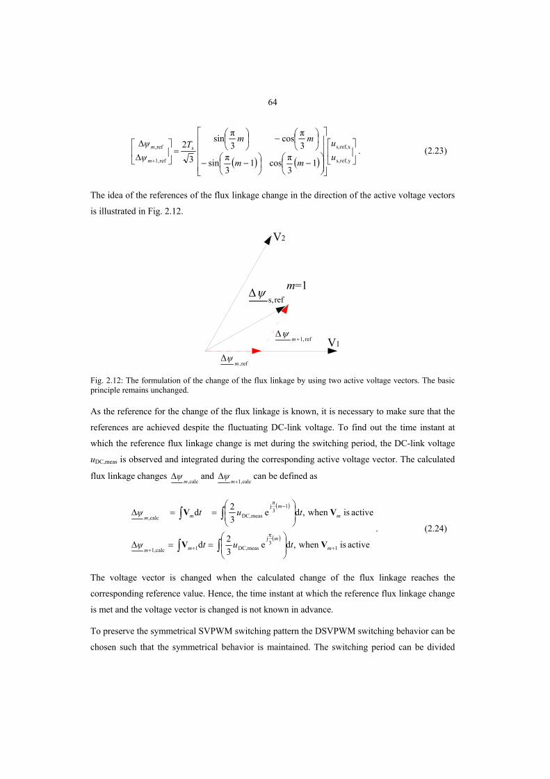
64
( ) ( )⎥⎦
⎤⎢⎣
⎡
⎥⎥⎥⎥
⎦
⎤
⎢⎢⎢⎢
⎣
⎡
⎟⎠⎞
⎜⎝⎛ −⎟
⎠⎞
⎜⎝⎛ −−
⎟⎠⎞
⎜⎝⎛−⎟
⎠⎞
⎜⎝⎛
=⎥⎦
⎤⎢⎣
⎡∆∆
+ yref,s,
xref,s,s
ref1,
ref,
13πcos1
3πsin
3πcos
3πsin
32
uu
mm
mmTψψ
m
m . (2.23)
The idea of the references of the flux linkage change in the direction of the active voltage vectors
is illustrated in Fig. 2.12.
m=1
V2
V1
refs,ψ∆
ref1,+∆
mψ
ref,∆
mψ
Fig. 2.12: The formulation of the change of the flux linkage by using two active voltage vectors. The basic principle remains unchanged.
As the reference for the change of the flux linkage is known, it is necessary to make sure that the
references are achieved despite the fluctuating DC-link voltage. To find out the time instant at
which the reference flux linkage change is met during the switching period, the DC-link voltage
uDC,meas is observed and integrated during the corresponding active voltage vector. The calculated
flux linkage changes calc,m
ψ∆ and calc1,+
∆m
ψ can be defined as
( )
( )active is when,de
32d
active is when,de32d
13π
j
measDC,1calc1,
13πj
measDC,calc,
+++
−
∫∫
∫∫
⎟⎟⎠
⎞⎜⎜⎝
⎛==∆
⎟⎟⎠
⎞⎜⎜⎝
⎛==∆
m
m
mm
m
m
mm
tutψ
tutψ
VV
VV
. (2.24)
The voltage vector is changed when the calculated change of the flux linkage reaches the
corresponding reference value. Hence, the time instant at which the reference flux linkage change
is met and the voltage vector is changed is not known in advance.
To preserve the symmetrical SVPWM switching pattern the DSVPWM switching behavior can be
chosen such that the symmetrical behavior is maintained. The switching period can be divided

65
into two sections: Section 1 is from 0 to Ts/2 and section 2 is from Ts/2 to Ts. During the first
period the halved values of the flux linkage changes are fulfilled. The switching sequence goes as
follows: The first active voltage vector Vm is chosen at the beginning of the switching period Ts.
The vector is kept until the limit of ½ ref,mψ∆ is achieved. After that, the second active voltage
vector Vm+1 is chosen and kept until the reference of ½ ref,1+∆ mψ is achieved. After both active
vectors are used, the zero-vector V7 is kept until the switching period reaches halfway Ts/2. After
half of the switching period is accomplished, the sequence is reversed and the second active
voltage vector Vm+1 is chosen. The vector is kept until the second half of the flux linkage change
½ ref,1+∆ mψ is met. After that, the first active voltage vector Vm is used until the reference flux
change ½ ref,mψ∆ is reached. After that, the zero-vector V0 is used until the end of the switching
sequence. A theoretical drawing of the DSVPWM switching sequence is shown in Fig. 2.13.
2sT
0 sT
mV 1+mV 7V mV1+mV 0V
∫ tmdV ∫ + tm d1V ∫ tmdV∫ + tm d1V
ref,calc, 21
21
mm ψψ ∆=∆
ref,calc, 21
21
mm ψψ ∆=∆ref1,calc1, 21
21
++ ∆=∆ mm ψψ
ref1,calc1, 21
21
++ ∆=∆ mm ψψ
Fig. 2.13: The switching sequence of the DSVPWM. Differently from the SVPWM, the DSVPWM switching sequence begins with the active voltage vector. The first active voltage vector Vm is chosen at the beginning of the switching period Ts. The vector is kept until the limit of ½ ref,mψ∆ is achieved. After that,
the second active voltage vector Vm+1 is chosen and kept until the reference of ½ ref,1+∆ mψ is achieved. After both active vectors are used, the zero-vector V7 is kept until the switching period reaches halfway Ts/2. After half of switching period is accomplished, the sequence is reversed and the second active voltage vector Vm+1 is chosen. The vector is kept until the second half of the change of flux linkage change ½ ref,1+∆ mψ is
met. After that, the first active voltage vector Vm is used until the reference flux change ½ ref,mψ∆ is reached. After that, the zero-vector V0 is used until the end of the switching sequence.
The references for the flux linkage changes can be updated in the middle of the switching period
Ts/2. If the switching frequency is low, updating the references in the middle of the switching
period improves the accuracy of the produced voltage.
During the switching period, both references refm,
ψ∆ and ref1,+
∆m
ψ are being fulfilled. Thus, we
achieve the voltage reference refs,u given by the upper controllers despite the fluctuating DC-link
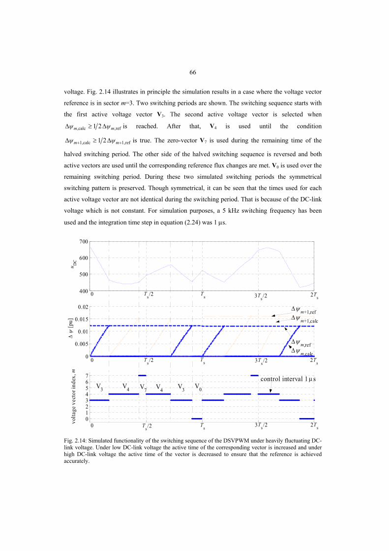
66
voltage. Fig. 2.14 illustrates in principle the simulation results in a case where the voltage vector
reference is in sector m=3. Two switching periods are shown. The switching sequence starts with
the first active voltage vector V3. The second active voltage vector is selected when
ref,,calc 21 mm ψψ ∆≥∆ is reached. After that, V4 is used until the condition
ref1,1,calc 21 ++ ∆≥∆ mm ψψ is true. The zero-vector V7 is used during the remaining time of the
halved switching period. The other side of the halved switching sequence is reversed and both
active vectors are used until the corresponding reference flux changes are met. V0 is used over the
remaining switching period. During these two simulated switching periods the symmetrical
switching pattern is preserved. Though symmetrical, it can be seen that the times used for each
active voltage vector are not identical during the switching period. That is because of the DC-link
voltage which is not constant. For simulation purposes, a 5 kHz switching frequency has been
used and the integration time step in equation (2.24) was 1 µs.
400
500
600
700
0
0.005
0.01
0.015
0.02
∆ ψ
[pu]
01234567
volta
ge v
ecto
r ind
ex, m
uD
C
∆ψ m+1,ref ∆ψ m+1,calc ∆ψ m,ref ∆ψ m,calc
V3 V4 V7 V4 V3 V0
Ts
Ts
Ts
Ts/2
Ts/2
Ts/2
3Ts/2
3Ts/2
2Ts
3Ts/2
2Ts
2Ts
0
0
0
control interval 1 µs
Fig. 2.14: Simulated functionality of the switching sequence of the DSVPWM under heavily fluctuating DC-link voltage. Under low DC-link voltage the active time of the corresponding vector is increased and under high DC-link voltage the active time of the vector is decreased to ensure that the reference is achieved accurately.

67
To illustrate the superiority of the DSVPWM modulation method simulations have been carried
out for the purpose of comparing the DSVPWM with the SVPWM. In the simulations, both
modulation methods are exposed to DC-link voltage fluctuation. The reference vector amplitude
is kept at 0.5 pu while the stator voltage vector angle reference is varied from 0 to π/3 at the steps
of π/60. A switching frequency of 5 kHz is used. In each simulation, the reference voltage vector
is kept in a constant position for multiple switching periods while the DC-link voltage is
fluctuating. The error in the resulting modulated voltage vector over a switching period of 200 µs
is calculated. The produced average voltage vector, denoted with subscript act, can be found by
integrating the DC-link voltage during the corresponding active voltage vector as shown below
activeiswhen,d321
activeiswhen,d321
10
DCs
act,1
0DC
sact,
s
s
++ ∫
∫
=
=
m
T
m
m
T
m
tuT
u
tuT
u
V
V. (2.25)
The produced voltage vector act,su in the stator reference frame is then calculated from
( )
( )⎥⎦
⎤⎢⎣
⎡
⎥⎥⎥⎥
⎦
⎤
⎢⎢⎢⎢
⎣
⎡
⎟⎠⎞
⎜⎝⎛
⎟⎠⎞
⎜⎝⎛ −
⎟⎠⎞
⎜⎝⎛
⎟⎠⎞
⎜⎝⎛ −
=⎥⎦
⎤⎢⎣
⎡=
+ act,1
act,
y,acts,
x,acts,act,s
3πsin
3π1sin
3πcos
3π1cos
m
m
uu
mm
mm
uu
u . (2.26)
Fig. 2.15 and Fig. 2.16 demonstrate the error calculation. Three switching sequences are shown in
both of the figures from which it is clear that the SVPWM modulator is not able to fulfill the
references accurately during the switching period (Fig. 2.15). Small but still significant errors
between the corresponding reference and actual values can be found. In the case of DSVPWM,
the error is significantly smaller and the actual voltages match with the references (Fig. 2.16).

68
1.3
1.4
1.5
1.6
1.7
1.8
u DC
[pu
]
0 1 2 3 4 5 6
x 10−4
0
0.1
0.2
0.3
0.4
0.5
time [s]
Act
ual u
m,a
ct a
nd u
m+
1,ac
t
V0 V
m V
m+1 V
7 V
m+1 V
m V
0
um,ref
um+1,ref
error
error
Fig. 2.15: Simulated realization of the modulated voltage vector with the SVPWM modulator under heavily fluctuating DC-link voltage. The SVPWM creates a significant error. The error can be seen at the end of the switching sequences at the time instants 200 µs, 400 µs and 600 µs. The produced voltage vectors um,act and um+1,act do not meet accurately their corresponding reference levels during the switching sequence.
1.4
1.5
1.6
1.7
1.8
u DC
[pu
]
0 1 2 3 4 5 6
x 10−4
0
0.1
0.2
0.3
0.4
0.5
time [s]
Act
ual u
m,a
ct a
nd u
m+1
,act
Vm
Vm+1
V7 V
m+1 V
m V
0
um+1,ref
um,ref
Fig. 2.16: Simulated realization of the modulated voltage vector with the DSVPWM modulator under heavily fluctuating DC-link voltage. The DSVPWM compensates the DC-link fluctuation caused error. The produced voltage vectors um,act and um+1,act do meet accurately their corresponding reference levels during the switching sequences of 0 to 200 µs, 200 µs to 400 µs and 400µs to 600 µs.

69
Fig. 2.17 shows the variations of the resulting voltage vector time-averages produced by the
SVPWM and the DSVPWM during multiple switching periods with different reference angles.
With the SVPWM modulator the DC-link fluctuation causes error in the realization of the stator
voltage vector whereas with the DSVPWM method the produced voltage follows the reference
value with good accuracy.
0 20 40 60 80 100 120 140 160 1800
20
40
60
80
100
120
140
160
us,x
[V]
u s,y [
V]
BLUE =DSVPWM, ideal u
DC feedback
m=1 u
B=√(2/3)⋅400 V
|u
s,ref|=0.5⋅u
B = 163 V
fsw
=5 kHz
RED =SVPWM
Fig. 2.17: Simulated realization of modulated voltage vector with the SVPWM and DSVPWM modulators under heavily fluctuating DC-link voltage. The SVPWM creates in this case a significant 14 V amplitude error while DSVPWM compensates totally the DC-link fluctuation caused error.
So far, only the linear modulation region is covered with DSVPWM method. The use of the
DSVPWM in the overmodulation region produces an error in the average voltage vector angle.
The amplitude is limited to the hexagon. This is illustrated in the Fig. 2.18, where an overlong
stator voltage vector reference us,ref is used as an input for the DSVPWM modulator. In the figure,
20 simulated pairs of reference us,ref and actual produced average voltage vector us,DSVPWM with
constant DC-link voltage are shown.
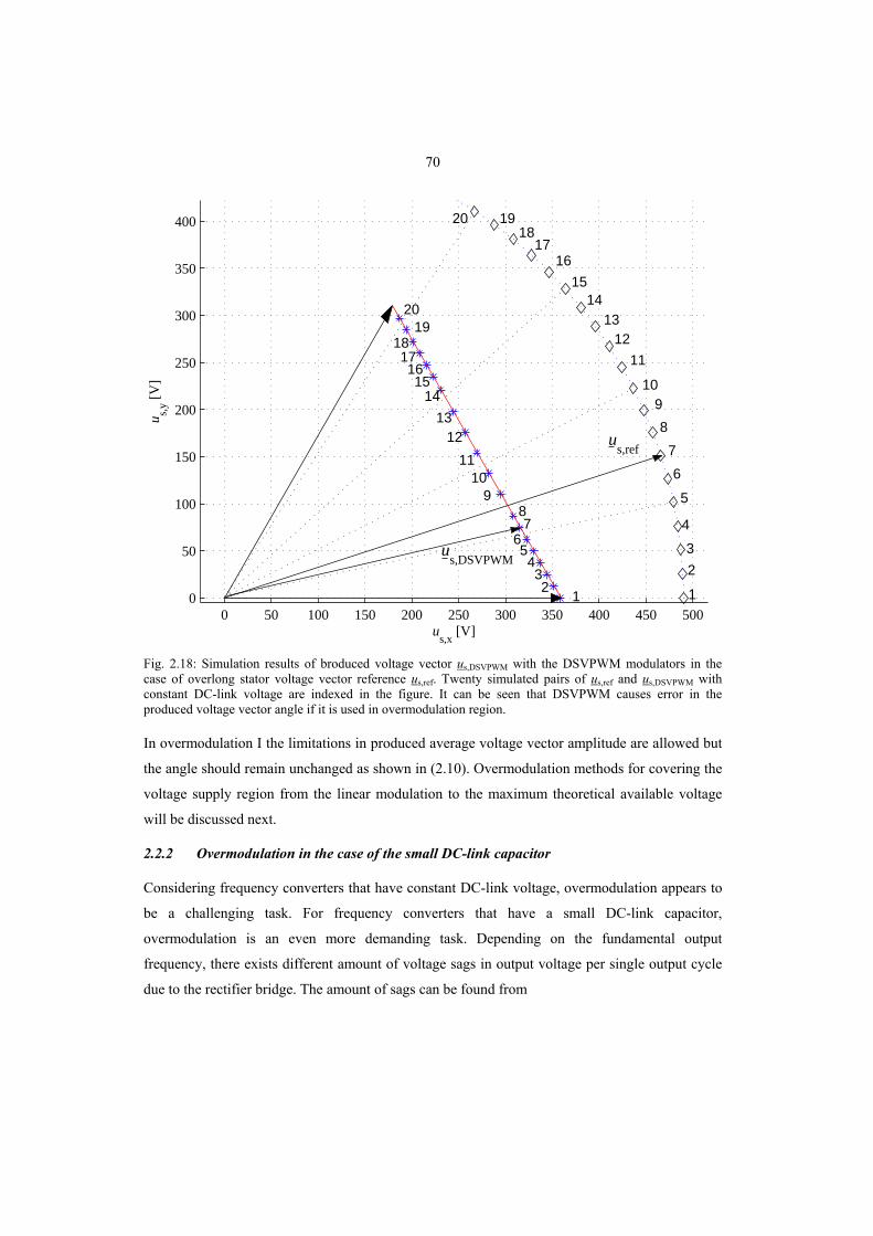
70
0 50 100 150 200 250 300 350 400 450 5000
50
100
150
200
250
300
350
400
us,x
[V]
u s,y [
V]
us,ref
us,DSVPWM
1 1
2 2
3
3 4
4
5
56
6
7
78
8
910
11
1213
1415
1617
181920
910
11
1213
1415
1617
1819
20
Fig. 2.18: Simulation results of broduced voltage vector us,DSVPWM with the DSVPWM modulators in the case of overlong stator voltage vector reference us,ref. Twenty simulated pairs of us,ref and us,DSVPWM with constant DC-link voltage are indexed in the figure. It can be seen that DSVPWM causes error in the produced voltage vector angle if it is used in overmodulation region.
In overmodulation I the limitations in produced average voltage vector amplitude are allowed but
the angle should remain unchanged as shown in (2.10). Overmodulation methods for covering the
voltage supply region from the linear modulation to the maximum theoretical available voltage
will be discussed next.
2.2.2 Overmodulation in the case of the small DC-link capacitor
Considering frequency converters that have constant DC-link voltage, overmodulation appears to
be a challenging task. For frequency converters that have a small DC-link capacitor,
overmodulation is an even more demanding task. Depending on the fundamental output
frequency, there exists different amount of voltage sags in output voltage per single output cycle
due to the rectifier bridge. The amount of sags can be found from

71
motor
grid6cycleoutput theof period one duringsagsvoltage
ff
= . (2.27)
Although the average value of the DC-link voltage is approximately equal to the version in
conventional size, the voltage drops need to be taken into account. Usually, DC-link voltage drops
due to the supply voltage failures are relatively slow. Now, as practically no energy storage exists,
the dynamic behavior of the DC-link is considerably faster compared with the traditionally
dimensioned frequency converter. Due to the voltage drops caused by the rectifier bridge, the
entry into the overmodulation region occurs earlier compared with the traditional frequency
converter.
Overmodulation I
The DC-link voltage waveforms used in the theoretical overmodulation calculations for
describing the VSI with small and big DC-link capacitor are shown in Fig. 2.19. The mean value
is used to describe the stiff DC-link voltage when a big DC-link capacitor is used. The theoretical
full-wave rectified voltage waveform is used to describe the DC-link voltage in the case of a small
DC-link capacitor. No feedforward from the modulator output to the DC-link voltage is included.
In reality, the modulator interacts with the DC-link voltage waveform and creates additional
distortion. This phenomenon is neglected in the following study for reasons of simplicity.
0 0.001 0.002 0.003 0.004 0.005 0.006 0.007 0.008 0.009 0.011.5
1.55
1.6
1.65
1.7
1.75
time [s]
u DC
[pu
]
mean value
Fig. 2.19: DC-link voltage waveforms used in the simulations. The ideal rectifier voltage is used as a DC-link voltage to model the DC-link without energy storage while the mean value of the ideal rectifier voltage is used as a stiff DC-link voltage.

72
The total harmonic distortion is used to illustrate the differences in output phase voltage
comparing the high-capacitance and small DC-link capacitor. The THD is defined as the RMS
value of the total harmonics of the signal, divided by the RMS value of its fundamental signal.
The voltage vector can be transformed in the phase voltages with (1.20). In the case of the U-
phase voltage, the THD is defined as
1U,
2
2U,
UTHDU
Un
ii∑
== , (2.28)
where U is the RMS value of the voltage. Subscript U defines the phase and i=2,3,…,n defines
the harmonic number. The fundamental value is identified with subscript 1.
The same overmodulation I methods discussed earlier can be utilized for overmodulation of the
small DC-link capacitor VSI. Under the overmodulation I mode the voltage amplitude is supposed
to track the fluctuating hexagon as shown in Fig. 2.11. Fig. 2.20 shows one electrical period of the
stator voltage reference vector us,ref, the maximum vector us,max and the actual modulated limited
vector path us,mod. The frequency of the stator voltage vector reference in the case described in the
figure is equal to the grid frequency. Due to the motor output frequency, 6 voltage drops are
taking place during one revolution of the voltage vector. Also the phase of the line voltage and the
motor voltage is chosen to be equal. Although this situation is possible, it is rare. However the
case is used because it points out the maximum fluctuation of the maximum available voltage
vector. The fluctuation is due to the combined dc-link and hexagon originated fluctuation. The
combined effect of the fluctuating DC-link voltage and the hexagon shaped maximum voltage
vector is represented in Fig. 2.21. The limits, which the combined effect of the hexagon and DC-
link fluctuation produces, are shown. Four different local minimum and maximum points can be
found. These are listed in Table 2.2. The absolute value depends on the line side properties that
affect the minimum and maximum absolute values of the DC-link voltage.

73
−1.5 −1 −0.5 0 0.5 1 1.5−1.5
−1
−0.5
0
0.5
1
1.5
us,x
[pu]
u s,y [
pu]
us,ref
us,max
us,mod
=min(us,max
, us,ref
)
Fig. 2.20: One electrical period of the stator voltage reference vector us,ref, the maximum vector us,max and the actual modulated limited vector path us,mod. Here, the frequency of the stator voltage vector reference is equal to the grid frequency. When the voltage is insufficient the modulator limits the voltage vector amplitude to the maximum voltage vector amplitude available.
Table 2.2: Four local extreme values of the stator voltage vector value
DCu Hexagon shape effect Combined effect
Min, ~1.5uB Min, 3/DCu ~0.866 uB
Max, ~1.73uB Min, 3/DCu ~1 uB
Min, ~1.5 uB Max, ( ) DC3/2 u ~1 uB
Max, ~1.73 uB Max, ( ) DC3/2 u ~1.153 uB

74
0 0.2 0.4 0.6 0.8 1 1.20
0.2
0.4
0.6
0.8
1
us,x
[pu]
u s,y [
pu]
2/3⋅1.73≈1.153
1/√(3)⋅1.5≈0.866
V1
V2 u
B=√(2/3)⋅400 V
Fig. 2.21: The combined effect of the DC-link voltage and hexagon shape on the instantaneous maximum available stator voltage vector trajectory. The limits set by the combined effect of the hexagon and the DC-link fluctuation produces are shown. Four different local minimum and maximum points can be found. When the minimum DC-link voltage level and the minimum hexagon radius are combined the maximum voltage radius is about 0.866 pu. When the maximum DC-link voltage level is combined with the minimum hexagon radius or the minimum DC-link voltage level with the maximum hexagon radius the output voltage radius is approximately 1 pu. When the maximum hexagon radius and the maximum DC-link voltage level are combined the output voltage vector in length of 1.153 pu is achieved.
Fluctuation due to the rectifier bridge occurs at a frequency of six times the line frequency, that is
grid6ω . The fundamental frequency of the motor refω and the DC-link fluctuation grid6ω form a
wobble phenomenon. This means that the instantaneous value of the fundamental voltage and its
harmonics are fluctuating. The symmetry of the hexagon shaped maximum voltage vector
trajectory creates a frequency which is six times the fundamental motor frequency. Because of the
wobble, the overmodulation fundamental voltage and its harmonic content needs to be studied
over the wobble period. Hence, the motor frequency is a parameter in the study. During the
wobble period the fluctuation of the DC-link voltage and the hexagon shaped maximum
instantaneous voltage together have combined all the amplitude limitation conditions in the
different voltage vector directions. The time period of wobbling twobble can be expressed as

75
refgridwobble 66
π2ωω −
=t . (2.29)
At certain motor frequencies the idea of the wobble period is insufficient for the purpose of
studying the variation levels of the total harmonic distortion (THD) and fundamental voltage.
These frequencies are 6,3,2,5.1,2.1,1ref =ω pu. These frequencies form a constant behavior
with the hexagon and DC-link waveform. At these frequencies, the THD and fundamental voltage
level in a certain phase are a function of the stator voltage vector initial angle versus the
instantaneous DC-link voltage level. The stator voltage vector initial angle θs,ref,0, that is the initial
phase of the output phase voltage, is included in the study as a parameter. The frequencies causing
constant behavior of the phase voltage are illustrated in Fig. 2.22.
0 1/3 2/3 1 4/3 5/3 21.5
1.55
1.6
1.65
1.7
1.75
θgrid= ωgridt [π ]
u DC [p
u]
ωref=1.2 ωgrid
ωref=1 ωgrid
ωref=1.5 ωgrid
ωref=2 ωgrid
ωref=3 ωgrid
ωref=6 ωgrid
Fig. 2.22: The frequencies causing constant behavior of the phase voltage waveform. The hexagon shape and DC-link voltage instantaneous levels form a time invariant phase voltage waveform with these angular frequency references.
The simulations have been used to carry out the theoretical study of the effect of the small DC-
link capacitor effect on the voltage supply of the VSI. The maximum and minimum THD level as
a function of the initial stator voltage vector angle θs,ref,0 and angular frequency reference ωref are
shown in Fig. 2.23. As the upper limit for the angular frequency reference, ωref =2.6 pu was
chosen to cover most of the mechanical applications.
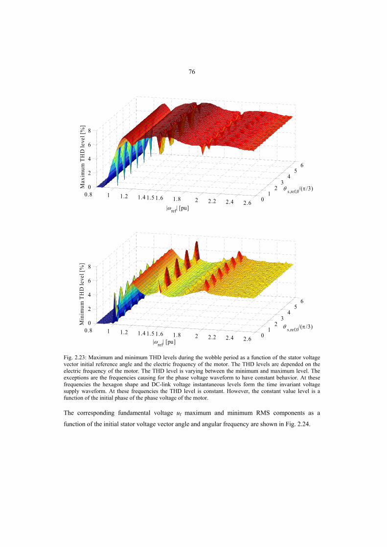
76
0.8 1 1.2 1.4 1.5 1.6 1.8 2 2.2 2.4 2.6 01
23
45
6
0
2
4
6
8
θ s ,ref,0/(π /3)
|ωref| [pu]
Max
imum
TH
D le
vel [
%]
0.8 1 1.2 1.4 1.5 1.6 1.8 2 2.2 2.4 2.6 01
23
45
6
0
2
4
6
8
Min
imum
TH
D le
vel [
%]
|ωref| [pu]
θ s ,ref,0/(π /3)
Fig. 2.23: Maximum and minimum THD levels during the wobble period as a function of the stator voltage vector initial reference angle and the electric frequency of the motor. The THD levels are depended on the electric frequency of the motor. The THD level is varying between the minimum and maximum level. The exceptions are the frequencies causing for the phase voltage waveform to have constant behavior. At these frequencies the hexagon shape and DC-link voltage instantaneous levels form the time invariant voltage supply waveform. At these frequencies the THD level is constant. However, the constant value level is a function of the initial phase of the phase voltage of the motor.
The corresponding fundamental voltage uf maximum and minimum RMS components as a
function of the initial stator voltage vector angle and angular frequency are shown in Fig. 2.24.
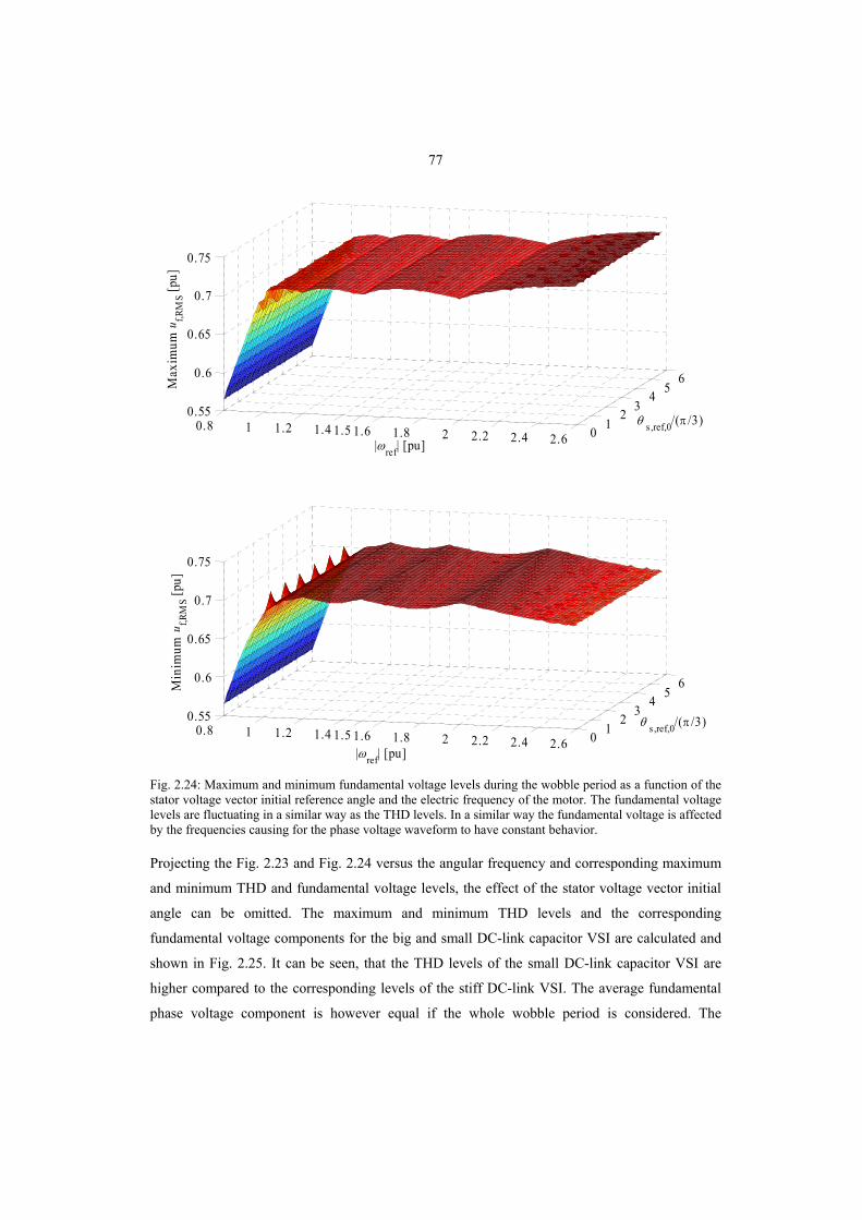
77
0.8 1 1.2 1.4 1.5 1.6 1.8 2 2.2 2.4 2.6 0 12 3
4 56
0.55
0.6
0.65
0.7
0.75
|ωref| [pu]
Max
imum
uf,R
MS [p
u]
0.8 1 1.2 1.4 1.5 1.6 1.8 2 2.2 2.4 2.6 0 12 3
4 56
0.55
0.6
0.65
0.7
0.75
Min
imum
uf,R
MS [p
u]
|ωref| [pu]
θ s ,ref,0/(π /3)
θ s ,ref,0/(π /3)
Fig. 2.24: Maximum and minimum fundamental voltage levels during the wobble period as a function of the stator voltage vector initial reference angle and the electric frequency of the motor. The fundamental voltage levels are fluctuating in a similar way as the THD levels. In a similar way the fundamental voltage is affected by the frequencies causing for the phase voltage waveform to have constant behavior.
Projecting the Fig. 2.23 and Fig. 2.24 versus the angular frequency and corresponding maximum
and minimum THD and fundamental voltage levels, the effect of the stator voltage vector initial
angle can be omitted. The maximum and minimum THD levels and the corresponding
fundamental voltage components for the big and small DC-link capacitor VSI are calculated and
shown in Fig. 2.25. It can be seen, that the THD levels of the small DC-link capacitor VSI are
higher compared to the corresponding levels of the stiff DC-link VSI. The average fundamental
phase voltage component is however equal if the whole wobble period is considered. The

78
theoretical modulation index M=0.952 is thus achieved in both cases. The effect of the wobbling
can be seen especially in the THD level variations.
0.866 1 1.2 1.4 1.6 1.8 2 2.2 2.40
0.02
0.04
0.06
0.08
Phas
e vol
tage
TH
D
min
imum
and
max
imum
[pu]
|ωref| [pu]
0.866 1 1.2 1.4 1.6 1.8 2 2.2 2.40.525
0.55
0.6
0.65
0.70710.725
0.75
Fund
amen
tal p
hase
vol
tage
RM
S va
lue u
f,RM
S [pu]
|ωref| [pu]
0.952⋅2/π ⋅1.65/√(2) = 0.7071
maximum peak T HD level with small dc-link capacitor VSI
minimum peak T HD level with small dc-link capacitor VSI
minimum peak T HD level with traditional-size dc-link capacitor VSI
maximum peak T HD level with traditional-size dc-link capacitor VSI
maximum peak funfamental voltage level with small dc-link capacitor VSI
minimum peak funfamental voltage level with small dc-link capacitor VSI
maximum and minimum peak funfamental voltage level with traditional-size dc-link capacitor VSI
Fig. 2.25: Projection of the THD and fundamental voltage waveforms in the direction of the initial stator voltage vector angle. The calculated maximum and minimum THD level and the corresponding fundamental voltage component during the wobble period for the big and small DC-link capacitor are shown. The THD level of the small DC-link capacitor VSI is higher compared to the stiff DC-link VSI. The average fundamental phase voltage component is nevertheless equal if the whole wobble period is considered.
Overmodulation II
The overmodulation II method described before is intended for constant DC-link voltage
applications. However it could also be used with the small DC-link capacitor VSI. The most
interesting alternative overmodulation method is presented by Bolognani et al. (1996). The
method is called Continuous Control. The idea is simply to track the angle that fulfills the stator
voltage vector reference amplitude. Under traditional overmodulation II, presented for example in
Holtz (1993), both the amplitude and angle of the stator voltage vector are controlled. Now, only
the angle is controlled. This results in simpler structure of the overmodulation control algorithms.
79
Bolognani et al. suggested that the Continuous Control can handle the whole region from the
beginning of the overmodulation I mode to the sixstep mode. There is, however, no reason why
the traditional overmodulation I mode could not be used first. On the contrary, by keeping the
angle of the stator voltage vector unchanged, as in OMI, the torque oscillation remains smaller
when compared to the Continuous Control. Torque oscillations are highly undesirable in many
cases. In this work, the Continuous Control is used after the overmodulation I mode has reached
the limit.
What makes this Continuous Control special in the case of a small DC-link capacitor is the inbuilt
ability of the method to track the stator voltage vector angle that fulfills the requested stator
voltage vector magnitude despite fluctuating DC-link voltage. Even Bolognani et al. do not
discuss the ability of the method to respond to the change in DC-link voltage, this property can be
seen from the equations. Since the method is used after the overmodulation I and because of its
ability to track the angle fulfilling the voltage amplitude, the method is here renamed Constant
Amplitude (CA) overmodulation. The Constant Amplitude is chosen to be used as the OM II
method in this work.
The closest vector that satisfies the magnitude reference refs,u can be found from the angle CVθ ,
which is defined from the middle of the sector and can be found from
⎟⎟
⎠
⎞
⎜⎜
⎝
⎛= −
refs,
DC31
1CV cos
u
uθ . (2.30)
The values of the angle CVθ are limited to [0… 6π ]. Hence, the case of CVθ = 6π corresponds
to the sixstep operation mode and CVθ =0 suggests that the stator voltage reference is achievable
without any change in the angle. When CVθ =0, the stator voltage vector is in linear modulation
region. This is illustrated in Fig. 2.26. The linear modulation region is achievable in the hatched
area. Depending on the stator voltage reference vector angle ( ) refs,refs,arg θ=u , the term CVθ is
added to or subtracted from the final angle of the constant amplitude vector as

80
( )
( )
( )
( )3π1
6π
6π
3π1
3π1
6π
6π
3π1
CVCA
refs,
CVCA
refs,
m-
m-
m-
m-
++=⇒
+>
+−=⇒
+≤
θθ
θ
θθ
θ
. (2.31)
The original stator voltage reference vector (1.6) is then replaced by
CAjrefs,CAref,s, e θuu = . (2.32)
The subscript CA stands for Constant Amplitude and describes the ability of the method to
maintain the amplitude reference unchanged. The angle CAθ represents the angle where the stator
voltage amplitude fulfils the reference amplitude.
refs,u
CVθ
CVθ CAθ
m=1952.0>M
DC32V u=
2V
1V
Fig. 2.26: The Constant Amplitude overmodulation tracks the closest stator voltage vector that fulfills the magnitude of the reference stator voltage vector. In the case of a constant DC-link voltage level the reference stator voltage vector angle is limited to the closest angle where the amplitude of the voltage vector reference is located. The red line represents the reference voltage vector us,ref. The green line represents the voltage vector reference limited by the CA overmodulation us,ref,CA. The hatched area represents the angle references allowed by the CA overmodulation. The discontinuity between the hatched areas represents the stator voltage vector angle references that, in this case, do not fulfill the voltage vector amplitude reference.
To illustrate the functionality of the presented CA overmodulation method, two figures of the
sector m=1 are shown. In both of the figures the DC-link voltage is decreasing. Under the DC-link
voltage level variations the angle is varied according to (2.30). In Fig. 2.27 the stator voltage
vector angle reference is located in the first half of the sector, that is ( )6π
3π1refs, +≤ m-θ . Under
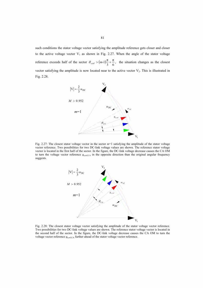
81
such conditions the stator voltage vector satisfying the amplitude reference gets closer and closer
to the active voltage vector V1 as shown in Fig. 2.27. When the angle of the stator voltage
reference exceeds half of the sector ( )6π
3π1refs, +> m-θ , the situation changes as the closest
vector satisfying the amplitude is now located near to the active vector V2. This is illustrated in
Fig. 2.28.
m=1
DC32V u=
952.0>M
DCurefω
1V
2V
CVθ
refs,u
Fig. 2.27: The closest stator voltage vector in the sector m=1 satisfying the amplitude of the stator voltage vector reference. Two possibilities for two DC-link voltage values are shown. The reference stator voltage vector is located in the first half of the sector. In the figure, the DC-link voltage decrease causes the CA OM to turn the voltage vector reference us,ref,CA in the opposite direction than the original angular frequency suggests.
m=1
DC32V u=
952.0>M
DCu
refω
1V
2V
CVθ
refs,u
Fig. 2.28: The closest stator voltage vector satisfying the amplitude of the stator voltage vector reference. Two possibilities for two DC-link voltage values are shown. The reference stator voltage vector is located in the second half of the sector. In the figure, the DC-link voltage decrease causes the CA OM to turn the voltage vector reference us,ref,CA further ahead of the stator voltage vector reference.

82
The constant amplitude fundamental voltage output CAf,u can be found from
( ) ⎟⎟⎠
⎞⎜⎜⎝
⎛⎟⎠⎞
⎜⎝⎛ −+= ggrefs,refs,CAf, 6πsin
π6 ααuuu , (2.33)
where
( )
32
3
3cos6π
DCrefs,
DC
refs,
DC
1refs,g
uuu
u
u
u
≤≤
⎟⎟⎟⎟
⎠
⎞
⎜⎜⎜⎜
⎝
⎛
−= −α. [2.12]
A more precise mathematical formation of the fundamental output voltage equation can be found
from Bolognani et al. (1996).
Example measurement of the Constant Amplitude overmodulation
The measured supply grid line current waveform and the FFT calculated under CA OM are shown
in Fig. 2.29. As it can be seen, the line current has considerable distortion. However, the
frequency content of the supply grid current, shown in the FFT graph, is still better than in the
normal case of high-capacitance VSI shown in figs Fig. 1.10 and Fig. 2.10. The VSI with small
DC-link capacitor generates smaller 5th and the 7th harmonic components even though the line
current is strongly distorted because of the CA overmodulation. Fig. 2.30 shows the behavior of
the angle limited by the CA OM algorithm during a single stator voltage vector revolution. The
electric frequency is 80 Hz (1.6 pu).

83
0 0.005 0.01 0.015 0.02 0.025 0.03 0.035 0.04
−10
−5
0
5
10
time [s]
Supp
ly g
rid
curr
ent [
A]
50 110 250 350 430 530 800 10000
1
2
3
4
5
frequency [Hz]
FFT
of
supp
ly g
rid
curr
ent [
A]
Fig. 2.29: Measured waveform of the supply grid line current and calculated FFT. The line current waveform, having considerable distortion, has still satisfactory frequency content.
0 0.002 0.004 0.006 0.008 0.01 0.012-4
-3
-2
-1
0
1
2
3
4
time [s]
Stat
or v
olta
ge v
ecto
r ang
le re
fere
nce [
π ]
θs,ref θCA
2π /ωref=0.0125s
Fig. 2.30: Recorded behavior of the stator voltage angle reference θs,ref and the CA limited angle θCA during one stator voltage vector revolution. The stator voltage vector angle reference is controlled by the constant amplitude overmodulation method such that it turns into the closest direction fulfilling the amplitude reference.

84
Fig. 2.31 describes the realized voltage vector values - fulfilling the stator voltage amplitude
reference - that are obtained under CA OM during a single revolution of the stator reference
voltage vector. Only directions fulfilling the amplitude reference are used. The maximum
instantaneous voltage vector trajectory in the direction of the stator voltage vector reference is
also shown. For low voltage values, the active voltage vector directions are used. In cases when
the DC-link voltage is high and the limit of the linear modulation voltage vector reference is
exceeded, the linear modulation is used. The different stator voltage vector references of the OM I
and the CA OM are due to the aim to supply equal fundamental voltage with different modulation
methods. The direction of the realized CA OM voltage vector is alternating rapidly due to the
heavily fluctuating DC-link voltage shown in Fig. 2.32.
−1.5 −1 −0.5 0 0.5 1 1.5−1.5
−1
−0.5
0
0.5
1
1.5
x [pu]
y [p
u]
us,ref
for CA CA realized stator voltage vector
under high voltage situation linear modulation was used
us,ref
for linear modulation
and OM I
uB=√(2/3)⋅400 V
Maximum available stator voltage vector in the direction of u
s,ref
Fig. 2.31: Measurement values for the recorded voltage vector references under linear modulation and under CA OM. us,ref is for the linear modulation. In two cases the DC-link voltage spikes reach so high that the linear modulation is used. Otherwise, CA OM is used. In the case of the low DC-link voltage, the voltage vector in the direction of the active voltage vector is chosen by the CA OM. This operation mode corresponds to the sixstep operation.

85
A lot of distortion in the DC-link voltage exists. Due to the extremely strong interaction between
the modulator and the DC-link voltage waveform, no simplified DC-link voltage waveform
approximation was found. Thus, the fundamental component of the output voltage and its THD
level fluctuations are not possible to calculate in the same way as in the case of overmodulation I.
The MPPF type capacitor can cope with the heavily fluctuating voltage without premature
deterioration.
0 0.002 0.004 0.006 0.008 0.01 0.012350
400
450
500
550
600
650
700
750
time [s]
DC-
link
volta
ge [p
u]
2π/ω ref=0.0125s
Fig. 2.32: Measured DC-link voltage during one stator voltage vector reference revolution. The DC-link voltage is heavily distorted. However, the MPPF type capacitors can take up to 1200 V DC-link voltage. The level is therefore no problem as service life-time is considered.
The researcher familiar with field-oriented control may find it more familiar to study the
phenomena of motor control through the produced stator flux linkage s
ψ . The produced stator
flux linkage can be roughly estimated by integrating the recorded stator voltage vector references
realized by the Constant Amplitude overmodulation us,CA. In Fig. 2.33 one revolution of the
realized stator voltage vector trajectory and the estimated stator flux linkage are shown. The flux
linkage path forms almost a hexagon.
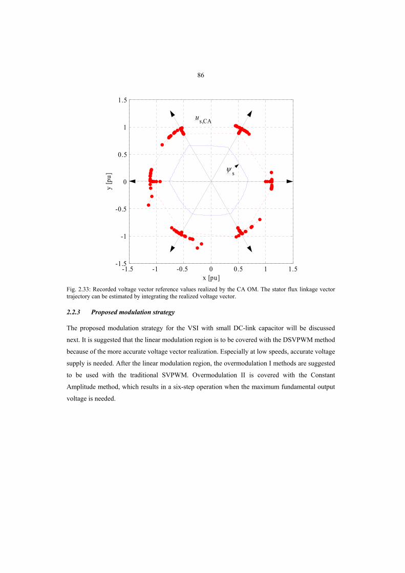
86
-1.5 -1 -0.5 0 0.5 1 1.5-1.5
-1
-0.5
0
0.5
1
1.5
x [pu]
y [p
u]us,CA
ψ s
Fig. 2.33: Recorded voltage vector reference values realized by the CA OM. The stator flux linkage vector trajectory can be estimated by integrating the realized voltage vector.
2.2.3 Proposed modulation strategy
The proposed modulation strategy for the VSI with small DC-link capacitor will be discussed
next. It is suggested that the linear modulation region is to be covered with the DSVPWM method
because of the more accurate voltage vector realization. Especially at low speeds, accurate voltage
supply is needed. After the linear modulation region, the overmodulation I methods are suggested
to be used with the traditional SVPWM. Overmodulation II is covered with the Constant
Amplitude method, which results in a six-step operation when the maximum fundamental output
voltage is needed.
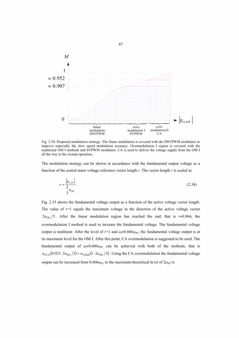
87
907.0952.0
1
≈≈
0 refs,u
M
43421
CAII modulation
-over43421
SVPWMI modulation
-over4444 34444 21
DSVPWMmodulation
linear
Fig. 2.34: Proposed modulation strategy. The linear modulation is covered with the DSVPWM modulator to improve especially the slow speed modulation accuracy. Overmodulation I region is covered with the traditional OM I methods and SVPWM modulator. CA is used to deliver the voltage supply from the OM I all the way to the sixstep operation.
The modulation strategy can be shown in accordance with the fundamental output voltage as a
function of the scaled stator voltage reference vector length r. The vector length r is scaled as
DC
refs,
32 u
ur = . (2.34)
Fig. 2.35 shows the fundamental voltage output as a function of the active voltage vector length.
The value of r=1 equals the maximum voltage in the direction of the active voltage vector
32 DCu . After the linear modulation region has reached the end, that is r≈0.866, the
overmodulation I method is used to increase the fundamental voltage. The fundamental voltage
output is nonlinear. After the level of r=1 and uf≈0.606uDC, the fundamental voltage output is at
its maximum level for the OM I. After this point, CA overmodulation is suggested to be used. The
fundamental output of uf≈0.606uDC can be achieved with both of the methods, that is
( ) ( )32132921.0 DCf,OMIDCf,CA uuuu ⋅=⋅ . Using the CA overmodulation the fundamental voltage
output can be increased from 0.606uDC to the maximum theoretical level of 2uDC/π.

88
0.560
0.570
0.580
0.590
0.600
0.610
0.620
0.630
0.840 0.860 0.880 0.900 0.920 0.940 0.960 0.980 1.000
r [pu]
Overmodulation IConstant AmplitudeLinear modulation
2/π
change between modulation
i i l OM I d CA
DC
fu
u
866.023
≈=r
Fig. 2.35: Fundamental voltage supply under proposed overmodulation combination. After the linear modulation region has reached the end, that is r≈0.866, the overmodulation I method is used to increase the fundamental voltage. The fundamental voltage output is strongly nonlinear. After the level of r=1 and uf≈0.606uDC, the fundamental voltage output is at its maximum level with OM I. After this point, CA overmodulation is used. The fundamental output of uf≈0.606uDC can be achieved with both of the method, that is uf,CA(0.921⋅2uDC/3)=uf,OMI(1⋅2uDC/3). In using the CA overmodulation the fundamental voltage output can be increased from 0.606uDC to the maximum theoretical level of 2uDC/π.
2.3 Overvoltage protection
In this section a simple overvoltage protection method is explained and verified. The method is
based on the control of the angle between the stator voltage and the current vectors. The cosine of
this angle is commonly known as the power factor. The motor is braking when the direction of
power flow changes from the motor towards the converter. In advanced frequency converter
control systems braking may be easily prevented. In methods like current vector control and DTC,
the electric torque te can be calculated and controlled through estimated fluxes (rotor or stator). As
an example, the DTC torque calculation is formed by Takahashi et al. (1986) as
( )
sse
ssss
23
d
iψpt
tiRuψ
×=
−= ∫, (2.35)
where us, is and Rs are the stator voltage vector, current vector and resistance respectively. Motor
pole pair is denoted with p.
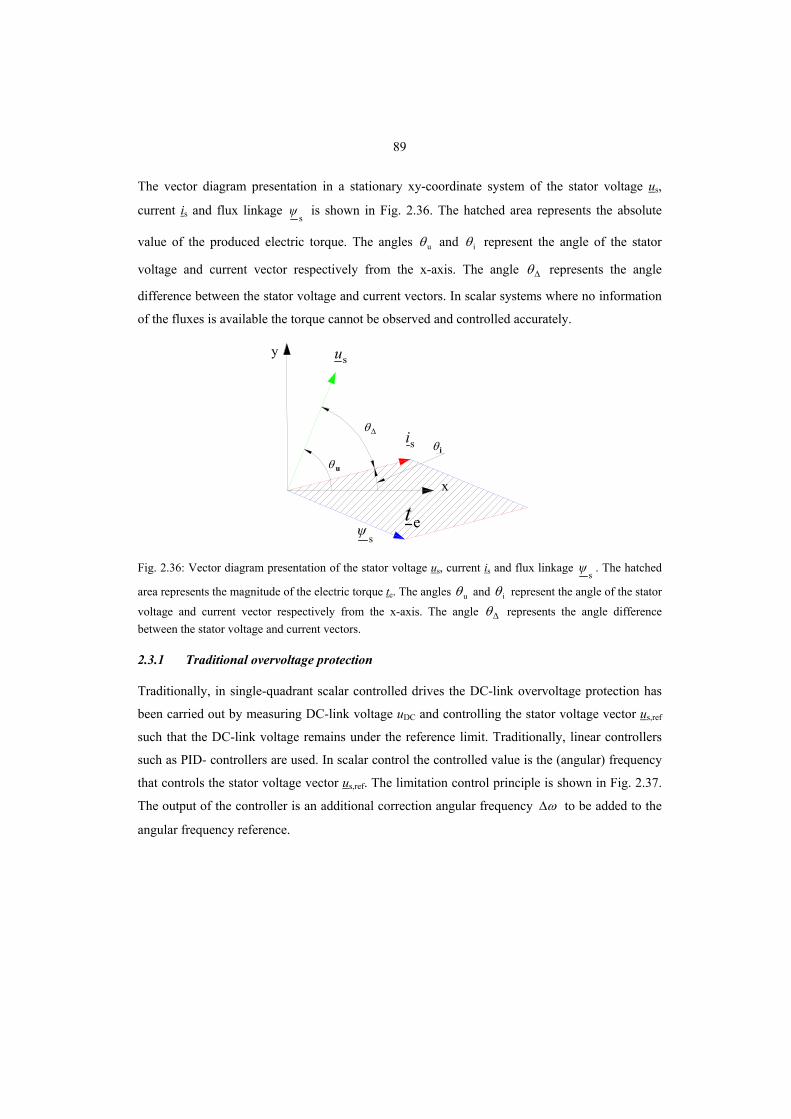
89
The vector diagram presentation in a stationary xy-coordinate system of the stator voltage us,
current is and flux linkage s
ψ is shown in Fig. 2.36. The hatched area represents the absolute
value of the produced electric torque. The angles uθ and iθ represent the angle of the stator
voltage and current vector respectively from the x-axis. The angle ∆θ represents the angle
difference between the stator voltage and current vectors. In scalar systems where no information
of the fluxes is available the torque cannot be observed and controlled accurately.
si
x
su
iθ∆θ
uθ
et
y
sψ
Fig. 2.36: Vector diagram presentation of the stator voltage us, current is and flux linkage
sψ . The hatched
area represents the magnitude of the electric torque te. The angles uθ and iθ represent the angle of the stator
voltage and current vector respectively from the x-axis. The angle ∆θ represents the angle difference between the stator voltage and current vectors.
2.3.1 Traditional overvoltage protection
Traditionally, in single-quadrant scalar controlled drives the DC-link overvoltage protection has
been carried out by measuring DC-link voltage uDC and controlling the stator voltage vector us,ref
such that the DC-link voltage remains under the reference limit. Traditionally, linear controllers
such as PID- controllers are used. In scalar control the controlled value is the (angular) frequency
that controls the stator voltage vector us,ref. The limitation control principle is shown in Fig. 2.37.
The output of the controller is an additional correction angular frequency ω∆ to be added to the
angular frequency reference.
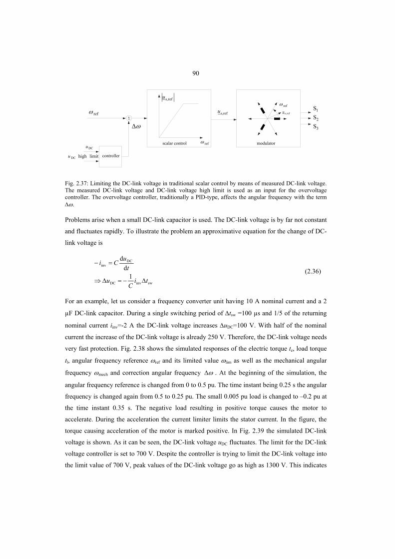
90
refω
refω
controller
ω∆
DCumodulatorscalar control
∑
refω
3
2
1
SSS
limithighDCu
refs,u
refs,u refs,u
Fig. 2.37: Limiting the DC-link voltage in traditional scalar control by means of measured DC-link voltage. The measured DC-link voltage and DC-link voltage high limit is used as an input for the overvoltage controller. The overvoltage controller, traditionally a PID-type, affects the angular frequency with the term ∆ω.
Problems arise when a small DC-link capacitor is used. The DC-link voltage is by far not constant
and fluctuates rapidly. To illustrate the problem an approximative equation for the change of DC-
link voltage is
swinvDC
DCinv
1d
d
tiC
u
tuCi
∆−=∆⇒
=− (2.36)
For an example, let us consider a frequency converter unit having 10 A nominal current and a 2
µF DC-link capacitor. During a single switching period of ∆tsw =100 µs and 1/5 of the returning
nominal current iinv=-2 A the DC-link voltage increases ∆uDC=100 V. With half of the nominal
current the increase of the DC-link voltage is already 250 V. Therefore, the DC-link voltage needs
very fast protection. Fig. 2.38 shows the simulated responses of the electric torque te, load torque
tl, angular frequency reference ωref and its limited value ωlim as well as the mechanical angular
frequency ωmech and correction angular frequency ω∆ . At the beginning of the simulation, the
angular frequency reference is changed from 0 to 0.5 pu. The time instant being 0.25 s the angular
frequency is changed again from 0.5 to 0.25 pu. The small 0.005 pu load is changed to –0.2 pu at
the time instant 0.35 s. The negative load resulting in positive torque causes the motor to
accelerate. During the acceleration the current limiter limits the stator current. In the figure, the
torque causing acceleration of the motor is marked positive. In Fig. 2.39 the simulated DC-link
voltage is shown. As it can be seen, the DC-link voltage uDC fluctuates. The limit for the DC-link
voltage controller is set to 700 V. Despite the controller is trying to limit the DC-link voltage into
the limit value of 700 V, peak values of the DC-link voltage go as high as 1300 V. This indicates
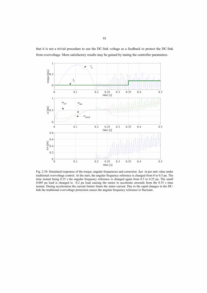
91
that it is not a trivial procedure to use the DC-link voltage as a feedback to protect the DC-link
from overvoltage. More satisfactory results may be gained by tuning the controller parameters.
0 0.1 0.2 0.25 0.3 0.35 0.4 0.5
0
0.5
1
torq
ue [p
u]
time [s]
0 0.1 0.2 0.25 0.3 0.35 0.4 0.50
0.5
1
time [s]
ω [p
u]
0 0.1 0.2 0.25 0.3 0.35 0.4 0.50
0.2
0.4
0.6
0.8
∆ω
[pu]
time [s]
te
ωref ωlim
ωmech
tl
Fig. 2.38: Simulated responses of the torque, angular frequencies and correction ω∆ in per unit value under traditional overvoltage control. At the start, the angular frequency reference is changed from 0 to 0.5 pu. The time instant being 0.25 s the angular frequency reference is changed again from 0.5 to 0.25 pu. The small 0.005 pu load is changed to –0.2 pu load causing the motor to accelerate onwards from the 0.35 s time instant. During acceleration the current limiter limits the stator current. Due to the rapid changes in the DC-link the traditional overvoltage protection causes the angular frequency reference to fluctuate.

92
0 0.1 0.2 0.25 0.3 0.35 0.4 0.50
200
400
600
800
1000
1200
u DC
[V
]
time [s] Fig. 2.39: Simulated DC-link voltage under traditional overvoltage control. A change in angular frequency reference from 0 to 0.5 pu was made at the beginning. The time instant being 0.25 s the angular frequency reference is changed again from 0.5 to 0.25 pu. Small load 0.005 pu was changed to –0.2 pu load at the time instant 0.35 s. The DC-link voltage gets extremely high.
In Fig. 2.40 the angle between stator voltage and current is observed during the same frequency
step. During acceleration, the power flows from the inverter to motor. This can be observed from
the angle. At the moment when the torque tends to get negative, the fast dynamic of the small DC-
link capacitor is observed. The angle ∆θ between stator voltage and current varies heavily when
electric torque te is close to zero-torque. This is because of the PID controller which reacts to the
rapidly changing DC-link voltage every time the level of 700 V is exceeded.

93
0 0.1 0.2 0.25 0.3 0.35 0.4 0.5-0.3
-0.2
-0.1
0
0.1
0.2
0.3
0.40.45
0.5
0.6
0.7
θ ∆ [π
]
time [s]
Fig. 2.40: The angle ∆θ between the stator voltage and current vectors during frequency step simulation under traditional overvoltage control.
2.3.2 Dynamic Power Factor Control (DPFC) for overvoltage protection
Because of the fast dynamics of the DC-link voltage a different aspect has to be adopted in the
overvoltage protection. The ideal situation would be if the controller could identify the braking
situation before it occurs. A new method named Dynamic power factor control (DPFC) is
introduced and verified to fulfill the demand of overvoltage protection of the small DC-link
capacitor VSI. The DPFC is intended to be used especially in scalar controlled electric drives
where no torque estimation exists. The DPFC method is based on the control of the power factor,
that is the cosine of the angle ∆θ locating between the stator voltage vector us and the current
vector is. The mathematical methods for finding the angle ∆θ can vary. One possible way is to
align the d-axis of the synchronous rotating dq-reference frame with the stator current vector. The
vector diagram is shown in Fig. 2.41.

94
si
x
su
sψ
d
iθ
∆θ
uθ
q y
Fig. 2.41: Coordinate system and vector diagram of the stator voltage us, flux linkage ψs and current is. The synchronous dq-reference frame is aligned with the stator current vector.
The stator voltage reference vector us,ref is transformed into the dq-frame by using equation
( ) ( )( ) ( ) ⎥
⎦
⎤⎢⎣
⎡⎥⎦
⎤⎢⎣
⎡−
=⎥⎦
⎤⎢⎣
⎡
yref,s,
xref,s,
qs,
ds,
cossinsincos
uu
uu
ii
ii
θθθθ
. (2.37)
The angle between the stator voltage and current vectors can now be calculated from
⎟⎟⎠
⎞⎜⎜⎝
⎛= −
∆s,d
s,q1tanuu
θ . (2.38)
The angle iu θθθ −=∆ between the stator voltage and current vectors works as an input for the
controller. Despite the heavily fluctuating DC-link voltage, the angle ∆θ remains relatively calm
in every situation.
Zero-torque is obtained in the instance in which the flux linkage vector s
ψ and stator current
vector is are overlapping. The power starts to flow from the motor to the DC-link at the moment
when the negative angle between flux linkage and current vector is created. During zero-torque
the induction motor rotor rotates in synchronous angular frequency with the stator voltage vector.
This leads to a zero-rotor current. The induction motor stator voltage space vector presentation,
shown e.g. in Leonhard (1996), may thus be simplified during zero-torque as
s
ssss jψ
ω iLiRu s += , (2.39)
where the Ls is the stator inductance.
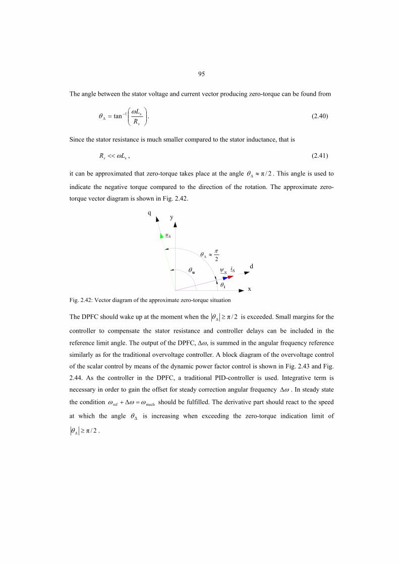
95
The angle between the stator voltage and current vector producing zero-torque can be found from
⎟⎟⎠
⎞⎜⎜⎝
⎛= −
sRLs1
∆ tanω
θ . (2.40)
Since the stator resistance is much smaller compared to the stator inductance, that is
sLRs ω<< , (2.41)
it can be approximated that zero-torque takes place at the angle 2/π≈∆θ . This angle is used to
indicate the negative torque compared to the direction of the rotation. The approximate zero-
torque vector diagram is shown in Fig. 2.42.
qy
x
d
Su
uθ
iθ
2∆πθ ≈
SiSψ
Fig. 2.42: Vector diagram of the approximate zero-torque situation
The DPFC should wake up at the moment when the 2/π≥∆θ is exceeded. Small margins for the
controller to compensate the stator resistance and controller delays can be included in the
reference limit angle. The output of the DPFC, ∆ω, is summed in the angular frequency reference
similarly as for the traditional overvoltage controller. A block diagram of the overvoltage control
of the scalar control by means of the dynamic power factor control is shown in Fig. 2.43 and Fig.
2.44. As the controller in the DPFC, a traditional PID-controller is used. Integrative term is
necessary in order to gain the offset for steady correction angular frequency ω∆ . In steady state
the condition mechref ωωω =∆+ should be fulfilled. The derivative part should react to the speed
at which the angle ∆θ is increasing when exceeding the zero-torque indication limit of
2/π≥∆θ .

96
scalar control modulator
refω
ω∆∑
refω
refωq y
x
d
iθ
uθ
∆θ
DPFC
3
2
1
SSS
si
refs,u
refs,u
si
refs,u
refs,urefs,u
Fig. 2.43: Block diagram of the overvoltage control of the scalar control by means of the dynamic power factor control. The power factor controller needs the stator current and voltage vectors as inputs. The output can be added to the angular frequency reference.
ω∆
si iθ
∆θ
DPFC
refs,ucontroller
( )
⎟⎟⎠
⎞⎜⎜⎝
⎛=
=⎥⎦
⎤⎢⎣
⎡
−∆
s,d
s,q1
irefs,s,q
s,d
tan
,f
uu
uuu
θ
θ
⎟⎟⎠
⎞⎜⎜⎝
⎛−
xs,
ys,1tanii
Fig. 2.44: Block diagram of the dynamic power factor control unit. The angle between the stator current vector and stator voltage vector θ∆ is used as an input for the controller. As the controller a traditional PID controller can be used. The controller produces the overvoltage protection control signal ∆ω to be summed in the angular frequency reference.
The same simulation sequence as used for the traditional overvoltage control has been used here
to verify the new DPFC system. The simulated responses of the electric torque te and the load
torque tl, angular frequency reference ωref and its limited value ωlim as well as the mechanical
angular frequency ωmech and correction angular frequency ω∆ during operation of the DPFC
controller are shown in Fig. 2.45. The DPFC becomes active when the torque tends to get
negative at the instant 0.2 s. In Fig. 2.46 the DC-link voltage during operation of the DPFC is
shown. No overvoltage situation occurs.

97
0 0.1 0.2 0.25 0.3 0.35 0.4 0.50
0.2
0.5
1to
rque
[pu]
time [s]
0 0.1 0.2 0.25 0.3 0.35 0.4 0.50
0.2
0.4
0.6
0.8
ω [p
u]
time [s]
0 0.1 0.2 0.25 0.3 0.35 0.4 0.50
0.1
0.2
0.3
0.4
0.5
∆ω
[pu]
time [s]
te
tl
ωref ωlim
ωmech
Fig. 2.45: Simulated responses of torque, angular frequencies and correction term ∆ω in per unit value under DPFC. The same sequence for this case is used as in the previous case.
0 0.1 0.2 0.25 0.3 0.35 0.4 0.50
100
200
300
400
500
600
u DC
[V
]
time [s] Fig. 2.46: Simulated DC-link voltage under DPFC. No high voltage peaks occur.

98
In Fig. 2.47 the angle ∆θ is shown during a step change of the reference frequency. The angle is
controlled such that the reference limit to the angle π45.02/π90% =⋅=∆θ is the upper limit.
The value 90% gives a small margin for the controller and includes a small effect of the stator
resistance shown in (2.40). This angle limit reference may result in a very small positive torque.
Comparison to the case illustrated in Fig. 2.40, where traditional overvoltage control is used, the
difference is clear. No fluctuation in the angle exists when the operating mode of the motor is
close to zero-torque. The result is a more fluent behavior of the motor during retardation.
0 0.1 0.2 0.25 0.3 0.35 0.4 0.5-0.3
-0.2
-0.1
0
0.1
0.2
0.3
0.40.45
0.5
time [s]
θ ∆ [π
]
Fig. 2.47: The angle θ∆ between stator voltage and current during the frequency step during operation of the
DPFC.
Verification has been done also with the experimental device. A measurement example of the
DPFC is shown in Fig. 2.48. The load machine is controlled to rotate at a constant 0.3 pu angular
frequency. The load motor nominal torque is much higher compared to the controlled test motor.
The test motor was used with an angular speed reference sequence ωref=0.24, 0.32, 0.24 pu.
With the experimental device the angle limit reference is controlled up to the upper limit of
π45.02/π90% =⋅=∆θ . As can be seen, the DC-link can be protected by using DPFC. When
the angular frequency reference is smaller than the load speed the DPFC controls the difference
between load and test motor to be set equal. Thus the correction becomes ∆ω =(0.3-0.24)pu=0.06
pu.

99
0 4 5 10 13.5 15 200
0.060.1
0.240.32
0.4
0.5A
ngul
ar fr
eque
ncy
[pu]
time [s]
0 4 5 10 13.5 15 20450
500
550
600
DC-
link
volta
ge [V
]
time [s]
0 4 5 10 13.5 15 200.1
0.2
0.3
0.40.45
0.5
θ∆
[π]
time [s]
ω ref
∆ω
Fig. 2.48: The measured angular frequency reference ωref and correction ∆ω , DC-link voltage and the angle θ∆ between stator voltage and current during the angular frequency sequence with the DPFC.
The DPFC is a very simple method for dealing with the problem of the overvoltage control. No
additional measurements are needed. Only information from the reference stator voltage vector
and measured stator currents are required.
2.4 Resonance between line inductor and DC-link capacitor
Due to the small DC-link capacitor the resonance frequency between the DC-link capacitance and
line side inductance becomes significantly high. The resonance frequency can get close to or even
exceed the switching frequency. In Phipps (1997) a transfer function approach is used to study the

100
harmonic filter design. Here, the method is used to study the interactions between the supply grid
and the DC-link. The supply grid is modeled as the Thevenin equivalent impedance Zgrid. The line
side AC-inductor LAC can be included in the supply grid impedance. The DC-link capacitor can be
modeled as the impedance and referred to as a filter and denoted as Zfil. This is illustrated in the
Fig. 2.49. The harmonic source for the grid/filter impedance Hgf system can be either the rectifier
bridge Urec or the inverter bridge Uinv voltage or both of them.
gridZ
filZrecU invU
gridI I
filI
Fig. 2.49: Representation of the line impedance and DC-link impedance connection. The rectifier bridge or inverter bridge is considered to be the input stimulus for the impedance system. Zgrid is used to describe the combined supply grid and AC-filter impedance. The DC-link impedance is modeled with Zf.
The grid/filter impedance transfer function presentation in Laplace’s s-domain is
( ) ( )
( ) ( )( ) ( ) ,
filgrid
filgrid
filgridgf
sZsZsZsZ
IIsU
sH
+=
+=
(2.42)
where U is either the rectifier bridge Urec or the inverter bridge Uinv voltage.
Assuming that the supply grid combined with the AC-inductor impedance includes an inductive
and resistive part, the equation for Zgrid becomes
( ) gridgridgrid sLRsZ += . (2.43)
The DC-link inductor can be assumed to be a pure capacitor. The equation for Zfil is then
( )sC
sZ 1fil = . (2.44)
By substituting (2.43) and (2.44) into (2.42) the grid/filter impedance equation becomes

101
( )1grid
2grid
gridgridgf ++
+=
CsRCsLsLR
sH . (2.45)
Further substitution of s=jω in (2.45) yields the grid/filter impedance equation in the frequency
domain. By solving the angular frequency when the real part of the denominator becomes zero,
the resonance frequency ωres is obtained. The resonance angular frequency is
CLgridres
1=ω . (2.46)
The ratio of the supply grid current and the injected current is defined as Hc2g
( )
( )( )
11
grid2
grid
grid
gf
filgrid
gridc2g
++=
=
+=
CsRCsL
sZsH
III
sH
. (2.47)
This is an important result since it presents the ratio of the supply grid current and the harmonic
current injected by the harmonic voltage source. The magnitude of the grid/filter impedance and
the magnitude of the supply grid current as a function of the injected current frequency in the
frequency domain are shown in Fig. 2.50. It can be shown that the resonance peak amplitude gain
Gg is
( )
CL
R
HG
grid
grid
resc2gg
1
j
=
= ω
. (2.48)
This gain is widely known as filter quality factor. If the harmonic voltage source injects harmonic
current components close to the resonance frequency, the supply grid current includes a high
amount of resonance frequency current components.
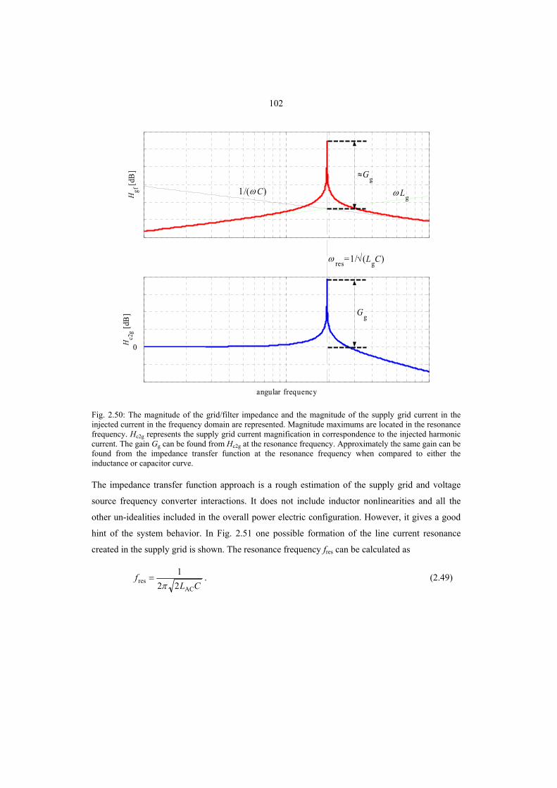
102
Hgf
[dB
]
0
angular frequency
Hc2
g [dB
]
ω res=1/√(LgC)
ω Lg 1/(ω C)
≈Gg
Gg
Fig. 2.50: The magnitude of the grid/filter impedance and the magnitude of the supply grid current in the injected current in the frequency domain are represented. Magnitude maximums are located in the resonance frequency. Hc2g represents the supply grid current magnification in correspondence to the injected harmonic current. The gain Gg can be found from Hc2g at the resonance frequency. Approximately the same gain can be found from the impedance transfer function at the resonance frequency when compared to either the inductance or capacitor curve.
The impedance transfer function approach is a rough estimation of the supply grid and voltage
source frequency converter interactions. It does not include inductor nonlinearities and all the
other un-idealities included in the overall power electric configuration. However, it gives a good
hint of the system behavior. In Fig. 2.51 one possible formation of the line current resonance
created in the supply grid is shown. The resonance frequency fres can be calculated as
CLf
ACres 22
1π
= . (2.49)
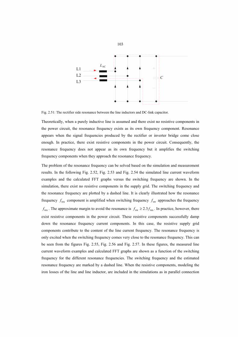
103
ACL
CL3L2L1
Fig. 2.51: The rectifier side resonance between the line inductors and DC-link capacitor.
Theoretically, when a purely inductive line is assumed and there exist no resistive components in
the power circuit, the resonance frequency exists as its own frequency component. Resonance
appears when the signal frequencies produced by the rectifier or inverter bridge come close
enough. In practice, there exist resistive components in the power circuit. Consequently, the
resonance frequency does not appear as its own frequency but it amplifies the switching
frequency components when they approach the resonance frequency.
The problem of the resonance frequency can be solved based on the simulation and measurement
results. In the following Fig. 2.52, Fig. 2.53 and Fig. 2.54 the simulated line current waveform
examples and the calculated FFT graphs versus the switching frequency are shown. In the
simulation, there exist no resistive components in the supply grid. The switching frequency and
the resonance frequency are plotted by a dashed line. It is clearly illustrated how the resonance
frequency resf component is amplified when switching frequency swf approaches the frequency
resf . The approximate margin to avoid the resonance is ressw 3.2 ff ≥ . In practice, however, there
exist resistive components in the power circuit. These resistive components successfully damp
down the resonance frequency current components. In this case, the resistive supply grid
components contribute to the content of the line current frequency. The resonance frequency is
only excited when the switching frequency comes very close to the resonance frequency. This can
be seen from the figures Fig. 2.55, Fig. 2.56 and Fig. 2.57. In these figures, the measured line
current waveform examples and calculated FFT graphs are shown as a function of the switching
frequency for the different resonance frequencies. The switching frequency and the estimated
resonance frequency are marked by a dashed line. When the resistive components, modeling the
iron losses of the line and line inductor, are included in the simulations as in parallel connection

104
with the line side inductor the resonance component is damped down, as suggested by the
measurement results.
00.02
0.040.06
0.08
6.2 7.7 9.1
11.112.5
14.316.7−20
−10
0
10
20
time [s]switching frequency [kHz]
line
curr
ent [
A]
00.5627
1
2x 10⁴
6.2 7.7
9.1 11.1
12.514.3
16.7
0
2
4
6
Switching frequency [kHz]frequency [Hz]
FFT
of
line
curr
ent [
A]
fres
fsw
2f
sw
Fig. 2.52: Waveform and FFT of the simulated line current as a parameter of the switching frequency. The DC-link capacitor is 2 µF and the line inductor 0.2 mH.

105
00.01
0.020.03
0.04
5
6.77.17.7
8.39.1
10−20
−10
0
10
20
time [s]switching frequency [kHz]
line
curr
ent [
A]
00.3979
0.61
1.5
2
x 104
5
6.77.17.7
8.39.1
10
0
5
10
Switching frequency [kHz]frequency [Hz]
FFT
of
line
curr
ent [
A]
2fsw
fsw
fres
Fig. 2.53: Waveform and FFT of the simulated line current as a parameter of the switching frequency. The DC-link capacitor is 2 µF and the line inductor 0.4 mH.

106
00.02
0.040.06
0.08
5 6.3 7.1 8.3 9.1 10 11.1
12.514.3−20
−10
0
10
20
time [s]switching frequency [kHz]
line
curr
ent [
A]
00.325 0.5
1
1.5
2
x 104
5 6.3 7.1 8.3 9.1 10
11.112.5
14.3
0
2
4
6
Switching frequency [kHz]frequency [Hz]
FFT
of
line
curr
ent [
A]
fres
fsw
2fsw
Fig. 2.54: Waveform and FFT of the simulated line current as a parameter of the switching frequency. The cc-link capacitor is 2 µF and the line inductor 0.6 mH.
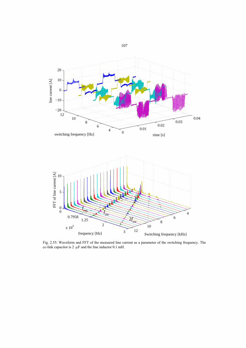
107
00.01
0.020.03
0.04
46
810
12−20
−10
0
10
20
time [s]switching frequency [Hz]
line
curr
ent [
A]
46
810
12
00.7958
1.252
3x 10
4
0
5
10
Switching frequency [kHz]frequency [Hz]
FFT
of
line
curr
ent [
A]
fres
fsw
2fsw
Fig. 2.55: Waveform and FFT of the measured line current as a parameter of the switching frequency. The cc-link capacitor is 2 µF and the line inductor 0.1 mH.

108
00.01
0.020.03
0.04
46
810
12−20
−10
0
10
20
time [s]switching frequency [Hz]
line
curr
ent [
A]
46
810
12
0
0.56271
1.52
x 104
0
5
10
Switching frequency [kHz]frequency [Hz]
FFT
of
line
curr
ent [
A]
fres
fsw
2fsw
Fig. 2.56: Waveform and FFT of the measured line current as a parameter of the switching frequency. The DC-link capacitor is 2 µF and the line inductor 0.2 mH.
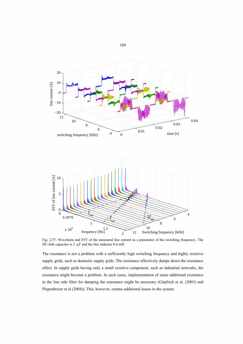
109
00.01
0.020.03
0.04
46
810
12−20
−10
0
10
20
time [s]switching frequency [kHz]
line
curr
ent [
A]
46
810
12
00.3979
11.5
2x 10
4
0
5
10
Switching frequency [kHz]frequency [Hz]
FFT
of
line
curr
ent [
A]
fres
fsw
2fsw
Fig. 2.57: Waveform and FFT of the measured line current as a parameter of the switching frequency. The DC-link capacitor is 2 µF and the line inductor 0.4 mH.
The resonance is not a problem with a sufficiently high switching frequency and highly resistive
supply grids, such as domestic supply grids. The resistance effectively damps down the resonance
effect. In supply grids having only a small resistive component, such as industrial networks, the
resonance might become a problem. In such cases, implementation of some additional resistance
in the line side filter for damping the resonance might be necessary (Göpfrich et al. (2003) and
Piepenbreier et al (2004)). This, however, creates additional losses in the system.

110
3 SINGLE-PHASE FED VOLTAGE SOURCE INVERTER
The high-capacitance single-phase fed VSI without power factor circuit creates a significant
amount of harmonic components in the line current. The simulated and measured behavior of the
traditional, single-phase fed VSI is shown in Fig. 3.1 and Fig. 3.2, respectively. The motor phase
currents are relatively sinusoidal and the DC-link voltage has only a moderate 100 Hz ripple.
However, the line current FFT shows a significant amount of harmonic components in the line
current waveform. A large DC-link capacitor causes high line current peaks during load of the
DC-link capacitor. Traditionally, power factor correction circuits are used to correct the quality of
the line current. To solve the problem of the line current quality and electrolytic capacitor, a small
MPPF capacitor is used. This leads to a heavily fluctuating DC-link voltage and torque. Many
industrial low performance applications, such as pumps and fans, are high inertia loads. Thus,
even heavily fluctuating torque can be tolerated.
0 0.01 0.02 0.03 0.04−0.5
0
0.5
Mot
or p
hase
cur
rent
s [p
u]
0 25 100 200 3000
0.1
0.2
0.3
0.4
0.5
FFT
of
mot
or p
hase
cur
rent
0 0.01 0.02 0.03 0.04−2
−1
0
1
2
Lin
e cu
rren
t and
uD
C [
pu]
time [s]0 500 1000 1500 2000
0
0.05
0.1
0.15
0.2
frequency [Hz]
FFT
of
line
curr
ent
time [s] frequency [Hz]
uDC
Fig. 3.1: Simulated behavior of the high-capacitance single-phase VSI motor phase currents, inverter line current and DC-link voltage with corresponding FFT figures. The motor phase currents waveforms are very sinusoidal. The line current waveform includes a high amount of harmonic components.
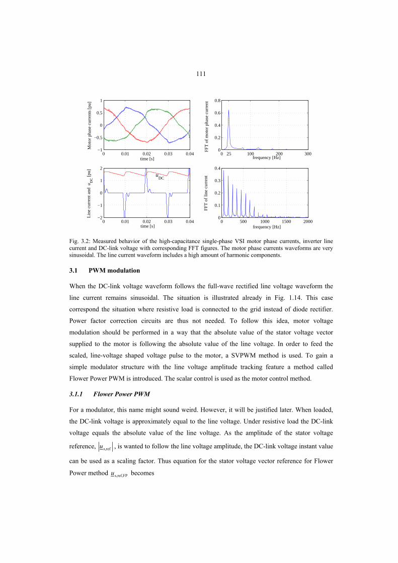
111
0 0.01 0.02 0.03 0.04−1
−0.5
0
0.5
1
Mot
or p
hase
cur
rent
s [p
u]
0 25 100 200 3000
0.2
0.4
0.6
0.8
FFT
of
mot
or p
hase
cur
rent
0 0.01 0.02 0.03 0.04−2
−1
0
1
2
Lin
e cu
rren
t and
uD
C [
pu]
0 500 1000 1500 20000
0.1
0.2
0.3
0.4
frequency [Hz]
FFT
of
line
curr
ent
time [s] frequency [Hz]
uDC
time [s]
Fig. 3.2: Measured behavior of the high-capacitance single-phase VSI motor phase currents, inverter line current and DC-link voltage with corresponding FFT figures. The motor phase currents waveforms are very sinusoidal. The line current waveform includes a high amount of harmonic components.
3.1 PWM modulation
When the DC-link voltage waveform follows the full-wave rectified line voltage waveform the
line current remains sinusoidal. The situation is illustrated already in Fig. 1.14. This case
correspond the situation where resistive load is connected to the grid instead of diode rectifier.
Power factor correction circuits are thus not needed. To follow this idea, motor voltage
modulation should be performed in a way that the absolute value of the stator voltage vector
supplied to the motor is following the absolute value of the line voltage. In order to feed the
scaled, line-voltage shaped voltage pulse to the motor, a SVPWM method is used. To gain a
simple modulator structure with the line voltage amplitude tracking feature a method called
Flower Power PWM is introduced. The scalar control is used as the motor control method.
3.1.1 Flower Power PWM
For a modulator, this name might sound weird. However, it will be justified later. When loaded,
the DC-link voltage is approximately equal to the line voltage. Under resistive load the DC-link
voltage equals the absolute value of the line voltage. As the amplitude of the stator voltage
reference, refs,u , is wanted to follow the line voltage amplitude, the DC-link voltage instant value
can be used as a scaling factor. Thus equation for the stator voltage vector reference for Flower
Power method FPref,s,u becomes

112
( ) ,32j
32
DCyref,s,xref,s,
DCrefs,FPref,s,
uuu
uuu
⋅+=
⋅= (3.1)
where the subscript FP stands for Flower Power.
Substituting this into the active time calculation equation (2.5), we notice from
( ) ( )
( ) ( ),
13πcos1
3πsin
3πcos
3πsin
32
32
13πcos1
3πsin
3πcos
3πsin
3
yref,s,
xref,s,s
DCyref,s,
xref,s,
DC
s
1
⎥⎦
⎤⎢⎣
⎡
⎥⎥⎥⎥
⎦
⎤
⎢⎢⎢⎢
⎣
⎡
⎟⎠⎞
⎜⎝⎛ −⎟
⎠⎞
⎜⎝⎛ −−
⎟⎠⎞
⎜⎝⎛−⎟
⎠⎞
⎜⎝⎛
=
⋅⎥⎦
⎤⎢⎣
⎡
⎥⎥⎥⎥
⎦
⎤
⎢⎢⎢⎢
⎣
⎡
⎟⎠⎞
⎜⎝⎛ −⎟
⎠⎞
⎜⎝⎛ −−
⎟⎠⎞
⎜⎝⎛−⎟
⎠⎞
⎜⎝⎛
=⎥⎦
⎤⎢⎣
⎡
+
uu
mm
mmT
uuu
mm
mm
uT
tt
m
m
(3.2)
that no information of the DC-link voltage is needed. This leads to a more simple structure of the
power circuit design. Also the modulator structure will be extremely simple.
This is the simplest way to make the motor rotate. To verify the idea and to show the basic
features of the studied method a simulation and measurements performed at an output frequency
of 25 Hz (0.5 pu) are given. The simulated and measured motor phase currents as well as the
frequency converter line current with corresponding FFT-figures are shown in Fig. 3.3. As it can
be seen, the motor phase currents are unorthodox but the line current waveform is very nice. Fig.
3.4 illustrates the simulated and measured xy-plot of the stator current vector trajectory is and the
DC-link voltage vector trajectory waveform describing the maximum available stator voltage
us,max. Since a 25 Hz (0.5 pu) frequency has been chosen the modulator using Flower Power
method carries out half of the available stator voltage us,ref,FP. The voltage vector trajectory plot in
the xy-coordination system justifies the term Flower Power for the modulator. The maximum
available voltage vector and also the stator voltage vector reference have the shape of a flower
petal.

113
a)
0 0.01 0.02 0.03 0.04−2
−1
0
1
2
Mot
or p
hase
cur
rent
s [p
u]
time [s]0 25 75 125 200 300
0
0.2
0.4
0.6
0.8
frequency [Hz]
FFT
of
mot
or p
hase
cur
rent
0 0.01 0.02 0.03 0.04−1
−0.5
0
0.5
1
Lin
e cu
rren
t [pu
]
time [s]0 500 1000 1500 2000
0
0.05
0.1
0.15
0.2
0.25
frequency [Hz]
FFT
of
line
curr
ent
b)
0 0.01 0.02 0.03 0.04−2
−1
0
1
2
Mot
or p
hase
cur
rent
s [p
u]
time [s]0 25 75 125 200 300
0
0.2
0.4
0.6
0.8
frequency [Hz]
FFT
of
mot
or p
hase
cur
rent
0 0.01 0.02 0.03 0.04−1
−0.5
0
0.5
1
Lin
e cu
rren
t [pu
]
time [s]0 500 1000 1500 2000
0
0.1
0.2
0.3
0.4
FFT
of
line
curr
ent
frequency [Hz]
Fig. 3.3: a) Simulated and b) measured motor phase currents and inverter line current with corresponding FFT figures. The motor phase currents waveforms are very unorthodox. The line current waveform is close to the sinusoidal and thus very desirable.

114
a)
−1.5 −1 −0.5 0 0.5 1 1.5−1.5
−1
−0.5
0
0.5
1
1.5
y [p
u]
x [pu]
is u
s,ref,FP u
s,max
b) −1.5 −1 −0.5 0 0.5 1 1.5
−1.5
−1
−0.5
0
0.5
1
1.5
y [p
u]
x [pu]
is u
s,max u
s,ref,FP
Fig. 3.4: a) Simulated and b) measured motor stator current vector trajectory is and the maximum stator voltage vector trajectory us,max and the modulated stator voltage vector trajectory us,ref,FP. The term Flower Power comes from the shape of the voltage vector trajectory.

115
3.1.2 SVPWM with estimated DC-link voltage
The Flower Power PWM is a very rough method. To improve the behavior of the motor
especially under low angular frequencies, the traditional scalar control with SVPWM modulator
and overmodulation I is used. The amplitude reference for the stator voltage vector is used when
sufficient DC-link voltage is available. When the DC-link voltage level is insufficient, the
amplitude is limited according to the principle of overmodulation I. To accomplish compensation
of the DC-link voltage variation, voltage feedforward from DC-link voltage is needed. Fig. 3.5
represents the simulated and measured xy-coordinate presentation of the voltage and current
vector trajectories. The idea, shown in both figures, is to use compensation of the DC-link voltage
according to the traditional scalar control and SVPWM with overmodulation I. This means that
the stator voltage vector reference, marked by a red curve, is used unchanged as long as the level
of the DC-link voltage remains sufficient. The level during which the DC-link voltage is
insufficient, the overmodulation I method limits the amplitude of the modulated stator voltage
vector, marked by a black curve, in order to reach the maximum available voltage vector. In both
figures, the maximum available voltage vector us,max trajectory, the stator voltage vector reference
us,ref trajectory, the modulated voltage vector us,mod trajectory and the stator current vector is
trajectory, marked by a green curve, are shown. The line current waveform is expected to differ
from sinusoidal. This is because the output power is not controlled according to the input power
equation (1.10). The motor phase currents and line current waveform measurement results with
corresponding FFT figures are shown in Fig. 3.6. From the figure it can be seen that the line
current waveform is not as close to the sinusoidal as under the Flower Power method shown in
Fig. 3.3. However, the waveform frequency content remains still very decent.

116
a) −1.5 −1 −0.5 0 0.5 1 1.5
−1.5
−1
−0.5
0
0.5
1
1.5
y [p
u]
x [pu]
us,mod
us,ref
us,max
is
b)
−1.5 −1 −0.5 0 0.5 1 1.5−1.5
−1
−0.5
0
0.5
1
1.5
y [p
u]
x [pu]
us,ref
us,max
us,mod
is
Fig. 3.5: a) Simulated and b) measured motor stator current vector trajectory (is, green curve) and maximum stator voltage vector trajectory (us,max, blue curve) and modulated stator voltage (us,mod, black curve) vector trajectory. The stator voltage vector reference (us,ref, red curve) is used unchanged during the period the DC-link voltage remains sufficient. When the DC-link voltage becomes insufficient the overmodulation I method limits the amplitude of the modulated stator voltage vector in order to reach the maximum available voltage vector.

117
0 0.01 0.02 0.03 0.04−1.5
−1
−0.5
0
0.5
1
1.5
Mot
or p
hase
cur
rent
s [p
u]
time [s]0 500 1000 1500 2000
0
0.2
0.4
0.6
0.8
frequency [Hz]
FFT
of
mot
or p
hase
cur
rent
0 0.01 0.02 0.03 0.04−1
−0.5
0
0.5
1
Lin
e cu
rren
t [pu
]
time [s]
0 500 1000 1500 20000
0.2
0.4
0.6
0.8
frequency [Hz]
FFT
of
line
curr
ent
Fig. 3.6: Measured motor phase currents and inverter line current with corresponding FFT figures under traditional DC-link voltage compensated scalar control with SVPWM and overmodulation I. The line current waveform is not as close to the sinusoidal as under the Flower Power method. However, the waveform frequency content remains still very decent.
When the aim is to achieve a very simple power electric hardware configuration, it should be tried
to eliminate from the system every unnecessary high precision measurement. In this case, the aim
is to replace the accurate DC-link voltage measurement with an estimation algorithm and a single
bit line voltage sign measurement. In the case of resistive load, the DC-link voltage equals the
absolute value of the line voltage. To estimate the DC-link voltage it is thus only necessary to
know the line voltage phase. Only a single-bit measurement of the line voltage sign is needed to
determine the phase. The peak value of the line voltage can be expected to be very close to its
normal value. The equation for uDC,estim is
( )gridgridL1estimDC, sinˆ φω += tuu , (3.3)
where L1u is the peak value for the line voltage, t is the time, gridω is the angular frequency of the
grid and the angle gridφ stands for the initial phase of the line voltage.
Due to the insufficient voltage, a negative torque is generated. Due to the negative torque the DC-
link voltage rises and therefore differs from the absolute value of the line the voltage waveform.

118
This causes an error in the DC-link voltage estimation. The negative torque during the low DC-
link voltage may be clearly seen from Fig. 3.7 (a) and (b). In the case of an ideal DC-link voltage
measurement, the SVPWM modulator forms duty cycles as shown in Fig. 3.7 (a). At 0.01 s, there
appears the effect of the energy returning from the motor during the negative torque. This
negative torque is shown in Fig. 3.7 (b).
a)
0 0.002 0.004 0.006 0.008 0.01 0.012 0.014 0.016 0.018 0.02 0
100
200
300
400
time [s]
u DC
[V]
0 0.002 0.004 0.006 0.008 0.01 0.012 0.014 0.016 0.018 0.02 0
0.2
0.4
0.6
0.8
1
time [s]
Dut
y cy
cles
[pu
]
uDC
measured
uDC
estimated
b)0 0.002 0.004 0.006 0.008 0.01 0.012 0.014 0.016 0.018 0.02
−0.2
−0.1
0
0.1
0.2
0.3
0.4
0.5
time [s]
t e [pu
]
Fig. 3.7: a) Simulated effect of the measured DC-link voltage in the formulation of the three-phase duty cycles and b) simulated electric torque under SVPWM with measured DC-link feedback. The energy returning from the motor during the negative torque causes the DC-link voltage to arise. When measured DC-link voltage feedback in SVPWM modulator is used the pulse width reference reacts on the voltage level. This can be seen at the 0.01 s time instant.
As a comparison to Fig. 3.7, the created three-phase duty cycles and the behavior of the torque
when using the estimated DC-link voltage are shown in Fig. 3.8 (a) and Fig. 3.8 (b) respectively.

119
When the DC-link voltage gets lower than what the reference voltage modulated to the motor, the
duty cycles are saturated to their maximum values. The estimation algorithm fails to estimate the
DC-link rising during the returning energy. It can be seen, when comparing Fig. 3.7 and Fig. 3.8,
that no substantial error occurs.
a)
0 0.002 0.004 0.006 0.008 0.01 0.012 0.014 0.016 0.018 0.02 0
100
200
300
400
time [s]
u DC
[V]
0 0.002 0.004 0.006 0.008 0.01 0.012 0.014 0.016 0.018 0.02 0
0.2
0.4
0.6
0.8
1
time [s]
Dut
y cy
cles
[pu
]
uDC
measured
uDC
estimated
b) 0 0.002 0.004 0.006 0.008 0.01 0.012 0.014 0.016 0.018 0.02
−0.2
−0.1
0
0.1
0.2
0.3
0.4
0.5
0.6
time [s]
t e [pu
]
Fig. 3.8: (a) Simulated effect of the estimated DC-link voltage in the formulation of the three-phase duty cycles and (b) simulated electric torque under SVPWM with estimated DC-link feedforward. The energy returning from the motor during the negative torque causes the DC-link voltage to arise. When estimated DC-link voltage feedforward in SVPWM modulator is used the pulse width references do not react on the voltage level. This can be seen at the 0.01 s time instant.
The measured DC-link voltage feedforward has been tested with the experimental device. Due to
the un-modeled features and other losses not included in the simulation model, the returning
energy during the negative torque does not cause as high a DC-link voltage rise as seen in the

120
simulations shown in Fig. 3.7 and Fig. 3.8. Basically this means that in the case of the
experimental device the estimated and measured DC-link voltage yield exactly the same three-
phase duty cycle waveforms. The measured DC-link voltage and SVPWM generated three-phase
duty cycles used are shown in Fig. 3.9.
0 0.0045 0.0085 0.0145 0.0185 0.020
100
200
300
400
time [s]
u DC
[V
]
0 0.0045 0.0085 0.0145 0.0185 0.020
0.2
0.4
0.6
0.8
1
time [s]
Dut
y cy
cles
[pu
]
Fig. 3.9: Measured DC-link voltage and the three-phase duty cycles used. Due to losses that are not included in the simulation model, the returning energy during the negative torque did not cause DC-link voltage to rise high. When measured DC-link voltage feedforward in SVPWM modulator is used the pulse width reference reacts to the voltage level. This can be seen at the 0.006 s time instant. In the case of the experimental device the estimated and measured DC-link voltage yielding exactly the same three-phase duty cycle waveforms.
3.2 Electromechanical resonance
In traditional electric drives the structures of the mechanical couplings should be chosen carefully
to avoid mechanical failures. In demanding motor drive applications like rolling mill drives, fast
torque transients have a serious drawback; they work as a stimulus for the mechanical vibrations.
To avoid this, extremely stiff constructions have been used in shafts and mechanical switches. In
many cases, lighter dimensioning would be advantageous, if mechanical vibrations could be
actively damped. Some papers present active suppression using controlled electrical drives (Jun-
Keun et al. 1995, Peter et al. 2001, Sarén et al. 2002b). Active suppression requires a dynamical
model of the whole drive and smooth controllable electric torque. In the case of constantly
fluctuating electric torque, the design of mechanical couplings is an even more crucial task. The
electric torque cannot be controlled to be smooth as assumed in the papers above.

121
A theoretical drawing of the mechanical system is illustrated in Fig. 3.10. A model of two-mass
system connected with the shaft having finite torsional stiffness is the simplest mechanical
resonant system. While it is the simplest mechanical resonant system model, it is also accurate
enough to produce a good model describing the wide range of different rotating systems
connected with the shaft.
mω lω
sJ l
1sJ m
1s
Ksh
mωmJ lJ
lω
shK
et sht
lt
etsht
sht
lt
Fig. 3.10: Mechanical two-mass model. Inertia J, torsional spring constant K, torque t and angular frequency ω. The subscripts m, e, l and sh denotes the motor, electric, load and shaft respectively.
The mechanical two-mass system can be presented as a state-space model
( ) ( ) ( ) ( )
( ) [ ] ( )tty
ttJ
tuJ
t
KKJ
J
t
x
xx
C
EB
A
43421
321321
444 3444 21
&
001
0
10
00
1
0
100
100
ll
m
shsh
l
m
=
⎥⎥⎥⎥
⎦
⎤
⎢⎢⎢⎢
⎣
⎡−
+
⎥⎥⎥⎥⎥
⎦
⎤
⎢⎢⎢⎢⎢
⎣
⎡
+
⎥⎥⎥⎥⎥⎥
⎦
⎤
⎢⎢⎢⎢⎢⎢
⎣
⎡
−
−
=
, (3.4)
where the input u(t)=te, output y(t)=ωm and the states [ ]Tshlm)( tt ωω=x .

122
The mechanic system produces resonance Ω1 and anti resonance Ω2 frequency peaks
l
sh2
lmsh1
π21
11π2
1
JK
JJK
=Ω
⎟⎟⎠
⎞⎜⎜⎝
⎛+=Ω
. (3.5)
A Bode-diagram, em tω , of the mechanical structure is shown in Fig. 3.11 and esh tt in Fig.
3.12. The mechanic system produces resonance and anti-resonance frequency peaks as mentioned
above. The simulated electric torque te with its calculated FFT for a single-phase fed VSI with
small DC-link capacitor is shown in Fig. 3.13. Due to the heavily fluctuating DC-link voltage, the
electric torque also fluctuates.
−100
−50
0
50
100
Mag
nitu
de (
dB)
100
101
102
103
104
−90
−45
0
45
90
frequency [Hz]
Phas
e (d
eg)
Ω1= 201 Hz
Ω2= 39 Hz
Fig. 3.11: Bode-diagram of em tω of the mechanical structure.

123
−50
0
50
100M
agni
tude
(dB
)
101
102
103
−360
−315
−270
−225
−180
frequency [Hz]
Phas
e (d
eg)
Ω1=201 Hz
Fig. 3.12: Bode-diagram of esh tt of the mechanical structure.
0 0.02 0.04 0.06 0.08 0.1 0.12 0.14 0.16 0.18 0.2−0.2
−0.1
0
0.1
0.2
0.3
time [s]
t e [pu
]
0 50 100 150 200 250 300 350 400 450 500 5500
0.05
0.1
0.15
0.2
frequency [Hz]
FFT
of
t e
Fig. 3.13: The electric torque and its FFT graph.
On comparing the frequency content of the electric torque shown in Fig. 3.13 and the Bode
diagrams of the mechanical structure (Fig. 3.11 and Fig. 3.12) it is clearly seen that the main
harmonic frequency of the electric torque, that is 100 Hz, is effectively damped in the electrical
angular frequency whereas the resonance frequency, 200 Hz, is the dominating mechanical

124
harmonic frequency. On the shaft the resonance frequency is the dominant component. In Fig.
3.14(a) a simulated mechanical shaft torque and its FFT are shown. In Fig. 3.14(b) the
corresponding measured shaft torque and its FFT are shown. The operating point is 0.8 pu electric
frequency. Even tough the nominal torque of the controlled motor is approximately 7.5 Nm the
shaft torque goes as high as the peak value of 40 Nm. The phenomenon of shaft torque is clear
and can be tracked to the mechanical resonance. It can be concluded that extra attention should be
given to the design of the mechanical couplings. Stiff couplings are needed to avoid resonance.
Particularly traditional, low stiffness, torque measurement shafts are not applicable in the case of
a single-phase supplied small DC-link capacitor VSI.
(a)
0 0.02 0.04 0.06 0.08 0.1−60
−40
−20
0
20
40
60
time [s]
Shaf
t tor
que
t sh [
Nm
]
0 100 200 300 400 5000
10
20
30
40
frequency [Hz]
FFT
of
shaf
t tor
que
t sh
(b)
time [s]
0 0.02 0.04 0.06 0.08 0.1−60
−40
−20
0
20
40
60
time [s]
Shaf
t tor
que
t sh [
Nm
]
0 100 200 300 400 5000
5
10
15
20
frequency [Hz]
FFT
of
shaf
t tor
que
t sh
Fig. 3.14: (a) Simulated and (b) measured shaft torque.
3.3 Performance measurements
How good is this small capacitor, single-phase fed VSI? One very good criterion is the
performance comparison with an unmodified commercial VACON NXL-device. Both modified
and unmodified inverters are used with scalar motor control and 10 kHz switching frequency. The
unmodified NXL is controlled with scalar control using the traditional SVPWM with DC-link
voltage feedforward. With the MPPF DC-link capacitor modified NXL, named here YSK, both
SVPWM methods, the Flower Power method and the traditional uDC-feedforward compensated
method, are tested. The basic diagram of the measurement setup is shown in Fig. 3.15. The input

125
power, which is the line voltage L1u and current L1i , is measured. Both of the VSI configurations
were used with equal output powers. The equal output power can be guaranteed by controlling the
mechanical speed mω of the fan. The loading variation is gained by varying the air inflow of the
fan.
commercial inverter
1.3kW, 2500rpm 3~ motor
uU, uV, uW
iU, iV, iW
mω
uL1, NiL1
Fig. 3.15: Measurement setup for constant output power using fan load.
Three different inflow values with different rotating speeds of the fan are tested. The following
figures Fig. 3.16, Fig. 3.17 and Fig. 3.18 show the input power of the inverter as a function of the
mechanical angular speed of the fan for these three different inflow values.
0
100
200
300
400
500
600
0.25 0.35 0.45 0.55 0.65 0.75 0.85 0.95
mechanical speed [pu]
Pin
[W]
NXLYSK Flower PowerYSK Udc compensated
Fig. 3.16: Measured input power of the compared devices with minimal fan load. The difference in input power is insignificant below 75% of the nominal speed.

126
0
100
200
300
400
500
600
700
0.25 0.3 0.35 0.4 0.45 0.5 0.55 0.6 0.65 0.7 0.75
mechanical speed [pu]
Pin
[W]
NXLYSK Flower PowerYSK Udc compensated
Fig. 3.17: Measured input power of the compared devices with medium fan load. The Flower Power can not take more than 50% of the nominal speed. The Udc compensated YSK remains competitive until 60% of the nominal speed.
0
100
200
300
400
500
600
700
800
0.25 0.3 0.35 0.4 0.45 0.5 0.55 0.6 0.65 0.7
mechanical speed [pu]
Pin
[W]
NXLYSK Flower PowerYSK Udc compensated
Fig. 3.18: Measured input power of the compared devices with full fan load. The Udc compensated YSK remains competitive until 60% of the nominal speed.

127
To define the different electrical behavior of the traditional NXL and DC-link capacitor modified
NXL device, named YSK, the following figures Fig. 3.19, Fig. 3.20 and Fig. 3.21 are shown. In
each of the figures the waveforms of the supply grid current, DC-link voltage and motor phase
currents are shown. The same mechanical output power could be ensured in observing the fan
rotating speed. The mechanical frequency is 0.5 pu in all of the cases.
0 0.02 0.04 0.06 0.08 0.1 0.12 0.14 0.16 0.18 0.2−20
−10
0
10
20
Supp
ly g
rid
curr
ent [
A]
time [s]
iL1,RMS
=2.9
0 0.02 0.04 0.06 0.08 0.1 0.12 0.14 0.16 0.18 0.20
100
200
300
Dc−
link
volta
ge [
V]
time [s]
0 0.02 0.04 0.06 0.08 0.1 0.12 0.14 0.16 0.18 0.2−4
−2
0
2
4
Mot
or p
hase
cur
rent
s [A
]
time [s]
iU,RMS
= 1.7
Fig. 3.19: Measured supply grid current, DC-link voltage and motor phase currents with full fan load for NXL-device.
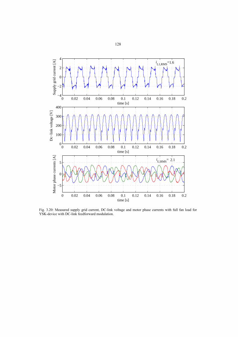
128
0 0.02 0.04 0.06 0.08 0.1 0.12 0.14 0.16 0.18 0.2−4
−2
0
2
4S
uppl
y gr
id c
urre
nt [
A]
time [s]
iL1,RMS
=1.6
0 0.02 0.04 0.06 0.08 0.1 0.12 0.14 0.16 0.18 0.20
100
200
300
400
Dc−
link
vol
tage
[V
]
time [s]
0 0.02 0.04 0.06 0.08 0.1 0.12 0.14 0.16 0.18 0.2
−5
0
5
Mot
or p
hase
cur
rent
s [A
]
time [s]
iU,RMS
= 2.1
Fig. 3.20: Measured supply grid current, DC-link voltage and motor phase currents with full fan load for YSK-device with DC-link feedforward modulation.

129
0 0.02 0.04 0.06 0.08 0.1 0.12 0.14 0.16 0.18 0.2−6
−4
−2
0
2
4
6Su
pply
gri
d cu
rren
t [A
]
time [s]
iL1,RMS
= 2.6
0 0.02 0.04 0.06 0.08 0.1 0.12 0.14 0.16 0.18 0.20
100
200
300
400
Dc−
link
volta
ge [
V]
time [s]
0 0.02 0.04 0.06 0.08 0.1 0.12 0.14 0.16 0.18 0.2−10
−5
0
5
10
Mot
or p
hase
cur
rent
s [A
]
time [s]
iU,RMS
= 3.6
Fig. 3.21: Measured supply grid current, DC-link voltage and motor phase currents with full fan load for YSK-device with Flower Power modulation.
Based on the additional losses due to the increased magnetic hysteresis losses and iron losses it is
suggested generally that the applications of the small capacitor single-phase fed VSI are among
those applications that have a low annual operating time but demand for line current with low
harmonic components. With Flower Power a very good grid behavior is gained. However the
efficiency gets poor when loading gets higher. This indicates that the Flower Power is
recommended for low dynamic applications which demand very good grid behavior, very low
annual operating time and which are not heavily loaded. Thus domestic appliances are very
tempting for this configuration. The single phase fed small DC-link capacitor VSI with traditional

130
DC-link voltage feedforward improves the loading capacity but the grid behavior is not as good as
with Flower Power. However this method is still more tempting than traditional high-capacitance
VSI when comparing the grid behavior. Manufacturing costs can be lowered by using the
estimated DC-link voltage. High-capacitance VSI has better efficiency. This makes the chose of
single phase fed small DC-link capacitor VSI with DC-link voltage feedforward and high-
capacitance VSI an optimization task between annual energy consumption and the repayment
period of the device. When smooth torque and when both annual operation time and the loading
are high, the high-capacitance VSI should be chosen.
Because of the lack of big energy storage in the DC-link, the average output voltage is smaller
compared with the traditional VSI with big DC-link capacitor. For this reason, a motor supplied
with a single phase fed small DC-link capacitor VSI needs to be redesigned and adapted to the
lower voltage level in order to gain enhanced performance. Since this kind of motor redesign has
not been carried out in this work it is not clear how much the performance can be enhanced with
proper motor design.

131
4 CONCLUSIONS
The need to improve the supply grid properties of the VSI is increasing. It is also sought for
solutions to lengthen the expected life-time of the frequency converter. The life time of the
frequency converter is expected to be increased by replacing its up to now “weakest link”, the
electrolytic DC-link capacitor, with a film capacitor. Film capacitors have a lower energy density
which leads to a smaller capacitance of the DC-link. This again leads to faster dynamics of the
DC-link voltage. The physical changes in the power electric hardware configuration remain small
when the electrolytic capacitor is replaced with a film capacitor of equal physical size having
traditionally only about 1 % of the electrolytic capacitance. It has, however, a significant impact
on the frequency converter dynamics and motor control algorithms. In order to compensate the
DC-link voltage fluctuation out from the VSI output voltage, faster controllers are needed.
The major part of all electric drives applications are low performance applications, such as pumps
and fans. In these applications the active rectifier bridge is hardly cost-effective. The supply grid
current harmonic content can thus not be controlled actively with the controlled rectifier bridge.
Traditionally, different types of passive filters are used. The physical size of the filters tends to be
large. By replacing the electrolytic capacitor with a film capacitor, the energy storage of the DC-
link decreases. Thus the instantaneous power supplied to the motor correlates with the power
drawn from the supply grid. This leads to a continuous DC-link current fed by the diode rectifier
bridge for which reason in the frequency converter with small DC-link capacitor the line current
harmonics are clearly decreased. Only a small AC-side filter is needed in the VSI with small DC-
link capacitor to filter the inverter bridge switching harmonics. When combining the reduced size
of the DC-link capacitor and the line side filter a more compact VSI is obtained.
4.1 Three-phase fed VSI
The frequency converter with a small DC-link capacitor shows very good line current properties
while the motor properties remain unchanged. No additional line side filter components are
needed. This simplifies the structure of the frequency converter. The modulator needs a
feedforward signal from the fluctuating DC-link voltage. The traditional SVPWM method
includes the DC-link voltage feedforward and uses it in the formulation of the switching
sequence.
When the capacitor is very small, every switching action of the power switches affects the DC-
link voltage. Thus, the constant DC-link assumption during the switching period leads to an error
in the produced voltage. The new modulating principle, named Differential Space Vector Pulse

132
Width Modulation (DSVPWM), being able to deal with the heavily fluctuating DC-link voltage,
produces the correct voltage vector with high accuracy.
The voltage source inverter with a small DC-link capacitor needs efficient overmodulation
methods. Since no energy storage exists in the DC-link, the DC-link voltage waveform follows
the rectifier bridge waveform. The region of overmodulation I starts at an earlier point because of
the voltage sags. The fundamental voltage fed to the motor can be increased smoothly from the
overmodulation I all the way up to the sixstep mode by using Constant Amplitude
overmodulation. The THD levels of the VSI with small DC-link capacitor are higher compared
with the VSI having the high-capacitance DC-link capacitor.
Due to the small DC-link capacitor, the DC-link voltage slew rate is much higher compared with
traditional high-capacitance converters. Traditionally, the measured DC-link voltage is used as a
feedback to point out the state of braking in scalar controlled VSI. With a small DC-link capacitor
the DC-link voltage can raise intolerably high even during a single switching period of the
modulator circuit. Therefore, when there is no speed encoder installed on the shaft, restraining the
scalar controlled motor drive from braking turns out to be a non-trivial task. To solve this
problem, a new overvoltage protection method, named DPFC, based on dynamic power factor
control has been introduced, studied and tested.
The DC-link capacitor combined with the line side inductance creates a resonance circuit.
Normally, the resonance frequency remains very low. Now, with the use of the small DC-link
capacitor and line side inductor, the resonance frequency significantly increases. The resonance
frequency can be close to or even higher than the switching frequency of the modulator. The
resonance phenomenon has been studied. A great number of simulation and measurement results
have been presented. The resonance is not a problem in highly resistive supply grids, such as
domestic supply grids. The resistance effectively damps down the resonance effect. In supply
grids having only a small resistive component, such as industrial networks, the resonance might
become a problem. In such cases, the implementation of additional resistance in the line side filter
might be required for damping the resonance.
4.2 Single-phase fed VSI
A single-phase fed VSI with a high-capacitance DC-link capacitor causes high line current peaks
during DC-link capacitor load. To solve the problem of the line current quality and electrolytic
capacitor, a relatively small MPPF capacitor is selected. If the DC-link capacitance is changed,
also the dynamic behavior of the single-phase fed frequency converter changes drastically. The
133
DC-link voltage and electric torque include heavy fluctuation. Because many industrial low
performance applications, such as pumps and fans, are high inertia loads, even heavily fluctuating
torque may thus be tolerated. In home applications the accuracy of the speed controller is not of
vital importance. A low line current harmonic content, however, is of crucial significance. By
using the Flower Power modulation method the sinusoidal line current waveform can be attained.
The performance of the single-phase fed VSI can be improved by using the DC-link voltage
feedforward. To reduce the expenses the DC-link voltage can be estimated from the sign of the
supply grid voltage. This means that the DC-link voltage feedforward can be achieved without
having to implement higher resolution voltage measurement in the DC-link.
During the design of the mechanical couplings of the single-phase fed small DC-link capacitor
VSI the constantly fluctuating electric torque has to be taken into account. The resonance
frequency of the two-mass system with finite torsional stiffness shaft can come close to the
fluctuating electric torque components. Simulation and measurement results illustrating the
problem have been presented.
Based on the additional losses due to the increased magnetic hysteresis losses and iron losses it is
suggested generally that the applications of the small capacitor single-phase fed VSI are among
those applications that have a low annual operating time but demand for line current with low
harmonic components. With Flower Power a very good grid behavior is gained. However the
efficiency gets poor when loading gets higher. This indicates that the Flower Power is
recommended for low dynamic applications which demand very good grid behavior, very low
annual operating time and which are not heavily loaded. Thus domestic appliances are very
tempting for this configuration. The single phase fed small DC-link capacitor VSI with traditional
DC-link voltage feedforward improves the loading capacity but the grid behavior is not as good as
with Flower Power. However this method is still more tempting than traditional high-capacitance
VSI when comparing the grid behavior. Manufacturing costs can be lowered by using the
estimated DC-link voltage. High-capacitance VSI has better efficiency. This makes the chose of
single phase fed small DC-link capacitor VSI with DC-link voltage feedforward and high-
capacitance VSI an optimization task between annual energy consumption and the repayment
period of the device. When smooth torque and when both annual operation time and the loading
are high, the traditional high-capacitance VSI should be chosen. These suggestions are confirmed
by the performance measurements with fan-load.

134
4.3 The future scope of the research
The future scope of the work will, unquestionably, concentrate on implementing more
sophisticated motor control algorithms, like current vector control, in the VSI with small DC-link
capacitor. When the small DC-link capacitor VSI is to be considered in high performance electric
drive applications the influence of the DC-link voltage fluctuation on the produced electric torque
needs to be investigated. Theoretically, no extra fluctuation in the electric torque is expected until
the overmodulation region starts. There is no known reason why the small DC-link capacitor
configuration couldn’t be used in high-performance drives.
The DC-link fluctuation causes extra harmonic distortion in the output voltage. As a result, the
efficiency decreases. As already mentioned, no drastic reduction of efficiency is expected and
thus the subject does not concern the author. However, in order to be able to find or even design
the optimal motor type for the small DC-link capacitor VSI, the additional distortion must to be
taken into consideration.
Although the DPFC with linear PID-controller proved to work satisfactory, more attention needs
to be paid to the controller. Finding a proper tuning method for the controller may be a subject for
future work. Future research should also focus on the possibility of implementing alternative
controller types into the DPFC method.
Traditionally, the impedance of the VSI filter has been the dominating part in the total line side
inductance. Now as the AC-filter impedance is reduced along the DC-link capacitor capacitance,
the supply grid impedance and AC-filter impedance values are now in the same decade. The
influence of the supply grid impedance on the line current resonance needs to be investigated at
different supply grid conditions.
Considering the single-phase supplied small DC-link capacitor VSI, attention may be paid to the
possibility of implementing other motor types for the modulators presented in this work. As the
reference publications suggest, the permanent magnet motor is the most interesting alternative
compared with the induction motor. Furthermore, it may be of interest to see what can be done in
designing a motor when the limitations in the supplied motor voltages of the single-phase
supplied small DC-link capacitor VSI are known beforehand.

135
References
Alaküla, M., Persson, J.E., 1994. Vector controlled AC/AC converters with a minimum of energy storage. Fifth International Conference on Power Electronics and Variable-Speed Drives, pp. 236-239.
Almeida, A., Fonseca, P., 1997. Characterisation of the electricity use in European Union and the saving potential in 2010, Energy efficiency improvements in electrical motors and drives. ISBN 3-540-63068-6.
ARC Advisory Group. 1998. AC Drive Worldwide Outlook, Market Analysis and Forecast Through 2002.
Blasko, V., 1997. Analysis of a hybrid PWM based on modified space-vector and triangle-comparison methods. IEEE Transactions on Industry Applications, Vol. 33, No. 3, pp. 756-764.
Bolognani, S., Zigliotto, M., 1996. Space vector Fourier analysis of SVM inverters in the overmodulation range. Proceedings of the 1996 International Conference on Power Electronics, Drives and Energy Systems for Industrial Growth, 1996. Vol. 1, pp. 319-324.
Bolognani, S., Zigliotto, M., 1997. Novel digital continuous control of SVM inverters in the overmodulation range. IEEE Transactions on Industry Applications, Vol. 33, No 2,pp. 525-530.
Bose, B. K., Kastha, D., 1991. Electrolytic capacitor elimination in power electronic system by high frequency active filter. Conference Record of the 1991 IEEE Industry Applications Society Annual Meeting, 1991. Vol. 1, pp.869-878.
Bose, B. K., 1997. Power Electronics and Variable Frequency Drives. IEEE Press, New York. ISBN 0-7803-1061-6.
Bramoulle, M., 1998. Electrolytic or film capacitors? IEEE Industry Applications Conference. Thirty-Third IAS Annual Meeting. Vol. 2, pp. 1138-1141.
Depenbrock, M., 1985. Direkte Selbstregelung (DSR) für hochdynamische Drehfeldantriebe mit Stromrichterspeisung, etzArchiv, Bd 7, Heft 7, pp. 211-218.
El-Husseini, M.H., Venet, P., Rojat, G., Al-Majid, A., Fathallah, M., 2001. Improving pulse handling capability of metalized polypropylene films capacitors. IEEE Industry Applications Conference, 2001. Thirty-Sixth IAS Annual Meeting. Conference Record. Vol. 4, pp. 2481-2486.
Gu, B.G., Nam, K., 2002. A DC link capacitor minimization method through direct capacitor current control. Conference Record of the Industry Applications Conference, 37th IAS Annual Meeting. Vol. 2, pp. 811-817.
Gu, B.G., Nam, K., 2005. Theoretical minimum DC-link capacitance in PWM converter-inverter systems. IEE proceedings on Electric Power Applications. Vol. 152, No 1, pp. 81-88.

136
Göpfrich, K., Rebbereh, C., Sack, L., 2003. Fundamental Frequency Front End Converter (F3E)- a DC-link drive converter without electrolytic capacitor. 24th International PCIM Conference 20.-22.5.2003 Nuremberg, Power Electronics, Intelligent Motion, Power Quality. Conference cd.
Haataja, J., Pyrhönen, J., 2002. Energy saving potential using high efficiency motor technology. Lappeenranta University of Technology, Department of Electrical Engineering. Research report 15. ISBN 951-764-673-9.
Haga, H., Takahashi, I., Ohishi, K., 2003. Direct Torque IPM Motor Control Method to Obtain Unity Power Factor Using a Single-Phase Diode Rectifier. IEEE International Electric Machines and Drives Conference, 2003. IEMDC'03.Vol. 2, 2003 , pp. 1078 - 1083
Hanitsch, R., 2002. Energy Efficient Electric Motors. RIO-02 World Climate & Energy Event, January 6-11, 2002.
Hava, A.M, 1998. Carrier Based PWM-VSI Drives in the Overmodulation Region. Dissertation, University of Wisconsin–Madison.
Holmes, D.G., 1996. The Significance of Zero Space Vector Placement for Carrier-Based PWM Schemes. IEEE Transactions on Industry Applications, Vol. 32, No. 5, pp.1122-1129.
Holtz, J., 1992. Pulsewidth Modulation – A Survey. IEEE Transactions on Industrial Electronics, Vol. 39. No. 5, pp. 410-420.
Holtz, J., 1993. On Continuous Control of PWM Inverters in the Overmodulation Range Including the Six-Step Mode. IEEE Transactions on Power Electronics, Vol. 8, No. 4, pp. 546-553.
Holtz, J., 1994. Pulsewidth Modulation for Electronic Power Conversion. Proceedings of the IEEE, Vol. 82, No. 8, pp.1194-1214.
Hur, N., Jung, J., Nam, K., 2001. A fast dynamic DC-link power-balancing scheme for a PWM converter-inverter system. IEEE Transactions on Industrial Electronics, Vol. 48, No. 4, pp. 794-803.
Imam, A., Habetler, T., Harley, R., Divan, D., 2005. Condition monitoring of electrolytic capacitor in power electronic circuits using adaptive filter modeling. IEEE 36th Annual Power Electronics Specialists Conference, 2005. Recife, Brazil. PESC05 conference cd. ISBN 0-7803-9034-2.
Jung, J., Lim, S., Nam, K., 1999. A feedback linearizing control scheme for a PWM converter-inverter having a very small DC-link capacitor. IEEE Transactions on Industry Applications, Vol. 35, No. 5, pp.1124-1131.
Jun-Keun, J., Seung-Ki, S., 1995. Kalman Filter and LQ Based Speed Controller for Torsional Vibration Suppression in a 2-Mass Motor Drive System. IEEE Transactions on Industrial Electronics, Vol. 42, No. 6, pp.564-571.

137
Kazmierkowski, M.P., Krishnan, R., Blaabjerg, F., Irwin, J.D., 2002. Control in Power Electronics: Selected Problems (Academic Press Series in Engineering). Academic Press; 1st edition (August 20, 2002), ISBN: 0124027725, 544 pages.
Kerkman, R.J.; Leggate, D.; Seibel, B.J.; Rowan, T.M., 1993, An Overmodulation Strategy for PWM Voltage Inverters. International Conference on Industrial Electronics, Control, and Instrumentation., Proceedings of the IECON '93., Vol. 2, pp. 1215-1221.
Kerkman, R.J.; Rowan, T.M.; Leggate, D.; Seibel, B.J., 1995, Control of PWM Voltage Inverters in the Pulse Dropping Region. IEEE Transactions on Power Electronics, Vol. 10, No. 5, pp. 559-565.
Kerkman, R.J., Leggate, D., Seibel, B.J.; Rowan, T.M., 1996, Operation of PWM Voltage Source-Inverters in the Overmodulation Region. IEEE Transactions on Industrial Electronics, Vol. 43, No. 1, pp. 132-141.
Kim, J.S., Sul, S.K., 1993. New control scheme for AC-DC-AC converter without DC link electrolytic capacitor. 24th Annual IEEE Power Electronics Specialists Conference, PESC 93 Record, pp. 300-306.
Kim, J.S., Sul, S.K., 1995. Resonant link bidirectional power converter. II. Application to bidirectional AC motor drive without electrolytic capacitor. IEEE Transactions on Power Electronics, Vol. 10, No. 4, 1995, pp.485-493.
Klumpner, C., Liserre, M., Blaabjerg, F., 2004. Improved control of an active-front-end adjustable speed drive with a small dc-link capacitor under real grid conditions. IEEE 35th Annual Power Electronics Specialists Conference, PESC 04. 2004. Vol 2, pp.1156-1162.
Kolar, J. W., Zach, F. C., 1994. A novel three-phase utility interface minimizing line current harmonics of high-power telecommunications rectifier modules. 16th International Telecommunication Energy Conference, IN-TELEC '94, Vancouver, Canada, pp. 367-374, October 1994. Conference proceedings.
Kovacs, K. P., Racz, I., 1959. Transiente Vorgänge in Wechselstrommaschinen, Band I. Budapest: Verlag der Ungarischen Akademie der Wissenschaften, 514p.
Kretschmar, K., Nee, H-P., 1998. An AC Converter with a Small DC Link Capacitor For A 15kW Permanent Magnet Synchronous Integral Motor. International Conference on Power Electronics and Variable Speed Drives, 21-23 September 1998, Conference Publication No. 456, IEE 1998.
Kretschmar, K., Nee, H-P., 2001. Analysis of the Efficiency and Suitability of Different Converter Topologies for PM Integral Motors. Australian Universities Power Engineering Conference (AUPEC 2001), Perth, Australia, September 2001. Conference proceeding.
Kretschmar, K., 2005. Main-Circuit Considerations of Power Converters for Integral Motors. Dissertation. Royal Institute of Technology, Department of Electrical Engineering, Electrical Machines and Power Electronics. Stockholm 2005. ISBN 91-7178-046-7.

138
Lamsahel, H., Mutschler, P., 2005. Control of a Permanent Magnet Synchronous Motor (PM) Fed by a Single-Phase Rectifier with Minimal DC-Link Capacitance. 26th International PCIM Conference. 7.-9.6.2005 Nuremberg, Power Electronics, Intelligent Motion, Power Quality. Conference cd.
Leonhard, W., 1996. Control of Electrical Drives. ISBN 3-540-59380, Springer-Verlag Berlin Heidelberg, Germany.
Michalczyk, P., Bramoulle, M., 2003. Ultimate properties of the polypropylene film for energy storage capacitors. IEEE Transactions on Magnetics. Vol. 39, Issue 1, pp. 362-365.
Military Handbook 217 F, “Reliability prediction of electronic equipment,” Revision F, Dec. 1991, Notice 1, 10 July 1992, Notice 2, Feb. 28, 1995.
Minari, Y., Shinohara, K., Ueda, R., 1993. PWM-rectifier/voltage-source inverter without DC link components for induction motor drive. Electric Power Applications, IEE Proceedings B. Vol. 140, No. 6, 1993, pp.363-368.
Peter, K., Scholing, I., Orlik, B., 2001. Robust state-feedback H ∞ control of a nonlinear two-mass system. Conference Record of the 2001 IEEE Industry Applications Conference, 2001. Thirty-Sixth IAS Annual Meeting ,Vol. 1, pp. 569 – 575
Phipps, J., K. 1997. A Transfer Function Approach to Harmonic Filter Design. IEEE Industry Applications Magazine, Vol. 3, No. 2, March-April 1997, pp.68 – 82.
Piepenbreier, B., Sack, L. 2004. Regenerative drive converter with line-frequency switched rectifier and without DC link components. IEEE 35th Annual Power Electronics Specialists Conference, 2004. PESC 04. Aachen Germany Vol. 5, 20-25 June 2004 pp. 3917 – 3923.
Pöllänen, R. 2003. Converter-Flux-Based Current Control of Voltage Source PWM Rectifiers – Analysis and Implementation. Dissertation. Lappeenranta University of Technology. ISBN 951-764-832-4.
Salo, M., 2002. Microcontroller Based Control of Current-Source PWM Converter Applications. Dissertation. Tampere University of Technology. ISBN 952-15-0942-2.
Sarén, H., Parviainen A., 2002a. Real Time Simulation and Measurement Environment of DC Converters for Educational Purposes. Proceedings SIMS 2002, University of Oulu, Oulu, Finland. ISBN 952-5183-18-1. 273 pages, pp 133-138.
Sarén, H., Pyrhönen, O. 2002b. Implementation of Active Vibration Suppression Using DTC Synchronous Motor Drive. Proceedings of Vibration and Acoustic Noise of Electric Machinery (VANEM) 2002, Technical University of Lodz, Poland. ISBN 83-909816-1-0. 134 pages, pp 83-87.
Sarén, H., Rauma, K., Pyrhönen, O. 2005. DTC Driven Single Phase Fed Voltage Source Inverter with Small DC-Link Capacitor. IEEE International Symposium on Industrial Electronics - ISIE 2005, 20.-23.6.2005, Dubrovnik, Croatia, 2005. ISBN 0-7803-8739-2.

139
Simulink, Dynamic System Simulation for MATLAB. November 2000, Revised for Simulink 4, Release 12.
Siyoung, K., Seung-Ki, S., Lipo, T.A., 1998. AC to AC power conversion based on matrix converter topology with unidirectional switches. Applied Power Electronics Conference and Exposition, 1998. APEC '98. Conference Proceedings 1998., Vol. 1, 15-19 February 1998 pp. 301 - 307.
Smith, S, W., 1999. The Scientist and Engineer's Guide to Digital Signal Processing. Second Edition. California Technical Publishing, USA. ISBN 0-9660176-7-6 hardcover, ISBN 0-9660176-4-1 paperback, ISBN 0-9660176-6-8 electronic.
Takahashi, I., Noguchi, T. 1986. A New Quick-Response and High-Efficiency Control Strategy of Induction Motor. IEEE Transactions on Industry Applications, Vol. 1A-22, No. 5, pp. 820-827.
Takahashi, I., Itoh, Y. 1990. Electrolytic capacitor-less PWM inverter. Proceedings IPEC-Tokyo, pp. 131-138.
Takahashi, I., Haga, H., 2001. Power factor improvement of single-phase diode rectifier by fast field-weakening of inverter driven IPM motor. 4th IEEE International Conference on Power Electronics and Drive Systems, 2001. Proceedings. Vol. 1, pp.241-246.
Takahashi, I., Haga, H., 2002. Inverter control method of IPM motor to improve power factor of diode rectifier. Proceedings of the Power Conversion Conference, 2002. PCC Osaka 2002. Vol. 1, pp.142-147.
Takahashi, I., Yamai, H. 2004. Inverter Control and its Device. Patent. EP1396927.
Tarkiainen, A., 2005. Power Quality Improving With Virtual Flux-based Voltage Source Line Converter. Dissertation. Lappeenranta University of Technology. ISBN 952-214-011-2.
Tiitinen, P., Pohjalainen, P., Lalu, J. 1995, The Next Generation Motor Control Method: Direct Torque Control (DTC), EPE Journal, Vol. 5, No 1, pp.14-18.
Van Der Broeck, H., Skudelny, H., Stanke, G. 1986. Analysis and realization of a pulse width modulator based on voltage space vectors. IEEE-IAS Conference. Records, pp 244-251, Denver, USA.
Wen-Song, C., Ying-Yu, T., 1998. Analysis and design on the reduction of DC-link electrolytic capacitor for AC/DC/AC converter applied to AC motor drives. 29th Annual IEEE Power Electronics Specialists Conference, PESC 98 Record, Vol. 1, pp. 275-279.

140
APPENDIX A, Simulation parameters for three-phase fed VSI
Nominal line-to-line RMS voltage Un = 400 V
Motor parameters:
Nominal power: 4 kW
Nominal current: 8.7 A
Nominal frequency: 50 Hz
Stator resistance: 0.03 pu
Stator leakage inductance: 0.1 pu
Stator magnetization inductance: 1.7 pu
Rotor leakage inductance: 0.1 pu
Rotor resistance: 0.025 pu
Frequency converter parameters:
Line side filter inductance: varied, for example 0.4 mH, 0.0047 pu.
Dc-link capacitor: varied, for example 2 µF, 0.0167 pu
Blanking time of IGBT switches: 2 µs
Minimum pulse of IGBT switches: 2 µs

141
APPENDIX B, Simulation parameters for single-phase fed VSI
Nominal line-to-zero RMS voltage Un = 230 V
Motor parameters:
Nominal power: 1.1 kW (VEM)
Nominal current: 4.55 A
Nominal frequency: 50 Hz
Stator resistance: 0.09 pu
Stator leakage inductance: 0.05 pu
Stator magnetization inductance: 1.77 pu
Rotor leakage inductance: 0.08 pu
Rotor resistance: 0.07 pu
Frequency converter parameters:
Line side filter inductance: varied, for example 0.4 mH, 0.0043 pu
Dc-link capacitor: varied, normally 3 µF, 0.0275 pu
Blanking time of IGBT switches: 2 µs
Minimum pulse of IGBT switches: 2 µs
Mechanical system parameters:
Motor inertia: 0.0035 kgm2 including motor inertia and half of the torque sensor inertia
Load inertia: 0.0146 kgm2 including load inertia and half of the torque sensor inertia
Shaft torsional spring constant: 6363 Nm/rad including the torque sensor spring constant

142
APPENDIX C, The parameters for three-phase fed test setup
The parameters of the motors are shown in Table1.
Table1: Controlled 4 kW motor and 5.5 kW load motor parameters for three-phase system.
Manufacturer and serial
number
Power
[kW] cosϕ
Nominal speed
[rpm]
Main voltage
[V]
Nominal
current [A]
Strömberg, SN 26383 B 4 0.83 1435 380 8.7
Strömberg SN 0566 MP 5.5 0.84 1440 380 11.7
Control board: dSPACE 1005
Control algorithms: Scalar control and SVPWM
Controller sample time: 25 µs
Switching frequency: varied, normally 10 kHz
Line side filter inductance: varied, normally 0.4 mH
Dc-link capacitor: varied, normally 2 µF

143
APPENDIX D, The parameters for single-phase fed test setup
The controlled motors are shown in Table 2. In verification measurements the 1.1 kW VEM
induction motor was used. In performance test carried out with fan load, the 1.3 kW Elektror
induction motor was used. The parameters for loading induction machine in verification
measurements are shown in Table 3.
Table 2: Controlled motor and load motor parameters for single-phase fed system.
Manufacturer Power
[kW] cosϕ
Nominal speed
[rpm]
Main voltage
[V]
Nominal
current [A]
VEM 1.1 0.8 1410 230 4.55
ELEKTROR 1.3 0.7 2480 220 - 300 4.8 - 4.2
Table 3: Load induction motor for single-phase fed system.
Manufacturer and serial
number
Power
[kW] cosϕ
Nominal speed
[rpm]
Main voltage
[V]
Nominal
current [A]
Strömberg, SN 24569 B 4 0.83 1435 380 8.7
Control board: dSPACE 1103
Control algorithms: Scalar control and SVPWM and SVPWM variations
Controller sample time for measurements: 25 µs
Switching frequency: varied, normally 10 kHz
Line side filter inductance: varied, normally 0.4 mH
Dc-link capacitor: varied, normally 3 µF
The fan performance measurement
Power analyzer: YOKOGAWA PZ4000 with low pass filter for all channels in 20 kHz.
YSK FlowerPower & YSK Udc compensation: 0.4 mH and 3 µF
NX Scalar control and SVPWM: 0.4 mH and 165 µF


ACTA UNIVERSITATIS LAPPEENRANTAENSIS 179. On the edge of fuzziness. Studies in honor of Jorma K. Mattila on his sixtieth birthday. Editors
Vesa A. Niskanen and Jari Kortelainen. 2004. 132 s. 180. VÄISÄNEN, PASI. Characterisation of clean and fouled polymeric membrane materials. 2004.
U.s. Diss. 181. IKÄVALKO, MINNA. Pas de deux of art and business: a study of commitment in art
sponsorship relationships. 2004. 277 s. Diss. 182. ENQVIST, YUKO. Comprehensive study of crystal growth from solution. 2004. U.s . Diss. 183. JÄPPINEN, PEKKA. ME – mobile electronic personality. 2004. U.s. Diss.
184. HALME, TAPANI. Novel techniques and applications in generalised beam theory. 2004. 101
s. Diss. 185. LOISA, ANTTI. Studies on integrating kinematic design method with mechanical systems
simulation techniques. 2004. 143 s., liitt. Diss. 186. 2nd Workshop on Applications of Wireless Communications. 2004. 74 s. 187. LI, XIAONING. Conflict-based method for conceptual process synthesis. 2004. U.s. Diss. 188. LAURILA, LASSE. Analysis of torque and speed ripple producing non-idealities of frequency
converters in electric drives. 2004. 124 s. Diss. 189. NIKULA, UOLEVI. Introducing basic systematic requirements engineering practices in small
organizations with an easy to adopt method. 2004. 207 s., liitt. Diss. 190. TANNINEN, JUKKA. Importance of charge in nanofiltration. 2004. U.s. Diss. 191. VIHTONEN, TIINA. Tuote- vai liiketoimintaosaamista? Pienten ja keskisuurten leipomoalan
yritysten strategiset valinnat, liikkeenjohdon käytännöt ja menestyminen. 2004. 238 s. Diss. 192. TURUNEN-SAARESTI, TEEMU. Computational and experimental analysis of flow field in the
diffusers of centrifugal compressors. 2004. 103 s. Diss. 193. SOLEYMANI, AZITA. Advanced topics in deformation and flow of dense gas-particle mixtures.
2004. U.s. Diss. 194. SALLINEN, PETRI. Modeling dynamic behavior in tilting pad gas journal bearings. 2004. 157
s. Diss. 195. HEILMANN, PIA. Careers of managers, comparison between ICT and paper business sectors.
2004. 262 s. Diss. 196. AHMED, MOHAMMAD. Sliding mode control for switched mode power supplies. 2004. U.s.
Diss. 197. HUPPUNEN, JUSSI. High-speed solid-rotor induction machine – electromagnetic calculation
and design. 2004. 168 s. Diss. 198. SALMINEN, PIA. Fractional slot permanent magnet synchronous motors for low speed
applications. 2004. 150 s. Diss. 199. VARIS, JARI. Partner selection in knowledge intensive firms. 2004. U.s. Diss. 200. PÖYHÖNEN, AINO. Modeling and measuring organizational renewal capability. 2004. U.s.
Diss.

201. RATAMÄKI, KATJA. Product platform development from the product lines´ perspective: case of switching platform. 2004. 218 s. Diss.
202. VIRTANEN, PERTTU. Database rights in safe European home: the path to more rigorous
protection of information. 2005. 425 s. Diss. 203. Säädöksiä, systematiikkaa vai ihmisoikeuksia? Oikeustieteen päivät 19. – 21.8.2003. Toim.
Marjut Heikkilä. 2004. 350 s. 204. PANTSAR, HENRIKKI. Models for diode laser transformation hardening of steels. 2005. 134
s., liitt. Diss. 205. LOHJALA, JUHA. Haja-asutusalueiden sähkönjakelujärjestelmien kehittäminen – erityisesti
1000 V jakelujännitteen käyttömahdollisuudet. 2005. 201 s., liitt. Diss. 206. TARKIAINEN, ANTTI. Power quality improving with virtual flux-based voltage source line
converter. 2005. U.s. Diss. 207. HEIKKINEN, KARI. Conceptualization of user-centric personalization management. 2005.
136 s. Diss. 208. PARVIAINEN, ASKO. Design of axial-flux permanent-magnet low-speed machines and
performance comparison between radial-flux and axial-flux machines. 2005. 153 s. Diss. 209. FORSMAN, HELENA. Business development efforts and performance improvements in
SMEs. Case study of business development projects implemented in SMEs. 2005. 209 s. Diss.
210. KOSONEN, LEENA. Vaarinpidosta virtuaaliaikaan. Sata vuotta suomalaista tilintarkastusta.
2005. 275 s. Diss. 211. 3rd Workshop on Applications of Wireless Communications. 2005. 62 s. 212. BERGMAN, JUKKA-PEKKA. Supporting knowledge creation and sharing in the early phases
of the strategic innovation process. 2005. 180 s. Diss. 213. LAAKSONEN, PETTERI. Managing strategic change: new business models applying wireless
technology as a source of competitive edge. 2005. 142 s. Diss. 214. OVASKA, PÄIVI. Studies on coordination of systems development process. 2005. U.s. Diss. 215. YANG, GUANGYU. Control and simulation of batch crystallization. 2005. U.s. Diss. 216. MUSTONEN–OLLILA, ERJA. Information system process innovation adoption, adaptation,
learning, and unlearning: a longitudinal case study. 2005. U.s. Diss. 217. SAINIO, LIISA-MAIJA. The effects of potentially disruptive technology on business model – a
case study of new technologies in ICT industry. 2005. 205 s. Diss. 218. SAINIO, TUOMO. Ion-exchange resins as stationary phase in reactive chromatography.
2005. 175 s. Diss. 219. CONN, STEFFEN. Software tools to support managers: development and application to new
product development and strategic alliance management. 2005. 168 s. Diss. 220. TYNJÄLÄ, TERO. Theoretical and numerical study of thermomagnetic convection in magnetic
fluids. 2005. U.s. Diss. 221. JANTUNEN, ARI. Dynamic capabilities and firm performance. 2005. 210 s. Diss. 222. KOLA-NYSTRÖM, SARI M. In search of corporate renewal: how to benefit from corporate
venturing? 2005. 190 s. Diss.