Embed Size (px)
Citation preview

ANALYSIS OF ANOMALOUS FILM GROWTH WHEN YTTRIUM OXIDE IS EXPOSED TO
VACUUM-ULTRAVIOLET LIGHT
Presenter: Devon R. Mortensen
Contributors: Thomas McConkie
David D. Allred
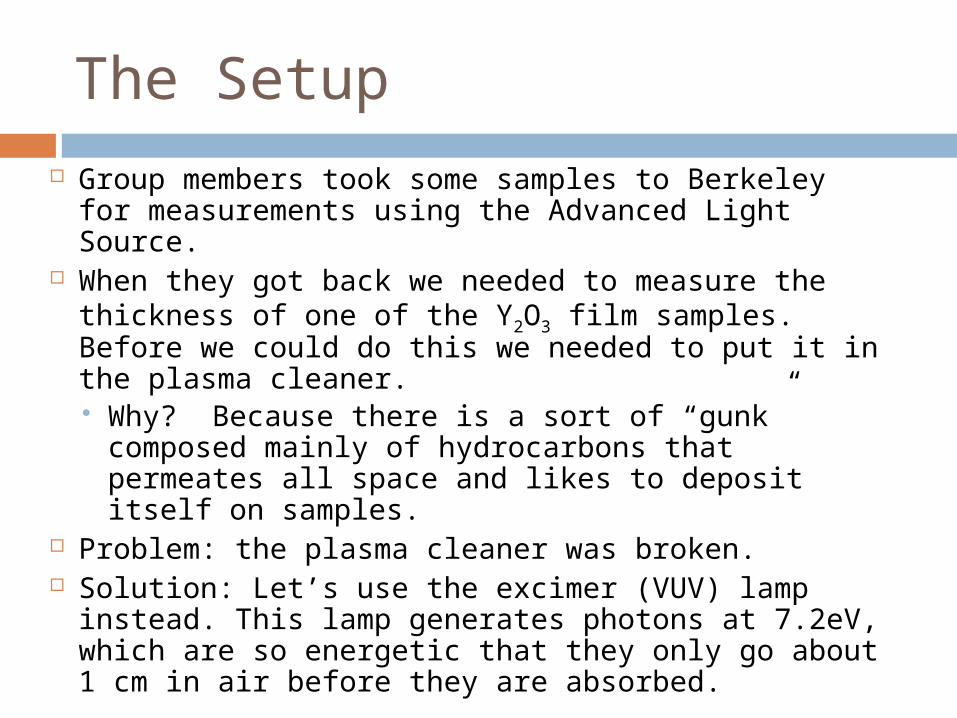
The Setup Group members took some samples to Berkeley for
measurements using the Advanced Light Source. When they got back we needed to measure the
thickness of one of the Y2O3 film samples. Before we could do this we needed to put it in the plasma cleaner. Why? Because there is a sort of “gunk”
composed mainly of hydrocarbons that permeates all space and likes to deposit itself on samples.
Problem: the plasma cleaner was broken. Solution: Let’s use the excimer (VUV) lamp instead.
This lamp generates photons at 7.2eV, which are so energetic that they only go about 1 cm in air before they are absorbed.

After approximately 5 minutes under the VUV lamp, the sample became visibly thicker.
Use ellipsometry measurements to determine if this is true. Before cleaning: 24.94 nm
0 si_jaw 1 mm1 sio2_jaw 2.000 nm2 ema y2o3/30% void 24.733 nm3 polycarb 0.000 nm4 srough 0.500 nm
Enter the Mystery
Generated and Experimental
Photon Energy (eV)1.0 2.0 3.0 4.0 5.0 6.0 7.0
Y in
de
gre
es D
in d
eg
ree
s
0
20
40
60
80
100
-200
-100
0
100
200Model Fit Exp Y -E 75°Model Fit Exp D-E 75°
Thick.2 =24.733±0.139 nm
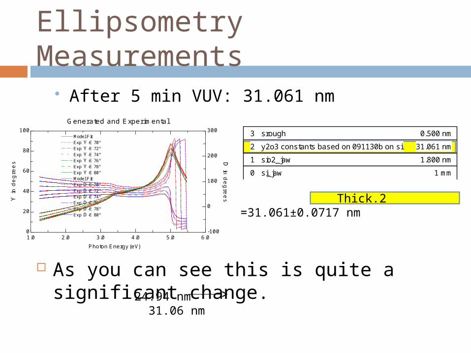
Ellipsometry Measurements
After 5 min VUV: 31.061 nm
As you can see this is quite a significant change.
Generated and Experimental
Photon Energy (eV)1.0 2.0 3.0 4.0 5.0 6.0
Y in
de
gre
es D
in d
eg
ree
s
0
20
40
60
80
100
-100
0
100
200
300Model Fit Exp Y -E 70°Exp Y -E 72°Exp Y -E 74°Exp Y -E 76°Exp Y -E 78°Exp Y -E 80°Model Fit Exp D-E 70°Exp D-E 72°Exp D-E 74°Exp D-E 76°Exp D-E 78°Exp D-E 80°
Thick.2 =31.061±0.0717 nm
24.94 nm 31.06 nm
0 si_jaw 1 mm1 sio2_jaw 1.800 nm2 y2o3 constants based on 091130b on si 31.061 nm3 srough 0.500 nm

Big question is: What’s going on here? First thought: the yttrium is not fully
oxidized.
Search for the Answer
If the yttrium were complete unoxidized expected film growth would be 3.34 nm
Actually film growth was 6.12 nm
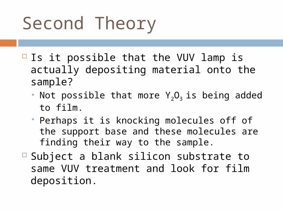
Second Theory
Is it possible that the VUV lamp is actually depositing material onto the sample? Not possible that more Y2O3 is being added to
film. Perhaps it is knocking molecules off of the
support base and these molecules are finding their way to the sample.
Subject a blank silicon substrate to same VUV treatment and look for film deposition.

Generated and Experimental
Photon Energy (eV)1.0 2.0 3.0 4.0 5.0 6.0 7.0
Y in
de
gre
es D
in d
eg
ree
s
0
10
20
30
40
50
0
30
60
90
120
150
180Model Fit Exp Y -E 75°Model Fit Exp D-E 75°
Before VUV:
After 5 min VUV:
0 si_jaw 1 mm1 sio2_jaw 2.221 nm2 y2o3 constants based on 091130b on si after 5 min vuv 0.000 nm3 srough 0.000 nm
0 si_jaw 1 mm1 sio2_jaw 2.074 nm2 y2o3 constants based on 091130b on si after 5 min vuv 0.000 nm3 srough 0.000 nm
MSE=5.786 Thick.1 =2.074±0.0081 nm
Generated and Experimental
Photon Energy (eV)1.0 2.0 3.0 4.0 5.0 6.0 7.0
Y in
deg
rees
D in degrees
0
10
20
30
40
50
0
30
60
90
120
150
180Model Fit Exp Y -E 75°Model Fit Exp D-E 75°
MSE=6.713 Thick.1 =2.221±0.00942 nm
Blank Silicon Wafer

0 si_jaw 1 mm1 sio2_jaw 1.797 nm2 y2o3 constants based on 091130b on si 0.000 nm3 srough 0.000 nm
After 10 min VUV:
After 25 min VUV:
Generated and Experimental
Photon Energy (eV)1.0 2.0 3.0 4.0 5.0 6.0 7.0
Y in
de
gre
es D
in d
eg
ree
s
0
10
20
30
40
50
0
30
60
90
120
150
180Model Fit Exp Y -E 75°Model Fit Exp D-E 75°
MSE=9.096 Thick.1 =1.797±0.012nm
Generated and Experimental
Photon Energy (eV)1.0 2.0 3.0 4.0 5.0 6.0 7.0
Y in
de
gre
es D
in d
eg
ree
s
0
10
20
30
40
50
0
30
60
90
120
150
180Model Fit Exp Y -E 75°Model Fit Exp D-E 75°
0 si_jaw 1 mm1 sio2_jaw 1.863 nm2 ema y2o3 constants based on 091130b on si after 10 min vuv/0% sio2_jaw0.000 nm3 srough 0.100 nm
MSE=8.125 Thick.1=1.863±0.0112nm
Blank Silicon Wafer

First Set of Conclusions
No apparent change in thickness of the silicon witness.
It doesn’t seem likely that the VUV lamp is depositing material onto our film.
Only other option is that what is already on the film is somehow being altered.
It is possible that the Y2O3 is catalyzing the oxidation of the silicon wafer underneath.
Let’s take a closer look at what is happening to the optical constants:

Optical Constants
At 2.4 eV (516 nm light) Y2O3 has an index of refraction of 1.938
Silicon dioxide has an index of 1.466 The formation of SiO2 should lower the
total index of the material. The data was fit using a Cauchy model,
allowing the parameters to vary to fit for optical constants.

Optical Constants
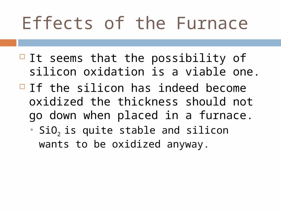
Effects of the Furnace
It seems that the possibility of silicon oxidation is a viable one.
If the silicon has indeed become oxidized the thickness should not go down when placed in a furnace. SiO2 is quite stable and silicon wants to be
oxidized anyway.
0 si_jaw 1 mm1 sio2_jaw 1.800 nm2 y2o3 constants based on 091130b on si 98.259 nm3 srough 0.500 nm
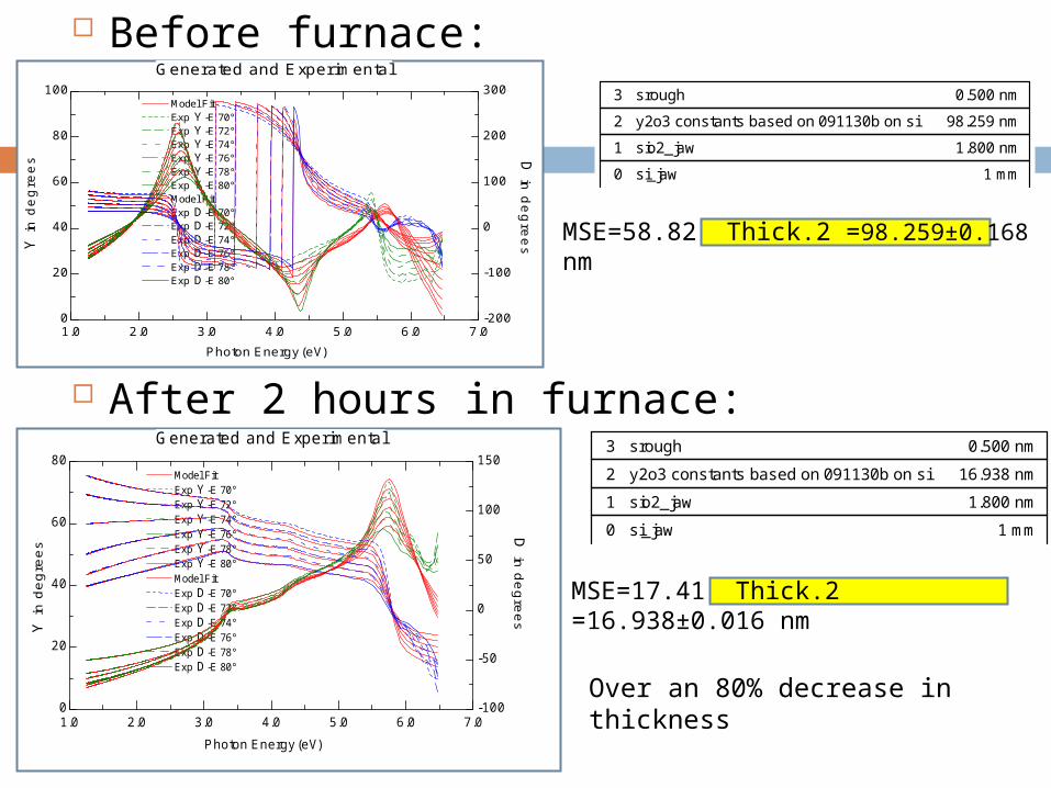
Before furnace:
After 2 hours in furnace:
Generated and Experimental
Photon Energy (eV)1.0 2.0 3.0 4.0 5.0 6.0 7.0
Y in
de
gre
es D
in d
eg
ree
s
0
20
40
60
80
100
-200
-100
0
100
200
300Model Fit Exp Y -E 70°Exp Y -E 72°Exp Y -E 74°Exp Y -E 76°Exp Y -E 78°Exp Y -E 80°Model Fit Exp D-E 70°Exp D-E 72°Exp D-E 74°Exp D-E 76°Exp D-E 78°Exp D-E 80°
Generated and Experimental
Photon Energy (eV)1.0 2.0 3.0 4.0 5.0 6.0 7.0
Y in
deg
rees
D in degrees
0
20
40
60
80
-100
-50
0
50
100
150Model Fit Exp Y -E 70°Exp Y -E 72°Exp Y -E 74°Exp Y -E 76°Exp Y -E 78°Exp Y -E 80°Model Fit Exp D-E 70°Exp D-E 72°Exp D-E 74°Exp D-E 76°Exp D-E 78°Exp D-E 80°
0 si_jaw 1 mm1 sio2_jaw 1.800 nm2 y2o3 constants based on 091130b on si 16.938 nm3 srough 0.500 nm
MSE=17.41 Thick.2 =16.938±0.016 nm
MSE=58.82 Thick.2 =98.259±0.168 nm
Over an 80% decrease in thickness

Maybe the sample is simply being puffed up.
Boiling water Ozonide
The Mystery Continues
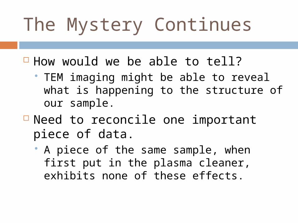
The Mystery Continues
How would we be able to tell? TEM imaging might be able to reveal what
is happening to the structure of our sample. Need to reconcile one important piece of
data. A piece of the same sample, when first put
in the plasma cleaner, exhibits none of these effects.