Embed Size (px)
Citation preview

HAL Id: hal-01019388https://hal.archives-ouvertes.fr/hal-01019388
Submitted on 8 Jul 2014
HAL is a multi-disciplinary open accessarchive for the deposit and dissemination of sci-entific research documents, whether they are pub-lished or not. The documents may come fromteaching and research institutions in France orabroad, or from public or private research centers.
L’archive ouverte pluridisciplinaire HAL, estdestinée au dépôt et à la diffusion de documentsscientifiques de niveau recherche, publiés ou non,émanant des établissements d’enseignement et derecherche français ou étrangers, des laboratoirespublics ou privés.
Analysis and Optimization of a Thyristor StructureUsing Backside Schottky Contacts Suited for the High
TemperatureGaëtan Toulon, Abdelhakim Bourennane, Karine Isoird
To cite this version:Gaëtan Toulon, Abdelhakim Bourennane, Karine Isoird. Analysis and Optimization of a ThyristorStructure Using Backside Schottky Contacts Suited for the High Temperature. IEEE Transactionson Electron Devices, Institute of Electrical and Electronics Engineers, 2013, 60 (11), p 3814-3820.�10.1109/TED.2013.2280554�. �hal-01019388�

> REPLACE THIS LINE WITH YOUR PAPER IDENTIFICATION NUMBER (DOUBLE-CLICK HERE TO EDIT) <
1
Abstract—In high current, high voltage, high temperature
(T>125°C) power applications, commercially available conventional silicon thyristors are not suited because they present high leakage current. In this context, this paper presents a high symmetrical (voltage) thyristor structure that presents a lower leakage current and higher breakover voltage as compared to the conventional thyristor at T>125°C. It is shown through 2D physical simulations that the replacement of the P emitter of a standard symmetrical thyristor by a judicious association of P diffusions and Schottky contacts at the anode side contributes to the reduction of the leakage current in the forward blocking state at high temperature. A fine-tune of the anode side configuration will improve the forward off-state behaviour with only a negligible on-state voltage drop degradation. Moreover, the comparison with the conventional anode short thyristor shows that the insertion of Schottky contacts leads to the same improvements in terms of off-state forward breakover voltage and leakage current and also presents a high reverse blocking voltage.
Index Terms— Pulsed power, High voltage thyristor, TCAD simulations, high temperature, Schottky contacts
I. INTRODUCTION
n high voltage and high current applications, such as HVDC transmission [1] or pulsed power application [2], a thyristor
is commonly used as a power switch because of its high power switching capabilities. The thyristor architecture is made of four layers of different doping forming an N-P-N and a P-N-P bipolar transistor. The maximum operating temperature of the commercially available symmetrical thyristors is generally limited to 125°C. Under high operating temperatures, the leakage current increases, amplified by the transistor gains, that leads to the parasitic latch-up of the thyristor.
Moreover, the temperature induced high leakage current can degrade the functioning of the whole power function in some cases. Indeed, in applications such as pulsed power circuits, as that shown in figure 1 [3], a capacitor is charged when the thyristor is maintained in off-state and it discharges through an R-L circuit when the thyristor is switched on. When the ambient temperature becomes high (T>125°C) the thyristor leakage current becomes high, deviating a part of the current
dedicated to the capacitor charging. It causes the degradation of the system operation, either by the reduction of the operating frequency of the system, or a system malfunctioning in the case of the thyristor parasitic latch-up.
Fig. 1: Example of a pulsed power circuit highlighting the thyristor role.
The generally approaches reported in literature for leakage current reduction focus on the current gain reduction of the internal bipolar transistors that compose the thyristor. Indeed, this can be achieved by different ways, such as: - Local electron or proton irradiation at the main junctions in order to reduce the carrier lifetimes [4] - N-type buffer layer between the N-base and P emitter - Anode short-circuits [5]
The two last techniques, which have already been demonstrated in high temperature applications [5], lead to a degradation of the reverse blocking capability, which means that additional components, such as a diode connected in series with the thyristor, must be added that leads to an increase in the number of components and cost.
Silicon carbide, thanks to its physical proprieties, could be considered for high temperature power applications. However, some technological issues still need to be solved, such as the reduction of basal plane dislocation density during thick epitaxial layers growth, which leads to a degradation of the carrier lifetime and then the increase of the on-state voltage drop, or the development of novel termination techniques for bi-directional blocking capability [6].
We propose a Si-thyristor structure based on the utilization of Schottky contacts associated to P diffusions at the backside of a symmetrical silicon thyristor [7] for symmetric blocking voltage as shown in figure 2. The Schottky contact on the thyristor anode side leads to a reduction of the emitter injection efficiency of the J2 junction, similar to conventional
Analysis and optimization of a thyristor structure using backside Schottky contacts
suited for the high temperature
G. Toulon1.2, A. Bourennane1.3, K. Isoird1
CNRS, LAAS, 7 avenue du colonel Roche, F-31400 Toulouse, France 2 Univ de Toulouse, LAAS, F-31400 Toulouse, France
3 Univ de Toulouse, UPS, LAAS, F-31400 Toulouse, France
I

> REPLACE THIS LINE WITH YOUR PAPER IDENTIFICATION NUMBER (DOUBLE-CLICK HERE TO EDIT) <
2
anode shorts, while preserving the reverse blocking capability of the device. The importance of the structure proposed in this paper is twofold: As compared to a symmetrical conventional thyristor of same size and physical parameters, it presents lower forward leakage current and higher breakover voltage mainly at ambient temperatures above 125°C.
In this paper, the impact of the insertion of Schottky contacts in the backside of a thyristor on its electrical characteristics is studied by means of TCAD simulations.
Fig. 2: Overview of the thyristor structure with Schottky contacts on the anode side.
II. LEAKAGE CURRENT REDUCTION METHODOLOGY
The leakage current in a thyristor in the forward blocking mode (VAK > 0) can be expressed by the following equation:
NPNPNP
CAK
II
αα −−=
10 (1)
Where IC0 is the leakage current of a PN junction in the blocking state and αPNP and αNPN the gain of the bipolar transistors composing the thyristor shown in figure 2.
The thyristor leakage current reduction can be achieved by minimizing IC0, αPNP and αNPN. The leakage current IC0 depends on the N-base doping concentration that sets the breakdown voltage of the device. Cathode shorts, usually used in commercial thyristor, reduce the N-P-N current gain during forward blocking mode through the reduction of RP-Base resistor (figure 2) that connects the base and emitter of this transistor. The configuration of these cathode shorts [8] has an influence on the N-P-N transistor current gain, the gate triggering current, and the device dV/dt capability. The P-N-P transistor gain can be lowered by the different methods presented in the introduction. We present in this paper a solution based on an association of Schottky contact and P diffusions as used in the JBS (Junction Barrier Schottky) diodes [9] at the thyristor
anode side, replacing the P emitter in the conventional thyristor for the reduction of the P-N-P transistor gain.
III. SIMULATION RESUTS
A. Studied structures
Three symmetrical thyristor structures are studied: a conventional one, a thyristor with Schottky contacts at the backside (figure 3 (a)) and a anode shorts thyristor (figure 3 (b)). This last structure is identical to the previous one, except that the backside electrode contacts an N+ diffusion instead of the N-base region. In order to achieve a symmetrical breakdown voltage, the N-base doping concentration is uniform and lightly doped in comparison with the P-type regions surrounding it. P-base and P-emitter junction depth are of 7µm, while the cathode N+ emitter and gate P+ diffusion depth are of 1µm. These values are in accordance with the technological process [10]. Different N+ emitter widths (Wcathode) and an anode width (Wa) of 100 µm are used. Cathode shorts are added for the reasons given previously.
Fig. 3: Schematic cross section of thyristor structures with (a) Schottky contact and (b) anode shorts.
All TCAD simulations have been performed with drift-diffusion model, as well as Shockley-Read-Hall (SRH) recombination model. Self-heating has not been considered in our simulations, especially in the off-state since the power dissipated in these cases is low. Schottky contacts have been simulated considering the barrier lowering effect [11]. A barrier height of 0.61V has been specified for the Schottky contact in the simulator, which represent a metal workfunction (ΦM) of 4.5V corresponding to Chromium (Cr) when deposited on N-type silicon.
B. Off-state
On figure 4 is represented the forward blocking voltage as a function of the N-base doping concentration and thickness for the three structures at a temperature of 27°C.

> REPLACE THIS LINE WITH YOUR PAPER IDENTIFICATION NUMBER (DOUBLE-CLICK HERE TO EDIT) <
3
1 2 3 4 51
2
3
4
5
67
For
war
d br
eako
ver
volta
ge (
1 ×× ××10
3 ) (V
)
N-base doping concentration (1××××1013) (cm-3)
WN = 600 µm
WN = 650 µm
WN = 700 µm
Closed symbols: conventional thyristorOpen symbols: Thyristor with Schottky contactsCross filled symbols: thyristor with anode shorts
Reachthrough
Avalanche breakdown
Fig. 4: Influence of the N-base parameters on the forward breakover voltage at 27°C.
For low values of the N-base doping concentration, the breakover voltage is limited by the reach-through of the base, leading to a reduction of the breakover voltage when lowering the doping concentration, while for high values, it is limited by the avalanche breakdown of the reverse biased J1 junction, which means that the increase of the doping concentration means a reduction of the breakover voltage. Consequently, for a given N-base layer thickness; there is an optimum doping concentration, which gives the highest breakover voltage. From the results on figure 4, at a fixed WN value, the insertion of Schottky contacts or anode short leads to an increase of the maximum breakover voltage. As a result, for an achievable breakover voltage, the N-base layer thickness can be lowered compared to the case of a conventional thyristor, leading to a reduction of the on-state voltage.
0 -1000 -2000 -3000 -4000 -5000 -6000
0,02
0,04
0,06
0,08
0,10
J AK (
A×× ××c
m-2)
VAK
(V)
WS = 0, 2, 4, 6 10, 20 µm
Fig. 5: Influence of the Schottky contact width on the leakage current, the value WS = 0 corresponds to a plane P-N junction.
The leakage current in a Schottky contact can be high
because of the barrier lowering effect under the presence of an electric field at the interface [11]. However, this degradation can be limited by the small spacing between two P diffusions, protecting the Schottky contact against excessive electric field values, as used in JBS diodes. This effect is illustrated on figure 5, where one can notice that the Schottky contact must be narrow in order to prevent the degradation of the reverse blocking characteristics of the thyristor.
On figure 6, the reverse characteristics of the thyristor with Schottky contacts and the conventional one are compared at different temperatures.
0 -1000 -2000 -3000 -4000 -5000 -600010-5
10-4
10-3
10-2
10-1
100
101
|JA
K (
A×× ××c
m-2)|
VAK
(V)
Conventional thyristor Thyristor with Schottky contact
27, 125, 150, 175 °C
Fig. 6: Influence of temperature on the reverse characteristics of the thyristor with Schottky contacts (Ws = 4 µm) and the conventional one.
The anode of the structure with Schottky contacts has been determined considering the previous simulations results. As a consequence, a Schottky contact width (Ws) of 4µm has been chosen and maintained constant in the following sections of this paper. A lower value would have given better results, but would have been very difficult to realize using the fabrication process used [10]. We can notice on figure 6 that both structures present the same breakdown voltage variation as function of temperature, but the presence of the Schottky contact leads to a soft transition near the avalanche breakdown because of the barrier lowering effect. However, a lower reverse leakage current could be expected with the use of a Schottky metal that is characterized by a higher barrier height, as detailed section 3.
0 50 100 150 2000
1
2
3
4
5
6
Closed symbols: conventional thyristorOpen symbols: thyristor with Schottky contactCross filled symbols: thyristor with anode shorts
For
war
d br
eako
ver
volta
ge (
1 ×× ××10
3 ) (V
)
Temperature (° C)
Wcathode
= 100 µm
Wcathode
= 200 µm
Fig. 7: Temperature effect on the forward breakdown for different N+ cathode widths.
Figure 7 shows the evolution of the forward breakover
voltage as a function of temperature for the three structures. For every structure, the reduction of the N+ cathode width

> REPLACE THIS LINE WITH YOUR PAPER IDENTIFICATION NUMBER (DOUBLE-CLICK HERE TO EDIT) <
4
(Wcathode) leads to an improvement of the forward breakover voltage at high temperatures. Indeed, when reducing Wcathode, the minimum gate current necessary to turn-on the device increases, because of the P-base resistance RP-base (figure 3) which is proportional to the N+ cathode width, meaning that the current flowing through this resistor required to forward bias the P-N junction between P-base and N+ must be high if the RP-base is small.
For a fixed value of Wcathode, the insertion of Schottky contacts or anode short leads to a reduction of injection efficiency of the J2 junction, because a part of the carriers are deviated through the Schottky contacts or the anode shorts. Consequently, this thyristor presents an improvement in its breakover voltage at a higher temperature as compared to a conventional thyristor. The variation of the breakover voltage with temperature of thyristors with Schottky contacts is identical to that of thyristors with anode shorts, meaning that the Schottky contact has the same effect as the anode short.
The forward blocking characteristics of the three structures is presented on figure 8. The lower leakage current in the thyristors with Schottky contacts and anode shorts as compared to the conventional thyristor case explain their improved off-state capability at high temperature.
0 1000 2000 3000 4000 5000 600010-5
10-4
10-3
10-2
10-1
100
101
125 °C
J AK (
A×× ×× c
m-2)
VAK
(V)
Conventional thyristor Thyristor with Schottky contact Thyristor with anode shorts
Wcathode
= 200 µm
27 °C
150 °C
175 °C
Fig. 8: Forward blocking characteristics of the three structures for different temperatures.
The reduced leakage current in the thyristor with Schottky contacts can be explained by comparing the transistors current gains αPNP and αNPN of both structures. In order to extract the different gains, several structures of identical sizes and parameters have been simulated and their leakage current evolution compared: the thyristor which are the subject of the study, a PN junction, a PNP and a NPN bipolar junction transistor (BJT). Figure 9 shows an example of leakage current simulated for the four structures. In this case, a conventional thyristor is compared with the three other structures.
0 1000 2000 3000 4000 500010-7
10-6
10-5
10-4
10-3
10-2
10-1
J AK (
A×× ××c
m-2)
VAK
(V)
Leakage current Thyristor NPN PN PNP
T = 27°C
0,0
0,2
0,4
0,6
0,8
1,0
αα αα
Gain αααα αααα
PNP
ααααNPN
ααααPNP
+ααααNPN
Fig. 9: Leakage current comparison of a conventional thyristor with three other structures of same size and transistors gain evolution with the applied voltage.
The curves of figure 9 show that the leakage current in the
PN junction and the NPN transistor are identical. It means that the current gain of the N-P-N transistor αNPN remains very weak. This low value comes from the presence of cathode shorts in the NPN transistor, as same as in the thyristor. The higher leakage current in the PNP transistor and the thyristor is due to the αPNP increase with the anode voltage. When the thyristor voltage reaches the breakover point, the P-N-P current gain value is equal to 1. The sum αNPN+αPNP is obtained from equation 1 by comparing the leakage current in the thyristor and in the PN junction. The sum of both transistor gains is almost equal to that of the P-N-P one as seen figure 9. Consequently, the conventional thyristor breakover voltage is mainly limited by the P-N-P current gain.
0 1000 2000 3000 4000 5000 60000,0
0,2
0,4
0,6
0,8
1,0
αα ααP
NP
VAK
(V)
Conventional thyristor Thyristor with Schottky contacts
Open symbols: T = 125°CClosed symbols: T = 27°C
Fig. 10: P-N-P transistor gain comparison for the thyristor with
Schottky contact and the conventional one at different temperatures. Figure 10 shows the evolution of the P-N-P transistor gain
as a function of the anode voltage for the thyristor with Schottky contact and the conventional thyristor. In the conventional thyristor, the αPNP increases more rapidly and reaches a value of 1 at a lower anode voltage. These results are in good agreement with the results from figure 8. The abrupt
> REPLACE THIS LINE WITH YOUR PAPER IDENTIFICATION NUMBER (DOUBLE-CLICK HERE TO EDIT) <
5
increase of αPNP in the thyristor with Schottky contacts at ambient temperature is mainly due to the avalanche because the injections of holes from the P-emitter are very low at this temperature.
C. On-state
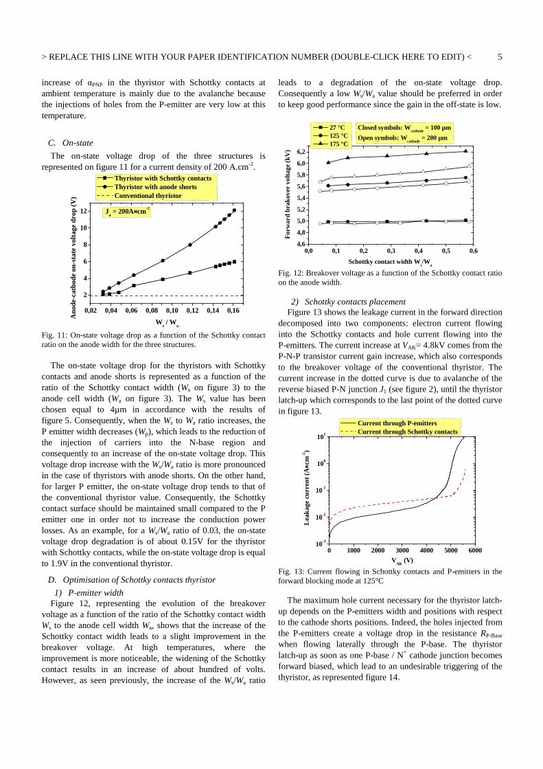
The on-state voltage drop of the three structures is represented on figure 11 for a current density of 200 A.cm-2.
0,02 0,04 0,06 0,08 0,10 0,12 0,14 0,16
2
4
6
8
10
12
Ano
de-c
atho
de o
n-st
ate
volta
ge d
rop
(V)
Ws / W
a
Thyristor with Schottky contacts Thyristor with anode shorts Conventional thyristor
Ja = 200A××××cm-2
Fig. 11: On-state voltage drop as a function of the Schottky contact ratio on the anode width for the three structures.
The on-state voltage drop for the thyristors with Schottky
contacts and anode shorts is represented as a function of the ratio of the Schottky contact width (Ws on figure 3) to the anode cell width (Wa on figure 3). The Ws value has been chosen equal to 4µm in accordance with the results of figure 5. Consequently, when the Ws to Wa ratio increases, the P emitter width decreases (Wp), which leads to the reduction of the injection of carriers into the N-base region and consequently to an increase of the on-state voltage drop. This voltage drop increase with the Ws/Wa ratio is more pronounced in the case of thyristors with anode shorts. On the other hand, for larger P emitter, the on-state voltage drop tends to that of the conventional thyristor value. Consequently, the Schottky contact surface should be maintained small compared to the P emitter one in order not to increase the conduction power losses. As an example, for a Ws/Wa ratio of 0.03, the on-state voltage drop degradation is of about 0.15V for the thyristor with Schottky contacts, while the on-state voltage drop is equal to 1.9V in the conventional thyristor.
D. Optimisation of Schottky contacts thyristor
1) P-emitter width Figure 12, representing the evolution of the breakover
voltage as a function of the ratio of the Schottky contact width Ws to the anode cell width Wa, shows that the increase of the Schottky contact width leads to a slight improvement in the breakover voltage. At high temperatures, where the improvement is more noticeable, the widening of the Schottky contact results in an increase of about hundred of volts. However, as seen previously, the increase of the Ws/Wa ratio
leads to a degradation of the on-state voltage drop. Consequently a low Ws/Wa value should be preferred in order to keep good performance since the gain in the off-state is low.
0,0 0,1 0,2 0,3 0,4 0,5 0,64,6
4,8
5,0
5,2
5,4
5,6
5,8
6,0
6,2
For
war
d br
akov
er v
olta
ge (
kV)
Schottky contact width Ws/W
a
27 °C 125 °C 175 °C
Closed symbols: Wcathode
= 100 µm
Open symbols: Wcathode
= 200 µm
Fig. 12: Breakover voltage as a function of the Schottky contact ratio on the anode width.
2) Schottky contacts placement Figure 13 shows the leakage current in the forward direction
decomposed into two components: electron current flowing into the Schottky contacts and hole current flowing into the P-emitters. The current increase at VAK= 4.8kV comes from the P-N-P transistor current gain increase, which also corresponds to the breakover voltage of the conventional thyristor. The current increase in the dotted curve is due to avalanche of the reverse biased P-N junction J1 (see figure 2), until the thyristor latch-up which corresponds to the last point of the dotted curve in figure 13.
0 1000 2000 3000 4000 5000 600010-3
10-2
10-1
100
101
Leak
age
curr
ent (
A ×× ××cm
-2)
VAK
(V)
Current through P-emitters Current through Schottky contacts
Fig. 13: Current flowing in Schottky contacts and P-emitters in the forward blocking mode at 125°C
The maximum hole current necessary for the thyristor latch-up depends on the P-emitters width and positions with respect to the cathode shorts positions. Indeed, the holes injected from the P-emitters create a voltage drop in the resistance RP-Base when flowing laterally through the P-base. The thyristor latch-up as soon as one P-base / N+ cathode junction becomes forward biased, which lead to an undesirable triggering of the thyristor, as represented figure 14.

> REPLACE THIS LINE WITH YOUR PAPER IDENTIFICATION NUMBER (DOUBLE-CLICK HERE TO EDIT) <
6
Fig. 14: Current distribution in the thyristor just after latch-up showing the non-uniform current distribution. The darker colors correspond to the higher current densities.
Since the maximum current density is at the middle of the
P-emitter width (see figure 15), it is necessary to place the cathode shorts in such a way that the hole current coming from the P emitter have the shortest path when flowing to the cathode shorts through the P-base. Consequently, every P-emitter should be aligned with a cathode short in order to achieve a higher voltage with a uniform latch-up of the thyristor.
Fig. 15: Hole current density distribution in the N-base close to
the anode electrode for VAK = 4.8kV Figure 16 shows the current distribution in the case of a
uniform latch-up of the device when considering the optimal configuration. The values considered in this case are Wcathode = WP = 100 µm. Moreover, this configuration would improve the dV/dt capability of the thyristor.
Fig. 16: Current density distribution in the thyristor just after the
latch-up in the optimal anode configuration. The darker colors correspond to the higher current densities.
3) Schottky contact barrier height
Different metals can be used for the realization of rectifying contact on silicon. The table 1 lists the barrier height of different metals on N-type silicon [12].
The ΦB values given in table 1 have been used in the
simulations for the forward and reverse blocking states. A lower value of ΦB of 0.5V has also been used in the simulations for comparison purposes. The results are shown on figure 17 and 18 respectively and compared to the characteristics of the conventional thyristor.
0 1000 2000 3000 4000 5000 600010-3
10-2
10-1
100
J AK (
A×× ×× c
m-2)
VAK
(V)
ΦΦΦΦB = 0,5 V ΦΦΦΦ
B = 0,67 V
ΦΦΦΦB = 0,61 V ΦΦΦΦ
B = 0,81 V
Conventional thyristor
T = 125°C
Fig. 17: Forward blocking characteristics of the thyristor with Schottky contact for different barrier heights
TABLE I SCHOTTKY BARRIER HEIGHT FOR METAL ON N-TYPE SILICON
Metal Cr W Pt Al
Work function ΦM (V) 4,5 4,6 5,3 4,25 Barrier height ΦB (V) 0,61 0,67 0,81 0,6

> REPLACE THIS LINE WITH YOUR PAPER IDENTIFICATION NUMBER (DOUBLE-CLICK HERE TO EDIT) <
7
The results in the forward blocking state show that the barrier height has only a minor influence on the leakage current, except for the value of 0.81V where the Schottky contact is no more efficient for the reduction of the P-N-P transistor gain and then of the leakage current.
0 -1000 -2000 -3000 -4000 -5000 -600010-3
10-2
10-1
100
101
J AK (
A×× ××c
m-2)
VAK
(V)
ΦΦΦΦB = 0,5 V ΦΦΦΦ
B = 0,67 V
ΦΦΦΦB = 0,61 V ΦΦΦΦ
B = 0,81 V
Conventional thyristor
T = 125°C
Fig. 18: Influence of the Schottky barrier height in the thyristor on
the reverse blocking characteristics On the contrary, the barrier height of the metal has an
influence on the reverse leakage current. The reduction of ΦB leads to a degradation of the reverse current leakage current in the thyristor. From these simulations, a Schottky barrier height of 0,67V presents the best trade-off between improvement in the forward blocking mode and degradation of the reverse leakage current.
IV. CONCLUSION
In this paper, different high voltage (5 kV) thyristor structures: a conventional symmetrical thyristor, an anode short thyristor and the proposed thyristor structure using Schottky contact at the anode side, have been compared in terms of on- and off-state electrical performance. The simulation results showed that the thyristor with Schottky contacts exhibits an improved forward breakover voltage at high temperature as compared to the conventional thyristor and presents a lower leakage current. These improvements in the blocking state electrical performance is achieved at the cost of only a slight degradation of the on-state voltage drop. Thanks to the use of Schottky contacts, the proposed thyristor structure exhibits the same performance gain of the anode short thyristor at high temperature, while preserving the reverse blocking capability, as same as in the conventional thyristor structure. These improvements are highly desirable for high voltage, high current pulsed power applications [13].
The structure optimisation method was detailed. We have shown by TCAD simulations that the arrangement of the Schottky contacts and P+ emitter diffusions have an impact on the forward and reverse electrical characteristics of the device. A fine tune of the anode configuration leads to an optimized trade-off between forward breakover voltage, on-state forward voltage drop and reverse blocking leakage current.
V. REFERENCES
[1] H. Peter Lips: Technology Trends for HVDC thyristor Valves, POWERCON, 1998, pp 451-455.
[2] E. Spahn, G. Buderer, J. Wey, V. Wegner, F. Jamet: The use of Thyristors as Main Switches in EML Applications, IEEE Trans. On Magnetics, Vol. 29 (1), 1993, pp 1060-1065.
[3] S. Scharnholz, V. Brommer, V. Zorngiebel, A. Welleman, E. Spahn: Performance study of a novel 13.5 kV multichip thyristor switch, PPC’09. 2009, pp 679-682.
[4] T. Nakagawa, K. Satoh, M. Yamamoto, K. Hirasawa, K. Ohta: 8kV/3.6kA Light Triggered Thyristor, ISPSD’95, 1995, pp 175-180.
[5] R. A. Kokosa, B. R. Tuft: A High-Voltage, High-Temperature Reverse Conducting Thyristor, IEEE Trans. Electron Devices, Vol 17 (9), 1970, pp 667-672.
[6] Q. Zhang et al.: SiC super GTO thyristor for technology development: Present status and future perspective, PPC’11, 2011, pp 1530-1535.
[7] P. Voss: Thyristor with reduced central zone thickness, US patent 5093705, 1992
[8] A. Munoz-Yague, P. Leturcq: Optimum Design of Thyristor Gate-Emitter Geometry, Trans. Electron Devices, Vol 23 (8) 1976, pp 917-924.
[9] B. J. Baliga: The Pinch Rectifier: A Low-Forward-Drop High-Speed Power Diode, IEEE Electron Device Letters, Vol. 5 (6), 1984, pp 194-196
[10] J-L Sanchez, P. Austin, M. Marmouget: Trends in design and technology for new power integrated devices based on functional integration, EPE’97, pp.1.302-1.307
[11] F. Lanois, F. Morancho: Caractéristiques électriques simulées et expérimentales de composants Schottky en tranchées, EPF 2004, pp 1-4 (in french).
[12] B. J. Baliga: Fundamentals of Power Semiconductor Devices, Springer, 2008.
[13] G. Toulon, A. Bourennane, K. Isoird : Analysis in commutation of a New High Voltage Thyristor Structure for High Temperature, MIXDES 2013, pp 426-430.